
SINGLE PALLADIUM NANOWIRE: SYNTHESIS VIA ...d-scholarship.pitt.edu/8320/1/07282008YushiHU.pdfSINGLE...
97
SINGLE PALLADIUM NANOWIRE: SYNTHESIS VIA ELECTROPHORESIS DEPOSITION AND HYDROGEN SENSING by Yushi Hu B.S. in Microelectronics Engineering, Fudan University, China, 2006 Submitted to the Graduate Faculty of the Swanson School of Engineering in partial fulfillment of the requirements for the degree of Master of Science University of Pittsburgh 2008
Transcript of SINGLE PALLADIUM NANOWIRE: SYNTHESIS VIA ...d-scholarship.pitt.edu/8320/1/07282008YushiHU.pdfSINGLE...

SINGLE PALLADIUM NANOWIRE: SYNTHESIS VIA ELECTROPHORESIS
DEPOSITION AND HYDROGEN SENSING
by
Yushi Hu
B.S. in Microelectronics Engineering, Fudan University, China, 2006
Submitted to the Graduate Faculty of
the Swanson School of Engineering in partial fulfillment
of the requirements for the degree of
Master of Science
University of Pittsburgh
2008
UNIVERSITY OF PITTSBURGH
SWANSON SCHOOL OF ENGINEERING
This thesis was presented
by
Yushi Hu
It was defended on
July 23, 2008
and approved by
Dr. Joel Falk, Professor, Department of Electrical and Computer Engineering
Dr. Kevin Chen, Associate Professor, Department of Electrical and Computer Engineering
Dr. Minhee Yun, Assistant Professor, Department of Electrical and Computer Engineering
Thesis Advisor: Dr. Minhee Yun, Department of Electrical and Computer Engineering
ii

Copyright © by Yushi Hu 2008
iii

SINGLE PALLADIUM NANOWIRE: SYNTHESIS VIA ELECTROPHORESIS DEPOSITION AND HYDROGEN SENSING
Yushi Hu, M.S.
University of Pittsburgh, 2008
Palladium (Pd) single nanowires with less than 100 nm thickness have been successfully
and repeatedly fabricated using electrophoresis deposition method. This work also demonstrates
the use of a single Pd nanowire as a hydrogen sensor with extremely high sensitivity. Growth
and sensing mechanisms are discussed in detail and an improved synthesis method is proposed
and proved.
Single Pd nanowires were electrodeposited within 100 nm wide Poly-Methyl-
Methacrylate (PMMA) nanochannels by using a probe station. The PMMA channels were
fabricated by Electron Beam Lithography (EBL) on a pre-patterned template fabricated via
photolithography and lift-off processes. Through this method, nanowires were grown with
widths ranging from 50 nm to 100 nm, and lengths from 3.5 µm to 6.5 µm. The nanowires,
successfully integrated into hydrogen sensor devices, were able to sense hydrogen concentrations
as low as 5 ppm (part per million) at room temperature. Three different nanowire structures were
found, and the growth control of nanowire structure was conducted. Different sensing
mechanisms were addressed in detail according to different nanowire structures.
A newly developed gate assisted growth method were also proposed and demonstrated in
this work. Thinner and more uniform nanowires were synthesized with this method, and the
growth time was greatly reduced. Experimental data were presented to approve the effects of
gate voltage on nanowire diameter and growth time.
iv

TABLE OF CONTENTS
PREFACE .................................................................................................................................. XII
1.0 INTRODUCTION ........................................................................................................ 1
1.1 MOTIVATION .................................................................................................... 1
1.2 THESIS ORGANIZATION ................................................................................ 4
2.0 BACKGROUND .......................................................................................................... 5
2.1 ONE DIMENSIONAL NANOSTRUCTURE AND NANOWIRE .................. 5
2.2 METALLIC NANOWIRE:PROPERTIES AND SYNTHESIS ...................... 8
2.2.1 Electrical Properties ..................................................................................... 9
2.2.2 Fabrication Techniques .............................................................................. 10
2.3 BASICS OF ELECTROPHORESIS AND ELECTRODEPOSITION ........ 14
2.3.1 Water and Ionic Solutions .......................................................................... 14
2.3.2 Mechanisms of Electrodeposition of Metals ............................................. 17
2.3.3 Nucleation and Growth Models of Electrodeposition.............................. 18
2.4 E-BEAM LITHOGRAPHY AND PMMA ..................................................... 20
2.4.1 PMMA:Properties and Applications as Resist ......................................... 20
2.4.2 E-Beam Lithography: Fundamentals and Processes ............................... 21
2.5 PALLADIUM AND HYDROGEN-PALLADIUM SYSTEM ....................... 22
2.5.1 General Properties of Palladium ............................................................... 22
2.5.2 Hydrogen Palladium System ...................................................................... 24
v

3.0 EXPERIMENT ........................................................................................................... 29
3.1 TEMPLATE PREPARATION AND NANOCHANNEL FORMATION .... 29
3.2 SINGLE NANOWIRE DEPOSITION VIA ELECTROPHORESIS DEPOSITION .................................................................................................... 32
3.2.1 Preparation of Electrolyte Solution ........................................................... 32
3.2.2 Nanowire growth ......................................................................................... 33
3.3 INTERGRATION OF SENSOR DEVICES ................................................... 36
3.4 GAS SENSING SYSTEM SET-UP .................................................................. 36
3.5 SIGNAL COLLECTION AND PROCESSING ............................................. 41
4.0 RESULTS AND DISCUSSION ................................................................................ 42
4.1 NANOWIRE GROWTH AND PROPERTIES .............................................. 42
4.2 NANOWIRE STRUCTURES AND GROWTH CONTROL ........................ 47
4.3 HYDROGEN SENSING: PERFORMANCE AND MECHANISMS ........... 52
4.4 GATE-ASSISTED NANOWIRE GROWTH .................................................. 62
5.0 CONCLUSION AND FUTURE WORK ................................................................. 71
5.1 CONCLUSION .................................................................................................. 71
5.2 LIST OF RESULTING PUBLICATIONS ...................................................... 73
5.3 FUTURE WORK ............................................................................................... 73
APPENDIX .................................................................................................................................. 76
BIBLIOGRAPHY ....................................................................................................................... 83
vi

LIST OF TABLES
Table 1. A recipe for a 100 nm feature size E-Beam Lithography Process .................................. 23
Table 2. Basic Properties of Palladium ......................................................................................... 25
Table 3. First few xnl values to make Bessel function zero .......................................................... 82
vii

LIST OF FIGURES
Figure 2.1.1. Illustration of (A) 3D, (B) 2D and (C) 1D structures ................................................ 5
Figure 2.3.1. Illustration of a common electrodeposition cell configuration ................................ 15
Figure 2.5.1. (A) A phase diagram showing the existence of α phase and β phase Palladium Hydrides. (B) A hysteresis shown for Hydrogen Palladium system at 120°C [44]. ......... 27
Figure 2.5.2. Relationships between H/Pd and R/R0. Hollow circle: 0°C; solid circle: 25°C; triangle: 50°C [46].. .......................................................................................................... 28
Figure 3.1.1. Fabrication process of template for 100 nm PMMA channels. A: 100 nm thick SiO2 growth; B: Photoresist spin-coating; C: Development of photoresist; D: E-beam evaporation of 5nm thick Ti layer as adhesion layer followed by 95nm thick gold layer as electrode. E: PMMA spin-coating; F: E-beam lithography and development of PMMA to pattern 100 nm wide nanochannels. .................................................................................. 30
Figure 3.1.2. (A) An AFM image of nanochannel together with electrodes on both sides. The size of the image is 8×8 µm2 and the channel length is 4.5 µm. (B) The 3-D view of the channel and electrodes. The height of the electrode is 100 nm and the depth of the channel is 100 nm. ............................................................................................................ 31
Figure 3.2.1. Probe station by The Micromanipulator Co. Inc. .................................................... 34
Figure 3.2.2. (A) Two probes provide a constant current through the channel during growth. (B) Voltage drop appears when nanowire growth is completed. ............................................ 35
Figure 3.3.1. (A) Illustration of a sensing device with wirebonded nanowire. (B) A real image of sensing fabricated sensor device. ...................................................................................... 37
Figure 3.4.1. Sensing system set-up.............................................................................................. 39
Figure 3.4.2. Reaction chamber (left) and gas mixing chamber (right) ........................................ 40
viii
Figure 4.1.1. An optical image with 150×10 times magnification of a grown nanowire. There are two pairs of electrodes (yellow) and two channels (tiny lines between the electrodes). The nanowire grown, which is in the bottom channel, can be barely seen. ............................. 43
Figure 4.1.2. A serial of SEM images for different nanowires with diameters of (A) less than 30 nm, (B) 63.58 nm, (C) 73.18 nm, (D) 96.58 nm, and (E) 103.5 nm. ................................ 44
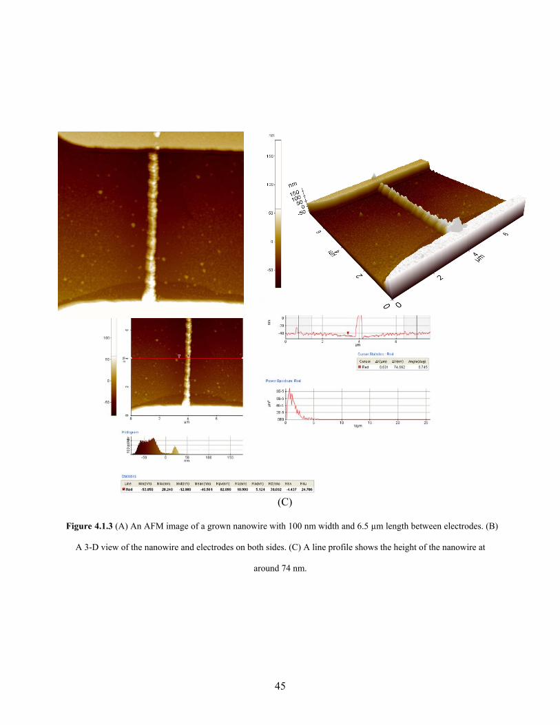
Figure 4.1.3. (A) An AFM image of a grown nanowire between electrodes with 100 nm width and 6.5 µm length. (B) A 3-D view of the nanowire and electrodes on both sides. (C) A line profile shows the height of the nanowire at around 74 nm. ....................................... 45
Figure 4.2.1. SEM images for three different nanowires structures: (A) and (B): Plain structure nanowires with 85 nm diameter; (C) and (D): Grain structure nanowires with diameter ranging from 100 nm to 150 nm; (E) and (F): Hairy structure nanowires with ~100 nm diameter............................................................................................................................. 48
Figure 4.2.2. SEM images for nanowires grown using three different currents: (A) 500nA growth current; (B) 100nA growth current. The upper left inset is a magnification of the left side, and the bottom right inset is a right side magnification; and (C) 50nA growth current. .. 50
Figure 4.2.3. Illustration of nanowire growth process. ................................................................. 51
Figure 4.3.1. A sensing result of ultra high sensitivity with a 1000 ppm – 100 ppm – 50 ppm – 20 ppm – 10 ppm – 5 ppm – 2 ppm – 1000 ppm – 100 ppm – 10 ppm – 5 ppm – 2 ppm sensing order. It is a positive signal. ................................................................................. 54
Figure 4.3.2. A sensing result of 5000 ppm hydrogen gas with negative signals. ........................ 54
Figure 4.3.3. A sensing result of 1% hydrogen with positive signal. The rise time is around 19 seconds. ............................................................................................................................. 55
Figure 4.3.4. SEM image of a plain structure nanowire with a negative signal. This nanowire has a diameter of 100 nm and length of 6.5µm. ...................................................................... 58
Figure 4.3.5. SEM image of a grain structure nanowire with a positive sensing signal. This nanowire has a diameter from around 150 nm to less than 30 nm; its sensitivity is 5 ppm............................................................................................................................................ 58
Figure 4.3.6. An illustration of a sensing mechanism of positive signals. The left side picture shows the change of neighboring grains and the size change on the neck. The right side picture shows the magnified view of the neck structure. .................................................. 59
Figure 4.3.7. (A) SEM image of a hairy structure nanowire. (B) 1% sensing signal of nanowire A. (C) SEM image of another hairy structure nanowire. (D) 1% sensing signal of nanowire C. ....................................................................................................................... 60
ix

Figure 4.4.1. Illustration of gate-assisted nanowire growth set-up. A, B, and C represent three different probes that connects to the semiconductor analyzer. Probes A and B connect to growth current, while probe C connects to a constant DC voltage as a gate. ................... 65
Figure 4.4.2. Band diagrams of the back gate structure (left) and illustrations of Pd2+ particles during growth (right) with (A) Vg = 0, (B) Vg > 0, and (C) Vg > 0. ................................. 66
Figure 4.4.3. Two nanowires with small and uniform diameters. (A) A grain structure nanowire with its smallest part less than 23 nm, and (B) A hairy structure nanowire with its smallest part less than 38 nm. ........................................................................................... 67
Figure 4.4.4. (A) The change of diameters from Vg= 0 to Vg= −10V under different conditions. (B) The change of growth time from Vg= 0 to Vg= −10 V under different growth conditions. ......................................................................................................................... 68
Figure A.1. Quantum conductance found in silver nanowires [26] .............................................. 79
Figure A.2. Illustration of an ideal nanowire structure ................................................................. 80
x
xi
PREFACE
I first thank my advisor, Dr. Minhee Yun. Without his relentless support, instruction,
patience, and advice, I could never have done this work. Even more importantly, his enthusiasm
in innovations, attitude towards research and optimism deeply impressed and encouraged me. I
am grateful to Dr. Yun on a professional and personal level.
I also thank Professor Joel Falk and Professor Kevin Chen for joining my committee and
giving me precious advice on my thesis. I further thank my fellow researchers, Dave Perello,
Innam Lee, Usman Mushtaq, and Dr. Hoil Park, for their continuous support.
Finally, I thank my parents for giving me the opportunity experience an intensive
education, and my girlfriend for her constant care and support.

1.0 INTRODUCTION
1.1 MOTIVATION The sensors industry has been considered one of the most important industries in the world. A
great deal of research has focused on ways to fabricate small, highly sensitive and energy
efficient sensors [1]. Among countless chemical sensors, hydrogen gas sensor emerges as a
special yet promising one. The hydrogen gas sensors are used widely in the gas storage and
fabrication industry for monitoring hydrogen concentration with security purposes. An increased
demand for faster and higher sensitive monitors emerges along with the development of
aerospace techniques and hydrogen fuel cell industry [2, 3]. Also, energy efficiency issues arise
with the development of green house and environment sustainability. Hydrogen sensors with a
smaller size, better performance, easier fabrication, and lower energy consumption have a
potentially large market [4].
Many researchers have focused on fabricating different hydrogen sensors, which can be
categorized into pyroelectric sensors, piezoelectric sensors, fiber optic sensors (FOS),
electrochemical sensors, and semiconductor (FET) sensors [5]. Within these sensors, a very high
sensitivity has been obtained by using the Pd-FET structure or FET structure coated with other
catalytic materials (Pt for example) and these structures are believed to be superior to other non-
FET sensors. However, they usually suffer from a high operation temperature and a more
1
complicated fabrication process [5]. New hydrogen sensors based on non-FET structures with
easy fabrication process and room temperature operation are needed.
The nanowire based hydrogen sensor is a very promising candidate in this regard.
Nanowires, either semi-conducting or metallic, have long attracted a great deal of attention
because of their unique properties [6]. Researchers have proposed nanosized structures or
devices with new and/or enhanced functions based on nanowires, such as field effect transistors
based on semiconductor nanowires [7], light emitting diode [8], biosensors [9], chemical sensors
[10], and thermocouples [11]. Defined as a one-dimensional (1D) structure, a nanowire often
refers to a wire with a diameter under 100nm and aspect ratio (length to width ratio) as large as
1000 [12]. Because of their small diameter, nanowires have a much larger surface to volume
ratio than thin films which are used in conventional FET or FOS structures. Higher surface could
facilitate higher sensitivity when sensing is based on surface interaction between catalytic
materials and sensing targets. This makes nanowire based nanosensors a powerful and general
class of ultrasensitive, electrical sensors for the direct detection of biological and chemical
species [13].
Hydrogen gas sensors based on metallic nanowire arrays [14] or bundles [15] have been
reported by multiple groups; these sensors excel in sensitivity or response time compared to
conventional non-FET sensors. They also show an advantage in easy fabrication since they are
based on pure Pd nanowires and, therefore, avoid the complicated process required by FET
sensors. However, they are still not comparable to FET sensors in sensitivity. A closer look
reveals that nanowire arrays or bundles are still based on the overall performance of a collection
of individual nanowires; this might undermine the advantages that an individual nanowire might
have. A single nanowire structure, which demonstrates a truly 1D structure, indicates higher
2
research value since the individual nanowire is being researched directly. Single nanowire
hydrogen gas sensors, taking full advantage of high surface to volume ratio, show great potential
in achieving higher sensitivity than arrays or bundles.
In spite of its advantage, the single nanowire device has always been difficult to fabricate
or align. Vapor-Liquid-Solid growth has been demonstrated as an effective fabrication method
for semiconductor nanowires, especially Si nanowire [7]. However, this process does require
high temperature or catalysts during the process. Chemical Vapor deposition (CVD), also
reported for nanowire growth, needs a complex fabrication process [16]. Besides, the alignment
of single nanowire should be addressed. As a controllable and feasible growth method,
electrochemical deposition could avoid these problems. By using a proper electrolyte solution,
Pd nanowire growth can be finished within a probe station at room temperature within minutes.
Meanwhile, the nanowire is self-aligned and connected to the electrodes, thereby avoiding the
alignment process [17].
Motivated by the above advantages, in this work Pd single nanowires are grown using
electrochemical deposition and hydrogen sensors are integrated based on them. Sensors with
high sensitivity, low power consumption, small size, and easy fabrication process are expected.
Additionally, the response of single nanowire to hydrogen and the idea that single nanowire has
advantage over traditional thin film or nanowire arrays are investigated. Finally, an entirely new
idea of electrodepositing nanowires with multiple electric fields is proposed and demonstrated.
3
1.2 THESIS ORGANIZATION Chapter 2 introduces the background information of this thesis. It presents the general ideas of
the one-dimensional structure and the advantages of nanowires. The properties of metallic
nanowires, especially conductance, and fabrication techniques are included. The key fabrication
processes, such as electrophoresis deposition and Electron-Beam Lithography, are fully
addressed. Palladium properties and hydrogen palladium interactions are also discussed.
Chapter 3 covers the experimental details of this work, including the complete template
fabrication process, electrophoresis deposition of the nanowire in probe station, sensor device
preparation and integration into the gas sensing system, and the set up of the gas sensing data
acquisition system.
Chapter 4 deals with the results and data from experiments with detailed analysis. The
growth of different nanowire structures and the control of nanowire structure are presented and
discussed. Hydrogen sensing signal and sensor performance are analyzed in detail, while the
relationship between the nanowire structures and the sensing mechanisms are presented. An
entirely new approach of gate voltage assisted nanowire growth is proposed and proved.
Chapter 5 draws the conclusions and summarizes the accomplishments of this work. The
potential of our research in biosensing area and possible future steps are included.
4

2.0 BACKGROUND
2.1 ONE DIMENSIONAL NANOSTRUCTURE AND NANOWIRE Dimensionality of substances, such as bulk materials, thin films, wires, and small particles, is
defined by the directions of high conductivity, or electron flow, in the material. In a three
dimensional or 3-D structure (Figure 2.1.1A), such as a gold brick, electrons flow freely in all
directions (x, y, z). However, in a two dimensional or 2-D structure (Figure 2.1.1B), such as
aluminum foil, electron flows are restricted in a plane (x-y plane). In a one dimensional or 1-D
structure (Figure 2.1.1C), such as a carbon nanotube, electrons can only flow in one direction
along the nanotube (y direction) but are very restricted in other directions (x, z). In a zero
dimensional structure, such as a gold nanoparticle, the electrons are limited inside the boundary
of a particle with zero direction to flow.
y
z 3-D 2-D 1-D
z z
y
x xA B C
x
Figure 2.1.1 Illustration of (A) 3D, (B) 2D, and (C) 1D structures.
Experimental studies of 1-D electronic systems could date back to the beginning of the
1970s when it first became possible to synthesize 1-D conductors [18]. Early research on 1-D
5
structures were initiated with the hope of realizing high temperature superconductors. While the
quest for high temperature superconductors has not been fulfilled in the past 40 years, the interest
in 1-D structures has never faded, especially when technology goes into nanometer range. 1-D
nanostructures, such as wires, belts, and tubes, are often referred to as those with lateral
dimensions that fall in the range of 1nm to 100nm. 1-D nanostructures have several
advantageous features:
The first feature is their small size. As predicted by Moore’s Law, the feature size of
Integrated Circuit devices is halved every 18 months. In the microelectronics area, a smaller size
means a higher device density, more functions, and better performance. With a lateral size
smaller than 100 nm, 1-D nanostructures might replace the conventional FET structures based on
bulk materials. FET structures based on semi-conducting nanowires, such as Si nanowires, have
been demonstrated by numerous reports [7, 19]. Moreover, 1-D nanostructures might also be
used as interconnect within CMOS structures. A field-programmable nanowire interconnect have
been proposed and facilitated in a nano CMOS architecture [20]. In addition to microelectronics,
1-D nanostructures could also be used in bio-molecular or bio-medical area where small size of
devices is a crucial issue.
Secondly, 1-D nanostructures are easily affected or confined by surface changes, such as
attachment of surface charges or change of chemical states, which makes them extremely
suitable for sensing purposes. For example, the effect of surface change in semi-conducting
oxides will become prominent when the effective diameter of the nanostructure becomes
comparable to the oxide’s Debye screening length [9]. In such nanostructures, a tiny change in
the chemical state of the surface due to the presence of chemical or biological agents can result
in the redistribution (depletion or accumulation) of electrons not only at near surface but also in
6

the entire volume of the nanostructure. This depletion (or accumulation), which will result in a
nontrivial signal that can be detected, thus enables the utilization of 1-D nanostructures as
sensors.
Thirdly, 1-D nanostructures have a large surface to volume ratio; this again proves that
they are very promising in sensors area. It can be easily substantiated that 1-D nanostructures
have the largest surface to volume ratio among 3-D, 2-D, and 1-D structures. In a block with
three dimensions of a, b, and c respectively, it can easily be calculated that the surface to volume
ratio in this case is:
: 2 / (2.1)
In 3-D structures, a, b, and c are big and comparable to each other. Therefore equation (2.1) can
be simplified as:
3 2 1/ 1/ 1/ , ~ ~ (2.2)
In 2-D structures, a and b are big, but c is much smaller than a or b. Equation (2.1) then becomes:
2 2 1/ , ~ (2.3)
In 1-D structures, a is big, and b and c are u aller than a. Equation (2.1) becomes: m ch sm
1 ~ (2.4) 1 2 1/ / ,
It is clear that 1 2 3 . It is also clear from equation (2.4)
that the surface to volume ratio is going to increase as the lateral dimensions decrease. With the
largest surface to volume ratio among the three, 1-D nanostructures provide most surface
reactive sites within certain volume, thus providing the best sensitivity.
Lastly, 1-D nanostructures exhibit many unique electrical and optical properties which,
by providing fundamental understanding of physics in nanometer range, deserve an in-depth
investigation. Electron transport in 1-D nanostructures is always an interesting issue. When the
7
diameter of 1-D nanostructures approaches the mean free path of electrons, the quantum effect of
electron transportation is expected to take place. Researchers have conducted many studies in
order to determine the quantum conductance of metallic nanowires; these studies have yielded
interesting results [21]. Photoluminescence in 1-D nanostructures, such as Carbon Nanotubes
(CNTs) and silicon or other semiconducting nanowires (NWs), and its potential use as Light
Emitting Diodes (LEDs), is another issue under intense investigation. In addition, free-standing
semiconducting nanowires can also act as stand-alone optical waveguides, cavities, and gain
medium to support laser emission [22].
2.2 METALLIC NANOWIRE: PROPERTIES AND SYNTHESIS
Semiconducting nanowires, such as silicon nanowires, germanium nanowires, and GaAs
nanowires, have been thoroughly investigated thoroughly because of their better compatibility
with today’s microelectronics industry and their potential in replacing conventional FET
structures [7]. In addition, the properties of semiconducting nanowires or organic nanowires,
such as easier surface modification and tunable sensitivity presented in FET structures, make
them perfect candidates in the area of bio-sensors. Metallic nanowires, on the other hand, are
explored primarily for their fundamental physical properties, such as quantum conductance [23],
phase change and superconductivity [24]. Very few studies focus on their usage as nano devices
such as sensors because of the lack of an easy and efficient fabrication method. The following
subsection discusses some basic physical properties of nanowire conductance; this second part
also includes fabrication techniques for metallic nanowires.
8

2.2.1 Electrical Properties Metallic nanowire conductance has been a research focus for many years. Researchers have tried
hard to discover how the conductance changes along with the diameter of nanowires. It is
generally accepted that when the diameter of the nanowires approaches the mean free path of the
electrons inside the nanowires, the electron transport should conform to the size dependent
quantum effects [21]. Rather than the general expression of conductance:
/ , (2.5)
in which G represents the conductance, σ represents conductivity, A represents the area and L
represents the length of the sample. Landauer’s Formula offers a more accurate expression for
conductance [21]:
2 / , (2.6)
where e represents the electron charge, h represents the Plank constant, and T represents the
transmission function that expresses the probability of transmitting an electron from one end of
the conductor to the other end.
According to Eq. 2.6, by assuming the nanowire satisfies ballistic scattering for electrons we can
draw a conclusion that the conductance of nanowire varies with its diameter. The conductance
becomes smaller when the diameter is decreased and quantum conductance effect could happen
when the diameter approaches the size of atoms. A complete explanation is included in the
Appendix part.
9
2.2.2 Fabrication Techniques How to grow nanowire arrays or bundles or single nanowires is always a critical part in nanowire
related research. As mentioned above, semi-conducting and metallic nanowires have found their
future applications in a wide range of areas, such as microelectronic circuits, chemical and bio
sensors and superconductivity, etc. Scientists, engineers and other industry people now seek an
efficient, economic, consistent, and easy to control technique of nanowire fabrication. While
different research groups have proposed multiple methods for semi-conducting nanowire growth,
including Laser Ablation [28], Chemical Vapor Deposition [29], and Self-Assembly [30], only a
limited number of fabrication techniques are introduced for metallic nanowire. The synthesis
techniques of metallic nanowire mainly fall into two categories: physical route and
electrochemical deposition route.
2.2.2.1 Physical Route. Metallic nanowires have been successfully fabricated using physical
methods without any chemical reactions, such as applying an electron beam bombardment on
thin films and thinning the wire via electron beams. In order to study the quantization of
nanowire conductance and the mechanical properties, thin wires down to a few angstroms could
be made by stretching. Other physical processes, such as physical evaporation, have also been
applied for conducting nanowire synthesis.
Forming a nanosized metallic nanowire using electron beam irradiation on thin films was
explained in detail by Takayanagi [31, 32]. A gold (011) film of thickness 3–5 nm was used as
the raw material. Electron beam irradiation was used to clean the film before putting the film
under an intense electron beam (200 kV, 500 A/cm2). A weaker electron beam (10–50 A/cm2)
was used for further thinning; new structures with diameters 0.6–1.5 nm and length 3–15 nm
10
were formed. High resolution tunneling electron microscopy revealed that the wires had a few
atom rows [32].
Stretching a wire into an even smaller size by applying a tensile stress on both ends has
been a commonly used method in fabricating nanowires with diameters of a few nanometers or
even a few angstroms [33]. This method, based on the elasticity or mechanical properties of the
material itself, can make a nanowire as thin as a few angstroms, depending on the specific
material. However, the short length (less than a few nanometers) of this kind of nanowire limits
the utilization of these nanowires in devices.
Physical evaporation is another technique for fabricating metallic or other conducting
nanowires. Yanfa Yan et al. [34] reported metallic zinc nanowires synthesized by physical
evaporation. They carried out the synthesis process in a quartz tube, using NH3 as a carrier gas
kept at a flow rate of 46 sccm (standard cubic centimeters per minute). The source material used
to evaporate was pure ZnO powder mixed with graphite with a molar ratio of 1:1. The powder
mixture was placed in a quartz crucible which was then inserted in the middle of the quartz tube.
A horizontal tube furnace heated to 1100 °C was used as the growth chamber. A quartz plate was
placed in the downstream end of the quartz tube. After 30 min evaporation, the quartz tube was
taken out of the furnace and cooled to room temperature. Fluffy dark gray products were found
on both the quartz plate and nearby areas on the inner wall of the quartz tube. SEM images
showed that the as-deposited dark gray products consisted of a large quantity of nanowires with
diameters from 20nm to 200nm [34].
2.2.2.2 Electrodeposition Route. Electrodeposition is the most efficient and practical way of
metallic nanowire fabrication. Compared to other methods, it is relatively simple and
inexpensive since it does not require a high temperature or high vacuum condition during
11

fabrication as physical deposition or e-beam thinning does. Metallic nanowires with excellent
uniformity and surface properties have been synthesized and applied to multiple devices, such as
chemical sensors and thermocouples. Electrodeposition of metallic nanowires is normally
completed by using different templates, either natural porous structures or surfaces fabricated
beforehand with the desired pattern. Three different kinds of templates - Anodic Aluminum
Oxide (AAO), Highly Oriented Pyrolytic Graphite (HOPG), and trenches formed using
lithography - are discussed below.
The anodic aluminum oxide (AAO) template is one of the most used templates in
metallic nanowire fabrication. AAO films, which are grown in strong acid electrolytes, possess
highly anisotropic porous structures with pore diameters ranging from below 10 to 200 nm and
pore lengths from 1 to 50 µm. The pores are found to be uniform and nearly parallel with
densities ranging from 109 to 1011 cm-2; this makes the AAO films ideal templates for the
electrochemical deposition of monodispersed nanometer scale particles [35]. Different metallic
nanowires, such as CdS nanowires [35], Ni nanowires [36], and Palladium nanowires [15] have
been successfully grown. SEM images of grown Pd nanowires prove the fairly uniform
dispersion as well as uniform diameters of nanowires [15]. Despite its wide use, this method has
several limitations. Since practical devices prefer lateral layout, nanowires grown in AAO, which
are vertically distributed, have limited use in this area. Also, only nanowire bundles or arrays can
be grown because of the structure of AAO; as a result, single nanowire cannot be synthesized.
A great deal of research on electrochemical deposited metallic nanowires has been based
on highly oriented pyrolytic graphite (HOPG). Parallel arrays of metallic nanowires, such as Pd,
have been successfully synthesized by using HOPG as a template [37]. Because of the layered
structure, HOPG cleaves easily by pressing a tape on its surface and pulling it off. The freshly
12

cleaved surface consists of many parallel steps composed of several or dozens of atomic layers.
Equally spaced parallel ‘V’ shaped grooves may also form on the surface of HOPG. During
electrochemical deposition, metal ions prefer to sit at the step edges or ‘V’ grooves, thus forming
arrays of parallel nanowires. MoO2 nanowire arrays with a few microns in length and 40nm and
170 nm in diameter were presented in SEM images [38]. The nanowires fabricated in this way,
which are quite uniform in diameter and highly oriented, can be used in practical devices, such as
gas sensors. However, because of the structure of HOPG, it is still not possible to fabricate single
nanowires in this way.
Despite of the easy availability of AAO or HOPG, there are limitations on the growth of
nanowires, such as the orientation, density, and the diameter of the nanowires, because of the
intrinsic structure of the template. In order to achieve better control of the nanowire growth,
templates fabricated using lithography steps have been made. E.J. Menke et al. proposed a way
of electrodepositing gold nanowires by patterning and then over etching Ni electrodes using
optical lithography to grow nanowires in the trench formed by Ni and photoresist [39]. Since the
electrodes are patterned by lithography, the growth of nanowires would conform to the pattern of
the electrode, thereby controlling the growth of the nanowire. This method achieved the shape
control of gold nanowires but suffered from a much more complicated process.
As discussed above, physical and electrochemical methods are the most used ones for
metallic nanowire synthesis; the electrophoresis method seems to be the more promising and
feasible approach. However, a great amount of research is still being conducted to explore ways
to more efficiently and economically fabricate nanowires with desired morphology as well as
physical and chemical properties.
13
2.3 BASICS OF ELECTROPHORESIS AND ELECTRODEPOSITION
Electrophoresis, the most known electrokinetic phenomenon, refers to the motion of dispersed
particles relative to a fluid under the influence of an electric field that is space uniform. These
particles carry a certain amount of surface charge so that the electric field inside the liquid exerts
an electrostatic Coulomb force on the particles and drives positive particles toward anode and
negative particles toward cathode. When a metallic salt is dissolved in water, it dissociates to
form positively charged ions. The solution that contains these charged ions is referred to as an
electrolye or a plating solution. Because of the existence of electrophoresis, positive charged
metal ions drift toward cathode and attach to the surface when a sufficient amount of electric
current is applied through this electrolyte. As a result, the metal ions can be reduced to form
solid metal on the cathode end. This process is referred to as electrodeposition.
2.3.1 Water and Ionic solutions The electrodeposition cell contains the following basic components: two metal electrodes (anode
and cathode), water containing dissolved ions (electrolyte), and two metal-solution interfaces
[40]. This cell can be illustrated as Figure 2.3.1. The components will be discussed in detail in
the following sections.
The solution containing metal ions is the most important component of the
electrodeposition system. Water is the medium used in solutions to provide an environment for
the ions. Pure water is neutral in electrostatic charge with the same amount of H+ and OH- ions
as a result of ionic dissociation [40]:
(2.17)
14
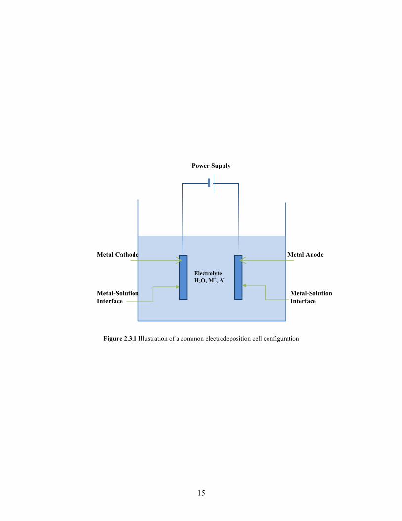
Figure 2.3.1 Illustration of a common electrodeposition cell configuration
Electrolyte H2O, M+, A-
Metal Cathode
Metal-Solution Interface
Metal Anode
Metal-Solution Interface
Power Supply
15
This process is reversible and will reach a balance resulting in the same concentration of 1.0×10-
14mol/L for both H+ and OH- ions at 25C. The ion-ion interaction in water is greatly affected by
its dielectric constant. According to the Coulomb Law, the potential of electrostatic interaction U
between two point charges q1 and q2 in a m ctric constant ε is given by: edium with diele
/ (2.18)
Since the dielectric constant of water is 78.5, the electrostatic interaction is greatly reduced
compared to that in a vacuum.
Two ways exists to form a solution by introducing ions in water. One method is by the
dissolution of ionic crystal (e.g., NaCl) which is composed of separate positive (Na+) and
negative (Cl-) ions. The overall dissolution process of an ionic crystal such as MA can be
represented as [40]:
(2.19)
This process consists of two steps: (1) separation of ions from the ionic crystal lattice and (2)
interaction of the ions with water molecules (hydration). Another method is the dissolution of a
potential electrolyte such as HA in water. The process can be represented as [40]:
(2.20)
The proton dissociated from the potential electrolyte HA (e.g. HOOCCOOH) will react with the
water molecule and form a hydronium ion H3O-. The difference between these two methods lies
in the fact that ionic crystals would form two separated ions while the latter forms hydronium
ions instead of separated and chemically unstable protons. The commonly used electrolytes for
metallic nanowire growth must fall in the first category since the positive ions are metallic ions
instead of protons.
16

2.3.2 Mechanisms of Electrodeposition of Metals
During the process of electrodeposition of metals, metal ions (Mn+) in the solution are transferred
into ionic metal lattices. The pro : cess can be represented as [40]
(2.21)
Since the metal ions in the solution are hydrated, as mentioned in the first case in section 2.3.1,
Mn+ should be replaced by [M(H2O)x]n+. Considering the atomic structure of a metal surface,
there exist different sites for the attachment of metal ions, such as terraces, step edges (ledges),
and kink sites. Kink sites are most favorable because of their lowest energy state. Thus, metal
ions would always like to sit at kink sites during their growth or deposition. As a result, equation
(2.21) should be represented 0 as [4 ]:
(2.22)
And this process can be completed via two different mechanisms: (1) step-edge site ion transfer
or (2) terrace site ion-transfer.
Step-edge site ion-transfer occurs when the ion-transfer proceeds at the kink sites or step-
edge sites. In either case, the metal ion is transferred from the solution into the kink sites at the
end. In the first case, the metal ions sit directly on the kink sites, while in the second case the
metal ion is transferred to the step-edge and diffuses along the step-edge until it finds the kink
sites. As a result, two possible paths for ion-transfer exist in step-edge site transfer: direct
transfer to kink sites and the step-edge diffusion path. In this mechanism, the metal ion would
lose half of its bonds with the water molecules but would bond with the metal surface. Thus, the
ion belongs to the bulk crystal.
17

Terrace ion-transfer mechanism, on the other hand, happens when a metal ion is
transferred from the solution into the flat face of the terrace region of the substrate surface. In
this position, the metal ion has most of its water molecules and bonds weakly with the bulk
crystal. But this position is not a stable one and the ion would diffuse on the surface seeking a
lower energy position. The final site is a kink site.
Metal ions in the solution would transfer into the crystal and sit at the lowest energy sites
- kink sites – either directly or through diffusion on the metal surface. These mechanisms formed
the basis of our design for nanowire growth in which we purposely fabricated lower energy sites
for metal ions deposition to confine the growth of the nanowire.
2.3.3 Nucleation and Growth Models of Electrodeposition Nucleation and growth are the two steps involved in the electrodeposition of metals. Nucleation
is the first step when initial nuclei sit on the surface of the substrate and form the basis of the
further growth of metal crystals. This process is highly dependent on the surface structure of the
substrate or, more specifically speaking, on how many nucleation sites exist on the substrate
surface. The nucleation law for a uniform probability with time t of conversion of a site on the
metal electrode into nuclei is given by [40]
1 (2.23)
where N0 is the total number of sites, and A is the nucleation rate constant. This equation
represents the first-order kinetic mo T 2D nucleation J is given by [40] del of nucleation. he rate of
/ (2.24)
where k1 is the rate constant, b is the geometric factor depending on the shape of the 2D cluster, s
is the area occupied by one atom on the surface of the cluster, ε is the specific energy, and k is
18

the Boltzmann constant. If the nucleation constant A is large, all electrode sites are
instantaneously converted to nuclei. If A is small, the number of nuclei N is a function of time t,
and the nucleation is progressive.
The growth of nuclei is another key step in electrodeposition. There are basically four
simple models of nuclei: (a) a two-dimensional cylinder; (b) a three-dimensional hemisphere; (c)
a right-circular cone; and (d) a truncated four-sided pyramid. The growth rate of a single 2
dimensional cylindrical nucleus and a single 3 dimensional hemispherical nucleus are given by
[40]
(2.25)
and (2.26)
respectively, where i represents the growth current, k is the rate constant, h is the height of a
nucleus, M is the molecular weight, and ρ is the density of deposit.
After the growth of a single nucleus, multiple nuclei might collide with each other,
leading to the formation of a monolayer. There can be two different mechanisms: (1) the
instantaneous nucleation mechanism according to which the monolayer is growing from the
nuclei formed instantaneously on the substrate in t=0; and (2) the progressive nucleation
mechanism in which nuclei appear randomly in space and time [40].
Once the monolayer is formed, the multilayer formation begins. There are two different
mechanisms: (1) monolayer layer-by-layer growth and (2) multinuclear multilayer growth. The
first mechanism happens when the overpotential applied is slightly higher than the critical
overpotential and when the nucleation rate is slower than the growth rate of nucleus. In this case,
each nucleus spreads over the entire surface before the next nucleus is formed. Therefore, the
19

growth occurs in a layer-by-layer mode. The second mechanism, however, happens at a higher
overpotential when the nucleation rate greatly increases. Because the growth of each monolayer
proceeds with the formation of many nuclei, this process is multinuclear.
A coherent deposit is formed after the completion of the growth of a number of
monolayers. Layer growth and 3-D growth are the two mechanisms for the formation of coherent
deposit. In the layer growth mechanism, a crystal grows by the lateral spreading of discrete
layers one after another; each growth layer is a structure component. In 3-D growth mechanism,
however, the coherent deposit is built by the coalescence of different 3-D crystallites which are
the structure components in the deposit formed on substrate.
Different structures of deposit can be formed under different growth conditions, such as
growth current or overpotential, which are directly related to the fact that the growth and
nucleation process is dependent on the overpotential during growth. A correlation found by
Seiter et al. between overpotential η and current density with corresponding growth forms of
electrodeposited copper on copper sheet substrate presented this fact: four structural forms of
copper: ridge, platelet, block, and polycrystalline existed and the higher the overpotential, the
more disordered the deposit would be. Finer structure was formed under small overpotential.
2.4 E-BEAM LITHOGRAPHY AND PMMA 2.4.1 PMMA: Properties and Application as Resist
Polymethylmethacrylate, abbreviated as PMMA, is a thermoplastic and transparent plastic.
Commonly referred to as acrylic glass, it is even clearer than normal glass and works as an
alternative to glass in many areas. Its molecular formula is (C5O2H8)n and its density is 1.19 H
20

g/cm³. It has a melting point of 130–140 °C and a spoiling point of 200.0 °C. Because PMMA’s
surface and volume resistivity are 1014 Ω/sq and 2−14×1015 Ω·cm, respectively, it is an insulator.
Although PMMA can be used for many imaging and non-imaging microelectronic applications,
its most common use is as a high resolution positive resist for direct electron beam as well as X-
ray and deep UV writing in microlithographic processes. Since PMMA has no sensitivity to
white light, it is very suitable for clean room or even lab environment use. Sometimes, PMMA is
also used as a protective coating for wafer thinning, such as a bonding adhesive, and as a
sacrificial layer.
Standard PMMA resist products cover a wide range of film thicknesses and are
formulated with 495,000 & 950,000 molecular weight (MW) resins in either chlorobenzene or
the safer solvent anisole. Depending on the solvent type and the weight percentage, PMMA resist
can be categorized as A2, A4, A6… C2, C4, C6… etc., “A” represents Anisole, “C” represents
Chlorobenzene, and the numbers (2, 4, 6…) represent the weight percentage of PMMA in
solution [41].
2.4.2 E-Beam Lithography: Fundamentals and Processes Electron beam lithography, often abbreviated as e-beam lithography or EBL, is the process in
which a patterned beam of electrons is scanned across a surface covered with a layer of resist
(such as PMMA), and either exposed (i.e. positive resist, PMMA) or non-exposed (negative
resist) regions of the resist are selectively removed. It is different from conventional photo
lithography in that its source is no longer UV light but electron beams with a much smaller
wavelength. A key advantage of e-beam lithography is that it is able to fabricate features within
nanometer range because of its small wavelength and small diffraction effect. Theoretically, the
21

minimum feature size it can achieve is only a few nanometers, but because of the proximity
effect, the resulted feature size is broadened. However, by using a proper process and resist, the
fabrication of structures with an aspect ratio of 10 with widths less than 40 nm can be
successfully done [42]. E-beam lithography is also more desirable for fabricating a specific
pattern within the nanometer scale since it is a maskless and point-to-point process. However,
EBL also suffers from long exposure time (~2hr/wafer) and low throughput.
The standard e-beam lithography process, including wafer cleaning, resist spin-on, pre-bake, e-
beam writing, development, and post-bake, resembles that of photolithography. For PMMA
resists, the post-bake is not necessary. Table 1 presents a recipe of a 100nm feature size e-beam
lithography process developed in our experiment. With this recipe, we were able to fabricate
channels with dimensions: 100 nm(Width)×150 nm(Depth)×30 µm(Length).
2.5 PALLADIUM AND HYDROGEN-PALLADIUM SYSTEM Palladium (Pd) is perhaps the most commonly used material in today’s applications related to
hydrogen, such as hydrogen sensors and hydrogen storage. When it comes to the nanotechnology
area, palladium thin films and mesowires or nanowires have been reported as effective hydrogen
sensors or switches [43, 14]. In this thesis, we use Pd as the material to fabricate single
nanowires and to study its response to hydrogen because of its unique properties.
2.5.1 General Properties of Palladium
Palladium is a soft silver-white metal that resembles platinum. Along with platinum, rhodium,
ruthenium, iridium, and osmium, palladium belongs to a group of elements referred to as the
22
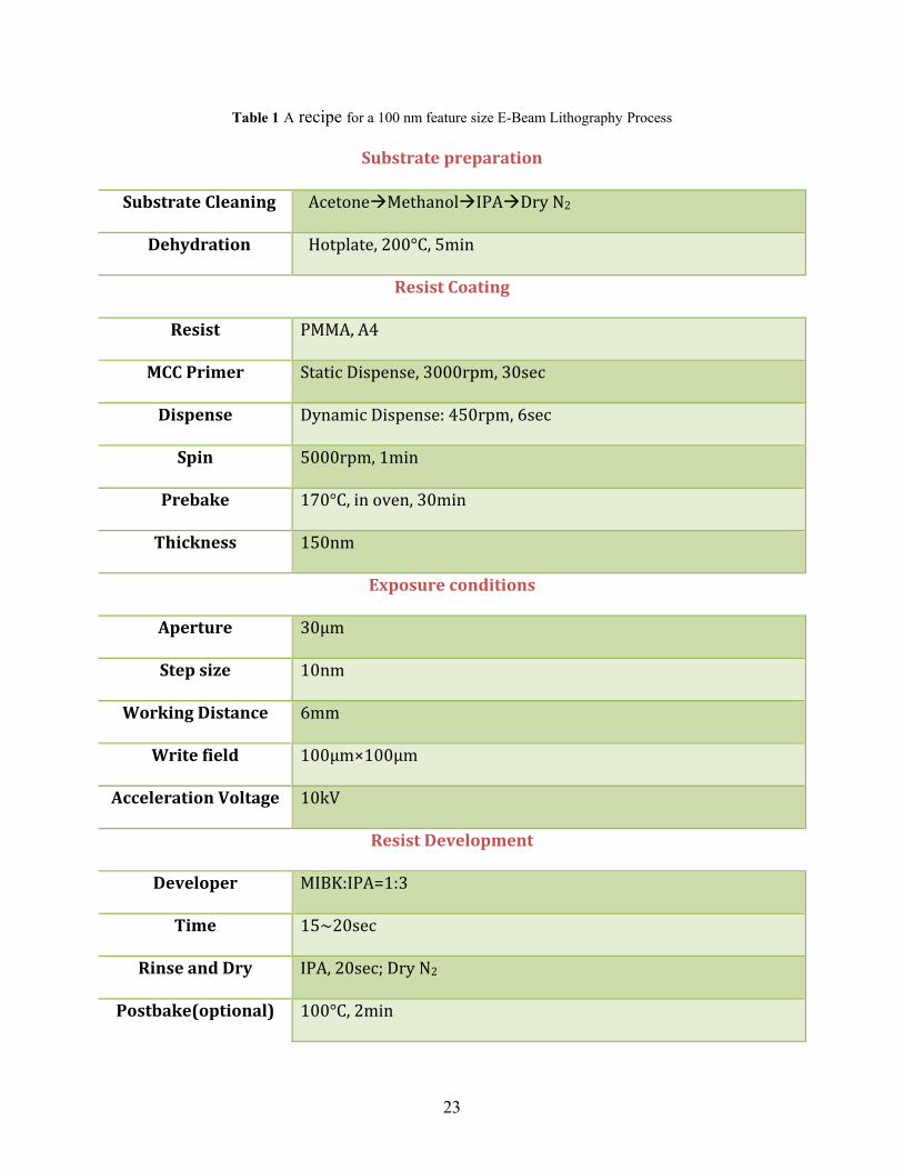
Table 1 A recipe for a 100 nm feature size E-Beam Lithography Process
Substrate preparation
Substrate Cleaning Acetone Methanol IPA Dry N2
Dehydration Hotplate, 200°C, 5min
Resist Coating
Resist PMMA, A4
MCC Primer Static Dispense, 3000rpm, 30sec
Dispense Dynamic Dispense: 450rpm, 6sec
Spin 5000rpm, 1min
Prebake 170°C, in oven, 30min
Thickness 150nm
Exposure conditions
Aperture 30µm
Step size 10nm
Working Distance 6mm
Write field 100µm×100µm
Acceleration Voltage 10kV
Resist Development
Developer MIBK:IPA=1:3
Time 15~20sec
Rinse and Dry IPA, 20sec; Dry N2
Postbake(optional) 100°C, 2min
23

platinum group metals (PGMs). It is the least dense in PGMs and has the lowest melting point.
Its basic properties are listed in Table 2. Among all the properties of Pd, the most appealing one
is its ability to absorb hydrogen. Palladium can absorb up to 900 times its own volume hydrogen
at room temperatures; this property is quite specific to only hydrogen. It is this property that
makes Pd the perfect media in hydrogen storage applications.
2.5.2 Hydrogen Palladium System
As mentioned above, Pd is selected as an important candidate in hydrogen related applications
because of its unique properties towards hydrogen. First of all, upon introduction of hydrogen
under room temperature, the chemical state of Pd changes [44]. As shown in Figure 2.5.1(A),
two different phases of palladium hydrides, including alpha (α) phase and beta (β) phase,
exist when hydrogen is introduced. At room temperature or higher temperatures, α phase Pd
hydride has a very low atomic ratio of H/Pd (<0.1), while β phase Pd hydride has a much higher
atomic ratio (H/Pd≈0.7). These two phases can coexist when the atomic ratio is in middle range.
Figure 2.5.1(B) shows that the composition of Pd changes accordingly with the hydrogen partial
pressure. Under certain environmental pressure and temperature, the higher hydrogen
concentration results in a higher hydrogen partial pressure. Thus, this figure indicates that the
phase of Pd hydrides formed is directly dependent on the actual concentration of hydrogen. With
lower hydrogen concentration (or partial pressure), the hydride would be α phase and β phase
hydride forms with higher hydrogen concentration. The transition from α phase to β phase is
reversible when the hydrogen concentration changes. Also, the relationship between the Pd
hydride composition and hydrogen pressure under different temperature has been studied in
detail [45] and used in sensor working temperature selection.
24

Table 2 Basic Properties of Palladium
Name/Symbol/Number Palladium/Pd/46
Group/Period/Block 10,5,d
Appearance Silvery white metallic
Standard Atomic Weight 106.42 g·mol‐1
Phase Solid
Density (room temperature) 12.023 g·cm−3
Crystal Structure Cubic face centered
Melting Point 1828.05K
Boiling Point 3236K
Electrical Resistivity 105.4 nΩ·m(20°C)
25

In accordance with the transition of the Pd hydride from α phase to β phase, two
detectable effects occur which form the basis of many hydrogen sensors. First of all, a resistance
increase occurs when the hydride shifts from α phase to β phase, as Figure 2.5.2 illustrates [46].
R0 represents the resistance of palladium when H/Pd is 0. R represents the actual resistance of Pd.
It is clear that the resistance change could be as high as 1.8 times at room temperature (solid
circles) when the Pd hydride transforms from α phase (H/Pd≈0) to β phase (H/Pd≈0.7).
Secondly, a structural lattice change would happen. Palladium has an fcc structure with a
lattice parameter of 0.3890 nm (298K). Upon hydrogen absorption, the lattice undergoes an
isotropic expansion while keeping its fcc structure. In α phase (298 K), the lattice parameter of
PdH~ is 0.3894 nm, which reflects its small component ratio of H/Pd (~ 0.015). However, in β
phase, which co-exists with α phase, the lattice parameter is 0.4025 nm where the component
ratio H/Pd is much higher (~0.7) [14, 44]. The volume expansion from α phase to β phase is
around 10.4% [14, 44, and 45]. This 10.4% volume expansion could be a dominant effect when
it comes to a nanosized structure.
Upon phase transition of PdH from α phase to β phase, the resistance would go up while the
lattice expands because of higher H/Pd ratio. These two effects form a basis of understanding the
mechanism of hydrogen sensors in the following parts.
26
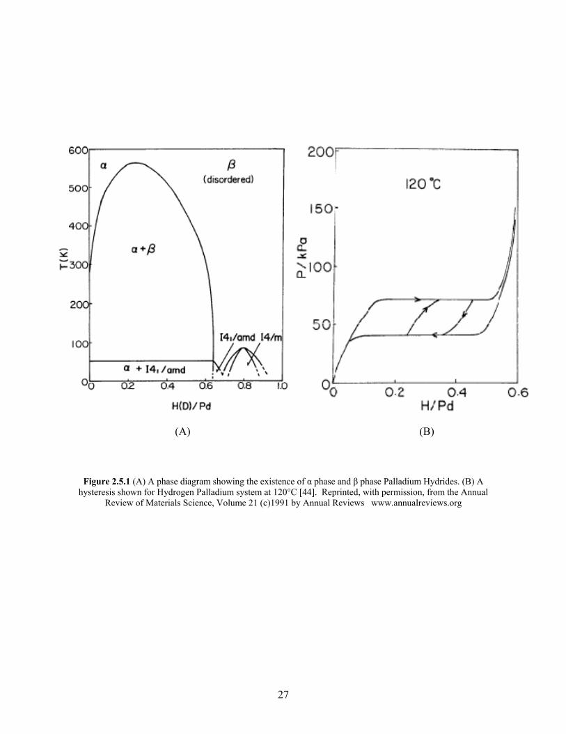
(A) (B)
Figure 2.5.1 (A) A phase diagram showing the existence of α phase and β phase Palladium Hydrides. (B) A hysteresis shown for Hydrogen Palladium system at 120°C [44]. Reprinted, with permission, from the Annual
Review of Materials Science, Volume 21 (c)1991 by Annual Reviews www.annualreviews.org
27

Figure 2.5.2 Relationships between H/Pd and R/R0. Hollow circle: 0°C; solid circle: 25°C; triangle: 50°C [46]-Reproduced by permission of The Royal Society of Chemistry.
.
28

3.0 EXPERIMENT
3.1 TEMPLATE PREPARATION AND NANOCHANNEL FORMATION
The key issue of our experiment is to discover how to fabricate thin and uniform Pd nanowires.
In order to fabricate nanowires with diameters less than 100nm, we used electrophoresis to
deposit Pd on a substrate with 100 nm wide channels which went across pre-patterned gold
electrodes so that an electric field could be applied. This template was prepared using
conventional microelectronic processes together with a lift-off step and an e-beam lithography
step. Figure 3.1.1 illustrates the complete process.
We chose a (100) p type Si wafer as the substrate. In step A, a certain thickness SiO2 is thermally
grown working as an insulation layer. Two different thicknesses have been used: 100 nm and
150 nm. In steps B and C, the pattern of Au/Ti electrodes is transformed using optical
lithography. In step D, a layer of 95nm thickness Au is deposited by e-beam evaporation. In
order to increase the adhesion of the Au layer on SiO2, a layer of 5nm Ti layer is deposited
before deposition of Au. Then, the patterned photoresist is removed using warm acetone and
Au/Ti electrodes are formed after lift-off. These electrodes will work as the conduction pads for
both electrophoresis and wire bonding. Nanochannel is formed in steps E and F. In step E, a
layer of 100 nm to 150 nm thick PMMA is spun on the substrate. After the e-beam lithography
steps, nanochannels with 100nm diameters are formed in step F. A detailed recipe for e-beam
lithography is shown in Table 2.5.1. The distance between electrode pads varies from 3 µm to 5
29

A B
GrowthSiO2Si SubstrategraphyPhotolitho
AuDeposition
OffLift − BeamE −yLithograph
D C
SiSiO2
Photo ResistPMMA
E FAu
Figure 3.1.1 Fabrication process of template for 100 nm PMMA channels. A: 100 nm thick SiO2 growth; B:
Photoresist spin-coating; C: Development of photoresist; D: E-beam evaporation of 5nm thick Ti layer as adhesion
layer followed by 95nm thick gold layer as electrode. E: PMMA spin-coating; F: E-beam lithography and
development of PMMA to pattern 100 nm wide nanochannels.
30

(A) (B)
Figure 3.1.2 (A) An AFM image of nanochannel together with electrodes on both sides. The size of the image is
8×8 µm2 and the channel length is 4.5 µm. (B) The 3-D view of the channel and electrodes. The height of the
electrode is 100 nm and the depth of the channel is 100 nm.
31

µm. These channels have a length of 20 µm going across the gap between the electrode pads.
Finally, a channel with two ends connected to Au/Ti electrodes and the upper side opened to air
is formed. Figures 3.1.2 A and B present AFM images showing the nanochannel between
electrodes.
3.2 SINGLE NANOWIRE DEPOSITION VIA ELECTROPHORESIS DEPOSITION
Once the fabrication process of the template wafer is finished, the wafer is cut into small slices
and ready for electrophoresis deposition.
3.2.1 Preparation of Electrolyte Solution The process of Pd deposition is completed by placing a drop of solution on the nanochannel and
applying an electric field through it. This electrolyte solution contains Pd(NH2)2(NO2)2
(Diamminepalladium Nitrite) and NH4SO3NH2 (Ammonia Sulfamate) with concentrations of
10g/L and 100g/L, respectively [47]. In the solution, the two components would go through the
following dissolution processes:
Pd NH NO Pd NH NO (3.1)
and
NH SO NH NH NH SO (3.2)
Thus, this solution contains Pd2+ which works as the Pd source in electrodeposition. During the
electrophoresis deposition process, the pH value of this solution is adjusted at around 7 by
32

adding H3NSO3 (sulfamic acid) and NaOH (sodium hydroxide) to avoid its reaction with Au
electrodes or PMMA. The conductivity of the solution made ranges from 450 µS/cm to 600
µS/cm.
3.2.2 Nanowire Growth The electrophoresis deposition of the Pd nanowire is finished in a probe station, as shown in
Figure 3.2.1. The probe station consists of four separate probes with 1 µm diameter tips. Via
coaxial cables, the probes are connected to a semiconductor analyzer (Agilent B1500A) which
supplies electrical signals and collects data. In our experiment, we attach two probes to the
electrodes on both sides of the channel. Then, we place a drop of Pd electrolyte solution (~0.5 µL)
on the channel using a micropipette. After that, a constant current (10nA~500nA) is applied
through the two probes; the voltage signals are collected and shown by semiconductor analyzer.
Figure 3.2.2 (a) illustrates this process. By monitoring the voltage drop across the channel, we
are able to tell whether the growth of the nanowire is completed. During the growth process, the
Pd nanowire grows from one electrode (cathode) to another (anode), but the two electrodes are
not connected. The expected voltage drop would be a few volts. Once the Pd nanowire connects
the other electrode (anode) and the growth is completed, the resistance between the two
electrodes drops dramatically; thus results in a sharp drop of the voltage signal, as shown in
Figure 3.2.2 (b). The voltage in this case is around 100 µV to a few mV. The current should be
stopped once the voltage drops to avoid further axial growth of the nanowire.
33
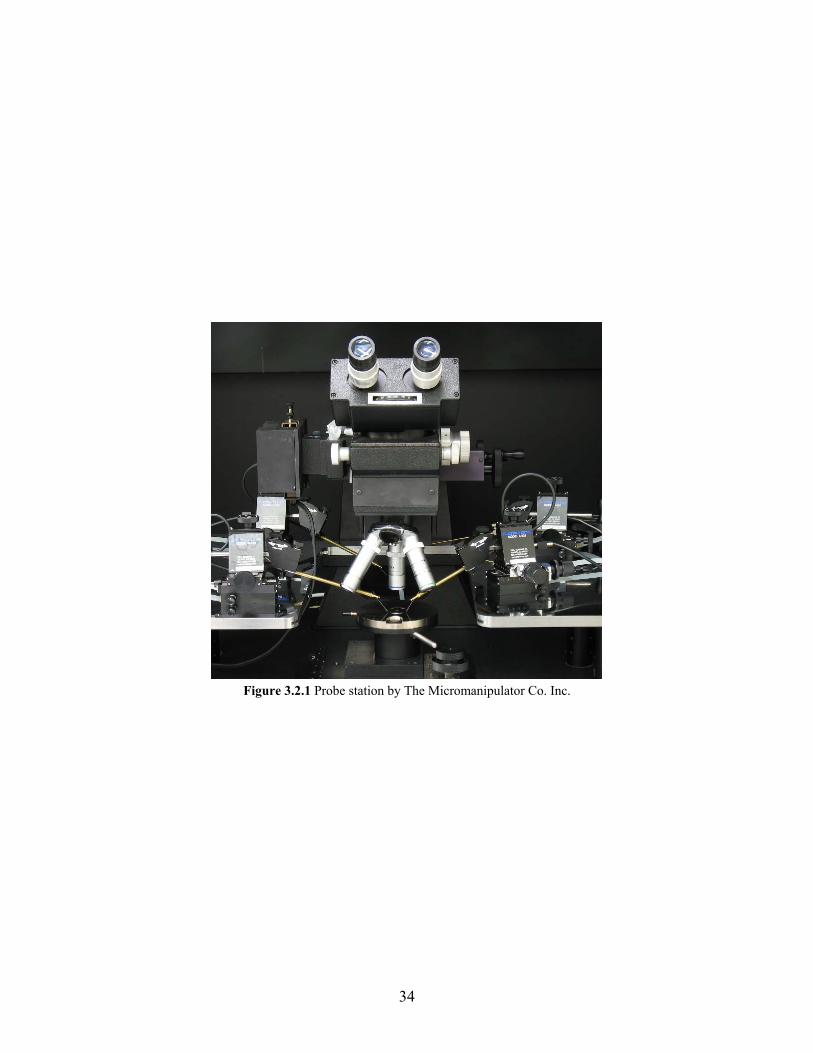
Figure 3.2.1 Probe station by The Micromanipulator Co. Inc.
34

Figure 3.2.2 (A) Two probes provide a constant current through the channel during growth. (B) Voltage drop
appears when nanowire growth is completed.
Analyzer
Time (s)0 5 10 15 20
Volta
ge (V
)
0
1
2
3
During Growth Growth Complete
(B) (A)
35

3.3 INTEGRATION OF SENSOR DEVICES
In order to use the nanowires in hydrogen sensing, we have to integrate single nanowires into
devices by adding external circuits. Wirebonding is the process of connecting the nanowire with
an external circuit by bonding the electrode pads into outer pins on a slice holder.
The wirebonding process is finished on a manual wedge wirebonder provided by Kulicke &
Soffa INC. The Au electrode pads are bonded by an Au wire with a 32 μm diameter through
which it is connected to a pin of a slice holder. The slice holder is bought from Aegis Inc. An
illustration of wirebonding and a finished device are shown in Figure 3.3.1 (a) and 3.3.1 (b),
respectively.
3.4 GAS SENSING SYSTEM SET-UP
Once the nanowire is wirebonded to the slice holder, a sensor device is finished. In order to
detect different concentrations of hydrogen, a gas sensing system, which is able to control the
gas concentration and apply and detect the electrical signal, is required.
The gas sensing system used in our experiments is illustrated in Fig. 3.4.1. First of all, a
Labview (National Instrument Inc., USA) program is built to control two gas lines, supplying
hydrogen gas and nitrogen gas, respectively, via an MKS flow controller system (MKS Multi
Gas Controller 647C, MKS Instruments Inc., USA). There are two different hydrogen gas
sources. The first one is 10% hydrogen, and the second is manufacture certified 0.1% hydrogen
with nitrogen gas as a balance gas (Matheson Tri Gas Inc., USA). To achieve the desired
36

(A)
(B)
Figure 3.3.1 (A) Illustration of a sensing device with wirebonded nanowire. (B) A real image of sensing fabricated
sensor device.
37
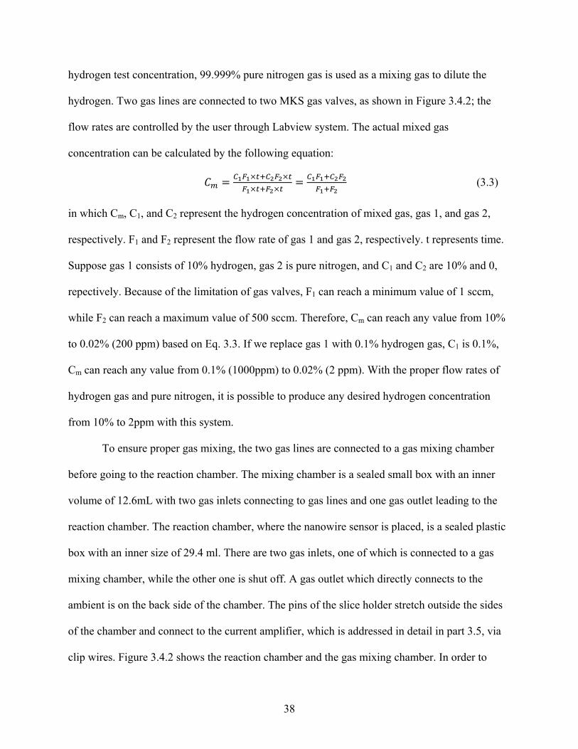
hydrogen test concentration, 99.999% pure nitrogen gas is used as a mixing gas to dilute the
hydrogen. Two gas lines are connected to two MKS gas valves, as shown in Figure 3.4.2; the
flow rates are controlled by the user through Labview system. The actual mixed gas
concentration can be calculated by the following equation:
(3.3)
in which Cm, C1, and C2 represent the hydrogen concentration of mixed gas, gas 1, and gas 2,
respectively. F1 and F2 represent the flow rate of gas 1 and gas 2, respectively. t represents time.
Suppose gas 1 consists of 10% hydrogen, gas 2 is pure nitrogen, and C1 and C2 are 10% and 0,
repectively. Because of the limitation of gas valves, F1 can reach a minimum value of 1 sccm,
while F2 can reach a maximum value of 500 sccm. Therefore, Cm can reach any value from 10%
to 0.02% (200 ppm) based on Eq. 3.3. If we replace gas 1 with 0.1% hydrogen gas, C1 is 0.1%,
Cm can reach any value from 0.1% (1000ppm) to 0.02% (2 ppm). With the proper flow rates of
hydrogen gas and pure nitrogen, it is possible to produce any desired hydrogen concentration
from 10% to 2ppm with this system.
To ensure proper gas mixing, the two gas lines are connected to a gas mixing chamber
before going to the reaction chamber. The mixing chamber is a sealed small box with an inner
volume of 12.6mL with two gas inlets connecting to gas lines and one gas outlet leading to the
reaction chamber. The reaction chamber, where the nanowire sensor is placed, is a sealed plastic
box with an inner size of 29.4 ml. There are two gas inlets, one of which is connected to a gas
mixing chamber, while the other one is shut off. A gas outlet which directly connects to the
ambient is on the back side of the chamber. The pins of the slice holder stretch outside the sides
of the chamber and connect to the current amplifier, which is addressed in detail in part 3.5, via
clip wires. Figure 3.4.2 shows the reaction chamber and the gas mixing chamber. In order to
38
Voltage Source
Gas Controller
Gas valve
AData Acquisition system
Current amplifier
Mixing
Nanowire
Reaction Chamber
Gas valve
Figure 3.4.1 Sensing system set-up
39

Figure 3.4.2 Reaction chamber (left) and gas mixing chamber (right).
40

reduce the effect of ambient noises, the sensing chamber is placed inside a metallic box which
works as a Faraday cage. The sensing system does not require a pumping system and is operated
at room temperature.
3.5 SIGNAL COLLECTION AND PROCESSING
In order to detect the resistance change of nanowires during hydrogen sensing, a constant DC
voltage (~2.5 mV) is applied to the nanowire via a current amplifier (Keithley 428 Current
Amplifier). This further collects the current signal running through the nanowire and converts it
into a voltage signal proportional to the current signal. The output of the current amplifier is the
converted voltage signal but with 103 to 107 amplification. This output signal is then connected
with a data acquisition system (Keithley 2701) and recorded by Labview program. The final
sensing chart based on collected data is plotted using a plotting software (Sigma Plot 9).
41
4.0 RESULTS AND DISCUSSION
4.1 NANOWIRE GROWTH AND PROPERTIES By using electrophoresis deposition, we were able to successfully and constantly fabricated Pd
single nanowires with diameters ranging from 50 nm to 100 nm. In order to study the surface,
electrical, and structural properties of nanowires, we used a Semiconductor Analyzer, Optical
and Scanning Electron Microscopy (SEM), and Atomic Force Microscopy (AFM) as
characterization instruments.
After a nanowire is grown on the slice, it is cleaned by gently washing it in Deionized (DI)
Water and then dried using pure dry nitrogen gas. An image of the channel and nanowire is taken
using optical microscope (Carl Zeiss AG Reflected-Light Microscope) to verify the growth. An
optical image with a magnification of 150×10 times is shown in Figure 4.1.1. As seen in the
image, a channel formed by PMMA crosses both electrodes. PMMA is not clearly seen because
it is very thin and clear. The nanowire is the dark tiny line inside the channel which can be barely
seen. Since the maximum magnification is 1500 times, the diameter (~100 nm) is too small to be
observed.
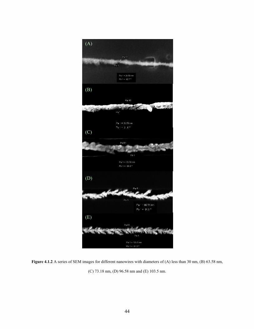
In order to further study the surface properties, an SEM system (Raith e-line) is used to
take clearer images of the nanowires. The diameter of the nanowire ranges from less than 50 nm
to over 100nm. A series of SEM images presented in Figure 4.1.2 show different nanowires with
different diameters.
42

Figure 4.1.1 An optical image with 150×10 times magnification of a grown nanowire. There are two pairs of
electrodes (yellow) and two channels (tiny lines between the electrodes). The nanowire grown, which is in the
bottom channel, can be barely seen.
43
(A)
(B)
(C)
(D)
(E)
Figure 4.1.2 A series of SEM images for different nanowires with diameters of (A) less than 30 nm, (B) 63.58 nm,
(C) 73.18 nm, (D) 96.58 nm and (E) 103.5 nm.
44
(A) (B)
(C)
Figure 4.1.3 (A) An AFM image of a grown nanowire with 100 nm width and 6.5 µm length between electrodes. (B)
A 3-D view of the nanowire and electrodes on both sides. (C) A line profile shows the height of the nanowire at
around 74 nm.
45

AFM is used to detect the morphology of the nanowires. The nanowires are grown inside
the PMMA channels with 100 nm thickness (as shown in Figures 3.1.2 A and B); thus, it is
difficult to directly detect the nanowires using AFM because of the existence of PMMA.
Because of this, we gently dipped our samples into warm (45°C) acetone for 5-10 minutes to
remove the PMMA. After proper cleaning and drying, the nanowire is exposed on the surface
and ready for AFM scan. In order not to damage the nanowire during scanning, a tapping mode
is used. The AFM images of a grown nanowire are shown in Figure 4.1.3. Figures 4.1.3 A and B
illustrate that the nanowire grown is very uniform in both width and height. The measured height
of the nanowire from Figure 4.1.3 C is 74 nm, quite consistent with the 100 nm PMMA thickness.
The electrical resistance of the nanowire is tested using a semiconductor analyzer. As
metallic material, the Pd nanowire shows a clear linear resistance over a range of voltage (from
−3 mV to 3mV); resistances ranging from 100 Ω to over 10,000 Ω have been measured. The
actual resistance of the nanowire primarily depends on three factors: physical dimensions,
nanowire structures, and the connection between the nanowire and electrodes.
Physical dimensions refer to the diameter and length of the nanowire. Indicated by
classical conductance law (Eq. 2.5), the nanowire’s resistance is proportional to its length and
inversely proportional to its cross-sectional area. However, our experiments showed only a weak
connection not a clear trend that conforms to the law between resistance and length or diameter
of nanowires. We attribute this to the fact that resistance also relies heavily on other factors.
The second factor is the actual structure of the nanowire. Nanowires grown are not ideal
cylinders but have grain structures. They are neither really uniform in diameter nor in grain sizes.
How the grains are grown and how well they connect with each other affects the actual resistance
of the nanowires. The resistance of a nanowire is decided by its critical sites, such as the
46

narrowest part and the points where two grains connect to each other. This is the major reason
why nanowire resistance does not conform to the classical law.
The connection between the nanowire and electrodes, especially the anode, is also critical.
As the nanowire grows from cathode to anode, the growth process ends when the nanowire
touches the anode. The connection could be very weak since the contact area between nanowire
and electrode pad could be around, or even smaller than, grain size. Furthermore, there could be
residual PMMA on both ends of the channel which stops the nanowire from fully connecting
with the electrode pads. In order to have a good sensor performance, the nanowire must be kept
in close and ohmic contact with the electrode pads so that the resistance change depends on the
nanowire itself.
4.2 NANOWIRE STRUCTURES AND GROWTH CONTROL As mentioned in part 4.1, a nanowire has different structures depending on the size of grains and
how they connect together. In our experiments, we found three different kinds of nanowire
structures: (1) plain structure, (2) grain structure, and (3) hairy structure. SEM images of these
structures are shown in Figure 4.2.1 A to F. Plain structure nanowires, as shown in Figure 4.2.1
A and B, are composed of very tightly bound particles that are well connected to each other with
no gaps. The diameter of this kind of nanowire is relatively uniform along the channel, and the
surface is relatively plain. The grains in this structure are very well grown and connected. The
grain structure nanowires, however, consist of small nano-sized grains, each barely connected to
the others by a very small neck, as shown in Figures 4.2.1 C and D. The diameter of this kind of
nanowire varies along the channel; the neck part can be as small as 10 nm or 20 nm. The typical
47
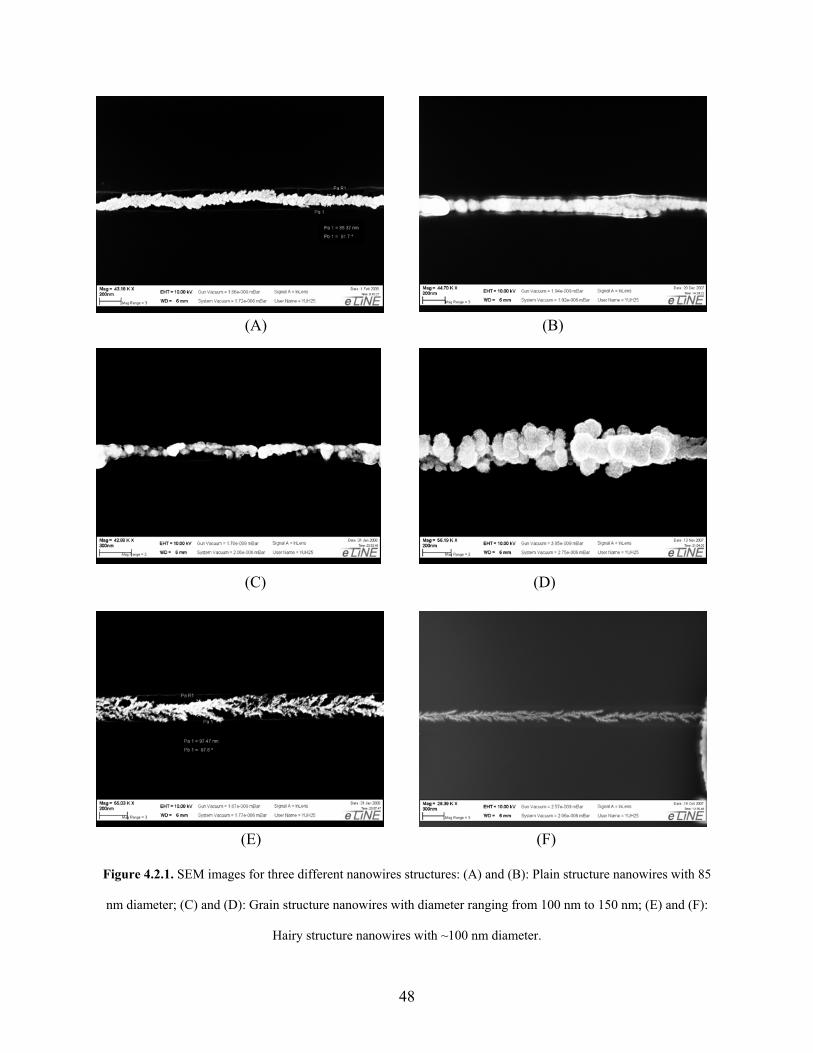
(A) (B)
(C) (D)
(E) (F)
Figure 4.2.1. SEM images for three different nanowires structures: (A) and (B): Plain structure nanowires with 85
nm diameter; (C) and (D): Grain structure nanowires with diameter ranging from 100 nm to 150 nm; (E) and (F):
Hairy structure nanowires with ~100 nm diameter.
48

size of individual grains or nodes ranges from 50 nm to100 nm. The grains in this structure are
either not fully grown or too far apart from each other so that they barely connected each other.
Hairy structure nanowires, shown in Figures 4.2.1 E and F, are similar to a tree structure. They
have a trunk in the center and many dendrite-like branches reaching outward. The length of
individual branches is limited by the width of the channel. In this structure, the grains are very
small and the growth is very fast.
Through extensive experiments, we found that the structure of the nanowire is closely
related to the electric field and current during growth. Based on this, we were able to control the
actual structure of the nanowire. In these tests, the same 6 μm length and 100 nm width channels
were used, while the growth current was varied. As shown in Figures 4.2.2 A to C, three SEM
images with three different growth currents of 500 nA (A), 100 nA (B), and 50 nA (C) indicate a
clear relationship between current and nanowire structure. With a higher current (Figure 4.2.2 A),
the nanowire tends to grow fast, produce more dendrites, and form a hairy structure. With a
lower current (Fig.4.2.2 C), the growth is comparatively slower and produces a grain structure.
Interestingly, with an intermediate current, the nanowire could show grain structure on the
cathode (left) side and hairy structure on the anode (right) side, as shown in Fig. 4.2.2 B.
A possible explanation could be reached by considering the deposition as a combined
process of grain growth and electric field driven aggregation. During electro deposition, the
grains already deposited are growing, while metal ions are driven by the electric field and
attaching to the tip of grown nanowire, as shown in Figure 4.2.3. When a higher current is
applied, the electric field in the channel is higher and the aggregation of metal ions is much faster
than grain growth. Thus, the shape of the nanowire resembles that of diffusion limited
aggregation [48] and the grains are notably smaller. While the current is smaller, a smaller
49

(B)
(A)
(C)
Figure 4.2.2 SEM images for nanowires grown using three different currents: (A) 500nA growth current; (B)
100nA growth current. The upper left inset is a magnification of the left side, and the bottom right inset is a right
side magnification; and (C) 50nA growth current.
50
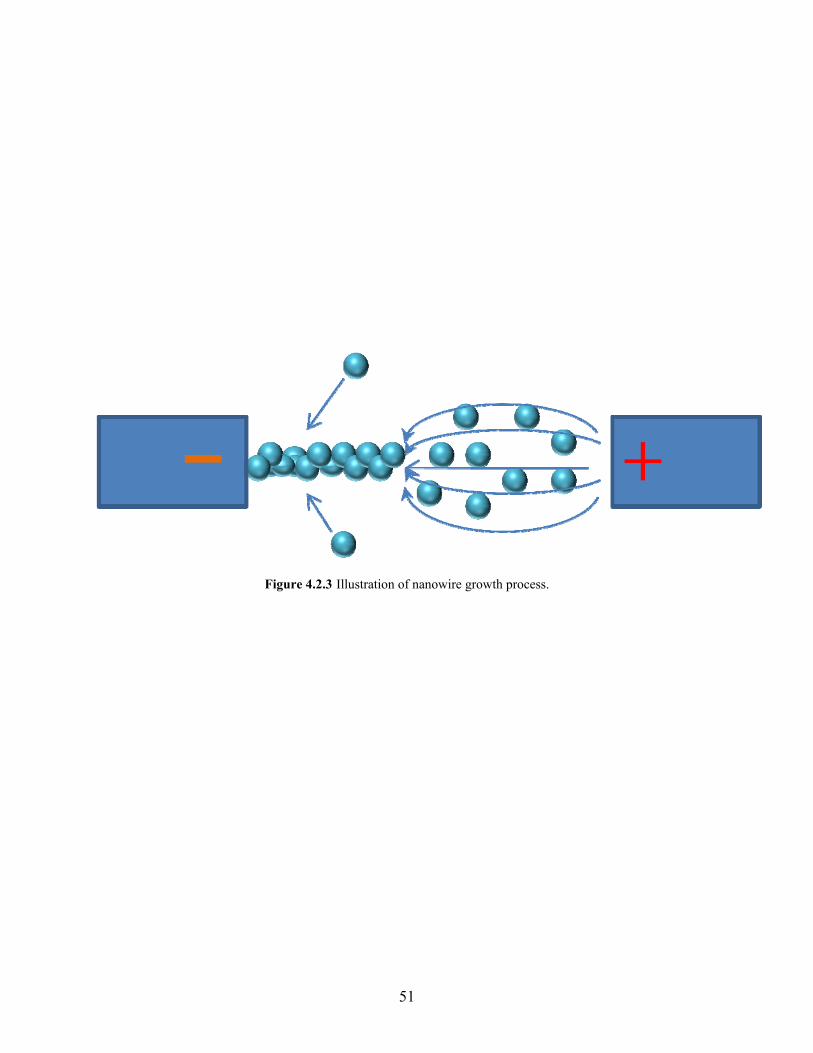
Figure 4.2.3 Illustration of nanowire growth process.
51

electric field is presented inside the channel. The grain growth is more favored as the nanowire
grows slowly from cathode to anode. In this case, a nanowire with the grain structure is formed.
With an intermediate current, the electric field inside the channel is small in the early stage of
nanowire growth since the distance from the nanowire tip to the anode is large. Therefore grain
growth is dominant in this stage when the nanowire grows from the cathode and the grain
structure is forms in the cathode side. Since Pd itself is metallic and a good conductor, the
electric field gets stronger and stronger between the nanowire tip and anode when the nanowire
grows close to the anode. In this stage, growth speeds up and the hairy structure forms in the
anode side. By setting a proper value of current using semiconductor analyzer, the structure of
nanowires can be controlled.
4.3 HYDROGEN SENSING: PERFORMANCES AND MECHANISMS
The performance of a sensor can be characterized by the following factors: sensitivity,
repeatability, and time. A great deal of hydrogen sensing of different hydrogen concentrations
using fabricated naonwire sensors have been conducted and studied in detail.
(1) Sensitivity. The sensitivity of our devices is ultra high with a maximum value of 2-5 ppm.
This value is the best sensitivity ever achieved using pure palladium and much better than
similar hydrogen sensors made by Pd nanowire arrays [14] and Pd nanowire bundles
[15].Figure 4.3.1 shows the sensing signal with 5ppm sensitivity. As indicated in the
graph, when hydrogen is introduced into the sensing chamber, the voltage converted by
the amplifier and collected by a data acquisition system showed a sharp increase. During
the test, different hydrogen concentrations were introduced into the chamber, following a
52
1000 ppm – 100 ppm – 50 ppm – 20 ppm – 10 ppm – 5 ppm – 2 ppm – 1000 ppm – 100
ppm – 10 ppm – 5 ppm – 2 ppm manner. It is clear that the sensor is not only able to
detect hydrogen with concentrations ranging from 10,000 ppm (1%) to 5 ppm (0.0005%)
consistently, but it can also discriminate different concentrations with different signal
heights.
(2) Repeatability. Repeatability, a key issue in sensor performance, characterizes the stability
and reliability of a sensor. Our devices showed a very good repeatability during hydrogen
detection, as shown in Figure 4.3.1 and Figure 4.3.2. In Figure 4.3.1, the sensing is
repetitive, and the signal height is constant for the same hydrogen concentrations. In
Figure 4.3.2, a sensing result with a same hydrogen concentration is presented. It is
obvious that for the same hydrogen concentration (5000 ppm), the sensing is very
repetitive with a fairly constant signal height. These results prove that the repeatability of
our nanowire sensor devices is good. It should be noted, however, that the background
signal of our devices has a certain drift. This drift could result from either hydrogen
accumulation on the nanowire surface during sensing or the thermo effect of nanowire
resistance. The drift undermines the reliability of devices and requires further research.
(3) Response time. Response time, which shows how quickly a sensor reacts to
environmental change, can be characterized by rise time, which is defined as the time
required for the sensor output to change from its initial state (10% value change) to a
final value (90% value change). Fast response is critical in hydrogen detection, especially
in aircrafts and spaceships where hydrogen leakage is quick and fatal. The single
nanowire sensor devices in this work showed a good response time ranging from 9
seconds to a few tens of seconds. The real response time is even faster considering the
53
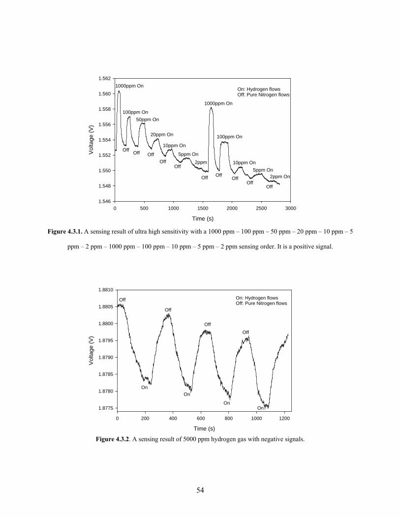
Time (s)
0 500 1000 1500 2000 2500 3000
Vol
tage
(V)
1.546
1.548
1.550
1.552
1.554
1.556
1.558
1.560
1.562
On: Hydrogen flows Off: Pure Nitrogen flows
1000ppm On
100ppm On50ppm On
20ppm On
10ppm On
5ppm On
1000ppm On
100ppm On
10ppm On5ppm On
2ppm
2ppm On
Off Off OffOff
Off
Off OffOff
OffOff
Figure 4.3.1. A sensing result of ultra high sensitivity with a 1000 ppm – 100 ppm – 50 ppm – 20 ppm – 10 ppm – 5
ppm – 2 ppm – 1000 ppm – 100 ppm – 10 ppm – 5 ppm – 2 ppm sensing order. It is a positive signal.
Time (s)
0 200 400 600 800 1000 1200
Vol
tage
(V)
1.8775
1.8780
1.8785
1.8790
1.8795
1.8800
1.8805
1.8810
On: Hydrogen flowsOff: Pure Nitrogen flows
Off
Off
OffOff
OnOn
OnOn
Figure 4.3.2. A sensing result of 5000 ppm hydrogen gas with negative signals.
54

Figure 4.3.3. A sensing result of 1% hydrogen with positive signal. The rise time is around 19 seconds.
Time (s)
350 360 370 380 390
Volta
ge (V
)
1.558
1.559
1.560
1.561
1.562
19.01 sec
Time (s)
ON ON ON
OFF OFF OFF1% Hydrogen sensing
100 200 300 400
1.558
1.559
1.560
1.561
1.562
Volta
ge (V
)
55

diffusion time from the tank to the sensing chamber. As shown in Figure 4.3.3, a 1%
hydrogen sensing shows a response time of roughly 19.01 seconds and proves the fast
response of single nanowire sensors.
In addition to the basic studies of hydrogen sensors, a new phenomenon was discovered
during the tests. Rather than reacting to hydrogen in the same way, the different nanowire
sensors showed diverse manners of resistance change upon the introduction of hydrogen. Taking
a closer look at Figure 4.3.1 and Figure 4.3.2, the signal change directions of the two nanowires
differ when hydrogen is presented. In the former graph, the voltage signal presents a sharp
increase when hydrogen is introduced; this means a decrease of resistance happens. In the latter
one, however, a sharp decrease of the voltage is presented, indicating an increase of nanowire
resistance when hydrogen is presented. This phenomenon reveals that sensing mechanisms of Pd
nanowires could be different, even if they are fabricated in the same way.
In order to fully address this issue, detailed research based on three different structures has
been conducted. As mentioned in part 2.4.2, two effects could happen to Pd nanowires when
exposed to hydrogen: resistivity increase and volume expansion. Because volume expansion
often results in an increase of contact area between grains, a decrease of resistance occurs. For
easier discussion, we call the voltage increase (or resistance decrease) during hydrogen exposure
a positive signal, since the voltage goes up. The voltage decrease (or resistance increase) is
called a negative signal since the voltage goes down. The two opposite effects work together
with the final direction of resistance change depending on the dominant effect.
For the plain structure nanowires, measurements showed negative signals when exposed to
hydrogen. The original resistance was recovered after nitrogen purged the sensing chamber. An
SEM image of a plain structure nanowire is shown in Figure 4.3.4; its sensing signal of 5000
56

ppm hydrogen is shown in Figure 4.3.2. The diameter of the nanowire approximated 100 nm; the
voltage drops (or nanowire resistance increases) when exposed to hydrogen. This can be
explained by considering the two effects together. Upon a phase change from α phase to β phase,
Pd (PdHx) shows a resistivity increase of 1.8 times, which would result in 180% increase of
resistance. The size expansion (3.36% lattice constant expansion), however, would result in a
contact area increase of 6.8%, decreasing the resistance of the nanowire by 6.8% at the most,
according to Eq. 2.5. It is obvious that resistivity change is dominant and the final trend is a
resistance increase, thereby causing a negative signal to appear.
For the grain structure nanowires, positive signals were mostly seen in the sensing tests. Also,
grain structure nanowires were found to have the highest sensitivity. The sensing signal in Figure
4.3.1 is a positive one; as shown in Figure 4.3.5, the nanowire used in this device has a grain
structure. This nanowire has many tiny contact areas (necks) between two grains. The size of
each neck is from less than 20 nm to 50 nm, and the grain size is from 50 nm to 100 nm. Because
of its special structure, the volume expansion effect becomes more important than resistance
change. Resistivity change still results in a 180% increase of resistance, while the volume
expansion results in a more resistance decrease compared to the plain structure. In Figure 4.3.5,
the green boxes are magnified images of grain structures in the nanowire. Consider a pair of
grains together with a tiny neck between them. Two causes of size expansion of the neck area
exist: 6.8% increase because of its own 3.36% lattice expansion; and a much bigger increase
because of the compression from neighboring grains. Since the sizes of the grains are 50 nm to
100 nm and the size of the neck is typically 20 nm to 30 nm, the volume expansion of the
neighboring grains has a strong impact on the neck. It forms an impressive stress which pushes
the neck from both sides and greatly increases the contact area. An illustration of this mechanism
57

Figure 4.3.4 SEM image of a plain structure nanowire with a negative signal. This nanowire has a diameter of 100
nm and length of 6.5µm.
Figure 4.3.5 SEM image of a grain structure nanowire with a positive sensing signal. This nanowire has a diameter
from around 150 nm to less than 30 nm; its sensitivity is 5 ppm.
58

Figure 4.3.6. An illustration of the sensing mechanism of positive signals. The left side picture shows the change of
neighboring grains and the size change on the neck. The right side picture shows the magnified view of the neck
structure.
59

Time(s)
100 200 300 400 500
Volta
ge (V
)
0.186
0.187
0.188
0.189
0.190
0.191On: Hydrogen flowsOff: Pure Nitrogen flows
OffOffOff
On On
60
(B)
(A)
Time(s)
500 1000 1500 2000 2500 3000
Vol
tage
(V)
0.533
0.534
0.535
0.536
0.537
On: Hydrogen flowsOff: Pure Nitrogen flows
On
Off
On
Off
On
Off
On
(D)
(C)
Figure 4.3.7. (A) SEM image of a hairy structure nanowire. (B) 1% sensing signal of nanowire A. (C) SEM image
of another hairy structure nanowire. (D) 1% sensing signal of nanowire C.

is shown in Figure 4.3.6. Upon the introduction of hydrogen, the above two effects join together
and result in a large increase of the contact area between neighboring grains, resulting in a big
decrease of resistance. The area increase, which can be a few times larger than the 180%
resistivity change, caused a positive signal to appear.
The hairy structure has a more complicated sensing mechanism than those of the plain
structure and grain structure. Interestingly, above mentioned two different sensing signals both
can happen in hairy structure nanowires. Figures 4.3.7 A to D present SEM images of two
different hairy structure nanowires and their corresponding sensing signals. In Figures 4.3.7 A
and C, two different hairy structure nanowires are shown. Their structures differ from each other.
Nanowire A has a clear trunk with fewer dendrites which are far apart from each other, while
nanowire C has no clear trunk but does have many dendrites which twist together with very
small gaps. Figures 4.3.7 B and D illustrate their sensing signals. Nanowire A has a negative
sensing signal, while nanowire C has a positive one. The presence of two different sensing
mechanisms can be explained as follows: In nanowire A, the volume change of the nanowire
does not add more contact area than plain structure nanowires since the dendrites are too far
apart and the gaps between them cannot be closed with 10.4% size expansion. In this case,
resistivity change is dominant, causing nanowire A act in a similar way to that of a plain
structure nanowire. In nanowire C, however, far more dendrites exist with smaller gaps between
them. Upon exposure to hydrogen, the size expansion of dendrites connects them and results in a
larger contact area, similar to that of grain structure nanowires. Thus, a positive signal appears in
this case.
61

Therefore, two different sensing signals have been found, and possible mechanisms have
been proposed for the three different nanowire structures. More detailed research is needed,
though, to fully address the structural and electrical change of the Pd nanowire upon exposure to
hydrogen.
4.4 GATE ASSISTED NANOWIRE GROWTH
Pd single nanowires with a 100 nm diameter or less have been successfully and repeatedly
fabricated using the electrophoresis deposition method described above. Their function as an
effective and ultra sensitive hydrogen sensor has been approved by integrating them into sensing
circuits. However, a more effective fabrication method, with a much higher success rate, a
shorter growth time (higher throughput), and a better nanowire structure (more uniform, etc), is
needed to further improve this process and demonstrate its promising future.
Rather than merely applying a one directional electric field to grow nanowire, we propose
a new idea of adding another electric field to assist and control the growth. This other electric
field is applied from an external electrode on the sample surface through the silicon substrate to
the channel, forming a back-gate-like structure as shown in Figure 4.4.1. In order to fabricate the
Au gate, we add an extra photolithography step before Au deposition. In this step opening areas
were patterned and etched on SiO2. These opening areas will be further deposited with gold
which will work as gate. Three probes are used in this configuration: Probes A and B, like the
previous configuration, connect to a DC current for nanowire growth. Probe C is the extra probe
on which a constant DC gate voltage (Vg) is applied. The effect of the extra gate voltage on the
nanowire growth inside the channel needs to be considered. Band diagrams and the distribution
62
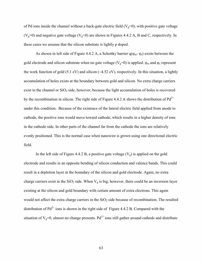
of Pd ions inside the channel without a back-gate electric field (Vg=0), with positive gate voltage
(Vg>0) and negative gate voltage (Vg<0) are shown in Figures 4.4.2 A, B and C, respectively. In
these cases we assume that the silicon substrate is lightly p doped.
As shown in left side of Figure 4.4.2 A, a Schottky barrier q(φm- φs) exists between the
gold electrode and silicon substrate when no gate voltage (Vg=0) is applied. φm and φs represent
the work function of gold (5.1 eV) and silicon (~4.52 eV), respectively. In this situation, a lightly
accumulation of holes exists at the boundary between gold and silicon. No extra charge carriers
exist in the channel or SiO2 side, however, because the light accumulation of holes is recovered
by the recombination in silicon. The right side of Figure 4.4.2 A shows the distribution of Pd2+
under this condition. Because of the existence of the lateral electric field applied from anode to
cathode, the positive ions would move toward cathode, which results in a higher density of ions
in the cathode side. In other parts of the channel far from the cathode the ions are relatively
evenly positioned. This is the normal case when nanowire is grown using one directional electric
field.
In the left side of Figure 4.4.2 B, a positive gate voltage (Vg) is applied on the gold
electrode and results in an opposite bending of silicon conduction and valence bands. This could
result in a depletion layer at the boundary of the silicon and gold electrode. Again, no extra
charge carriers exist in the SiO2 side. When Vg is big, however, there could be an inversion layer
existing at the silicon and gold boundary with certain amount of extra electrons. This again
would not affect the extra charge carriers in the SiO2 side because of recombination. The resulted
distribution of Pd2+ ions is shown in the right side of Figure 4.4.2 B. Compared with the
situation of Vg=0, almost no change presents. Pd2+ ions still gather around cathode and distribute
63
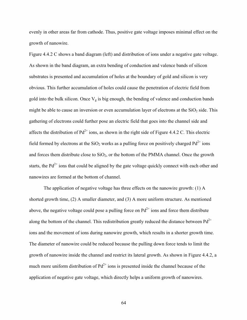
evenly in other areas far from cathode. Thus, positive gate voltage imposes minimal effect on the
growth of nanowire.
Figure 4.4.2 C shows a band diagram (left) and distribution of ions under a negative gate voltage.
As shown in the band diagram, an extra bending of conduction and valence bands of silicon
substrates is presented and accumulation of holes at the boundary of gold and silicon is very
obvious. This further accumulation of holes could cause the penetration of electric field from
gold into the bulk silicon. Once Vg is big enough, the bending of valence and conduction bands
might be able to cause an inversion or even accumulation layer of electrons at the SiO2 side. This
gathering of electrons could further pose an electric field that goes into the channel side and
affects the distribution of Pd2+ ions, as shown in the right side of Figure 4.4.2 C. This electric
field formed by electrons at the SiO2 works as a pulling force on positively charged Pd2+ ions
and forces them distribute close to SiO2, or the bottom of the PMMA channel. Once the growth
starts, the Pd2+ ions that could be aligned by the gate voltage quickly connect with each other and
nanowires are formed at the bottom of channel.
The application of negative voltage has three effects on the nanowire growth: (1) A
shorted growth time, (2) A smaller diameter, and (3) A more uniform structure. As mentioned
above, the negative voltage could pose a pulling force on Pd2+ ions and force them distribute
along the bottom of the channel. This redistribution greatly reduced the distance between Pd2+
ions and the movement of ions during nanowire growth, which results in a shorter growth time.
The diameter of nanowire could be reduced because the pulling down force tends to limit the
growth of nanowire inside the channel and restrict its lateral growth. As shown in Figure 4.4.2, a
much more uniform distribution of Pd2+ ions is presented inside the channel because of the
application of negative gate voltage, which directly helps a uniform growth of nanowires.
64

Figure 4.4.1 Illustration of gate-assisted nanowire growth set-up. A, B, and C represent three different probes that
connect to the semiconductor analyzer. Probes A and B connect to growth current, while probe C connects to a
constant DC voltage as a gate.
65

Figure 4.4.2 Band diagrams of the back gate structure (left) and illustrations of Pd2+ particles during growth (right)
with (A) Vg = 0, (B) Vg > 0, and (C) Vg < 0.
(A)
(B)
(C)
EF
Vg = 0
q(φm-φs)
Back gate Si SiO2
Vg > 0
q(φm-φs)
EF
-qVg
Vg < 0
q(φm-φs)
EF
-qVg
66
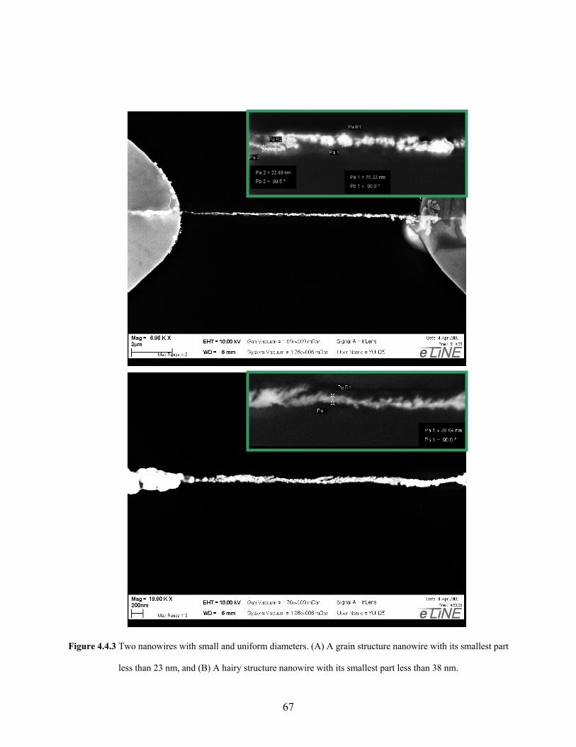
Figure 4.4.3 Two nanowires with small and uniform diameters. (A) A grain structure nanowire with its smallest part
less than 23 nm, and (B) A hairy structure nanowire with its smallest part less than 38 nm.
67

Diameter vs. Voltage
0
20
40
60
80
100
120
50nA (6.5µm) 30nA (3.5µm) 30nA (4µm) 10nA (3.5µm) 10nA (4µm)
Growth current (Channel Length)
Nan
owire
Dia
met
er (n
m)
V=0 V= -10V
(A)
Growth Time vs Voltage
0
10
20
30
40
50
60
50nA (6.5µm) 30nA (3.5µm) 30nA (4µm) 10nA (3.5µm) 10nA (4µm)
Growth current (Channel length)
Gro
wth
tim
e (s
)
V=0 V= -10V
(B)
Figure 4.4.4 (A) The change of diameters from Vg= 0 to Vg= −10V under different conditions. (B) The change of
growth time from Vg= 0 to Vg= −10 V under different growth conditions.
68

Experimental data prove the effects of the gate electric field. As shown in Figures 4.4.3 A
and B, two nanowires with tiny diameters are fabricated using the gate-assisted growth method.
Figure 4.4.3 is a grain structure nanowire, while Figure 4.4.3 B is a hairy structure nanowire. As
shown in the images, the nanowires are quite uniform along a great distance, but the diameters
are as small as 20 nm to 30 nm.
In order to further demonstrate the gate effect, a set of comparison experiments were
done. Figures 4.4.4 A and B present the experimental data on diameter and growth time,
respectively. Nanowires were grown under different growth conditions, such as growth current
and nanochannel length with Vg = 0 or Vg= −10V. The growth currents had three different values:
50 nA, 30 nA, and 10 nA. There were three different kinds of channel length: 6.5µm, 4µm and
3.5µm length. Channel width remained the same at 100 nm in these three different kinds of
channels. Figure 4.4.3 A shows that the nanowires grown with a gate electric field had smaller
widths in all five different conditions. It is obvious that the usage of the gate electric field
assisted the growth of the nanowire within the channels and shrinking the nanowire diameters.
This idea can also be proved by the growth time change from Vg = 0 to Vg= −10V. Figure 4.4.3
B illustrates that the growth time with gate voltage is much smaller than that without gate voltage
in five conditions - more than 50% in some cases. The decreased growth time results in a higher
growth efficency and a higher throughput of nanowire fabrication. According to the relationship
[14, 38]:
( )nFL
VtItr mdepdep
π2
= (4.1)
where r(t) is the diameter of the nanowire, Idep represents the growth current, tdep represents the
growth time, Vm is the molar volume of the deposited material, n is the number of electrons
69
transferred from the ion during deposition, and L is the total length of the channel. It is clear that
diameter . This relationship shows that the two charts are in accordance with each other. 2/1tr ∝
Therefore, this gate-assisted nanowire growth is theoretically sound and, as proven in our
preliminary experiments, this finding is very promising in controlling the nanowire growth and
in obtaining thinner nanowire with higher fabrication efficiency. Furthermore, gate-assisted
growth opens an entirely new idea of applying multiple electric fields from different directions
during electrophoresis deposition.
70

5.0 CONCLUSION AND FUTURE WORK
5.1 CONCLUSION In this work, we presented an effective way of fabricating palladium (Pd) metallic nanowires
with less than a 100 nm diameter using electrophoresis deposition. PMMA nanochannels with
100nm width and 3.5 µm to 6.5 µm length were fabricated using e-beam lithography on the
surface of a template. By applying a constant DC current through two gold electrodes, Pd single
nanowires were electro-deposited inside these PMMA channel. AFM and SEM were used to
characterize the surface properties of the single nanowires, while a semiconductor analyzer was
used to test their resistance. SEM images showed that the nanowires grown were thin and
straight, while AFM images showed that the nanochannels made by EBL were clean and uniform
and the nanowires were vertically uniform with a height of around 100 nm.
Hydrogen sensors based on these Pd single nanowires were successfully integrated by
wirebonding nanowires to wafer holders and then applying an external circuit, including a
current amplifier, a data acquisition system, and a control system based on Labview. A gas
sensing system based on a mass flow controller was set up; a hydrogen gas concentration from
10% to 2 ppm could be attained with proper control. The best tested hydrogen concentration
yielded by our devices is 5 ppm, which is the optimum value we found in the literature for pure
Pd hydrogen sensors. This result not only demonstrated the capability of Pd related
71

nanostructures in hydrogen detection, but more importantly, it also showed the advantage of a
single nanowire structure in the sensor area.
Nanowire growth and sensing mechanisms were also studied in depth in this work. Three
different nanowire structures were found, including plain, grain, and hairy structures. The growth
mechanisms were discussed, and the growth control of nanowire structure was attempted by
varying growth currents. In addition, two separate sensing signals were discovered when
different nanowires were used in hydrogen detection. This phenomenon was not seen in other
similar research. These experimental results suggest the need for a complete discussion on
proposed different sensing mechanisms regarding three different nanowire structures.
This work also proposed and proved a novel idea of electrophoresis deposition. Rather
than applying one direction electric field during growth, another extra electric field was applied
inside the channel from the back gate by connecting the silicon substrate to a reverse biased
voltage. This configuration helps pull down positive charged Pd2+ ions and the experimental
results proved gate voltage’s impact on nanowire diameter and growth time. Nanowires with tiny
diameters and uniform structures were fabricated with a higher efficiency using this new gate-
assisted growth. This idea opens a brand new vision of applying multiple electric fields during
electrophoresis deposition that forms a 2D or even 3D electric field to achieve easier growth
control.
72
5.2 LIST OF RESULTING PUBLICATION
[1] - Single Palladium Nanowire Via Electrophoresis Deposition Used as Ultra Sensitive
Hydrogen Sensor, Yushi Hu (Department of Electrical and Computer Engineering, University of
Pittsburgh, Pittsburgh, PA, USA), David Perello, Usman Mushtaq, and Minhee Yun. (Submitted)
5.3 FUTURE WORK
This work successfully demonstrated the growth of 50 nm to 100 nm diameter Pd single
nanowires. Hydrogen sensors based on these nanowires were fabricated and used in detection; a
fairy good sensitivity was achieved. However, this work mainly focused on the fabrication of
metallic (Pd) nanowires and hydrogen detection. Also, with the diameter of nanowires
approximately 100 nm, it was difficult to get down to less than 50 nm. Thus, developments of
this project could go two possible ways: (1) other sensors based on different materials
(biosensors based on conducting polymers), and (2) production of thinner nanowire.
Biosensor is becoming a more and more important device not only in biological and
medical areas but also in environmental and social security areas [49]. Biosensor refers to a
device that could detect a certain analyte and generate traceable electrical or optical signals. The
applications of biosensors, such as detection of glucose for diabetes patients and detection of
viruses in blood, have made them essential devices in hospitals and health related organizations.
Biosensors are also becoming regular gadgets used by housewives to detect drug residual in
foods or toxic substances in water. The remote detection of airborne bacterial makes them an
73

effective tool in the area of social security. In all, biosensor is emerging as a commonly used tool
in a profitable market.
Biosensors based on nanowires have been proposed long ago by many research groups.
Nanowire devices are suitable in this area because of their small size, high sensitivity, and low
power consumption. Configured with the proper active elements on the surface of the nanowire,
the existence of a certain analyte (i.e. glucose and DNA) would bind with the active elements
and result in a change of the nanowire, such as conductance. This change is detectable and forms
the basis of a sensor.
As a very promising candidate, conducting polymer, such as poly-pyrrole (PPy) and poly-aniline
(PANI), has been extensively researched in integrating biosensors because of its special
electrical and optical properties [50]. PPy and PANI nanowires fabricated using electrophoresis
deposition have also been reported [51]. Given the reliability of a single nanowire growth
method described in this work, single nanowire based on PPy and PANI can be synthesized with
a small diameter as well as good surface properties by applying the gate-assisted growing
mechanism.
An important advantage of nanowire based biosensors is their fast response and high
sensitivity. As the change of signals is generated by the change of the properties of the nanowire
itself, such as conductance, the one dimensional nanowire is easily affected by external change.
The binding of an external charge could easily cause carrier depletion or accumulation in the
nanowire; this process occurs quickly because of the nanowire’s small diameter.
Another possible advantage of our nanowire sensor is the feasibility of Field Effect
Transistor (FET) structure. As mentioned in part 4.4, a back-gate structure could be used to apply
74

another electric field to the channel. With a grown nanowire, the back gate forms an actual FET
structure. Thus, a pre-aligned FET nanowire sensor device is easily obtained using our method;
the sensitivity of this device could be optimized by tuning the gate voltage carefully.
The second route of developing this work involves thinner nanowires which can be made
with the help of gate-assisted growth and the production of narrower PMMA channels. As
proved in part 4.4, gate-assisted growth has a very obvious effect in limiting the diameter of
nanowire; it simultaneously helps grow thinner and more uniform nanowires. On the other hand,
PMMA channels can be made smaller to further restrict the growth of Pd nanowires during
electrophoresis deposition. With a proper combination of EBL parameters and PMMA thickness,
nanochannels with diameters less than 40 nm are obtainable [42]. In this case, the growth of
nanowire could be further restricted by the channel; its diameter could be kept around 40 nm.
The decrease of the nanowire diameter not only facilitates the study of the basic properties of
nanowires, such as the relationship between nanowire diameters and the growth of thin nanowire
using electrophoresis deposition, but it also elevates the sensitivity of nanowire sensors to
another level because of the nanowire’s reduced lateral size as well as increased surface to
volume ratio.
75
APPENDIX
CONDUCTANCE OF SINGLE METALLIC NANOWIRE
As mentioned in part 2.2.1, the conductance of the nanowire can be expressed by Landauer’s
formula in (2.6). The T or transmission function in the formula is calculated using Green’s
functions of the central region and couplings to the leads [21]:
(A.1)
where is the transmission coefficient, and are the retarded (r) and advanced (a) Green’s
functions of the center (c), and , are functions for couplings to the leads (left and right). The
central region, which is the computationally important part, may include tube junctions, defects,
or vacancies. Therefore, any change in the atomic structure or the radius can induce changes
among C, L, and R locations and alter the level spacing and the occupancy probability of the
states. This, in turn, leads to detectable changes in conductance.
Electrical conduction in nanowires can be approximated as a ballistic scattering of
electrons along the one-dimensional quasi-periodic super lattice of finite length [25]. Under this
condition, the conductance of a specific nanowire should be decided by the number of states
occupied by electrons existing in the nanowire while each electron state would contribute a
conductance of G, which is expressed by Landuaer’s equation in (2.6). Assuming that the
76

quantum states of the electrons in a nanowire correspond to the eigenstates of Schrödinger
Equation:
, , , , (A.2)
then we should be able to express the transmission coefficient as:
∑ (A.3)
where T represents the total transmission coefficient, n represents a specific quantum state
number and Tn represents the transmission coefficient of the state n. By combining equation (2.6)
and equation (A.3), we can find out the expression for nanowire conductance as [25]:
2 / ∑ (A.4)
Given a certain Fermi energy level EF, since only the energy states En that are below EF can be
occupied by electrons while the states above EF are empty, the states that contribute to
conductance would be those below EF. Based on this idea, the transmission coefficient of a
certain state n can be expressed as:
0,1, (A.5)
In this equation, we assume that the transmission coefficient equals 1 since in all cases it is very
close to 1 [25]. By combini e ducta ce anowire as: ng (A.4) and (A.5), we can express th con n of n
2 / ∑ 1 2 / , (A.6)
77

It is clear from (A.6) that the nanowire conductance is directly related to the total number of
states (N+1) that is lower than the Fermi level. In other words, the conductance is decided by
how many energy states are occupied by electrons.
As indicated by the above concept, conductance of the nanowire would decrease when
the diameter of nanowire decreases, since fewer atoms in the cross section indicates less electron
states that can contribute to the conductance. It is also predicted that as the diameter approaches
the atom size, the conductance will change step by step instead of continuously. Multiple
researchers have found these phenomena, and Figure A.1 illustrates a typical quantum
conductance phenomenon in a global histogram from Ag nanowires [26].
In order to discuss how the conductance of nanowire changes with the diameter in detail, we can
assume that the Fermi Level EF in the nanowire stays constant as the diameter changes. We can
then focus on how the energy of eigenstates changes using the Schrödinger Equation (A.2). It is
obvious that we need to set a proper boundary condition to work out the energy of eigenstates. If
we assume that the electron can only exist inside the nanowire structure and that the nanowire is
a perfect cylinder structure with radius a and length L (as illustrated in Figure A.2), we can build
the following equations [27]:
, , , ,
, 0 (A.7)
If we assume that the nanowire structure is perfect in the z direction, given that the length of the
nanowire is much larger than the radius (L>>a), we can transfer this problem into a cylindrical
box. Note: Here we ignored the periodic atomic fields existing in the nanowire but assumed the
space inside the nanowire to be a free space in order to simplify the situation and get a rough
idea on how the energy states change with the diameter. In this case, the eigen energies to the
78

Figure A.1 Quantum conductance found in silver nanowires. Reprinted with permission from [26]. Copyright
(2008) by the American Physical Society.
79

L
Y
Z a
X
Figure A.2 Illustration of an ideal nanowire structure
80

cylindrical box c uld bo e expressed as [27]:
2 / / / , 0, (A.8)
where n, l, nz are the eigen numbers in x, y, z directions, a is the radius of the nanowire, and L is
the length. Jn(x) is the Bessel function, and xnl corresponds to the values that make this function
zero. A few first zeros of the Bessel functions are listed in Table 1 [27]:
Let’s consider the eigen energies given by (A.8). In the nanowire, it is assumed that L>>a.
Therefore the second term n the d and (2.14) becomes: o right side of the equation can be ignore
/2 / , 0 (A.9)
For a specific eigen state, such as n=1 and l=2, the value of xnl is set. A direct relationship
between eigen energy Enlnz and radius a can be found as:
1/ (A.10)
It is clear from (A.10) that as the radius of the nanowire is decreased, the energy of a certain
eigenstate Eabc will be increased. From (A.6) the conductance of the nanowire is decided by the
total number of eigenstates below EF, and the number N means the Nth state which has the
maximum energy under the Fermi Level. If radius a is decreased, EN will be increased and lifted
above the Fermi Level; no electron can occupy this state any more. As a result, the total number
of the states below Fermi Level is decreased, thereby decreasing the conductance. Consequently,
the decrease of conductance of the nanowire is directly related to the radius of the nanowire.
The conductance of nanowires is no longer decided by a classical relationship (2.5)
because of the quantum transportation of electrons. A discussion between the conductance and
nanowire radius based on Landauer’s Formalism and ideal assumptions shows that the
conductance is directly related to the radius and that the conductance decreases when the radius
decreases.
81
Table 3 First few xnl values to make Bessel function zero
1=l 2=l 3=l
lx0 2.40 5.52 8.65
lx1 3.83 7.02 10.17
lx2 5.14 8.42 11.62
lx3 6.30 9.76 13.02
82

BIBLIOGRAPHY
[1]. Noboru Yamazoe, Toward innovations of gas sensor technology, Sensors and Actuators B 108 (2005) 2–14.
[2]. X. Bevenot, A. Trouillet, C. Veillas, H. Gagnaire, and M. Clement, Hydrogen leak detection using an optical fibre sensor for aerospace applications, Sensors and Actuators B 67 (2000) 57–67.
[3]. Hiroyasu Iwaharaa, Yamato Asakurab, Koji Katahirac, and Masahiro Tanaka, Prospect of hydrogen technology using proton-conducting ceramics, Solid State Ionics 168 (2004) 299–310
[4]. Magdalena Momirlana, and T.N.Veziroglub, The properties of hydrogen as fuel tomorrowin sustainable energy system for a cleaner planet, International Journal of Hydrogen Energy 30 (2005) 795 – 802
[5]. Constantinos Christofides and Andreas Mandelis, Solid-state sensors for trace hydrogen gas detection, J. Apply. Phys. 68 (6), 1990 R1.
[6]. Wei Lu and Charles M. Lieber, Nanoelectronics from the bottom up, Nature Materials 6 (2007) 841-850
[7]. Wei Lu and Charles M. Lieber, Semiconductor Nanowires, J. Phys. D: Appl. Phys. 39 (2006) R387-R406
[8]. Jiming Bao, Mariano A. Zimmler, Federico Capasso, Xiaowei Wang and Z. F. Ren, Broadband ZnO Single-Nanowire Light-Emitting Diode, Nano Lett., Vol. 6, No. 8, (2006) 1719-1722
[9]. Adam K. Wanekaya, Wilfred Chen, Nosang V. Myung, and Ashok Mulchandani, Nanowire-Based Electrochemical Biosensors, Electroanalysis 18, 2006, No. 6, 533 – 550
[10]. Zhiyong Fan and Jia G. Lua, Gate-refreshable nanowire chemical sensors, Appl. Phys. Lett. 86, 123510 (2005)
[11]. M. E. Bourg, W. E. van der Veer, A. G. Gruell, and R. M. Penner, Electrodeposited Submicron Thermocouples with Microsecond Response Times, Nano Lett., Vol. 7, No. 10, (2007) 3208-3213
83

[12]. Siegmar Roth and David Carroll, One-Dimensional Metals, WILEY-VCH Publishing, Weinheim, Germany, 2004
[13]. Fernando Patolsky and Charles M. Lieber, Nanowire nanosensors, Materialstoday, Apr. (2005) 20-27
[14]. Frederic Favier, Erich C. Walter, Michael P. Zach, Thorsten Benter, and Reginald M. Penner, Hydrogen Sensors and Switches from Electrodeposited Palladium Mesowire Arrays, Science Vol. 293 21 (2001) 2227-2231
[15]. Kyun Tae Kim, Sang Jun Sim, and Sung Min Cho, Hydrogen Gas Sensor Using Pd Nanowires Electro-Deposited Into Anodized Alumina Template, IEEE Sensors Journal, Vol. 6, No. 3, (2006) 509-513
[16]. Pai-Chun Chang, Zhiyong Fan, Dawei Wang, Wei-Yu Tseng, Wen-An Chiou, Juan Hong, and Jia G. Lu, ZnO Nanowires Synthesized by Vapor Trapping CVD Method, Chem. Mater. 2004, 16, 5133-5137
[17]. Minhee Yun, Nosang V. Myung, Richard P. Vasquez, Choonsup Lee, Erik Menke, and Reginald M. Penner, Electrochemically Grown Wires for Individually Addressable Sensor Arrays, Nano Lett., Vol. 4, No. 3, (2004) 419-422
[18]. S. Kagoshima, H. Nagasawa and T. Sambongi, One-Dimensional Conductors, Shokabo Publishing Co., Ltd., Tokyo 1982, Springer-Verlag Berlin Heidelberg New York
[19]. Andrew B. Greytak, Lincoln J. Lauhon, Mark S. Gudiksen, and Charles M. Lieber, Growth and transport properties of complementary germanium nanowire field-effect transistors, Appl. Phys. Lett., Vol. 84, No. 21, (2004) 4176-4178
[20]. Gregory S Snider and R Stanley Williams, Nano/CMOS architectures using a field-programmable nanowire interconnect, Nanotechnology 18 (2007) 035204
[21]. S. Ciraci, ABuldum, and Inder P Batra, Quantum effects in electrical and thermal transport through nanowire, J. Phys.: Condens. Matter 13 (2001) R537-R568
[22]. Xiangfeng Duan, Yu Huang, Ritesh Agarwal, and Charles M. Lieber, Single-nanowire electrically driven lasers, Nature 421, 241-245 (2003)
[23]. C. A. Stafford, Metal Nanowires: Quantum Transport, Cohesion, and Stability, Phys. Stat. Sol. (b) 230, No. 2, (2002) 481–489
[24]. S. Michotte, S. Matefi-Tempfli, and L. Piraux, 1D-transport properties of single superconducting lead nanowires, Physica C 391 (2003) 369–375
[25]. Y. Arakawa, K. Furuya, S. Komiyama, and H. Nakashima, Mesoscopic Physics and Electronics, Berlin; Heidelberg; New York; Barcelona; Budapest; Hong Kong; Milan; Paris; Santa Clara; Singapore; Tokyo: Springer, (1998)
84

[26]. V. Rodrigues, J. Bettini, A. R. Rocha, L. G. C. Rego, and D. Ugarte, Quantum conductance in silver nanowires: Correlation between atomic structure and transport properties, Physical Review B, Vol. 65, 153402 (2002)
[27]. Richard L. Liboff, Introductory Quantum Mechanics, 4th edition, Addison Wesley, 2003
[28]. Igor Aharonovich, Shoshana Tamir, and Yeshayahu Lifshitz, Growth of SiOx nanowires by laser ablation, Nanotechnology 19 (2008) 065608
[29]. X.M. Cai , A.B. Djurišić, M.H. Xie, GaN nanowires: CVD synthesis and properties, Thin Solid Films 515 (2006) 984–989
[30]. Shi-biao Xiang, and Xu Xiang, Novel 2D self-assembled arrays of SiOx nanowire bundles, Materials Letters 61 (2007) 3662–3665
[31]. Yukihito Kondo, and Kunio Takayanagi, Gold Nanobridge Stabilized by Surface Structure, Phys. Rev. Lett., Vol. 79, No. 18, (1997) 3455-3458
[32]. Yukihito Kondo, and Kunio Takayanagi, Synthesis and Characterization of Helical Multi-Shell Gold Nanowires, Science, Vol. 289 No. 28 (2000) 606-608
[33]. Pablo Z. Coura, Sergio B. Legoas, Anderson S. Moreira, Fernando Sato, Varlei Rodrigues, Socrates O. Dantas, Daniel Ugarte, and Douglas S. Galvao, On the Structural and Stability features of Linear Atomic Suspended Chains Formed from Gold Nanowires Stretching, Nano Lett., Vol. 4, No. 7, (2004) 1187-1191
[34]. Yanfa Yan, Ping Liu, M. J. Romero, and M. M. Al-Jassim, Formation of metallic zinc nanowires, J. Appl. Phys., Vol. 93, No. 8, (2003) 4807-4809
[35]. Dmitri Routkevitch, Terry Bigioni, Martin Moskovits, and Jing Ming Xu, Electrochemical Fabrication of CdS Nanowire Arrays in Porous Anodic Aluminum Oxide Templates, J. Phys. Chem. (1996) 100, 14037-14047
[36]. A. J. Yin, J. Li, W. Jian, A. J. Bennett, and J. M. Xu, Fabrication of highly ordered metallic nanowire arrays by electrodeposition, Appl. Phys. Lett., Vol. 79, No. 7, (2001) 1039-1041
[37]. Massood Z. Atashbar, Deep Banerji, and Srikanth Singamaneni, Room-Temperature Hydrogen Sensor Based on Palladium Nanowires, IEEE Sensors Journal, Vol. 5, No. 5, (2005) 792-797
[38]. Erich C. Walter, Michael P. Zach, Fredric Favier, Benjamin J. Murray, Koji Inazu, John C. Hemminger, and Reginald M. Penner, Metal Nanowire Arrays by Electrodeposition, ChemPhysChem. (2003) 4, 131 – 138
[39]. E. J. Menke, M. A. Thompson, C. Xiang, L. C. Yang, and R. M. Penner, Lithographically patterned nanowire electrodeposition, Nature Materials, Vol. 5, (2006) 914-919
85

86
[40]. Milan Paunovic and Mordechay Schlesinger, Fudanmentals of Electrochemical Deposition, John Wiley & Sons, Inc., 1998.
[41]. NANOTM PMMA & Copolymer, Microchem Website, http://www.microchem.com/products/pdf/PMMA_Data_Sheet.pdf
[42]. Michael Kohler, and Wolfgang Fritzsche, Nanotechnology, WILEY-VCH Publishing, Weinheim, Germany, 2004
[43]. Andreas Mandelis and Jose A. Garcia, Pd/PVDF thin film hydrogen sensor based on laser-amplitude-modulated optical-transmittance: dependence on H2 concentration and device physics, Sensors and Actuators B 49 (1998) 258–267
[44]. Ted B. Flanagan and W. A. Oates, The Palladium-Hydrogen System, Annu. Rev. Mater. Sci. (1991) 21: 269-304
[45]. F. A. Lewis, The Palladium Hydrogen System, Academic Press, NY (1967).
[46]. J. C. Barton, F. A. Lewis, and (in part) Miss I. Woodward, Hysteresis of the Relationships between Electrical Resistance and the Hydrogen Content of Palladium, Trans. Faraday Soc. 59 (1963), p. 1201. DOI: 10.1039/TF9635901201
[47]. Yeonho Im, Choonsup Lee, Richard P. Vasquez, Mangesh A. Bangar, Nosang V. Myung, Eric J. Menke, Reginald M. Penner, and Minhee Yun, Investigation of a Single Pd Nanowire for Use as a Hydrogen Sensor, Small (2006) 2, No. 3, 356–358
[48]. T. A. Witten and L. M. Sander, Diffusion-limited Aggregation, Phys. Rev. B, Vol. 27, No. 9, (1983) 5686-5697
[49]. Fernando Patolsky, Brian P. Timko, Gengfeng Zheng, and Charles M. Lieber, Nanowire-Based Nanoelectronic Devices in the Life Sciences, MRS Bulletin, Vol. 32, (2007) 142-149
[50]. Manju Gerard, Asha Chaubey, and B.D. Malhotra, Application of conducting polymers to biosensors, Biosensors & Bioelectronics 17 (2002) 345–359
[51]. Kumaran Ramanathan, Mangesh A. Bangar, Minhee Yun, Wilfred Chen, Ashok Mulchandani, and Nosang V. Myung, Individually Addressable Conducting Polymer Nanowires Array, Nano Lett., Vol. 4, No. 7, (2004) 1237-1239
[52]. Yeonho Imb, Richard P. Vasquezc, Choonsup Leec, Nosang Myungd, Reginald Pennere, and Minhee Yun, Single metal and conducting polymer nanowire sensors for chemical and DNA detections, Journal of Physics: Conference Series 38 (2006) 61–64


![Palladium-Catalyzed Benzo[d]isoxazole Synthesis by … · Palladium-Catalyzed Benzo[d]isoxazole Synthesis by C-H Activation/[4+1]Annulation . Pingping Duan, a. Yunfang Yang, a. Xinhao](https://static.fdocuments.net/doc/165x107/5aff0df97f8b9a994d8fda4e/palladium-catalyzed-benzodisoxazole-synthesis-by-benzodisoxazole-synthesis.jpg)


