
Single-Event Transient Pulse-Width Measurements … Engineering 6/10/09 Gadlage - MURI Review 1...
23
Vanderbilt Engineering 6/10/09 Gadlage - MURI Review 1 Single-Event Transient Pulse-Width Measurements in Advanced Technologies Matthew Gadlage MURI Review June 10, 2009
Transcript of Single-Event Transient Pulse-Width Measurements … Engineering 6/10/09 Gadlage - MURI Review 1...

Vanderbilt Engineering
6/10/09 Gadlage - MURI Review 1
Single-Event Transient Pulse-Width Measurements in Advanced Technologies
Matthew Gadlage
MURI Review June 10, 2009

Vanderbilt Engineering
6/10/09 Gadlage - MURI Review 2
Outline
Background What is a single event transient (SET)? Description of the SET Measurement Circuit Previous Results from 130 and 90 nm Bulk Processes
SET Measurements in a 180-nm FDSOI Process – Experimental Results – TCAD Simulations
Effect of Temperature on SET Pulse Widths Cold Temperature (130-nm bulk) Elevated Temperature (90-nm bulk, 130-nm bulk, & 180-nm SOI)
– Comparison between Bulk and SOI Work in Progress
New SET Chip Designs Summary

Vanderbilt Engineering
6/10/09 Gadlage - MURI Review 3
Outline
Background What is a single event transient (SET)? Description of the SET Measurement Circuit Previous Results from 130 and 90 nm Bulk Processes
SET Measurements in a 180-nm FDSOI Process – Experimental Results – TCAD Simulations
Effect of Temperature on SET Pulse Widths Cold Temperature (130-nm bulk) Elevated Temperature (90-nm bulk, 130-nm bulk, & 180-nm SOI)
– Comparison between Bulk and SOI Work in Progress
New SET Chip Designs Summary

Vanderbilt Engineering
6/10/09 Gadlage - MURI Review 4
Single Event Transients
• Combinational logic soft errors are a major reliability issue for advanced CMOS processes
• Knowing the digital single event transient (SET) pulse widths are key to determining error rates
Gadlage et al., TNS 2007 Image taken from Mavis et al., IRPS 2002
1.0 V
1.2 V
1.5 V
2.0 V

Vanderbilt Engineering
6/10/09 Gadlage - MURI Review 5
SET Measurement Circuit
Circuit measures SET pulse width in units of stage delay Delay changes with technology (~20 ps for 65-nm, ~100 ps for 130-nm)
Target circuit can consist of almost any combinational logic chain (inverters, NANDs, NORs, etc.)
Structure has been successfully implemented in 130-nm bulk, 90-nm bulk, 180-nm FDSOI, and 150-nm FDSOI
Narasimham et al. TDMR 2006
Vanderbilt Engineering
6/10/09 Gadlage - MURI Review 6
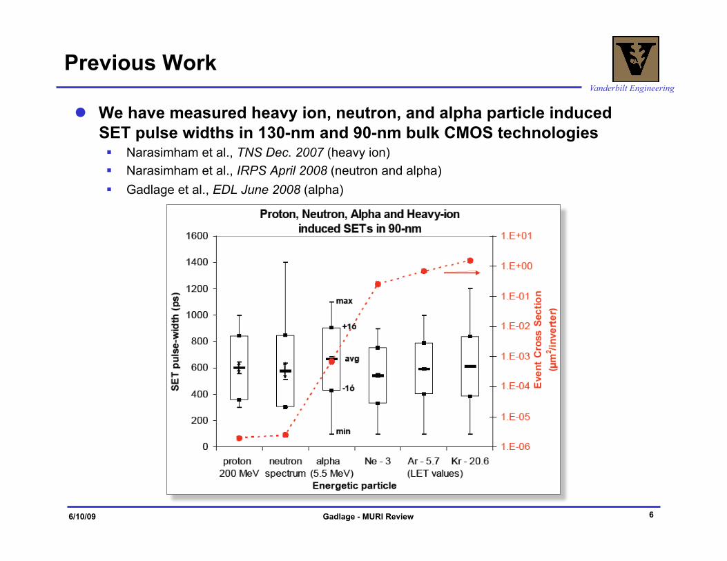
Previous Work
We have measured heavy ion, neutron, and alpha particle induced SET pulse widths in 130-nm and 90-nm bulk CMOS technologies Narasimham et al., TNS Dec. 2007 (heavy ion) Narasimham et al., IRPS April 2008 (neutron and alpha) Gadlage et al., EDL June 2008 (alpha)
Vanderbilt Engineering
6/10/09 Gadlage - MURI Review 7
Outline
Background What is a single event transient (SET)? Description of the SET Measurement Circuit Previous Results from 130 and 90 nm Bulk Processes
SET Measurements in a 180-nm FDSOI Process – Experimental Results – TCAD Simulations
Effect of Temperature on SET Pulse Widths Cold Temperature (130-nm bulk) Elevated Temperature (90-nm bulk, 130-nm bulk, & 180-nm SOI)
– Comparison between Bulk and SOI Work in Progress
New SET Chip Designs Summary

Vanderbilt Engineering
6/10/09 Gadlage - MURI Review 8
SET Measurements in 180-nm FDSOI
MIT Lincoln Lab has built the SET measurement circuit on their 180-nm fully depleted SOI technology
Consists of two target circuits with 200 inverters each
• One with body ties
• One without body ties
Smallest measurable SET is 70 ps
Laser data were presented last year at NSREC (Gouker et al., TNS Dec. 2008)
Laser testing results from Gouker et al. showing how SET pulses broaden as they propagate through an
inverter chain in this fully depleted SOI technology.

Vanderbilt Engineering
6/10/09 Gadlage - MURI Review 9
180-nm FDSOI SET Pulse Width Measurements
SET Pulse Width Distribution for an LET of 69 MeV-cm2/mg
Heavy ion data obtained at Berkeley National Labs
Cross section and measured pulse widths are significantly shorter for the body contacted inverters.
Pulse broadening effects are greatly reduced with the body contact.
For the circuit with body ties, the average SET pulse width increases with LET.

Vanderbilt Engineering
6/10/09 Gadlage - MURI Review 10
Extracting Pulse Widths from the Floating Body Circuit
A linear convolution of the known broadening rate (~4 ps/inverter) and the measured SET pulse width distribution was performed. The original (i.e. non-broadened) SET distribution can then be obtained for the floating body circuit.
A similar analysis can be performed on any SET measurement circuit where pulse
broadening may be an issue.
SET Pulse Width Distribution Analysis for an LET of 69 MeV-cm2/mg

Vanderbilt Engineering
6/10/09 Gadlage - MURI Review 11
180-nm FDSOI TCAD Results
MIT Lincoln Lab has provided all the information needed to perform TCAD & mixed-mode simulations.
Both the NMOS and PMOS devices have been calibrated to the transistor sizes used in our SET pulse width measuring circuit.
Performed numerous simulations to help explain the heavy ion results.
Simulations showing that the presence of a body contact does not significantly change the generated SET pulse width.
Simulations illustrating the dependence of ion strike location on the SET pulse width.
TCAD Model

Vanderbilt Engineering
6/10/09 Gadlage - MURI Review 12
Outline
Background What is a single event transient (SET)? Description of the SET Measurement Circuit Previous Results from 130 and 90 nm Bulk Processes
SET Measurements in a 180-nm FDSOI Process – Experimental Results – TCAD Simulations
Effect of Temperature on SET Pulse Widths Cold Temperature (130-nm bulk) Elevated Temperature (90-nm bulk, 130-nm bulk, & 180-nm SOI)
– Comparison between Bulk and SOI Work in Progress
New SET Chip Designs Summary

Vanderbilt Engineering
6/10/09 Gadlage - MURI Review 13
Cold Temperature Experiment (130-nm Bulk)
• Testing was performed with Xenon ions at Texas A&M with an LET (Linear Energy Transfer) of 40 MeV-cm2/mg on the 130-nm bulk circuit.
• The temperature of the IC was controlled using a Dewar designed (in collaboration with Georgia Tech) specifically for cold temperature radiation testing.
• Ion exposures were carried out at temperatures from -140o C to 20o C.
Ramachandran et al., IPPW 2008

Vanderbilt Engineering
6/10/09 Gadlage - MURI Review 14
Cold Temperature Experimental Results
• SET pulse widths are measured in this circuit in units of a latch delay which changes with temperature.
• The heavy ion results show that the SET measurements in units of latches did not change with temperature.

Vanderbilt Engineering
6/10/09 Gadlage - MURI Review 15
Cold Temperature Experimental Results
130-nm Bulk Cold Temperature Results
~250 SET events were measured at each
temperature

Vanderbilt Engineering
6/10/09 Gadlage - MURI Review 16
Elevated Temperature Experiment (Bulk and SOI)
Picture of the setup at TAMU
• Testing was performed with Xenon ions at Texas A&M with an LET of 52 MeV-cm2/mg on the 90-nm bulk, 130-nm bulk, and 180-nm SOI circuits.
• The temperature of the IC was controlled through a resistive heater (attached to the package) and monitored by a resistive sensor.
• The floating body SOI circuit was also tested using a laser at NRL.

Vanderbilt Engineering
6/10/09 Gadlage - MURI Review 17
Elevated Temperature Experimental Results
Temp. Average SET
Max. SET
25˚ C 920 ps 1500 ps 50˚ C 970 ps 1600 ps
100˚ C >1260 ps >1900 ps
Temp. Average SET
Max. SET
25˚ C 670 ps 980 ps 50˚ C 620 ps 980 ps
100˚ C 620 ps 1050 ps
Temp. Average SET
Max. SET
25˚ C 520 ps 1030 ps 50˚ C 611 ps 1199 ps
100˚ C 633 ps 1320 ps 130-nm Bulk Heavy Ion
(~100 SET events recorded at each temperature)
90-nm Bulk Heavy Ion (~350 SET events recorded at each temperature)
Both bulk processes show an increase in SET pulse width
with temperature. 180-nm SOI Laser (~10000 laser events recorded at each position/temperature)
180-nm SOI Heavy Ion (~100 SET events recorded at each temperature)

Vanderbilt Engineering
6/10/09 Gadlage - MURI Review 18
90-nm Bulk TCAD sims
Show a pulse width increase with temperature
180-nm FDSOI TCAD sims
Show a slight pulse width decrease with temperature
TCAD Temperature Simulations
Increasing Temperature Increasing Temperature
… …
Vanderbilt Engineering
6/10/09 Gadlage - MURI Review 19
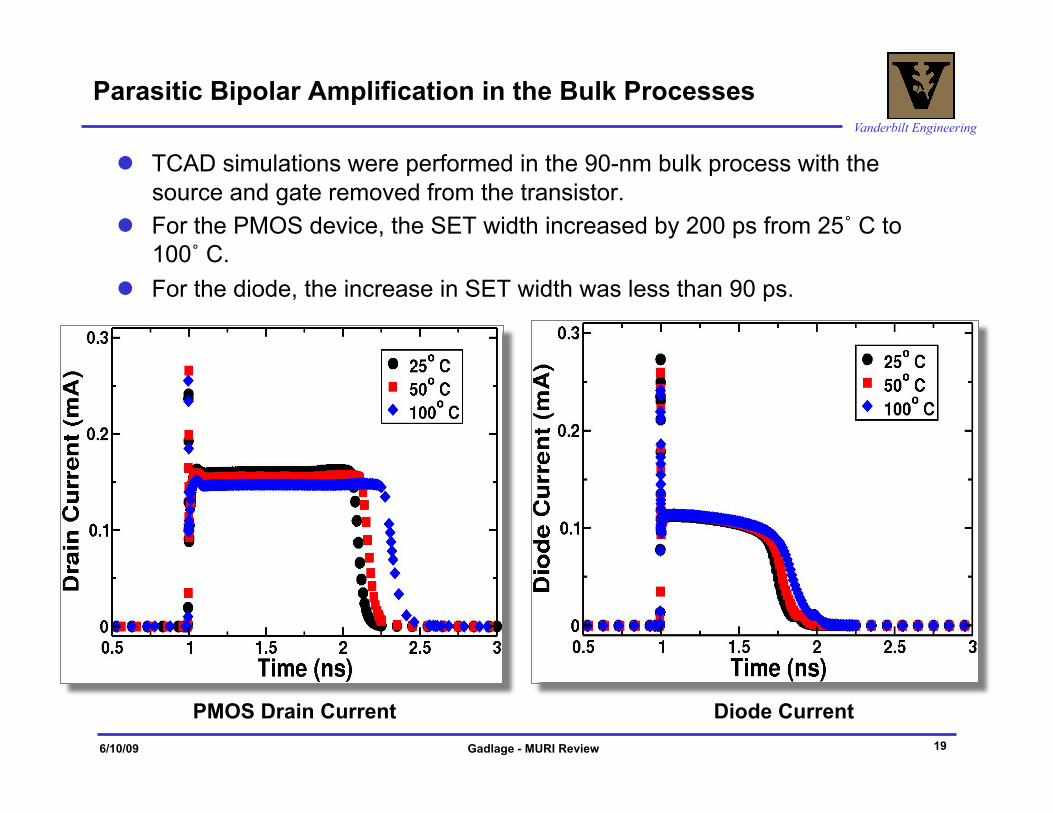
Parasitic Bipolar Amplification in the Bulk Processes
PMOS Drain Current Diode Current
TCAD simulations were performed in the 90-nm bulk process with the source and gate removed from the transistor.
For the PMOS device, the SET width increased by 200 ps from 25˚ C to 100˚ C.
For the diode, the increase in SET width was less than 90 ps.

Vanderbilt Engineering
6/10/09 Gadlage - MURI Review 20
Outline
Background What is a single event transient (SET)? Description of the SET Measurement Circuit Previous Results from 130 and 90 nm Bulk Processes
SET Measurements in a 180-nm FDSOI Process – Experimental Results – TCAD Simulations
Effect of Temperature on SET Pulse Widths Cold Temperature (130-nm bulk) Elevated Temperature (90-nm bulk, 130-nm bulk, & 180-nm SOI)
– Comparison between Bulk and SOI Work in Progress
New SET Chip Designs Summary

Vanderbilt Engineering
6/10/09 Gadlage - MURI Review 21
SET Test Chip Designs Currently in Fab
TI 45-nm 12 stage measurement circuit, ~90 ps per stage Target circuit = 1000 inverter chain
150-nm 3D FDSOI Two SET measurement circuits on each of three layers
– One circuit with body ties and one without – Target circuit consists of eight, 200 inverter chains OR’ed together.
Also included target circuit designs to differentiate between SETs originating from either NMOS or PMOS strikes
65-nm CMOS10SF Included 5 different target circuits
– 1000 inverter chain w/ PMOS devices in separate wells – Inverter chain w/ PMOS devices in the same well – Small inverter chains OR’ed together – N-Hit circuit – P-Hit circuit

Vanderbilt Engineering
6/10/09 Gadlage - MURI Review 22
SET Test Chip Designs Currently in Fab
TI 45-nm 12 stage measurement circuit, ~90 ps per stage Target circuit = 1000 inverter chain
150-nm 3D FDSOI Two SET measurement circuits on each of three layers
– One circuit with body ties and one without – Target circuit consists of eight, 200 inverter chains OR’ed together.
Also included target circuit designs to differentiate between SETs originating from either NMOS or PMOS strikes
65-nm CMOS10SF Included 5 different target circuits
– 1000 inverter chain w/ PMOS devices in separate wells – Inverter chain w/ PMOS devices in the same well – Small inverter chains OR’ed together – N-Hit circuit – P-Hit circuit
In each of these designs, a separate large inverter chain
has been included to look for pulse
broadening effects.

Vanderbilt Engineering
6/10/09 Gadlage - MURI Review 23
Summary
23
Performed heavy ion SET pulse width measurements and TCAD simulations in a 180-nm FDSOI process The addition of body ties reduces the cross section and any
pulse broadening effects.
Explored the effect of temperature on SET pulse widths SET pulse widths increased with temperature for the bulk
processes and showed little change with temperature for the FDSOI process.
The increase in SET width in the bulk processes can be attributed in part to the dependence of bipolar amplification on temperature.
Created new SET measurement devices in a myriad of different technologies Implemented numerous variations of target circuits


![RGT30NS65D : IGBT - Rohmrohmfs.rohm.com/en/products/databook/datasheet/discrete/...Fig.22 Diode Transient Thermal Impedance Transient Thermal Impedance: Z thJC [ºC/W] Pulse Width](https://static.fdocuments.net/doc/165x107/5f6ef827489a953eb10c28c4/rgt30ns65d-igbt-fig22-diode-transient-thermal-impedance-transient-thermal.jpg)


