Single-Ended Analog-Input 16-Bit Stereo, Audio ADC … · ABSOLUTE MAXIMUM RATINGS RECOMMENDED...
22
BurrĆBrown Products from Texas Instruments FEATURES APPLICATIONS DESCRIPTION Single-End/ Differential Converter BCK V IN L Reference Single-End/ Differential Converter V REF 1 V REF 2 V IN R 5 th Order Delta-Sigma Modulator 5 th Order Delta-Sigma Modulator ×1/64 Decimation and High-Pass Filter Power Supply AGND V CC V DD DGND Clock/Timing Control Serial Data Interface LRCK DOUT FMT BYPAS SCKI (+) (-) (-) (+) PCM1801 B0004-02 Format Control PCM1801 SBAS131C – OCTOBER 2000 – REVISED JULY 2007 SINGLE-ENDED ANALOG-INPUT 16-BIT STEREO ANALOG-TO-DIGITAL CONVERTER • DVD Recorders • Dual 16-Bit Monolithic ΔΣ ADC • DVD Receivers • Single-Ended Voltage Input • AV Amplifier Receivers • Antialiasing Filter Included • Electric Musical Instruments • 64× Oversampling Decimation Filter: Pass-Band Ripple: ±0.05 dB Stop-Band Attenuation: –65 dB The PCM1801 is a low-cost, single-chip stereo • Analog Performance: analog-to-digital converter (ADC) with single-ended THD+N: –88 dB (typical) analog voltage inputs. The PCM1801 uses a SNR: 93 dB (typical) delta-sigma modulator with 64 times oversampling, a Dynamic Range: 93 dB (typical) digital decimation filter, and a serial interface that Internal High-Pass Filter supports slave mode operation and two data formats. • PCM Audio Interface: Left-Justified, I 2 S The PCM1801 is suitable for a wide variety of cost-sensitive consumer applications where good • Sampling Rate: 4 kHz to 48 kHz performance is required. • System Clock: 256 f S , 384 f S , or 512 f S • Single 5-V Power Supply • Small SO-14 Package Please be aware that an important notice concerning availability, standard warranty, and use in critical applications of Texas Instruments semiconductor products and disclaimers thereto appears at the end of this data sheet. System Two, Audio Precision are trademarks of Audio Precision, Inc. All other trademarks are the property of their respective owners. PRODUCTION DATA information is current as of publication date. Copyright © 2000–2007, Texas Instruments Incorporated Products conform to specifications per the terms of the Texas Instruments standard warranty. Production processing does not necessarily include testing of all parameters.
-
Upload
trinhtuyen -
Category
Documents
-
view
223 -
download
0
Transcript of Single-Ended Analog-Input 16-Bit Stereo, Audio ADC … · ABSOLUTE MAXIMUM RATINGS RECOMMENDED...

FEATURES APPLICATIONS
DESCRIPTION
Single-End/DifferentialConverter BCK
VINL
Reference
Single-End/DifferentialConverter
VREF1
VREF2
VINR
5th OrderDelta-SigmaModulator
5th OrderDelta-SigmaModulator
×1/64Decimation
andHigh-Pass
Filter
Power Supply
AGNDVCC VDDDGND
Clock/T iming Control
Serial DataInterface
LRCK
DOUT
FMT
BYPAS
SCKI
(+)
(−)
(−)
(+)
PCM1801
B0004-02
FormatControl
PCM1801
SBAS131C–OCTOBER 2000–REVISED JULY 2007
SINGLE-ENDED ANALOG-INPUT 16-BIT STEREO ANALOG-TO-DIGITAL CONVERTER
• DVD Recorders• Dual 16-Bit Monolithic ΔΣ ADC• DVD Receivers• Single-Ended Voltage Input• AV Amplifier Receivers• Antialiasing Filter Included• Electric Musical Instruments• 64× Oversampling Decimation Filter:
Pass-Band Ripple: ±0.05 dBStop-Band Attenuation: –65 dB
The PCM1801 is a low-cost, single-chip stereo• Analog Performance:analog-to-digital converter (ADC) with single-endedTHD+N: –88 dB (typical)analog voltage inputs. The PCM1801 uses aSNR: 93 dB (typical)delta-sigma modulator with 64 times oversampling, aDynamic Range: 93 dB (typical)digital decimation filter, and a serial interface thatInternal High-Pass Filter supports slave mode operation and two data formats.
• PCM Audio Interface: Left-Justified, I2S The PCM1801 is suitable for a wide variety ofcost-sensitive consumer applications where good• Sampling Rate: 4 kHz to 48 kHzperformance is required.• System Clock: 256 fS, 384 fS, or 512 fS
• Single 5-V Power Supply• Small SO-14 Package
Please be aware that an important notice concerning availability, standard warranty, and use in critical applications of TexasInstruments semiconductor products and disclaimers thereto appears at the end of this data sheet.
System Two, Audio Precision are trademarks of Audio Precision, Inc.All other trademarks are the property of their respective owners.
PRODUCTION DATA information is current as of publication date. Copyright © 2000–2007, Texas Instruments IncorporatedProducts conform to specifications per the terms of the TexasInstruments standard warranty. Production processing does notnecessarily include testing of all parameters.

www.ti.com
ABSOLUTE MAXIMUM RATINGS
RECOMMENDED OPERATING CONDITIONS
PCM1801
SBAS131C–OCTOBER 2000–REVISED JULY 2007
This integrated circuit can be damaged by ESD. Texas Instruments recommends that all integrated circuits be handled withappropriate precautions. Failure to observe proper handling and installation procedures can cause damage.
ESD damage can range from subtle performance degradation to complete device failure. Precision integrated circuits may bemore susceptible to damage because very small parametric changes could cause the device not to meet its publishedspecifications.
PACKAGE/ORDERING INFORMATION
PRODUCT PACKAGE PACKAGE PACKAGE ORDERING TRANSPORT QUANTITYTYPE CODE MARKING NUMBER MEDIA
PCM1801U Rails 56PCM1801U 14-pin SOIC D PCM1801U
PCM1801U/2K Tape and reel 2000
Supply voltage: VDD, VCC –0.3 V to 6.5 V
Supply voltage differences: VDD, VCC ±0.1 V
GND voltage differences: AGND, DGND ±0.1 V
Digital input voltage –0.3 V to (VDD + 0.3 V), < 6.5 V
Analog input voltage –0.3 V to (VCC + 0.3 V), < 6.5 V
Input current (any pin except supplies) ±10 mA
Power dissipation 300 mW
Operating temperature range –25°C to 85°C
Storage temperature –55°C to 125°C
Lead temperature, soldering 260°C, 5 s
Package temperature (IR reflow, peak) 235°C
over operating free-air temperature range
MIN NOM MAX UNIT
Analog supply voltage, VCC 4.5 5 5.5 V
Digital supply voltage, VDD 4.5 5 5.5 V
Analog input voltage, full-scale (–0 dB) 2.828 Vp-p
Digital input logic family TTL
System clock 8.192 24.576 MHzDigital input clock frequency
Sampling clock 32 48 kHz
Digital output load capacitance 10 pF
Operating free-air temperature, TA –25 85 °C
2 Submit Documentation Feedback
www.ti.com
1
2
3
4
5
6
7
14
13
12
11
10
9
8
VREF1
VREF2
AGND
VCC
FMT
BYPAS
DOUT
PCM1801(TOP VIEW)
P0005-01
VINL
VINR
DGND
VDD
SCKI
BCK
LRCK
PCM1801
SBAS131C–OCTOBER 2000–REVISED JULY 2007
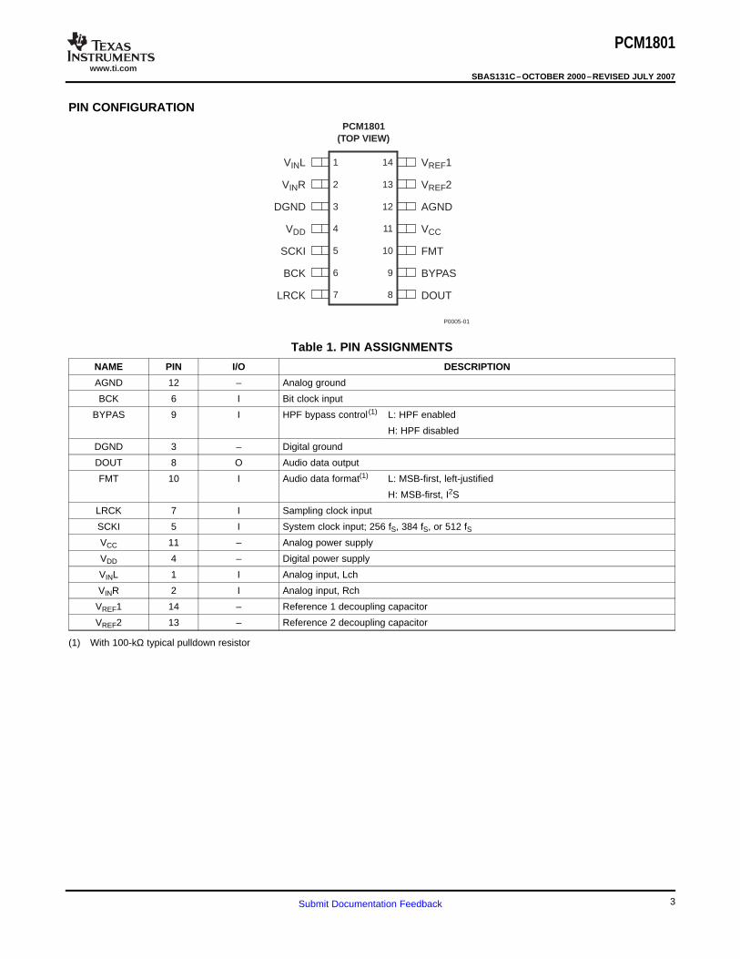
PIN CONFIGURATION
Table 1. PIN ASSIGNMENTS
NAME PIN I/O DESCRIPTION
AGND 12 – Analog ground
BCK 6 I Bit clock input
BYPAS 9 I HPF bypass control (1) L: HPF enabled
H: HPF disabled
DGND 3 – Digital ground
DOUT 8 O Audio data output
FMT 10 I Audio data format(1) L: MSB-first, left-justified
H: MSB-first, I2S
LRCK 7 I Sampling clock input
SCKI 5 I System clock input; 256 fS, 384 fS, or 512 fS
VCC 11 – Analog power supply
VDD 4 – Digital power supply
VINL 1 I Analog input, Lch
VINR 2 I Analog input, Rch
VREF1 14 – Reference 1 decoupling capacitor
VREF2 13 – Reference 2 decoupling capacitor
(1) With 100-kΩ typical pulldown resistor
3Submit Documentation Feedback
www.ti.com
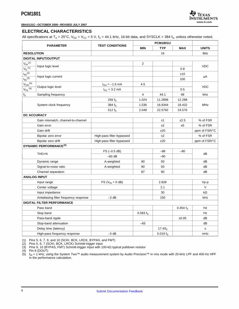
ELECTRICAL CHARACTERISTICS
PCM1801
SBAS131C–OCTOBER 2000–REVISED JULY 2007
All specifications at TA = 25°C, VDD = VCC = 5 V, fS = 44.1 kHz, 16-bit data, and SYSCLK = 384 fS, unless otherwise noted.
PCM1801UPARAMETER TEST CONDITIONS
MIN TYP MAX UNITS
RESOLUTION 16 Bits
DIGITAL INPUT/OUTPUT
VIH(1) 2
Input logic level VDCVIL
(1) 0.8
IIN(2) ±10
Input logic current μAIIN
(3) 100
VOH(4) IOH = –1.6 mA 4.5
Output logic level VDCVOL
(4) IOL = 3.2 mA 0.5
fS Sampling frequency 4 44.1 48 kHz
256 fS 1.024 11.2896 12.288
System clock frequency 384 fS 1.536 16.9344 18.432 MHz
512 fS 2.048 22.5792 24.576
DC ACCURACY
Gain mismatch, channel-to-channel ±1 ±2.5 % of FSR
Gain error ±2 ±5 % of FSR
Gain drift ±20 ppm of FSR/°C
Bipolar zero error High-pass filter bypassed ±2 % of FSR
Bipolar zero drift High-pass filter bypassed ±20 ppm of FSR/°C
DYNAMIC PERFORMANCE (5)
FS (–0.5 dB) –88 –80THD+N dB
–60 dB –90
Dynamic range A-weighted 90 93 dB
Signal-to-noise ratio A-weighted 90 93 dB
Channel separation 87 90 dB
ANALOG INPUT
Input range FS (VIN = 0 dB) 2.828 Vp-p
Center voltage 2.1 V
Input impedance 30 kΩ
Antialiasing filter frequency response –3 dB 150 kHz
DIGITAL FILTER PERFORMANCE
Pass band 0.454 fS Hz
Stop band 0.583 fS Hz
Pass-band ripple ±0.05 dB
Stop-band attenuation –65 dB
Delay time (latency) 17.4/fS s
High-pass frequency response –3 dB 0.019 fS mHz
(1) Pins 5, 6, 7, 9, and 10 (SCKI, BCK, LRCK, BYPAS, and FMT)(2) Pins 5, 6, 7 (SCKI, BCK, LRCK) Schmitt-trigger input(3) Pins 9, 10 (BYPAS, FMT) Schmitt-trigger input with 100-kΩ typical pulldown resistor(4) Pin 8 (DOUT)(5) fIN = 1 kHz, using the System Two™ audio measurement system by Audio Precision™ in rms mode with 20-kHz LPF and 400-Hz HPF
in the performance calculation.
4 Submit Documentation Feedback

www.ti.com
Single-End/DifferentialConverter BCK
VINL
Reference
Single-End/DifferentialConverter
VREF1
VREF2
VINR
5th OrderDelta-SigmaModulator
5th OrderDelta-SigmaModulator
×1/64Decimation
andHigh-Pass
Filter
Power Supply
AGNDVCC VDDDGND
Clock/T iming Control
Serial DataInterface
LRCK
DOUT
FMT
BYPAS
SCKI
(+)
(−)
(−)
(+)
PCM1801
B0004-02
FormatControl
PCM1801
SBAS131C–OCTOBER 2000–REVISED JULY 2007
ELECTRICAL CHARACTERISTICS (continued)All specifications at TA = 25°C, VDD = VCC = 5 V, fS = 44.1 kHz, 16-bit data, and SYSCLK = 384 fS, unless otherwise noted.
PCM1801UPARAMETER TEST CONDITIONS
MIN TYP MAX UNITS
POWER SUPPLY REQUIREMENTS
VCC 4.5 5 5.5Voltage range VDC
VDD 4.5 5 5.5
Supply current (6) VCC = VDD = 5 V 18 24 mA
Power dissipation VCC = VDD = 5 V 90 120 mW
TEMPERATURE RANGE
TA Operation –25 85 °C
Tstg Storage –55 125 °C
θJA Thermal resistance 100 °C/W
(6) No load on DOUT (pin 8)
BLOCK DIAGRAM
5Submit Documentation Feedback

www.ti.com
30 kΩ
1 kΩ
VINL
VREF1
1
14
13
Delta-Sigma Modulator
(+)
VREF
VREF2
+
1 µF
4.7 µF
+4.7 µF
+
+
−
(−)
+
−
1 kΩ
S0011-02
TYPICAL PERFORMANCE CURVES
ANALOG DYNAMIC PERFORMANCE
0.002
0.003
0.004
0.005
0.006
−25 0 25 50 75 100
TA − Free-Air T emperature − °C
TH
D+N
− T
otal
Har
m. D
ist.
+ N
oise
at −
0.5
dB −
%
−0.5 dB
3.0
2.8
2.6
2.2
2.4
−60 dB
G001
TH
D+N
− T
otal
Har
m. D
ist.
+ N
oise
at −
60 d
B −
%
92
93
94
95
96
−25 0 25 50 75 100
TA − Free-Air T emperature − °C
Dyn
amic
Ran
ge −
dB
SNR
96
95
94
92
93
SN
R −
Sig
nal-t
o-N
oise
Rat
io −
dB
G002
Dynamic Range
PCM1801
SBAS131C–OCTOBER 2000–REVISED JULY 2007
ANALOG FRONT-END (Single Channel)
All specifications at TA = 25°C, VDD = VCC = 5 V, fS = 44.1 kHz, and SYSCLK = 384 fS, unless otherwise noted
TOTAL HARMONIC DISTORTION + NOISE DYNAMIC RANGE AND SIGNAL-TO-NOISE RATIOvs vs
TEMPERATURE TEMPERATURE
Figure 1. Figure 2.
6 Submit Documentation Feedback
www.ti.com
0.002
0.003
0.004
0.005
0.006
4.25 4.50 4.75 5.00 5.25 5.50 5.75
VCC − Supply V oltage − V
TH
D+N
− T
otal
Har
m. D
ist.
+ N
oise
at −
0.5
dB −
%
3.0
2.8
2.6
2.2
2.4
TH
D+N
− T
otal
Har
m. D
ist.
+ N
oise
at −
60 d
B −
%
G003
−60 dB
−0.5 dB
92
93
94
95
96
4.25 4.50 4.75 5.00 5.25 5.50 5.75
VCC − Supply V oltage − V
Dyn
amic
Ran
ge −
dB
96
95
94
92
93
SN
R −
Sig
nal-t
o-N
oise
Rat
io −
dB
G004
Dynamic Range
SNR
0.002
0.003
0.004
0.005
0.006
Sampling Rate − kHz
TH
D+N
− T
otal
Har
m. D
ist.
+ N
oise
at −
0.5
dB −
%
3.0
2.8
2.6
2.2
2.4
G005
TH
D+N
− T
otal
Har
m. D
ist.
+ N
oise
at −
60 d
B −
%
4832 44.1
−60 dB
−0.5 dB
92
93
94
95
96
Dyn
amic
Ran
ge −
dB
96
95
94
92
93S
NR
− S
igna
l-to-
Noi
se R
atio
− d
B
G006
Dynamic Range
SNR
Sampling Rate − kHz
4832 44.1
PCM1801
SBAS131C–OCTOBER 2000–REVISED JULY 2007
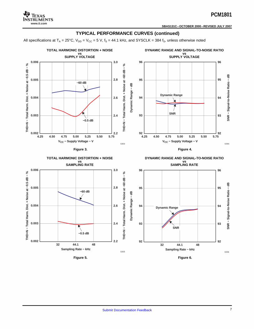
TYPICAL PERFORMANCE CURVES (continued)All specifications at TA = 25°C, VDD = VCC = 5 V, fS = 44.1 kHz, and SYSCLK = 384 fS, unless otherwise noted
TOTAL HARMONIC DISTORTION + NOISE DYNAMIC RANGE AND SIGNAL-TO-NOISE RATIOvs vs
SUPPLY VOLTAGE SUPPLY VOLTAGE
Figure 3. Figure 4.
TOTAL HARMONIC DISTORTION + NOISE DYNAMIC RANGE AND SIGNAL-TO-NOISE RATIOvs vs
SAMPLING RATE SAMPLING RATE
Figure 5. Figure 6.
7Submit Documentation Feedback

www.ti.com
SUPPLY CURRENT
0
4
8
12
16
20
−25 0 25 50 75 100
TA − Free-Air T emperature − °C
I CC
− S
uppl
y C
urre
nt −
mA
IDD
G007
ICC + IDD
ICC
0
4
8
12
16
20
4.25 4.50 4.75 5.00 5.25 5.50 5.75
VCC − Supply V oltage − V
I CC
− S
uppl
y C
urre
nt −
mA
IDD
G008
ICC + IDD
ICC
0
4
8
12
16
20
0 10 20 30 40 50
Sampling Rate − kHz
I CC
− S
uppl
y C
urre
nt −
mA
IDD
G009
ICC + IDD
ICC
PCM1801
SBAS131C–OCTOBER 2000–REVISED JULY 2007
TYPICAL PERFORMANCE CURVES (continued)All specifications at TA = 25°C, VDD = VCC = 5 V, fS = 44.1 kHz, and SYSCLK = 384 fS, unless otherwise noted
SUPPLY CURRENT SUPPLY CURRENTvs vs
TEMPERATURE SUPPLY VOLTAGE
Figure 7. Figure 8.
SUPPLY CURRENTvs
SAMPLING RATE
Figure 9.
8 Submit Documentation Feedback

www.ti.com
OUTPUT SPECTRUM
f − Frequency − kHz
−140
−120
−100
−80
−60
−40
−20
0
0 5 10 15 20
Am
plitu
de −
dB
G010f − Frequency − kHz
−140
−120
−100
−80
−60
−40
−20
0
0 5 10 15 20
Am
plitu
de −
dB
G011
Amplitude − dBV
−100 −80 −60 −40 −20 0
TH
D+N
− T
otal
Har
mon
ic D
isto
rtion
+ N
oise
− %
G012
0.001
0.1
100
0.01
1
10
TH
D+N
− T
otal
Har
mon
ic D
isto
rtion
+ N
oise
− %
f − Frequency − Hz
20 100 1k 20k
G013
10k0.0001
0.01
0.1
0.001
PCM1801
SBAS131C–OCTOBER 2000–REVISED JULY 2007
TYPICAL PERFORMANCE CURVES (continued)All specifications at TA = 25°C, VDD = VCC = 5 V, fS = 44.1 kHz, and SYSCLK = 384 fS, unless otherwise noted
FULL-SCALE FFT –60 dBFS FFT
Figure 10. Figure 11.
TOTAL HARMONIC DISTORTION + NOISE TOTAL HARMONIC DISTORTION + NOISEvs vs
AMPLITUDE FREQUENCY
Figure 12. Figure 13.
9Submit Documentation Feedback

www.ti.com
DECIMATION FILTER
Normalized Frequency [ × fS Hz]
−200
−150
−100
−50
0
0 8 16 24 32
Am
plitu
de −
dB
G014Normalized Frequency [ × fS Hz]
−100
−80
−60
−40
−20
0
0.00 0.25 0.50 0.75 1.00
Am
plitu
de −
dB
G015
Normalized Frequency [ × fS Hz]
−1.0
−0.8
−0.6
−0.4
−0.2
0.0
0.2
0.0 0.1 0.2 0.3 0.4 0.5
Am
plitu
de −
dB
G016Normalized Frequency [ × fS Hz]
−10
−9
−8
−7
−6
−5
−4
−3
−2
−1
0
0.45 0.47 0.49 0.51 0.53 0.55
Am
plitu
de −
dB
G017
−4.13 dB at 0.5 f S
PCM1801
SBAS131C–OCTOBER 2000–REVISED JULY 2007
TYPICAL PERFORMANCE CURVES (continued)All specifications at TA = 25°C, VDD = VCC = 5 V, fS = 44.1 kHz, and SYSCLK = 384 fS, unless otherwise noted
OVERALL CHARACTERISTICS STOP-BAND ATTENUATION CHARACTERISTICS
Figure 14. Figure 15.
PASS-BAND RIPPLE CHARACTERISTICS TRANSITION BAND CHARACTERISTICS
Figure 16. Figure 17.
10 Submit Documentation Feedback

www.ti.com
HIGH-PASS FILTER
Normalized Frequency [ × fS/1000 Hz]
−100
−90
−80
−70
−60
−50
−40
−30
−20
−10
0
0.00 0.05 0.10 0.15 0.20 0.25 0.30 0.35 0.40
Am
plitu
de −
dB
G018Normalized Frequency [ × fS/1000 Hz]
−1.0
−0.8
−0.6
−0.4
−0.2
0.0
0.2
0.0 0.5 1.0 1.5 2.0 2.5 3.0 3.5 4.0
Am
plitu
de −
dB
G019
ANTIALIASING FILTER
−50
−40
−30
−20
−10
0
f − Frequency − Hz
Am
plitu
de −
dB
1 10 100 10M1k 10k
G020
100k 1M−1.0
−0.8
−0.6
−0.4
−0.2
0.0
0.2
f − Frequency − Hz
Am
plitu
de −
dB
1 10 100 100k1k 10k
G021
PCM1801
SBAS131C–OCTOBER 2000–REVISED JULY 2007
TYPICAL PERFORMANCE CURVES (continued)All specifications at TA = 25°C, VDD = VCC = 5 V, fS = 44.1 kHz, and SYSCLK = 384 fS, unless otherwise noted
HIGH-PASS FILTER RESPONSE HIGH-PASS FILTER RESPONSE
Figure 18. Figure 19.
ANTIALIASING FILTER ANTIALIASING FILTERSTOP-BAND CHARACTERISTICS PASS-BAND CHARACTERISTICS
Figure 20. Figure 21.
11Submit Documentation Feedback

www.ti.com
THEORY OF OPERATION
1st
SW-CAPIntegrator
AnalogInX(z) +
−
+− 2nd
SW-CAPIntegrator
3rd
SW-CAPIntegrator
+− 4th
SW-CAPIntegrator
++
++
++
++
5th
SW-CAPIntegrator
DigitalOutY(z)
Comparator
Qn(z)
H(z)
1-BitDAC
STF(z) = H(z) / [1 + H(z)]NTF(z) = 1 / [1 + H(z)]
Y(z) = STF(z) * X(z) + NTF(z) * Qn(z)Signal T ransfer FunctionNoise Transfer Function
B0005-01
SYSTEM CLOCK
PCM1801
SBAS131C–OCTOBER 2000–REVISED JULY 2007
The PCM1801 consists of a band-gap reference, two channels of a single-to-differential converter, a fullydifferential 5th-order delta-sigma modulator, a decimation filter (including digital high-pass), and a serial interfacecircuit. The block diagram illustrates the total architecture of the PCM1801, and the analog front-end diagramillustrates the architecture of the single-to-differential converter and the antialiasing filter. Figure 22 illustrates thearchitecture of the 5th-order delta-sigma modulator and transfer functions.
An internal high-precision reference with two external capacitors provides all reference voltages which arerequired by the converter, and defines the full-scale voltage range of both channels. The internal single-ended todifferential voltage converter saves the design, space, and extra parts needed for external circuitry required bymany delta-sigma converters. The internal full-differential architecture provides a wide dynamic range andexcellent power-supply rejection performance.
The input signal is sampled at a 64× oversampling rate, eliminating the need for a sample-and-hold circuit andsimplifying antialias filtering requirements. The 5th-order delta-sigma noise shaper consists of five integratorswhich use a switched-capacitor topology, a comparator, and a feedback loop consisting of a 1-bitdigital-to-analog converter (DAC). The delta-sigma modulator shapes the quantization noise, shifting it out of theaudio band in the frequency domain. The high order of the modulator enables it to randomize the modulatoroutputs, reducing idle tone levels.
The 64-fS, 1-bit stream from the modulator is converted to 1-fS, 16-bit digital data by the decimation filter, whichalso acts as a low-pass filter to remove the shaped quantization noise. The dc components are removed by adigital high-pass filter, and the filtered output is converted to time-multiplexed serial signals through a serialinterface which provides flexible serial formats.
Figure 22. Simplified Diagram of the PCM1801 5th-Order Delta-Sigma Modulator
The system clock for the PCM1801 must be either 256 fS, 384 fS, or 512 fS, where fS is the audio samplingfrequency. The system clock must be supplied on SCKI (pin 5).
The PCM1801 also has a system clock detection circuit that automatically senses if the system clock isoperating at 256 fS, 384 fS, or 512 fS.
When a 384-fS or 512-fS system clock is used, the PCM1801 automatically divides the clock down to 256 fSinternally. This 256-fS clock is used to operate the digital filter and the modulator. Table 2 lists the relationship oftypical sampling frequencies and system clock frequencies. Figure 23 illustrates the system clock timing.
12 Submit Documentation Feedback

www.ti.com
SCKI0.8 V
2 V
tCLKILtCLKIH
T0005-04
POWER-ON RESET
1024 System Clocks
Reset Reset Removal
4.4 V4 V
3.6 VVCC / VDD
Internal Reset
System Clock
3 Clocks Minimum
DOUT Zero Data Normal Data(1)
18436 / fS
T0014-02
PCM1801
SBAS131C–OCTOBER 2000–REVISED JULY 2007
Table 2. System Clock Frequencies
SAMPLING RATE FREQUENCY SYSTEM CLOCK FREQUENCY(kHz) 256 fs 384 fs 512 fs
32 8.1920 12.2880 16.3840
44.1 11.2896 16.9344 22.5792
48 12.2880 18.4320 24.5760
System clock pulse duration, HIGH t(CLKIH) 12 ns (min)
System clock pulse duration, LOW t(CLKIL) 12 ns (min)
Figure 23. System Clock Timing
The PCM1801 has an internal power-on reset circuit, which initializes (resets) when the supply voltage(VCC/VDD) exceeds 4 V (typical). Because the system clock is used as the clock signal for the reset circuit, thesystem clock must be supplied as soon as power is applied; more specifically, the device must receive at leastthree system clock cycles before VDD > 4 V. While VCC/VDD < 4 V (typical) and for 1024 system clock cycles afterVCC/VDD > 4 V, the PCM1801 stays in the reset state and the digital output is forced to zero. The digital output isvalid 18,436 fS periods after release from the reset state. Figure 24 illustrates the internal power-on reset timingand the digital output for power-on reset.
(1) The transient response (exponentially attenuated signal from ±0.2% dc of FSR with a 200-ms time constant) appearsinitially.
Figure 24. Internal Power-On Reset Timing
13Submit Documentation Feedback

www.ti.com
SERIAL AUDIO DATA INTERFACE
DATA FORMAT
16-Bit, MSB-First, Left-Justified
BCK
LRCK Right-ChannelLeft-Channel
DOUT 114 15 16321
MSB LSB MSB LSB
14 15 16321
LRCK Right-ChannelLeft-Channel
BCK
DOUT
MSB LSB MSB LSB
16-Bit, MSB-First, I 2S
FMT = H
14 15 16321 14 15 16321
FMT = L
T0016-03
PCM1801
SBAS131C–OCTOBER 2000–REVISED JULY 2007
The PCM1801 interfaces the audio system through BCK (pin 6), LRCK (pin 7), and DOUT (pin 8).
The PCM1801 accepts 64-BCK/LRCK, 48-BCK/LRCK (only for a 384-fS system clock) or 32-BCK/LRCK formatfor the left-justified format. And the PCM1801 accepts the 64-BCK/LRCK or 48-BCK/LRCK format (only for a384-fS system clock) for I2S format.
The PCM1801 supports two audio data formats in slave mode, which are selected by the FMT control input(pin 10) as shown in Table 3. Figure 25 illustrates the data format. If the application system cannot ensure aneffective system clock prior to power up of the PCM1801, the FMT pin must be held LOW until the power-onreset sequence is completed. In this case, if the I2S format (FMT = HIGH) is required in the application, FMT canbe set HIGH after the power-on reset sequence is completed.
Table 3. Data Format
FMT DATA FORMAT
0 (L) 16-bit, left-justified
1 (H) 16-bit, I2S
Figure 25. Audio Data Format
14 Submit Documentation Feedback

www.ti.com
INTERFACE TIMING
BCK
LRCK
DOUT
t(BCKH)
t(BCKL)
t(LRHD)
t(LRCP)
t(LRSU)
t(BCKP) t(CKDO) t(LRDO)
1.4 V
1.4 V
0.5 VDD
T0017-02
SYNCHRONIZATION WITH DIGITAL AUDIO SYSTEM
PCM1801
SBAS131C–OCTOBER 2000–REVISED JULY 2007
Figure 26 illustrates the interface timing.
DESCRIPTION SYMBOL MIN TYP MAX UNITS
BCK period t(BCKP) 300 ns
BCK pulse duration, HIGH t(BCKH) 120 ns
BCK pulse duration, LOW t(BCKL) 120 ns
LRCK setup time to BCK rising edge t(LRSU) 80 ns
LRCK hold time to BCK rising edge t(LRHD) 40 ns
LRCK period t(LRCP) 20 μs
Delay time, BCK falling edge to DOUT valid t(CKDO) –20 40 ns
Delay time, LRCK edge to DOUT valid t(LRDO) –20 40 ns
Rising time of all signals t(RISE) 20 ns
Falling time of all signals t(FALL) 20 ns
NOTE: Timing measurement reference level is (VIH + VIL)/2. Rising and falling time ismeasured from 10% to 90% of the I/O signal swing. Load capacitance of the DOUTsignal is 20 pF.
Figure 26. Audio Data Interface Timing
The PCM1801 operates with LRCK synchronized to the system clock (SCKI). The PCM1801 does not require aspecific phase relationship between LRCK and SCKI, but does require the synchronization of LRCK and SCKI. Ifthe relationship between LRCK and SCKI changes more than 6 bit clocks (BCK) during one sample period dueto LRCK or SCKI jitter, internal operation of the ADC halts within 1/fS and the digital output is forced to BPZ untilresynchronization between LRCK and SCKI is completed. In case of changes less than 5 bit clocks (BCK),resynchronization does not occur and the previously described digital output control and discontinuity do notoccur. Figure 27 illustrates the ADC digital output for lost synchronization and resynchronization. Duringundefined data, some noise may be generated in the audio signal. Also, the transition of normal to undefineddata and undefined or zero data to normal makes a discontinuity of data on the digital output and may generatesome noise in the audio signal.
15Submit Documentation Feedback

www.ti.com
1/fS 32/fS
Normal Data(1)Zero DataUndefined
DataNormal Data
SynchronousAsynchronousSynchronous
ResynchronizationSynchronization Lost
DOUT
State of Synchronization
T0020-02
HPF Bypass Control
APPLICATION INFORMATION
BOARD DESIGN AND LAYOUT CONSIDERATIONS
VCC, VDD PINS
AGND, DGND PINS
VIN PINS
VREF PINS
PCM1801
SBAS131C–OCTOBER 2000–REVISED JULY 2007
(1) The transient response (exponentially attenuated signal from ±0.2% dc of FSR with 200-ms time constant) appearsinitially.
Figure 27. ADC Digital Output for Loss of Synchronization and Re-Synchronization
The built-in function for dc component rejection can be bypassed by BYPAS (pin 9) control (see Table 4). Inbypass mode, the dc component of the input analog signal, the internal dc offset, etc., are also converted andoutput in the digital output data.
Table 4. HPF Bypass Control
BYPAS HIGH-PASS FILTER (HPF) MODE
Low Normal (dc cut) mode
High Bypass (through) mode
The digital and analog power supply lines to the PCM1801 should be bypassed to the corresponding groundpins with both 0.1-μF ceramic and 10-μF tantalum capacitors as close to the pins as possible to maximize thedynamic performance of the ADC. Although the PCM1801 has two power lines to maximize the potential ofdynamic performance, using one common power supply is recommended to avoid unexpected power supplyproblems, such as latch-up due to power supply sequencing.
To maximize the dynamic performance of the PCM1801, the analog and digital grounds are not internallyconnected. These points should have low impedance to avoid digital noise feedback into the analog ground.They should be connected directly to each other under the PCM1801 package to reduce potential noiseproblems.
A 1.0-μF tantalum capacitor is recommended as an ac-coupling capacitor, which establishes a 5.3-Hz cutofffrequency. If a higher full-scale input voltage is required, the input voltage range can be increased by adding aseries resistor to the VIN pins.
To ensure low source impedance, 4.7-μF tantalum capacitors are recommended from VREF1 to AGND and fromVREF2 to AGND. These capacitors should be located as close as possible to the VREF1 and VREF2 pins to reducedynamic errors on the ADC references.
16 Submit Documentation Feedback
www.ti.com
DOUT PIN
FMT PIN
SYSTEM CLOCK
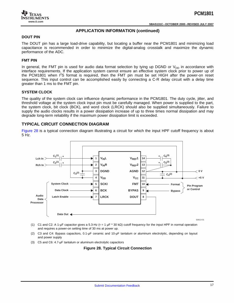
TYPICAL CIRCUIT CONNECTION DIAGRAM
S0013-01
1
2
3
4
5
6
7
14
13
12
11
10
9
8
Format
Latch Enable
Data Out
+
Pin Programor Control
AudioData
Processor
Lch In
+5 VC4(2)
VREF1
VREF2
AGND
VCC
FMT
BYPAS
DOUT
VINL
VINR
DGND
VDD
SCKI
BCK
LRCK
0 V
Bypass
+ C6(3)
+ C5(3)
Data Clock
System Clock
C3(2)
+Rch In
C1(1)
C2(1)
PCM1801
SBAS131C–OCTOBER 2000–REVISED JULY 2007
APPLICATION INFORMATION (continued)
The DOUT pin has a large load-drive capability, but locating a buffer near the PCM1801 and minimizing loadcapacitance is recommended in order to minimize the digital-analog crosstalk and maximize the dynamicperformance of the ADC.
In general, the FMT pin is used for audio data format selection by tying up DGND or VDD in accordance withinterface requirements. If the application system cannot ensure an effective system clock prior to power up ofthe PCM1801 when I2S format is required, then the FMT pin must be set HIGH after the power-on resetsequence. This input control can be accomplished easily by connecting a C-R delay circuit with a delay timegreater than 1 ms to the FMT pin.
The quality of the system clock can influence dynamic performance in the PCM1801. The duty cycle, jitter, andthreshold voltage at the system clock input pin must be carefully managed. When power is supplied to the part,the system clock, bit clock (BCK), and word clock (LRCK) should also be supplied simultaneously. Failure tosupply the audio clocks results in a power dissipation increase of up to three times normal dissipation and maydegrade long-term reliability if the maximum power dissipation limit is exceeded.
Figure 28 is a typical connection diagram illustrating a circuit for which the input HPF cutoff frequency is about5 Hz.
(1) C1 and C2: A 1-μF capacitor gives a 5.3-Hz (τ = 1 μF * 30 kΩ) cutoff frequency for the input HPF in normal operationand requires a power-on setting time of 30 ms at power up.
(2) C3 and C4: Bypass capacitors, 0.1-μF ceramic and 10-μF tantalum or aluminum electrolytic, depending on layoutand power supply
(3) C5 and C6: 4.7-μF tantalum or aluminum electrolytic capacitors
Figure 28. Typical Circuit Connection
17Submit Documentation Feedback

PACKAGE OPTION ADDENDUM
www.ti.com 2-Jul-2013
Addendum-Page 1
PACKAGING INFORMATION
Orderable Device Status(1)
Package Type PackageDrawing
Pins PackageQty
Eco Plan(2)
Lead/Ball Finish MSL Peak Temp(3)
Op Temp (°C) Device Marking(4/5)
Samples
PCM1801U NRND SOIC D 14 50 Green (RoHS& no Sb/Br)
CU NIPDAU Level-1-260C-UNLIM PCM1801U
PCM1801U/2K NRND SOIC D 14 2000 Green (RoHS& no Sb/Br)
CU NIPDAU Level-1-260C-UNLIM PCM1801U
PCM1801U/2KG4 NRND SOIC D 14 2000 Green (RoHS& no Sb/Br)
CU NIPDAU Level-1-260C-UNLIM PCM1801U
PCM1801UG4 NRND SOIC D 14 50 Green (RoHS& no Sb/Br)
CU NIPDAU Level-1-260C-UNLIM PCM1801U
(1) The marketing status values are defined as follows:ACTIVE: Product device recommended for new designs.LIFEBUY: TI has announced that the device will be discontinued, and a lifetime-buy period is in effect.NRND: Not recommended for new designs. Device is in production to support existing customers, but TI does not recommend using this part in a new design.PREVIEW: Device has been announced but is not in production. Samples may or may not be available.OBSOLETE: TI has discontinued the production of the device.
(2) Eco Plan - The planned eco-friendly classification: Pb-Free (RoHS), Pb-Free (RoHS Exempt), or Green (RoHS & no Sb/Br) - please check http://www.ti.com/productcontent for the latest availabilityinformation and additional product content details.TBD: The Pb-Free/Green conversion plan has not been defined.Pb-Free (RoHS): TI's terms "Lead-Free" or "Pb-Free" mean semiconductor products that are compatible with the current RoHS requirements for all 6 substances, including the requirement thatlead not exceed 0.1% by weight in homogeneous materials. Where designed to be soldered at high temperatures, TI Pb-Free products are suitable for use in specified lead-free processes.Pb-Free (RoHS Exempt): This component has a RoHS exemption for either 1) lead-based flip-chip solder bumps used between the die and package, or 2) lead-based die adhesive used betweenthe die and leadframe. The component is otherwise considered Pb-Free (RoHS compatible) as defined above.Green (RoHS & no Sb/Br): TI defines "Green" to mean Pb-Free (RoHS compatible), and free of Bromine (Br) and Antimony (Sb) based flame retardants (Br or Sb do not exceed 0.1% by weightin homogeneous material)
(3) MSL, Peak Temp. -- The Moisture Sensitivity Level rating according to the JEDEC industry standard classifications, and peak solder temperature.
(4) There may be additional marking, which relates to the logo, the lot trace code information, or the environmental category on the device.
(5) Multiple Device Markings will be inside parentheses. Only one Device Marking contained in parentheses and separated by a "~" will appear on a device. If a line is indented then it is a continuationof the previous line and the two combined represent the entire Device Marking for that device.
Important Information and Disclaimer:The information provided on this page represents TI's knowledge and belief as of the date that it is provided. TI bases its knowledge and belief on informationprovided by third parties, and makes no representation or warranty as to the accuracy of such information. Efforts are underway to better integrate information from third parties. TI has taken and

PACKAGE OPTION ADDENDUM
www.ti.com 2-Jul-2013
Addendum-Page 2
continues to take reasonable steps to provide representative and accurate information but may not have conducted destructive testing or chemical analysis on incoming materials and chemicals.TI and TI suppliers consider certain information to be proprietary, and thus CAS numbers and other limited information may not be available for release.
In no event shall TI's liability arising out of such information exceed the total purchase price of the TI part(s) at issue in this document sold by TI to Customer on an annual basis.


IMPORTANT NOTICE
Texas Instruments Incorporated and its subsidiaries (TI) reserve the right to make corrections, enhancements, improvements and otherchanges to its semiconductor products and services per JESD46, latest issue, and to discontinue any product or service per JESD48, latestissue. Buyers should obtain the latest relevant information before placing orders and should verify that such information is current andcomplete. All semiconductor products (also referred to herein as “components”) are sold subject to TI’s terms and conditions of salesupplied at the time of order acknowledgment.
TI warrants performance of its components to the specifications applicable at the time of sale, in accordance with the warranty in TI’s termsand conditions of sale of semiconductor products. Testing and other quality control techniques are used to the extent TI deems necessaryto support this warranty. Except where mandated by applicable law, testing of all parameters of each component is not necessarilyperformed.
TI assumes no liability for applications assistance or the design of Buyers’ products. Buyers are responsible for their products andapplications using TI components. To minimize the risks associated with Buyers’ products and applications, Buyers should provideadequate design and operating safeguards.
TI does not warrant or represent that any license, either express or implied, is granted under any patent right, copyright, mask work right, orother intellectual property right relating to any combination, machine, or process in which TI components or services are used. Informationpublished by TI regarding third-party products or services does not constitute a license to use such products or services or a warranty orendorsement thereof. Use of such information may require a license from a third party under the patents or other intellectual property of thethird party, or a license from TI under the patents or other intellectual property of TI.
Reproduction of significant portions of TI information in TI data books or data sheets is permissible only if reproduction is without alterationand is accompanied by all associated warranties, conditions, limitations, and notices. TI is not responsible or liable for such altereddocumentation. Information of third parties may be subject to additional restrictions.
Resale of TI components or services with statements different from or beyond the parameters stated by TI for that component or servicevoids all express and any implied warranties for the associated TI component or service and is an unfair and deceptive business practice.TI is not responsible or liable for any such statements.
Buyer acknowledges and agrees that it is solely responsible for compliance with all legal, regulatory and safety-related requirementsconcerning its products, and any use of TI components in its applications, notwithstanding any applications-related information or supportthat may be provided by TI. Buyer represents and agrees that it has all the necessary expertise to create and implement safeguards whichanticipate dangerous consequences of failures, monitor failures and their consequences, lessen the likelihood of failures that might causeharm and take appropriate remedial actions. Buyer will fully indemnify TI and its representatives against any damages arising out of the useof any TI components in safety-critical applications.
In some cases, TI components may be promoted specifically to facilitate safety-related applications. With such components, TI’s goal is tohelp enable customers to design and create their own end-product solutions that meet applicable functional safety standards andrequirements. Nonetheless, such components are subject to these terms.
No TI components are authorized for use in FDA Class III (or similar life-critical medical equipment) unless authorized officers of the partieshave executed a special agreement specifically governing such use.
Only those TI components which TI has specifically designated as military grade or “enhanced plastic” are designed and intended for use inmilitary/aerospace applications or environments. Buyer acknowledges and agrees that any military or aerospace use of TI componentswhich have not been so designated is solely at the Buyer's risk, and that Buyer is solely responsible for compliance with all legal andregulatory requirements in connection with such use.
TI has specifically designated certain components as meeting ISO/TS16949 requirements, mainly for automotive use. In any case of use ofnon-designated products, TI will not be responsible for any failure to meet ISO/TS16949.
Products Applications
Audio www.ti.com/audio Automotive and Transportation www.ti.com/automotive
Amplifiers amplifier.ti.com Communications and Telecom www.ti.com/communications
Data Converters dataconverter.ti.com Computers and Peripherals www.ti.com/computers
DLP® Products www.dlp.com Consumer Electronics www.ti.com/consumer-apps
DSP dsp.ti.com Energy and Lighting www.ti.com/energy
Clocks and Timers www.ti.com/clocks Industrial www.ti.com/industrial
Interface interface.ti.com Medical www.ti.com/medical
Logic logic.ti.com Security www.ti.com/security
Power Mgmt power.ti.com Space, Avionics and Defense www.ti.com/space-avionics-defense
Microcontrollers microcontroller.ti.com Video and Imaging www.ti.com/video
RFID www.ti-rfid.com
OMAP Applications Processors www.ti.com/omap TI E2E Community e2e.ti.com
Wireless Connectivity www.ti.com/wirelessconnectivity
Mailing Address: Texas Instruments, Post Office Box 655303, Dallas, Texas 75265Copyright © 2013, Texas Instruments Incorporated