Single-Chip Very Low Power RF Transmitter · Single Chip Very Low Power RF Transmitter ... • Home...
40
CC1050 SWRS044 Page 1 of 40 CC1050 Single Chip Very Low Power RF Transmitter Applications • Very low power UHF wireless data transmitters • 315 / 433 / 868 and 915 MHz ISM/SRD band systems • RKE – Remote Keyless Entry • Home automation • Wireless alarm and security systems • AMR – Automatic Meter Reading • Low power telemetry • Game Controllers and advanced toys Product Description CC1050 is a true single-chip UHF trans- mitter designed for very low power and very low voltage wireless applications. The circuit is mainly intended for the ISM (Industrial, Scientific and Medical) and SRD (Short Range Device) frequency bands at 315, 433, 868 and 915 MHz, but can easily be programmed for operation at other frequencies in the 300-1000 MHz range. The main operating parameters of CC1050 can be programmed via an easy-to- interface serial bus, thus making CC1050 a very flexible and easy to use transmitter. In a typical system CC1050 will be used together with a microcontroller and a few external passive components. CC1050 is based on Chipcon’s SmartRF ® technology in 0.35 µm CMOS. Features • True single chip UHF RF transmitter • Very low current consumption • Frequency range 300 – 1000 MHz • Programmable output power –20 to 12 dBm • Small size (TSSOP-24 package) • Low supply voltage (2.1 V to 3.6 V) • Very few external components required • Single-ended antenna connection • FSK data rate up to 76.8 kBaud • Complies with EN 300 220 and FCC CFR47 part 15 • Programmable frequency in 250 Hz steps makes crystal temperature drift compensation possible without TCXO • Suitable for frequency hopping protocols • Development Kit available • Easy-to-use software for generating the CC1050 configuration data Not Recommended for New Designs
Transcript of Single-Chip Very Low Power RF Transmitter · Single Chip Very Low Power RF Transmitter ... • Home...

CC1050
SWRS044 Page 1 of 40
CC1050 Single Chip Very Low Power RF Transmitter Applications • Very low power UHF wireless data
transmitters • 315 / 433 / 868 and 915 MHz ISM/SRD
band systems
• RKE – Remote Keyless Entry • Home automation • Wireless alarm and security systems • AMR – Automatic Meter Reading • Low power telemetry • Game Controllers and advanced toys
Product Description CC1050 is a true single-chip UHF trans-mitter designed for very low power and very low voltage wireless applications. The circuit is mainly intended for the ISM (Industrial, Scientific and Medical) and SRD (Short Range Device) frequency bands at 315, 433, 868 and 915 MHz, but can easily be programmed for operation at other frequencies in the 300-1000 MHz range. The main operating parameters of CC1050 can be programmed via an easy-to-interface serial bus, thus making CC1050 a very flexible and easy to use transmitter. In a typical system CC1050 will be used together with a microcontroller and a few external passive components.
CC1050 is based on Chipcon’s SmartRF® technology in 0.35 µm CMOS.
Features • True single chip UHF RF transmitter • Very low current consumption • Frequency range 300 – 1000 MHz • Programmable output power –20 to
12 dBm • Small size (TSSOP-24 package) • Low supply voltage (2.1 V to 3.6 V) • Very few external components required • Single-ended antenna connection • FSK data rate up to 76.8 kBaud
• Complies with EN 300 220 and FCC CFR47 part 15
• Programmable frequency in 250 Hz steps makes crystal temperature drift compensation possible without TCXO
• Suitable for frequency hopping protocols
• Development Kit available • Easy-to-use software for generating the
CC1050 configuration data
Not Recommended for New Designs

CC1050
SWRS044 Page 2 of 40
Table of Contents
Absolute Maximum Ratings ....................................................................................................... 4
Operating Conditions ................................................................................................................. 4
Electrical Specifications ............................................................................................................. 4
Pin Assignment .......................................................................................................................... 7
Application Circuit ...................................................................................................................... 9
Configuration Overview............................................................................................................ 10
Configuration Software............................................................................................................. 11
3-wire Serial Configuration Interface........................................................................................ 12
Microcontroller Interface........................................................................................................... 14
Signal interface ........................................................................................................................ 15
Frequency programming .......................................................................................................... 17
VCO ......................................................................................................................................... 17
VCO and PLL self-calibration................................................................................................... 17
VCO current control ................................................................................................................. 21
Power management ................................................................................................................. 21
Output Matching....................................................................................................................... 24
Output power programming ..................................................................................................... 25
Crystal oscillator....................................................................................................................... 26
Optional LC Filter ..................................................................................................................... 27
System Considerations and Guidelines ................................................................................... 28
PCB Layout Recommendations ............................................................................................... 29
Antenna Considerations........................................................................................................... 29
Configuration registers ............................................................................................................. 30
Package Description (TSSOP-24) ........................................................................................... 38
Soldering Information............................................................................................................... 38
Plastic Tube Specification........................................................................................................ 38
Not Recommended for New Designs
CC1050
SWRS044 Page 3 of 40
Carrier Tape and Reel Specification ........................................................................................ 38
Ordering Information ................................................................................................................ 39
General Information ................................................................................................................. 39
Address Information................................................................................................................. 40
Not Recommended for New Designs
CC1050
SWRS044 Page 4 of 40
Absolute Maximum Ratings
Parameter Min. Max. Units Condition Supply voltage, VDD -0.3 5.0 V Voltage on any pin -0.3 VDD+0.3,
max 5.0 V
Input RF level 10 dBm Storage temperature range -50 150 °C Reflow soldering temperature 260 °C T = 10 s
Under no circumstances the absolute maximum ratings given above should be violated. Stress exceeding one or more of
the limiting values may cause permanent damage to the device.
Caution! ESD sensitive device. Precaution should be used when handling the device in order to prevent permanent damage.
Operating Conditions
Parameter
Min. Typ. Max. Unit Condition / Note
RF Frequency Range 300
1000 MHz Programmable in steps of 250 Hz
Operating ambient temperature range -40 85 °C
Supply voltage
2.1 3.0 3.6 V
Note: The same supply voltage should be used for digital (DVDD) and analogue (AVDD) power.
Electrical Specifications Tc = 25°C, VDD = 3.0 V if nothing else stated
Parameter
Min. Typ. Max. Unit Condition / Note
Transmit Section
Transmit data rate
0.6 76.8 kBaud NRZ or Manchester encoding. 76.8 kBaud equals 76.8 kbit/s using NRZ coding. See page 15.
Binary FSK frequency separation
0 65 kHz The frequency separation is programmable in 250 Hz steps. 65 kHz is the maximum guaranteed separation at 1 MHz reference frequency. Larger separations can be achieved at higher reference frequencies.
Output power 433 MHz 868 MHz
-20 -20
12 8
dBm dBm
Delivered to 50 Ω load. The output power is programmable.
RF output impedance 433/868 MHz
110 / 70 Ω Transmit mode. For matching details see p.24.
Not Recommended for New Designs

CC1050
SWRS044 Page 5 of 40
Parameter
Min. Typ. Max. Unit Condition / Note
Spurious emission -36 dBm Complies with EN 300 220
Harmonics
-20 dBc An external LC should be used to reduce harmonics emission to comply with SRD requirements. See p.27.
Frequency Synthesiser Section
Crystal Oscillator Frequency
3 16 MHz Crystal frequency can be 3-4, 6-8 or 9-16 MHz. Recommended frequencies are 3.6864, 7.3728, 11.0592 and 14.7456. See page 26 for details.
Crystal frequency accuracy requirement
± 50 ± 25
ppm 433 MHz 868 MHz The crystal frequency accuracy and drift (ageing and temperature dependency) will determine the frequency accuracy of the transmitted signal.
Crystal operation
Parallel
C3 and C4 are loading capacitors, see page 26
Crystal load capacitance
12 12 12
22 16 16
30 30 16
pF pF pF
3-8 MHz, 22 pF recommended 6-8 MHz, 16 pF recommended 9-16 MHz, 16 pF recommended
Crystal oscillator start-up time 4 1.5 2
ms ms ms
3.6864 MHz, 16 pF load 7.3728 MHz, 16 pF load 16 MHz, 16 pF load
Output signal phase noise
-80 dBc/Hz At 100 kHz offset from carrier
PLL lock time
200 µs Up to 1 MHz frequency step
PLL turn-on time, crystal oscillator on in power down mode
250 µs Crystal oscillator running
Digital Inputs/Outputs
Logic "0" input voltage
0 0.3*VDD V
Logic "1" input voltage
0.7*VDD VDD V
Logic "0" output voltage 0
0.4 V Output current -2.5 mA, 3.0 V supply voltage
Logic "1" output voltage 2.5
VDD V Output current 2.5 mA, 3.0 V supply voltage
Logic "0" input current
NA -1 µA Input signal equals GND
Logic "1" input current
NA 1 µA Input signal equals VDD
DI setup time 20 ns TX mode, minimum time DI must be ready before the positive edge of DCLK
DI hold time
10 ns TX mode, minimum time DI must be held after the positive edge of DCLK
Not Recommended for New Designs

CC1050
SWRS044 Page 6 of 40
Parameter
Min. Typ. Max. Unit Condition / Note
Serial interface (PCLK, PDATA and PALE) timing specification
See Table 2 page 13
Current Consumption
Power Down mode
0.2 1 µA Oscillator core off
Current Consumption, transmit mode 433/868 MHz: P=0.01mW (-20dBm) P=0.3mW (-5dBm) P=1mW (0dBm) P=3mW (5dBm) P=6mW (8dBm) P=16mW (12dBm)
5.5/8.0
7.3/10.0
9.1/14.2
13.3/17.7
15.9/24.9
23.3/NA
mA
mA
mA
mA
mA
mA
The output power is delivered to a 50Ω load
Current Consumption, crystal osc. Current Consumption, crystal osc. and bias Current Consumption, crystal osc., bias and synthesiser
30 80
105
400
4.0 5.5
µA µA µA
µA
mA mA
3-8 MHz, 16 pF load 9-14 MHz, 12 pF load 14-16 MHz, 16 pF load < 500 MHz > 500 MHz
Not Recommended for New Designs

CC1050
SWRS044 Page 7 of 40
Pin Assignment
Pin no. Pin name Pin type Description 1 AVDD Power (A) Power supply (3 V) for analog modules (PA) 2 AGND Ground (A) Ground connection (0 V) for analog modules (PA) 3 AGND Ground (A) Ground connection (0 V) for analog modules (PA) 4 AGND Ground (A) Ground connection (0 V) for analog modules (VCO and prescaler) 5 L1 Analog input Connection no 1 for external VCO tank inductor 6 L2 Analog input Connection no 2 for external VCO tank inductor 7 AVDD Power (A) Power supply (3 V) for analog modules (VCO and prescaler) 8 CHP_OUT Analog output Charge pump current output when external loop filter is used
The pin can also be used as PLL Lock indicator. Output is high when PLL is in lock.
9 R_BIAS Analog output Connection for external precision bias resistor (82 kΩ, ± 1%) 10 AGND Ground (A) Ground connection (0 V) for analog modules (backplane) 11 AVDD Power (A) Power supply (3 V) for analog modules (general) 12 AGND Ground (A) Ground connection (0 V) for analog modules (general) 13 XOSC_Q2 Analog output Crystal, pin 2 14 XOSC_Q1 Analog input Crystal, pin 1, or external clock input 15 AGND Ground (A) Ground connection (0 V) for analog modules (guard) 16 DGND Ground (D) Ground connection (0 V) for digital modules (substrate) 17 DVDD Power (D) Power supply (3 V) for digital modules 18 DGND Ground (D) Ground connection (0 V) for digital modules 19 DI Digital input Data input in transmit mode 20 DCLK Digital output Clock for data in transmit mode 21 PCLK Digital input Programming clock for 3-wire bus 22 PDATA Digital
input/output Programming data for 3-wire bus. Programming data input for write operation, programming data output for read operation
23 PALE Digital input Programming address latch enable for 3-wire bus 24 RF_OUT RF output RF signal output to antenna
A=Analog, D=Digital
(Top View)
AGND
AGND
AGND
L1
L2
AVDD
AGND
CC1050
1
2
3
5
4
6
7
8
10
11
12
9
PALE
PDATA
PCLK
DCLK
DI
DGND
DVDD
DGND
AGND
XOSC_Q1
AGND XOSC_Q2
24
23
22
20
21
19
18
17
15
14
13
16
RF_OUTAVDD
CHP_OUT
R_BIAS
AVDD
AGND
AGND
AGND
L1
L2
AVDD
AGND
CC1050
1
2
3
5
4
6
7
8
10
11
12
9
PALE
PDATA
PCLK
DCLK
DI
DGND
DVDD
DGND
AGND
XOSC_Q1
AGND XOSC_Q2
24
23
22
20
21
19
18
17
15
14
13
16
RF_OUTAVDD
CHP_OUT
R_BIAS
AVDD
Not Recommended for New Designs
CC1050
SWRS044 Page 8 of 40
Circuit Description
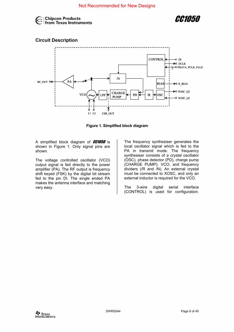
Figure 1. Simplified block diagram
A simplified block diagram of CC1050 is shown in Figure 1. Only signal pins are shown. The voltage controlled oscillator (VCO) output signal is fed directly to the power amplifier (PA). The RF output is frequency shift keyed (FSK) by the digital bit stream fed to the pin DI. The single ended PA makes the antenna interface and matching very easy.
The frequency synthesiser generates the local oscillator signal which is fed to the PA in transmit mode. The frequency synthesiser consists of a crystal oscillator (OSC), phase detector (PD), charge pump (CHARGE PUMP), VCO, and frequency dividers (/R and /N). An external crystal must be connected to XOSC, and only an external inductor is required for the VCO. The 3-wire digital serial interface (CONTROL) is used for configuration.
PDATA, PCLK, PALE
PA
VCO PD OSC~/N
CHARGEPUMP
L1
DI
CHP_OUT
RF_OUT
3
CONTROL
XOSC_Q2
XOSC_Q1/R
DCLK
L2
LPF
BIAS R_BIAS
PDATA, PCLK, PALE
PA
VCO PD OSC~/N
CHARGEPUMP
L1
DI
CHP_OUT
RF_OUT
3
CONTROL
XOSC_Q2
XOSC_Q1/R
DCLK
L2
LPF
BIAS R_BIAS
Not Recommended for New Designs
CC1050
SWRS044 Page 9 of 40
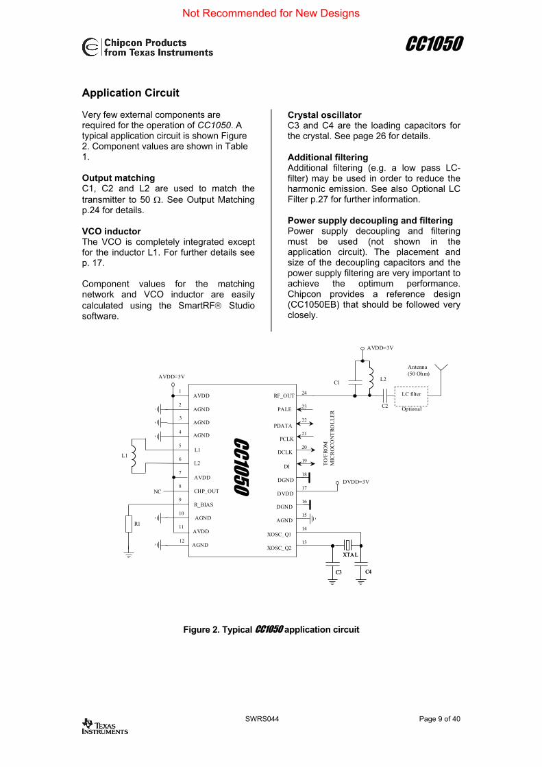
Application Circuit Very few external components are required for the operation of CC1050. A typical application circuit is shown Figure 2. Component values are shown in Table 1. Output matching C1, C2 and L2 are used to match the transmitter to 50 Ω. See Output Matching p.24 for details. VCO inductor The VCO is completely integrated except for the inductor L1. For further details see p. 17. Component values for the matching network and VCO inductor are easily calculated using the SmartRF® Studio software.
Crystal oscillator C3 and C4 are the loading capacitors for the crystal. See page 26 for details. Additional filtering Additional filtering (e.g. a low pass LC-filter) may be used in order to reduce the harmonic emission. See also Optional LC Filter p.27 for further information. Power supply decoupling and filtering Power supply decoupling and filtering must be used (not shown in the application circuit). The placement and size of the decoupling capacitors and the power supply filtering are very important to achieve the optimum performance. Chipcon provides a reference design (CC1050EB) that should be followed very closely.
Figure 2. Typical CC1050 application circuit
LC filter
11
12
RF_OUT
AGND
AGND
AGND
L1
AVDD
L2
R_BIAS
CHP_OUT
AGND
PALE
PDATA
PCLK
DCLK
DI
DVDD
DGND
AGND
XOSC_Q1
AGND XOSC_Q2
AVDD
L1
TO/F
ROM
MIC
RO
CO
NT
ROLL
ER
1
3
2
4
5
6
8
9
10
7
24
23
22
20
21
19
18
17
15
14
13
16
C4C4C3C3
Antenna(50 Ohm)
CC1050
AVDD=3V
DVDD=3V
Optional
XTALXTAL
NC
L2C1
C2
AVDD=3V
R1
DGNDAVDD
Not Recommended for New Designs

CC1050
SWRS044 Page 10 of 40
Item 315 MHz 433 MHz 868 MHz 915 MHz
C1 5.6 pF, 5%, C0G, 0603 12 pF, 5%, C0G, 0603 4.7 pF, 5%, C0G, 0603 4.7 pF, 5%, C0G, 0603 C2 8.2 pF, 5%, C0G, 0603 6.8 pF, 5%, C0G, 0603 5.6 pF, 5%, C0G, 0603 5.6 pF, 5%, C0G, 0603 C3* 15 pF, 5%, C0G, 0603 15 pF, 5%, C0G, 0603 15 pF, 5%, C0G, 0603 15 pF, 5%, C0G, 0603 C4* 15 pF, 5%, C0G, 0603 15 pF, 5%, C0G, 0603 15 pF, 5%, C0G, 0603 15 pF, 5%, C0G, 0603 L1 56 nH, 5%, 0603 33 nH, 5%, 0603 5.6 nH, 5%, 0603 5.6 nH, 5%, 0603 L2 20 nH, 10%, 0805 6.2 nH, 10%, 0805 2.5 nH, 10%, 0805 2.5 nH, 10%, 0805 R1 82 kΩ, 1%, 0603 82 kΩ, 1%, 0603 82 kΩ, 1%, 0603 82 kΩ, 1%, 0603 XTAL 14.7456 MHz crystal,
16 pF load 14.7456 MHz crystal, 16 pF load
14.7456 MHz crystal, 16 pF load
14.7456 MHz crystal, 16 pF load
Notes: Items shaded are different for different frequencies. Component values for 868 and 915 MHz are equal. *) C3 and C4 will depend on the crystal load capacitance, see page 26.
Table 1. Bill of materials for the application circuit
Configuration Overview CC1050 can be configured to achieve the best performance for different applications. Through the programmable configuration registers the following key parameters can be programmed: • Transmit mode / power-down / power-
up mode • RF output power • Frequency synthesiser key
parameters: RF output frequency, FSK
frequency separation (deviation), crystal oscillator reference frequency
• Crystal oscillator power-up / power down
• Data rate and data format (NRZ, Manchester coded or UART interface)
• Synthesiser lock indicator mode • Modulation spectrum shaping
Not Recommended for New Designs

CC1050
SWRS044 Page 11 of 40
Configuration Software Chipcon provides users of CC1050 with a software program, SmartRF® Studio (Windows interface) that generates all necessary CC1050 configuration data based on the user's selections of various parameters. These hexadecimal numbers will then be the necessary input to the microcontroller for the configuration of
CC1050. In addition the program will provide the user with the component values needed for the output matching circuit and the VCO inductor. Figure 3 shows the user interface of the CC1050 configuration software.
Figure 3. SmartRF® Studio user interface
Not Recommended for New Designs

CC1050
SWRS044 Page 12 of 40
3-wire Serial Configuration Interface CC1050 is configured via a simple 3-wire interface (PDATA, PCLK and PALE). There are 19 8-bit configuration registers, each addressed by a 7-bit address. A Read/Write bit initiates a read or write operation. A full configuration of CC1050 requires sending 19 data frames of 16 bits each (7 address bits, R/W bit and 8 data bits). The time needed for a full configuration depend on the PCLK frequency. With a PCLK frequency of 10 MHz the full configuration is done in less than 30 µs. Setting the device in power down mode requires sending one frame only and will in this case take less than 2 µs. All registers are also readable. In each write-cycle 16 bits are sent on the PDATA-line. The seven most significant bits of each data frame (A6:0) are the address-bits. A6 is the MSB (Most Significant Bit) of the address and is sent as the first bit. The next bit is the R/W bit (high for write, low for read). During address and R/W bit transfer the PALE (Program Address Latch Enable) must be kept low. The 8 data-bits are then transferred (D7:0). See Figure 4.
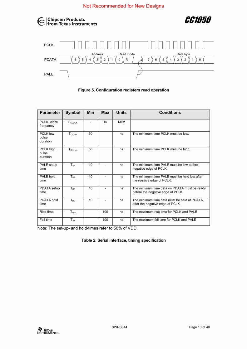
The timing for the programming is also shown in Figure 4 with reference to Table 2. The clocking of the data on PDATA is done on the negative edge of PCLK. When the last bit, D0, of the 8 data-bits has been loaded, the data word is loaded in the internal configuration register. The configuration data is stored in internal RAM and is valid after power-down mode, but not when the power-supply is turned off. The registers can be programmed in any order. The configuration registers can also be read by the microcontroller via the same configuration interface. The seven address bits are sent first, then the R/W bit set low to initiate the data read-back. CC1050 then returns the data from the addressed register. PDATA is in this case used as an output and must be tri-stated (or set high n the case of an open collector pin) by the microcontroller during the data read-back (D7:0). The read operation is illustrated in Figure 5.
Figure 4. Configuration registers write operation
PCLK
PDATA
PALE
Address Write mode
6 5 4 3 2 1 0 7 6 5 4 3 2 1 0
Data byte
THD
TSA
TCH,min TCL,min
THA
W
TSDTSA
Not Recommended for New Designs
CC1050
SWRS044 Page 13 of 40
Figure 5. Configuration registers read operation
Parameter Symbol
Min Max Units Conditions
PCLK, clock frequency
FCLOCK
- 10 MHz
PCLK low pulse duration
TCL,min 50 ns The minimum time PCLK must be low.
PCLK high pulse duration
TCH,min 50 ns The minimum time PCLK must be high.
PALE setup time
TSA
10 - ns The minimum time PALE must be low before negative edge of PCLK.
PALE hold time
THA 10 - ns The minimum time PALE must be held low after the positive edge of PCLK.
PDATA setup time
TSD
10 - ns The minimum time data on PDATA must be ready before the negative edge of PCLK.
PDATA hold time
THD 10 - ns The minimum time data must be held at PDATA, after the negative edge of PCLK.
Rise time Trise 100 ns The maximum rise time for PCLK and PALE
Fall time Tfall 100 ns The maximum fall time for PCLK and PALE
Note: The set-up- and hold-times refer to 50% of VDD.
Table 2. Serial interface, timing specification
PCLK
Address Read mode
6 5 4 3 2 1 0 R 7 6 5 4 3 2 1 0
Data byte
PALE
PDATA
Not Recommended for New Designs

CC1050
SWRS044 Page 14 of 40
Microcontroller Interface Used in a typical system, CC1050 will interface to a microcontroller. This microcontroller must be able to: • Program CC1050 into different modes
via the 3-wire serial configuration interface (PDATA, PCLK and PALE).
• Interface to the synchronous data signal interface (DI and DCLK).
• Optionally the microcontroller can do data encoding / decoding.
• Optionally the microcontroller can monitor the frequency lock status from pin CHP_OUT (LOCK).
Connecting the microcontroller The microcontroller uses 3 output pins for the configuration interface (PDATA, PCLK and PALE). PDATA should be a bi-directional pin for data read-back. The DI pin is used for data to be transmitted. DCLK providing the data timing should be connected to a microcontroller input. Optionally another pin can be used to monitor the LOCK signal (available at the CHP_OUT pin). This signal is logic level high when the PLL is in lock. See Figure 6.
The microcontroller pins connected to PDATA and PCLK can be used for other purposes when the configuration interface is not used. PDATA and PCLK are high impedance inputs as long as PALE high. PALE has an internal pull-up resistor and should be left open (tri-stated by the microcontroller) or set to a high level during power down mode in order to prevent a trickle current flowing in the pull-up.
CC1050
PDATAPCLKPALE
DI
CHP_OUT(LOCK)
Micro-controller
DCLK(Optional)
CC1050
PDATAPCLKPALE
DI
CHP_OUT(LOCK)
Micro-controller
DCLK(Optional)
Figure 6. Microcontroller interface
Not Recommended for New Designs

CC1050
SWRS044 Page 15 of 40
Signal interface The signal interface consists of DI and DCLK and is used for the data to be transmitted. DI is the data input line and DCLK provides a synchronous clock during data transmission. The CC1050 can be used with NRZ (Non-Return-to-Zero) data or Manchester (also known as bi-phase-level) encoded data. CC1050 can be configured for three different data formats: Synchronous NRZ mode. CC1050 provides the data clock at DCLK, and DI is used as data input. Data is clocked into CC1050 at the rising edge of DCLK. The data is modulated at RF without encoding. CC1050 can be configured for the data rates 0.6, 1.2, 2.4, 4.8, 9.6, 19.2, 38.4 or 76.8 kbit/s. See Figure 7. Synchronous Manchester encoded mode. CC1050 provides the data clock at DCLK, and DI is used as data input. Data is clocked into CC1050 at the rising edge of DCLK and should be in NRZ format. The data is modulated at RF with Manchester code. The encoding is done by CC1050. In this mode CC1050 can be configured for
the data rates 0.3, 0.6, 1.2, 2.4, 4.8, 9.6, 19.2 or 38.4 kbit/s. The 38.4 kbit/s rate corresponds to the maximum 76.8 kBaud due to the Manchester encoding. See Figure 8. Transparent Asynchronous UART mode. In transmit mode DI is used as data input. The data is modulated at RF without synchronisation or encoding. Data rates in the range from 0.6 to 76.8 kBaud can be used. See Figure 9. Manchester encoding In the Synchronous Manchester encoded mode CC1050 uses Manchester coding when modulating the data. The Manchester code is based on transitions; a “0” is encoded as a low-to-high transition, a “1” is encoded as a high-to-low transition. See Figure 10. The Manchester code ensures that the signal has a constant DC component, which is necessary in some FSK demodulators. Using this mode also ensures compatibility with CC400/CC900 designs.
DCLK
DI
“RF”
Clock provided by CC1050
FSK modulating signal (NRZ),internal in CC1050
Data provided by microcontroller
DCLK
DI
“RF”
Clock provided by CC1050
FSK modulating signal (NRZ),internal in CC1050
Data provided by microcontroller
Figure 7. Synchronous NRZ mode
Not Recommended for New Designs

CC1050
SWRS044 Page 16 of 40
DCLK
DI
“RF”
Clock provided by CC1050
FSK modulating signal (Manchester encoded),internal in CC1050
Data provided by microcontroller (NRZ)
DCLK
DI
“RF”
Clock provided by CC1050
FSK modulating signal (Manchester encoded),internal in CC1050
Data provided by microcontroller (NRZ)
Figure 8. Synchronous Manchester encoded mode
DCLK
DI
“RF”
DCLK is not used
FSK modulating signal,internal in CC1050
Data provided by UART (TXD)
DCLK
DI
“RF”
DCLK is not used
FSK modulating signal,internal in CC1050
Data provided by UART (TXD)
Figure 9. Transparent Asynchronous UART mode
Time
TXdata
1 0 1 1 0 0 0 1 1 0 1
Time
TXdata
1 0 1 1 0 0 0 1 1 0 1
Figure 10. Manchester encoding
Not Recommended for New Designs

CC1050
SWRS044 Page 17 of 40
Frequency programming The operation frequency is set by programming the frequency word in the configuration registers. There are two frequency words registers, termed A and B, which can be programmed to two different frequencies in order to switch fast between two different channels. Frequency word A or B is selected by the F_REG bit in the MAIN register. The frequency word is 24 bits (3 bytes) located in FREQ_2A:FREQ_1A:FREQ_0A and FREQ_2B:FREQ_1B:FREQ_0B for the A and B word respectively. The FSK frequency separation is programmed in the FSEP1:FSEP0 registers (11 bits). The frequency word FREQ is calculated by:
163848192+
⋅=FREQff refVCO
where the reference frequency is the crystal oscillator clock divided by REFDIV (4 bits in the PLL register), a number between 2 and 15:
REFDIVf
f xoscref =
The equation above gives the VCO frequency, that is, fVCO is the f0 frequency for transmit mode (lower FSK frequency). The upper FSK frequency is given by: f1 = f0 + fsep where fsep is set by the separation word:
16384FSEPff refsep ⋅=
VCO Only one external inductor (L1) is required for the VCO. The inductor will determine the operating frequency range of the circuit. It is important to place the inductor as close to the pins as possible in order to reduce stray inductance. It is recommended to use a high Q, low tolerance inductor for best performance.
Typical tuning range for the integrated varactor is 20-25%. Component values for various frequencies are given in Table 1. Component values for other frequencies can be found using the SmartRF® Studio software.
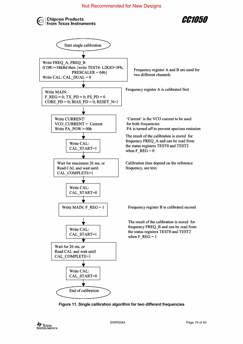
VCO and PLL self-calibration To compensate for supply voltage, temperature and process variations the VCO and PLL must be calibrated. The calibration is done automatically and sets maximum VCO tuning range and optimum charge pump current for PLL stability. After setting up the device at the operating frequency, the self-calibration can be initiated by setting the CAL_START bit. The calibration result is stored internally in the chip, and is valid as long as power is not turned off. If large supply voltage variations (more than 0.5 V) or temperature variations (more than 40 degrees) occur after calibration, a new calibration should be performed.
The self-calibration is controlled through the CAL register (see configuration registers description p. 30). The CAL_COMPLETE bit indicates complete calibration. The user can poll this bit, or simply wait for 26 ms (calibration wait time when CAL_WAIT = 1). The wait time is proportional to the internal PLL reference frequency. The lowest permitted reference frequency (1 MHz) gives 26 ms wait time, which is therefore the worst case.
Reference frequency [MHz]
Calibration time [ms]
2.4 11 2.0 13 1.5 18 1.0 26
Not Recommended for New Designs

CC1050
SWRS044 Page 18 of 40
The CAL_COMPLETE bit can also be monitored at the CHP_OUT (LOCK) pin (configured by LOCK_SELECT[3:0]) and used as an interrupt input to the microcontroller. The CAL_START bit must be set to 0 by the microcontroller after the calibration is done. There are separate calibration values for the two frequency registers. If the two frequencies, A and B, differ more than 1
MHz, or different VCO currents are used (VCO_CURRENT[3:0] in the CURRENT register) the calibration should be done separately. The CAL_DUAL bit in the CAL register controls dual or separate calibration. The single calibration algorithm using separate calibration for two frequencies is illustrated in Figure 11. In Figure 12 the dual calibration algorithm is shown.
Not Recommended for New Designs
CC1050
SWRS044 Page 19 of 40
Write CAL:CAL_START=0
End of calibration
Wait for maximum 26 ms, or Read CAL and wait until CAL_COMPLETE=1
Start single calibration
Frequency register A is calibrated firstWrite MAIN:F_REG = 0; TX_PD = 0; FS_PD = 0CORE_PD = 0; BIAS_PD = 0; RESET_N=1
Write FREQ_A, FREQ_BIf DR>=38kBd then write TEST4: L2KIO=3Fh,
PRESCALER = 04hWrite CAL: CAL_DUAL = 0
Frequency register A and B are used for two different channels
Write CAL:CAL_START=1
The result of the calibration is stored forfrequency FREQ_A and can be read from the status registers TEST0 and TEST2when F_REG = 0
Write CURRENT:VCO_CURRENT = CurrentWrite PA_POW = 00h
‘Current’ is the VCO current to be usedfor both frequenciesPA is turned off to prevent spurious emission
Write CAL:CAL_START=0
Wait for 26 ms, or Read CAL and wait until CAL_COMPLETE=1
Frequency register B is calibrated secondWrite MAIN: F_REG = 1
Write CAL:CAL_START=1
Calibration time depend on the reference frequency, see text.
The result of the calibration is stored forfrequency FREQ_B and can be read from the status registers TEST0 and TEST2when F_REG = 1
Write CAL:CAL_START=0
End of calibration
Wait for maximum 26 ms, or Read CAL and wait until CAL_COMPLETE=1
Start single calibration
Frequency register A is calibrated firstWrite MAIN:F_REG = 0; TX_PD = 0; FS_PD = 0CORE_PD = 0; BIAS_PD = 0; RESET_N=1
Write FREQ_A, FREQ_BIf DR>=38kBd then write TEST4: L2KIO=3Fh,
PRESCALER = 04hWrite CAL: CAL_DUAL = 0
Frequency register A and B are used for two different channels
Write CAL:CAL_START=1
The result of the calibration is stored forfrequency FREQ_A and can be read from the status registers TEST0 and TEST2when F_REG = 0
Write CURRENT:VCO_CURRENT = CurrentWrite PA_POW = 00h
‘Current’ is the VCO current to be usedfor both frequenciesPA is turned off to prevent spurious emission
Write CAL:CAL_START=0
Wait for 26 ms, or Read CAL and wait until CAL_COMPLETE=1
Frequency register B is calibrated secondWrite MAIN: F_REG = 1
Write CAL:CAL_START=1
Calibration time depend on the reference frequency, see text.
The result of the calibration is stored forfrequency FREQ_B and can be read from the status registers TEST0 and TEST2when F_REG = 1
Figure 11. Single calibration algorithm for two different frequencies
Not Recommended for New Designs

CC1050
SWRS044 Page 20 of 40
Write CAL:CAL_START=0
End of calibration
Wait for maximum 26 ms, or Read CAL and wait until CAL_COMPLETE=1
Start dual calibration
Either frequency register A or B is selectedWrite MAIN:F_REG = 0TX_PD = 0; FS_PD = 0CORE_PD = 0; BIAS_PD = 0; RESET_N=1
Write FREQ_A, FREQ_BIf DR>=38kBd then write TEST4: L2KIO=3Fh,
PRESCALER = 04hWrite CAL: CAL_DUAL = 1
Frequency registers A and B are both used
Write CAL:CAL_START=1
The result of the calibration is stored forBoth frequency FREQ_A and FREQ_B, andcan be read from the status registers TEST0 and TEST2
Write CURRENT:VCO_CURRENT = CurrentWrite PA_POW = 00h
‘Current’ is the VCO current to be used for both frequencies
Calibration time depend on the reference frequency, see text.
Figure 12. Dual calibration algorithm
Not Recommended for New Designs

CC1050
SWRS044 Page 21 of 40
VCO current control The VCO current is programmable and should be set according to operating frequency and output power. Recommended settings for the VCO_CURRENT bits in the CURRENT register are shown in the tables on page 32.
The bias current for the PA buffers are also programmable. Recommended settings for the PA_DRIVE bits in the CURRENT register are shown in the tables on page 32.
Power management CC1050 offers great flexibility for power management in order to meet strict power consumption requirements in battery operated applications. Power Down mode is controlled through the MAIN register. There are separate bits to control the TX part, the frequency synthesiser and the crystal oscillator. This individual control can be used to optimise for lowest possible current consumption in a certain application.
A typical power-on and initialising sequence for minimum power consumption is shown in Figure 13 and Figure 14. PALE should be tri-stated or set to a high level during power down mode in order to prevent a trickle current from flowing in the internal pull-up resistor. PA_POW should be set to 00h during power down mode to ensure lowest possible leakage current.
Not Recommended for New Designs

CC1050
SWRS044 Page 22 of 40
Power Down
Power OffPower turned on
Initialise and reset:MAIN:F_REG = 0TX_PD = 1FS_PD = 1CORE_PD = 0BIAS_PD = 1RESET_N = 0
Program all registers except MAIN
Calibrate VCO and PLL Calibration is performed according to calibration algorithm
MAIN: RESET_N = 1Wait 2 ms*
Reset and turn on the crystal oscillator core
*Time to wait depends on the crystal frequency and the load capacitance
PA_POW = 00h MAIN: TX_PD = 1, FS_PD = 1, CORE_PD = 1, BIAS_PD = 1
Figure 13. Initializing sequence
Not Recommended for New Designs

CC1050
SWRS044 Page 23 of 40
Turn on crystal oscillator coreMAIN: CORE_PD = 0Wait 2 ms*
Turn on bias generatorBIAS_PD = 0Wait 200 µs
Power Down
*Time to wait depends on the crystal frequency and the load capacitance
Turn on TX: PA_POW = 00hMAIN: F_REG = 1 FS_PD = 0Wait 250 µs
TX mode
Turn off TX: PA_POW = 00hMAIN: TX_PD = 1, FS_PD = 1, CORE_PD=1, BIAS_PD=1
Power Down
TX_PD = 0 PA_POW = ‘Output power’Wait 20 µs
Waiting for the PLL to lock
Waiting for the PA to ramp up
Figure 14. Sequence for activating TX mode
Not Recommended for New Designs

CC1050
SWRS044 Page 24 of 40
Output Matching A few passive external components ensures match in TX mode. The matching network is shown in Figure 15. Component values for various frequencies
are given in Table 1. Component values for other frequencies can be found using the configuration software.
Figure 15. Output matching network
RF_OUTTO ANTENNA
CC1050
L2C1
C2
AVDD=3V
Not Recommended for New Designs

CC1050
SWRS044 Page 25 of 40
Output power programming
The RF output power is programmable and controlled by the PA_POW register. Table 3 shows the closest programmable value for output powers in steps of 1 dB. The typical current consumption is also shown.
In power down mode the PA_POW should be set to 00h for minimum leakage current.
RF frequency 433 MHz RF frequency 868 MHz Output power [dBm] PA_POW
[hex] Current consumption, typ. [mA]
PA_POW [hex]
Current consumption, typ. [mA]
-20 01 5.5 02 8.0 -19 01 5.5 02 8.0 -18 01 5.5 02 8.0 -17 02 5.7 03 8.3 -16 02 5.7 03 8.3 -15 02 5.7 04 8.5 -14 02 5.7 04 8.5 -13 03 6.0 05 8.7 -12 03 6.0 05 8.7 -11 04 6.2 06 8.9 -10 04 6.2 06 8.9 -9 05 6.5 07 9.1 -8 05 6.5 08 9.4 -7 06 6.8 09 9.6 -6 07 7.0 0A 9.8 -5 08 7.3 0B 10.0 -4 09 7.5 0D 10.4 -3 0A 7.8 0E 10.6 -2 0C 8.3 0F 10.9 -1 0D 8.5 40 13.4 0 0F 9.1 50 14.2 1 40 10.5 60 15.0 2 50 11.5 70 15.7 3 50 11.5 80 16.3 4 60 12.4 90 17.0 5 70 13.3 A0 17.7 6 80 14.7 C0 19.1 7 90 15.1 E0 20.0 8 A0 15.9 FF 24.9 9 C0 17.6
10 E0 19.2 11 F0 20.0 12 FF 23.3
Table 3. Output power settings and typical current consumption
Not Recommended for New Designs

CC1050
SWRS044 Page 26 of 40
Crystal oscillator CC1050 has an advanced amplitude regulated crystal oscillator. A high current is used to start up the oscillations. When the amplitude builds up, the current is reduced to what is necessary to maintain a 600 mVpp amplitude. This ensures a fast start-up, keeps the current consumption as well as the drive level to a minimum and makes the oscillator insensitive to ESR variations. An external clock signal or the internal crystal oscillator can be used as main frequency reference. An external clock signal should be connected to XOSC_Q1, while XOSC_Q2 should be left open. The XOSC_BYPASS bit in the XOSC register should be set when an external clock signal is used. The crystal frequency should be in the range 3-4, 6-8 or 9-16 MHz. Because the crystal frequency is used as reference for the data rate (as well as other internal functions), the following frequencies are recommended: 3.6864, 7.3728, 11.0592 or 14.7456 MHz. These frequencies will give accurate data rates. The crystal frequency range is selected by XOSC_FREQ1:0 in the MODEM0 register. To operate in synchronous mode at data rates different from the standards at 1.2, 2.4, 4.8 kBaud and so on, the crystal frequency can be scaled. The data rate (DR) will change proportionally to the new crystal frequency (f). To calculate the new crystal frequency:
DRDR
ff newxtalnewxtal =_
Using the internal crystal oscillator, the crystal must be connected between XOSC_Q1 and XOSC_Q2. The oscillator is designed for parallel mode operation of the crystal. In addition loading capacitors (C3 and C4) for the crystal are required. The loading capacitor values depend on the total load capacitance, CL, specified for the crystal. The total load capacitance seen between the crystal terminals should equal CL for the crystal to oscillate at the specified frequency.
parasiticL C
CC
C ++
=
43
111
The parasitic capacitance is constituted by pin input capacitance and PCB stray capacitance. Typically the total parasitic capacitance is 8 pF. A trimming capacitor may be placed across C4 for initial tuning if necessary. The crystal oscillator circuit is shown in Figure 16. Typical component values for different values of CL are given in Table 4. The initial tolerance, temperature drift, ageing and load pulling should be carefully specified in order to meet the required frequency accuracy in a certain application.
C4C3
XTAL
XOSC_Q1 XOSC_Q2
C4C3
XTALXTAL
XOSC_Q1 XOSC_Q2
Figure 16. Crystal oscillator circuit
Item CL= 12 pF CL= 16 pF CL= 22 pF C3 6.8 pF 15 pF 27 pF C4 6.8 pF 15 pF 27 pF
Table 4. Crystal oscillator component values
Not Recommended for New Designs
CC1050
SWRS044 Page 27 of 40
Optional LC Filter An optional LC filter may be added between the antenna and the matching network in certain applications. The filter will reduce the emission of harmonics. A Pi-type filter topology is shown in Figure 17. Component values are given in Table 5. The filter is designed for 50 Ω terminations. The component values may have to be tuned to compensate for layout parasitics.
A T-Type LC filter can be used to further attenuate harmonics if the Pi-type filter is not sufficient. A T-type filter provides much better stop-band attenuation than a Pi-type filter due to improved insulation between input and output. For more details refer to Application Note AN028 LC Filter with Improved High-Frequency Attenuation available from the Chipcon web site.
L71C71 C72
L71C71 C72
Figure 17. LC filter
Item 315 MHz 433 MHz 868 MHz 915 MHz C71 30 pF 20 pF 10 pF 10 pF C72 30 pF 20 pF 10 pF 10 pF L71 15 nH 12 nH 5.6 nH 4.7 nH
Table 5. LC filter component values
Not Recommended for New Designs

CC1050
SWRS044 Page 28 of 40
System Considerations and Guidelines SRD regulations International regulations and national laws regulate the use of radio receivers and transmitters. SRDs (Short Range Devices) for licence free operation are allowed to operate in the 433 and 868-870 MHz bands in most European countries. In the United States such devices operate in the 260–470 and 902-928 MHz bands. CC1050 is designed to meet the requirements for operation in all these bands. A summary of the most important aspects of these regulations can be found in Application Note AN001 SRD regulations for licence free transceiver operation, available from Chipcon’s web site. Low cost systems In systems where low cost is of great importance the CC1050 is the ideal choice. Very few external components keep the total cost at a minimum. The oscillator crystal can then be a low cost crystal with 50 ppm frequency tolerance. Battery operated systems In low power applications the power down mode should be used when not being active. Depending on the start-up time requirement, the oscillator core can be powered during power down. See page 21 for information on how effective power management can be implemented. Crystal drift compensation A unique feature in CC1050 is the very fine frequency resolution of 250 Hz. This can be used to do the temperature
compensation of the crystal if the temperature drift curve is known and a temperature sensor is included in the system. Even initial adjustment can be done using the frequency programmability. This eliminates the need for an expensive TCXO and trimming in some applications. In less demanding applications a crystal with low temperature drift and low ageing could be used without further compensation. A trimmer capacitor in the crystal oscillator circuit (in parallel with C4) could be used to set the initial frequency accurately. High output power systems The CHP_OUT (LOCK) pin can be configured to control an power amplifier. This is controlled by LOCK_SELECT in the LOCK register. Frequency hopping spread spectrum systems Due to the very fast frequency shift properties of the PLL, the CC1050 is also suitable for frequency hopping systems. Hop rates of 1-100 hops/s are usually used depending on the bit rate and the amount of data to be sent during each transmission. The two frequency registers (FREQ_A and FREQ_B) are designed such that the ‘next’ frequency can be programmed while the ‘present’ frequency is used. The switching between the two frequencies is done through the MAIN register.
Not Recommended for New Designs

CC1050
SWRS044 Page 29 of 40
PCB Layout Recommendations A two layer PCB is highly recommended. The bottom layer of the PCB should be the “ground-layer”. Chipcon provide reference designs that should be followed in order to achieve the best performance. The top layer should be used for signal routing, and the open areas should be filled with metallisation connected to ground using several vias. The ground pins should be connected to ground as close as possible to the package pin using individual vias. The de-coupling capacitors should also be placed as close as possible to the supply pins and connected to the ground plane by separate vias. The external components should be as small as possible and surface mount devices should be used.
Precaution should be used when placing the microcontroller in order to avoid interference with the RF circuitry. In certain applications where the ground plane for the digital circuitry is expected to be noisy, the ground plane may be split in an analogue and a digital part. All AGND pins and AVDD de-coupling capacitors should be connected to the analogue ground plane. All DGND pins and DVDD de-coupling capacitors should be connected to the digital ground. The connection between the two ground planes should be implemented as a star connection with the power supply ground. A development kit with a fully assembled PCB is available, and can be used as a guideline for layout.
Antenna Considerations CC1050 can be used together with various types of antennas. The most common antennas for short range communication are monopole, helical and loop antennas. Monopole antennas are resonant antennas with a length corresponding to one quarter of the electrical wavelength (λ/4). They are very easy to design and can be implemented simply as a “piece of wire” or even integrated into the PCB. Non-resonant monopole antennas shorter than λ/4 can also be used, but at the expense of range. In size and cost critical applications such an antenna may very well be integrated into the PCB. Helical antennas can be thought of as a combination of a monopole and a loop antenna. They are a good compromise in size critical applications. But helical antennas tend to be more difficult to optimise than the simple monopole. Loop antennas are easy to integrate into the PCB, but are less effective due to
difficult impedance matching because of their very low radiation resistance. For low power applications the λ/4-monopole antenna is recommended giving the best range and because of its simplicity. The length of the λ/4-monopole antenna is given by:
L = 7125 / f
where f is in MHz, giving the length in cm. An antenna for 869 MHz should be 8.2 cm, and 16.4 cm for 434 MHz. The antenna should be connected as close as possible to the IC. If the antenna is located away from the input pin the antenna should be matched to the feeding transmission line (50 Ω). For a more thorough primer on antennas, please refer to Application Note AN003 SRD Antennas available from Chipcon’s web site.
Not Recommended for New Designs

CC1050
SWRS044 Page 30 of 40
Configuration registers The configuration of CC1050 is done by programming the 19 8-bit configuration registers. The configuration data based on selected system parameters are most easily found by using the SmartRF®
Studio software. A complete description of the registers are given in the following tables. After a RESET is programmed all the registers have default values.
REGISTER OVERVIEW ADDRESS Byte Name Description
00h MAIN MAIN Register 01h FREQ_2A Frequency Register 2A 02h FREQ_1A Frequency Register 1A 03h FREQ_0A Frequency Register 0A 04h FREQ_2B Frequency Register 2B 05h FREQ_1B Frequency Register 1B 06h FREQ_0B Frequency Register 0B 07h FSEP1 Frequency Separation Register 1 08h FSEP0 Frequency Separation Register 0 09h CURRENT Current Consumption Control Register 0Ah XOSC Crystal Oscillator Control Register 0Bh PA_POW PA Output Power Control Register 0Ch PLL PLL Control Register 0Dh LOCK LOCK Status Register and signal select to CHP_OUT (LOCK) pin 0Eh CAL VCO Calibration Control and Status Register 0Fh Not used Not used 10h Not used Not used 11h MODEM0 Modem Control Register 12h Not used Not used 13h FSCTRL Frequency Synthesiser Control Register 14h Reserved 15h Reserved 16h Reserved 17h Reserved 18h Reserved 19h Reserved 1Ah Reserved 1Bh Reserved 1Ch PRESCALER Prescaler Control Register 40h TEST6 Test register for PLL LOOP 41h TEST5 Test register for PLL LOOP 42h TEST4 Test register for PLL LOOP (must be updated as specified) 43h TEST3 Test register for VCO 44h TEST2 Test register for Calibration 45h TEST1 Test register for Calibration 46h TEST0 Test register for Calibration
Not Recommended for New Designs
CC1050
SWRS044 Page 31 of 40
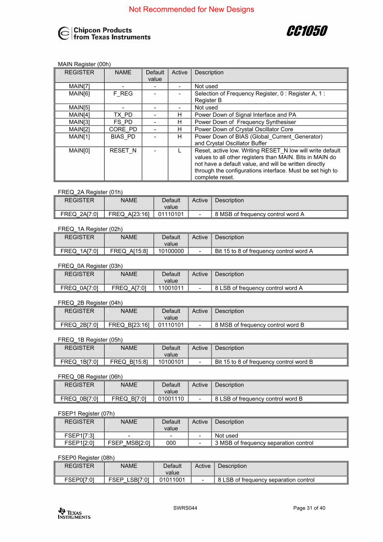
MAIN Register (00h) REGISTER NAME Default
value Active Description
MAIN[7] - - - Not used MAIN[6] F_REG - - Selection of Frequency Register, 0 : Register A, 1 :
Register B MAIN[5] - - - Not used MAIN[4] TX_PD - H Power Down of Signal Interface and PA MAIN[3] FS_PD - H Power Down of Frequency Synthesiser MAIN[2] CORE_PD - H Power Down of Crystal Oscillator Core MAIN[1] BIAS_PD - H Power Down of BIAS (Global_Current_Generator)
and Crystal Oscillator Buffer MAIN[0] RESET_N - L Reset, active low. Writing RESET_N low will write default
values to all other registers than MAIN. Bits in MAIN do not have a default value, and will be written directly through the configurations interface. Must be set high to complete reset.
FREQ_2A Register (01h)
REGISTER NAME Default value
Active Description
FREQ_2A[7:0] FREQ_A[23:16] 01110101 - 8 MSB of frequency control word A FREQ_1A Register (02h)
REGISTER NAME Default value
Active Description
FREQ_1A[7:0] FREQ_A[15:8] 10100000 - Bit 15 to 8 of frequency control word A FREQ_0A Register (03h)
REGISTER NAME Default value
Active Description
FREQ_0A[7:0] FREQ_A[7:0] 11001011 - 8 LSB of frequency control word A FREQ_2B Register (04h)
REGISTER NAME Default value
Active Description
FREQ_2B[7:0] FREQ_B[23:16] 01110101 - 8 MSB of frequency control word B FREQ_1B Register (05h)
REGISTER NAME Default value
Active Description
FREQ_1B[7:0] FREQ_B[15:8] 10100101 - Bit 15 to 8 of frequency control word B FREQ_0B Register (06h)
REGISTER NAME Default value
Active Description
FREQ_0B[7:0] FREQ_B[7:0] 01001110 - 8 LSB of frequency control word B FSEP1 Register (07h)
REGISTER NAME Default value
Active Description
FSEP1[7:3] - - - Not used FSEP1[2:0] FSEP_MSB[2:0] 000 - 3 MSB of frequency separation control
FSEP0 Register (08h)
REGISTER NAME Default value
Active Description
FSEP0[7:0] FSEP_LSB[7:0] 01011001 - 8 LSB of frequency separation control
Not Recommended for New Designs

CC1050
SWRS044 Page 32 of 40
CURRENT Register (09h) REGISTER NAME Default
value Active Description
CURRENT[7:4] VCO_CURRENT[3:0] 1100 - Control of current in VCO core 0000 : 160µA 0001 : 320µA 0010 : 480µA 0011 : 630µA 0100 : 790µA 0101 : 950µA 0110 : 1100µA 0111 : 1250µA 1000 : 1560µA, use for f< 500 MHz 1001 : 1720µA 1010 : 1870µA 1011 : 2030µA 1100 : 2180µA 1101 : 2340µA 1110 : 2490µA 1111 : 2640µA, use for f>500 MHz
CURRENT[3:2] - - Not used CURRENT[1:0] PA_DRIVE[1:0] 10 Control of current in VCO buffer for PA
00 : 1mA 01 : 2mA, use for TX, f<500 MHz 10 : 3mA 11 : 4mA, use for TX, f>500 MHz
XOSC Register (0Ah)
REGISTER NAME Default value
Active Description
XOSC[7:1] - - - Not used XOSC[0] XOSC_BYPASS 0 - 0 : Internal XOSC enabled
1 : Power-Down of XOSC, external CLK used
Not Recommended for New Designs

CC1050
SWRS044 Page 33 of 40
PA_POW Register (0Bh) REGISTER NAME Default
value Active Description
PA_POW[7:4] PA_HIGHPOWER[3:0] 0000 - Control of output power in high power array. Should be 0000 in PD mode . See Table 3 page 25 for details.
PA_POW[3:0] PA_LOWPOWER[3:0] 1111 - Control of output power in low power array Should be 0000 in PD mode. See Table 3 page 25 for details.
PLL Register (0Ch)
REGISTER NAME Default value
Active Description
PLL[7] EXT_FILTER 0 - 1 : External loop filter 0 : Internal loop filter 1-to-0 transition samples F_COMP comparator when BREAK_LOOP=1 (TEST3)
PLL[6:3] REFDIV[3:0] 0010 - Reference divider 0000 : Not allowed 0001 : Not allowed 0010 : Divide by 2 0011 : Divide by 3 ........... 1111 : Divide by 15
PLL[2] ALARM_DISABLE 0 h 0 : Alarm function enabled 1 : Alarm function disabled
PLL[1] ALARM_H - - Status bit for tuning voltage out of range (too close to VDD)
PLL[0] ALARM_L - - Status bit for tuning voltage out of range (too close to GND)
Not Recommended for New Designs

CC1050
SWRS044 Page 34 of 40
LOCK Register (0Dh) REGISTER NAME Default
value Active Description
LOCK[7:4] LOCK_SELECT[3:0] 0000 - Selection of signals to CHP_OUT (LOCK) pin 0000 : Normal, pin can be used as CHP_OUT 0001 : LOCK_CONTINUOUS (active high) 0010 : LOCK_INSTANT (active high) 0011 : ALARM_H (active high) 0100 : ALARM_L (active high) 0101 : CAL_COMPLETE (active high) 0110 : Not used 0111 : REFERENCE_DIVIDER Output 1000 : TX_PDB (active high, activates external PA when TX_PD=0) 1001 : Not used 1010 : Not used 1011 : Not used 1100 : Not used 1101 : Not used 1110 : N_DIVIDER Output 1111 : F_COMP
LOCK[3] PLL_LOCK_ ACCURACY
0 - 0 : Sets Lock Threshold = 127, Reset Lock Threshold = 111. Corresponds to a worst case accuracy of 0.7% 1 : Sets Lock Threshold = 31, Reset Lock Threshold =15. Corresponds to a worst case accuracy of 2.8%
LOCK[2] PLL_LOCK_ LENGTH
0 - 0 : Normal PLL lock window 1 : Not used
LOCK[1] LOCK_INSTANT - - Status bit from Lock Detector LOCK[0] LOCK_CONTINUOUS - - Status bit from Lock Detector
CAL Register (0Eh)
REGISTER NAME Default value
Active Description
CAL[7] CAL_START 0 ↑ ↑ 1 : Calibration started 0 : Calibration inactive CAL_START must be set to 0 after calibration is done
CAL[6] CAL_DUAL 0 H 1 : Store calibration in both A and B 0 : Store calibration in A or B defined by MAIN[6]
CAL[5] CAL_WAIT 0 H 1 : Normal Calibration Wait Time 0 : Half Calibration Wait Time The calibration time is proportional to the internal reference frequency. 2 MHz reference frequency gives 14 ms wait time.
CAL[4] CAL_CURRENT 0 H 1 : Calibration Current Doubled 0 : Normal Calibration Current
CAL[3] CAL_COMPLETE 0 H Status bit defining that calibration is complete
CAL[2:0] CAL_ITERATE 101 H Iteration start value for calibration DAC 000 - 101: Not used 110 : Normal start value 111 : Not used
Not Recommended for New Designs

CC1050
SWRS044 Page 35 of 40
MODEM0 Register (11h) REGISTER NAME Default
value Active Description
MODEM0[7] - - - Not used MODEM0[6:4] BAUDRATE[2:0] 010 - 000 : 0.6 kBaud
001 : 1.2 kBaud 010 : 2.4 kBaud 011 : 4.8 kBaud 100 : 9.6 kBaud 101 : 19.2 kBaud 110 : 38.4 kBaud 111 : 76.8 kBaud
MODEM0[3:2] DATA_FORMAT[1:0] 01 - 00 : NRZ operation. 01 : Manchester operation 10 : Transparent Asyncronous UART operation 11 : Not used
MODEM0[1:0] XOSC_FREQ[1:0] 00 - Selection of XTAL frequency range 00 : 3MHz - 4MHz crystal, 3.6864MHz recommended 01 : 6MHz - 8MHz crystal, 7.3728MHz recommended 10 : 9MHz - 12MHz crystal, 11.0592 MHz recommended 11 : 12MHz - 16MHz crystal, 14.7456MHz recommended
FSCTRL Register (13h)
REGISTER NAME Default value
Active Description
FSCTRL[7:4] - - - Not used FSCTRL[3:1] Reserved FSCTRL[0] FS_RESET_N 1 L Separate reset of frequency synthesizer
PRESCALER Register (1Ch)
REGISTER NAME Default value
Active Description
PRESCALER[7:6] PRE_SWING[1:0] 00 - Prescaler swing. Fractions for PRE_CURRENT[1:0] = 00 00 : 1 * Nominal Swing 01 : 2/3 * Nominal Swing 10 : 7/3 * Nominal Swing 11 : 5/3 * Nominal Swing
PRESCALER[5:4] PRE_CURRENT [1:0]
00 - Prescaler current scaling 00 : 1 * Nominal Current 01 : 2/3 * Nominal Current 10 : 1/2 * Nominal Current 11 : 2/5 * Nominal Current
PRESCALER[3] BYPASS_R 0 H Bypass the resistor in the PLL loop filter 0 : Not bypassed 1 : Bypassed
PRESCALER[2] DISCONNECT_C 0 - Disconnect the capacitor in the PLL loop filter 0 : Capacitor connected 1 : Capacitor disconnected. Use for data rate 38.4 and 76.8 kBaud only.
PRESCALER[1:0] - - - Not used
Not Recommended for New Designs

CC1050
SWRS044 Page 36 of 40
TEST6 Register (for test only, 40h) REGISTER NAME Default
value Active Description
TEST6[7] LOOPFILTER_TP1 0 - 1 : Select testpoint 1 to CHP_OUT 0 : CHP_OUT tied to GND
TEST6 [6] LOOPFILTER_TP2 0 - 1 : Select testpoint 2 to CHP_OUT 0 : CHP_OUT tied to GND
TEST6 [5] CHP_OVERRIDE 0 - 1 : use CHP_CO[4:0] value 0 : use calibrated value
TEST6[4:0] CHP_CO[4:0] 10000 - Charge_Pump Current DAC override value TEST5 Register (for test only, 41h)
REGISTER NAME Default value
Active Description
TEST5[7:6] - - - Not used TEST5[5] CHP_DISABLE 0 - 1 : CHP up and down pulses disabled
0 : normal operation TEST5[4] VCO_OVERRIDE 0 - 1 : use VCO_AO[3:0] value
0 : use calibrated value TEST5[3:0] VCO_AO[3:0] 1000 - VCO_ARRAY override value
TEST4 Register (for test only, 42h)
REGISTER NAME Default value
Active Description
TEST4[7:6] - - - Not used TEST4[5:0] L2KIO[5:0] 100101 h Constant setting charge pump current
scaling/rounding factor. Sets Bandwidth of PLL. Use 3Fh for 38.4 and 76.8 kBaud
TEST3 Register (for test only, 43h)
REGISTER NAME Default value
Active Description
TEST3[7:5] - - - Not used TEST3[4] BREAK_LOOP 0 - 1 : PLL loop open
0 : PLL loop closed TEST3[3:0] CAL_DAC_OPEN 0100 - Calibration DAC override value, active when
BREAK_LOOP =1 TEST2 Register (for test only, 44h)
REGISTER NAME Default value
Active Description
TEST2[7:5] - - - Not used TEST2[4:0] CHP_CURRENT
[4:0] - - Status vector defining applied
CHP_CURRENT value TEST1 Register (for test only, 45h)
REGISTER NAME Default value
Active Description
TEST1[7:4] - - - Not used TEST1[3:0] CAL_DAC[3:0] - - Status vector defining applied Calibration
DAC value TEST0 Register (for test only, 46h)
REGISTER NAME Default value
Active Description
TEST0[7:4] - - - Not used TEST0[3:0] VCO_ARRAY[3:0] - - Status vector defining applied VCO_ARRAY
value
Not Recommended for New Designs

CC1050
SWRS044 Page 37 of 40
Not Recommended for New Designs

CC1050
SWRS044 Page 38 of 40
Package Description (TSSOP-24)
Note: The figure is an illustration only.
Thin Shrink Small Outline Package (TSSOP) D E1 E A A1 E B L Copl. α TSSOP 24 Min
Max
7.7 7.9
4.30 4.50
6.40
1.20
0.05 0.15
0.65
0.19 0.30
0.45 0.75
0.10
0° 8°
All dimensions in mm Soldering Information Recommended soldering profile is according to IPC/JEDEC J-STD-020B, July 2002. Plastic Tube Specification TSSOP 4.4mm (.173”) antistatic tube.
Tube Specification Package Tube Width Tube Height Tube
Length Units per Tube
TSSOP 24 268 mil 80 mil 20” 62 Carrier Tape and Reel Specification Carrier tape and reel is in accordance with EIA Specification 481.
Tape and Reel Specification Package Tape Width Component
Pitch Hole Pitch
Reel Diameter
Units per Reel
TSSOP 24 16 mm 8 mm 4 mm 13” 2500
Not Recommended for New Designs

CC1050
SWRS044 Page 39 of 40
Ordering Information Ordering part number Description MOQ CC1050 Single Chip RF Transceiver 62 (tube) CC1050/T&R Single Chip RF Transceiver 2500 (tape and reel) CC1050DK-433 CC1050 Development Kit, 433 MHz 1 CC1050DK-868 CC1050 Development Kit, 868/915 MHz 1 CC1050SK CC1050 Sample Kit (5 pcs) 1
MOQ = Minimum Order Quantity General Information Document Revision History
Revision Date Description/Changes 1.1 April 2004 Shaping feature removed
L1 changed to 0603 size Crystal oscillator information added Preliminary version removed Minor corrections and editorial changes
1.2 August 2004 Application circuit and BOM simplified Description in the FSCTRL register changed KOA inductor removed in BOM Additional information on LC-filter
Disclaimer Chipcon AS believes the information contained herein is correct and accurate at the time of this printing. However, Chipcon AS reserves the right to make changes to this product without notice. Chipcon AS does not assume any responsibility for the use of the described product; neither does it convey any license under its patent rights, or the rights of others. The latest updates are available at the Chipcon website or by contacting Chipcon directly. To the extent possible, major changes of product specifications and functionality will be stated in product specific Errata Notes published at the Chipcon website. Customers are encouraged to sign up for the Developer’s Newsletter for the most recent updates on products and support tools. When a product is discontinued this will be done according to Chipcon’s procedure for obsolete products as described in Chipcon’s Quality Manual. This includes informing about last-time-buy options. The Quality Manual can be downloaded from Chipcon’s website. Trademarks SmartRF® is a registered trademark of Chipcon AS. SmartRF® is Chipcon's RF technology platform with RF library cells, modules and design expertise. Based on SmartRF® technology Chipcon develops standard component RF circuits as well as full custom ASICs based on customer requirements and this technology. All other trademarks, registered trademarks and product names are the sole property of their respective owners. Life Support Policy This Chipcon product is not designed for use in life support appliances, devices, or other systems where malfunction can reasonably be expected to result in significant personal injury to the user, or as a critical component in any life support device or system whose failure to perform can be reasonably expected to cause the failure of the life support device or system, or to affect its safety or effectiveness. Chipcon AS customers using or selling these products for use in such applications do so at their own risk and agree to fully indemnify Chipcon AS for any damages resulting from any improper use or sale. © 2004, Chipcon AS. All rights reserved.
Not Recommended for New Designs

IMPORTANT NOTICE
Texas Instruments Incorporated and its subsidiaries (TI) reserve the right to make corrections, enhancements, improvements and otherchanges to its semiconductor products and services per JESD46, latest issue, and to discontinue any product or service per JESD48, latestissue. Buyers should obtain the latest relevant information before placing orders and should verify that such information is current andcomplete. All semiconductor products (also referred to herein as “components”) are sold subject to TI’s terms and conditions of salesupplied at the time of order acknowledgment.
TI warrants performance of its components to the specifications applicable at the time of sale, in accordance with the warranty in TI’s termsand conditions of sale of semiconductor products. Testing and other quality control techniques are used to the extent TI deems necessaryto support this warranty. Except where mandated by applicable law, testing of all parameters of each component is not necessarilyperformed.
TI assumes no liability for applications assistance or the design of Buyers’ products. Buyers are responsible for their products andapplications using TI components. To minimize the risks associated with Buyers’ products and applications, Buyers should provideadequate design and operating safeguards.
TI does not warrant or represent that any license, either express or implied, is granted under any patent right, copyright, mask work right, orother intellectual property right relating to any combination, machine, or process in which TI components or services are used. Informationpublished by TI regarding third-party products or services does not constitute a license to use such products or services or a warranty orendorsement thereof. Use of such information may require a license from a third party under the patents or other intellectual property of thethird party, or a license from TI under the patents or other intellectual property of TI.
Reproduction of significant portions of TI information in TI data books or data sheets is permissible only if reproduction is without alterationand is accompanied by all associated warranties, conditions, limitations, and notices. TI is not responsible or liable for such altereddocumentation. Information of third parties may be subject to additional restrictions.
Resale of TI components or services with statements different from or beyond the parameters stated by TI for that component or servicevoids all express and any implied warranties for the associated TI component or service and is an unfair and deceptive business practice.TI is not responsible or liable for any such statements.
Buyer acknowledges and agrees that it is solely responsible for compliance with all legal, regulatory and safety-related requirementsconcerning its products, and any use of TI components in its applications, notwithstanding any applications-related information or supportthat may be provided by TI. Buyer represents and agrees that it has all the necessary expertise to create and implement safeguards whichanticipate dangerous consequences of failures, monitor failures and their consequences, lessen the likelihood of failures that might causeharm and take appropriate remedial actions. Buyer will fully indemnify TI and its representatives against any damages arising out of the useof any TI components in safety-critical applications.
In some cases, TI components may be promoted specifically to facilitate safety-related applications. With such components, TI’s goal is tohelp enable customers to design and create their own end-product solutions that meet applicable functional safety standards andrequirements. Nonetheless, such components are subject to these terms.
No TI components are authorized for use in FDA Class III (or similar life-critical medical equipment) unless authorized officers of the partieshave executed a special agreement specifically governing such use.
Only those TI components which TI has specifically designated as military grade or “enhanced plastic” are designed and intended for use inmilitary/aerospace applications or environments. Buyer acknowledges and agrees that any military or aerospace use of TI componentswhich have not been so designated is solely at the Buyer's risk, and that Buyer is solely responsible for compliance with all legal andregulatory requirements in connection with such use.
TI has specifically designated certain components as meeting ISO/TS16949 requirements, mainly for automotive use. In any case of use ofnon-designated products, TI will not be responsible for any failure to meet ISO/TS16949.
Products Applications
Audio www.ti.com/audio Automotive and Transportation www.ti.com/automotive
Amplifiers amplifier.ti.com Communications and Telecom www.ti.com/communications
Data Converters dataconverter.ti.com Computers and Peripherals www.ti.com/computers
DLP® Products www.dlp.com Consumer Electronics www.ti.com/consumer-apps
DSP dsp.ti.com Energy and Lighting www.ti.com/energy
Clocks and Timers www.ti.com/clocks Industrial www.ti.com/industrial
Interface interface.ti.com Medical www.ti.com/medical
Logic logic.ti.com Security www.ti.com/security
Power Mgmt power.ti.com Space, Avionics and Defense www.ti.com/space-avionics-defense
Microcontrollers microcontroller.ti.com Video and Imaging www.ti.com/video
RFID www.ti-rfid.com
OMAP Applications Processors www.ti.com/omap TI E2E Community e2e.ti.com
Wireless Connectivity www.ti.com/wirelessconnectivity
Mailing Address: Texas Instruments, Post Office Box 655303, Dallas, Texas 75265Copyright © 2013, Texas Instruments Incorporated