Simultaneous Four-Wave Mixing and Cross-Gain … · signal A and B are modulated separately with 60...
5
International Research Journal of Engineering and Technology (IRJET) e-ISSN: 2395-0056 Volume: 02 Issue: 06 | Sep-2015 www.irjet.net p-ISSN: 2395-0072 © 2015, IRJET ISO 9001:2008 Certified Journal Page 1291 Simultaneous Four-Wave Mixing and Cross-Gain Modulation for Implementing All Optical Full Adder without Assist Light Jaspreet Kaur 1 , Naveen Dhillon 2 , Rupinder Kaur 3 1 Lecturer, ECE, LPU, Punjab, India 2 HOD, ECE, RIET, Punjab, India 3 Assistant Professor, ECE, RIET, Punjab, India ---------------------------------------------------------------------***--------------------------------------------------------------------- Abstract – The ever increasing speed of telecommunication systems reaches the limit of electronic device and the demand for logic operations such as switching, decision-making, regenerating and basic or complex computing is rapidly increasing. Nowadays due to various advantages of optical networks like high speed, less complexity and compact size All-optical devices are preferred as compared to legacy networks. Optical gates are building blocks of these all-optical devices. Using non linearity of optical amplifiers it is possible to implement the optical logic gates. The implementation of all optical half adder is proposed in optical domain using SOA non linearity. Simultaneous four wave mixing and cross gain modulation in a Semiconductor optical amplifier are used to demonstrate all-optical full addition module of two NRZ on-off keying data streams using four semiconductor optical amplifiers and without the use of any assist light. In the experimental demonstration, we implement the logical functions with an extinction ratio larger than 15 dB and achieve error-free signal processing at the repetition rate of 60 Gbit/s. The output of AND gate is realized using FWM effect whereas NOR output is realized using XGM effect. The two outputs are combined using a coupler to obtain the final Full adder output at 60 Gbit/s. Key Words: Semiconductor optical amplifiers (SOA), Cross Gain Modulation (XGM), Four Wave Mixing (FWM), OEO (Optical to Electrical conversion). 1. INTRODUCTION Binary logic gates are the basic building blocks of all the digital circuits like adders, multiplexers, counters, decoders, registers etc [1].However in today’s scenario where the demand of high speed photonic networks is increasing continuously, the electronic gates are a major challenge because of the intermediate electrical processing involved. The increasing demand for high speed networks forced the modern research trends to ultra-fast all-optical signal processing. All-optical signal processing enhances speed and capacity of the optical networks by avoiding expensive and time consuming Optical to Electrical conversions and vice-versa. To overcome the speed limitations posed by these electrical signal processing, all optical networks have been anticipated as future of ultra high speed switching [1].The successful implementation of all optical networks will largely depend on use of optical logic gates, which will remove the conventional need of intermediate electrical signal processing. The optical logic gates are based on the principle of optical non-linearity which may be achieved by either using non linear fibre or wavelength conversions based on SOA[2][7]. As compared to fibre based non linearity, the use of SOA is highly appreciated because of many advantages linked with SOA, which include higher gain, wide bandwidth, and higher fidelity. 2. ALL-OPTICAL NETWORKS VS LEGACY NETWORKS The main purpose of using all-optical network was to keep the data signals completely in optical domain from transmitter to receiver to eliminate the electronic conversions. In case of optical to electrical to optical (OEO) systems, the incoming WDM fibre which consists of more than one wavelength is de-multiplexed into its constituent wavelengths [3]. Each wavelength requires a separate transponder which convert the optical signal into electrical, regenerate it and then again convert it into optical domain [3]. The signal is back converted into electrical domain for processing by electronic switch. These conversions lead to increase in complexity, cost and power consumption where in case of all-optical systems, transponders are needed only for the wavelengths that are dropped or added at a particular node [3]. With wavelength division multiplexing (WDM), different wavelengths could be multiplexed together in a single fibre. These wavelengths can also be amplified together, without using one amplifier per wavelength. Another benefit of the all-optical systems is the provisioning time for a new connection is greatly decreased, as equipment needs to be installed only at the endpoints, along the path [3].The use of all optical systems results in savings in
Transcript of Simultaneous Four-Wave Mixing and Cross-Gain … · signal A and B are modulated separately with 60...
International Research Journal of Engineering and Technology (IRJET) e-ISSN: 2395-0056
Volume: 02 Issue: 06 | Sep-2015 www.irjet.net p-ISSN: 2395-0072
© 2015, IRJET ISO 9001:2008 Certified Journal Page 1291
Simultaneous Four-Wave Mixing and Cross-Gain Modulation for
Implementing All Optical Full Adder without Assist Light
Jaspreet Kaur 1, Naveen Dhillon 2, Rupinder Kaur 3
1 Lecturer, ECE, LPU, Punjab, India 2 HOD, ECE, RIET, Punjab, India
3 Assistant Professor, ECE, RIET, Punjab, India
---------------------------------------------------------------------***---------------------------------------------------------------------
Abstract – The ever increasing speed of telecommunication systems reaches the limit of electronic device and the demand for logic operations such as switching, decision-making, regenerating and basic or complex computing is rapidly increasing. Nowadays due to various advantages of optical networks like high speed, less complexity and compact size All-optical devices are preferred as compared to legacy networks. Optical gates are building blocks of these all-optical devices. Using non linearity of optical amplifiers it is possible to implement the optical logic gates. The implementation of all optical half adder is proposed in optical domain using SOA non linearity. Simultaneous four wave mixing and cross gain modulation in a Semiconductor optical amplifier are used to demonstrate all-optical full addition module of two NRZ on-off keying data streams using four semiconductor optical amplifiers and without the use of any assist light. In the experimental demonstration, we implement the logical functions with an extinction ratio larger than 15 dB and achieve error-free signal processing at the repetition rate of 60 Gbit/s. The output of AND gate is realized using FWM effect whereas NOR output is realized using XGM effect. The two outputs are combined using a coupler to obtain the final Full adder output at 60 Gbit/s.
Key Words: Semiconductor optical amplifiers (SOA), Cross Gain Modulation (XGM), Four Wave Mixing (FWM), OEO (Optical to Electrical conversion).
1. INTRODUCTION Binary logic gates are the basic building blocks of all the digital circuits like adders, multiplexers, counters, decoders, registers etc [1].However in today’s scenario where the demand of high speed photonic networks is increasing continuously, the electronic gates are a major challenge because of the intermediate electrical processing involved. The increasing demand for high speed networks forced the modern research trends to ultra-fast all-optical signal processing. All-optical signal
processing enhances speed and capacity of the optical networks by avoiding expensive and time consuming Optical to Electrical conversions and vice-versa. To overcome the speed limitations posed by these electrical signal processing, all optical networks have been anticipated as future of ultra high speed switching [1].The successful implementation of all optical networks will largely depend on use of optical logic gates, which will remove the conventional need of intermediate electrical signal processing. The optical logic gates are based on the principle of optical non-linearity which may be achieved by either using non linear fibre or wavelength conversions based on SOA[2][7]. As compared to fibre based non linearity, the use of SOA is highly appreciated because of many advantages linked with SOA, which include higher gain, wide bandwidth, and higher fidelity.
2. ALL-OPTICAL NETWORKS VS LEGACY NETWORKS The main purpose of using all-optical network was to keep the data signals completely in optical domain from transmitter to receiver to eliminate the electronic conversions. In case of optical to electrical to optical (OEO) systems, the incoming WDM fibre which consists of more than one wavelength is de-multiplexed into its constituent wavelengths [3]. Each wavelength requires a separate transponder which convert the optical signal into electrical, regenerate it and then again convert it into optical domain [3]. The signal is back converted into electrical domain for processing by electronic switch. These conversions lead to increase in complexity, cost and power consumption where in case of all-optical systems, transponders are needed only for the wavelengths that are dropped or added at a particular node [3]. With wavelength division multiplexing (WDM), different wavelengths could be multiplexed together in a single fibre. These wavelengths can also be amplified together, without using one amplifier per wavelength. Another benefit of the all-optical systems is the provisioning time for a new connection is greatly decreased, as equipment needs to be installed only at the endpoints, along the path [3].The use of all optical systems results in savings in

International Research Journal of Engineering and Technology (IRJET) e-ISSN: 2395-0056
Volume: 02 Issue: 06 | Sep-2015 www.irjet.net p-ISSN: 2395-0072
© 2015, IRJET ISO 9001:2008 Certified Journal Page 1292
power consumption and leads to reduction in cost also and still it needs more advances to cope up with future networks [3]. So, all-optical arithmetic based devices are of great interest for research.
3. OPERATION PRINCIPLE The principle of an SOA is stimulated emission. When an input optical signal is fed to SOA it leads to stimulated emission on the excited electrons inside the SOA and as the input signal travels through the SOA, stimulated emission continues until the photons exit together as an amplified signal. Due to this the carrier density in the SOA changes, because the signal at one wavelength affects the gain of signal at another wavelength. This property of SOA can be used for implementation of high speed logic gates. Therefore, if two input signals with frequency difference less than 6nm and signal power to the pump power ratio nearly equal to 1 are given to SOA, the FWM effect and XGM effect can be observed simultaneously [4]. Hence, with this property of SOA we can extract AB or AB due to XGM effect from the system, when two input signals are fed at different power levels to SOA. Attenuators can be used for creating the difference in power of the input signals. With XGM effect, AB is obtained when A input is high and AB is obtained where as when B is high. On combining AB and AB, output of XOR gate is realized. The XOR gate results in the value of logic “1” when exactly one of the inputs equals to logic “1”. Also, due to the generation of harmonic frequency at sum and difference frequencies, FWM effect occurs which give output of AND operation i.e. AB, AND gate give output “1” when both the inputs are high as shown in figure 1.
A full-adder adds two one-bit binary numbers (A and B) and a carry in. This full-adder operation can be achieved by using two half adder. In first half adder input message signal A and B are modulated separately with 60 GB PRBS signal and coupled through a coupler which will give S AB. Now this signal is further modulated with Cin which can be expressed as X ABC By employing this principle, SOA can be used for implementation of logic gates. In full adder module, the outputs obtained from sum
and carry corresponding to the possible inputs are shown in table 1. Table 1: Truth table for full adder Input A Input B Input Cin Sum (Sout) Carry (cout)
0 0 0 0 0 0 0 1 1 0 0 1 0 1 0 0 1 1 0 1 1 0 0 1 0 1 0 1 0 1 1 1 0 0 1 1 1 1 1 1
4. EXPERIMENTAL DEMONSTRATION AND DISCUSSION The experimental setup for all-optical full adder has been shown in Figure 2. Two mode locked laser diodes (MLLD) produce two Gaussian pulses one at 1550 nm (Signal A) with power 13 dBm and other at 1553 nm (Signal B) at power 17dbm. The pulse trains are modulated by two intensity modulators with 60 Gbit/s PRBS data, separately. Then two branches are combined in the coupler for amplification. A power splitter is used to split the information signal into four branches.
In these four branches, four 2 nm band pass filters (BPF), two tuneable optical delay lines and four attenuators are used to extract the target data, align the time difference and control the powers. The information signals in the first two branches are coupled into SOA 1 after optimized polarization control. The average power of information signal A is attenuated to 1.29 dBm, while information signal B has the average power of 12.29 dBm, which is used as a pump signal. The property of XGM, which is insensitive to polarization, occurs with the high value of signal B and the function of AB is achieved, which is
International Research Journal of Engineering and Technology (IRJET) e-ISSN: 2395-0056
Volume: 02 Issue: 06 | Sep-2015 www.irjet.net p-ISSN: 2395-0072
© 2015, IRJET ISO 9001:2008 Certified Journal Page 1293
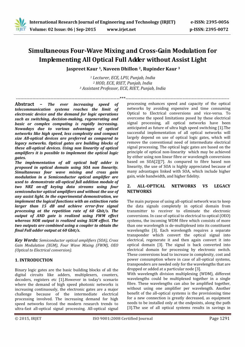
extracted by a 0.6 nm BPF centred at 1550 nm. Since the generation of FWM in the SOA is polarization dependent, the information signals in the other two branches are coupled into SOA 2 after the individual polarization control. The average powers of signal A and signal B are adjusted to 0.39 dBm and – 0.703 dBm, respectively. In this case, information signal A is used as a pump signal and the function of AB is filtered out by a 0.6 nm BPF at 1553 nm. Apart from this, a new signal is generated when both input signals are 1 i.e. AB, resulted from the FWM effect at 1547 nm (Harmonic frequency (FWM 2 B )) in SOA 2. The information signals AB and AB are combined to perform S AB. The average powers of AB, AB, AB and AB are 9.8 dBm, 10.3 dBm, -.092 dBm and 11.3dBm respectively. In this module, SOA 1 and SOA 2 are biased at 343 mA and 451 mA with 0.15 confinement factor. Now, the output of half adder is obtained at frequency 1550 nm and 1553 nm. So, frequency convertor is used at 1550 nm so as to achieve the output at single wavelength i.e at 1553 nm. This output S act as input for second half adder signal. The second output is obtained from carry in signal Cin at 1550 nm. These two input signals are divided into two parts by using a splitter. The information signals at different wavelength are combined through couplers. In first Coupler, the input Cin is at high power of 5.1 dBm where as input S is at low power of 1.1 dBm. In SOA 3, the output achieved by XGM is at 1553 nm. Similarly, in second Coupler, the input Cin is at low power of -0.77 dBm where as input S is at high power of 6.3 dBm. In SOA 4, the output achieved by XGM is at 1550 nm. On combining these outputs through coupler, output of full adder is achieved successfully. The output for carry out of full adder is obtained by combining the carry of two half adders. The outputs at different stages are as given below:
INPUT A = 1100001
INPUT B = 1011011
CARRY OF HALF ADDER (AB) = 1101000

International Research Journal of Engineering and Technology (IRJET) e-ISSN: 2395-0056
Volume: 02 Issue: 06 | Sep-2015 www.irjet.net p-ISSN: 2395-0072
© 2015, IRJET ISO 9001:2008 Certified Journal Page 1294
S = A B = 0100011
OUTPUT OF FULL ADDDER (S C) = 1111001
CARRY OUT COUT = 1101010
5. CONCLUSIONS The all-optical full adder has been implemented successfully with use of four SOAs. It consist of two signals A, B and a carry-in 60 Gbits/s NRZ-OOK signals as input and sum, carry-out as output . By the use of non-linear properties of SOA such as Cross Gain Modulation and Four Wave Mixing, logic operations such as XOR, AND, OR has been achieved. The BER Performance of all-optical full adder is approximately 10-5.
ACKNOWLEDGMENT We would like to thank our parents, friends and my Co Authors for being a constant source of inspiration and support while writing this research paper. Without their help this would not have been a success.
REFERENCES [1] Kristian E. Stubkjaer, “Semiconductor Optical Amplifier-Based All-Optical Gates for High-Speed Optical Processing”, IEEE Journal on selected topics in Quantum Electronics,Vol. 6, No. 6, November/December 2000 A. [2] A. Teixeira, T. Silveiral, P. Andrd, R Nogueiral, G. Tosi-Bellefi, P. Monteirol, J. Da Rochal, “All-optical switching with SOA based devices” 12- 17 September2005, Yaya, Cdmea, UkraIhe IEEE. [3] Adel A. M. Saleh and Jane M. Simmons, “All-Optical Networking – Evolution, Benefits, Challenges, and Future Vision”. Proceedings of the IEEE, vol. 100, no. 5, May 2012, pp. 1105-1117 © 2012 IEEE

International Research Journal of Engineering and Technology (IRJET) e-ISSN: 2395-0056
Volume: 02 Issue: 06 | Sep-2015 www.irjet.net p-ISSN: 2395-0072
© 2015, IRJET ISO 9001:2008 Certified Journal Page 1295
[4] Peili li, Xinliang Zhang, Zezhou Zheng and Dexiu Huang, “Simultaneous demonstration on 10 Gb/s wavelength conversion four-wave mixing and cross gain modulation in semiconductor optical amplifier” Opitca applicata, Vol XXXIV, No. 1,2004. [5] S. H. Kim, et al., “All-optical half adder using cross gain modulation in semiconductor optical amplifiers,” Opt. Express, vol. 14, no. 22, pp.10693–10698, 2006. [6] S. Kumar, A. E. Willner, D. Gurkan, K. R. Parameswaran, and M. M. Fejer, “All-optical half adder using an SOA and a PPLN waveguide for signal processing in optical networks,” Opt. Express, vol. 14, no. 22, pp. 10255–10260, 2006. [7] K. Sun, J. Qiu, M. Rochette, L. R. Chen,” All- Optical Logic Gates (XOR, AND, and OR) Based on Cross Phase Modulation in a Highly Nonlinear Fiber” ECOC 2009, 20-24 September, 2009, Vienna, Austria. [8] Bo Dai, Satoshi Shimizu, Xu Wang and Naoya Wada, “Simultaneous All-Optical Half-Adder and Half-Subtracter Based on Two Semiconductor Optical Amplifiers” ieee photonics technology letters, vol. 25, no. 1, january 1, 2013.


![Only General DescriptionUse - Digi-Key Sheets/Hittite Microwave PDFs... · Deterministic Jitter, Jd peak-to-peak, 215-1 PRBS input [1] 2 ps, p-p Propagation Delay, ... Timing Diagram](https://static.fdocuments.net/doc/165x107/5ac200307f8b9a213f8dbdd2/only-general-descriptionuse-digi-key-sheetshittite-microwave-pdfsdeterministic.jpg)