
Silicon Nanotechnology at Intel - Stmik...
26
Intel Nanotechnology Virtual Open House 1 Silicon Nanotechnology at Intel Ken David Ken David Director of Components Research Director of Components Research Technology and Manufacturing Group Technology and Manufacturing Group Intel Corporation Intel Corporation October 22, 2004 October 22, 2004
Transcript of Silicon Nanotechnology at Intel - Stmik...
Intel Nanotechnology Virtual Open House
1
Silicon Nanotechnologyat Intel
Ken DavidKen DavidDirector of Components ResearchDirector of Components Research
Technology and Manufacturing GroupTechnology and Manufacturing GroupIntel CorporationIntel CorporationOctober 22, 2004October 22, 2004
Intel Nanotechnology Virtual Open House 2
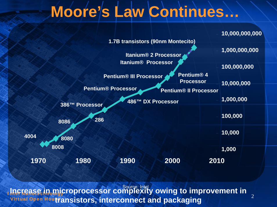
Moore’s Law Continues…
Increase in microprocessor complexity owing to improvement in transistors, interconnect and packaging
4004 8080
8086
8008
Pentium® Processor
486™ DX Processor386™ Processor
286
Pentium® II Processor
Pentium® III Processor
Itanium® Processor
Pentium® 4 Processor
Itanium® 2 Processor
1,000
10,000
100,000
1,000,000
10,000,000
100,000,000
1,000,000,000
10,000,000,000
1970 1980 1990 2000 2010
Source: Intel
1.7B transistors (90nm Montecito)
Intel Nanotechnology Virtual Open House 3
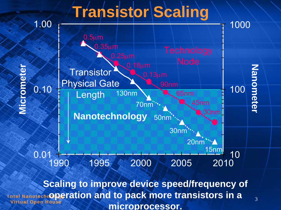
TechnologyNode
0.5µm0.35µm
0.25µm0.18µm
0.13µm90nm
65nm45nm
30nm
TransistorPhysical Gate
Length 130nm70nm
50nm
30nm20nm
15nm
1995 20051990 2000 20100.01
0.10
1.00M
icro
met
er
Nanotechnology
10
100
1000N
anometer
Transistor Scaling
Scaling to improve device speed/frequency of operation and to pack more transistors in a
microprocessor.
Intel Nanotechnology Virtual Open House 4
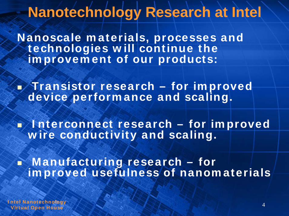
Nanotechnology Research at IntelNanoscale materials, processes and
technologies will continue the improvement of our products:
Transistor research – for improved device performance and scaling.
Interconnect research – for improved wire conductivity and scaling.
Manufacturing research – for improved usefulness of nanomaterials
Intel Nanotechnology Virtual Open House 5
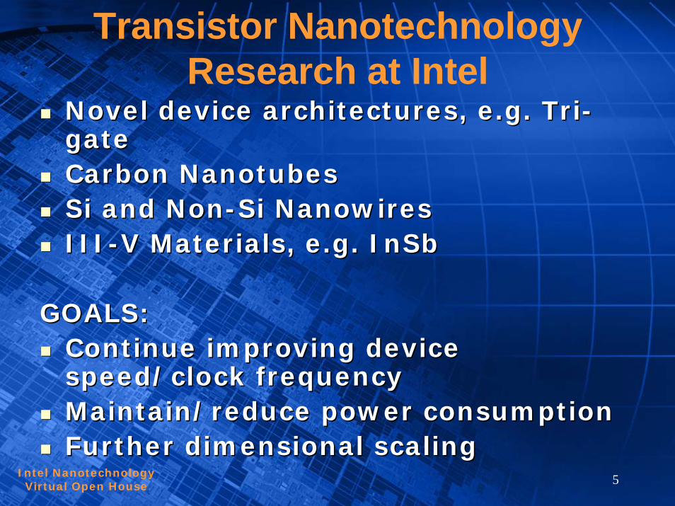
Transistor Nanotechnology Research at Intel
Novel device architectures, e.g. TriNovel device architectures, e.g. Tri--gategateCarbon Carbon NanotubesNanotubesSiSi and Nonand Non--SiSi NanowiresNanowiresIIIIII--V Materials, e.g. V Materials, e.g. InSbInSb
GOALS: GOALS: Continue improving device Continue improving device speed/clock frequencyspeed/clock frequencyMaintain/reduce power consumptionMaintain/reduce power consumptionFurther dimensional scalingFurther dimensional scaling
Intel Nanotechnology Virtual Open House 6
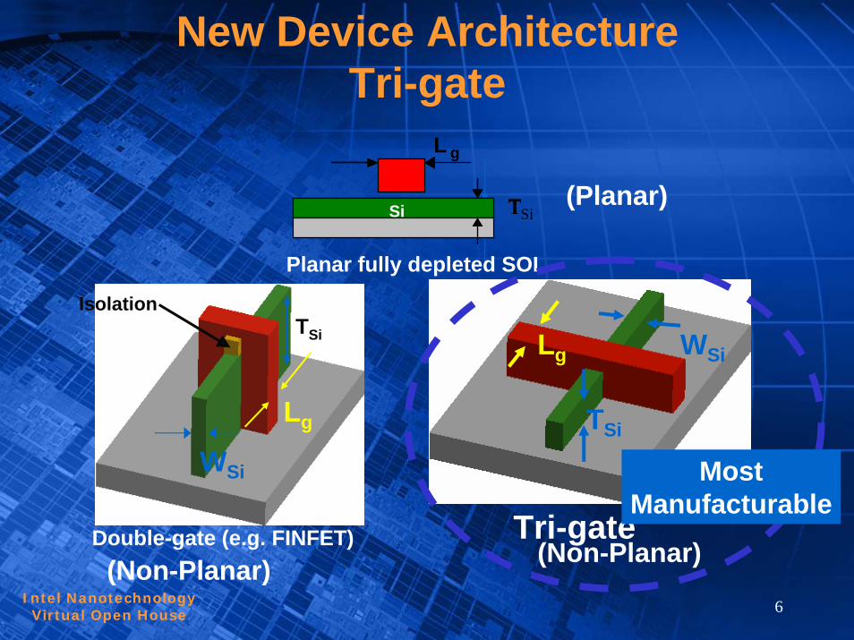
New Device ArchitectureTri-gate
Si TSi
L g
Si T
Planar fully depleted SOI
Double-gate (e.g. FINFET)
WSi
Lg
TSi
Isolation
(Non-Planar)
(Planar)
WSiLg
TSi
Tri-gate (Non-Planar)
MostManufacturable
Intel Nanotechnology Virtual Open House 7
Nano-Device Structure Evolution
Tri-gate Transistor
Gate
Fully-Surround Gate Transistor
Best Electrostatics and Scalability
Improved Electrostatics
SiO
2
Gate
SiO
2
Improving electrostatics optimizes power consumption and performance
Conventional Planar Transistor
Intel Nanotechnology Virtual Open House 8
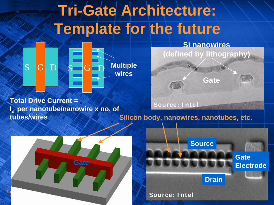
Tri-Gate Architecture:Template for the future
Gate
Si nanowires(defined by lithography)
Gate
Silicon body, nanowires, nanotubes, etc.
S DG Multiplewires
Total Drive Current = Id per nanotube/nanowire x no. of tubes/wires
S DG
GateElectrode
Source
Drain
Source: Intel
Source: Intel
Intel Nanotechnology Virtual Open House 9
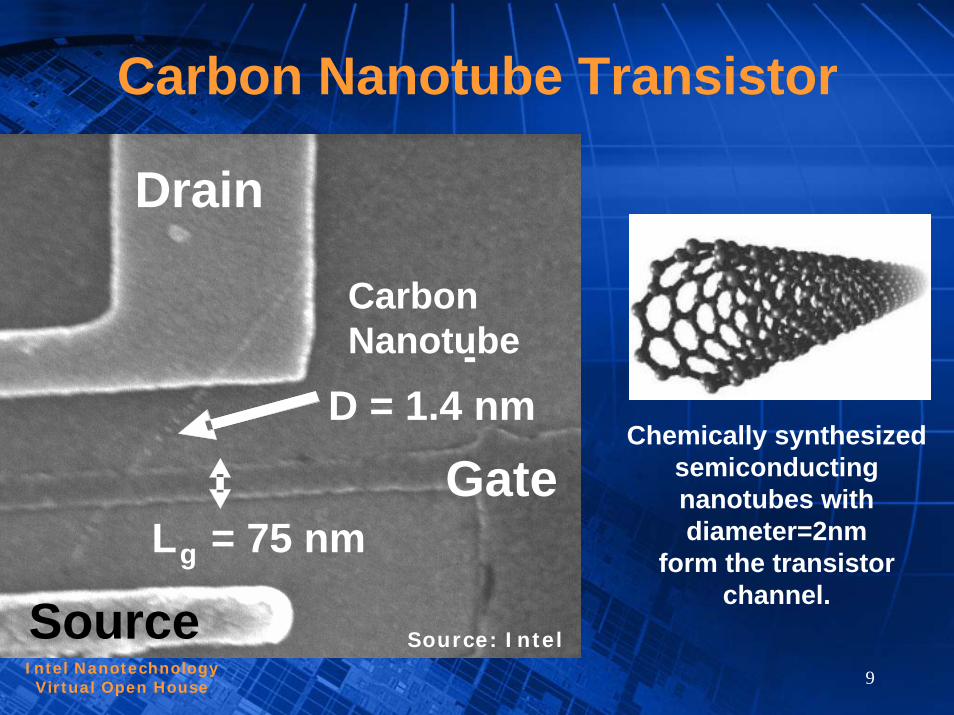
Carbon Nanotube Transistor
Source
CarbonNanotube-
D = 1.4 nm
Gate
Drain
Lg = 75 nm
Chemically synthesized semiconductingnanotubes with diameter=2nm
form the transistor channel.
Source: Intel
Intel Nanotechnology Virtual Open House 10
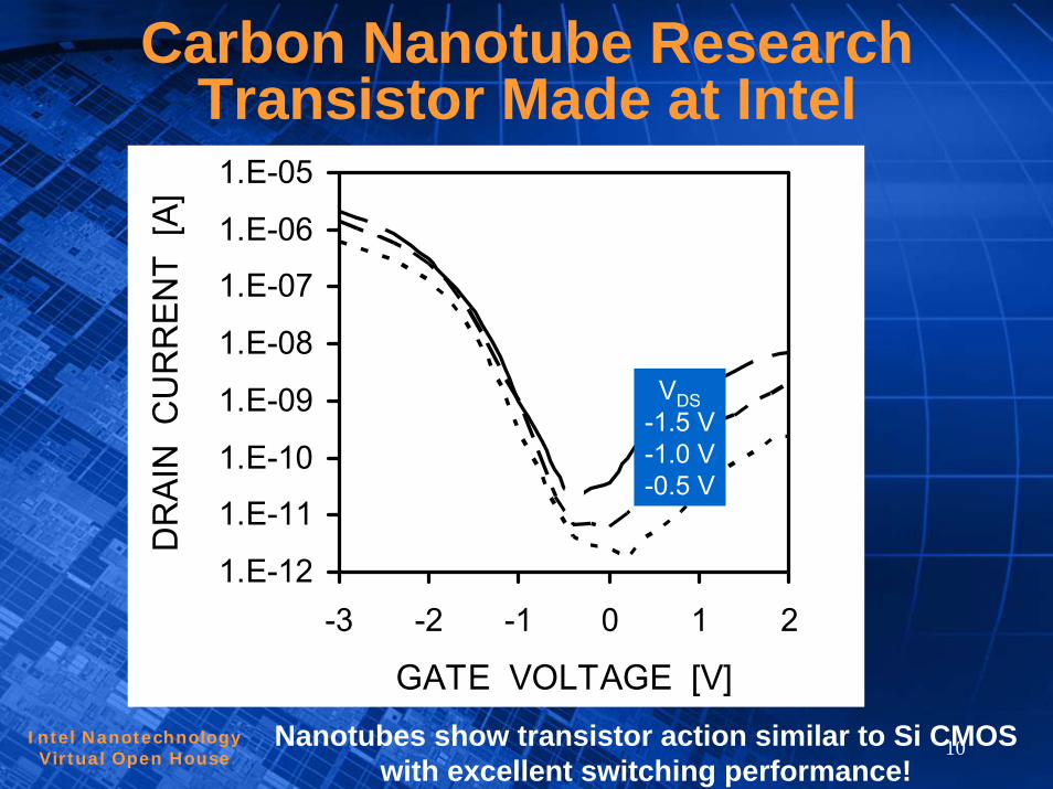
Carbon Nanotube Research Transistor Made at Intel
1.E-12
1.E-11
1.E-10
1.E-09
1.E-08
1.E-07
1.E-06
1.E-05
-3 -2 -1 0 1 2
GATE VOLTAGE [V]
DR
AIN
CU
RR
ENT
[A]
VDS-1.5 V-1.0 V-0.5 V
Carbon nanotubeP-ch Transistor
Nanotubes show transistor action similar to Si CMOS with excellent switching performance!
Intel Nanotechnology Virtual Open House 11
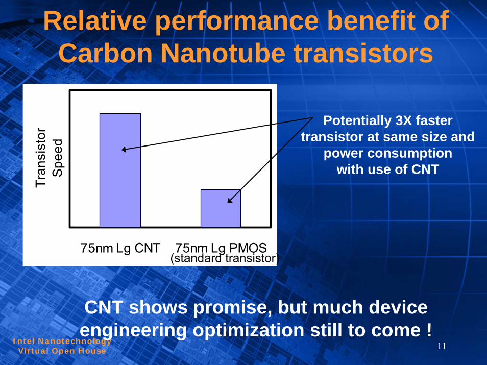
Relative performance benefit of Carbon Nanotube transistors
Potentially 3X faster transistor at same size and
power consumptionwith use of CNT
75nm Lg CNT 75nm Lg PMOS
Tran
sist
orS
peed
(standard transistor)
CNT shows promise, but much device engineering optimization still to come !
Intel Nanotechnology Virtual Open House 12
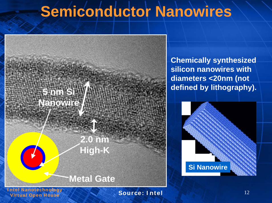
Semiconductor Nanowires
5 nm SiNanowire
Metal Gate
2.0 nm High-K
Chemically synthesized silicon nanowires with diameters <20nm (not defined by lithography).
Si Nanowire
Source: Intel
Intel Nanotechnology Virtual Open House 13
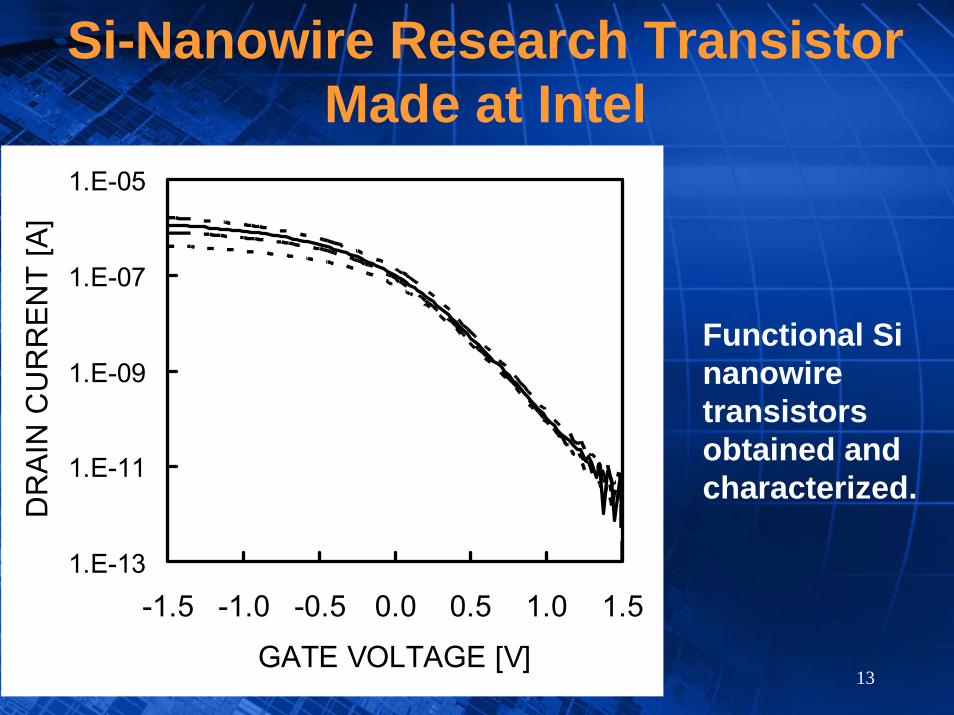
Si-Nanowire Research Transistor Made at Intel
1.E-13
1.E-11
1.E-09
1.E-07
1.E-05
-1.5 -1.0 -0.5 0.0 0.5 1.0 1.5
GATE VOLTAGE [V]
DR
AIN
CU
RR
EN
T [A
]
Si-NanowireP-ch Transistor
VDS = -0.25 to -1VStep: -0.25V
Functional Sinanowiretransistors obtained and characterized.
Intel Nanotechnology Virtual Open House 14
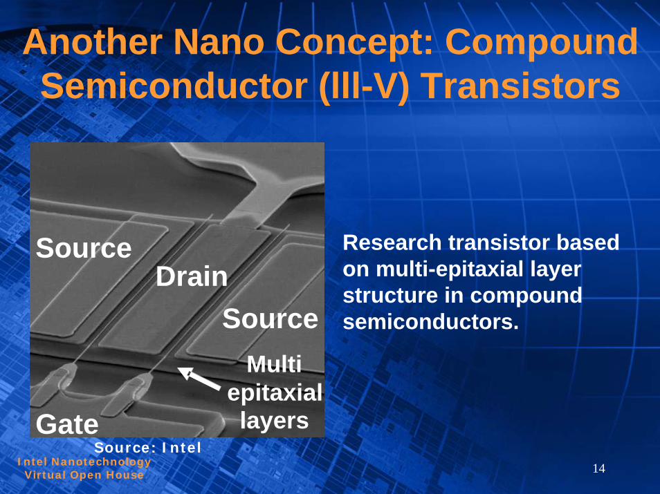
Another Nano Concept: Compound Semiconductor (lll-V) Transistors
Gate
DrainSource
SourceMulti
epitaxiallayers
Research transistor based on multi-epitaxial layer structure in compound semiconductors.
Source: Intel
Intel Nanotechnology Virtual Open House 15
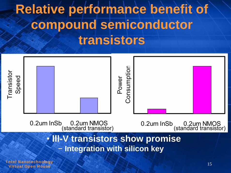
Relative performance benefit of compound semiconductor
transistors
0.2um InSb 0.2um NMOSPo
wer
Con
sum
ptio
n0.2um InSb 0.2um NMOS
Tran
sist
orS
peed
(standard transistor) (standard transistor)
• lll-V transistors show promise− Integration with silicon key
Intel Nanotechnology Virtual Open House
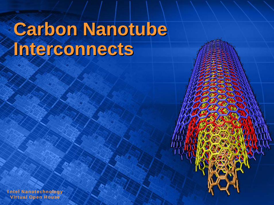
Carbon Nanotube Carbon Nanotube InterconnectsInterconnects
Intel Nanotechnology Virtual Open House 17
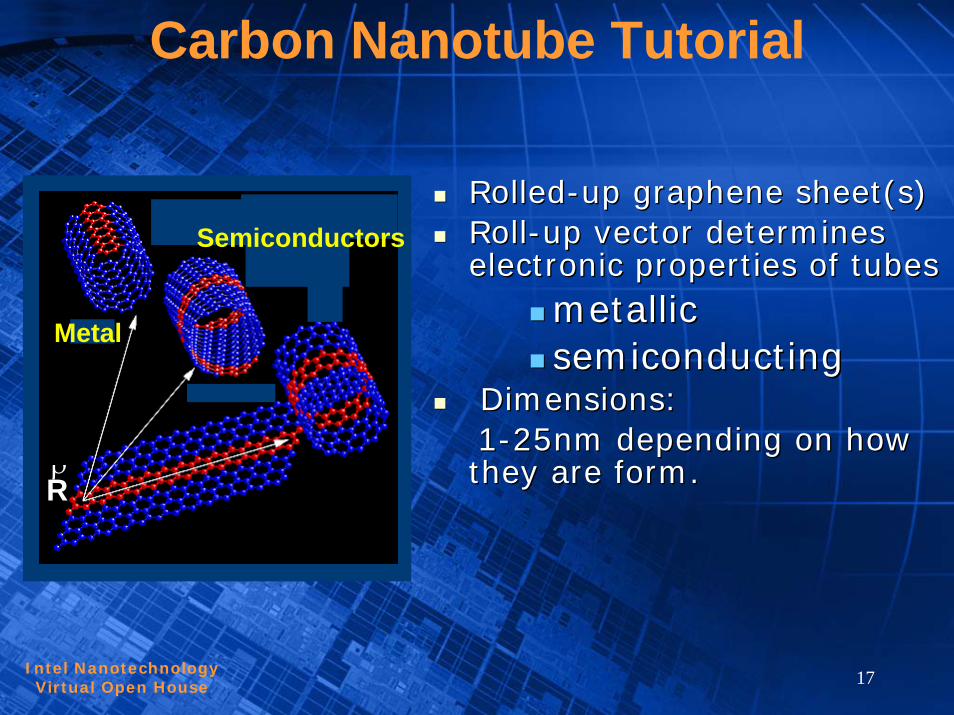
Carbon Nanotube Tutorial
RolledRolled--up graphene sheet(s)up graphene sheet(s)RollRoll--up vector determines up vector determines electronic properties of tubes electronic properties of tubes
metallic metallic semiconductingsemiconducting
Dimensions:Dimensions:11--25nm depending on how 25nm depending on how they are form.they are form.
Semi-conductor
Metal
Rρ
Semiconductors
Intel Nanotechnology Virtual Open House 18
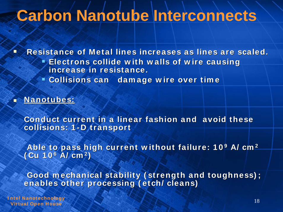
Carbon Nanotube Interconnects
Resistance of Metal lines increases as lines are scaled. Resistance of Metal lines increases as lines are scaled. Electrons collide with walls of wire causing Electrons collide with walls of wire causing increase in resistance.increase in resistance.Collisions can damage wire over timeCollisions can damage wire over time
NanotubesNanotubes::
Conduct current in a linear fashion and avoid these Conduct current in a linear fashion and avoid these collisions: 1collisions: 1--D transportD transport
Able to pass high current without failure: 10Able to pass high current without failure: 1099 A/cmA/cm22
(Cu 10(Cu 1066 A/cmA/cm22))
Good mechanical stability (strength and toughness); Good mechanical stability (strength and toughness); enables other processing (etch/cleans)enables other processing (etch/cleans)
Intel Nanotechnology Virtual Open House 19
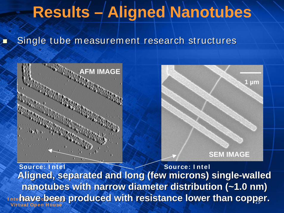
Results – Aligned NanotubesSingle tube measurement research structuresSingle tube measurement research structures
SEM IMAGE
AFM IMAGE
Aligned, separated and long (few microns) singleAligned, separated and long (few microns) single--walled walled nanotubesnanotubes with narrow diameter distribution (~1.0 nm) with narrow diameter distribution (~1.0 nm) have been produced with resistance lower than copper.have been produced with resistance lower than copper.
1 µm
Source: Intel Source: Intel
Intel Nanotechnology Virtual Open House 20
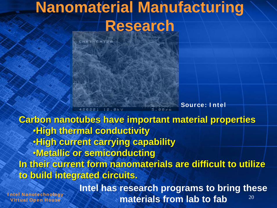
Nanomaterial Manufacturing Research
Carbon nanotubes have important material propertiesCarbon nanotubes have important material properties••High thermal conductivityHigh thermal conductivity••High current carrying capabilityHigh current carrying capability••Metallic or Metallic or semiconductingsemiconducting
In their current form In their current form nanomaterialsnanomaterials are difficult to utilize are difficult to utilize to build integrated circuits.to build integrated circuits.
Intel has research programs to bring these materials from lab to fab
Source: Intel
Intel Nanotechnology Virtual Open House 21
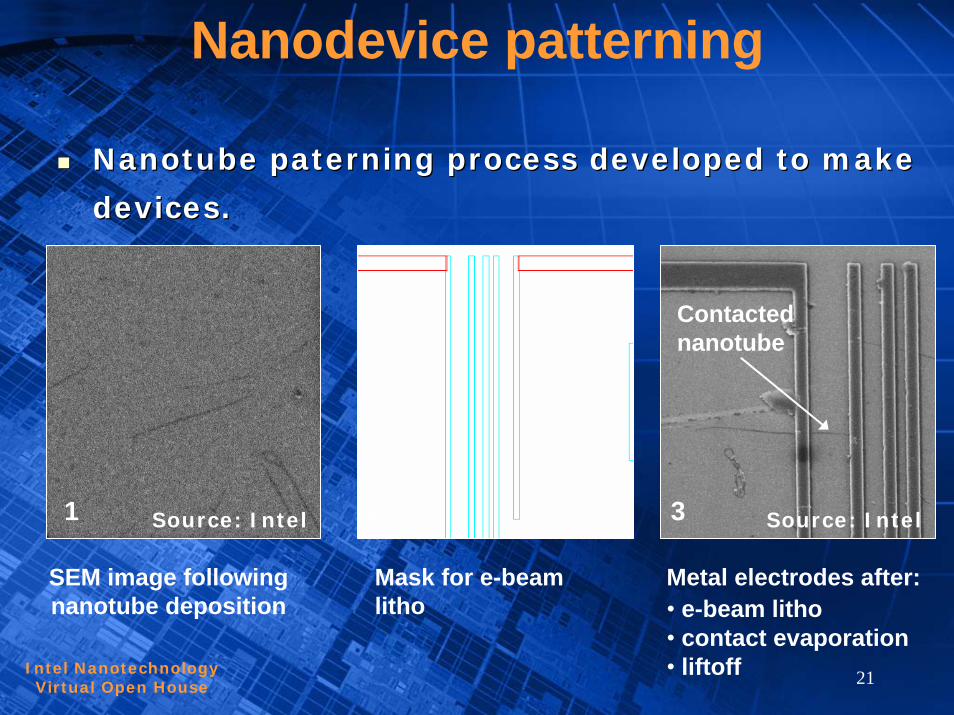
Nanodevice patterning
NanotubeNanotube paterningpaterning process developed to make process developed to make
devices.devices.
SEM image following nanotube deposition
Mask for e-beam litho
Metal electrodes after:• e-beam litho• contact evaporation• liftoff
1 2 3
Contacted nanotube
Source: Intel Source: Intel
Intel Nanotechnology Virtual Open House 22
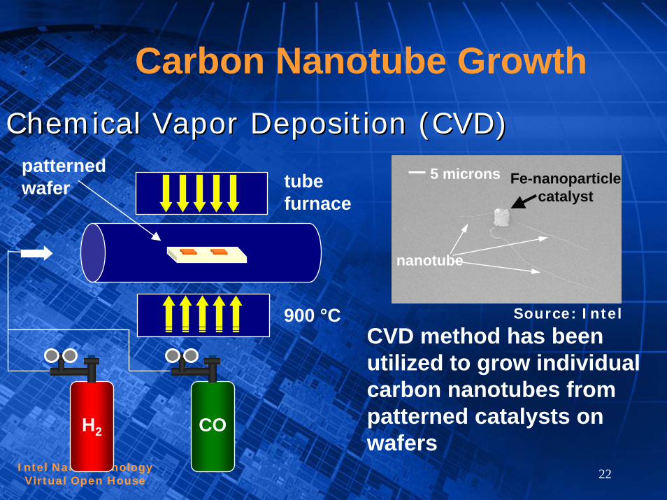
Carbon Nanotube GrowthChemical Vapor Deposition (CVD)Chemical Vapor Deposition (CVD)
H2 CO
patterned wafer
5 microns
nanotube
Fe-nanoparticle catalyst
tube furnace
900 °C Source: Intel
CVD method has been utilized to grow individual carbon nanotubes from patterned catalysts on wafers
Intel Nanotechnology Virtual Open House 23
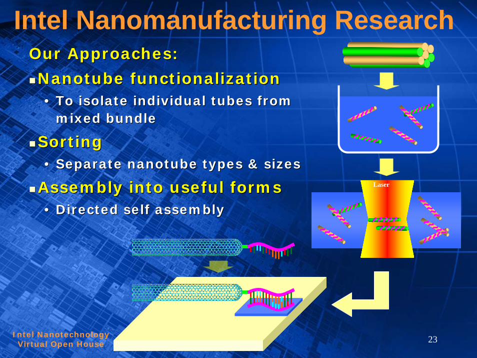
Intel Nanomanufacturing ResearchOur Approaches:Our Approaches:
Nanotube functionalizationNanotube functionalization•• To isolate individual tubes from To isolate individual tubes from
mixed bundlemixed bundle
SortingSorting•• Separate nanotube types & sizesSeparate nanotube types & sizes
Assembly into useful formsAssembly into useful forms•• Directed self assemblyDirected self assembly
Laser
Intel Nanotechnology Virtual Open House 24
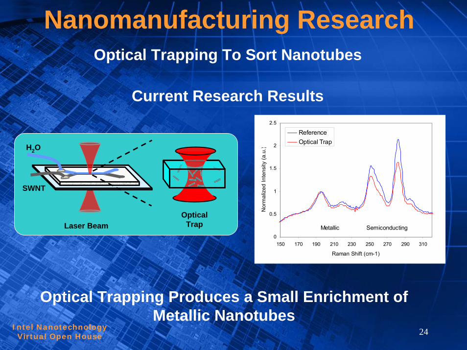
Nanomanufacturing ResearchOptical Trapping To Sort Nanotubes
Current Research Results
H2O
SWNT
Laser BeamOptical
Trap0
0.5
1
1.5
2
2.5
150 170 190 210 230 250 270 290 310
Raman Shift (cm-1)
Nor
mal
ized
Inte
nsity
(a.u
.)
ReferenceOptical Trap
Metallic Semiconducting
Optical Trapping Produces a Small Enrichment of Metallic Nanotubes
Intel Nanotechnology Virtual Open House 25
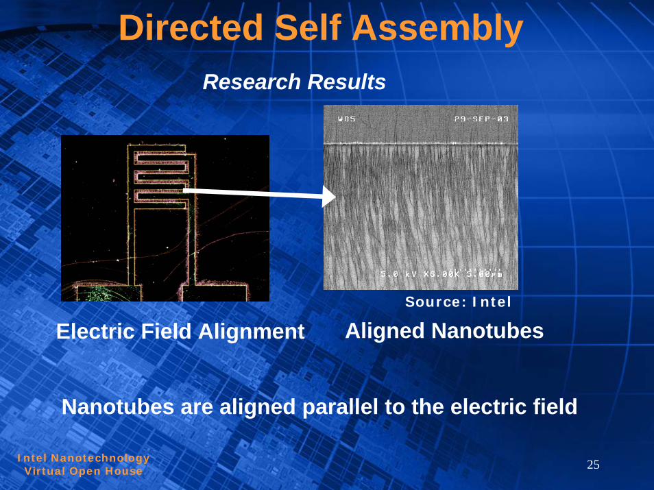
Directed Self Assembly
Nanotubes are aligned parallel to the electric field
Research Results
Aligned NanotubesElectric Field AlignmentSource: Intel
Intel Nanotechnology Virtual Open House 26
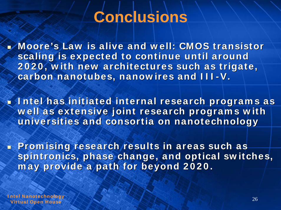
Conclusions
MooreMoore’’s Law is alive and well: CMOS transistor s Law is alive and well: CMOS transistor scaling is expected to continue until around scaling is expected to continue until around 2020, with new architectures such as 2020, with new architectures such as trigatetrigate, , carbon carbon nanotubesnanotubes, , nanowiresnanowires and IIIand III--V.V.
Intel has initiated internal research programs as Intel has initiated internal research programs as well as extensive joint research programs with well as extensive joint research programs with universities and consortia on nanotechnologyuniversities and consortia on nanotechnology
Promising research results in areas such as Promising research results in areas such as spintronicsspintronics, phase change, and optical switches, , phase change, and optical switches, may provide a path for beyond 2020. may provide a path for beyond 2020.


![Silicon Etch Process Options for Micro- and Nanotechnology using Inductively Coupled Plasmas References [1] See //.](https://static.fdocuments.net/doc/165x107/56649dc85503460f94abd9ac/silicon-etch-process-options-for-micro-and-nanotechnology-using-inductively.jpg)


