Silicon nanostructures for photonics and photovoltaics -...
14
NATURE NANOTECHNOLOGY | VOL 9 | JANUARY 2014 | www.nature.com/naturenanotechnology 19 C rystalline silicon (c-Si) is the most important semiconduc- tor material for the electronics and photovoltaics industries today, and it has become the cornerstone of our knowledge- based society. is prominent position follows from a unique com- bination of advantageous properties: the availability of large single crystals, high purity, effective conductivity engineering, a matching insulator and, very importantly, natural abundance. ese proper- ties have enabled the electronics industry to follow Moore’s law for over four decades, which is truly remarkable and which has driven the development of silicon technology to its present maturity. Together with its 1.1-eV bandgap — optimal for capturing the solar spectrum using a single-junction device — this maturity makes sili- con almost ideally suited for photovoltaics applications. As a result, around 90% of solar panels in use today are based on silicon. e optical properties of c-Si are relatively poor, owing to its indi- rect bandgap which precludes the efficient emission and absorption of light. is is a considerable weakness, especially given that some properties of c-Si are already very good, as illustrated, for example, by the successful realization of Raman lasing 1–4 and the demonstra- tion of ultrafast electro-optic modulation 5,6 . High performance in all aspects of optical functionality is highly desired, as it would enable true optoelectronic integration and pave the way to faster, highly integrated and low-cost devices. For photovoltaics applications, higher optoelectronic performance would be the much-desired ena- bler of a new generation of high-efficiency thin-film Si solar cells. We believe that nanostructures offer a range of opportunities for all of these application areas and that nanostructures herald a new era of silicon photonics and photovoltaics. Silicon nanostructures for communications Optical signals are now well established as a means for efficient data transfer from very long (Internet) to very short (rack-to-rack) distances. On-chip data processing is still being performed elec- tronically, however, even though processor clock speeds have been limited by the interconnect problem for a number of years 7 . e next step-change is to introduce photonics into on-chip commu- nications, which requires nanoscale optical sources, circuits and detectors to encode and transmit data around the chip. Silicon is Silicon nanostructures for photonics and photovoltaics Francesco Priolo 1,2,3 *, Tom Gregorkiewicz 4 , Matteo Galli 5 and Thomas F. Krauss 6 Silicon has long been established as the material of choice for the microelectronics industry. This is not yet true in photonics, where the limited degrees of freedom in material design combined with the indirect bandgap are a major constraint. Recent developments, especially those enabled by nanoscale engineering of the electronic and photonic properties, are starting to change the picture, and some silicon nanostructures now approach or even exceed the performance of equivalent direct-band- gap materials. Focusing on two application areas, namely communications and photovoltaics, we review recent progress in silicon nanocrystals, nanowires and photonic crystals as key examples of functional nanostructures. We assess the state of the art in each field and highlight the challenges that need to be overcome to make silicon a truly high-performing photonic material. poised to deliver this functionality, as silicon photonic devices are CMOS-compatible, and many highly performing devices have already been demonstrated 1–12 . Photonic crystal nanostructures add unique capabilities to this toolkit, as they offer extremely tight light confinement, thus providing strongly enhanced nonlinear effects already for microwatt pump power levels 8,9 , modulators with very low (femtojoule per bit level) switching energy 10,11 and the opportu- nity for enhancing and suppressing spontaneous emission 12 . In addition to nanostructuring, many material engineering options have been explored, such as the alloying of silicon and ger- manium 13 , doping 14,15 , strain and defect engineering 16,17 . Arguably the most successful way to manipulate the energy structure of Si, however, is to use quantum confinement in nanostructures 18 . Semiconductor nanostructures — nanocrystals and nanowires — are widely investigated in view of their exciting physical properties and with an eye to possible optoelectronic, photonic and pho- tovoltaic applications. In particular, owing to the modification of the energy structure afforded by quantization, semiconductor nanocrystals emerge as ideal candidates for photonic applications involving efficient radiative recombination. e best examples high- lighting the advantages of quantization of direct-bandgap semicon- ductors are quantum dots 19,20 , with quantization in silicon offering similar benefits, as we will explore next. Nanocrystals and nanowires. Silicon nanocrystals have been stud- ied intensively over the past decade 21,22 . Most notably, it has been established that the excitonic emission from Si nanocrystals has two characteristic features: with decreasing crystal size, the spectrum shiſts to the blue and its intensity increases. is observation indicates the quantization-related increase of the bandgap and the enhance- ment of the radiative recombination rate, as momentum conser- vation is gradually relaxed with reducing grain size owing to the Heisenberg principle 23 , while the transition itself remains indirect. Further, a possible participation of oxygen and/or interface-related states has been suggested that leads to a stabilization of the photo- luminescence wavelength for Si nanocrystals smaller than 3 nm in diameter 24–26 . See Box 1 for a review of the fabrication methods and Box 2 for a summary of the properties of Si nanocrystals. 1 Scuola Superiore di Catania, Università di Catania, via Valdisavoia 9, 95123 Catania, Italy, 2 Dipartimento di Fisica e Astronomia, Università di Catania, via S. Sofia 64, 95123 Catania, Italy, 3 MATIS IMM-CNR, via S. Sofia 64, 95123 Catania, Italy, 4 Van der Waals-Zeeman Institute, University of Amsterdam, Science Park 904, 1098 XH Amsterdam, The Netherlands, 5 Dipartimento di Fisica, Università di Pavia, via Bassi 6, 27100 Pavia, Italy, 6 Department of Physics, University of York, York YO10 5DD, UK. *e-mail: [email protected] REVIEW ARTICLE PUBLISHED ONLINE: 6 JANUARY 2014 | DOI: 10.1038/NNANO.2014.271 © 2014 Macmillan Publishers Limited. All rights reserved
Transcript of Silicon nanostructures for photonics and photovoltaics -...
NATURE NANOTECHNOLOGY | VOL 9 | JANUARY 2014 | www.nature.com/naturenanotechnology 19
Crystalline silicon (c-Si) is the most important semiconduc-tor material for the electronics and photovoltaics industries today, and it has become the cornerstone of our knowledge-
based society. This prominent position follows from a unique com-bination of advantageous properties: the availability of large single crystals, high purity, effective conductivity engineering, a matching insulator and, very importantly, natural abundance. These proper-ties have enabled the electronics industry to follow Moore’s law for over four decades, which is truly remarkable and which has driven the development of silicon technology to its present maturity. Together with its 1.1-eV bandgap — optimal for capturing the solar spectrum using a single-junction device — this maturity makes sili-con almost ideally suited for photovoltaics applications. As a result, around 90% of solar panels in use today are based on silicon.
The optical properties of c-Si are relatively poor, owing to its indi-rect bandgap which precludes the efficient emission and absorption of light. This is a considerable weakness, especially given that some properties of c-Si are already very good, as illustrated, for example, by the successful realization of Raman lasing1–4 and the demonstra-tion of ultrafast electro-optic modulation5,6. High performance in all aspects of optical functionality is highly desired, as it would enable true optoelectronic integration and pave the way to faster, highly integrated and low-cost devices. For photovoltaics applications, higher optoelectronic performance would be the much-desired ena-bler of a new generation of high-efficiency thin-film Si solar cells. We believe that nanostructures offer a range of opportunities for all of these application areas and that nanostructures herald a new era of silicon photonics and photovoltaics.
Silicon nanostructures for communicationsOptical signals are now well established as a means for efficient data transfer from very long (Internet) to very short (rack-to-rack) distances. On-chip data processing is still being performed elec-tronically, however, even though processor clock speeds have been limited by the interconnect problem for a number of years7. The next step-change is to introduce photonics into on-chip commu-nications, which requires nanoscale optical sources, circuits and detectors to encode and transmit data around the chip. Silicon is
Silicon nanostructures for photonics and photovoltaicsFrancesco Priolo1,2,3*, Tom Gregorkiewicz4, Matteo Galli5 and Thomas F. Krauss6
Silicon has long been established as the material of choice for the microelectronics industry. This is not yet true in photonics, where the limited degrees of freedom in material design combined with the indirect bandgap are a major constraint. Recent developments, especially those enabled by nanoscale engineering of the electronic and photonic properties, are starting to change the picture, and some silicon nanostructures now approach or even exceed the performance of equivalent direct-band-gap materials. Focusing on two application areas, namely communications and photovoltaics, we review recent progress in silicon nanocrystals, nanowires and photonic crystals as key examples of functional nanostructures. We assess the state of the art in each field and highlight the challenges that need to be overcome to make silicon a truly high-performing photonic material.
poised to deliver this functionality, as silicon photonic devices are CMOS-compatible, and many highly performing devices have already been demonstrated1–12. Photonic crystal nanostructures add unique capabilities to this toolkit, as they offer extremely tight light confinement, thus providing strongly enhanced nonlinear effects already for microwatt pump power levels8,9, modulators with very low (femtojoule per bit level) switching energy10,11 and the opportu-nity for enhancing and suppressing spontaneous emission12.
In addition to nanostructuring, many material engineering options have been explored, such as the alloying of silicon and ger-manium13, doping14,15, strain and defect engineering16,17. Arguably the most successful way to manipulate the energy structure of Si, however, is to use quantum confinement in nanostructures18. Semiconductor nanostructures — nanocrystals and nanowires — are widely investigated in view of their exciting physical properties and with an eye to possible optoelectronic, photonic and pho-tovoltaic applications. In particular, owing to the modification of the energy structure afforded by quantization, semiconductor nanocrystals emerge as ideal candidates for photonic applications involving efficient radiative recombination. The best examples high-lighting the advantages of quantization of direct-bandgap semicon-ductors are quantum dots19,20, with quantization in silicon offering similar benefits, as we will explore next.
Nanocrystals and nanowires. Silicon nanocrystals have been stud-ied intensively over the past decade21,22. Most notably, it has been established that the excitonic emission from Si nanocrystals has two characteristic features: with decreasing crystal size, the spectrum shifts to the blue and its intensity increases. This observation indicates the quantization-related increase of the bandgap and the enhance-ment of the radiative recombination rate, as momentum conser-vation is gradually relaxed with reducing grain size owing to the Heisenberg principle23, while the transition itself remains indirect. Further, a possible participation of oxygen and/or interface-related states has been suggested that leads to a stabilization of the photo-luminescence wavelength for Si nanocrystals smaller than 3 nm in diameter24–26. See Box 1 for a review of the fabrication methods and Box 2 for a summary of the properties of Si nanocrystals.
1Scuola Superiore di Catania, Università di Catania, via Valdisavoia 9, 95123 Catania, Italy, 2Dipartimento di Fisica e Astronomia, Università di Catania, via S. Sofia 64, 95123 Catania, Italy, 3MATIS IMM-CNR, via S. Sofia 64, 95123 Catania, Italy, 4Van der Waals-Zeeman Institute, University of Amsterdam, Science Park 904, 1098 XH Amsterdam, The Netherlands, 5Dipartimento di Fisica, Università di Pavia, via Bassi 6, 27100 Pavia, Italy, 6Department of Physics, University of York, York YO10 5DD, UK. *e-mail: [email protected]
REVIEW ARTICLEPUBLISHED ONLINE: 6 JANUARY 2014 | DOI: 10.1038/NNANO.2014.271
© 2014 Macmillan Publishers Limited. All rights reserved
20 NATURE NANOTECHNOLOGY | VOL 9 | JANUARY 2014 | www.nature.com/naturenanotechnology
For light emission applications, Si nanocrystals can either be used directly, with the intrinsic transitions of the nanocrystals being responsible for photon generation, or indirectly, where nanocrystals enable emission from other radiant centres through energy trans-fer or sensitization. For the direct approach, excitonic or defect-related emission is commonly used. Excitonic emission offers the advantage of size-related wavelength tunability, but suffers from the low efficiency of phonon-assisted recombination; devices based on this emission channel remain a challenge. An additional issue is Auger de-excitation, which, however, can be mitigated by
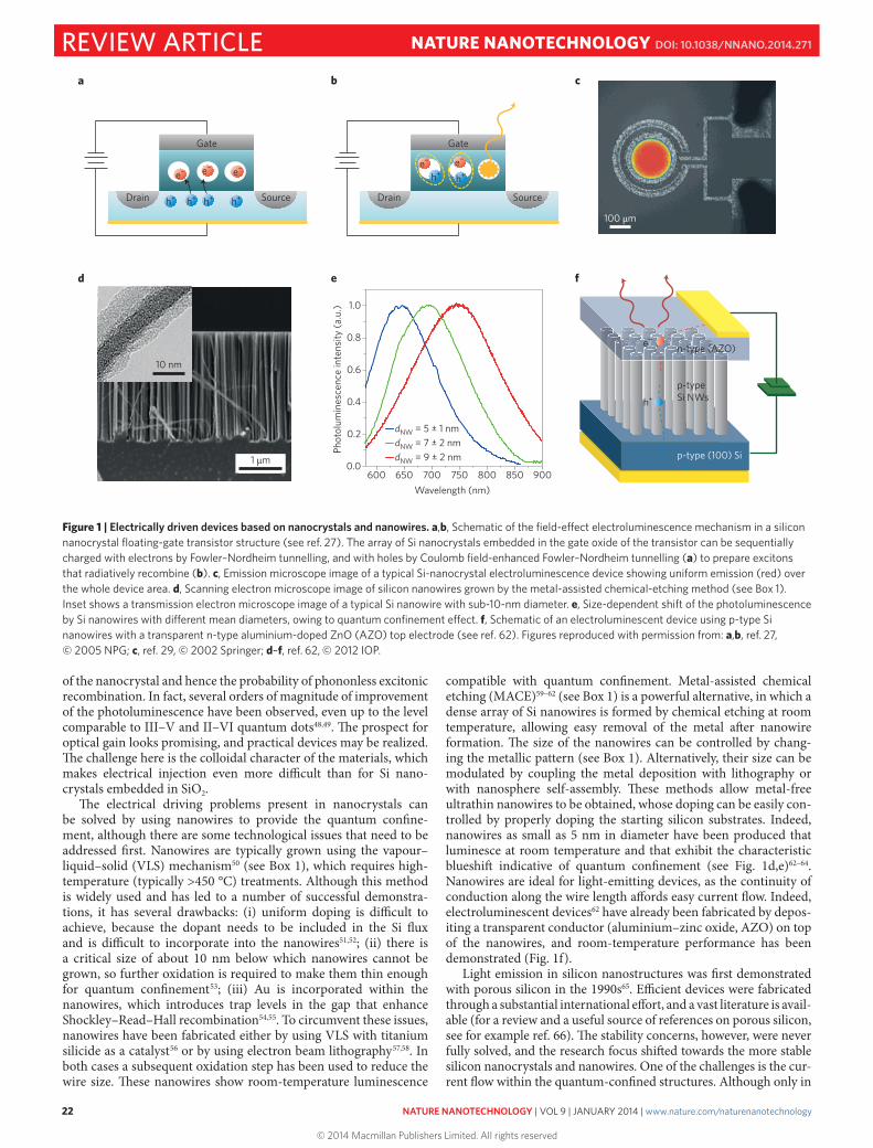
sequential electron and hole injection. Such sequential injection may be realized in a metal–oxide–semiconductor field-effect tran-sistor (MOSFET) structure, with the Si nanocrystals being placed as a floating gate, and electrons and holes being sequentially injected by tunnelling through a thin oxide layer (Fig. 1a,b), using an a.c. voltage of typically 10 kHz (ref. 27). Indeed, luminescence is lower at lower frequency because there are only a few recombination events per unit time, but luminescence decreases again at higher fre-quencies because sequential injection occurs more rapidly than the radiative lifetime in silicon nanocrystals. Defect-mediated emission
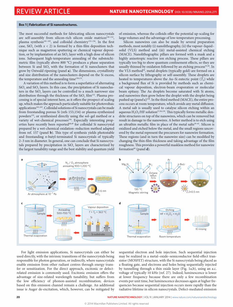
The most successful methods for fabricating silicon nanocrystals are self-assembly from silicon-rich silicon oxide matrices150–152, plasma synthesis101–105, and colloidal chemistry153–156. In the first case, SiOx (with x < 2) is formed by a thin-film deposition tech-nique such as magnetron sputtering or chemical vapour deposi-tion, or by implantation of an SiO2 layer with a high dose of silicon ions. Subsequent high-temperature annealing of the substoichi-metric film (typically above 800 °C) produces a phase separation between Si and SiO2 with the formation of Si nanoclusters that grow by Ostwald ripening (panel a). The dimensions, crystallinity and size distribution of the nanoclusters depend on the Si excess, the temperature and the annealing time150,151.
A variation of this method is to form a superlattice of alternating SiOx and SiO2 layers. In this case, the precipitation of Si nanoclus-ters in the SiOx layers can be controlled to a much narrower size distribution through the thickness of the SiOx film152. Plasma pro-cessing is of special interest here, as it offers the prospect of scaling up, which makes the approach particularly suitable for photovoltaic applications101,105. Colloidal solutions of Si nanocrystals can be made from freestanding porous Si (refs 153,154) or plasma-synthesized powders155, or synthesized directly using the sol–gel method or a variety of wet-chemical processes156. Especially interesting prop-erties have recently been reported48,49 for colloidal Si nanocrystal prepared by a wet-chemical oxidation–reduction method adapted from ref. 157 (panel b). This type of synthesis yields photostable and freestanding n-butyl-terminated Si nanocrystals of typically 2–3 nm in diameter. In general, one can conclude that Si nanocrys-tals prepared by precipitation in SiOx layers are characterized by the largest tunability range and the best stability and quantum yield
of emission, whereas the colloids offer the potential up-scaling for large volumes and the advantage of low-temperature processing.
Silicon nanowires can also be made by several preparation methods, most notably (i) nanolithography, (ii) the vapour–liquid–solid (VLS) method and (iii) metal-assisted chemical etching (MACE). Nanolithographic pillars are formed with a mask and a highly anisotropic reactive ion etching process. These pillars are typically too big to show quantum confinement effects, so they are usually thinned by oxidation followed by an etching process55,56. In the VLS method50, metal droplets (typically gold) are formed on a silicon surface by lithography or self-assembly. These droplets are heated to temperatures above the Au–Si eutectic point (TE) while a background flux of Si is provided by methods such as chemi-cal vapour deposition, electron-beam evaporation or molecular beam epitaxy. The Au droplets become saturated with Si atoms, and nanowires then grow below the droplet with the droplet being pushed up (panel c)158. In the third method (MACE), the entire pro-cess occurs at room temperature, which avoids any metal diffusion. A metal salt is usually used to catalyse silicon etching within an aqueous H2O2/HF solution57,58,159. This typically forms metallic den-drite structures on top of the nanowires, which can be removed but result in damage to the nanowires. A better method is to etch using an ultrathin metallic film in place of the metal salts59–61. Silicon is oxidized and etched below the metal, and the small regions uncov-ered by the metal represent the precursors for nanowire formation. These regions (and in turn the nanowire size) can be modified by changing the thin-film thickness and taking advantage of the film roughness. This provides a powerful maskless method for nanowire formation60 (panel d).
Box 1 | Fabrication of Si nanostructures.
SiSiSi
SiSi
Sample
Sample
Au
Thermal evaporation
Sample
Au
dc
ba
Thermal evaporation
Annealing500–700 °C HF + H2O2 + H2O
Room temperature
Etching
Kl rinsing
Vapour deposition
Si substrate
Si
T > TE = 363 °C
Si SiSiO2
SiOx
N2 / O2 atmosphereannealing 900–1,200 °C
Mg2Si Br2
Ar
Ar atmosphere at 10−7 Pa
130 °CMagnetic stirring 2.2±0.5 nm
Octanereflux72 h
n-BuLi
Ar
3–6 nm
SiSi Si
Br BrBrBr
BrBrBr
BrBrBr
REVIEW ARTICLE NATURE NANOTECHNOLOGY DOI: 10.1038/NNANO.2014.271
© 2014 Macmillan Publishers Limited. All rights reserved
NATURE NANOTECHNOLOGY | VOL 9 | JANUARY 2014 | www.nature.com/naturenanotechnology 21
(oxygen or carbon-related) has proved to be more successful, and devices with higher efficiencies have been reported28. All of these devices are typically MOS-like structures with the oxide replaced by a nanocrystal-rich insulator (oxide or nitride)29,30 (Fig. 1c). Alternatively, light-emitting devices with efficiencies of a few per cent have been fabricated with nanocrystal–organic hybrids31. We note, however, that so far no light-emitting devices based on Si nanocrystals have reached the market. Equally, a Si nanocrystal-based laser, despite initial successful observations of gain32–37, has not yet been developed. One plausible yet less explored route for light emission is hot-carrier recombination, where the advantage of nanocrystals is the mitigation of phonon scattering under quan-tum confinement conditions. Such reduced phonon scattering slows down hot-carrier cooling, thereby enabling light emission by the phononless recombination of hot carriers, whose quantum yield increases by up to three orders of magnitude when compared with bulk Si (from 10–7 to 10–4)38.
Although many interesting approaches for emission from direct transitions have been explored, success has been limited. The indirect approach looks more promising, especially with nanocrystals serving as sensitizers for rare-earth-doped insulating (SiO2) or semi-insulat-ing (Si-rich silicon oxides or nitrides) matrices. Here, the most popu-lar system is that of Er3+ ions in SiO2. Following the initial observation that Er3+ ions can be indirectly excited through photon absorption by Si nanocrystals39–41, practical devices with efficiencies above the per cent level have now been demonstrated30,42–45. Despite this encourag-ing performance, only a minor fraction of all Er dopants are excited, owing to the statistical distribution of Er3+ ions and nanocrystals46,47, thus precluding population inversion and laser action.
A possible breakthrough to resolve this low excitation fraction could come from surface and/or strain engineering. For example, a considerable modification of the wavefunction for the low-energy electron states can be achieved by terminating colloidal nano-crystals with carbon. This termination changes the energy structure
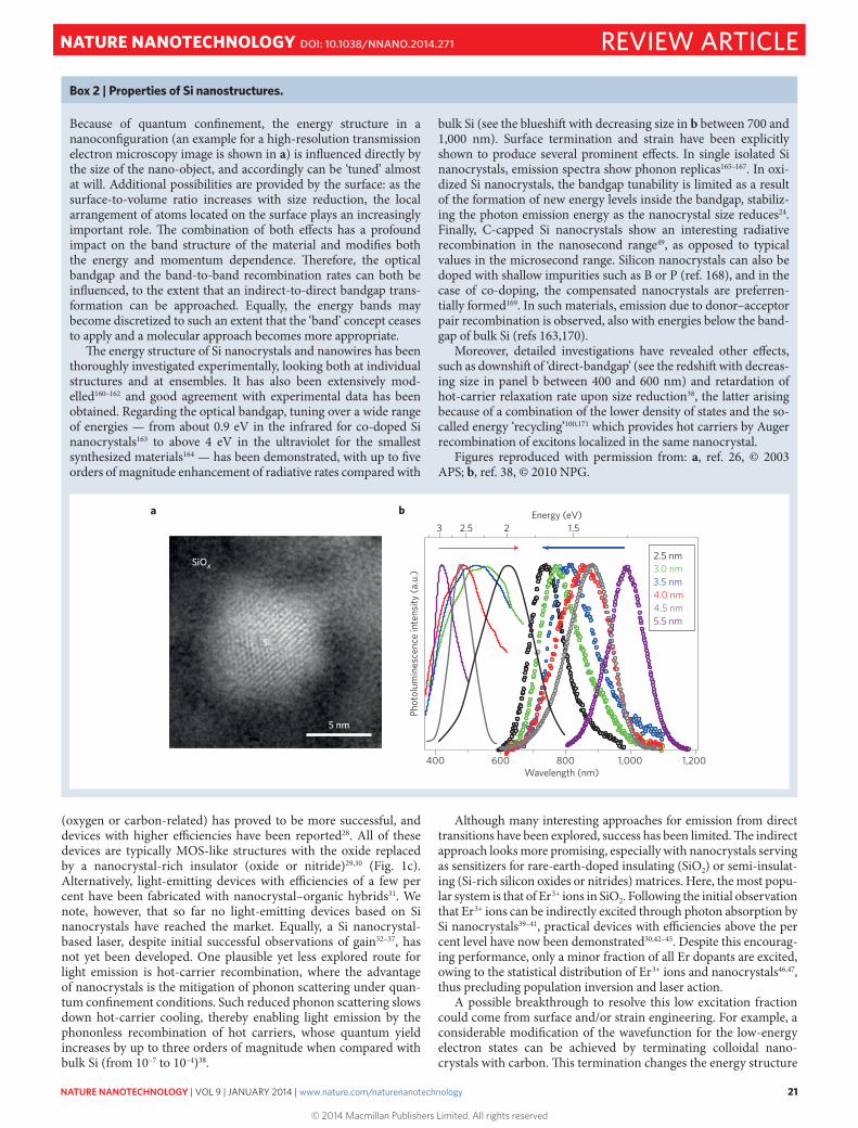
Because of quantum confinement, the energy structure in a nanoconfiguration (an example for a high-resolution transmission electron microscopy image is shown in a) is influenced directly by the size of the nano-object, and accordingly can be ‘tuned’ almost at will. Additional possibilities are provided by the surface: as the surface-to-volume ratio increases with size reduction, the local arrangement of atoms located on the surface plays an increasingly important role. The combination of both effects has a profound impact on the band structure of the material and modifies both the energy and momentum dependence. Therefore, the optical bandgap and the band-to-band recombination rates can both be influenced, to the extent that an indirect-to-direct bandgap trans-formation can be approached. Equally, the energy bands may become discretized to such an extent that the ‘band’ concept ceases to apply and a molecular approach becomes more appropriate.
The energy structure of Si nanocrystals and nanowires has been thoroughly investigated experimentally, looking both at individual structures and at ensembles. It has also been extensively mod-elled160–162 and good agreement with experimental data has been obtained. Regarding the optical bandgap, tuning over a wide range of energies — from about 0.9 eV in the infrared for co-doped Si nanocrystals163 to above 4 eV in the ultraviolet for the smallest synthesized materials164 — has been demonstrated, with up to five orders of magnitude enhancement of radiative rates compared with
bulk Si (see the blueshift with decreasing size in b between 700 and 1,000 nm). Surface termination and strain have been explicitly shown to produce several prominent effects. In single isolated Si nanocrystals, emission spectra show phonon replicas165–167. In oxi-dized Si nanocrystals, the bandgap tunability is limited as a result of the formation of new energy levels inside the bandgap, stabiliz-ing the photon emission energy as the nanocrystal size reduces24. Finally, C-capped Si nanocrystals show an interesting radiative recombination in the nanosecond range49, as opposed to typical values in the microsecond range. Silicon nanocrystals can also be doped with shallow impurities such as B or P (ref. 168), and in the case of co-doping, the compensated nanocrystals are preferren-tially formed169. In such materials, emission due to donor–acceptor pair recombination is observed, also with energies below the band-gap of bulk Si (refs 163,170).
Moreover, detailed investigations have revealed other effects, such as downshift of ‘direct-bandgap’ (see the redshift with decreas-ing size in panel b between 400 and 600 nm) and retardation of hot-carrier relaxation rate upon size reduction38, the latter arising because of a combination of the lower density of states and the so-called energy ‘recycling’100,171 which provides hot carriers by Auger recombination of excitons localized in the same nanocrystal.
Figures reproduced with permission from: a, ref. 26, © 2003 APS; b, ref. 38, © 2010 NPG.
Box 2 | Properties of Si nanostructures.
400 600 800 1,000 1,200
3 2.5 2 1.5
2.5 nm3.0 nm 3.5 nm4.0 nm
5.5 nm4.5 nm
Wavelength (nm)
Energy (eV)
Phot
olum
ines
cenc
e in
tens
ity (a
.u.)
a b
5 nm
SiOx
Si
REVIEW ARTICLENATURE NANOTECHNOLOGY DOI: 10.1038/NNANO.2014.271
© 2014 Macmillan Publishers Limited. All rights reserved
22 NATURE NANOTECHNOLOGY | VOL 9 | JANUARY 2014 | www.nature.com/naturenanotechnology
of the nanocrystal and hence the probability of phononless excitonic recombination. In fact, several orders of magnitude of improvement of the photoluminescence have been observed, even up to the level comparable to III–V and II–VI quantum dots48,49. The prospect for optical gain looks promising, and practical devices may be realized. The challenge here is the colloidal character of the materials, which makes electrical injection even more difficult than for Si nano-crystals embedded in SiO2.
The electrical driving problems present in nanocrystals can be solved by using nanowires to provide the quantum confine-ment, although there are some technological issues that need to be addressed first. Nanowires are typically grown using the vapour–liquid–solid (VLS) mechanism50 (see Box 1), which requires high-temperature (typically >450 °C) treatments. Although this method is widely used and has led to a number of successful demonstra-tions, it has several drawbacks: (i) uniform doping is difficult to achieve, because the dopant needs to be included in the Si flux and is difficult to incorporate into the nanowires51,52; (ii) there is a critical size of about 10 nm below which nanowires cannot be grown, so further oxidation is required to make them thin enough for quantum confinement53; (iii) Au is incorporated within the nanowires, which introduces trap levels in the gap that enhance Shockley–Read–Hall recombination54,55. To circumvent these issues, nanowires have been fabricated either by using VLS with titanium silicide as a catalyst56 or by using electron beam lithography57,58. In both cases a subsequent oxidation step has been used to reduce the wire size. These nanowires show room-temperature luminescence
compatible with quantum confinement. Metal-assisted chemical etching (MACE)59–62 (see Box 1) is a powerful alternative, in which a dense array of Si nanowires is formed by chemical etching at room temperature, allowing easy removal of the metal after nanowire formation. The size of the nanowires can be controlled by chang-ing the metallic pattern (see Box 1). Alternatively, their size can be modulated by coupling the metal deposition with lithography or with nanosphere self-assembly. These methods allow metal-free ultrathin nanowires to be obtained, whose doping can be easily con-trolled by properly doping the starting silicon substrates. Indeed, nanowires as small as 5 nm in diameter have been produced that luminesce at room temperature and that exhibit the characteristic blueshift indicative of quantum confinement (see Fig. 1d,e)62–64. Nanowires are ideal for light-emitting devices, as the continuity of conduction along the wire length affords easy current flow. Indeed, electroluminescent devices62 have already been fabricated by depos-iting a transparent conductor (aluminium–zinc oxide, AZO) on top of the nanowires, and room-temperature performance has been demonstrated (Fig. 1f).
Light emission in silicon nanostructures was first demonstrated with porous silicon in the 1990s65. Efficient devices were fabricated through a substantial international effort, and a vast literature is avail-able (for a review and a useful source of references on porous silicon, see for example ref. 66). The stability concerns, however, were never fully solved, and the research focus shifted towards the more stable silicon nanocrystals and nanowires. One of the challenges is the cur-rent flow within the quantum-confined structures. Although only in
100 µm
dNW = 5 ± 1 nmdNW = 7 ± 2 nmdNW = 9 ± 2 nm
c
d e f
Gate
a b
e− e−
h+Drain Sourceh+ h+ h+
e−
Gate
Drain Source
10 nm
1 µm600 650 700 750 800 850 900
Wavelength (nm)
1.0
0.8
0.6
0.4
0.2
0.0
Phot
olum
ines
cenc
e in
tens
ity (a
.u.)
h+ h+e− e−
h+
p-typeSi NWs
n-type (AZO)
p-type (100) Si
e−
Figure 1 | Electrically driven devices based on nanocrystals and nanowires. a,b, Schematic of the field-effect electroluminescence mechanism in a silicon nanocrystal floating-gate transistor structure (see ref. 27). The array of Si nanocrystals embedded in the gate oxide of the transistor can be sequentially charged with electrons by Fowler–Nordheim tunnelling, and with holes by Coulomb field-enhanced Fowler–Nordheim tunnelling (a) to prepare excitons that radiatively recombine (b). c, Emission microscope image of a typical Si-nanocrystal electroluminescence device showing uniform emission (red) over the whole device area. d, Scanning electron microscope image of silicon nanowires grown by the metal-assisted chemical-etching method (see Box 1). Inset shows a transmission electron microscope image of a typical Si nanowire with sub-10-nm diameter. e, Size-dependent shift of the photoluminescence by Si nanowires with different mean diameters, owing to quantum confinement effect. f, Schematic of an electroluminescent device using p-type Si nanowires with a transparent n-type aluminium-doped ZnO (AZO) top electrode (see ref. 62). Figures reproduced with permission from: a,b, ref. 27, © 2005 NPG; c, ref. 29, © 2002 Springer; d–f, ref. 62, © 2012 IOP.
REVIEW ARTICLE NATURE NANOTECHNOLOGY DOI: 10.1038/NNANO.2014.271
© 2014 Macmillan Publishers Limited. All rights reserved
NATURE NANOTECHNOLOGY | VOL 9 | JANUARY 2014 | www.nature.com/naturenanotechnology 23
its infancy, we believe that the silicon nanowire approach offers a very promising route towards efficient silicon-based light sources.
Nanopatterning. The ability to control the flow of light with pho-tonic crystals (PhCs)67 has added tremendous functionality to the silicon photonic toolkit. The full benefit of PhC light confinement is derived from three-dimensional (3D) structures, but these tend to be very difficult to make and control. Instead, researchers have made impressive progress with 2D structures that rely on total internal reflection for confinement in the third dimension68,69 (see Box 3). In fact, a key reason for the success of silicon nanotechnol-ogy in this field is that high-quality silicon-on-insulator (SOI) sub-strates are readily available and that fabrication is relatively simple and reliable; the best results are being achieved from electron-beam lithography with the resist (typically ZEP-520A) being directly used as a masking layer70. Another important feature is that some of the best results have been achieved on tools that are readily available in many laboratories; a good converted scanning electron microscope (SEM) as an electron-beam lithography tool and a basic parallel-plate reactive ion etching system may be sufficient, which is why PhC research has proliferated and many groups are engaged.
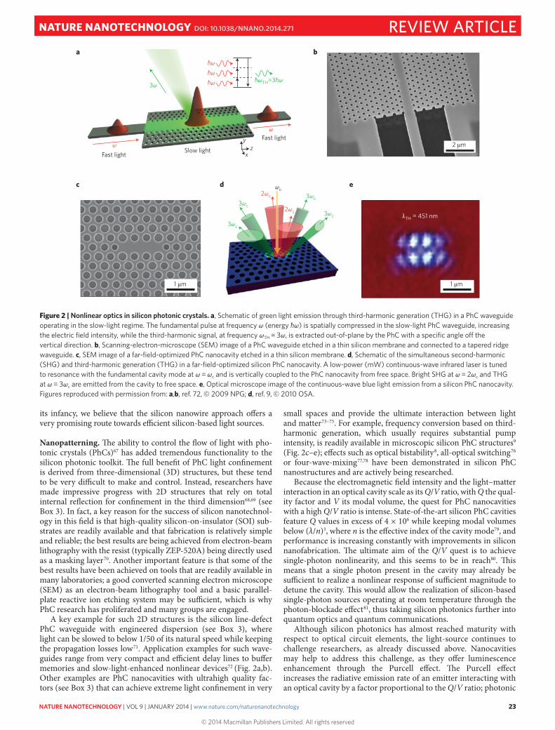
A key example for such 2D structures is the silicon line-defect PhC waveguide with engineered dispersion (see Box 3), where light can be slowed to below 1/50 of its natural speed while keeping the propagation losses low71. Application examples for such wave-guides range from very compact and efficient delay lines to buffer memories and slow-light-enhanced nonlinear devices72 (Fig. 2a,b). Other examples are PhC nanocavities with ultrahigh quality fac-tors (see Box 3) that can achieve extreme light confinement in very
small spaces and provide the ultimate interaction between light and matter73–75. For example, frequency conversion based on third-harmonic generation, which usually requires substantial pump intensity, is readily available in microscopic silicon PhC structures9
(Fig. 2c–e); effects such as optical bistability8, all-optical switching76 or four-wave-mixing77,78 have been demonstrated in silicon PhC nanostructures and are actively being researched.
Because the electromagnetic field intensity and the light–matter interaction in an optical cavity scale as its Q/V ratio, with Q the qual-ity factor and V its modal volume, the quest for PhC nanocavities with a high Q/V ratio is intense. State-of-the-art silicon PhC cavities feature Q values in excess of 4 × 10⁶ while keeping modal volumes below (λ/n)3, where n is the effective index of the cavity mode79, and performance is increasing constantly with improvements in silicon nanofabrication. The ultimate aim of the Q/V quest is to achieve single-photon nonlinearity, and this seems to be in reach80. This means that a single photon present in the cavity may already be sufficient to realize a nonlinear response of sufficient magnitude to detune the cavity. This would allow the realization of silicon-based single-photon sources operating at room temperature through the photon-blockade effect81, thus taking silicon photonics further into quantum optics and quantum communications.
Although silicon photonics has almost reached maturity with respect to optical circuit elements, the light-source continues to challenge researchers, as already discussed above. Nanocavities may help to address this challenge, as they offer luminescence enhancement through the Purcell effect. The Purcell effect increases the radiative emission rate of an emitter interacting with an optical cavity by a factor proportional to the Q/V ratio; photonic
c d e
aħω
ħωTH=3ħωħωħω3ω
ω
ωFast light
x
yz
Fast lightSlow light
2 µm
b
1 µm
λTH = 451 nm
1 µm
3ωc
3ωc
3ωc
3ωc
2ωc
2ωc
ωc
Figure 2 | Nonlinear optics in silicon photonic crystals. a, Schematic of green light emission through third-harmonic generation (THG) in a PhC waveguide operating in the slow-light regime. The fundamental pulse at frequency ω (energy ħω) is spatially compressed in the slow-light PhC waveguide, increasing the electric field intensity, while the third-harmonic signal, at frequency ωTH = 3ω, is extracted out-of-plane by the PhC with a specific angle off the vertical direction. b, Scanning-electron-microscope (SEM) image of a PhC waveguide etched in a thin silicon membrane and connected to a tapered ridge waveguide. c, SEM image of a far-field-optimized PhC nanocavity etched in a thin silicon membrane. d, Schematic of the simultaneous second-harmonic (SHG) and third-harmonic generation (THG) in a far-field-optimized silicon PhC nanocavity. A low-power (mW) continuous-wave infrared laser is tuned to resonance with the fundamental cavity mode at ω = ωc and is vertically coupled to the PhC nanocavity from free space. Bright SHG at ω = 2ωc and THG at ω = 3ωc are emitted from the cavity to free space. e, Optical microscope image of the continuous-wave blue light emission from a silicon PhC nanocavity. Figures reproduced with permission from: a,b, ref. 72, © 2009 NPG; d, ref. 9, © 2010 OSA.
REVIEW ARTICLENATURE NANOTECHNOLOGY DOI: 10.1038/NNANO.2014.271
© 2014 Macmillan Publishers Limited. All rights reserved
24 NATURE NANOTECHNOLOGY | VOL 9 | JANUARY 2014 | www.nature.com/naturenanotechnology
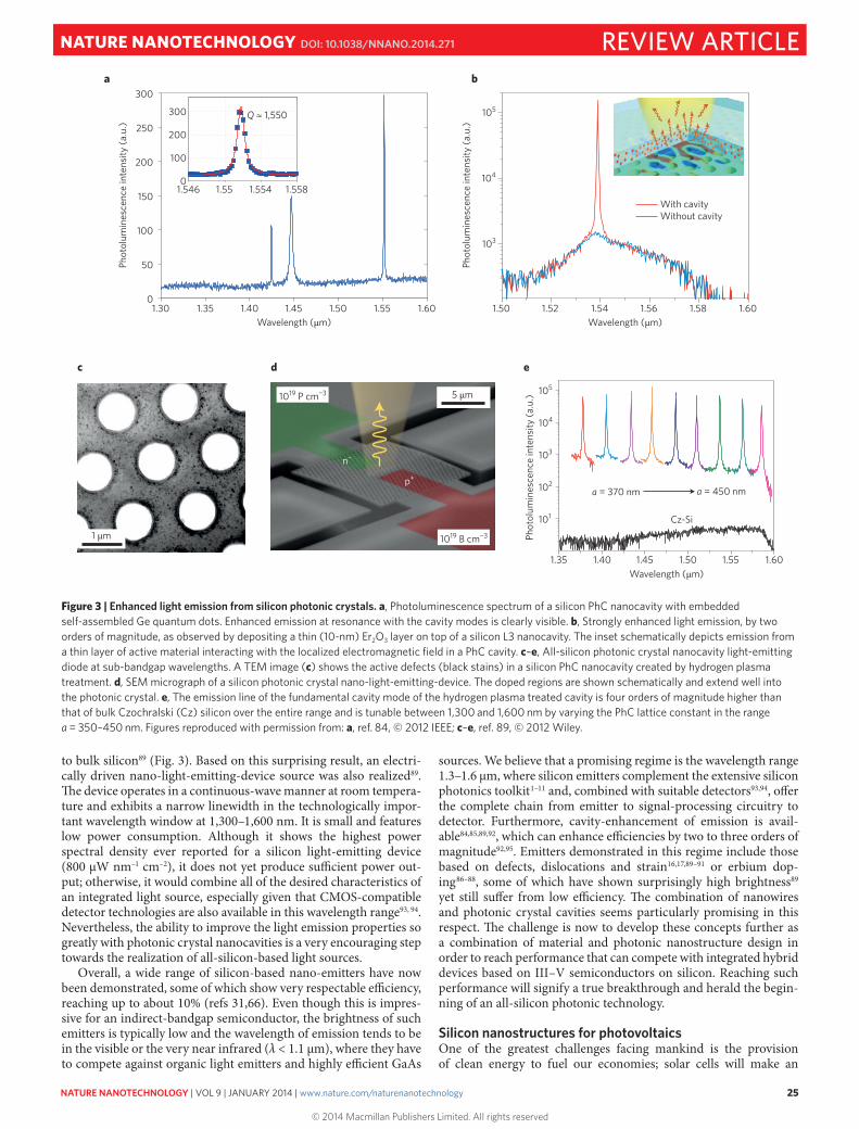
crystal cavities feature the highest Q/V ratio of any known cavity type. Indeed, enhanced emission from band-edge luminescence has already been observed with silicon PhC nanocavities resonant in the 1.1-μm range82,83, and strong emission lines at 1.3–1.6 μm have been observed in Ge self-assembled quantum dots embed-ded in silicon PhC nanocavities84,85. Moreover, the incorporation of erbium ions in silicon nitride PhC nanocavities has enabled optically pumped transparency at 1.54 μm (refs 86,87), and recent research has shown that a thin film of erbium dioxide deposited onto a silicon nano cavity may be driven close to inversion, even at room temperature88.
Optically active defects may also be introduced directly into silicon high-Q PhC nanocavities using a simple hydrogen plasma treatment89. The sub-bandgap luminescence from defects such as dislocation loops or hydrogen platelets is well studied17,90,91, but notoriously quenches very quickly with temperature, making light-emitting devices based on these active centres impractical. Recently, the application of the Purcell effect combined with the improved extraction efficiency from a far-field-engineered PhC nanocavity (Box 3) has proved very effective in suppressing thermal quenching up to room temperature92 and has led to an overall enhancement of light emission by more than four orders of magnitudes relative
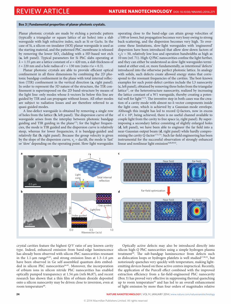
Planar photonic crystals are made by etching a periodic pattern (typically a triangular or square lattice of air holes) into a slab waveguide with high refractive index, such as Si or GaAs. In the case of Si, a silicon-on-insulator (SOI) planar waveguide is used as the starting material, and the patterned PhC membrane is released by removing the lower SiO2 cladding with a HF-based wet etch (a, left panel). Typical parameters for Si PhC slabs operating at λ = 1.55 μm are a lattice constant of a = 420 nm, a slab thickness of t = 220 nm and a hole radius of r = 130 nm (ratio r/a ≈ 0.3).
Planar photonic crystals are able to provide efficient optical confinement in all three dimensions by combining the 2D pho-tonic bandgap confinement in the plane with total internal reflec-tion (TIR) confinement in the vertical direction (a, right panel). In order to represent the 3D nature of the structure, the TIR con-finement is superimposed on the 2D band-structure by means of the light line: only modes whose k-vectors lie below this line are guided by TIR and can propagate without losses. All other modes are subject to radiation losses and are therefore referred to as quasi-guided modes.
A line-defect waveguide is obtained by removing a single row of holes from the lattice (b, left panel). The dispersion curve of the waveguide arises from the interplay between photonic bandgap guiding and TIR guiding in the plane172; for the higher frequen-cies, the mode is TIR guided and the dispersion curve is relatively steep, whereas for lower frequencies, it is bandgap-guided and relatively flat (b, right panel). Because the group velocity is given by the slope of the dispersion curve, vg = dω/dk, the mode is ‘fast’ or ‘slow’ depending on the operating point. Slow-light waveguides
operating close to the band-edge can attain group velocities of c/100 or lower, but propagation becomes very lossy owing to strong back-scattering, and the dispersion becomes very high. To over-come these limitations, slow-light waveguides with ‘engineered’ dispersion have been introduced that allow slow-down factors of vg/c = 50, relatively low loss and operation bandwidths as high as 10 nm (ref. 71). High-Q PhC nanocavities confine the light further, and they can either be understood as slow-light waveguides termi-nated at either end, or, more fundamentally, as intentional ‘defects’ introduced into the otherwise perfect photonic lattice. In analogy with solids, such defects create allowed energy states that corre-spond to the resonant frequencies of the cavities. The best-known examples for such point-defect cavities include the L3 nanocavity (c, left panel), obtained by removing three holes from the triangular lattice72, or the heterostructure nanocavity, realized by increasing the lattice constant of a W1 waveguide, thereby creating a poten-tial well for light72,74. The inventive step in both cases was the crea-tion of a cavity mode with almost no k-vector components inside the light cone, which is achieved by a Gaussian-mode envelope. Although this insight has led to record Q-factors, now in excess of 4 × 10⁶, being achieved, there is no useful channel available to couple light from the cavity to free space (c, right panel). By super-imposing a secondary lattice consisting of slightly enlarged holes (d, left panel), we have been able to engineer the far field into a near-Gaussian output beam (d, right panel) while hardly compro-mising the cavity Q-factor173,174. Such far-field engineering has been instrumental for the successful observation of strongly enhanced linear and nonlinear light emission9,88,89,92.
Box 3 | Fundamental properties of planar photonic crystals.
0.0 0.5 1.0
Ener
gy
Wavevector (π/a)
y x
z
Lightcone Total internal
reflection
Index guided
Gap guidedLight line
Far-field optimization
a
b
c
d
30°90°
60°
Near field Far field
90°30°
60°
0.5 µm
1 µm
Near field Far field
REVIEW ARTICLE NATURE NANOTECHNOLOGY DOI: 10.1038/NNANO.2014.271
© 2014 Macmillan Publishers Limited. All rights reserved
NATURE NANOTECHNOLOGY | VOL 9 | JANUARY 2014 | www.nature.com/naturenanotechnology 25
to bulk silicon89 (Fig. 3). Based on this surprising result, an electri-cally driven nano-light-emitting-device source was also realized89. The device operates in a continuous-wave manner at room tempera-ture and exhibits a narrow linewidth in the technologically impor-tant wavelength window at 1,300–1,600 nm. It is small and features low power consumption. Although it shows the highest power spectral density ever reported for a silicon light-emitting device (800 μW nm–1 cm–2), it does not yet produce sufficient power out-put; otherwise, it would combine all of the desired characteristics of an integrated light source, especially given that CMOS-compatible detector technologies are also available in this wavelength range93, 94. Nevertheless, the ability to improve the light emission properties so greatly with photonic crystal nanocavities is a very encouraging step towards the realization of all-silicon-based light sources.
Overall, a wide range of silicon-based nano-emitters have now been demonstrated, some of which show very respectable efficiency, reaching up to about 10% (refs 31,66). Even though this is impres-sive for an indirect-bandgap semiconductor, the brightness of such emitters is typically low and the wavelength of emission tends to be in the visible or the very near infrared (λ < 1.1 μm), where they have to compete against organic light emitters and highly efficient GaAs
sources. We believe that a promising regime is the wavelength range 1.3–1.6 μm, where silicon emitters complement the extensive silicon photonics toolkit1–11 and, combined with suitable detectors93,94, offer the complete chain from emitter to signal-processing circuitry to detector. Furthermore, cavity-enhancement of emission is avail-able84,85,89,92, which can enhance efficiencies by two to three orders of magnitude92,95. Emitters demonstrated in this regime include those based on defects, dislocations and strain16,17,89–91 or erbium dop-ing86–88, some of which have shown surprisingly high brightness89 yet still suffer from low efficiency. The combination of nanowires and photonic crystal cavities seems particularly promising in this respect. The challenge is now to develop these concepts further as a combination of material and photonic nanostructure design in order to reach performance that can compete with integrated hybrid devices based on III–V semiconductors on silicon. Reaching such performance will signify a true breakthrough and herald the begin-ning of an all-silicon photonic technology.
Silicon nanostructures for photovoltaicsOne of the greatest challenges facing mankind is the provision of clean energy to fuel our economies; solar cells will make an
Figure 3 | Enhanced light emission from silicon photonic crystals. a, Photoluminescence spectrum of a silicon PhC nanocavity with embedded self-assembled Ge quantum dots. Enhanced emission at resonance with the cavity modes is clearly visible. b, Strongly enhanced light emission, by two orders of magnitude, as observed by depositing a thin (10-nm) Er2O3 layer on top of a silicon L3 nanocavity. The inset schematically depicts emission from a thin layer of active material interacting with the localized electromagnetic field in a PhC cavity. c–e, All-silicon photonic crystal nanocavity light-emitting diode at sub-bandgap wavelengths. A TEM image (c) shows the active defects (black stains) in a silicon PhC nanocavity created by hydrogen plasma treatment. d, SEM micrograph of a silicon photonic crystal nano-light-emitting-device. The doped regions are shown schematically and extend well into the photonic crystal. e, The emission line of the fundamental cavity mode of the hydrogen plasma treated cavity is four orders of magnitude higher than that of bulk Czochralski (Cz) silicon over the entire range and is tunable between 1,300 and 1,600 nm by varying the PhC lattice constant in the range a = 350–450 nm. Figures reproduced with permission from: a, ref. 84, © 2012 IEEE; c–e, ref. 89, © 2012 Wiley.
1019 B cm−3
1.50 1.52 1.54 1.56 1.58 1.60
103
104
105
With cavityWithout cavity
Phot
olum
ines
cenc
e in
tens
ity (a
.u.)
1.35 1.40 1.45 1.50 1.55 1.60
101
102
103
104
105
Cz-Si
a = 450 nm
Phot
olum
ines
cenc
e in
tens
ity (a
.u.)
Wavelength (µm)
Wavelength (µm)
a = 370 nm
a
1.30 1.35 1.40 1.45 1.50 1.55 1.60Wavelength (µm)
0
50
100
150
200
250
300
Phot
olum
ines
cenc
e in
tens
ity (a
.u.)
1.546 1.55 1.554 1.5580
100
200
300 Q ≈ 1,550
c d e
b
1 µm
5 µm 1019 P cm−3
n−
p+
REVIEW ARTICLENATURE NANOTECHNOLOGY DOI: 10.1038/NNANO.2014.271
© 2014 Macmillan Publishers Limited. All rights reserved
26 NATURE NANOTECHNOLOGY | VOL 9 | JANUARY 2014 | www.nature.com/naturenanotechnology
important contribution to this challenge as part of the renewable energy mix. Of the many possible materials proposed and dem-onstrated for making photovoltaic solar cells, silicon is the only one that combines suitable optoelectronic properties with Earth-abundance and technological availability. Currently the highest demonstrated photovoltaic conversion efficiency of a Si solar cell is near 25%, which has been realized in a single junction configu-ration96. This is very close to the Shockley–Queisser limit of about 30% (ref. 97), and therefore only limited further progress can be expected. At the same time, Si tandems that make use of crystalline, micro/polycrystalline and amorphous forms of Si have not been able to surpass this efficiency. Consequently, the value of 25% represents the general present-day record efficiency for Si-based photovoltaics. Wafer-based ‘bulk’ silicon cells currently dominate the market, yet only thin-film cells will be cost-effective in the long run, as they do not require much active material and can be produced cheaply using flow-through processes on metre-sized substrates. The main trade-off of thin-film versus bulk solar cells is their reduced absorp-tion, which introduces the need for light-trapping schemes that increase the effective absorption length of the thin-film material. Nanopatterning, quantum confinement and surface-induced effects in Si nanostructures offer interesting features that could be used to boost the efficiency of photovoltaic energy conversion and to overcome some of the restraints that lead to the Shockley–Queisser limit98. Specific ‘photovoltaic opportunities’ follow from (i) the pos-sibility of bandgap engineering, through nanocrystals and nanow-ires, to modify absorption and extraction, and (ii) the possibility of new light-trapping schemes through nanopatterning.
Nanocrystals and nanowires. Silicon nanocrystals present several properties of importance for photovoltaics: (i) the possibility of tun-ing the bandgap and the recombination rate through quantum con-finement and dedicated surface termination, (ii) the reduction of the density of states and discretization of energy levels that affect hot-carrier cooling processes, and (iii) the enhancement of the Coulomb interaction between carriers enclosed in small volumes, promoting collective effects such as multiple carrier generation (MEG)99 and ‘Auger recycling’100. But these advantageous properties do not arise without a price: the potential barrier that aids quantum confine-ment also impedes carrier extraction to the outside. In particular, this problem is notorious in all concepts of (the third-generation) solar cells based on nanocrystals. For the most readily available and most investigated system of Si nanocrystals in the solid matrix of SiO2, the relevant potential barrier for free electrons is around 3 eV. Therefore, extraction of photogenerated carriers has to invoke tunnelling and percolation between closely spaced nanocrystals (forming ‘quantum solids’) which is not efficient. Several different approaches are under investigation, such as the fabrication of Si nanocrystal/organic hybrid solar cells101. Nanocrystals can be pro-duced by plasma processing with the advantage of a scalable mass production for photovoltaic devices101–105. Demonstrated power conversion efficiencies are limited to a few per cent101, because of the low carrier mobility, although progress can be expected. Indeed, the formation of defect/impurity-related minibands linking indi-vidual nanocrystals106, or dispersions in several conducting media (macroporous TiO2, polymers), is also under investigation. It seems that the ultimate solution would be a highly conductive medium with only a minimal conduction-band offset; some investigations suggest that a potential barrier as small as 0.1 eV would be sufficient to preserve advantages of quantum confinement while minimizing extraction loss. Nevertheless, the efficient extraction of free carriers from a confined environment remains a challenge.
An interesting solution to this problem may again be offered by Si nanowires. In analogy with the light-emission discussion, quantum confinement takes place in two dimensions, whereas carriers can be extracted along the third. Silicon nanowire solar cells have already
been fabricated both on a single wire107,108 and on nanowire arrays109. Two main schemes are used110: axial junctions111,112, in which the p–i–n diode is fabricated along the length of the nano wire by varying the doping density during growth; and radial junctions113, in which the diode is fabricated coaxially by a core–shell method. The advan-tages of using silicon nanowires for solar cells are multifold. First of all, nanowire arrays are extremely strong absorbers109,114, as the light remains trapped inside the nanowire forest by multiple scattering events. Second, radial junctions have the advantage of a very short electrical path-length for carrier extraction, which would suggest the potential for significant performance improvements. In fact, efficiency depends on a compromise between the extracted cur-rent (increasing with decreasing nanowire radius) and open-circuit voltage (decreasing with increasing junction area, and hence with decreasing nanowire radius). Optimal radial junctions have a radius similar to the minority-carrier diffusion length to allow full collec-tion without decreasing the voltage too much. A challenge is then to achieve the required high doping density needed to avoid depletion with decreasing nanowire size. In principle, quantum confinement could also be used to build cells in which the nanowires form the top part of a cell, which is transparent to less energetic photons that are absorbed at the bottom.
Both VLS growth and the MACE method have been used suc-cessfully to obtain nanowire solar cells60,112,115. In a nanowire solar cell the nanowire ‘carpet’ can be conformally covered by a transpar-ent electrode such as AZO embedded within a conductive polymer or alternatively infiltrated by a liquid electrode. The resulting solar cells have all the advantages of a highly absorbing material with a radial, low-path, carrier extraction. One might expect that the bet-ter performance is obtained by maximizing carrier extraction and hence carrier lifetime, which is, indeed, achieved by minimizing trap centres. This is in principle easier with the MACE method, as the preparation is at room temperature and the detrimental effect of metal diffusion does not occur. In fact solar cells with efficien-cies over 10% have already been claimed116, with further progress being expected.
Silicon nanostructures not only allow us to make traditional ‘photon-in/electron-out’ photovoltaic devices; they can also form the basis of an autonomous device — a ‘solar shaper’. Such a pho-ton-in/photon-out scheme does not involve carrier extraction, but it would be used to extract energy from the parts of the solar spectrum that are otherwise not efficiently converted. It therefore rectifies the fundamental reason for the limited efficiency of photo-voltaic conversion: the mismatch between the broadband character of solar radiation and the narrow window of optimal performance of a semiconductor photodiode. A solar ‘shaper’ could form an add-on that supplements the traditional cell and converts the incoming broadband spectrum into a new spectrum that is narrower and bet-ter optimized for absorption by a single-junction solar cell. This would require the ‘cutting’ of high-energy ultraviolet photons into multiple lower-energy quanta that can be converted more effi-ciently, as well as the ‘pasting’ together of low-energy photons in the near infrared that are otherwise not converted at all. Silicon nanocrystals offer interesting possibilities that could be used for both processes.
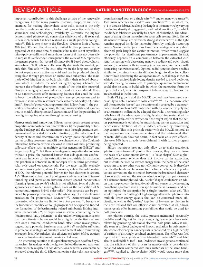
For photon cutting, the MEG process mentioned previously could be used (Fig. 4a). In this process, a highly energetic hot carrier relaxes by generating additional electron–hole pairs. MEG is usu-ally seen as a direct analogue of impact excitation in bulk materi-als, whose efficiency in nanocrystals is enhanced by a high density of carriers in a strongly confined environment. The effect was first reported in nanocrystals of direct-bandgap materials117 and later also in (colloidal) Si (ref. 118). Dedicated investigations confirmed that the efficiency of this process in nanocrystals is considerably enhanced when compared with bulk materials of the same band-gap119,120. Applied to photovoltaics, MEG would create more than
REVIEW ARTICLE NATURE NANOTECHNOLOGY DOI: 10.1038/NNANO.2014.271
© 2014 Macmillan Publishers Limited. All rights reserved
NATURE NANOTECHNOLOGY | VOL 9 | JANUARY 2014 | www.nature.com/naturenanotechnology 27
one electron–hole pair per single absorbed high-energy photon, thereby creating additional photocurrent from the green and blue part of the solar spectrum. Indeed, theoretical evaluations indicate that total conversion efficiencies of up to ~50% are feasible — that is, efficiencies well above the Shockley–Queisser limit121. The life-time of the multiple carriers generated in this process is limited by their Auger interaction and depends on the nanocrystal size and carrier multiplicity, but generally remains in the subnanosecond range121,122, which is too short. For dense solid-state dispersions of Si nanocrystals in SiO2 (ref. 123), however, multiple excitons that are generated on absorption of a single high-energy photon can appear not in the same but in neighbouring nanocrystals100; this spatial separation reduces Auger interaction, allowing for radiative recom-bination of multiple excitons and the emission of several photons of lower energy. Detailed investigations124,125 showed that this process of space-separated quantum cutting (Fig. 4b) can be very efficient, doubling the number of emitted photons for energies as low as 0.3 eV above the energy conservation limit (of 2Egap). Therefore the photon cutting effect could also open new opportunities for even-tual schemes of carrier extraction, because in ‘multiplied’ carriers
the lifetime is increased from the typical subnanosecond range to tens or even hundreds of microseconds.
Recent investigations revealed that Si nanocrystals may also be suitable for photon pasting. The most important properties in this respect are (i) the identification of phononless recombination38, (ii) a significant reduction of the cooling rate for hot carriers, (iii) a large cross-section of free carriers for the absorption of infrared photons, and (iv) defect-related hot-carrier photoluminescence. These prop-erties, especially in combination, open perspectives for photovoltaic conversion of infrared photons that are otherwise lost. Two specific approaches that make use of such combined effects are currently under investigation (see Fig. 4). The first is the absorption of low-energy photons by free carriers for the generation of hot excitons, followed by carrier multiplication, shown in Fig. 4c, or trapping at the Si–O related defect and subsequent ‘blue’ emission at ~420 nm (refs 126,127). We point out that because the 420-nm wavelength of the hot defect-related emission is fixed, the absorption of the infrared photons can be tailored by changing the nanocrystal size, as highlighted in Fig. 4d. A second approach makes use of the non-linear properties of Si nanocrystals, more specifically the combined
Figure 4 | Photon cutting and pasting by Si nanocrystals. a,b, Photon cutting. a, In MEG a hot carrier is created on absorption of a high-energy photon (1), and then cools down by generating a second exciton (2). Efficient Auger interaction allows for photoluminescence (PL) from only one exciton (3). b, In space-separated quantum cutting (SSQC), the excess energy of the hot carrier is used to generate an exciton in a neighbouring (coupled) nanocrystal. The separated excitons are now both able to recombine radiatively. c,d, Photon pasting. c, Absorption of low-energy (below-bandgap) photons by free carriers (generated by photons with Eexc > Egap). The resulting hot carrier can be trapped at a surface-related defect level (420 nm) or undergo spatially separated multiplication. d, Nanocrystals with different bandgap sizes (but with the fixed 420-nm line) can be used to absorb and trap infrared photons of different energy. By tuning the nanocrystal diameter, absorption for specific infrared photons can be optimized.
MEGa b
c d
420 nm
SSQC
420 nm 420 nm
1
2
3
PLAuger
SSQC
1
3PLPL
2
REVIEW ARTICLENATURE NANOTECHNOLOGY DOI: 10.1038/NNANO.2014.271
© 2014 Macmillan Publishers Limited. All rights reserved
28 NATURE NANOTECHNOLOGY | VOL 9 | JANUARY 2014 | www.nature.com/naturenanotechnology
absorption of two (or more) low-energy photons for the generation of a single low-energy electron–hole pair128.
In general, in addition to these opportunities and unique properties, Si nanostructures offer one key advantage over other approaches for next-generation photovoltaics, namely the use of Si itself. Silicon nanostructures add the important degrees of freedom of bandstructure engineering and surface modification to the abun-dance, minimal environmental footprint and technological matu-rity of the Si material.
Light trapping. The main trade-off of thin-film versus bulk solar cells is their reduced absorption, which introduces the need for light-trapping schemes that increase the effective absorption length of the thin-film material. Nanophotonic techniques are particularly promising for the purpose of light trapping, as they allow us to con-trol the flow of light on the length scale of several 100 nm to a few micrometres that is required for thin-film solar cells. Researchers are pursuing two different paradigms, plasmonic and diffractive light trapping; here, we focus on diffractive effects, as we believe that the inevitable absorption incurred by plasmonic nanostructures makes it even more challenging to achieve the desired high efficiencies, and to convert every incoming photon into an electron–hole pair (for a recent review on plasmonics for photovoltaic devices see ref. 129).
The key figure of merit for any light-trapping scheme is the Lambertian limit130,131, which has a maximum value of 4n2 and is a measure for the achievable pathlength compared with a single pass through the material; a photon may travel up to 4n2 times fur-ther than without light trapping, and hence increase its chances of being absorbed. The 4n2 limit assumes very weak absorption, and only applies if the path-length is much smaller than the absorption length; for thicker or more strongly absorbing materials, it is cor-respondingly smaller. For example, for a 100-nm-thick crystalline silicon film, light trapping close to the Lambertian limit may be achieved, whereas a factor of 2 is the most that can be expected for an amorphous Si (a-Si) film of the same thickness132. An additional effect of nanostructures is their ability to completely suppress back-reflections, which has led to the term ‘black silicon’133–135 being used to describe this property.
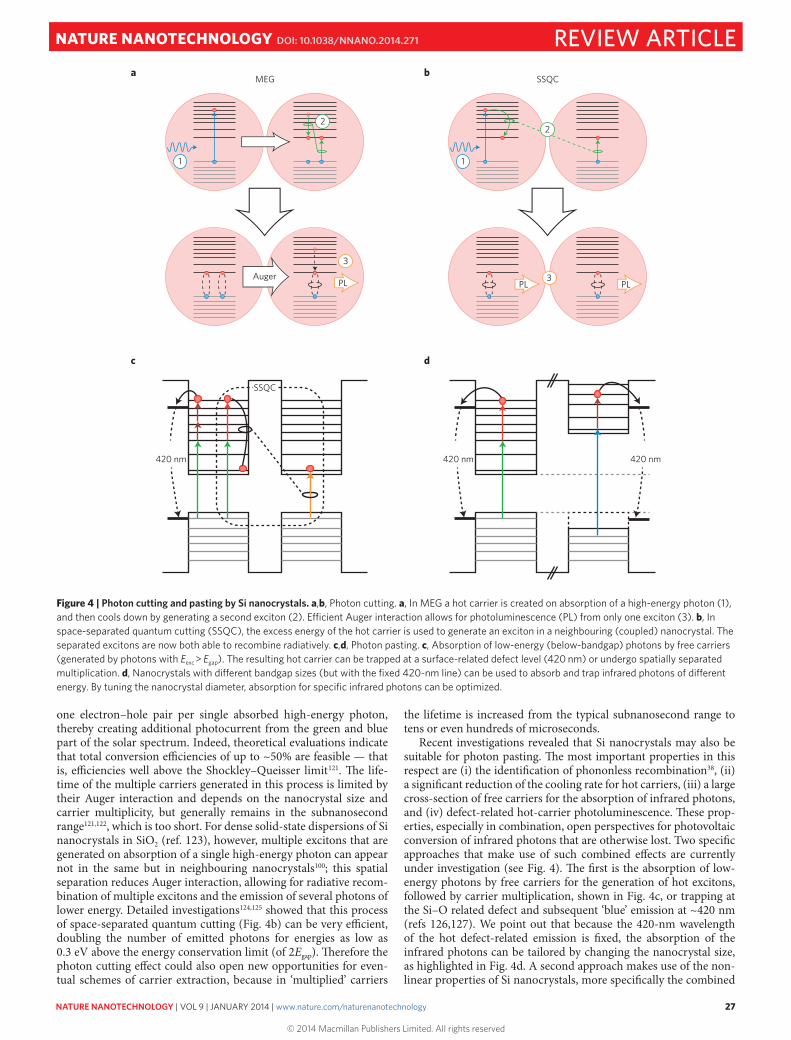
What type of structure to use in order to achieve light trapping in a thin-film solar cell is a question that is actively being researched, with the options ranging from random surface roughness, which excites many diffraction orders, to ordered gratings that only excite a few. Recent trends indicate that the optimum light-trapping structure lies somewhere in-between; the diffraction orders gener-ated by random scattering are too weak, but there are not enough of them created by regular ordered gratings. Furthermore, neither extreme provides sufficient degrees of freedom to account for the wavelength-dependent absorption of the active layer. Accordingly, a number of structures that have been developed using numerical optimization techniques appear quasi-random136 or periodic with a more complex unit cell137,138. Similarly, structures making use of multiple light scattering and wave interference in two-dimensional random media have shown increased light-trapping properties139, as have periodic structures that were partially randomized140 and randomly rough structures with Gaussian disorder141. Structures with more complex three-dimensional unit cells are also being investigated and have shown light-trapping performance close to the Lambertian limit142,143, but they are more challenging to fabri-cate, especially on the large scales required for cost-effective mass-production. The consideration of mass-manufacturability adds an important boundary condition, namely that of simplicity, which drives the search for structures such as binary gratings that are intrinsically easy to make yet still high-performing137,144 (see Fig. 5).
Ultimately, researchers aim to surpass the Lambertian limit, espe-cially as this limit was derived for thick-film cells and relies on geo-metric optics, whereas for thin-film cells, wave optics rules. Proposals for new structures that may surpass this limit in the wave-optics regime and for a limited wavelength range have already been made145, but an experimental structure that surpasses the Lambertian limit for all angles and in the full wavelength region of interest remains elusive and poses an exciting research challenge for the future.
Another challenge is to use light-trapping techniques without compromising the electro-optic properties of the material. For example, etching a nanostructure into silicon greatly increases the surface recombination velocity, with values up to 105 cm s–1 hav-ing been reported146, which severely degrades the photovoltaic effi-ciency. A possible solution to this issue may be a thin film deposited by atomic layer deposition, which has shown promising improve-ments147 or the careful control of the surface doping profile133, which can be used to limit both surface and Auger recombination. Alternatively, the active silicon film may be deposited onto a pre-patterned substrate, but then the material properties of the film may also be compromised148,149.
To summarize, silicon, owing to its Earth-abundance and near-optimum electronic bandgap, is the prime candidate for realizing large-scale photovoltaic systems. Reducing the amount of material while maintaining high efficiencies is the key research goal in order to drive cost reduction. A number of silicon nanostructures have now been demonstrated for enhancing performance, for example by multiplying carriers through ‘photon cutting’ (MEG)117–125, by reducing reflections (black silicon)133–135, by maximizing absorption through careful bandgap engineering (quantum dots and nanow-ires) or through light trapping in thin films135–140.
Designs based on random, amorphous and periodic (including ‘quasi-random’ periodic) nanostructures have been proposed, with very promising performance being predicted. The figure of merit that is emerging to describe such light-trapping nanostructures is how close the performance of the nanostructure comes to the ideal scattering (Lambertian) limit. Using advanced designs, the perfor-mance may even be extended beyond that of a Lambertian scatterer by taking wave-optics effects into account145. Objective compari-sons of the different types of structure discussed in the literature are difficult, however, as the maximum enhancement achievable with a given nanostructure depends on the nature of the material
Figure 5 | Supercell binary grating for light trapping. The supercell geometry provides all of the necessary degrees of freedom to maximize light trapping, while being easy to fabricate. The figure highlights the structure’s ability to excite the quasi-guided modes of the thin film while diverting the diffracted energy away from the orders that transmit in a single pass.
REVIEW ARTICLE NATURE NANOTECHNOLOGY DOI: 10.1038/NNANO.2014.271
© 2014 Macmillan Publishers Limited. All rights reserved
NATURE NANOTECHNOLOGY | VOL 9 | JANUARY 2014 | www.nature.com/naturenanotechnology 29
(for example, a-Si versus c-Si or III–V) and its thickness; how the nanostructure affects the electro-optic performance of the solar cell, for example through parasitic absorption in the contacts, or through surface and Auger recombination, is another important issue, as well as the question of whether the overall performance of a solar cell can be enhanced using ‘solar shapers’ that convert the spectrum in order to optimize electron–hole pair generation. Given the intense pressure on the cost-effectiveness of solar cells, the key challenge is to design nanostructures that enhance the electro-optic performance of the cell while being manufacturable at large scale and at sufficiently low cost.
Challenges and perspectivesSilicon, as a monoatomic crystal, offers only very limited degrees of freedom for manipulating its optoelectronic properties. It is there-fore impressive how many methods, mainly based on nanoscale engineering, have been developed to extend its capabilities. These methods either manipulate silicon’s intrinsic electronic properties using quantum size and surface effects or they add photonic func-tionality through wavelength-scale nanostructures such as photonic crystals. We have provided an overview of the most promising of these methods and have outlined the outstanding challenges.
Silicon nanocrystals, without doubt, have been one of the most important developments in the field, as they offer strong carrier confinement and modification of the energy levels through quan-tization, as well as the ability to use their surface as a further design parameter. This has now led to the truly remarkable observation of photoluminescence levels from these nanocrystals that are compara-ble to those of direct-bandgap quantum dots. Electroluminescence remains a challenge, however, because the dielectric matrix (typi-cally SiO2) makes it difficult to inject and extract carriers. Silicon nanowires offer an interesting alternative, as they combine strong confinement with a readily available conduction path. Such nanow-ires are still in their early stages of development, however, with the main challenge being the development of a reliable and impurity-free growth method. Once this has been achieved, we can look for-ward to silicon nanostructures combining quantum-dot-like optical properties and with electrical conduction that may ultimately rival III–V materials.
An alternative to the bottom-up creation of nanocrystals and wires is the top-down incorporation of photoactive defects into the silicon matrix. Many studies on such defects have been performed, but surprisingly little is known about their light-emission proper-ties. Recent studies linking these defects to strong luminescence have revitalized the interest, especially following the remarkable demonstration of light emission of similar strength to that from comparable III–V photonic crystal cavities. If one could better con-trol the nature of the photoactive defects and increase their density, thereby increasing the spectral density of emission, a true all-silicon laser might well be in reach.
Regarding wavelength-scale photonic nanostructures, photonic crystals have clearly proved their value as part of the silicon pho-tonics toolkit; in addition to enabling some of the smallest and lowest-power modulators for communications applications, they offer the highest Purcell enhancement of any known resonant sys-tem and are therefore essential for any application involving radia-tive transitions. The main issue is that the surface damage incurred during their fabrication leads to high surface recombination veloc-ities, which is detrimental to both light emitters and solar cells. Recent demonstrations involving atomic layer deposition have shown, however, that the surface damage can be mitigated to a considerable extent.
Silicon nanostructures have mainly been developed with light emission and propagation in mind, but many concepts can read-ily be applied to the complementary problem of light absorption in solar cells. Arguably, silicon is the only viable material for the
large-scale production of solar cells, owing to its abundance and technological maturity, so improving its light-trapping properties is a worthwhile pursuit. Correspondingly, a number of authors have now proposed solutions that can reach the Lambertian limit of maximum absorption enhancement in thin-film solar cells. The main challenge is to implement light-trapping designs in electri-cally viable material and to ensure that the designs can be realized on the required large areas (‘nanostructures on square metres’) in a cost-effective manner. From the design perspective, an exciting question is whether the Lambertian limit can be beaten across the relevant solar spectrum, which would provide a further boost to solar-cell efficiency.
Given the large market pull for photonic technologies and the many innovative solutions provided by industrial and academic research groups, there is no doubt that Si photonics will mature further and will evolve to become the dominant technology also in photonics. We hope that our Review will contribute to this develop-ment and that it will provide inspiration for even better solutions.
Received 26 July 2013; accepted 12 November 2013; published online 6 January 2014
References1. Claps, R. et al. Observation of stimulated Raman scattering in silicon
waveguides. Opt. Express 11, 1731–1739 (2003).2. Rong, H. et al. An all-silicon Raman laser. Nature 433, 725–728 (2005).3. Rong, H. et al. Low-threshold continuous-wave Raman silicon laser.
Nature Photon. 1, 232–237 (2007).4. Takahashi, Y. et al. A micrometre-scale Raman silicon laser with a microwatt
threshold. Nature 498, 470–474 (2013).5. Liu, A. et al. A high-speed silicon optical modulator based on a metal–oxide–
semiconductor capacitor. Nature 427, 615–618 (2004).6. Reed, G. T., Mashanovich, G. Z., Gardes, F. Y. & Thomson, D. J. Silicon optical
modulators. Nature Photon. 4, 518–526 (2010).7. Miller, D. A. B. Device requirements for optical interconnects to silicon chips.
Proc. IEEE 97, 1166 (2009).8. Notomi, M. et al. Optical bistable switching action of Si high-Q photonic-
crystal nanocavities. Opt. Express 13, 2678–2687 (2005).9. Galli, M. et al. Low-power continuous-wave harmonic generation in silicon
photonic crystal cavities. Opt. Express 18, 26613–26624 (2010).10. Matsuo, S. et al. 20-Gbit/s directly modulated photonic crystal nanocavity
laser with ultra-low power consumption. Opt. Express 19, 2242–2250 (2011).11. Debnath, K. et al. Cascaded modulator architecture for WDM applications.
Opt. Express 20, 27420–27428 (2012).12. Fujita, M., Takahashi, S., Tanaka, Y., Asano, T. & Noda, S. Simultaneous
inhibition and redistribution of spontaneous light emission in photonic crystals. Science 308, 1296–1298 (2005).
13. Weber, J. & Alonso, M. I. Near-band-gap photoluminescence of Si–Ge alloys. Phys. Rev. B 40, 5683–5693 (1989).
14. Kenyon, A. J. Erbium in silicon. Semicond. Sci. Technol. 20, R65–R84 (2005).15. Vinh, N. Q., Ha, N. N. & Gregorkiewicz, T. Photonic properties of Er-doped
crystalline silicon. Proc. IEEE 97, Spec. Issue (7) on Silicon Photonics, 1269–1283 (2009).
16. Ng, W. L. et al. An efficient room-temperature silicon-based light-emitting diode. Nature 410, 192–194 (2001).
17. Cloutier, S. G., Kossyrev, P. A. & Xu, J. Optical gain and stimulated emission in periodic nanopatterned crystalline silicon. Nature Mater. 4, 887–891 (2005).
18. Ossicini, S., Pavesi, L. & Priolo, F. Light Emitting Silicon for Microphotonics (Springer, 2004).
19. Shirasaki, Y., Supran, G. J., Bawendi, M. G. & Bulović, V. Emergence of colloidal quantum-dot light-emitting technologies. Nature Photon. 7, 13–23 (2013).
20. Talapin, D. V., Lee, J. S., Kovalenko, M. V. & Shevchenko, E. V. Prospects of colloidal nanocrystals for electronic and optoelectronic applications. Chem. Rev. 110, 389–458 (2010).
21. Pavesi, L. & Turan, R. (eds) Silicon Nanocrystals; Fundamentals, Synthesis, and Applications (Wiley-VCH, 2010).
22. Koshida, N. (ed.) Nanostructure Science and Technology: Device Applications of Silicon Nanocrystals and Nanostructures (Springer, 2008).
23. Sykora, M. et al. Size-dependent intrinsic radiative decay rates of silicon nanocrystals at large confinement energies. Phys. Rev. Lett. 100, 067401 (2008).
24. Wolkin, M., Jorne, J., Fauchet, P., Allan, G. & Delerue, C. Electronic states and luminescence in porous silicon quantum dots: the role of oxygen. Phys. Rev. Lett. 82, 197–200 (1999).
REVIEW ARTICLENATURE NANOTECHNOLOGY DOI: 10.1038/NNANO.2014.271
© 2014 Macmillan Publishers Limited. All rights reserved
30 NATURE NANOTECHNOLOGY | VOL 9 | JANUARY 2014 | www.nature.com/naturenanotechnology
25. Godefroo, S. et al. Classification and control of the origin of photoluminescence from Si nanocrystals. Nature Nanotech. 3, 174–178 (2008).
26. Daldosso, N. et al. Role of the interface region on the optoelectronic properties of silicon nanocrystals embedded in SiO2. Phys. Rev. B 68, 085327 (2003).
27. Walters, R. J., Bourianoff, G. I. & Atwater, H. A. Field-effect electroluminescence in silicon nanocrystals. Nature Mater. 4, 143–146 (2005).
28. Dohnalova, K. et al. White-emitting oxidized silicon nanocrystals: Discontinuity in spectral development with reducing size. J. Appl. Phys. 107, 053102 (2010).
29. Franzò, G. et al. Electroluminescence in silicon nanocrystal MOS structures. Appl. Phys. A 74, 1–5 (2002).
30. Yerci, S., Li, R. & Dal Negro L. Electroluminescence from Er-doped Si-rich silicon nitride light emitting diodes. Appl. Phys. Lett. 97, 081109 (2010).
31. Cheng, K-Y., Anthony, R., Kortshagen, U. R. & Holmes, R. J. High-efficiency silicon nanocrystal light-emitting devices. Nano Lett. 11, 1952–1956 (2011).
32. Pavesi, L., Dal Negro, L., Mazzoleni, L., Franzo, G. & Priolo, F. Optical gain in silicon nanocrystals. Nature 408, 440–444 (2000).
33. Dohnalova, K. et al. Optical gain at the F-band of oxidized silicon nanocrystals. J. Phys. D 42, 135102 (2009).
34. Khriachtchev, L., Rasanen, M., Novikov, S. & Sinkkonen, J. Optical gain in Si/SiO2 lattice: experimental evidence with nanosecond pulses. Appl. Phys. Lett. 79, 1249–1252 (2001).
35. Ruan, J., Fauchet, P. M., Dal Negro, L., Cazzanelli, M. & Pavesi, L. Stimulated emission in nanocrystalline silicon superlattices. Appl. Phys. Lett. 83, 5479–5482 (2003).
36. Dal Negro, L. et al. Dynamics of stimulated emission in silicon nanocrystals Appl. Phys. Lett. 82, 4636–4639 (2003).
37. Luterova, K. et al. Optical gain in porous silicon grains embedded in sol–gel derived SiO2 matrix under femtosecond excitation. Appl. Phys. Lett. 8, 3280–3283 (2004).
38. De Boer, W. D. A. M. et al. Red spectral shift and enhanced quantum efficiency in phonon-free photoluminescence from silicon nanocrystals. Nature Nanotech. 5, 878–884 (2010).
39. Kenyon, A. J., Trwoga, P. F., Federighi, M. & Pitt, C. W. Optical properties of PECVD erbium-doped silicon-rich silica: evidence for energy transfer between silicon microclusters and erbium ions. J. Phys. Condens. Matter 6, L319 (1994).
40. Fujii, M., Yoshida, M., Kanzawa, Y., Hayashi, S. & Yamamoto, K. 1.54 μm photoluminescence of Er3+ doped into SiO2 films containing Si nanocrystals: Evidence for energy transfer from Si nanocrystals to Er3+. Appl. Phys. Lett. 71, 1198–1201 (1997).
41. Priolo, F., Franzò, G., Iacona, F., Pacifici, D. & Vinciguerra, D. Role of energy transfer on the optical properties of undoped and Er-doped interacting silicon nanocrystals. J. Appl. Phys. 89, 264 (2001).
42. Iacona, F. et al. Electroluminescence at 1.54 μm in Er-doped Si nanocluster-based devices. Appl. Phys. Lett. 81, 3242 (2002).
43. Irrera, A. et al. Influence of the matrix properties on the performances of Er-doped Si nanoclusters light emitting devices. J. Appl. Phys. 107, 054302 (2010).
44. Ramirez, J. M. et al. Erbium emission in MOS light emitting devices: from energy transfer to direct impact excitation. Nanotechnology 23, 125203 (2012).
45. Tengattini, A. et al. Toward a 1.54 μm electrically driven erbium-doped silicon slot waveguide and optical amplifier. J. Lightwave Technol. 31, 391–397 (2013).
46. Wojdak, M. et al. Sensitization of Er luminescence by Si nanoclusters. Phys. Rev. B 69, 233315 (2004).
47. Izeddin, I. et al. Energy transfer processes in Er-doped SiO2 sensitized with Si nanocrystals. Phys. Rev. B 78, 035327 (2008).
48. Dohnalová, K. et al. On microscopic origin of the fast blue-green luminescence from chemically synthesized non-oxidized silicon quantum dots. Small 8, 3185–3191 (2012).
49. Dohnalova, K. et al. Surface brightens-up Si quantum dots: Direct bandgap-like size-tunable emission. Light: Sci. Applic. 2, e47 (2013).
50. Wagner, R. S. & Ellis, W. C. Vapour–liquid–solid mechanism of single crystal growth. Appl. Phys. Lett. 4, 89 (1964).
51. Koren, E., Berkovitch, N. & Rosenwaks, Y. Measurement of active dopant distribution and diffusion in individual silicon nanowires. Nano Lett. 10, 1163–1167 (2010).
52. Koren, E. et al. Obtaining uniform dopant distributions in VLS-grown Si nanowires. Nano Lett. 11, 183–187 (2011).
53. Dubrovskii, V., Sibirev, N., Harmand, J. & Glas, F. Growth kinetics and crystal structure of semiconductor nanowires. Phys. Rev. B 78, 235301 (2008).
54. Bailly, A. et al. Direct quantification of gold along a single Si nanowire. Nano Lett. 8, 3709–3714 (2008).
55. Koren, E. et al. Direct measurement of individual deep traps in single silicon nanowires. Nano Lett. 11, 2499–2502 (2011).
56. Guichard, A. R., Barsic, D. N., Sharma, S., Kamins, T. I. & Brongersma, M. L. Tunable light emission from quantum-confined excitons in TiSi2-catalyzed silicon nanowires. Nano Lett. 6, 2140–2144 (2006).
57. Walavalkar, S. S. et al. Tunable visible and near-IR emission from sub-10 nm etched single-crystal Si nanopillars. Nano Lett. 10, 4423–4428 (2010).
58. Valenta, J., Bruhn, B. & Linnros, J. Coexistence of 1D and quasi-0D photoluminescence from single silicon nanowires. Nano Lett. 11, 3003–3009 (2011).
59. To, W-K., Tsang, C-H., Li, H-H. & Huang, Z. Fabrication of n-type mesoporous silicon nanowires by one-step etching. Nano Lett. 11, 5252–5258 (2011).
60. Sivakov, V. et al. Silicon nanowire-based solar cells on glass: synthesis, optical properties, and cell parameters. Nano Lett. 9, 1549–1554 (2009).
61. Huang, Z. P. et al. Extended arrays of vertically aligned sub-10 nm diameter [100] Si nanowires by metal-assisted chemical etching. Nano Lett. 8, 3046–3051 (2008).
62. Irrera, A. et al. Quantum confinement and electroluminescence in ultrathin silicon nanowires fabricated by a maskless etching technique. Nanotechnology 23, 075204 (2012).
63. Artoni, P. et al. Temperature dependence and aging effects on silicon nanowires photoluminescence. Opt. Express 20, 1483–1490 (2012).
64. Pecora, F. et al. Nanopatterning of silicon nanowires for enhancing visible photoluminescence. Nanoscale 4, 2863–2866 (2012).
65. Canham, L. T. Silicon quantum wire array fabrication by electrochemical and chemical dissolution of wafers. Appl. Phys. Lett. 57, 1046–1048 (1990).
66. Bisi, O., Ossicini, S. & Pavesi, L. Porous silicon: a quantum sponge structure for silicon based optoelectronics. Surf. Sci. Rep. 38, 1c126 (2000).
67. Joannopoulos, J., Johnson, S. G., Meade, R. & Winn, J. Photonic Crystals: Molding the Flow of Light 2nd edn (Princeton Univ. Press, 2007).
68. Krauss, T. F., De La Rue, R. M. & Brand, S. Two-dimensional photonic-bandgap structures operating at near-infrared wavelengths. Nature 383, 699–702 (1996).
69. Notomi, M. Manipulating light with strongly modulated photonic crystals. Rep. Prog. Phys. 73, 096501 (2010).
70. Reardon, C., Rey, I. H., Welna, K., O’Faolain, L. & Krauss, T. F. Fabrication and characterization of photonic crystal slow light waveguides and cavities. J. Vis. Exp. 69, e50216 (2010).
71. O’Faolain, L. et al. Loss engineered slow light waveguides. Opt. Express 18, 27627–27638 (2010).
72. Corcoran, B. et al. Green light emission in silicon through slow-light enhanced third-harmonic generation in photonic-crystal waveguides. Nature Photon. 3, 206–210 (2009).
73. Akahane, Y., Asano, T., Song, B. S. & Noda, S. High-Q photonic nanocavity in a two-dimensional photonic crystal. Nature 425, 944–947 (2004).
74. Notomi, M., Kuramochi, E. & Taniyama, H. Ultrahigh-Q nanocavity with 1D photonic gap. Opt. Express 16, 11095–11102 (2008).
75. Song, B. S., Noda, S., Asano, T. & Akahane, Y. Ultra-high-Q photonic double-heterostructure nanocavity. Nature Mater. 4, 207–210 (2005).
76. Tanabe, T. et al. Fast all-optical switching using ion-implanted silicon photonic crystal nanocavities. Appl. Phys. Lett. 90, 031115 (2007).
77. Li, J., O’Faolain, L., Rey, I. H. & Krauss, T. F. Four-wave mixing in photonic crystal waveguides: slow light enhancement and limitations. Opt. Express 19, 4458–4463 (2011).
78. Xiong, C. et al. Slow-light enhanced correlated photon pair generation in a silicon photonic crystal waveguide. Opt. Lett. 36, 3413–3415 (2011).
79. Taguchi, Y., Takahashi, Y., Sato, Y., Asano, T. & Noda, S. Statistical studies of photonic heterostructure nanocavities with an average Q factor of three million. Opt. Express 19, 11916–11921 (2011).
80. Ferretti, S. & Gerace, D. Single-photon nonlinear optics with Kerr-type nanostructured materials, Phys. Rev. B 85, 033303 (2012).
81. Volz, T. et al. Ultrafast all-optical switching by single photons. Nature Photon. 6, 607–611 (2012).
82. Iwamoto, S., Arakawa, Y. & Gomyo, A. Observation of enhanced photoluminescence from silicon photonic crystal nanocavity at room temperature. Appl. Phys. Lett. 91, 211104 (2007).
83. Hauke, N. et al. Enhanced photoluminescence emission from two-dimensional silicon photonic crystal nanocavities. New J. Phys. 12, 053005 (2010).
84. Xu, X. et al. Silicon-based light-emitting devices based on Ge self-assembled quantum dots embedded in optical cavities. IEEE J. Sel. Topics Quantum Electron. 18, 1830 (2012).
85. Xu, X. et al. High-quality-factor light-emitting diodes with modified photonic crystal nanocavities including Ge self-assembled quantum dots on silicon-on-insulator substrates. Appl. Phys. Express 5, 102101 (2012).
86. Gong, Y. et al. Observation of transparency of erbium-doped silicon nitride in photonic crystal nanobeam cavities. Opt. Express 18, 13863–13873 (2010).
87. Gong, Y. et al. Linewidth narrowing and Purcell enhancement in photonic crystal cavities on an Er-doped silicon nitride platform. Opt. Express 18, 2601–2612 (2010).
88. Lo Savio, R. et al. Enhanced 1.54 μm emission in Y–Er disilicate thin films on silicon photonic crystal cavities. Opt. Express 21, 10278–10288 (2013).
89. Shakoor, A. et al. Room temperature all-silicon photonic crystal nanocavity light emitting diode at sub-bandgap wavelengths. Laser Photon. Rev. 1–8 (2012).
REVIEW ARTICLE NATURE NANOTECHNOLOGY DOI: 10.1038/NNANO.2014.271
© 2014 Macmillan Publishers Limited. All rights reserved
NATURE NANOTECHNOLOGY | VOL 9 | JANUARY 2014 | www.nature.com/naturenanotechnology 31
90. Davies, G. The optical properties of luminescent centres in silicon. Phys. Rep. 176, 83–188 (1989).
91. Recht, D., Capasso, F. & Aziz, M. J. On the temperature dependence of point-defect-mediated luminescence in silicon. Appl. Phys. Lett. 94, 251113 (2009).
92. Lo Savio, R. et al. Room-temperature emission at telecom wavelengths from silicon photonic crystal nanocavities. Appl. Phys. Lett. 98, 201106 (2011).
93. Liu, J. et al. High-performance, tensile-strained Ge p–i–n photodetectors on a Si platform. Appl. Phys. Lett. 87, 103501 (2005).
94. Geis, M. W. et al. CMOS-compatible all-Si high-speed waveguide photodiodes with high responsivity in near-infrared communication band. IEEE Photon. Technol. Lett. 19, 152–154 (2007).
95. Iwamoto, S. & Arakawa, Y. Enhancement of light emission from silicon by utilizing photonic nanostructures. IEICE Trans. Electron. E95-C, 206–212 (2012).
96. Zhao, J., Wang, A., Green, M. A. & Ferrazza, F. Novel 19.8% efficient ‘honeycomb’ textured multicrystalline and 24.4% monocrystalline silicon solar cells. Appl. Phys. Lett. 73, 1991–1993 (1998).
97. Shockley, W. & Queisser, H. J. Detailed balance limit of efficiency of p–n junction solar cells. J. Appl. Phys. 32, 510–519 (1961).
98. Polman, A. & Atwater, H. A. Photonic design principles for ultra-high efficiency photovoltaics. Nature Mater. 11, 174–177 (2012).
99. Nozik, A. J. Quantum dot solar cells. Physica E 14, 115–120 (2002).100. Govoni, M., Mari, I. & Ossicini, S. Carrier multiplication between interacting
nanocrystals for fostering silicon-based photovoltaics. Nature Photon. 6, 672–679 (2012).
101. Liu, C-Y., Holman, Z. C. & Kortshagen, U. R. L. Optimization of Si NC/P3HT hybrid solar cells. Adv. Funct. Mater. 20, 2157–2164 (2010).
102. Mangolini, L., Thimsen, E. & Kortshagen, U. High-yield plasma synthesis of luminescent silicon nanocrystals. Nano Lett. 5, 655–659 (2005).
103. Jurbergs, D., Rogojina, E., Mangolini, L. & Kortshagen, U. Silicon nanocrystals with ensemble quantum yields exceeding 60%. Appl. Phys. Lett. 88, 233116 (2006).
104. Gupta, A., Swihart, M. T. & Wiggers, H. Luminescent colloidal dispersion of silicon quantum dots from microwave plasma synthesis: Exploring the photoluminescence behavior across the visible spectrum. Adv. Funct. Mater. 19, 696–703 (2009).
105. Niesar, S. et al. Low-cost post-growth treatments of crystalline silicon nanoparticles improving surface and electronic properties. Adv. Funct. Mater. 22, 1190–1198 (2012).
106. Nozik, A. J. Spectroscopy and hot electron relaxation dynamics in semiconductor quantum wells and quantum dots. Annu. Rev. Phys. Chem. 52, 193–231 (2001).
107. Kelzenberg, M. D. et al. Photovoltaic measurements in single-nanowire silicon solar cells. Nano Lett. 8, 710–714 (2008).
108. Tian, B., Kempa, T. J. & Lieber, C. M. Single nanowire photovoltaics. Chem. Soc. Rev. 38, 16–24 (2009).
109. Kelzenberg, M. D. et al. Enhanced absorption and carrier collection in Si wire arrays for photovoltaic applications. Nature Mater. 9, 239–244 (2010).
110. Kayes, M., Atwater, H. A. & Lewis, N. S. Comparison of the device physics principles of planar and radial p–n junction nanorod solar cells. J. Appl. Phys. 97, 114302 (2005).
111. Kempa, T. J. et al. Single and tandem axial p–i–n nanowire photovoltaic devices. Nano Lett. 8, 3456–3460 (2008).
112. Mohite, A. D. et al. Highly efficient charge separation and collection across in situ doped axial VLS-grown Si nanowire p−n junctions. Nano Lett. 12, 1965–1971 (2012).
113. Tian, B. et al. Coaxial silicon nanowires as solar cells and nanoelectronic power sources. Nature 449, 885–890 (2007).
114. Bronstrup, G. et al. Optical properties of individual silicon nanowires for photonic devices. ACS Nano 4, 7113–7122 (2010).
115. Stelzner, T. et al. Silicon nanowire-based solar cells. Nanotechnology 19, 295203 (2008).
116. Christiansen, S. et al. Nanowire device concepts for thin film photovoltaics in Renewable Energy and the Environment Optics and Photonics Congress OSA Technical Digest (online) (OSA, 2012).
117. Schaller, R. D., Sykora, M., Pietryga, J. M. & Klimov, V. I. Seven excitons at the cost of one: Redefining the limits for conversion efficiency of photons into charge carriers. Nano Lett. 6, 424–429 (2006).
118. Beard, M. C. et al. Multiple exciton generation in colloidal silicon nanocrystals. Nano Lett. 7, 2506–2512 (2007).
119. Trinh, M. T. et al. In spite of recent doubts carrier multiplication does occur in PbSe nanocrystals. Nano Lett. 8, 1713–1718 (2008).
120. Beard, M. C. et al. Comparing multiple exciton generation in quantum dots to impact ionization in bulk semiconductors: implications for enhancement of solar energy conversion. Nano Lett. 10, 3019–3027 (2010).
121. Hanna, M. C. & Nozik, A. J. Solar conversion efficiency of photovoltaic and photoelectrolysis cells with carrier multiplication absorbers. J. Appl. Phys. 100, 074510 (2006).
122. Trinh, M. T. et al. Experimental investigation and modeling of Auger recombination in silicon nanocrystals. J. Phys. Chem. C 117, 5963–5968 (2013).
123. Timmerman, D., Izzedin, I., Stallinga, P., Yassievich, I. N. & Gregorkiewicz, T. Space-separated quantum cutting with Si nanocrystals for photovoltaic applications. Nature Photon. 2, 105–109 (2008).
124. Timmerman, D., Valenta, J., Dohnalová, K., de Boer, W. D. A. M. & Gregorkiewicz, T. Step-like enhancement of luminescence quantum yield of Si nanocrystals. Nature Nanotech. 6, 710–713 (2011).
125. Trinh, M. T. et al. Direct generation of multiple excitons in adjacent silicon nanocrystals revealed by induced absorption. Nature Photon. 6, 316–320 (2012).
126. Brewer, A. & Von Haeften, K. In situ passivation and blue luminescence of silicon clusters using a cluster beam/H2O codeposition production method. Appl. Phys. Lett. 94, 261102 (2009).
127. Tsybeskov, L., Vandyshev, J. V. & Fauchet, P. Blue emission in porous silicon: Oxygen-related luminescence. Phys. Rev. B 49, 7821–7824 (1994).
128. Guang, S. H. et al. Two- and three-photon absorption and frequency upconverted emission of silicon quantum dots. Nano Lett. 8, 2688–2692 (2008).
129. Atwater, H. A. & Polman, A. Plasmonics for photovoltaic devices. Nature Mater. 9, 205–213 (2010).
130. Yablonovitch, E. Statistical ray optics. J. Opt. Soc. Am. 72, 899–907 (1982).131. Campbell, P. & Green, M. A. Light trapping properties of pyramidally textured
surfaces. J. Appl. Phys. 62, 243–249 (1987).132. Bozzola, A., Liscidini, M. & Andreani, L. C. Photonic light-trapping versus
Lambertian limits in thin film silicon solar cells with 1D and 2D periodic patterns. Opt. Express 20, A224–A244 (2012).
133. Oh, J., Yuan, H.-C. & Branz, H. M. An 18.2%-efficient black-silicon solar cell achieved through control of carrier recombination in nanostructures. Nature Nanotech. 7, 743–748 (2012).
134. Otto, M. et al. Conformal transparent conducting oxides on black silicon. Adv. Mater. 22, 5035–5038 (2010).
135. Kuo, M.-L. et al. Realization of a near-perfect antireflection coating for silicon solar utilizations. Opt. Lett. 33, 2527–2529 (2008).
136. Kroll, M. et al. Employing dielectric diffractive structures in solar cells—a numerical study. Phys. Stat. Sol. (a) 205, 2777–2795 (2008).
137. Martins, E. R. et al. Deterministic quasi-random nanostructures for photon control. Nature Commun. 4, 2665 (2013).
138. Miller, O. D., Ganapati, V. & Yablonovitch, E. Inverse design of a nano-scale surface texture for light trapping. Conference on Lasers and Electro-Optics (CLEO) OSA Technical Digest (online) (OSA, 2012).
139. Vynck, K., Burresi, M., Riboli, F. & Wiersma, D. S. Photon management in two-dimensional disordered media. Nature Mater. 11, 1017–1022 (2012).
140. Oskooi, A. et al. Partially disordered photonic-crystal thin films for enhanced and robust photovoltaics. Appl. Phys. Lett. 100, 181110 (2012).
141. Kowalczewski, P., Liscidini, M. & Andreani, L. C. Engineering Gaussian disorder at rough interfaces for light trapping in thin-film solar cells. Opt. Lett. 37, 4868–4870 (2012).
142. Mallick, S. B., Agrawal, M. & Peumans, P. Optimal light trapping in ultra-thin photonic crystal crystalline silicon solar cells. Opt. Express 18, 5691–5706 (2010).
143. Demésy, G. & John, S. Solar energy trapping with modulated silicon nanowire photonic crystals. J. Appl. Phys. 112, 074326 (2012).
144. Martins, E. R., Li, J., Liu, Y. & Krauss, T. F. Engineering gratings for light trapping in photovoltaics: The supercell concept. Phys. Rev. B 86, 041404(R) (2012).
145. Yu, Z., Raman, A. & Fan, S. Fundamental limit of nanophotonic light trapping in solar cells. Proc. Natl Acad. Sci. USA 107, 17491–17496 (2010).
146. Mallik, S. B. et al. Ultrathin crystalline-silicon solar cells with embedded photonic crystals. Appl. Phys. Lett. 100, 053113 (2012).
147. Otto, M. et al. Extremely low surface recombination velocities in black silicon passivated by atomic layer deposition. Appl. Phys. Lett. 100, 191603 (2012).
148. Paetzold, U. W., Moulin E., Pieters, B. E., Rau, U. & Carius, R. Optical simulations of microcrystalline silicon solar cells applying plasmonic reflection grating back contacts. J. Photon. Energy 2, 027002 (2012).
149. Sai, H., Saito, K., Hozuki, N. & Kondo, M. Relationship between the cell thickness and the optimum period of textured back reflectors in thin-film microcrystalline silicon solar cells. Appl. Phys. Lett. 102, 053509 (2013).
150. Kanzawa, Y. et al. Size-dependent near-infrared photoluminescence spectra of Si nanocrystals embedded in SiO2 matrix. Solid State Commun. 7, 533–537 (1997).
151. Iacona, F., Bongiorno, C., Spinella, C., Boninelli, S. & Priolo, F. Formation and evolution of luminescent Si nanoclusters produced by thermal annealing of SiOx films. J. Appl. Phys. 95, 3723 (2004).
152. Zacharias, M. et al. Size-controlled highly luminescent silicon nanocrystals: A SiO/SiO2 superlattice approach. Appl. Phys. Lett. 80, 661–663 (2002).
REVIEW ARTICLENATURE NANOTECHNOLOGY DOI: 10.1038/NNANO.2014.271
© 2014 Macmillan Publishers Limited. All rights reserved
32 NATURE NANOTECHNOLOGY | VOL 9 | JANUARY 2014 | www.nature.com/naturenanotechnology
153. Belomoin, G., Therrien, J. & Nayfeh, M. Oxide and hydrogen capped ultrasmall blue luminescent Si nanoparticles. Appl. Phys. Lett. 77, 779–181 (2000).
154. Valenta, J. et al. Colloidal suspensions of silicon nanocrystals: from single nanocrystals to photonic structures. Opt. Mater. 27, 1046–1049 (2005).
155. Doğan, I. et al. Ultrahigh throughput plasma processing of free standing silicon nanocrystals with lognormal size distribution. J. Appl. Phys. 113, 134306 (2013).
156. Veinot, J. G. C. Synthesis, surface functionalization, and properties of freestanding silicon nanocrystals. Chem. Commun. 4160–4168 (2006).
157. Yang, C.-S. et al. Synthesis of alkyl-terminated silicon nanoclusters by a solution route. J. Am. Chem. Soc. 121, 5191–5195 (1999).
158. Kim, B. J. et al. Kinetics of individual nucleation events observed in nanoscale vapor–liquid–solid growth. Science 322, 1070–1073 (2008).
159. Peng, K. et al. Aligned single-crystalline Si nanowire arrays for photovoltaic applications. Small 1, 1062–1067 (2005).
160. Delerue, C. & Lannoo, M. Nanostructures: Theory and Modelling (Springer, 2004).
161. Harrison, P. QuantumWells, Wires and Dots 2nd edn (Wiley, 2005).162. Luppi, M. & Ossicini, S. Ab initio study on oxidized silicon clusters and
silicon nanocrystals embedded in SiO2: Beyond the quantum confinement effect. Phys. Rev. B 71, 035340 (2005).
163. Fujii, M., Toshikiyo, K., Takase, Y., Yamaguchi, Y. & Hayashi, S. Below bulk-band-gap photoluminescence at room temperature from heavily P- and B-doped Si nanocrystals. J. Appl. Phys. 94, 1990–1995 (2003).
164. Rosso-Vasic, M., Spruijt, M., van Lagen, B., De Cola, L. & Zuilhof, H. Alkyl-functionalized oxide-free silicon nanoparticles: Synthesis and optical properties. Small 4, 1835–1841 (2008).
165. Kovalev, D., Heckler, H., Polisski, G. & Koch, F. Optical properties of Si nanocrystals. Phys. Status Solidi B 215, 871–932 (1999).
166. Sychugov, I., Juhasz, R., Valenta, J. & Linnros, J. Narrow luminescence linewidth of a silicon quantum dot. Phys. Rev Lett. 94, 087405 (2005).
167. Bruhn, B., Valenta, J., Sychugov, I., Mitsuishi, K. & Linnros, J. Transition from silicon nanowires to isolated quantum dots: Optical and structural evolution. Phys. Rev. B 87, 045404 (2012).
168. Hao, X. et al. Effects of boron doping on the structural and optical properties of silicon nanocrystals in a silicon dioxide matrix. Nanotechnology 19, 424019 (2008).
169. Iori, F. & Ossicini, S. Effects of simultaneous doping with boron and phosphor on the structural, electronic and optical properties of silicon nanostructures. Physica E 41, 939 (2009).
170. Fukuda, M., Fujii, M. & Hayashi, S. Room-temperature below bulk-Si band gap luminescence from P and B co-doped and compensated Si nanocrystals. J. Lum. 131, 1066–1069 (2011).
171. Pitanti, A. et al. Energy transfer mechanism and Auger effect in Er3+ coupled silicon nanoparticle samples J. Appl. Phys. 108, 053518 (2010).
172. Notomi, M. et al. Extremely large group-velocity dispersion of line-defect waveguides in photonic crystal slabs. Phys. Rev. Lett. 87, 253902 (2001).
173. Tran, N. V. Q., Combrié, S. & De Rossi, A. Directive emission from high-Q photonic crystal cavities through band folding. Phys. Rev. B 79, 041101(R) (2009).
174. Portalupi, S. L. et al. Planar photonic crystal cavities with far-field optimization for high coupling efficiency and quality factor. Opt. Express 18, 16064–16073 (2010).
AcknowledgementsWe thank L. C. Andreani for his active collaboration and for a critical reading of this manuscript. F.P. acknowledges collaboration on silicon nanostructures, partly reviewed here, with S. Boninelli, G. Franzò, F. Iacona, A. Irrera and M. Miritello. T.G. acknowledges financial support by Technologiestichting STW and Stichting der Fundamenteel Onderzoek der Materie (FOM). M.G. acknowledges D. Gerace and L. C. Andreani for their collaboration on silicon photonic crystals. T.F.K. acknowledges support by the UK EPSRC through EP/F001622/1 “UK Silicon Photonics”. F.P., M.G. and T.F.K. acknowledge support by the EU through the NanoScience–ERA project EP/H00680X/1 “LECSIN”. F.P. acknowledges partial support by the EU and MIUR through the projects PON01_01725 named “Novel PV Technologies”, PON02_00355_3391233 named Energetic, and PON a3_00136 named BRIT.
Additional informationReprints and permissions information is available online at www.nature.com/reprints. Correspondence should be addressed to F.P.
Competing financial interestsThe authors declare no competing financial interests.
REVIEW ARTICLE NATURE NANOTECHNOLOGY DOI: 10.1038/NNANO.2014.271
© 2014 Macmillan Publishers Limited. All rights reserved