Silicon Carbide Sensing Technology for Extreme Harsh Environments
19
IEEE SCV Chapter, Components, Packaging and Manufacturing Technology 10/12/2011 www.cpmt.org/scv 1 Silicon Carbide Sensing Technology Silicon Carbide Sensing Technology for Extreme Harsh Environments for Extreme Harsh Environments Debbie G. Senesky, Ph.D. Research Specialist & Lecturer Department of Mechanical Engineering Berkeley Sensor and Actuator Center University of California, Berkeley [email protected] 1 Seminar at IEEE CPMT Society Meeting Seminar at IEEE CPMT Society Meeting 12 October 2011 12 October 2011 SiC SiC Sensing Technology for Extreme Sensing Technology for Extreme Harsh Environments Harsh Environments Berkeley Sensor & Actuator Center Berkeley Sensor & Actuator Center The National Science Foundation Industry/University Cooperative Research Center on MEMS “BSAC conducts industry-relevant, interdisciplinary research on micro- and nano-scale sensors, moving mechanical elements, microfluidics, materials, and processes, and systems that take advantage of progress from integrated circuit, networking, bio, and polymer technologies.” 2
Transcript of Silicon Carbide Sensing Technology for Extreme Harsh Environments
IEEE SCV Chapter, Components, Packaging and Manufacturing Technology
10/12/2011
www.cpmt.org/scv 1
Silicon Carbide Sensing Technology Silicon Carbide Sensing Technology for Extreme Harsh Environmentsfor Extreme Harsh Environments
Debbie G. Senesky, Ph.D.Research Specialist & Lecturer
Department of Mechanical Engineering
Berkeley Sensor and Actuator Center
University of California, Berkeley
1
Seminar at IEEE CPMT Society MeetingSeminar at IEEE CPMT Society Meeting12 October 201112 October 2011
SiCSiC Sensing Technology for Extreme Sensing Technology for Extreme Harsh EnvironmentsHarsh Environments
Berkeley Sensor & Actuator CenterBerkeley Sensor & Actuator Center
The National Science Foundation Industry/University Cooperative Research Center on MEMS
“BSAC conducts industry-relevant, interdisciplinary research on micro-and nano-scale sensors, moving mechanical elements, microfluidics,
materials, and processes, and systems that take advantage of progress from integrated circuit, networking, bio, and polymer technologies.”
2
IEEE SCV Chapter, Components, Packaging and Manufacturing Technology
10/12/2011
www.cpmt.org/scv 2
SiCSiC Sensing Technology for Extreme Sensing Technology for Extreme Harsh EnvironmentsHarsh Environments
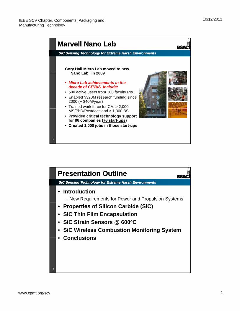
Marvell Nano LabMarvell Nano Lab
Cory Hall Micro Lab moved to new “Nano Lab” in 2009Nano Lab in 2009
• Micro Lab achievements in the decade of CITRIS include:
• 500 active users from 100 faculty PIs• Enabled $320M research funding since
2000 (~ $40M/year)• Trained work force for CA: > 2,000 ,
MS/PhD/Postdocs and > 1,300 BS• Provided critical technology support
for 86 companies (76 start-ups)• Created 1,000 jobs in those start-ups
3
SiCSiC Sensing Technology for Extreme Sensing Technology for Extreme Harsh EnvironmentsHarsh Environments
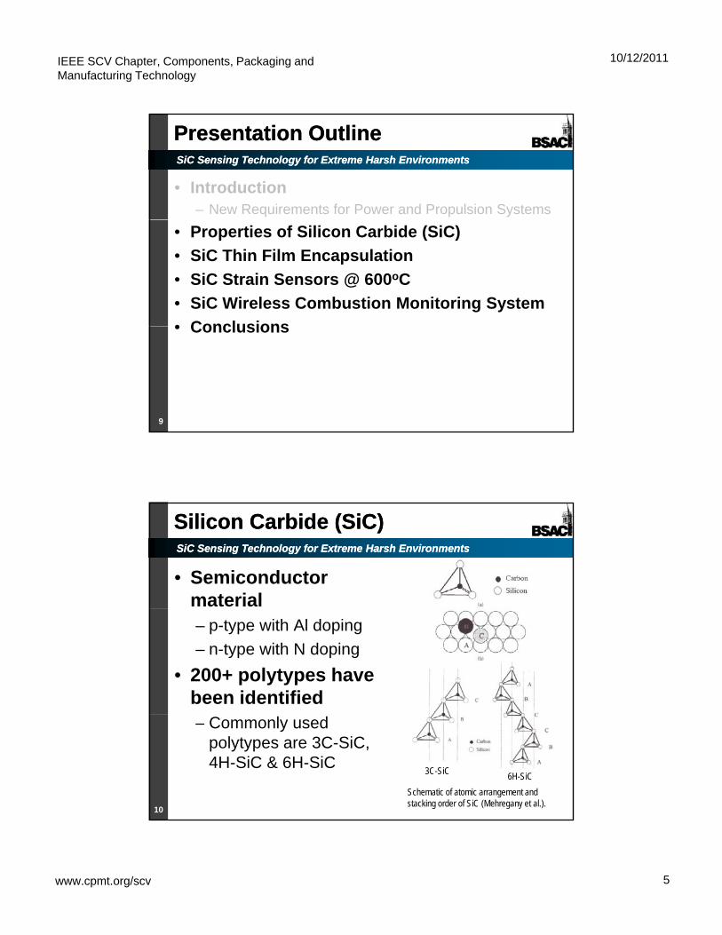
Presentation OutlinePresentation Outline
• Introduction– New Requirements for Power and Propulsion Systems
• Properties of Silicon Carbide (SiC)
• SiC Thin Film Encapsulation
• SiC Strain Sensors @ 600oC
• SiC Wireless Combustion Monitoring System
• Conclusions• Conclusions
4
IEEE SCV Chapter, Components, Packaging and Manufacturing Technology
10/12/2011
www.cpmt.org/scv 3
SiCSiC Sensing Technology for Extreme Sensing Technology for Extreme Harsh EnvironmentsHarsh Environments
IntroductionIntroduction
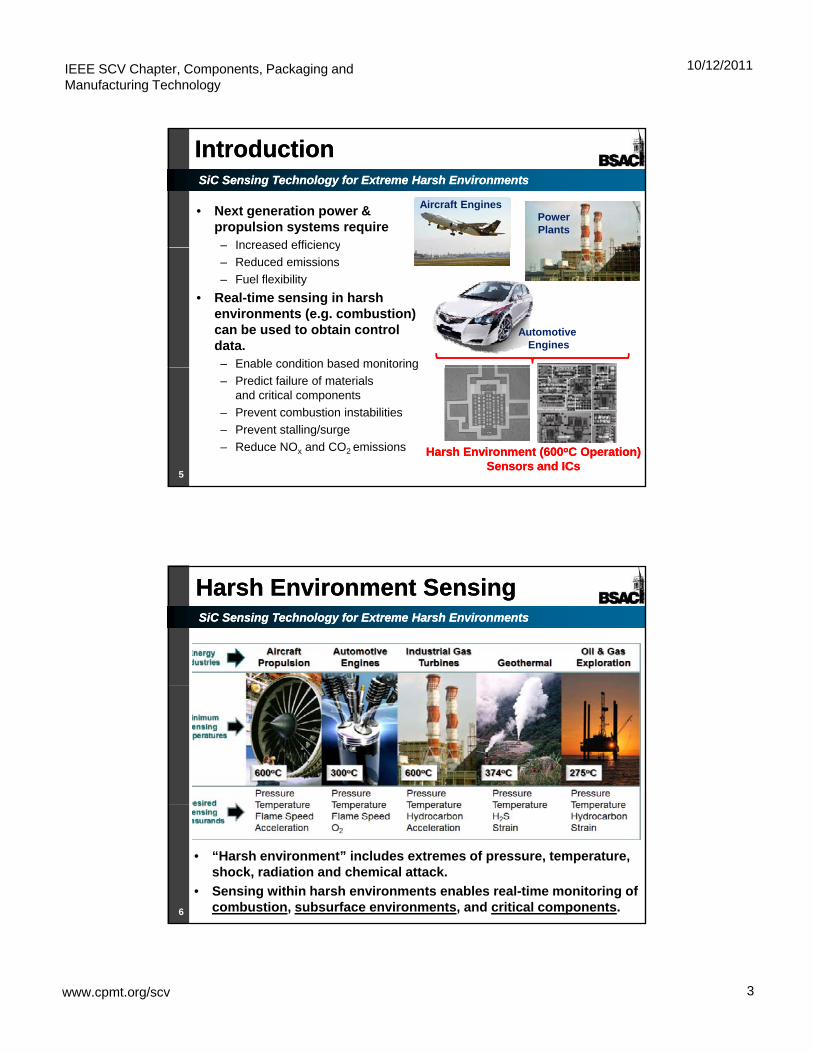
• Next generation power & propulsion systems require– Increased efficiency
Aircraft EnginesPower Plants
Increased efficiency
– Reduced emissions
– Fuel flexibility
• Real-time sensing in harsh environments (e.g. combustion) can be used to obtain control data.– Enable condition based monitoring
AutomotiveEngines
Enable condition based monitoring
– Predict failure of materialsand critical components
– Prevent combustion instabilities
– Prevent stalling/surge
– Reduce NOx and CO2 emissions
5
Harsh Environment (600Harsh Environment (600ooC Operation) C Operation) Sensors and ICsSensors and ICs
SiCSiC Sensing Technology for Extreme Sensing Technology for Extreme Harsh EnvironmentsHarsh Environments
Harsh Environment SensingHarsh Environment Sensing
• “Harsh environment” includes extremes of pressure, temperature, shock, radiation and chemical attack.
• Sensing within harsh environments enables real-time monitoring of combustion, subsurface environments, and critical components. 6
IEEE SCV Chapter, Components, Packaging and Manufacturing Technology
10/12/2011
www.cpmt.org/scv 4
SiCSiC Sensing Technology for Extreme Sensing Technology for Extreme Harsh EnvironmentsHarsh Environments
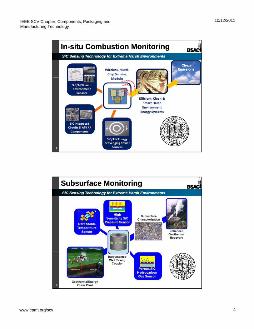
InIn--situ Combustion Monitoringsitu Combustion Monitoring
Clean Clean EmissionsEmissions
7
SiCSiC Sensing Technology for Extreme Sensing Technology for Extreme Harsh EnvironmentsHarsh Environments
Subsurface MonitoringSubsurface Monitoring
8
IEEE SCV Chapter, Components, Packaging and Manufacturing Technology
10/12/2011
www.cpmt.org/scv 5
SiCSiC Sensing Technology for Extreme Sensing Technology for Extreme Harsh EnvironmentsHarsh Environments
Presentation OutlinePresentation Outline
• Introduction– New Requirements for Power and Propulsion Systems
• Properties of Silicon Carbide (SiC)
• SiC Thin Film Encapsulation
• SiC Strain Sensors @ 600oC
• SiC Wireless Combustion Monitoring System
• Conclusions• Conclusions
9
SiCSiC Sensing Technology for Extreme Sensing Technology for Extreme Harsh EnvironmentsHarsh Environments
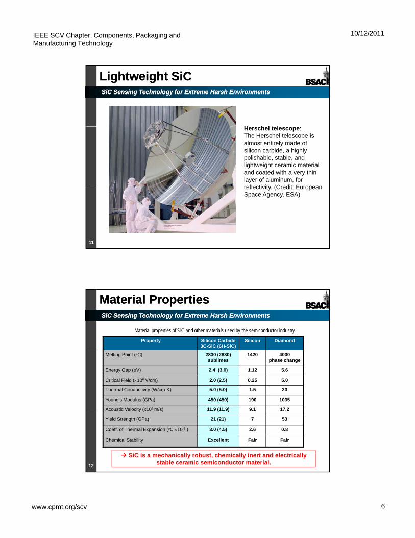
Silicon Carbide (SiC)Silicon Carbide (SiC)
• Semiconductor material– p-type with Al doping
– n-type with N doping
• 200+ polytypes have been identified– Commonly used
polytypes are 3C-SiC, 4H-SiC & 6H-SiC
Schematic of atomic arrangement and stacking order of SiC (Mehregany et al.).
3C-SiC6H-SiC
10
IEEE SCV Chapter, Components, Packaging and Manufacturing Technology
10/12/2011
www.cpmt.org/scv 6
SiCSiC Sensing Technology for Extreme Sensing Technology for Extreme Harsh EnvironmentsHarsh Environments
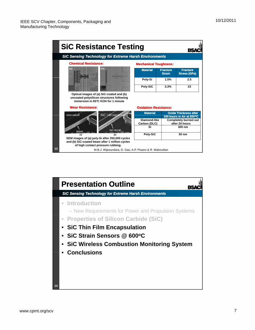
Lightweight Lightweight SiCSiC
H h l t lHerschel telescope:The Herschel telescope is almost entirely made of silicon carbide, a highly polishable, stable, and lightweight ceramic material and coated with a very thin layer of aluminum, for reflectivity (Credit: European
11
reflectivity. (Credit: European Space Agency, ESA)
SiCSiC Sensing Technology for Extreme Sensing Technology for Extreme Harsh EnvironmentsHarsh Environments
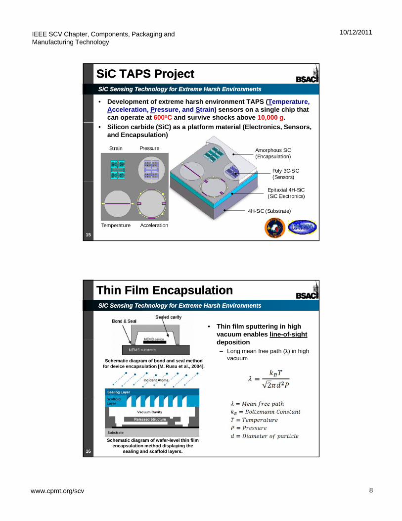
Material PropertiesMaterial Properties
Material properties of SiC and other materials used by the semiconductor industry.
Property Silicon Carbide 3C-SiC (6H-SiC)
Silicon Diamond
Melting Point (oC) 2830 (2830) sublimes
1420 4000phase change
Energy Gap (eV) 2.4 (3.0) 1.12 5.6
Critical Field (106 V/cm) 2.0 (2.5) 0.25 5.0
Thermal Conductivity (W/cm-K) 5.0 (5.0) 1.5 20
Young’s Modulus (GPa) 450 (450) 190 1035
Acoustic Velocity (x103 m/s) 11.9 (11.9) 9.1 17.2
12
y ( ) ( )
Yield Strength (GPa) 21 (21) 7 53
Coeff. of Thermal Expansion (oC 10-6 ) 3.0 (4.5) 2.6 0.8
Chemical Stability Excellent Fair Fair
SiC is a mechanically robust, chemically inert and electrically stable ceramic semiconductor material.
IEEE SCV Chapter, Components, Packaging and Manufacturing Technology
10/12/2011
www.cpmt.org/scv 7
SiCSiC Sensing Technology for Extreme Sensing Technology for Extreme Harsh EnvironmentsHarsh Environments
SiCSiC Resistance TestingResistance Testing
MaterialMaterial Fracture Fracture
StrainStrainFracture Fracture
Stress Stress (GPa)(GPa)
Chemical Resistance:Chemical Resistance: Mechanical Toughness:Mechanical Toughness:
Optical images of (a) SiC-coated and (b) uncoated polysilicon structures following
immersion in 65ºC KOH for 1 minute
MaterialMaterial Oxide Thickness after Oxide Thickness after
Poly-Si 1.5% 2.5
Poly-SiC 3.3% 23
Wear Resistance:Wear Resistance: Oxidation Resistance:Oxidation Resistance:
13
100 hours in Air at 850100 hours in Air at 850OOCCDiamond-like
Carbon (DLC)Completely burned out
after 24 hoursSi 300 nm
Poly-SiC 50 nmSEM images of (a) poly-Si after 250,000 cycles and (b) SiC-coated beam after 1 million cycles
of high contact pressure rubbing.
M.B.J. Wijesundara, D. Gao, A.P. Pisano & R. Maboudian
SiCSiC Sensing Technology for Extreme Sensing Technology for Extreme Harsh EnvironmentsHarsh Environments
Presentation OutlinePresentation Outline
• Introduction– New Requirements for Power and Propulsion Systems
• Properties of Silicon Carbide (SiC)
• SiC Thin Film Encapsulation
• SiC Strain Sensors @ 600oC
• SiC Wireless Combustion Monitoring System
• Conclusions• Conclusions
14
IEEE SCV Chapter, Components, Packaging and Manufacturing Technology
10/12/2011
www.cpmt.org/scv 8
SiCSiC Sensing Technology for Extreme Sensing Technology for Extreme Harsh EnvironmentsHarsh Environments
SiCSiC TAPS ProjectTAPS Project
• Development of extreme harsh environment TAPS (Temperature, Acceleration, Pressure, and Strain) sensors on a single chip that can operate at 600oC and survive shocks above 10,000 g.
Amorphous SiC (Encapsulation)
Poly 3C-SiC (Sensors)
PressureStrain
• Silicon carbide (SiC) as a platform material (Electronics, Sensors, and Encapsulation)
Epitaxial 4H-SiC (SiC Electronics)
4H-SiC (Substrate)
Temperature Acceleration
15
SiCSiC Sensing Technology for Extreme Sensing Technology for Extreme Harsh EnvironmentsHarsh Environments
Thin Film EncapsulationThin Film Encapsulation
• Thin film sputtering in high vacuum enables line-of-sightdeposition – Long mean free path (λ) in high
vacuum Schematic diagram of bond and seal method for device encapsulation [M. Rusu et al., 2004].
Schematic diagram of wafer-level thin film encapsulation method displaying the
sealing and scaffold layers.16
IEEE SCV Chapter, Components, Packaging and Manufacturing Technology
10/12/2011
www.cpmt.org/scv 9
SiCSiC Sensing Technology for Extreme Sensing Technology for Extreme Harsh EnvironmentsHarsh Environments
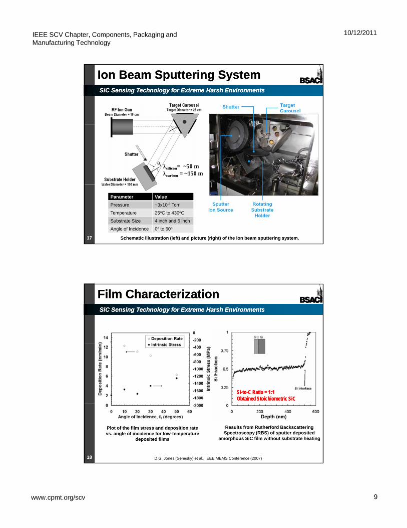
Ion Beam Sputtering SystemIon Beam Sputtering System
λsilicon= ~50 mλcarbon = ~150 m
Schematic illustration (left) and picture (right) of the ion beam sputtering system.
Parameter Value
Pressure ~3x10⁻⁶ Torr
Temperature 25oC to 430oC
Substrate Size 4 inch and 6 inch
Angle of Incidence 0o to 60o
17
SiCSiC Sensing Technology for Extreme Sensing Technology for Extreme Harsh EnvironmentsHarsh Environments
Film Characterization Film Characterization
SiSi--toto--C Ratio = 1:1 C Ratio = 1:1 Obtained Obtained StoichiometricStoichiometric SiCSiC
Plot of the film stress and deposition rate vs. angle of incidence for low-temperature
deposited films
Results from Rutherford Backscattering Spectroscopy (RBS) of sputter deposited
amorphous SiC film without substrate heating
D.G. Jones (Senesky) et al., IEEE MEMS Conference (2007)18
IEEE SCV Chapter, Components, Packaging and Manufacturing Technology
10/12/2011
www.cpmt.org/scv 10
SiCSiC Sensing Technology for Extreme Sensing Technology for Extreme Harsh EnvironmentsHarsh Environments
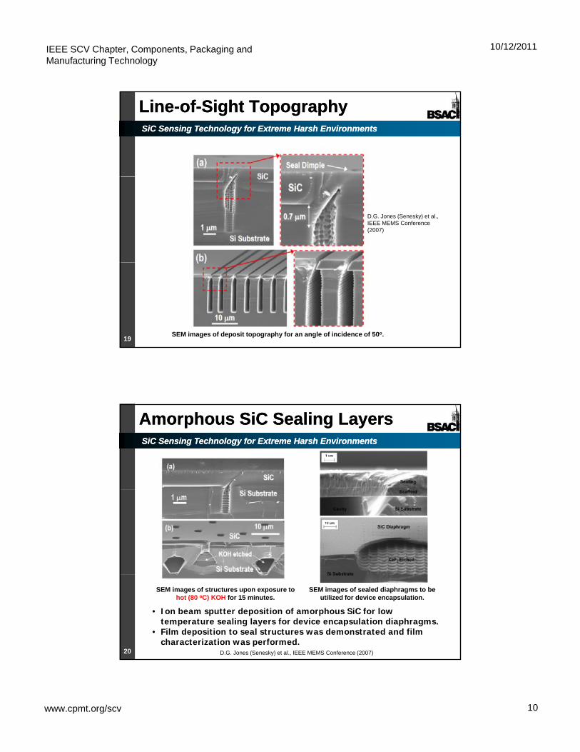
LineLine--ofof--Sight TopographySight Topography
D.G. Jones (Senesky) et al., IEEE MEMS Conference (2007)
SEM images of deposit topography for an angle of incidence of 50o.19
SiCSiC Sensing Technology for Extreme Sensing Technology for Extreme Harsh EnvironmentsHarsh Environments
Amorphous Amorphous SiCSiC Sealing LayersSealing Layers
20
• Ion beam sputter deposition of amorphous SiC for low temperature sealing layers for device encapsulation diaphragms.
• Film deposition to seal structures was demonstrated and film characterization was performed.
SEM images of sealed diaphragms to be utilized for device encapsulation.
SEM images of structures upon exposure to hot (80 oC) KOH for 15 minutes.
D.G. Jones (Senesky) et al., IEEE MEMS Conference (2007)
IEEE SCV Chapter, Components, Packaging and Manufacturing Technology
10/12/2011
www.cpmt.org/scv 11
SiCSiC Sensing Technology for Extreme Sensing Technology for Extreme Harsh EnvironmentsHarsh Environments
Presentation OutlinePresentation Outline
• Introduction– New Requirements for Power and Propulsion Systems
• Properties of Silicon Carbide (SiC)
• SiC Thin Film Encapsulation
• SiC Strain Sensors @ 600oC
• SiC Wireless Combustion Monitoring System
• Conclusions• Conclusions
21
SiCSiC Sensing Technology for Extreme Sensing Technology for Extreme Harsh EnvironmentsHarsh Environments
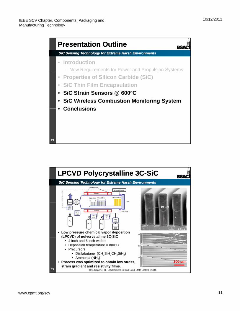
LPCVD Polycrystalline 3CLPCVD Polycrystalline 3C--SiCSiC
• Low pressure chemical vapor deposition (LPCVD) of polycrystalline 3C-SiC
22
( C ) o po yc ysta e 3C S C• 4 inch and 6 inch wafers• Deposition temperature = 800oC• Precursors
• Disilabutane (CH3SiH2CH2SiH3)• Ammonia (NH3)
• Process was optimized to obtain low stress, strain gradient and resistivity films.
C.S. Roper et al., Electrochemical and Solid-State Letters (2008)
200 µm
IEEE SCV Chapter, Components, Packaging and Manufacturing Technology
10/12/2011
www.cpmt.org/scv 12
SiCSiC Sensing Technology for Extreme Sensing Technology for Extreme Harsh EnvironmentsHarsh Environments
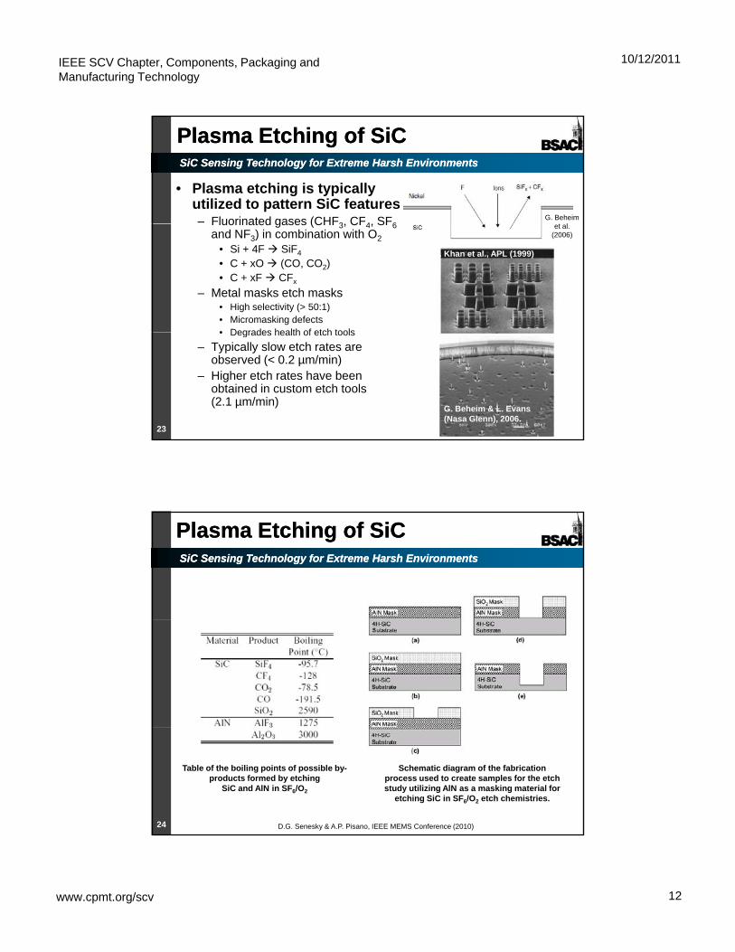
Plasma Etching of Plasma Etching of SiCSiC
• Plasma etching is typically utilized to pattern SiC features– Fluorinated gases (CHF3 CF4 SF6
G. Beheim t lFluorinated gases (CHF3, CF4, SF6
and NF3) in combination with O2
• Si + 4F SiF4
• C + xO (CO, CO2)• C + xF CFx
– Metal masks etch masks • High selectivity (> 50:1)• Micromasking defects• Degrades health of etch tools
E. Khan et al., APL (1999)
et al. (2006)
• Degrades health of etch tools
– Typically slow etch rates are observed (< 0.2 µm/min)
– Higher etch rates have been obtained in custom etch tools (2.1 µm/min)
G. Beheim & L. Evans (Nasa Glenn), 2006.
23
SiCSiC Sensing Technology for Extreme Sensing Technology for Extreme Harsh EnvironmentsHarsh Environments
Plasma Etching of Plasma Etching of SiCSiC
Table of the boiling points of possible by-products formed by etching
SiC and AlN in SF6/O2
D.G. Senesky & A.P. Pisano, IEEE MEMS Conference (2010)
Schematic diagram of the fabricationprocess used to create samples for the etch study utilizing AlN as a masking material for
etching SiC in SF6/O2 etch chemistries.
24
IEEE SCV Chapter, Components, Packaging and Manufacturing Technology
10/12/2011
www.cpmt.org/scv 13
SiCSiC Sensing Technology for Extreme Sensing Technology for Extreme Harsh EnvironmentsHarsh Environments
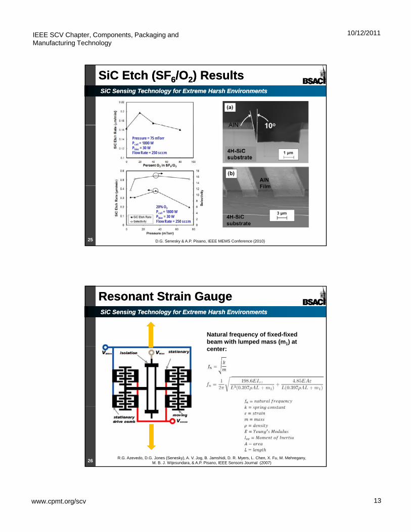
SiC Etch (SFSiC Etch (SF66/O/O22) Results) Results
Pressure = 75 mTorrPcoil = 1800 WPbias = 30 WFlow Rate = 250 sccm
20% O2
Pcoil = 1800 WPbias = 30 WFlow Rate = 250 sccm
D.G. Senesky & A.P. Pisano, IEEE MEMS Conference (2010)25
SiCSiC Sensing Technology for Extreme Sensing Technology for Extreme Harsh EnvironmentsHarsh Environments
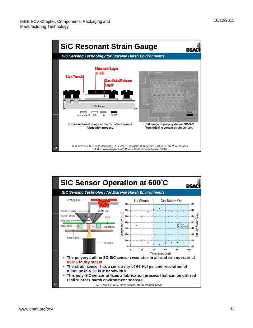
Resonant Strain GaugeResonant Strain Gauge
Natural frequency of fixed-fixed beam with lumped mass (m1) at center:
26R.G. Azevedo, D.G. Jones (Senesky), A. V. Jog, B. Jamshidi, D. R. Myers, L. Chen, X. Fu, M. Mehregany,
M. B. J. Wijesundara, & A.P. Pisano, IEEE Sensors Journal (2007)
IEEE SCV Chapter, Components, Packaging and Manufacturing Technology
10/12/2011
www.cpmt.org/scv 14
SiCSiC Sensing Technology for Extreme Sensing Technology for Extreme Harsh EnvironmentsHarsh Environments
SiCSiC Resonant Strain GaugeResonant Strain Gauge
Etch TrenchEtch Trench
Structural LayerStructural Layer3C3C--SiCSiC
Etch TrenchEtch TrenchSacrificial/Release Sacrificial/Release LayerLayer
27
SEM image of polycrystalline 3C-SiC (7um thick) resonant strain sensor.
Cross-sectional image of the SiC strain sensor fabrication process.
R.G. Azevedo, D.G. Jones (Senesky), A. V. Jog, B. Jamshidi, D. R. Myers, L. Chen, X. Fu, M. Mehregany, M. B. J. Wijesundara, & A.P. Pisano, IEEE Sensors Journal (2007)
SiCSiC Sensing Technology for Extreme Sensing Technology for Extreme Harsh EnvironmentsHarsh Environments
SiC Sensor Operation at 600SiC Sensor Operation at 600ººCC
28
• The polycrystalline 3C-SiC sensor resonates in air and can operate at 600°C in dry steam
• The strain sensor has a sensitivity of 66 Hz/µε and resolution of 0.045 µε in a 10 kHz bandwidth
• This poly-SiC sensor utilizes a fabrication process that can be utilized realize other harsh environment sensors.
D. R. Myers et al., J. Micro/Nanolith. MEMS MOEMS (2009)
IEEE SCV Chapter, Components, Packaging and Manufacturing Technology
10/12/2011
www.cpmt.org/scv 15
SiCSiC Sensing Technology for Extreme Sensing Technology for Extreme Harsh EnvironmentsHarsh Environments
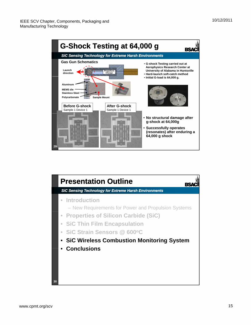
GG--Shock Testing at 64,000 gShock Testing at 64,000 g
• G-shock Testing carried out at Aerophysics Research Center at University of Alabama in Huntsville
• Hard-launch soft-catch method I i i l G l d i 64 000
Launch direction
Gas Gun Schematics
• Initial G-load is 64,000 g.
MEMS dieStainless Steel
Aluminum
Sample MountPolycarbonate
Before G-shockSample 1 Device 1
After G-shockSample 1 Device 1
• No structural damage after g-shock at 64,000g
• Successfully operates (resonates) after enduring a 64,000 g shock
29
SiCSiC Sensing Technology for Extreme Sensing Technology for Extreme Harsh EnvironmentsHarsh Environments
Presentation OutlinePresentation Outline
• Introduction– New Requirements for Power and Propulsion Systems
• Properties of Silicon Carbide (SiC)
• SiC Thin Film Encapsulation
• SiC Strain Sensors @ 600oC
• SiC Wireless Combustion Monitoring System
• Conclusions• Conclusions
30
IEEE SCV Chapter, Components, Packaging and Manufacturing Technology
10/12/2011
www.cpmt.org/scv 16
SiCSiC Sensing Technology for Extreme Sensing Technology for Extreme Harsh EnvironmentsHarsh Environments
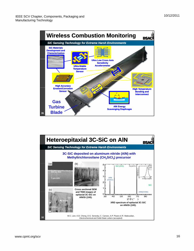
Wireless Combustion MonitoringWireless Combustion Monitoring
SiCSiC Materials Materials Development and Development and CharacterizationCharacterization
High Accuracy High Accuracy
Ultra Low Cross Axis Ultra Low Cross Axis Sensitivity Sensitivity
AccelerometerAccelerometerUltraUltra--Stable Stable Temperature Temperature
SensorSensor
High Temperature High Temperature Bonding and Bonding and InterconnectInterconnect
AlNAlN Energy Energy Scavenging DiaphragmScavenging Diaphragm
Erosion/Corrosion Erosion/Corrosion SensorSensor
3131
Gas Gas Turbine Turbine BladeBlade
SiCSiC Sensing Technology for Extreme Sensing Technology for Extreme Harsh EnvironmentsHarsh Environments
HeteroepitaxialHeteroepitaxial 3C3C--SiC on SiC on AlNAlN
3C-SiC deposited on aluminum nitride (AlN) with Methyltrichlorosilane (CH3SiCl3) precursor
Cross sectional SEM and TEM images of
32
and TEM images of epitaxial 3C-SiC on
AlN/Si (100).
XRD spectrum of epitaxial 3C-SiC on AlN/Si (100).
W.C. Lien, K.B. Cheng, D.G. Senesky, C. Carraro, A.P. Pisano & R. Maboudian, Electrochemical and Solid-State Letters (accepted)
IEEE SCV Chapter, Components, Packaging and Manufacturing Technology
10/12/2011
www.cpmt.org/scv 17
SiCSiC Sensing Technology for Extreme Sensing Technology for Extreme Harsh EnvironmentsHarsh Environments
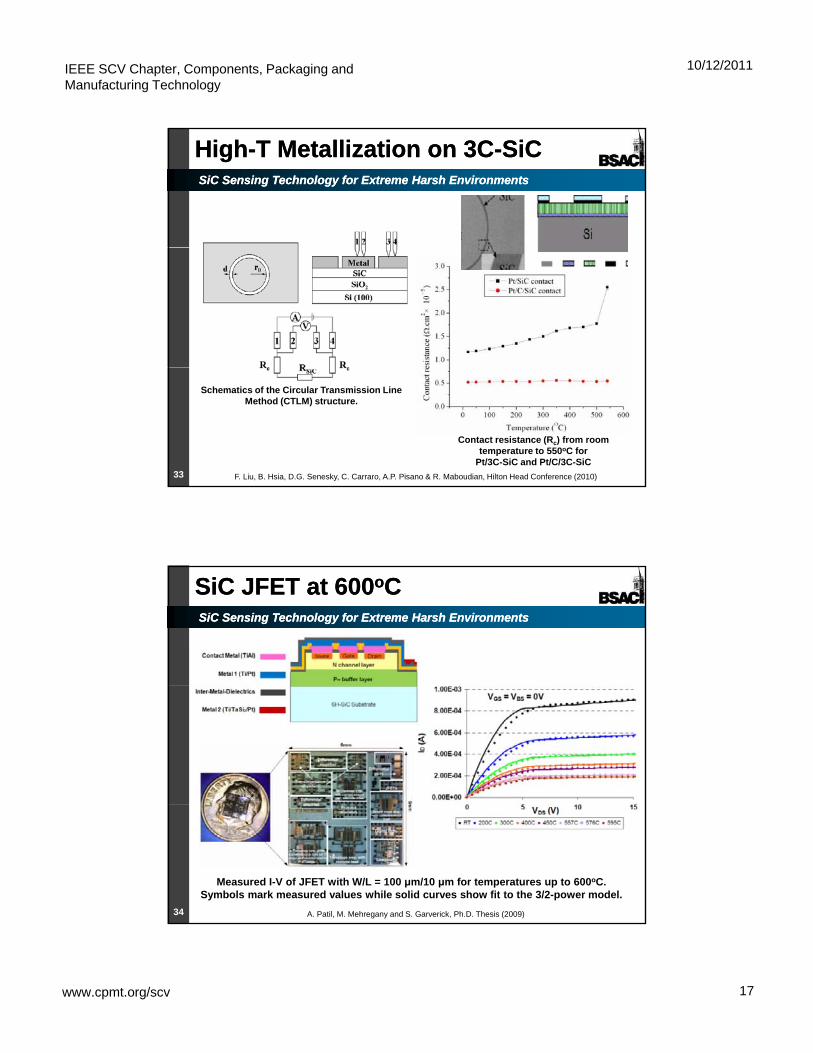
HighHigh--T Metallization on 3CT Metallization on 3C--SiCSiC
33
Schematics of the Circular Transmission Line Method (CTLM) structure.
Contact resistance (Rc) from room temperature to 550oC for
Pt/3C-SiC and Pt/C/3C-SiC
F. Liu, B. Hsia, D.G. Senesky, C. Carraro, A.P. Pisano & R. Maboudian, Hilton Head Conference (2010)
SiCSiC Sensing Technology for Extreme Sensing Technology for Extreme Harsh EnvironmentsHarsh Environments
SiC JFET at 600SiC JFET at 600ooCC
34
Measured I-V of JFET with W/L = 100 μm/10 μm for temperatures up to 600oC. Symbols mark measured values while solid curves show fit to the 3/2-power model.
A. Patil, M. Mehregany and S. Garverick, Ph.D. Thesis (2009)
IEEE SCV Chapter, Components, Packaging and Manufacturing Technology
10/12/2011
www.cpmt.org/scv 18
SiCSiC Sensing Technology for Extreme Sensing Technology for Extreme Harsh EnvironmentsHarsh Environments
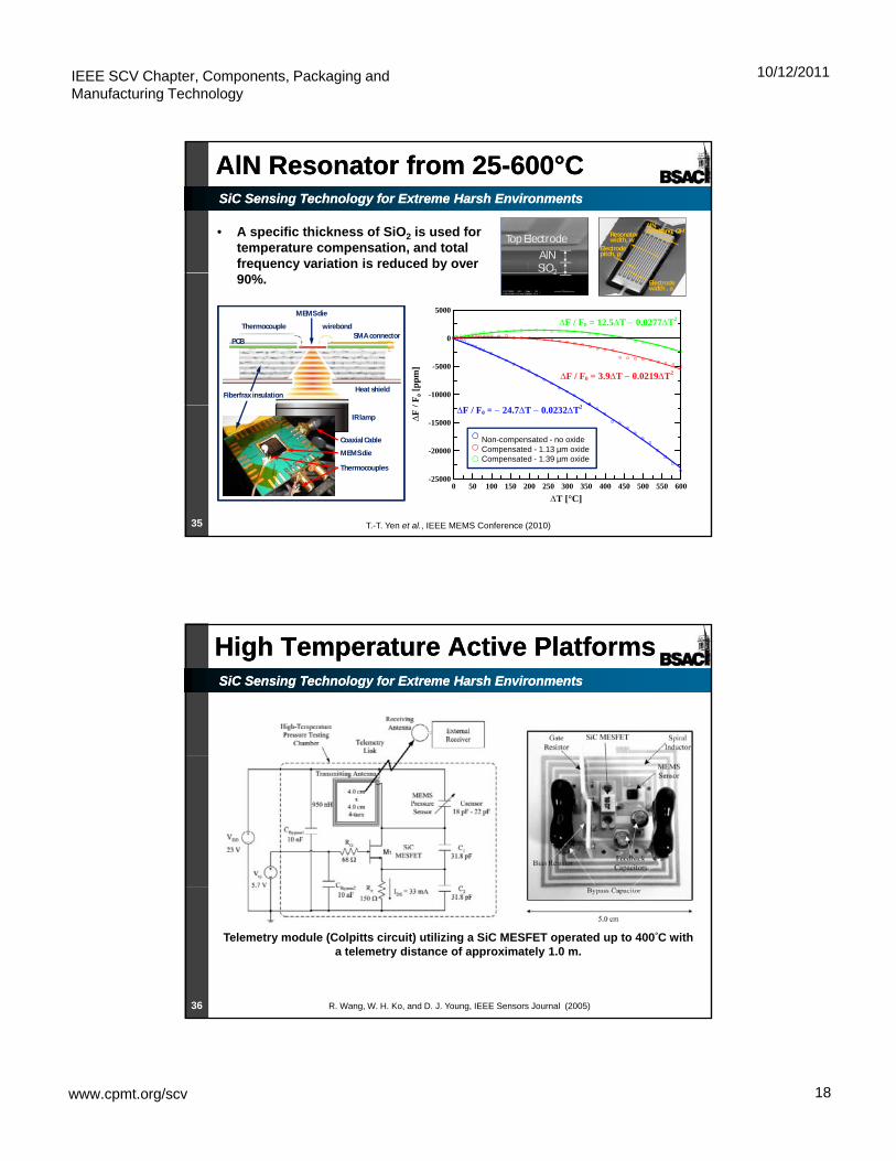
AlNAlN Resonator from 25Resonator from 25--600600°°CC
• A specific thickness of SiO2 is used for temperature compensation, and total frequency variation is reduced by over
Top Electrode
AlNSiO2
Top Electrode
AlNoverhang, OH
Resonator width, w
Electrode pitch, p
90%.
Heat shieldFiberfrax insulation
MEMS die
wirebondThermocouple
PCBSMA connector
Heat shieldFiberfrax insulation
MEMS die
wirebondThermocouple
PCBSMA connector
-10000
-5000
0
5000
/ F0 [
ppm
]2
F / F0 = 12.5T 0.0277T2
F / F0 = 3.9T 0.0219T2
2
Electrode width , a
IR lamp
MEMS die
Thermocouples
Coaxial Cable
IR lamp
MEMS die
Thermocouples
Coaxial Cable
0 50 100 150 200 250 300 350 400 450 500 550 600
T [°C]
-25000
-20000
-15000F /
F / F0 = 24.7T 0.0232T2
Non-compensated - no oxideCompensated - 1.13 µm oxideCompensated - 1.39 µm oxide
35 T.-T. Yen et al., IEEE MEMS Conference (2010)
SiCSiC Sensing Technology for Extreme Sensing Technology for Extreme Harsh EnvironmentsHarsh Environments
High Temperature Active PlatformsHigh Temperature Active Platforms
36 R. Wang, W. H. Ko, and D. J. Young, IEEE Sensors Journal (2005)
Telemetry module (Colpitts circuit) utilizing a SiC MESFET operated up to 400°C with a telemetry distance of approximately 1.0 m.
IEEE SCV Chapter, Components, Packaging and Manufacturing Technology
10/12/2011
www.cpmt.org/scv 19
SiCSiC Sensing Technology for Extreme Sensing Technology for Extreme Harsh EnvironmentsHarsh Environments
ConclusionsConclusions
• Advanced power and propulsion systems (e.g. aircraft propulsion, industrial gas turbines and p p , gautomotive engines) can utilize robust sensors for increased fuel efficiency, increased operation lifetimes and reduced emissions.
• Development of advanced ceramic semiconductors (materials & processes) has enabled a new class of sensors and electronics that can operate in hostile
37
pconditions.
• Future research includes systems integration to realize a wireless sensing module. This will require novel packaging and interconnect technology.
SiCSiC Sensing Technology for Extreme Sensing Technology for Extreme Harsh EnvironmentsHarsh Environments
AcknowledgementsAcknowledgements
UCB Faculty and Alumni:
• Prof Albert P Pisano
UCB Post Docs & GSRs:
• Dr Ayden MaralaniProf. Albert P. Pisano
• Prof. Roya Maboudian
• Dr. Muthu Wijesundara
• Dr. Robert Azevedo
• Dr. Chris Roper
• Dr. Babak Jamshidi
Dr. Ayden Maralani
• Dr. Mohammad Shavezipur
• Dr. Maxime Vincent
• Mr. Ting-ta Yen
• Mr. Benjamin Cheng
• Mr. Matt Chan
• Dr. David Myers
Case Western Faculty:
• Prof. Mehran Mehregany
• Prof. Steve Garverick
• Ms. Sarah Wodin-Schwartz
• Ms. Matilda Lai
• Mr. Wei-Cheng Lien
• Ms. Kirti Mansukhani38