SigmaDSP Digital Audio Processor Data Sheet … · 2019-06-05 · SigmaDSP Digital Audio Processor...
202
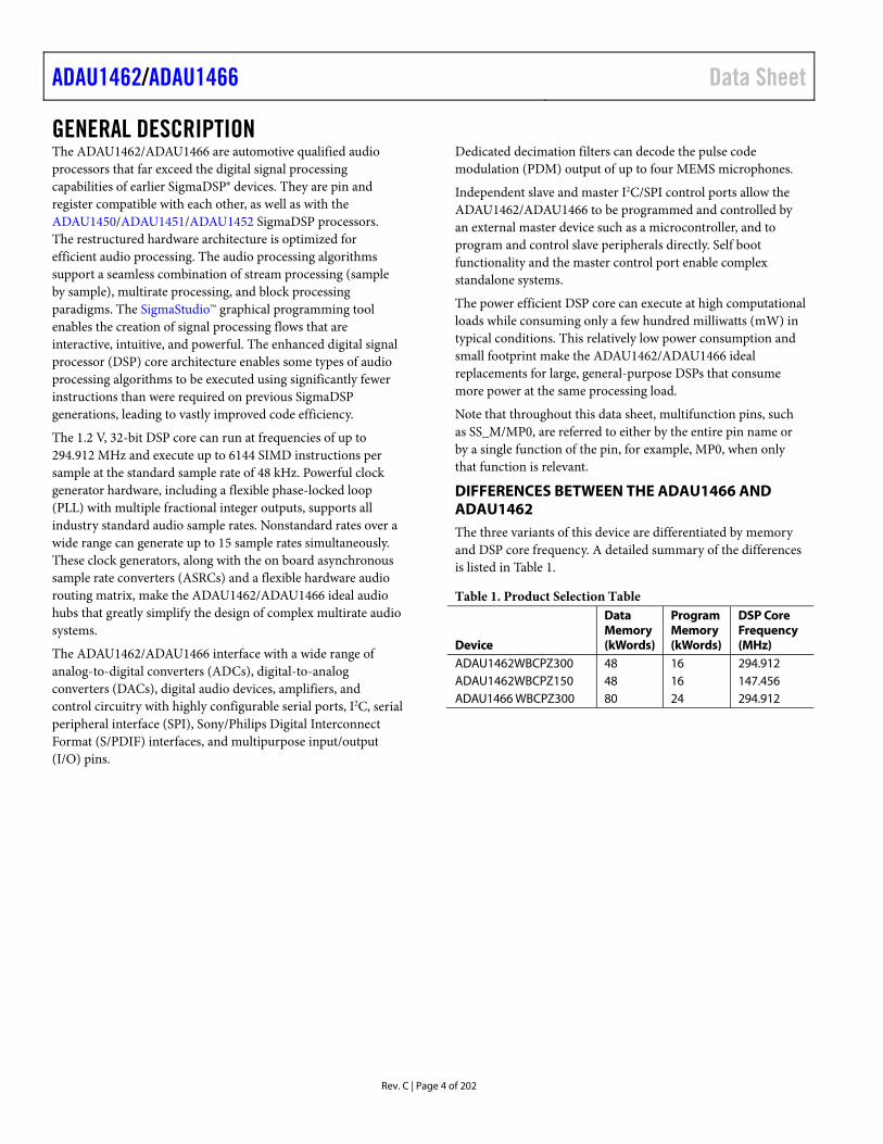
SigmaDSP Digital Audio Processor Data Sheet ADAU1462/ADAU1466 Rev. C Document Feedback Information furnished by Analog Devices is believed to be accurate and reliable. However, no responsibility is assumed by Analog Devices for its use, nor for any infringements of patents or other rights of third parties that may result from its use. Specifications subject to change without notice. No license is granted by implication or otherwise under any patent or patent rights of Analog Devices. Trademarks and registered trademarks are the property of their respective owners. One Technology Way, P.O. Box 9106, Norwood, MA 02062-9106, U.S.A. Tel: 781.329.4700 ©2017–2018 Analog Devices, Inc. All rights reserved. Technical Support www.analog.com FEATURES Qualified for automotive applications Fully programmable audio DSP for enhanced sound processing Features SigmaStudio, a proprietary graphical programming tool for the development of custom signal flows Up to 294.912 MHz, 32-bit SigmaDSP core at 1.2 V Up to 24 kWords of program memory Up to 80 kWords of parameter/data RAM Up to 6144 SIMD instructions per sample at 48 kHz Up to 1600 ms digital audio delay pool at 48 kHz Audio I/O and routing 4 serial input ports, 4 serial output ports 48-channel, 32-bit digital I/O up to a sample rate of 192 kHz Flexible configuration for TDM, I 2 S, left and right justified formats, and PCM Up to 8 stereo ASRCs from 1:8 up to 7.75:1 ratio and 139 dB dynamic range Stereo S/PDIF input and output at 192 kHz Four PDM microphone input channels Multichannel, byte addressable TDM serial ports Clock oscillator for generating master clock from crystal Integer PLL and flexible clock generators Integrated die temperature sensor I 2 C and SPI control interfaces (both slave and master) Standalone operation Self-boot from serial EEPROM 6-channel, 10-bit SAR auxiliary control ADC 14 multipurpose pins for digital controls and outputs On-chip regulator for generating 1.2 V from 3.3 V supply 72-lead, 10 mm × 10 mm LFCSP package with 5.3 mm exposed pad Temperature range: −40°C to +105°C APPLICATIONS Automotive audio processing Head units Distributed amplifiers Rear seat entertainment systems Trunk amplifiers Commercial and professional audio processing FUNCTIONAL BLOCK DIAGRAM S/PDIF TRANSMITTER S/PDIF RECEIVER 8 × 2-CHANNEL ASYNCHRONOUS SAMPLE RATE CONVERTERS INPUT CLOCK DOMAINS (×4) OUTPUT CLOCK DOMAINS (×4) CLOCK OSCILLATOR GPIO/ AUX ADC PLL I 2 C/SPI SLAVE XTALIN/MCLK XTALOUT SPI/I 2 C* BCLK_IN3 TO BCLK_IN0/ LRCLK_IN3 TO LRCLK_IN0 (INPUT CLOCK PAIRS) SELFBOOT SPDIFIN SPDIFOUT CLKOUT SDATA_IN3 TO SDATA_IN0 (48-CHANNEL DIGITAL AUDIO INPUTS) SDATA_OUT3 TO SDATA_OUT0 (48-CHANNEL DIGITAL AUDIO OUTPUTS) REGULATOR ADAU1462/ ADAU1466 PLLFILT MP13 TO MP0 AUXADC5 TO AUXADC0 BCLK_OUT3 TO BCLK_OUT0 LRCLK_OUT3 TO LRCLK_OUT0 (OUTPUT CLOCK PAIRS) TEMPERATURE SENSOR THD_P VDRIVE THD_M I 2 C/SPI MASTER SPI/I 2 C* DIGITAL MIC INPUT SERIAL DATA INPUT PORTS (×4) SERIAL DATA OUTPUT PORTS (×4) DEJITTER AND CLOCK GENERATOR INPUT AUDIO ROUTING MATRIX OUTPUT AUDIO ROUTING MATRIX 294.912MHz PROGRAMMABLE AUDIO PROCESSING CORE RAM, ROM, WATCHDOG, MEMORY PARITY CHECK 14810-001 *SPI/I 2 C INCLUDES THE FOLLOWING PIN FUNCTIONS: SS_M, MOSI_M, SCL_M, SCLK_M, SDA_M, MISO_M, MISO, SDA, SCLK, SCL, MOSI, ADDR1, SS, AND ADDR0 PINS. ® Figure 1.
Transcript of SigmaDSP Digital Audio Processor Data Sheet … · 2019-06-05 · SigmaDSP Digital Audio Processor...
SigmaDSP Digital Audio ProcessorData Sheet ADAU1462/ADAU1466
Rev. C Document Feedback Information furnished by Analog Devices is believed to be accurate and reliable. However, no responsibility is assumed by Analog Devices for its use, nor for any infringements of patents or other rights of third parties that may result from its use. Specifications subject to change without notice. No license is granted by implication or otherwise under any patent or patent rights of Analog Devices. Trademarks and registered trademarks are the property of their respective owners.
One Technology Way, P.O. Box 9106, Norwood, MA 02062-9106, U.S.A.Tel: 781.329.4700 ©2017–2018 Analog Devices, Inc. All rights reserved. Technical Support www.analog.com
FEATURES Qualified for automotive applications Fully programmable audio DSP for enhanced sound processing Features SigmaStudio, a proprietary graphical programming
tool for the development of custom signal flows Up to 294.912 MHz, 32-bit SigmaDSP core at 1.2 V
Up to 24 kWords of program memory Up to 80 kWords of parameter/data RAM Up to 6144 SIMD instructions per sample at 48 kHz Up to 1600 ms digital audio delay pool at 48 kHz
Audio I/O and routing 4 serial input ports, 4 serial output ports 48-channel, 32-bit digital I/O up to a sample rate of 192 kHz Flexible configuration for TDM, I2S, left and right justified
formats, and PCM Up to 8 stereo ASRCs from 1:8 up to 7.75:1 ratio and
139 dB dynamic range Stereo S/PDIF input and output at 192 kHz Four PDM microphone input channels Multichannel, byte addressable TDM serial ports
Clock oscillator for generating master clock from crystal Integer PLL and flexible clock generators Integrated die temperature sensor I2C and SPI control interfaces (both slave and master) Standalone operation
Self-boot from serial EEPROM 6-channel, 10-bit SAR auxiliary control ADC 14 multipurpose pins for digital controls and outputs
On-chip regulator for generating 1.2 V from 3.3 V supply 72-lead, 10 mm × 10 mm LFCSP package with 5.3 mm
exposed pad Temperature range: −40°C to +105°C
APPLICATIONS Automotive audio processing
Head units Distributed amplifiers Rear seat entertainment systems Trunk amplifiers
Commercial and professional audio processing
FUNCTIONAL BLOCK DIAGRAM
S/PDIFTRANSMITTER
S/PDIFRECEIVER
8 × 2-CHANNELASYNCHRONOUS
SAMPLE RATECONVERTERS
INPUTCLOCK
DOMAINS(×4)
OUTPUTCLOCK
DOMAINS(×4)
CLOCKOSCILLATOR
GPIO/AUX ADC PLL
I2C/SPISLAVE
XT
AL
IN/M
CL
K
XT
AL
OU
T
SPI/I2C*
BCLK_IN3 TO BCLK_IN0/LRCLK_IN3 TO LRCLK_IN0
(INPUT CLOCK PAIRS)
SE
LF
BO
OT
SPDIFIN SPDIFOUT
CLKOUT
SDATA_IN3 TO SDATA_IN0(48-CHANNEL
DIGITAL AUDIOINPUTS)
SDATA_OUT3 TO SDATA_OUT0(48-CHANNELDIGITAL AUDIOOUTPUTS)
REGULATOR
ADAU1462/ADAU1466
PLLFILTMP
13 T
O M
P0
AU
XA
DC
5 T
OA
UX
AD
C0
BCLK_OUT3 TO BCLK_OUT0LRCLK_OUT3 TO LRCLK_OUT0(OUTPUT CLOCK PAIRS)
TEMPERATURESENSOR
THD_P
VDRIVE
THD_M
I2C/SPIMASTER
SPI/I2C*
DIGITALMIC INPUT
SERIAL DATAINPUT PORTS
(×4)SERIAL DATA
OUTPUT PORTS(×4)
DEJITTER ANDCLOCK GENERATOR
INPUT AUDIOROUTING MATRIX
OUTPUT AUDIOROUTING MATRIX
294.912MHzPROGRAMMABLE AUDIO
PROCESSING CORE
RAM, ROM, WATCHDOG,MEMORY PARITY CHECK
148
10-0
01
*SPI/I2C INCLUDES THE FOLLOWING PIN FUNCTIONS: SS_M, MOSI_M, SCL_M, SCLK_M, SDA_M, MISO_M, MISO, SDA, SCLK, SCL, MOSI, ADDR1, SS, AND ADDR0 PINS.
®
Figure 1.
ADAU1462/ADAU1466 Data Sheet
Rev. C | Page 2 of 202
TABLE OF CONTENTS Features .............................................................................................. 1
Applications ....................................................................................... 1
Functional Block Diagram .............................................................. 1
Revision History ............................................................................... 3
General Description ......................................................................... 4
Differences Between the ADAU1466 and ADAU1462 ........... 4
Specifications ..................................................................................... 5
Electrical Characteristics ............................................................. 7
Timing Specifications .................................................................. 9
Absolute Maximum Ratings .......................................................... 17
Thermal Considerations ............................................................ 17
ESD Caution ................................................................................ 17
Pin Configuration and Function Descriptions ........................... 18
Theory of Operation ...................................................................... 22
System Block Diagram ............................................................... 22
Overview ...................................................................................... 22
Initialization ................................................................................ 24
Master Clock, PLL, and Clock Generators.............................. 28
Power Supplies, Voltage Regulator, and Hardware Reset ...... 33
Temperature Sensor Diode........................................................ 34
Slave Control Ports ..................................................................... 35
Slave Control Port Addressing .................................................. 35
Slave Port to DSP Core Address Mapping .............................. 36
Master Control Ports .................................................................. 44
Self Boot ....................................................................................... 45
Audio Signal Routing ................................................................. 48
Serial Data Input/Output........................................................... 57
Flexible TDM Interface .............................................................. 68
Asynchronous Sample Rate Converters .................................. 74
S/PDIF Interface ......................................................................... 74
Digital PDM Microphone Interface ......................................... 76
Multipurpose Pins ...................................................................... 77
Auxiliary ADC ............................................................................ 80
SigmaDSP Core .......................................................................... 80
Software Features ....................................................................... 86
Pin Drive Strength, Slew Rate, and Pull Configuration ........ 87
Global RAM and Control Register Map ...................................... 89
Random Access Memory .......................................................... 89
Control Registers ........................................................................ 92
Control Register Details ................................................................ 98
PLL Configuration Registers .................................................... 98
Clock Generator Registers ...................................................... 103
Power Reduction Registers ..................................................... 108
Audio Signal Routing Registers .............................................. 111
Serial Port Configuration Registers ....................................... 117
Flexible TDM Interface Registers ........................................... 121
DSP Core Control Registers .................................................... 124
Debug and Reliability Registers .............................................. 129
Software Panic Value 0 Register ............................................. 136
Software Panic Value 1 Register ............................................. 136
DSP Program Execution Registers ......................................... 139
Panic Mask Registers ............................................................... 142
Multipurpose Pin Configuration Registers........................... 155
ASRC Status and Control Registers ....................................... 160
Auxiliary ADC Registers ......................................................... 164
S/PDIF Interface Registers ...................................................... 165
Hardware Interfacing Registers .............................................. 178
Soft Reset Register .................................................................... 196
Applications Information ............................................................ 197
PCB Design Considerations ................................................... 197
Typical Applications Block Diagram ..................................... 199
Example PCB Layout ............................................................... 200
PCB Manufacturing Guidelines ............................................. 201
Outline Dimensions ..................................................................... 202
Ordering Guide ........................................................................ 202
Automotive Products ............................................................... 202
Data Sheet ADAU1462/ADAU1466
Rev. C | Page 3 of 202
REVISION HISTORY 3/2018—Rev. B to Rev. C Changes to Table 1 ............................................................................ 4 Changes to Table 2 ............................................................................ 5 Changes to Table 3 ............................................................................ 6 Added Endnote 1, Table 6 ................................................................ 9 Deleted Endnote 1, Table 9 ............................................................ 11 Changes to S/PDIF Transmitter and Receiver Section and Table 10 ............................................................................................. 11 Deleted S/PDIF Receiver Section and Table 11; Renumbered Sequentially ...................................................................................... 11 Added Table 11; Renumbered Sequentially ................................. 12 Added I2C Interface—Master Section .......................................... 13 Changes to Table 20 ........................................................................ 29 Changes to Table 21 ........................................................................ 30 Changes to SigmaDSP Core Section ............................................. 80 Changes to Ordering Guide .........................................................202 10/2017—Rev. A to Rev. B Changes to Table 1 ............................................................................ 4 Changes to Table 2 ............................................................................ 5 Changes to Table 3 ............................................................................ 6
Changes to Table 6 ............................................................................ 9 Changes to Table 21 ........................................................................ 29 Changes to PLL Filter Section and Table 22 ................................ 30 Changes to Clock Generators Section and Figure 18 ................. 31 Changes to Figure 19 ...................................................................... 32 Changes to Figure 26 ...................................................................... 37 Changes to Figure 27 ...................................................................... 38 Changes to SigmaDSP Core Section ............................................ 80 Changes to Table 58 ........................................................................ 89 Changes to Figure 82 ...................................................................... 90 Changes to Figure 83 ...................................................................... 91 Changes to Ordering Guide ......................................................... 202 9/2017—Rev. 0 to Rev. A Change to Supply Current Analog Current (AVDD) Parameter, Table 2 ................................................................................................. 4 Change to Supply Current PLL Current (PVDD) Parameter and Supply Current Analog Current (AVDD) Parameter, Table 3 .... 5 Added Endnote 2 to Ordering Guide ......................................... 201 8/2017—Revision 0: Initial Version
ADAU1462/ADAU1466 Data Sheet
Rev. C | Page 4 of 202
GENERAL DESCRIPTION The ADAU1462/ADAU1466 are automotive qualified audio processors that far exceed the digital signal processing capabilities of earlier SigmaDSP® devices. They are pin and register compatible with each other, as well as with the ADAU1450/ADAU1451/ADAU1452 SigmaDSP processors. The restructured hardware architecture is optimized for efficient audio processing. The audio processing algorithms support a seamless combination of stream processing (sample by sample), multirate processing, and block processing paradigms. The SigmaStudio™ graphical programming tool enables the creation of signal processing flows that are interactive, intuitive, and powerful. The enhanced digital signal processor (DSP) core architecture enables some types of audio processing algorithms to be executed using significantly fewer instructions than were required on previous SigmaDSP generations, leading to vastly improved code efficiency.
The 1.2 V, 32-bit DSP core can run at frequencies of up to 294.912 MHz and execute up to 6144 SIMD instructions per sample at the standard sample rate of 48 kHz. Powerful clock generator hardware, including a flexible phase-locked loop (PLL) with multiple fractional integer outputs, supports all industry standard audio sample rates. Nonstandard rates over a wide range can generate up to 15 sample rates simultaneously. These clock generators, along with the on board asynchronous sample rate converters (ASRCs) and a flexible hardware audio routing matrix, make the ADAU1462/ADAU1466 ideal audio hubs that greatly simplify the design of complex multirate audio systems.
The ADAU1462/ADAU1466 interface with a wide range of analog-to-digital converters (ADCs), digital-to-analog converters (DACs), digital audio devices, amplifiers, and control circuitry with highly configurable serial ports, I2C, serial peripheral interface (SPI), Sony/Philips Digital Interconnect Format (S/PDIF) interfaces, and multipurpose input/output (I/O) pins.
Dedicated decimation filters can decode the pulse code modulation (PDM) output of up to four MEMS microphones.
Independent slave and master I2C/SPI control ports allow the ADAU1462/ADAU1466 to be programmed and controlled by an external master device such as a microcontroller, and to program and control slave peripherals directly. Self boot functionality and the master control port enable complex standalone systems.
The power efficient DSP core can execute at high computational loads while consuming only a few hundred milliwatts (mW) in typical conditions. This relatively low power consumption and small footprint make the ADAU1462/ADAU1466 ideal replacements for large, general-purpose DSPs that consume more power at the same processing load.
Note that throughout this data sheet, multifunction pins, such as SS_M/MP0, are referred to either by the entire pin name or by a single function of the pin, for example, MP0, when only that function is relevant.
DIFFERENCES BETWEEN THE ADAU1466 AND ADAU1462 The three variants of this device are differentiated by memory and DSP core frequency. A detailed summary of the differences is listed in Table 1.
Table 1. Product Selection Table
Device
Data Memory (kWords)
Program Memory (kWords)
DSP Core Frequency (MHz)
ADAU1462WBCPZ300 48 16 294.912 ADAU1462WBCPZ150 48 16 147.456 ADAU1466 WBCPZ300 80 24 294.912
Data Sheet ADAU1462/ADAU1466
Rev. C | Page 5 of 202
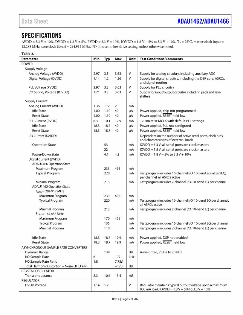
SPECIFICATIONS AVDD = 3.3 V ± 10%, DVDD = 1.2 V ± 5%, PVDD = 3.3 V ± 10%, IOVDD = 1.8 V − 5% to 3.3 V + 10%, TA = 25°C, master clock input = 12.288 MHz, core clock (fCORE) = 294.912 MHz, I/O pins set to low drive setting, unless otherwise noted.
Table 2. Parameter Min Typ Max Unit Test Conditions/Comments POWER
Supply Voltage Analog Voltage (AVDD) 2.97 3.3 3.63 V Supply for analog circuitry, including auxiliary ADC Digital Voltage (DVDD) 1.14 1.2 1.26 V Supply for digital circuitry, including the DSP core, ASRCs,
and signal routing PLL Voltage (PVDD) 2.97 3.3 3.63 V Supply for PLL circuitry I/O Supply Voltage (IOVDD) 1.71 3.3 3.63 V Supply for input/output circuitry, including pads and level
shifters Supply Current
Analog Current (AVDD) 1.36 1.66 2 mA Idle State 1.00 1.10 40 μA Power applied, chip not programmed Reset State 1.00 1.10 40 μA Power applied, RESET held low
PLL Current (PVDD) 8.3 10.1 12.9 mA 12.288 MHz MCLK with default PLL settings Idle State 18.3 18.7 40 μA Power applied, PLL not configured Reset State 18.3 18.7 40 μA Power applied, RESET held low
I/O Current (IOVDD) Dependent on the number of active serial ports, clock pins, and characteristics of external loads
Operation State 53 mA IOVDD = 3.3 V; all serial ports are clock masters 22 mA IOVDD = 1.8 V; all serial ports are clock masters
Power-Down State 4.1 4.2 mA IOVDD = 1.8 V − 5% to 3.3 V + 10% Digital Current (DVDD)
ADAU1466 Operation State Maximum Program 233 495 mA Typical Program 220 mA Test program includes 16-channel I/O, 10-band equalizer (EQ)
per channel, all ASRCs active Minimal Program 213 mA Test program includes 2-channel I/O, 10-band EQ per channel
ADAU1462 Operation State fCORE = 294.912 MHz
Maximum Program 233 495 mA Typical Program 220 mA Test program includes 16-channel I/O, 10-band EQ per channel,
all ASRCs active Minimal Program 213 mA Test program includes 2-channel I/O, 10-band EQ per channel
fCORE = 147.456 MHz Maximum Program 170 455 mA Typical Program 135 mA Test program includes 16-channel I/O, 10-band EQ per channel Minimal Program 110 mA Test program includes 2-channel I/O, 10-band EQ per channel
Idle State 18.3 18.7 19.9 mA Power applied, DSP not enabled Reset State 18.3 18.7 19.9 mA Power applied, RESET held low
ASYNCHRONOUS SAMPLE RATE CONVERTERS Dynamic Range 139 dB A-weighted, 20 Hz to 20 kHz I/O Sample Rate 6 192 kHz I/O Sample Rate Ratio 1:8 7.75:1 Total Harmonic Distortion + Noise (THD + N) −120 dB
CRYSTAL OSCILLATOR Transconductance 8.3 10.6 13.4 mS
REGULATOR DVDD Voltage 1.14 1.2 V Regulator maintains typical output voltage up to a maximum
800 mA load; IOVDD = 1.8 V − 5% to 3.3 V + 10%
ADAU1462/ADAU1466 Data Sheet
Rev. C | Page 6 of 202
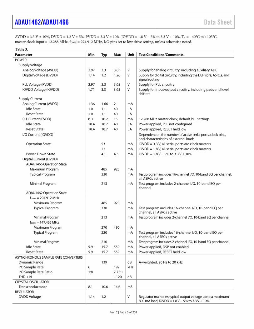
AVDD = 3.3 V ± 10%, DVDD = 1.2 V ± 5%, PVDD = 3.3 V ± 10%, IOVDD = 1.8 V − 5% to 3.3 V + 10%, TA = −40°C to +105°C, master clock input = 12.288 MHz, fCORE = 294.912 MHz, I/O pins set to low drive setting, unless otherwise noted.
Table 3. Parameter Min Typ Max Unit Test Conditions/Comments POWER
Supply Voltage Analog Voltage (AVDD) 2.97 3.3 3.63 V Supply for analog circuitry, including auxiliary ADC Digital Voltage (DVDD) 1.14 1.2 1.26 V Supply for digital circuitry, including the DSP core, ASRCs, and
signal routing PLL Voltage (PVDD) 2.97 3.3 3.63 V Supply for PLL circuitry IOVDD Voltage (IOVDD) 1.71 3.3 3.63 V Supply for input/output circuitry, including pads and level
shifters Supply Current
Analog Current (AVDD) 1.36 1.66 2 mA Idle State 1.0 1.1 40 μA Reset State 1.0 1.1 40 μA
PLL Current (PVDD) 8.3 10.2 15 mA 12.288 MHz master clock; default PLL settings Idle State 18.4 18.7 40 μA Power applied, PLL not configured Reset State 18.4 18.7 40 μA Power applied, RESET held low
I/O Current (IOVDD) Dependent on the number of active serial ports, clock pins, and characteristics of external loads
Operation State 53 mA IOVDD = 3.3 V; all serial ports are clock masters 22 mA IOVDD = 1.8 V; all serial ports are clock masters Power-Down State 4.1 4.3 mA IOVDD = 1.8 V − 5% to 3.3 V + 10%
Digital Current (DVDD) ADAU1466 Operation State
Maximum Program 485 920 mA Typical Program 330 mA Test program includes 16-channel I/O, 10-band EQ per channel,
all ASRCs active Minimal Program 213 mA Test program includes 2-channel I/O, 10-band EQ per
channel ADAU1462 Operation State
fCORE = 294.912 MHz Maximum Program 485 920 mA Typical Program 330 mA Test program includes 16-channel I/O, 10-band EQ per
channel, all ASRCs active Minimal Program 213 mA Test program includes 2-channel I/O, 10-band EQ per channel
fCORE = 147.456 MHz Maximum Program 270 490 mA Typical Program 220 mA Test program includes 16-channel I/O, 10-band EQ per
channel, all ASRCs active Minimal Program 210 mA Test program includes 2-channel I/O, 10-band EQ per channel
Idle State 5.9 15.7 559 mA Power applied, DSP not enabled Reset State 5.9 15.7 559 mA Power applied, RESET held low
ASYNCHRONOUS SAMPLE RATE CONVERTERS Dynamic Range 139 dB A-weighted, 20 Hz to 20 kHz I/O Sample Rate 6 192 kHz I/O Sample Rate Ratio 1:8 7.75:1 THD + N −120 dB
CRYSTAL OSCILLATOR Transconductance 8.1 10.6 14.6 mS
REGULATOR DVDD Voltage 1.14 1.2 V Regulator maintains typical output voltage up to a maximum
800 mA load; IOVDD = 1.8 V − 5% to 3.3 V + 10%
Data Sheet ADAU1462/ADAU1466
Rev. C | Page 7 of 202
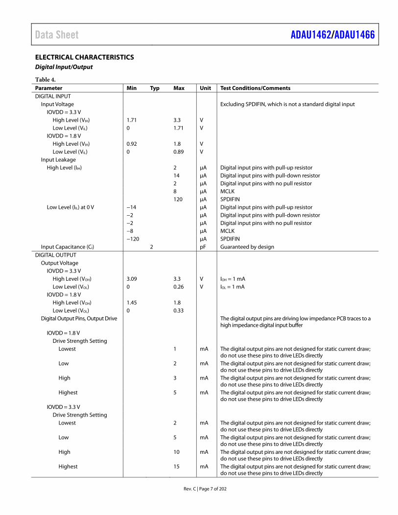
ELECTRICAL CHARACTERISTICS Digital Input/Output
Table 4. Parameter Min Typ Max Unit Test Conditions/Comments DIGITAL INPUT
Input Voltage Excluding SPDIFIN, which is not a standard digital input IOVDD = 3.3 V
High Level (VIH) 1.71 3.3 V Low Level (VIL) 0 1.71 V
IOVDD = 1.8 V High Level (VIH) 0.92 1.8 V Low Level (VIL) 0 0.89 V
Input Leakage High Level (IIH) 2 μA Digital input pins with pull-up resistor
14 μA Digital input pins with pull-down resistor 2 μA Digital input pins with no pull resistor 8 μA MCLK 120 μA SPDIFIN
Low Level (IIL) at 0 V −14 μA Digital input pins with pull-up resistor −2 μA Digital input pins with pull-down resistor −2 μA Digital input pins with no pull resistor −8 μA MCLK −120 μA SPDIFIN Input Capacitance (CI) 2 pF Guaranteed by design
DIGITAL OUTPUT Output Voltage
IOVDD = 3.3 V High Level (VOH) 3.09 3.3 V IOH = 1 mA Low Level (VOL) 0 0.26 V IOL = 1 mA
IOVDD = 1.8 V High Level (VOH) 1.45 1.8 Low Level (VOL) 0 0.33
Digital Output Pins, Output Drive The digital output pins are driving low impedance PCB traces to a high impedance digital input buffer
IOVDD = 1.8 V Drive Strength Setting
Lowest 1 mA The digital output pins are not designed for static current draw; do not use these pins to drive LEDs directly
Low 2 mA The digital output pins are not designed for static current draw; do not use these pins to drive LEDs directly
High 3 mA The digital output pins are not designed for static current draw; do not use these pins to drive LEDs directly
Highest 5 mA The digital output pins are not designed for static current draw; do not use these pins to drive LEDs directly
IOVDD = 3.3 V Drive Strength Setting
Lowest 2 mA The digital output pins are not designed for static current draw; do not use these pins to drive LEDs directly
Low 5 mA The digital output pins are not designed for static current draw; do not use these pins to drive LEDs directly
High 10 mA The digital output pins are not designed for static current draw; do not use these pins to drive LEDs directly
Highest 15 mA The digital output pins are not designed for static current draw; do not use these pins to drive LEDs directly
ADAU1462/ADAU1466 Data Sheet
Rev. C | Page 8 of 202
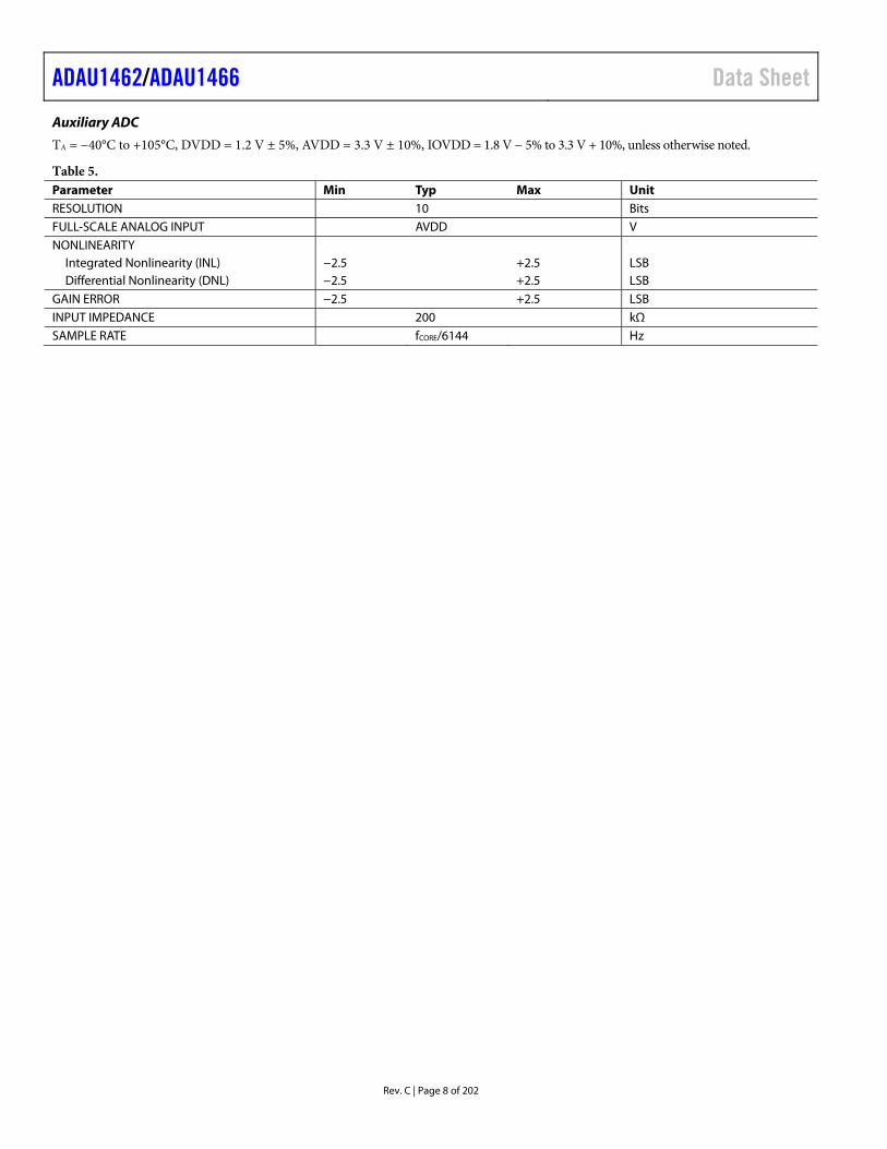
Auxiliary ADC
TA = −40°C to +105°C, DVDD = 1.2 V ± 5%, AVDD = 3.3 V ± 10%, IOVDD = 1.8 V − 5% to 3.3 V + 10%, unless otherwise noted.
Table 5. Parameter Min Typ Max Unit RESOLUTION 10 Bits FULL-SCALE ANALOG INPUT AVDD V NONLINEARITY
Integrated Nonlinearity (INL) −2.5 +2.5 LSB Differential Nonlinearity (DNL) −2.5 +2.5 LSB
GAIN ERROR −2.5 +2.5 LSB INPUT IMPEDANCE 200 kΩ SAMPLE RATE fCORE/6144 Hz
Data Sheet ADAU1462/ADAU1466
Rev. C | Page 9 of 202
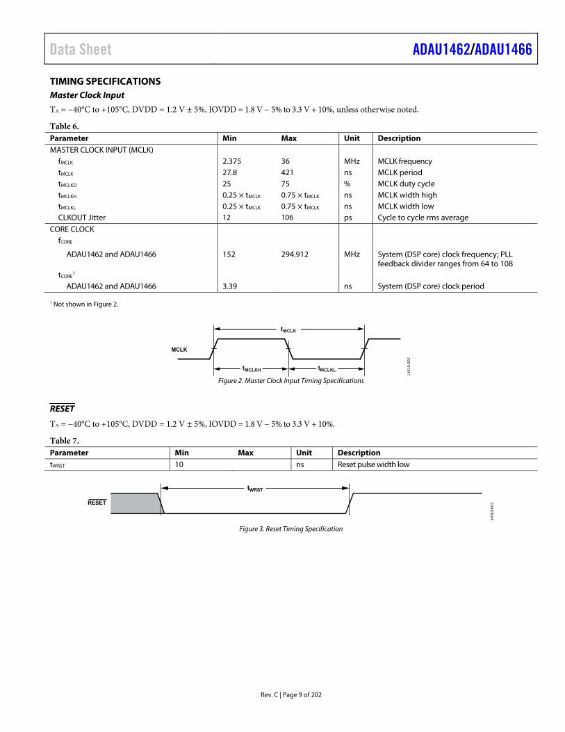
TIMING SPECIFICATIONS Master Clock Input
TA = −40°C to +105°C, DVDD = 1.2 V ± 5%, IOVDD = 1.8 V − 5% to 3.3 V + 10%, unless otherwise noted.
Table 6. Parameter Min Max Unit Description MASTER CLOCK INPUT (MCLK)
fMCLK 2.375 36 MHz MCLK frequency tMCLK 27.8 421 ns MCLK period tMCLKD 25 75 % MCLK duty cycle tMCLKH 0.25 × tMCLK 0.75 × tMCLK ns MCLK width high tMCLKL 0.25 × tMCLK 0.75 × tMCLK ns MCLK width low CLKOUT Jitter 12 106 ps Cycle to cycle rms average
CORE CLOCK fCORE
ADAU1462 and ADAU1466 152 294.912 MHz System (DSP core) clock frequency; PLL feedback divider ranges from 64 to 108
tCORE1
ADAU1462 and ADAU1466 3.39 ns System (DSP core) clock period 1 Not shown in Figure 2.
MCLK
tMCLKH tMCLKL
tMCLK
14
810
-00
2
Figure 2. Master Clock Input Timing Specifications
RESET
TA = −40°C to +105°C, DVDD = 1.2 V ± 5%, IOVDD = 1.8 V − 5% to 3.3 V + 10%.
Table 7. Parameter Min Max Unit Description tWRST 10 ns Reset pulse width low
RESET
tWRST1
48
10
-00
3
Figure 3. Reset Timing Specification
ADAU1462/ADAU1466 Data Sheet
Rev. C | Page 10 of 202
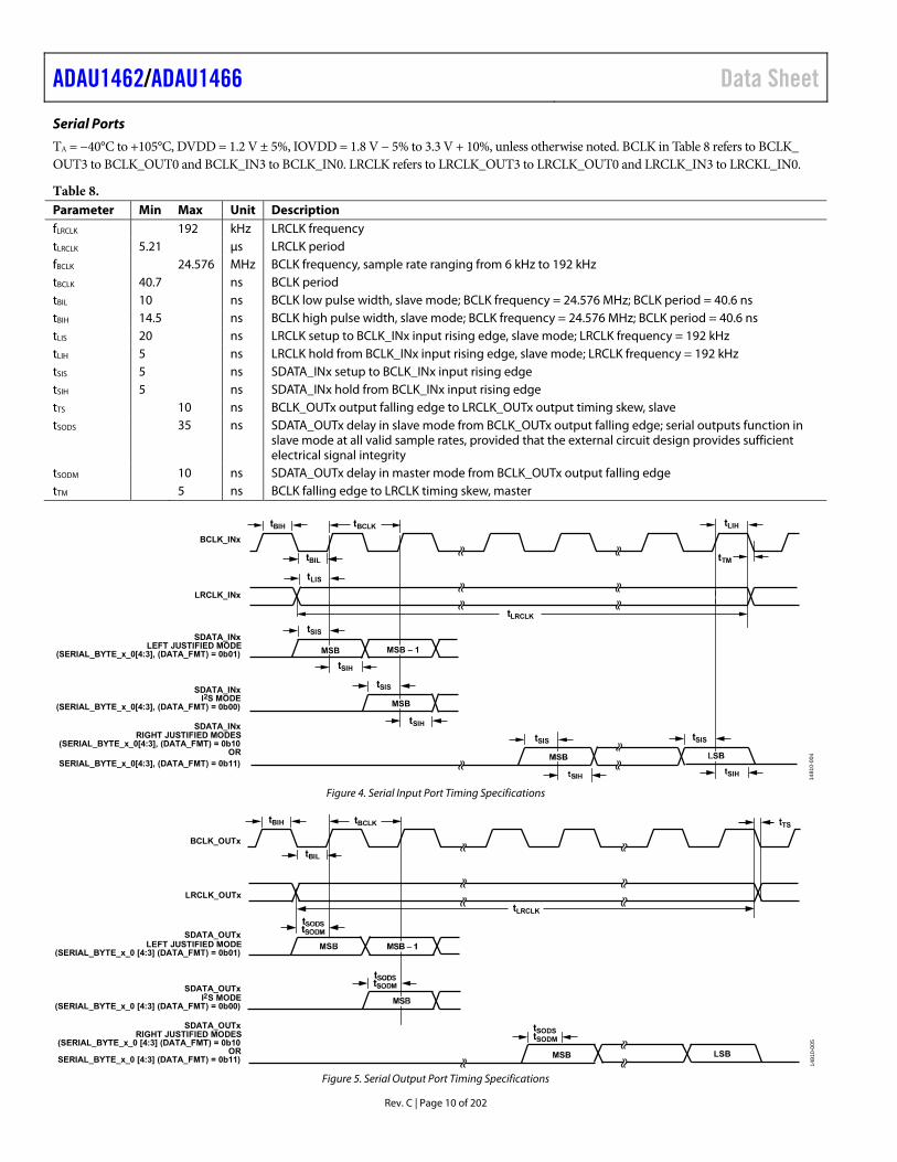
Serial Ports
TA = −40°C to +105°C, DVDD = 1.2 V ± 5%, IOVDD = 1.8 V − 5% to 3.3 V + 10%, unless otherwise noted. BCLK in Table 8 refers to BCLK_ OUT3 to BCLK_OUT0 and BCLK_IN3 to BCLK_IN0. LRCLK refers to LRCLK_OUT3 to LRCLK_OUT0 and LRCLK_IN3 to LRCKL_IN0.
Table 8. Parameter Min Max Unit Description fLRCLK 192 kHz LRCLK frequency tLRCLK 5.21 μs LRCLK period fBCLK 24.576 MHz BCLK frequency, sample rate ranging from 6 kHz to 192 kHz tBCLK 40.7 ns BCLK period tBIL 10 ns BCLK low pulse width, slave mode; BCLK frequency = 24.576 MHz; BCLK period = 40.6 ns tBIH 14.5 ns BCLK high pulse width, slave mode; BCLK frequency = 24.576 MHz; BCLK period = 40.6 ns tLIS 20 ns LRCLK setup to BCLK_INx input rising edge, slave mode; LRCLK frequency = 192 kHz tLIH 5 ns LRCLK hold from BCLK_INx input rising edge, slave mode; LRCLK frequency = 192 kHz tSIS 5 ns SDATA_INx setup to BCLK_INx input rising edge tSIH 5 ns SDATA_INx hold from BCLK_INx input rising edge tTS 10 ns BCLK_OUTx output falling edge to LRCLK_OUTx output timing skew, slave tSODS 35 ns SDATA_OUTx delay in slave mode from BCLK_OUTx output falling edge; serial outputs function in
slave mode at all valid sample rates, provided that the external circuit design provides sufficient electrical signal integrity
tSODM 10 ns SDATA_OUTx delay in master mode from BCLK_OUTx output falling edge tTM 5 ns BCLK falling edge to LRCLK timing skew, master
tBIH tBCLK
tTM
tLIH
MSB MSB – 1
MSB
tLIS
tSIS
tSIH
tSIH
tSIS
tLRCLK
tSIS tSIS
tSIH
tBIL
BCLK_INx
LRCLK_INx
SDATA_INxLEFT JUSTIFIED MODE
(SERIAL_BYTE_x_0[4:3], (DATA_FMT) = 0b01)
SDATA_INxI2S MODE
(SERIAL_BYTE_x_0[4:3], (DATA_FMT) = 0b00)
SDATA_INxRIGHT JUSTIFIED MODES
(SERIAL_BYTE_x_0[4:3], (DATA_FMT) = 0b10OR
SERIAL_BYTE_x_0[4:3], (DATA_FMT) = 0b11)
14
81
0-0
04
Figure 4. Serial Input Port Timing Specifications
BCLK_OUTx
LSB
tBIH
tLRCLK
tBCLK
MSB
TS
tBIL
tSODStSODM
LRCLK_OUTx
SDATA_OUTxLEFT JUSTIFIED MODE
(SERIAL_BYTE_x_0 [4:3] (DATA_FMT) = 0b01)
SDATA_OUTxI2S MODE
(SERIAL_BYTE_x_0 [4:3] (DATA_FMT) = 0b00)
SDATA_OUTxRIGHT JUSTIFIED MODES
(SERIAL_BYTE_x_0 [4:3] (DATA_FMT) = 0b10OR
SERIAL_BYTE_x_0 [4:3] (DATA_FMT) = 0b11)
14
81
0-0
05
Figure 5. Serial Output Port Timing Specifications
Data Sheet ADAU1462/ADAU1466
Rev. C | Page 11 of 202
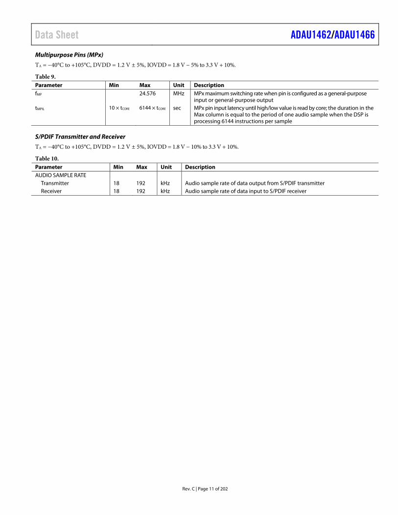
Multipurpose Pins (MPx)
TA = −40°C to +105°C, DVDD = 1.2 V ± 5%, IOVDD = 1.8 V − 5% to 3.3 V + 10%.
Table 9. Parameter Min Max Unit Description fMP 24.576 MHz MPx maximum switching rate when pin is configured as a general-purpose
input or general-purpose output tMPIL 10 × tCORE 6144 × tCORE sec MPx pin input latency until high/low value is read by core; the duration in the
Max column is equal to the period of one audio sample when the DSP is processing 6144 instructions per sample
S/PDIF Transmitter and Receiver
TA = −40°C to +105°C, DVDD = 1.2 V ± 5%, IOVDD = 1.8 V − 10% to 3.3 V + 10%.
Table 10. Parameter Min Max Unit Description AUDIO SAMPLE RATE
Transmitter 18 192 kHz Audio sample rate of data output from S/PDIF transmitter Receiver 18 192 kHz Audio sample rate of data input to S/PDIF receiver
ADAU1462/ADAU1466 Data Sheet
Rev. C | Page 12 of 202
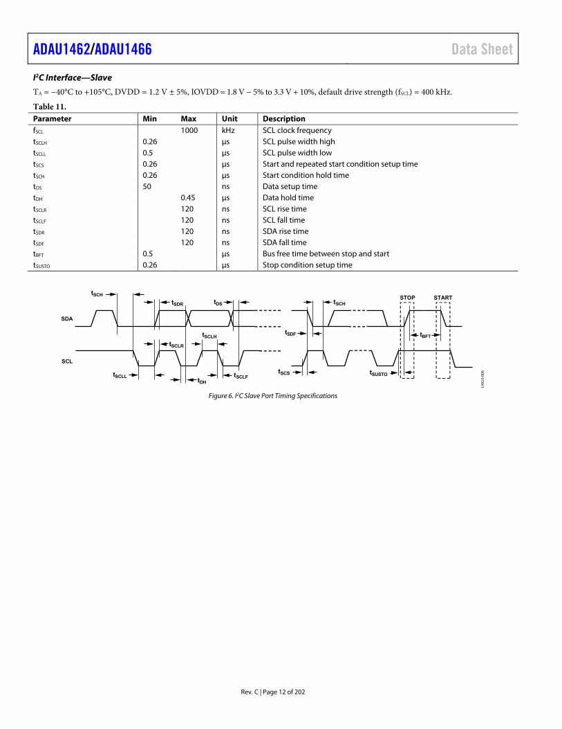
I2C Interface—Slave
TA = −40°C to +105°C, DVDD = 1.2 V ± 5%, IOVDD = 1.8 V − 5% to 3.3 V + 10%, default drive strength (fSCL) = 400 kHz.
Table 11. Parameter Min Max Unit Description fSCL 1000 kHz SCL clock frequency tSCLH 0.26 μs SCL pulse width high tSCLL 0.5 μs SCL pulse width low tSCS 0.26 μs Start and repeated start condition setup time tSCH 0.26 μs Start condition hold time tDS 50 ns Data setup time tDH 0.45 μs Data hold time tSCLR 120 ns SCL rise time tSCLF 120 ns SCL fall time tSDR 120 ns SDA rise time tSDF 120 ns SDA fall time tBFT 0.5 μs Bus free time between stop and start tSUSTO 0.26 μs Stop condition setup time
tSCLH
tSCLR
tSCLL
SDA
SCL
tDH
tSDR
tSCH
tDSSTOP START
tSUSTO
tSCH
tSDF
tSCStSCLF
tBFT
14
810
-00
6
Figure 6. I2C Slave Port Timing Specifications
Data Sheet ADAU1462/ADAU1466
Rev. C | Page 13 of 202
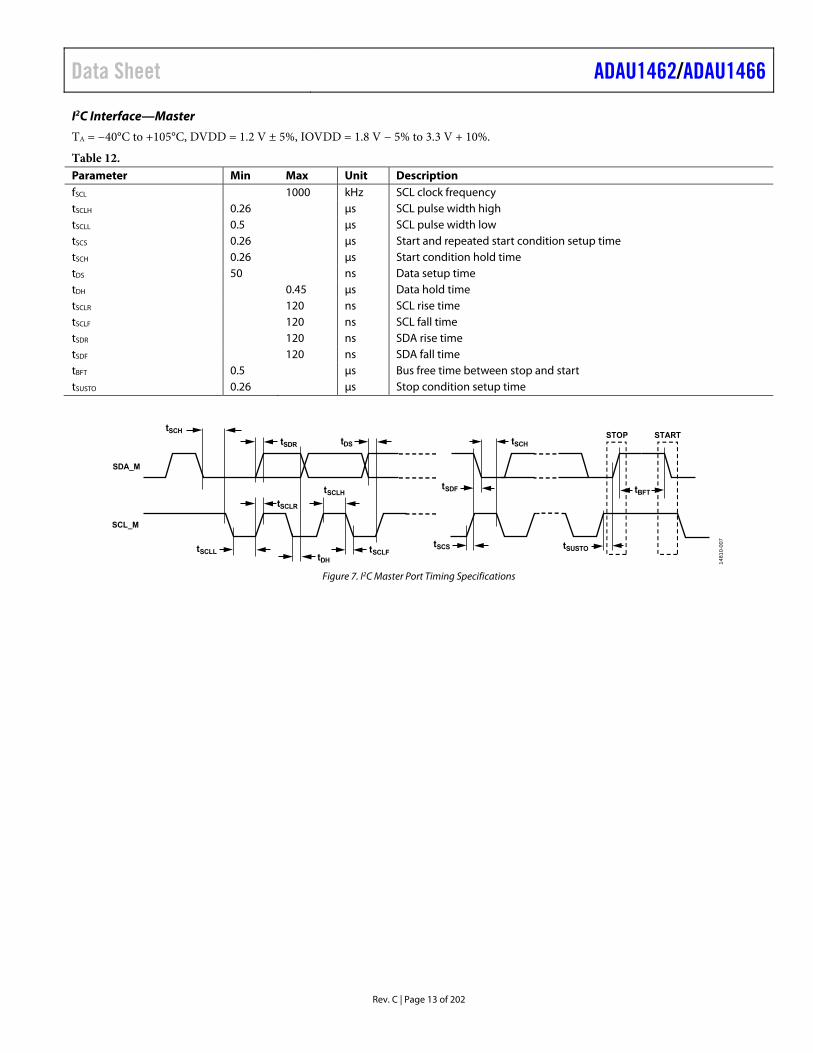
I2C Interface—Master
TA = −40°C to +105°C, DVDD = 1.2 V ± 5%, IOVDD = 1.8 V − 5% to 3.3 V + 10%.
Table 12. Parameter Min Max Unit Description fSCL 1000 kHz SCL clock frequency tSCLH 0.26 μs SCL pulse width high tSCLL 0.5 μs SCL pulse width low tSCS 0.26 μs Start and repeated start condition setup time tSCH 0.26 μs Start condition hold time tDS 50 ns Data setup time tDH 0.45 μs Data hold time tSCLR 120 ns SCL rise time tSCLF 120 ns SCL fall time tSDR 120 ns SDA rise time tSDF 120 ns SDA fall time tBFT 0.5 μs Bus free time between stop and start tSUSTO 0.26 μs Stop condition setup time
SDA_M
SCL_M
tSCLH
tSCLR
tSCLLtDH
tSDR
tSCH
tDSSTOP START
tSUSTO
tSCH
tSDF
tSCStSCLF
tBFT
14
81
0-0
07
Figure 7. I2C Master Port Timing Specifications
ADAU1462/ADAU1466 Data Sheet
Rev. C | Page 14 of 202
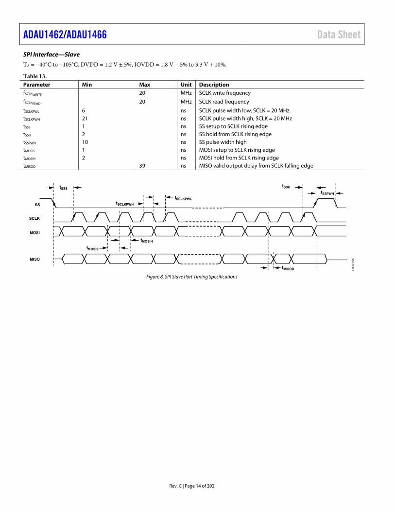
SPI Interface—Slave
TA = −40°C to +105°C, DVDD = 1.2 V ± 5%, IOVDD = 1.8 V − 5% to 3.3 V + 10%.
Table 13. Parameter Min Max Unit Description fSCLKWRITE 20 MHz SCLK write frequency
fSCLKREAD 20 MHz SCLK read frequency
tSCLKPWL 6 ns SCLK pulse width low, SCLK = 20 MHz tSCLKPWH 21 ns SCLK pulse width high, SCLK = 20 MHz tSSS 1 ns SS setup to SCLK rising edge tSSH 2 ns SS hold from SCLK rising edge tSSPWH 10 ns SS pulse width high tMOSIS 1 ns MOSI setup to SCLK rising edge tMOSIH 2 ns MOSI hold from SCLK rising edge tMISOD 39 ns MISO valid output delay from SCLK falling edge
tSSS
tMOSIS
tMOSIH
tMISOD
tSCLKPWH
tSCLKPWL
tSSH
tSSPWH
14
81
0-0
08
Figure 8. SPI Slave Port Timing Specifications
Data Sheet ADAU1462/ADAU1466
Rev. C | Page 15 of 202
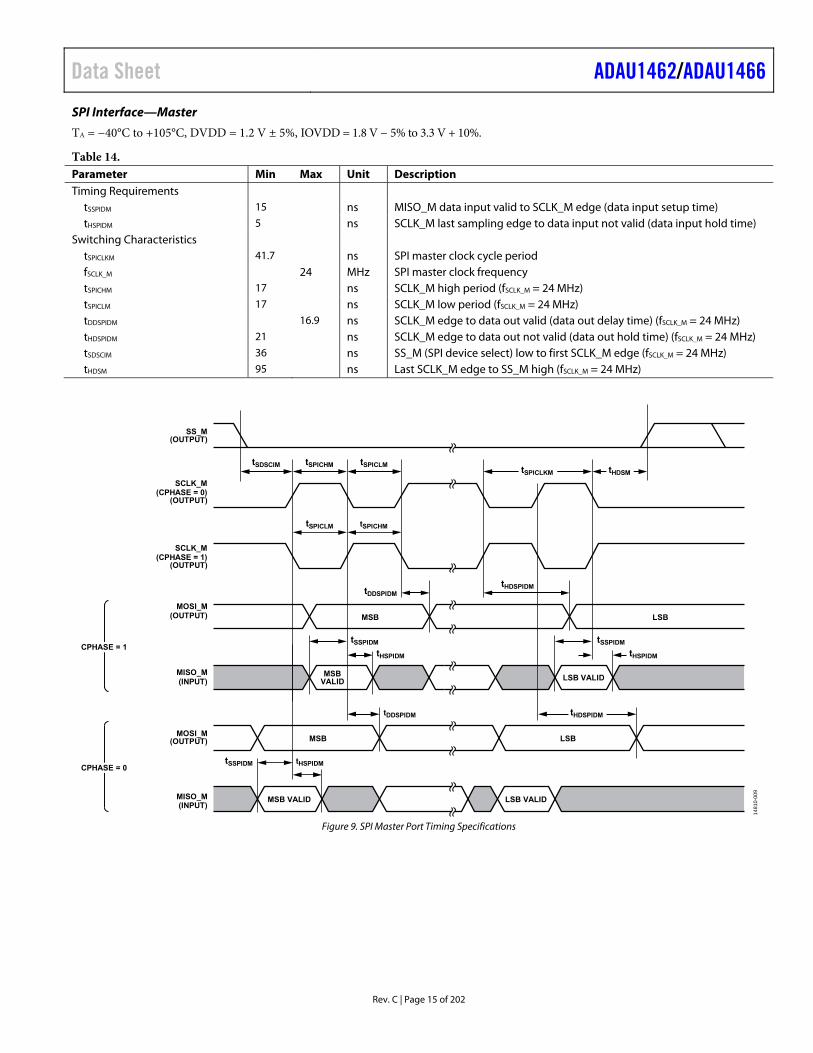
SPI Interface—Master
TA = −40°C to +105°C, DVDD = 1.2 V ± 5%, IOVDD = 1.8 V − 5% to 3.3 V + 10%.
Table 14. Parameter Min Max Unit Description Timing Requirements
tSSPIDM 15 ns MISO_M data input valid to SCLK_M edge (data input setup time) tHSPIDM 5 ns SCLK_M last sampling edge to data input not valid (data input hold time)
Switching Characteristics tSPICLKM 41.7 ns SPI master clock cycle period fSCLK_M 24 MHz SPI master clock frequency tSPICHM 17 ns SCLK_M high period (fSCLK_M = 24 MHz) tSPICLM 17 ns SCLK_M low period (fSCLK_M = 24 MHz) tDDSPIDM 16.9 ns SCLK_M edge to data out valid (data out delay time) (fSCLK_M = 24 MHz) tHDSPIDM 21 ns SCLK_M edge to data out not valid (data out hold time) (fSCLK_M = 24 MHz) tSDSCIM 36 ns SS_M (SPI device select) low to first SCLK_M edge (fSCLK_M = 24 MHz) tHDSM 95 ns Last SCLK_M edge to SS_M high (fSCLK_M = 24 MHz)
tSPICHMtSDSCIM tSPICLMtSPICLKM tHDSM
tSPICLM tSPICHM
MSBVALID
LSB VALIDMSB VALID
LSBMSB
LSBMSB
tDDSPIDM
tHSPIDMtSSPIDM
LSB VALID
CPHASE = 1
CPHASE = 0
tHDSPIDM
tHSPIDM
tSSPIDM
tHSPIDM
tSSPIDM
tDDSPIDM
tHDSPIDM
SS_M(OUTPUT)
SCLK_M(CPHASE = 0)
(OUTPUT)
SCLK_M(CPHASE = 1)
(OUTPUT)
MOSI_M(OUTPUT)
MISO_M(INPUT)
MOSI_M(OUTPUT)
MISO_M(INPUT)
14
81
0-0
09
Figure 9. SPI Master Port Timing Specifications
ADAU1462/ADAU1466 Data Sheet
Rev. C | Page 16 of 202
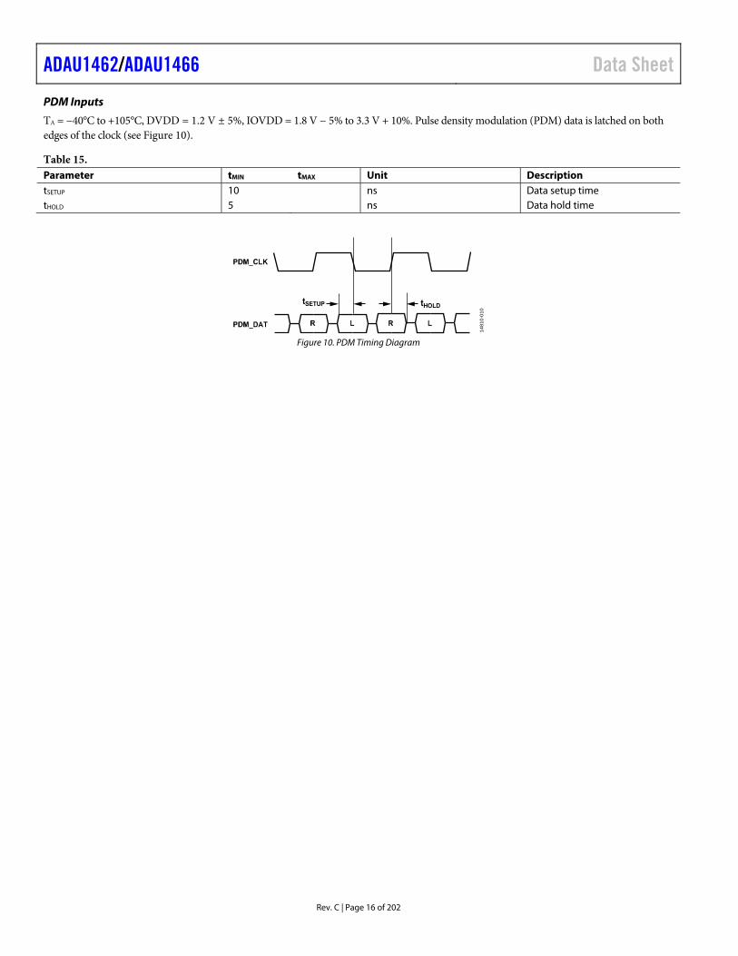
PDM Inputs
TA = −40°C to +105°C, DVDD = 1.2 V ± 5%, IOVDD = 1.8 V − 5% to 3.3 V + 10%. Pulse density modulation (PDM) data is latched on both edges of the clock (see Figure 10).
Table 15. Parameter tMIN tMAX Unit Description tSETUP 10 ns Data setup time tHOLD 5 ns Data hold time
tHOLDtSETUP
14
81
0-0
10
Figure 10. PDM Timing Diagram
Data Sheet ADAU1462/ADAU1466
Rev. C | Page 17 of 202
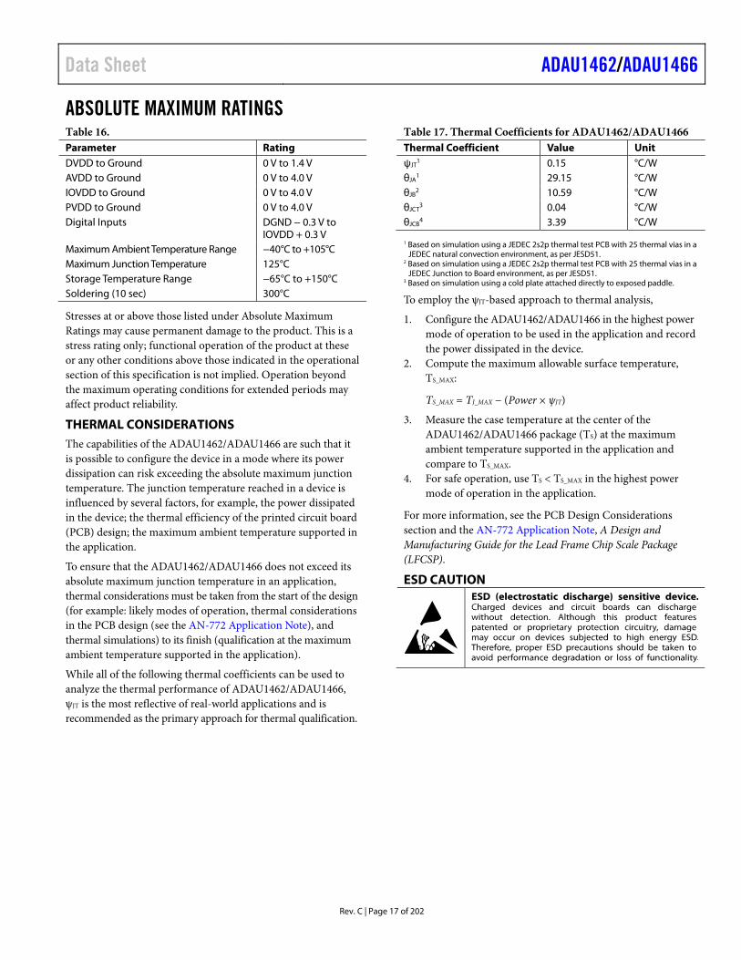
ABSOLUTE MAXIMUM RATINGS Table 16. Parameter Rating DVDD to Ground 0 V to 1.4 V AVDD to Ground 0 V to 4.0 V IOVDD to Ground 0 V to 4.0 V PVDD to Ground 0 V to 4.0 V Digital Inputs DGND − 0.3 V to
IOVDD + 0.3 V Maximum Ambient Temperature Range −40°C to +105°C Maximum Junction Temperature 125°C Storage Temperature Range −65°C to +150°C Soldering (10 sec) 300°C
Stresses at or above those listed under Absolute Maximum Ratings may cause permanent damage to the product. This is a stress rating only; functional operation of the product at these or any other conditions above those indicated in the operational section of this specification is not implied. Operation beyond the maximum operating conditions for extended periods may affect product reliability.
THERMAL CONSIDERATIONS The capabilities of the ADAU1462/ADAU1466 are such that it is possible to configure the device in a mode where its power dissipation can risk exceeding the absolute maximum junction temperature. The junction temperature reached in a device is influenced by several factors, for example, the power dissipated in the device; the thermal efficiency of the printed circuit board (PCB) design; the maximum ambient temperature supported in the application.
To ensure that the ADAU1462/ADAU1466 does not exceed its absolute maximum junction temperature in an application, thermal considerations must be taken from the start of the design (for example: likely modes of operation, thermal considerations in the PCB design (see the AN-772 Application Note), and thermal simulations) to its finish (qualification at the maximum ambient temperature supported in the application).
While all of the following thermal coefficients can be used to analyze the thermal performance of ADAU1462/ADAU1466, ψJT is the most reflective of real-world applications and is recommended as the primary approach for thermal qualification.
Table 17. Thermal Coefficients for ADAU1462/ADAU1466 Thermal Coefficient Value Unit ψJT
1 0.15 °C/W θJA
1 29.15 °C/W θJB
2 10.59 °C/W θJCT
3 0.04 °C/W θJCB
4 3.39 °C/W 1 Based on simulation using a JEDEC 2s2p thermal test PCB with 25 thermal vias in a
JEDEC natural convection environment, as per JESD51. 2 Based on simulation using a JEDEC 2s2p thermal test PCB with 25 thermal vias in a
JEDEC Junction to Board environment, as per JESD51. 3 Based on simulation using a cold plate attached directly to exposed paddle.
To employ the ψJT-based approach to thermal analysis,
1. Configure the ADAU1462/ADAU1466 in the highest power mode of operation to be used in the application and record the power dissipated in the device.
2. Compute the maximum allowable surface temperature, TS_MAX:
TS_MAX = TJ_MAX − (Power × ψJT)
3. Measure the case temperature at the center of the ADAU1462/ADAU1466 package (TS) at the maximum ambient temperature supported in the application and compare to TS_MAX.
4. For safe operation, use TS < TS_MAX in the highest power mode of operation in the application.
For more information, see the PCB Design Considerations section and the AN-772 Application Note, A Design and Manufacturing Guide for the Lead Frame Chip Scale Package (LFCSP).
ESD CAUTION
ADAU1462/ADAU1466 Data Sheet
Rev. C | Page 18 of 202
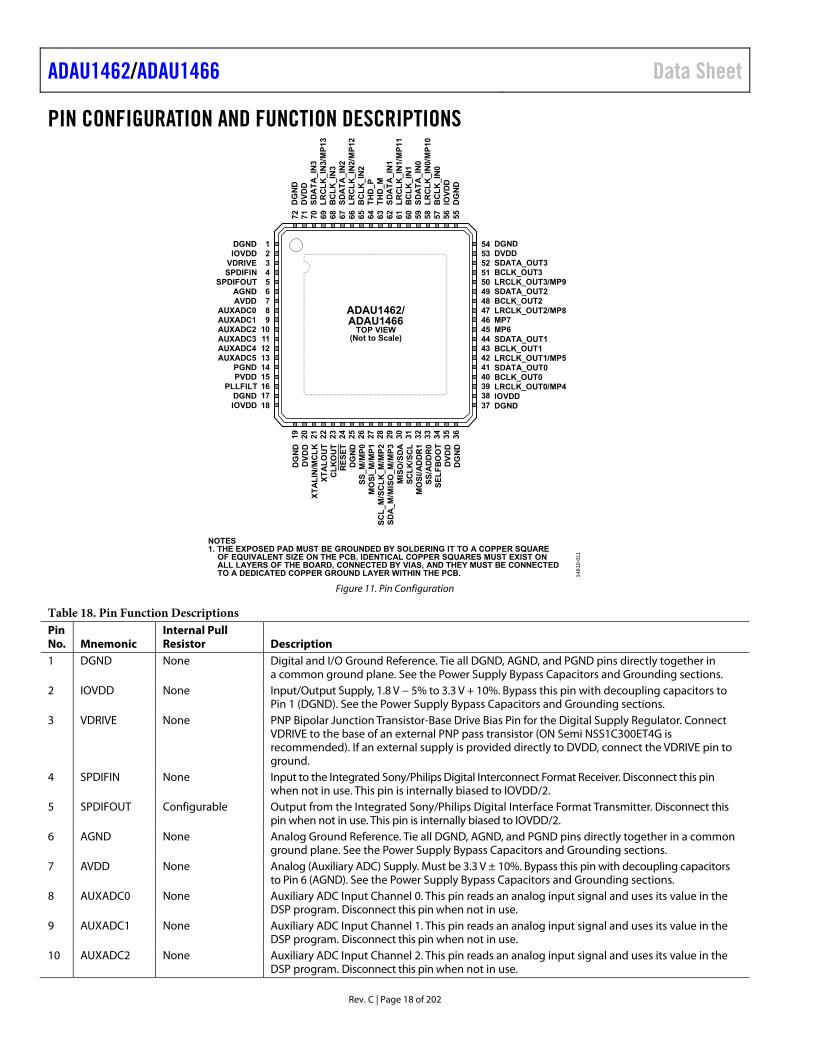
PIN CONFIGURATION AND FUNCTION DESCRIPTIONS
DG
ND
DGND
DG
ND
DGNDDVDDSDATA_OUT3BCLK_OUT3LRCLK_OUT3/MP9SDATA_OUT2BCLK_OUT2LRCLK_OUT2/MP8MP7MP6SDATA_OUT1BCLK_OUT1LRCLK_OUT1/MP5SDATA_OUT0BCLK_OUT0LRCLK_OUT0/MP4IOVDDDGND
123456789
101112131415161718
19 20 21 22 23 24 25 26 27 28 29 30 31 32 33 34 35 36
545352515049484746454443424140393837
72 71 70 69 68 67 66 65 64 63 62 61 60 59 58 57 56 55
ADAU1462/ADAU1466
TOP VIEW(Not to Scale)
DV
DD
SD
AT
A_I
N3
LR
CL
K_I
N3/
MP
13B
CL
K_I
N3
SD
AT
A_I
N2
LR
CL
K_I
N2/
MP
12B
CL
K_I
N2
TH
D_P
TH
D_M
SD
AT
A_I
N1
LR
CL
K_I
N1/
MP
11B
CL
K_I
N1
SD
AT
A_I
N0
LR
CL
K_I
N0/
MP
10B
CL
K_I
N0
IOV
DD
DG
ND
IOVDDVDRIVESPDIFIN
SPDIFOUTAGNDAVDD
AUXADC0AUXADC1AUXADC2AUXADC3AUXADC4AUXADC5
PGNDPVDD
PLLFILTDGNDIOVDD
DV
DD
XT
AL
IN/M
CL
KX
TA
LO
UT
CL
KO
UT
RE
SE
TD
GN
DS
S_M
/MP
0M
OS
I_M
/MP
1S
CL
_M/S
CL
K_M
/MP
2S
DA
_M/M
ISO
_M/M
P3
MIS
O/S
DA
SC
LK
/SC
LM
OS
I/A
DD
R1
SS
/AD
DR
0S
EL
FB
OO
TD
VD
DD
GN
D
NOTES1. THE EXPOSED PAD MUST BE GROUNDED BY SOLDERING IT TO A COPPER SQUARE OF EQUIVALENT SIZE ON THE PCB. IDENTICAL COPPER SQUARES MUST EXIST ON ALL LAYERS OF THE BOARD, CONNECTED BY VIAS, AND THEY MUST BE CONNECTED TO A DEDICATED COPPER GROUND LAYER WITHIN THE PCB. 1
48
10
-011
Figure 11. Pin Configuration
Table 18. Pin Function Descriptions Pin No. Mnemonic
Internal Pull Resistor Description
1 DGND None Digital and I/O Ground Reference. Tie all DGND, AGND, and PGND pins directly together in a common ground plane. See the Power Supply Bypass Capacitors and Grounding sections.
2 IOVDD None Input/Output Supply, 1.8 V − 5% to 3.3 V + 10%. Bypass this pin with decoupling capacitors to Pin 1 (DGND). See the Power Supply Bypass Capacitors and Grounding sections.
3 VDRIVE None PNP Bipolar Junction Transistor-Base Drive Bias Pin for the Digital Supply Regulator. Connect VDRIVE to the base of an external PNP pass transistor (ON Semi NSS1C300ET4G is recommended). If an external supply is provided directly to DVDD, connect the VDRIVE pin to ground.
4 SPDIFIN None Input to the Integrated Sony/Philips Digital Interconnect Format Receiver. Disconnect this pin when not in use. This pin is internally biased to IOVDD/2.
5 SPDIFOUT Configurable Output from the Integrated Sony/Philips Digital Interface Format Transmitter. Disconnect this pin when not in use. This pin is internally biased to IOVDD/2.
6 AGND None Analog Ground Reference. Tie all DGND, AGND, and PGND pins directly together in a common ground plane. See the Power Supply Bypass Capacitors and Grounding sections.
7 AVDD None Analog (Auxiliary ADC) Supply. Must be 3.3 V ± 10%. Bypass this pin with decoupling capacitors to Pin 6 (AGND). See the Power Supply Bypass Capacitors and Grounding sections.
8 AUXADC0 None Auxiliary ADC Input Channel 0. This pin reads an analog input signal and uses its value in the DSP program. Disconnect this pin when not in use.
9 AUXADC1 None Auxiliary ADC Input Channel 1. This pin reads an analog input signal and uses its value in the DSP program. Disconnect this pin when not in use.
10 AUXADC2 None Auxiliary ADC Input Channel 2. This pin reads an analog input signal and uses its value in the DSP program. Disconnect this pin when not in use.
Data Sheet ADAU1462/ADAU1466
Rev. C | Page 19 of 202
Pin No. Mnemonic
Internal Pull Resistor Description
11 AUXADC3 None Auxiliary ADC Input Channel 3. This pin reads an analog input signal and uses its value in the DSP program. Disconnect this pin when not in use.
12 AUXADC4 None Auxiliary ADC Input Channel 4. This pin reads an analog input signal and uses its value in the DSP program. Disconnect this pin when not in use.
13 AUXADC5 None Auxiliary ADC Input Channel 5. This pin reads an analog input signal and uses its value in the DSP program. Disconnect this pin when not in use.
14 PGND None PLL Ground Reference. Tie all DGND, AGND, and PGND pins directly together in a common ground plane. See the Power Supply Bypass Capacitors and Grounding sections.
15 PVDD None PLL Supply. Must be 3.3 V ± 10%. Bypass this pin with decoupling capacitors to Pin 14 (PGND). See the Power Supply Bypass Capacitors and Grounding sections.
16 PLLFILT None PLL Filter. The voltage on the PLLFILT pin, which is internally generated, is typically between 1.65 V and 2.10 V.
17 DGND None Digital and I/O Ground Reference. Tie all DGND, AGND, and PGND pins directly together in a common ground plane. See the Power Supply Bypass Capacitors and Grounding sections.
18 IOVDD None Input/Output Supply, 1.8 V − 5% to 3.3 V + 10%. Bypass this pin to Pin 17 (DGND) with decoupling capacitors. See the Power Supply Bypass Capacitors and Grounding sections.
19 DGND None Digital and I/O Ground Reference. Tie all DGND, AGND, and PGND pins directly together in a common ground plane. See the Power Supply Bypass Capacitors and Grounding sections.
20 DVDD None Digital Supply. Must be 1.2 V ± 5%. This pin can be supplied externally or by using the internal regulator and external pass transistor. Bypass this pin to Pin 19 (DGND) with decoupling capacitors. See the Power Supply Bypass Capacitors and Grounding sections.
21 XTALIN/MCLK None Crystal Oscillator Input (XTALIN)/Master Clock Input to the PLL (MCLK). This pin can be supplied directly or generated by driving a crystal with the internal crystal oscillator via Pin 22 (XTALOUT). If a crystal is used, refer to the circuit shown in Figure 14.
22 XTALOUT None Crystal Oscillator Output for Driving an External Crystal. If a crystal is used, refer to the circuit shown in Figure 14. Disconnect this pin when not in use.
23 CLKOUT Configurable Master Clock Output. This pin drives a master clock signal to other ICs in the system. CLKOUT can be configured to output a clock signal with a frequency of 1×, 2×, 4×, or 8× the frequency of the divided clock signal being input to the PLL. Disconnect this pin when not in use.
24 RESET Pull-down Active Low Reset Input. A reset is triggered on a high to low edge and exited on a low to high edge. A reset event sets all RAMs and registers to their default values.
25 DGND None Digital and I/O Ground Reference. Tie all DGND, AGND, and PGND pins directly together in a common ground plane. See the Power Supply Bypass Capacitors and Grounding sections.
26 SS_M/MP0 Pull-up; nominally 250 kΩ; can be disabled by a write to control register
SPI Master/Slave Select Port (SS_M)/Multipurpose, General-Purpose Input/Output (MP0). When in SPI master mode, this pin acts as the slave select signal to slave devices on the SPI bus. The pin must go low at the beginning of a master SPI transaction and high at the end of a transaction. This pin has an internal pull-up resistor that is nominally 250 kΩ. When the SELFBOOT pin is held high and the RESET pin has a transition from low to high, Pin 26 sets the communications protocol for self boot operation. If this pin is left floating, the SPI communications protocol is used for self boot operation. If this pin has a 10 kΩ pull-down resistor to DGND, the I2C communications protocol is used for self boot operation. When self boot operation is not used and this pin is not needed as a general-purpose input or output, leave it disconnected.
27 MOSI_M/MP1 Pull-up; can be disabled by a write to control register
SPI Master Data Output Port (MOSI_M)/Multipurpose, General-Purpose Input/Output (MP1). When in SPI master mode, this pin sends data from the SPI master port to slave devices on the SPI bus. Disconnect this pin when not in use.
28 SCL_M/ SCLK_M/MP2
Pull-up; can be disabled by a write to control register
I2C Master Serial Clock Port (SCL_M)/SPI Master Mode Serial Clock (SCLK_M)/Multipurpose, General-Purpose Input/Output (MP2). When in I2C master mode, this pin functions as an open collector output and drives a serial clock to slave devices on the I2C bus; use a 2.0 kΩ pull-up resistor to IOVDD on the line connected to this pin. When in SPI master mode, this pin drives the clock signal to slave devices on the SPI bus. Disconnect this pin when not in use.
29 SDA_M/ MISO_M/MP3
Pull-up; can be disabled by a write to control register
I2C Master Port Serial Data (SDA_M)/SPI Master Mode Data Input (MISO_M)/Multipurpose, General-Purpose Input/Output (MP3). When in I2C master mode, this pin functions as a bi-directional open collector data line between the I2C master port and slave devices on the I2C bus; use a 2.0 kΩ pull-up resistor to IOVDD on the line connected to this pin. When in SPI master mode, this pin receives data from slave devices on the SPI bus. Disconnect this pin when not in use.
ADAU1462/ADAU1466 Data Sheet
Rev. C | Page 20 of 202
Pin No. Mnemonic
Internal Pull Resistor Description
30 MISO/SDA Pull-up; can be disabled by a write to control register
SPI Slave Data Output Port (MISO)/I2C Slave Serial Data Port (SDA). In SPI slave mode, this pin outputs data to the master device on the SPI bus. In I2C slave mode, this pin functions as a bi-directional open collector data line between the I2C slave port and the master device on the I2C bus; use a 2.0 kΩ pull-up resistor to IOVDD on the line connected to this pin. When this pin is not in use, connect it to IOVDD with a 10.0 kΩ pull-up resistor.
31 SCLK/SCL Pull-up; can be disabled by a write to control register
SPI Slave Port Serial Clock (SCLK)/I2C Slave Port Serial Clock (SCL). In SPI slave mode, this pin receives the serial clock signal from the master device on the SPI bus. In I2C slave mode, this pin receives the serial clock signal from the master device on the I2C bus; use a 2.0 kΩ pull-up resistor to IOVDD on the line connected to this pin. When this pin is not in use, connect it to IOVDD with a 10.0 kΩ pull-up resistor.
32 MOSI/ADDR1 Pull-up; can be disabled by a write to control register
SPI Slave Port Data Input (MOSI)/I2C Slave Port Address MSB (ADDR1). In SPI slave mode, this pin receives a data signal from the master device on the SPI bus. In I2C slave mode, this pin acts as an input and sets the chip address of the I2C slave port, in conjunction with Pin 33 (SS/ADDR0).
33 SS/ADDR0 Pull-up, nominally 250 kΩ; can be disabled by a write to control register
SPI Slave Port Slave Select (SS)/I2C Slave Port Address LSB (ADDR0). In SPI slave mode, this pin receives the slave select signal from the master device on the SPI bus. In I2C slave mode, this pin acts as an input and sets the chip address of the I2C slave port in conjunction with Pin 32 (MOSI/ADDR1).
34 SELFBOOT Pull-up Self Boot Select. This pin allows the device to perform a self boot, in which it loads its random access memory (RAM) and register settings from an external EEPROM. Connecting Pin 34 to logic high (IOVDD) initiates a self boot operation the next time there is a rising edge on Pin 24 (RESET). When this pin is connected to ground, no self boot operation is initiated. This pin can be connected to IOVDD or to ground either directly or pulled up or down with a 1.0 kΩ or larger resistor.
35 DVDD None Digital Supply. Must be 1.2 V ± 5%. This pin can be supplied externally or by using the internal regulator and external pass transistor. Bypass this pin to Pin 36 (DGND) with decoupling capacitors. See the Power Supply Bypass Capacitors and Grounding sections.
36 DGND None Digital and I/O Ground Reference. Tie all DGND, AGND, and PGND pins directly together in a common ground plane. See the Power Supply Bypass Capacitors and Grounding sections.
37 DGND None Digital and I/O Ground Reference. Tie all DGND, AGND, and PGND pins directly together in a common ground plane. See the Power Supply Bypass Capacitors and Grounding sections.
38 IOVDD None Input/Output Supply, 1.8 V − 5% to 3.3 V + 10%. Bypass this pin with decoupling capacitors to Pin 37 (DGND). See the Power Supply Bypass Capacitors and Grounding sections.
39 LRCLK_OUT0/ MP4
Configurable Frame Clock, Serial Output Port 0 (LRCLK_OUT0)/Multipurpose, General-Purpose Input/Output (MP4). This pin is bidirectional, with the direction depending on whether Serial Output Port 0 is a master or slave. Disconnect this pin when not in use.
40 BCLK_OUT0 Configurable Bit Clock, Serial Output Port 0. This pin is bidirectional, with the direction depending on whether the Serial Output Port 0 is a master or slave. Disconnect this pin when not in use.
41 SDATA_OUT0 Configurable Serial Data Output Port 0 (Channel 0 to Channel 15). Capable of 2-channel, 4-channel, 8-channel, and 16-channel modes. Disconnect this pin when not in use.
42 LRCLK_OUT1/ MP5
Configurable Frame Clock, Serial Output Port 1 (LRCLK_OUT1)/Multipurpose, General-Purpose Input/Output (MP5). This pin is bidirectional, with the direction depending on whether Serial Output Port 1 is a master or slave. Disconnect this pin when not in use.
43 BCLK_OUT1 Configurable Bit Clock, Serial Output Port 1. This pin is bidirectional, with the direction depending on whether Output Serial Port 1 is a master or slave. Disconnect this pin when not in use.
44 SDATA_OUT1 Configurable Serial Data Output Port 1 (Channel 16 to Channel 31). Capable of 2-channel, 4-channel, 8-channel, and 16-channel modes. Disconnect this pin when not in use.
45 MP6 Configurable Multipurpose, General-Purpose Input/Output 6. Disconnect this pin when not in use. 46 MP7 Configurable Multipurpose, General-Purpose Input/Output 7. Disconnect this pin when not in use. 47 LRCLK_OUT2/
MP8 Configurable Frame Clock, Serial Output Port 2 (LRCLK_OUT2)/Multipurpose, General-Purpose Input/Output
(MP8). This pin is bidirectional, with the direction depending on whether Serial Output Port 2 is a master or slave. Disconnect this pin when not in use.
48 BCLK_OUT2 Configurable Bit Clock, Serial Output Port 2. This pin is bidirectional, with the direction depending on whether Serial Output Port 2 is a master or slave. Disconnect this pin when not in use.
49 SDATA_OUT2 Configurable Serial Data Output Port 2 (Channel 32 to Channel 39). Capable of 2-channel, 4-channel, 8-channel, or flexible TDM mode. Disconnect this pin when not in use.
50 LRCLK_OUT3/ MP9
Configurable Frame Clock, Serial Output Port 3 (LRCLK_OUT3)/Multipurpose, General-Purpose Input/Output (MP9). This pin is bidirectional, with the direction depending on whether Serial Output Port 3 is a master or slave. Disconnect this pin when not in use.
Data Sheet ADAU1462/ADAU1466
Rev. C | Page 21 of 202
Pin No. Mnemonic
Internal Pull Resistor Description
51 BCLK_OUT3 Configurable Bit Clock, Serial Output Port 3. This pin is bidirectional, with the direction depending on whether Serial Output Port 3 is a master or slave. Disconnect this pin when not in use.
52 SDATA_OUT3 Configurable Serial Data Output Port 3 (Channel 40 to Channel 47). Capable of 2-channel, 4-channel, 8-channel, and flexible TDM modes. Disconnect this pin when not in use.
53 DVDD None Digital Supply. Must be 1.2 V ± 5%. This pin can be supplied externally or by using the internal regulator and external pass transistor. Bypass Pin 53 with decoupling capacitors to Pin 54 (DGND). See the Power Supply Bypass Capacitors and Grounding sections.
54 DGND None Digital and I/O Ground Reference. Tie all DGND, AGND, and PGND pins directly together in a common ground plane. See the Power Supply Bypass Capacitors and Grounding sections.
55 DGND None Digital and I/O Ground Reference. Tie all DGND, AGND, and PGND pins directly together in a common ground plane. See the Power Supply Bypass Capacitors and Grounding sections.
56 IOVDD None Input/Output Supply, 1.8 V − 5% to 3.3 V + 10%. Bypass this pin with decoupling capacitors to Pin 55 (DGND). See the Power Supply Bypass Capacitors and Grounding sections.
57 BCLK_IN0 Configurable Bit Clock, Serial Input Port 0. This pin is bidirectional, with the direction depending on whether Serial Input Port 0 is a master or slave. Disconnect this pin when not in use.
58 LRCLK_IN0/ MP10
Configurable Frame Clock, Serial Input Port 0 (LRCLK_IN0)/Multipurpose, General-Purpose Input/Output (MP10). This pin is bidirectional, with the direction depending on whether Serial Input Port 0 is a master or slave. Disconnect this pin when not in use.
59 SDATA_IN0 Configurable Serial Data Input Port 0 (Channel 0 to Channel 15). Capable of 2-channel, 4-channel, 8-channel, or 16-channel mode. Disconnect this pin when not in use.
60 BCLK_IN1 Configurable Bit Clock, Serial Input Port 1. This pin is bidirectional, with the direction depending on whether the Serial Input Port 1 is a master or slave. Disconnect this pin when not in use.
61 LRCLK_IN1/ MP11
Configurable Frame Clock, Serial Input Port 1 (LRCLK_IN1)/Multipurpose, General-Purpose Input/Output (MP11). This pin is bidirectional, with the direction depending on whether the Serial Input Port 1 is a master or slave. Disconnect this pin when not in use.
62 SDATA_IN1 Configurable Serial Data Input Port 1 (Channels 16 to Channel 31). Capable of 2-channel, 4-channel, 8-channel, or 16-channel mode. Disconnect this pin when not in use.
63 THD_M None Thermal Diode Negative (−) Input. Connect this pin to the D− pin of an external temperature sensor IC. Disconnect this pin when not in use.
64 THD_P None Thermal Diode Positive (+) Input. Connect this pin to the D+ pin of an external temperature sensor IC. Disconnect this pin when not in use.
65 BCLK_IN2 Configurable Bit Clock, Serial Input Port 2. This pin is bidirectional, with the direction depending on whether the Serial Input Port 2 is a master or slave. Disconnect this pin when not in use.
66 LRCLK_IN2/ MP12
Configurable Frame Clock, Input Serial Port 2 (LRCLK_IN2)/Multipurpose, General-Purpose Input/Output (MP12). This pin is bidirectional, with the direction depending on whether Serial Input Port 2 is a master or slave. Disconnect this pin when not in use.
67 SDATA_IN2 Configurable Serial Data Input Port 2 (Channel 32 to Channel 39). Capable of 2-channel, 4-channel, 8-channel, or flexible TDM mode. Disconnect this pin when not in use.
68 BCLK_IN3 Configurable Bit Clock, Input Serial Port 3. This pin is bidirectional, with the direction depending on whether Input Serial Port 3 is a master or slave. Disconnect this pin when not in use.
69 LRCLK_IN3/ MP13
Configurable Frame Clock, Serial Input Port 3 (LRCLK_IN3)/Multipurpose, General-Purpose Input/Output (MP13). This pin is bidirectional, with the direction depending on whether Serial Input Port 3 is a master or slave. Disconnect this pin when not in use.
70 SDATA_IN3 Configurable Serial Data Input Port 3 (Channel 40 to Channel 47). Capable of 2-channel, 4-channel, 8-channel, or flexible TDM mode. Disconnect this pin when not in use.
71 DVDD None Digital Supply. Must be 1.2 V ± 5%. This pin can be supplied externally or by using the internal regulator and external pass transistor. Bypass with decoupling capacitors to Pin 72 (DGND).
72 DGND None Digital and I/O Ground Reference. Tie all DGND, AGND, and PGND pins directly together in a common ground plane. See the Power Supply Bypass Capacitors and Grounding sections.
EP Exposed Pad None The exposed pad must be grounded by soldering it to a copper square of equivalent size on the PCB. Identical copper squares must exist on all layers of the board, connected by vias, and they must be connected to a dedicated copper ground layer within the PCB. See Exposed Pad PCB Design, Figure 87, and Figure 88.
ADAU1462/ADAU1466 Data Sheet
Rev. C | Page 22 of 202
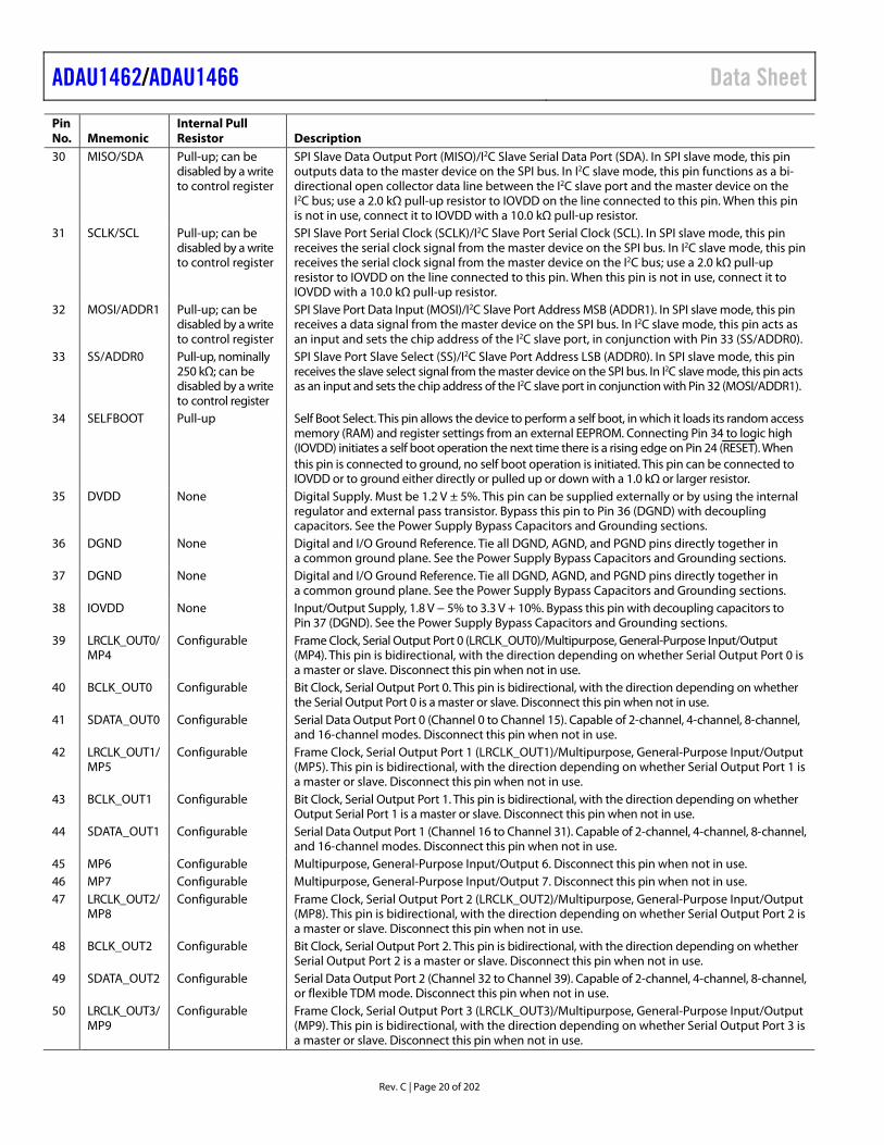
THEORY OF OPERATION SYSTEM BLOCK DIAGRAM
PLLLOOP
FILTER
CRYSTALRESONATOR
CONTROL CIRCUITRY
(PUSH BUTTONS,ROTARY
ENCODERS,POTENTIOMETERS)
SELF BOOTMEMORY
SYSTEM HOSTCONTROLLER
(MICROCONTROLLER,MICROPROCESSOR)
S/PDIF OPTICALRECEIVER
AUDIOADCS
MEMSMICROPHONES
AUDIO SOURCES
POWERSUPPLY
TEMPERATURESENSOR
CONTROLLER
DIGITALAUDIO
SOURCES
S/PDIF OPTICALTRANSMITTER
AUDIODACS
AUDIO SINKS
DIGITALAUDIOSINKS
LPF
S/PDIFTRANSMITTER1
S/PDIFRECEIVER1
8× 2-CHANNELASYNCHRONOUS
SAMPLE RATECONVERTERSINPUT
CLOCKDOMAINS
(×4)
OUTPUTCLOCK
DOMAINS(×4)
CLOCKOSCILLATOR
GPIO/AUX ADC PLL
I2C/SPISLAVE
REGULATOR
ADAU1462/ADAU1466
TEMPERATURESENSOR
I2C/SPIMASTER
DIGITALMIC INPUT
SERIAL DATAINPUT PORTS
(×4)SERIAL DATA
OUTPUT PORTS(×4)
DEJITTER ANDCLOCK GENERATOR
INPUT AUDIOROUTING MATRIX
OUTPUT AUDIOROUTING MATRIX
294.912MHzPROGRAMMABLE AUDIO
PROCESSING CORE
RAM, ROM, WATCHDOG,MEMORY PARITY CHECK
14
81
0-0
12
Figure 12. System Block Diagram with Example Connections to External Components
OVERVIEW The ADAU1462/ADAU1466 are enhanced audio processors with 48 channels of input and output. They include options for the hardware routing of audio signals between the various inputs, outputs, SigmaDSP core, and integrated sample rate converters. The SigmaDSP core features full 32-bit processing (that is, 64-bit processing in double precision mode) with an 80-bit arithmetic logic unit (ALU). By using a quadruple multiply accumulator (MAC) data path, the ADAU1462/ADAU1466 can execute more than 1.2 billion MAC operations per second, which allows processing power that far exceeds predecessors in the SigmaDSP family of products. The powerful DSP core can process over 3,000 double precision biquad filters or 24,000 FIR filter taps per sample at the standard 48 kHz audio sampling rate. Other features, including synchronous parameter loading for ensuring filter stability and 100% code efficiency with the SigmaStudio tools, reduce complexity in audio system development. The SigmaStudio library of audio processing algorithms allows system designers to compensate for real-world limitations of speakers, amplifiers, and listening environments, through speaker equalization, multiband compression, limiting, and third party branded algorithms.
The input audio routing matrix and output audio routing matrix allow the user to multiplex inputs from multiple sources that are running at various sample rates to or from the SigmaDSP core, and then to pass them on to the desired hardware outputs. This multiplexing drastically reduces the complexity of signal routing and clocking issues in the audio system. The audio subsystem includes eight stereo ASRCs, S/PDIF input and output, and serial audio data ports supporting 2 to 16 channels in formats such as I2S and time division multiplexing (TDM). Any of the inputs can be routed to the SigmaDSP core or to any of the ASRCs. Similarly, the output signals can be taken from the SigmaDSP core, any of the ASRC outputs, the serial inputs, the PDM microphones, or the S/PDIF receiver. This routing scheme, which can be modified at any time using control registers, allows maximum system flexibility without requiring hardware design changes.
Two serial input ports and two serial output ports can operate as pairs in a special flexible TDM mode, allowing the user to assign byte specific locations independently to audio streams at varying bit depths. This mode ensures compatibility with codecs that use similar flexible TDM streams.
Data Sheet ADAU1462/ADAU1466
Rev. C | Page 23 of 202
The DSP core is optimized for audio processing, and it can process audio at sample rates of up to 192 kHz. The program and parameter/data RAMs can be loaded with a custom audio processing signal flow built with the SigmaStudio graphical programming software from Analog Devices, Inc., which is available for download at www.analog.com. The values that are stored in the parameter RAM can control individual signal processing blocks, such as infinite impulse response (IIR) and finite impulse response (FIR) equalization filters, dynamics processors, audio delays, and mixer levels. A software safeload feature allows transparent parameter updates and prevents clicks on the output signals.
Reliability features, such as memory parity checking and a program counter watchdog, help ensure that the system can detect and recover from any errors related to memory corruption.
On the ADAU1462/ADAU1466, the audio data in an S/PDIF stream can be routed through an ASRC for processing in the DSP or can be sent directly to a serial audio output. Other components of the stream, including status and user bits, are not lost and can be used in algorithm or output on the MPx pins. The user can also independently program the nonaudio data that is embedded in the output signal of the S/PDIF transmitter.
The 14 MPx pins are available to provide a simple user interface without the need for an external microcontroller. These multi-purpose pins are available to input external control signals and output flags or controls to other devices in the system. As inputs, the MPx pins can be connected to push buttons, switches, rotary encoders, or other external control circuitry to control the internal signal processing program. When configured as outputs, these pins can drive LEDs (with a buffer), output flags to a microcontroller, control other ICs, or connect to other external circuitry in an application. In addition to the multipurpose pins, six dedicated input pins (AUXADC5 to AUXADC0) are connected to an auxiliary ADC for use with analog controls such as potentiometers or system voltages.
The SigmaStudio software programs and controls the device through the control port. In addition to designing and tuning a signal flow, the software can configure all of the DSP registers in real time and download a new program and parameters into the external self boot EEPROM. The SigmaStudio graphical interface allows anyone with audio processing knowledge to design a DSP signal flow and export production quality code without the need for writing text code. The software provides enough flexibility and programmability to allow an experienced DSP programmer to have in-depth control of the design.
Algorithms are created in SigmaStudio by dragging and dropping signal processing cells from the library, connecting them together in a flow, compiling the design, and downloading the executable program and parameters to the SigmaDSP memory through the control port. The tasks of linking, compiling, and downloading the project are all handled automatically by the software.
The signal processing cells included in the library range from primitive operations, such as addition and gain, to large and highly optimized building blocks. For example, the libraries include the following:
Single and double precision biquad filter Monochannel and multichannel dynamics processors with
peak or rms detection Mixer and splitter Tone and noise generator Fixed and variable gain Loudness Delay Stereo enhancement Dynamic bass boost Noise and tone source Level detector MPx pin control and conditioning FFT and frequency domain processing algorithms
Analog Devices continuously develops new processing algorithms and provides proprietary and third party algorithms for applications such as matrix decoding, bass enhancement, and surround virtualizers.
Several power saving mechanisms are available, including programmable pad strength for digital I/O pins and the ability to power down unused subsystems.
Fabricated on a single monolithic integrated circuit for operation over the −40°C to +105°C temperature range, the device is housed in a 72-lead LFCSP package with an exposed pad to assist in heat dissipation.
The device can be controlled in one of two operational modes, as follows:
The settings of the chip can be loaded and dynamically updated through the SPI/I2C port via SigmaStudio or a processor in the system.
The DSP can self boot from an external EEPROM in a system with no microcontroller.
ADAU1462/ADAU1466 Data Sheet
Rev. C | Page 24 of 202
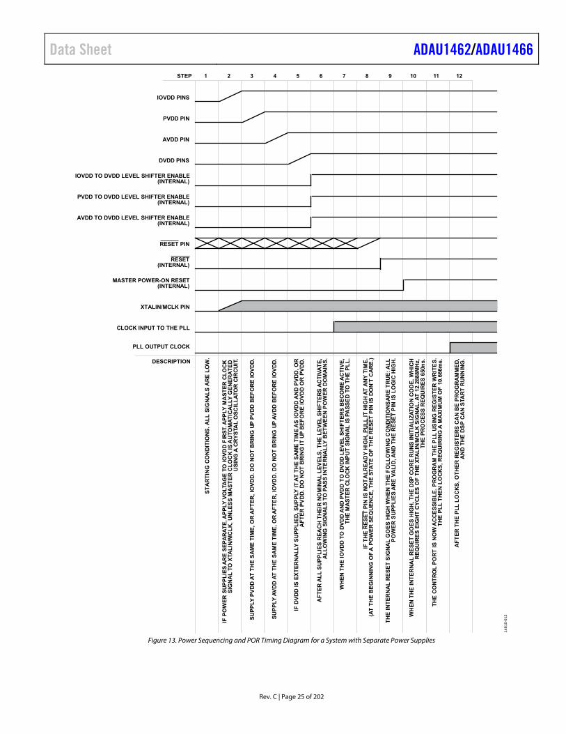
INITIALIZATION Power-Up Sequence
The first step in the initialization sequence is to power up the device. First, apply voltage to the power pins. All the power pins can be supplied simultaneously. If the power pins are not supplied simultaneously, supply IOVDD first because the internal ESD protection diodes are referenced to the IOVDD voltage. AVDD, DVDD, and PVDD can be supplied at the same time as IOVDD or after, but they must not be supplied prior to IOVDD. The order in which AVDD, DVDD, and PVDD are supplied does not matter.
DVDD, the power supply for the internal digital logic, can be regulated and supplied directly or it can by generated from IOVDD using an internal voltage regulator. When the internal regulator is not used and DVDD is directly supplied, no special sequence is required when providing the proper voltages to AVDD, DVDD, and PVDD.
When the internal regulator is used, DVDD is derived from IOVDD in combination with an external pass transistor, after AVDD, IOVDD, and PVDD are supplied. See the Power Supplies section for more information.
Each power supply domain has its own internal power-on reset (POR) circuits (also known as power OK circuits) to ensure that the level shifters attached to each power domain can be initialized properly. AVDD and PVDD must reach their nominal level before the auxiliary ADC and PLL can be used, respectively.
However, the AVDD and PVDD supplies have no role in the rest of the power-up sequence. After the AVDD power reaches its nominal threshold, the regulator becomes active and begins to charge up the DVDD supply. The DVDD supply also has a POR circuit to ensure that the level shifters initialize during power-up.
The POR signals are combined into three global level shifter resets that properly initialize the signal crossings between each separate power domain and DVDD.
The digital circuits remain in reset until the IOVDD to DVDD level shifter reset is released. At that point, the digital circuits exit reset.
When a crystal is in use, the crystal oscillator circuit must provide a stable master clock to the XTALIN/MCLK pin by the time the PVDD supply reaches its nominal level. The XTALIN/MCLK pin is restricted from passing into the PLL circuitry until the DVDD POR signal becomes active and the PVDD to DVDD level shifter is initialized.
When all four POR circuits signal that the power-on conditions are met, a reset synchronizer circuit releases the internal digital circuitry from reset, provided that the following conditions are met:
A valid MCLK signal is provided to the digital circuitry and the PLL.
The RESET pin is high.
When the internal digital circuitry becomes active, the DSP core runs eight lines of initialization code stored in read-only memory (ROM), requiring eight cycles of the MCLK signal. For a 12.288 MHz MCLK input, this process takes 650 ns.
After the ROM program completes its execution, the PLL is ready to be configured using register writes to Register 0xF000 (PLL_CTRL0), Register 0xF001 (PLL_CTRL1), Register 0xF002 (PLL_CLK_SRC), and Register 0xF003 (PLL_ENABLE).
When the PLL is configured and enabled, the PLL starts to lock to the incoming master clock signal. The absolute maximum PLL lock time is 32 × 1024 = 32,768 clock cycles on the clock signal (after the input prescaler), which is fed to the input of the PLL. In a standard 48 kHz use case, the PLL input clock frequency after the prescaler is 3.072 MHz; therefore, the maximum PLL lock time is 10.666 ms.
Typically, the PLL locks much faster than 10.666 ms. In most systems, the PLL locks within about 3.5 ms. The PLL_LOCK register (Address 0xF004) can be polled via the control port until Bit 0 (PLL_LOCK) goes high, signifying that the PLL lock is complete.
While the PLL is attempting to lock to the input clock, the I2C slave and SPI slave control ports are inactive; therefore, no other registers are accessible over the control port. While the PLL is attempting to lock, all attempts to write to the control port fail.
Figure 13 shows an example power-up sequence with all relevant signals labeled. If possible, apply the required voltage to all four power supply domains (IOVDD, AVDD, PVDD, and DVDD) simultaneously. If the power supplies are separate, IOVDD, which is the reference for the ESD protection diodes that are situated inside the input and output pins, must be applied first to avoid stressing these diodes. PVDD, AVDD, and DVDD can then be supplied in any order (see the System Initialization Sequence section for more information). Note that the gray areas in Figure 13 represent clock signals.
Data Sheet ADAU1462/ADAU1466
Rev. C | Page 25 of 202
STEP 1 2 3 4 5 6 7 8 9 10 11 12
IOVDD PINS
PVDD PIN
AVDD PIN
DVDD PINS
IOVDD TO DVDD LEVEL SHIFTER ENABLE(INTERNAL)
PVDD TO DVDD LEVEL SHIFTER ENABLE(INTERNAL)
AVDD TO DVDD LEVEL SHIFTER ENABLE(INTERNAL)
RESET PIN
RESET(INTERNAL)
MASTER POWER-ON RESET(INTERNAL)
XTALIN/MCLK PIN
CLOCK INPUT TO THE PLL
PLL OUTPUT CLOCK
DESCRIPTION
ST
AR
TIN
G C
ON
DIT
ION
S.
AL
L S
IGN
AL
S A
RE
LO
W.
IF P
OW
ER
SU
PP
LIE
SA
RE
SE
PA
RA
TE
,AP
PLY
VO
LTA
GE
TO
IO
VD
D F
IRS
T.A
PP
LY M
AS
TE
R C
LO
CK
SIG
NA
LT
O X
TAL
IN/M
CL
K,
UN
LE
SS
MA
ST
ER
CL
OC
K I
SA
UT
OM
AT
ICA
LLY
GE
NE
RA
TE
DU
SIN
G A
CR
YS
TAL
OS
CIL
LA
TO
R C
IRC
UIT
.
SU
PP
LY P
VD
DA
T T
HE
SA
ME
TIM
E,
OR
AF
TE
R,
IOV
DD
. D
O N
OT
BR
ING
UP
PV
DD
BE
FO
RE
IO
VD
D.
SU
PP
LYA
VD
DA
T T
HE
SA
ME
TIM
E,
OR
AF
TE
R,
IOV
DD
. D
O N
OT
BR
ING
UP
AV
DD
BE
FO
RE
IO
VD
D.
IF D
VD
D I
S E
XT
ER
NA
LLY
SU
PP
LIE
D,
SU
PP
LY I
TA
T T
HE
SA
ME
TIM
EA
S I
OV
DD
AN
D P
VD
D,
OR
AF
TE
R P
VD
D.
DO
NO
T B
RIN
G I
T U
P B
EF
OR
E I
OV
DD
OR
PV
DD
.
AF
TE
RA
LL
SU
PP
LIE
S R
EA
CH
TH
EIR
NO
MIN
AL
LE
VE
LS
, T
HE
LE
VE
L S
HIF
TE
RS
AC
TIV
AT
E,
AL
LO
WIN
G S
IGN
AL
ST
OP
AS
S I
NT
ER
NA
LLY
BE
TW
EE
N P
OW
ER
DO
MA
INS
.
WH
EN
TH
E I
OV
DD
TO
DV
DD
AN
D P
VD
DT
O D
VD
D L
EV
EL
SH
IFT
ER
S B
EC
OM
EA
CT
IVE
,T
HE
MA
ST
ER
CL
OC
K I
NP
UT
SIG
NA
L I
SP
AS
SE
DT
O T
HE
PL
L.
IF T
HE
RE
SE
T P
IN I
S N
OT
AL
RE
AD
Y H
IGH
, P
UL
L I
T H
IGH
AT
AN
Y T
IME
.(A
T T
HE
BE
GIN
NIN
G O
F A
PO
WE
R S
EQ
UE
NC
E,
TH
E S
TAT
E O
F T
HE
RE
SE
T P
IN I
S D
ON
’T C
AR
E.)
TH
E I
NT
ER
NA
L R
ES
ET
SIG
NA
L G
OE
S H
IGH
WH
EN
TH
E F
OL
LO
WIN
G C
ON
DIT
ION
SA
RE
TR
UE
:A
LL
PO
WE
R S
UP
PL
IES
AR
EV
AL
ID,A
ND
TH
E R
ES
ET
PIN
IS
LO
GIC
HIG
H.
WH
EN
TH
E I
NT
ER
NA
L R
ES
ET
GO
ES
HIG
H,
TH
E D
SP
CO
RE
RU
NS
IN
ITIA
LIZ
AT
ION
CO
DE
, W
HIC
HR
EQ
UIR
ES
EIG
HT
CY
CL
ES
OF
TH
E X
TAL
IN/M
CL
K S
IGN
AL
.AT
12.
2888
MH
z,T
HE
PR
OC
ES
S R
EQ
UIR
ES
650
ns.
TH
E C
ON
TR
OL
PO
RT
IS
NO
WA
CC
ES
SIB
LE
. P
RO
GR
AM
TH
E P
LL
US
ING
RE
GIS
TE
R W
RIT
ES
.T
HE
PL
L T
HE
N L
OC
KS
, R
EQ
UIR
ING
A M
AX
IMU
M O
F 1
0.66
6ms.
AF
TE
R T
HE
PL
L L
OC
KS
, O
TH
ER
RE
GIS
TE
RS
CA
N B
E P
RO
GR
AM
ME
D,
AN
D T
HE
DS
P C
AN
STA
RT
RU
NN
ING
.
148
10-0
13
Figure 13. Power Sequencing and POR Timing Diagram for a System with Separate Power Supplies
ADAU1462/ADAU1466 Data Sheet
Rev. C | Page 26 of 202
System Initialization Sequence
Before the IC can process the audio in the DSP, the following initialization sequence must be completed.
1. If possible, apply the required voltage to all four power supply domains (IOVDD, AVDD, PVDD, and DVDD) simultaneously. If simultaneous application is not possible, supply IOVDD first to prevent damage or reduced operating lifetime. If using the on-board regulator, AVDD and PVDD can be supplied in any order, and DVDD is then generated automatically. If not using the on-board regulator, AVDD, PVDD, and DVDD can be supplied in any order following IOVDD.
2. Start providing a master clock signal to the XTALIN/MCLK pin, or, if using the crystal oscillator, let the crystal oscillator start generating a master clock signal. The master clock signal must be valid when the DVDD supply stabilizes.
3. If the SELFBOOT pin is pulled high, a self boot sequence initiates on the master control port. Wait until the self boot operation is complete.
4. If SPI slave control mode is desired, toggle the SS/ADDR0 pin three times. Ensure that each toggle lasts at least the duration of one cycle of the master clock being input to the XTALIN/MCLK pin. When the SS/ADDR0 line rises for the third time, the slave control port is then in SPI mode.
5. Execute the register and memory write sequence that is required to configure the device in the proper operating mode.
Table 19 contains an example series of register writes used to configure the system at startup. The contents of the data column may vary depending on the system configuration. The configuration that is listed in Table 19 represents the default initialization sequence for project files generated in SigmaStudio.
Recommended Program/Parameter Loading Procedure
When writing large amounts of data to the program or parameter RAM in direct write mode (such as when downloading the initial contents of the RAMs from an external memory), use the hibernate register (Address 0xF400) to disable the processor core, thus preventing unpleasant noises from appearing at the audio output. When small amounts of data are transmitted during real-time operation of the DSP (such as when updating individual parameters), the software safeload mechanism can be used (see the Software Safeload section).
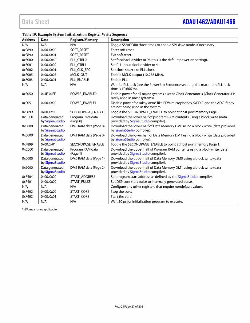
Data Sheet ADAU1462/ADAU1466
Rev. C | Page 27 of 202
Table 19. Example System Initialization Register Write Sequence1 Address Data Register/Memory Description N/A N/A N/A Toggle SS/ADDR0 three times to enable SPI slave mode, if necessary. 0xF890 0x00, 0x00 SOFT_RESET Enter soft reset. 0xF890 0x00, 0x01 SOFT_RESET Exit soft reset. 0xF000 0x00, 0x60 PLL_CTRL0 Set feedback divider to 96 (this is the default power-on setting). 0xF001 0x00, 0x02 PLL_CTRL1 Set PLL input clock divider to 4. 0xF002 0x00, 0x01 PLL_CLK_SRC Set clock source to PLL clock. 0xF005 0x00, 0x05 MCLK_OUT Enable MCLK output (12.288 MHz). 0xF003 0x00, 0x01 PLL_ENABLE Enable PLL. N/A N/A N/A Wait for PLL lock (see the Power-Up Sequence section); the maximum PLL lock
time is 10.666 ms. 0xF050 0x4F, 0xFF POWER_ENABLE0 Enable power for all major systems except Clock Generator 3 (Clock Generator 3 is
rarely used in most systems). 0xF051 0x00, 0x00 POWER_ENABLE1 Disable power for subsystems like PDM microphones, S/PDIF, and the ADC if they
are not being used in the system. 0xF899 0x00, 0x00 SECONDPAGE_ENABLE Toggle the SECONDPAGE_ENABLE to point at host port memory Page 0. 0xC000 Data generated
by SigmaStudio Program RAM data (Page 0)
Download the lower half of program RAM contents using a block write (data provided by SigmaStudio compiler).
0x0000 Data generated by SigmaStudio
DM0 RAM data (Page 0) Download the lower half of Data Memory DM0 using a block write (data provided by SigmaStudio compiler).
0x6000 Data generated by SigmaStudio
DM1 RAM data (Page 0) Download the lower half of Data Memory DM1 using a block write (data provided by SigmaStudio compiler).
0xF899 0x00,0x01 SECONDPAGE_ENABLE Toggle the SECONDPAGE_ENABLE to point at host port memory Page 1. 0xC000 Data generated
by SigmaStudio Program RAM data (Page 1)
Download the upper half of Program RAM contents using a block write (data provided by SigmaStudio compiler).
0x0000 Data generated by SigmaStudio
DM0 RAM data (Page 1) Download the upper half of Data Memory DM0 using a block write (data provided by SigmaStudio compiler).
0x6000 Data generated by SigmaStudio
DM1 RAM data (Page 2) Download the upper half of Data Memory DM1 using a block write (data provided by SigmaStudio compiler).
0xF404 0x00, 0x00 START_ADDRESS Set program start address as defined by the SigmaStudio compiler. 0xF401 0x00, 0x02 START_PULSE Set DSP core start pulse to internally generated pulse. N/A N/A N/A Configure any other registers that require nondefault values. 0xF402 0x00, 0x00 START_CORE Stop the core. 0xF402 0x00, 0x01 START_CORE Start the core. N/A N/A N/A Wait 50 μs for initialization program to execute. 1 N/A means not applicable.
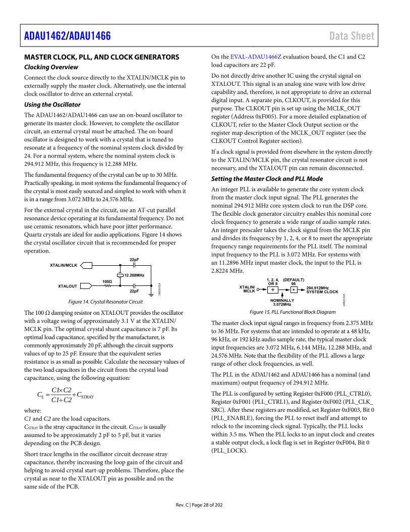
ADAU1462/ADAU1466 Data Sheet
Rev. C | Page 28 of 202
MASTER CLOCK, PLL, AND CLOCK GENERATORS Clocking Overview
Connect the clock source directly to the XTALIN/MCLK pin to externally supply the master clock. Alternatively, use the internal clock oscillator to drive an external crystal.
Using the Oscillator
The ADAU1462/ADAU1466 can use an on-board oscillator to generate its master clock. However, to complete the oscillator circuit, an external crystal must be attached. The on-board oscillator is designed to work with a crystal that is tuned to resonate at a frequency of the nominal system clock divided by 24. For a normal system, where the nominal system clock is 294.912 MHz, this frequency is 12.288 MHz.
The fundamental frequency of the crystal can be up to 30 MHz. Practically speaking, in most systems the fundamental frequency of the crystal is most easily sourced and simplest to work with when it is in a range from 3.072 MHz to 24.576 MHz.
For the external crystal in the circuit, use an AT-cut parallel resonance device operating at its fundamental frequency. Do not use ceramic resonators, which have poor jitter performance. Quartz crystals are ideal for audio applications. Figure 14 shows the crystal oscillator circuit that is recommended for proper operation.
100Ω
22pF
22pF
12.288MHz
XTALOUT
XTALIN/MCLK
14
81
0-0
14
Figure 14. Crystal Resonator Circuit
The 100 Ω damping resistor on XTALOUT provides the oscillator with a voltage swing of approximately 3.1 V at the XTALIN/ MCLK pin. The optimal crystal shunt capacitance is 7 pF. Its optimal load capacitance, specified by the manufacturer, is commonly approximately 20 pF, although the circuit supports values of up to 25 pF. Ensure that the equivalent series resistance is as small as possible. Calculate the necessary values of the two load capacitors in the circuit from the crystal load capacitance, using the following equation:
STRAYL CC2C1
C2C1C
where: C1 and C2 are the load capacitors. CSTRAY is the stray capacitance in the circuit. CSTRAY is usually assumed to be approximately 2 pF to 5 pF, but it varies depending on the PCB design.
Short trace lengths in the oscillator circuit decrease stray capacitance, thereby increasing the loop gain of the circuit and helping to avoid crystal start-up problems. Therefore, place the crystal as near to the XTALOUT pin as possible and on the same side of the PCB.
On the EVAL-ADAU1466Z evaluation board, the C1 and C2 load capacitors are 22 pF.
Do not directly drive another IC using the crystal signal on XTALOUT. This signal is an analog sine wave with low drive capability and, therefore, is not appropriate to drive an external digital input. A separate pin, CLKOUT, is provided for this purpose. The CLKOUT pin is set up using the MCLK_OUT register (Address 0xF005). For a more detailed explanation of CLKOUT, refer to the Master Clock Output section or the register map description of the MCLK_OUT register (see the CLKOUT Control Register section).
If a clock signal is provided from elsewhere in the system directly to the XTALIN/MCLK pin, the crystal resonator circuit is not necessary, and the XTALOUT pin can remain disconnected.
Setting the Master Clock and PLL Mode
An integer PLL is available to generate the core system clock from the master clock input signal. The PLL generates the nominal 294.912 MHz core system clock to run the DSP core. The flexible clock generator circuitry enables this nominal core clock frequency to generate a wide range of audio sample rates. An integer prescaler takes the clock signal from the MCLK pin and divides its frequency by 1, 2, 4, or 8 to meet the appropriate frequency range requirements for the PLL itself. The nominal input frequency to the PLL is 3.072 MHz. For systems with an 11.2896 MHz input master clock, the input to the PLL is 2.8224 MHz.
÷ ×
1, 2, 4,OR 8
XTALIN/MCLK
294.912MHzSYSTEM CLOCK
NOMINALLY3.072MHz
(DEFAULT)96
1481
0-01
5
Figure 15. PLL Functional Block Diagram
The master clock input signal ranges in frequency from 2.375 MHz to 36 MHz. For systems that are intended to operate at a 48 kHz, 96 kHz, or 192 kHz audio sample rate, the typical master clock input frequencies are 3.072 MHz, 6.144 MHz, 12.288 MHz, and 24.576 MHz. Note that the flexibility of the PLL allows a large range of other clock frequencies, as well.
The PLL in the ADAU1462 and ADAU1466 has a nominal (and maximum) output frequency of 294.912 MHz.
The PLL is configured by setting Register 0xF000 (PLL_CTRL0), Register 0xF001 (PLL_CTRL1), and Register 0xF002 (PLL_CLK_ SRC). After these registers are modified, set Register 0xF003, Bit 0 (PLL_ENABLE), forcing the PLL to reset itself and attempt to relock to the incoming clock signal. Typically, the PLL locks within 3.5 ms. When the PLL locks to an input clock and creates a stable output clock, a lock flag is set in Register 0xF004, Bit 0 (PLL_LOCK).
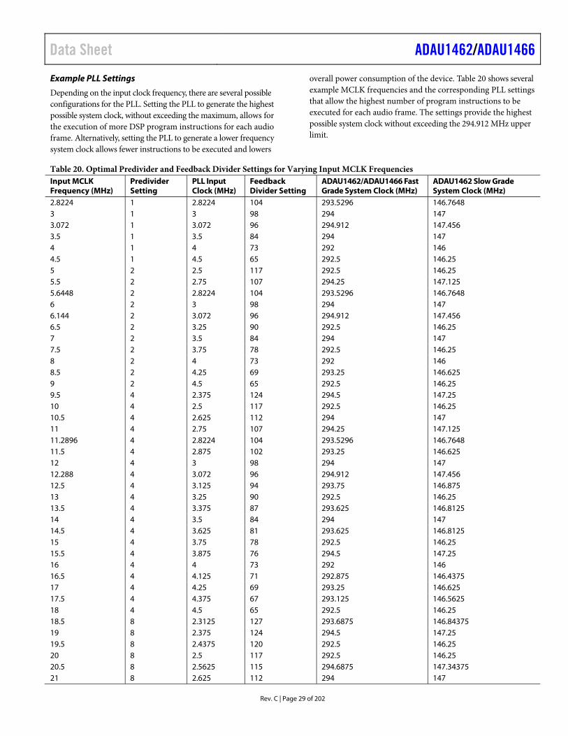
Data Sheet ADAU1462/ADAU1466
Rev. C | Page 29 of 202
Example PLL Settings
Depending on the input clock frequency, there are several possible configurations for the PLL. Setting the PLL to generate the highest possible system clock, without exceeding the maximum, allows for the execution of more DSP program instructions for each audio frame. Alternatively, setting the PLL to generate a lower frequency system clock allows fewer instructions to be executed and lowers
overall power consumption of the device. Table 20 shows several example MCLK frequencies and the corresponding PLL settings that allow the highest number of program instructions to be executed for each audio frame. The settings provide the highest possible system clock without exceeding the 294.912 MHz upper limit.
Table 20. Optimal Predivider and Feedback Divider Settings for Varying Input MCLK Frequencies Input MCLK Frequency (MHz)
Predivider Setting
PLL Input Clock (MHz)
Feedback Divider Setting
ADAU1462/ADAU1466 Fast Grade System Clock (MHz)
ADAU1462 Slow Grade System Clock (MHz)
2.8224 1 2.8224 104 293.5296 146.7648 3 1 3 98 294 147 3.072 1 3.072 96 294.912 147.456 3.5 1 3.5 84 294 147 4 1 4 73 292 146 4.5 1 4.5 65 292.5 146.25 5 2 2.5 117 292.5 146.25 5.5 2 2.75 107 294.25 147.125 5.6448 2 2.8224 104 293.5296 146.7648 6 2 3 98 294 147 6.144 2 3.072 96 294.912 147.456 6.5 2 3.25 90 292.5 146.25 7 2 3.5 84 294 147 7.5 2 3.75 78 292.5 146.25 8 2 4 73 292 146 8.5 2 4.25 69 293.25 146.625 9 2 4.5 65 292.5 146.25 9.5 4 2.375 124 294.5 147.25 10 4 2.5 117 292.5 146.25 10.5 4 2.625 112 294 147 11 4 2.75 107 294.25 147.125 11.2896 4 2.8224 104 293.5296 146.7648 11.5 4 2.875 102 293.25 146.625 12 4 3 98 294 147 12.288 4 3.072 96 294.912 147.456 12.5 4 3.125 94 293.75 146.875 13 4 3.25 90 292.5 146.25 13.5 4 3.375 87 293.625 146.8125 14 4 3.5 84 294 147 14.5 4 3.625 81 293.625 146.8125 15 4 3.75 78 292.5 146.25 15.5 4 3.875 76 294.5 147.25 16 4 4 73 292 146 16.5 4 4.125 71 292.875 146.4375 17 4 4.25 69 293.25 146.625 17.5 4 4.375 67 293.125 146.5625 18 4 4.5 65 292.5 146.25 18.5 8 2.3125 127 293.6875 146.84375 19 8 2.375 124 294.5 147.25 19.5 8 2.4375 120 292.5 146.25 20 8 2.5 117 292.5 146.25 20.5 8 2.5625 115 294.6875 147.34375 21 8 2.625 112 294 147
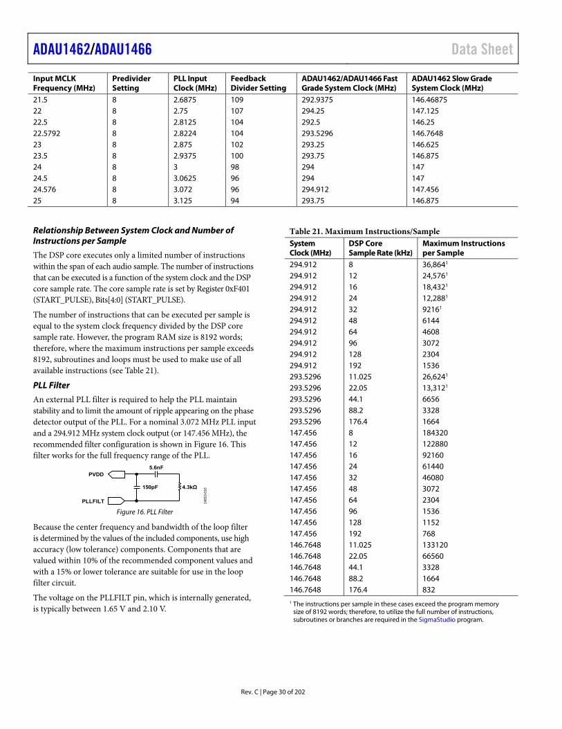
ADAU1462/ADAU1466 Data Sheet
Rev. C | Page 30 of 202
Input MCLK Frequency (MHz)
Predivider Setting
PLL Input Clock (MHz)
Feedback Divider Setting
ADAU1462/ADAU1466 Fast Grade System Clock (MHz)
ADAU1462 Slow Grade System Clock (MHz)
21.5 8 2.6875 109 292.9375 146.46875 22 8 2.75 107 294.25 147.125 22.5 8 2.8125 104 292.5 146.25 22.5792 8 2.8224 104 293.5296 146.7648 23 8 2.875 102 293.25 146.625 23.5 8 2.9375 100 293.75 146.875 24 8 3 98 294 147 24.5 8 3.0625 96 294 147 24.576 8 3.072 96 294.912 147.456 25 8 3.125 94 293.75 146.875
Relationship Between System Clock and Number of Instructions per Sample
The DSP core executes only a limited number of instructions within the span of each audio sample. The number of instructions that can be executed is a function of the system clock and the DSP core sample rate. The core sample rate is set by Register 0xF401 (START_PULSE), Bits[4:0] (START_PULSE).
The number of instructions that can be executed per sample is equal to the system clock frequency divided by the DSP core sample rate. However, the program RAM size is 8192 words; therefore, where the maximum instructions per sample exceeds 8192, subroutines and loops must be used to make use of all available instructions (see Table 21).
PLL Filter
An external PLL filter is required to help the PLL maintain stability and to limit the amount of ripple appearing on the phase detector output of the PLL. For a nominal 3.072 MHz PLL input and a 294.912 MHz system clock output (or 147.456 MHz), the recommended filter configuration is shown in Figure 16. This filter works for the full frequency range of the PLL.
5.6nF
150pF 4.3kΩ
PLLFILT
PVDD
1481
0-01
6
Figure 16. PLL Filter
Because the center frequency and bandwidth of the loop filter is determined by the values of the included components, use high accuracy (low tolerance) components. Components that are valued within 10% of the recommended component values and with a 15% or lower tolerance are suitable for use in the loop filter circuit.
The voltage on the PLLFILT pin, which is internally generated, is typically between 1.65 V and 2.10 V.
Table 21. Maximum Instructions/Sample System Clock (MHz)
DSP Core Sample Rate (kHz)
Maximum Instructions per Sample
294.912 8 36,8641 294.912 12 24,5761 294.912 16 18,4321 294.912 24 12,2881 294.912 32 92161 294.912 48 6144 294.912 64 4608 294.912 96 3072 294.912 128 2304 294.912 192 1536 293.5296 11.025 26,6241 293.5296 22.05 13,3121 293.5296 44.1 6656 293.5296 88.2 3328 293.5296 176.4 1664 147.456 8 184320 147.456 12 122880 147.456 16 92160 147.456 24 61440 147.456 32 46080 147.456 48 3072 147.456 64 2304 147.456 96 1536 147.456 128 1152 147.456 192 768 146.7648 11.025 133120 146.7648 22.05 66560 146.7648 44.1 3328 146.7648 88.2 1664 146.7648 176.4 832 1 The instructions per sample in these cases exceed the program memory
size of 8192 words; therefore, to utilize the full number of instructions, subroutines or branches are required in the SigmaStudio program.
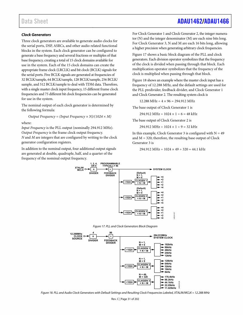
Data Sheet ADAU1462/ADAU1466
Rev. C | Page 31 of 202
Clock Generators
Three clock generators are available to generate audio clocks for the serial ports, DSP, ASRCs, and other audio related functional blocks in the system. Each clock generator can be configured to generate a base frequency and several fractions or multiples of that base frequency, creating a total of 15 clock domains available for use in the system. Each of the 15 clock domains can create the appropriate frame clock (LRCLK) and bit clock (BCLK) signals for the serial ports. Five BCLK signals are generated at frequencies of 32 BCLK/sample, 64 BCLK/sample, 128 BCLK/sample, 256 BCLK/ sample, and 512 BCLK/sample to deal with TDM data. Therefore, with a single master clock input frequency, 15 different frame clock frequencies and 75 different bit clock frequencies can be generated for use in the system.
The nominal output of each clock generator is determined by the following formula:
Output Frequency = (Input Frequency × N)/(1024 × M)
where: Input Frequency is the PLL output (nominally 294.912 MHz). Output Frequency is the frame clock output frequency. N and M are integers that are configured by writing to the clock generator configuration registers.
In addition to the nominal output, four additional output signals are generated at double, quadruple, half, and a quarter of the frequency of the nominal output frequency.
For Clock Generator 1 and Clock Generator 2, the integer numera-tor (N) and the integer denominator (M) are each nine bits long. For Clock Generator 3, N and M are each 16 bits long, allowing a higher precision when generating arbitrary clock frequencies.
Figure 17 shows a basic block diagram of the PLL and clock generators. Each division operator symbolizes that the frequency of the clock is divided when passing through that block. Each multiplication operator symbolizes that the frequency of the clock is multiplied when passing through that block.
Figure 18 shows an example where the master clock input has a frequency of 12.288 MHz, and the default settings are used for the PLL predivider, feedback divider, and Clock Generator 1 and Clock Generator 2. The resulting system clock is
12.288 MHz ÷ 4 × 96 = 294.912 MHz
The base output of Clock Generator 1 is
294.912 MHz ÷ 1024 × 1 ÷ 6 = 48 kHz
The base output of Clock Generator 2 is
294.912 MHz ÷ 1024 × 1 ÷ 9 = 32 kHz
In this example, Clock Generator 3 is configured with N = 49 and M = 320; therefore, the resulting base output of Clock Generator 3 is
294.912 MHz ÷ 1024 × 49 ÷ 320 = 44.1 kHz
×4
(Default)N = 1,M = 6
CLKGEN 1× N ÷ M÷1024
÷ ×
×4
(Default)N = 1,M = 9
CLKGEN 2× N ÷ M÷1024
×4
CLKGEN 3× N ÷ M÷1024
1, 2, 4,OR 8
DIVIDER
XTALIN/MCLK SYSTEM CLOCK
PROGRAMMABLETYPICALLY 96
FEEDBACKDIVIDER
×2×1÷2÷4
×2×1÷2÷4
×2×1÷2÷4 1
48
10
-01
7
Figure 17. PLL and Clock Generators Block Diagram
148
10-
01
8
192kHz96kHz48kHz24kHz12kHz
128kHz64kHz32kHz16kHz8kHz
176.4kHz88.2kHz44.1kHz22.05kHz11.025kHz
N = 1,M = 6
CLKGEN 1× N ÷ M÷1024
÷ ×
N = 1,M = 9
N = 49,M = 320
CLKGEN 2× N ÷ M÷1024
CLKGEN 3× N ÷ M÷1024
DIVIDER
12.288MHzCLOCK
SOURCE
964
FEEDBACKDIVIDER
294.912MHzSYSTEM CLOCK
Figure 18. PLL and Audio Clock Generators with Default Settings and Resulting Clock Frequencies Labeled, XTALIN/MCLK = 12.288 MHz
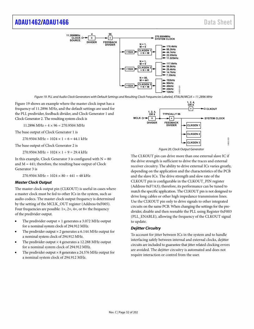
ADAU1462/ADAU1466 Data Sheet
Rev. C | Page 32 of 202
14
810
-01
9
192kHz96kHz48kHz24kHz12kHz
117.6kHz58.8kHz29.4kHz14.7kHz7.35kHz
176.4kHz88.2kHz44.1kHz22.05kHz11.025kHz
N = 1,M = 6
CLKGEN 1× N ÷ M÷1024
÷
N = 1,M = 9
N = 80,M = 441
CLKGEN 2× N ÷ M÷1024
CLKGEN 3× N ÷ M÷1024
DIVIDER
11.2896MHzCLOCK
SOURCE
4
FEEDBACKDIVIDER
270.9504MHzSYSTEM CLOCK×
96
Figure 19. PLL and Audio Clock Generators with Default Settings and Resulting Clock Frequencies Labeled, XTALIN/MCLK = 11.2896 MHz
Figure 19 shows an example where the master clock input has a frequency of 11.2896 MHz, and the default settings are used for the PLL predivider, feedback divider, and Clock Generator 1 and Clock Generator 2. The resulting system clock is
11.2896 MHz ÷ 4 × 96 = 270.9504 MHz
The base output of Clock Generator 1 is
270.9504 MHz ÷ 1024 × 1 ÷ 6 = 44.1 kHz
The base output of Clock Generator 2 is
270.9504 MHz ÷ 1024 × 1 ÷ 9 = 29.4 kHz
In this example, Clock Generator 3 is configured with N = 80 and M = 441; therefore, the resulting base output of Clock Generator 3 is
270.9504 MHz ÷ 1024 × 80 ÷ 441 = 48 kHz
Master Clock Output
The master clock output pin (CLKOUT) is useful in cases where a master clock must be fed to other ICs in the system, such as audio codecs. The master clock output frequency is determined by the setting of the MCLK_OUT register (Address 0xF005). Four frequencies are possible: 1×, 2×, 4×, or 8× the frequency of the predivider output.
The predivider output × 1 generates a 3.072 MHz output for a nominal system clock of 294.912 MHz.
The predivider output × 2 generates a 6.144 MHz output for a nominal system clock of 294.912 MHz.
The predivider output × 4 generates a 12.288 MHz output for a nominal system clock of 294.912 MHz.
The predivider output × 8 generates a 24.576 MHz output for a nominal system clock of 294.912 MHz.
CLKGEN 1
÷ ×
CLKGEN 2
CLKGEN 3
1, 2, 4,OR 8
1, 2, 4,OR 8
DIVIDER
MCLK SYSTEM CLOCK
TYPICALLY 96
×
FEEDBACKDIVIDER
CLKOUT
14
81
0-0
20
Figure 20. Clock Output Generator
The CLKOUT pin can drive more than one external slave IC if the drive strength is sufficient to drive the traces and external receiver circuitry. The ability to drive external ICs varies greatly, depending on the application and the characteristics of the PCB and the slave ICs. The drive strength and slew rate of the CLKOUT pin is configurable in the CLKOUT_PIN register (Address 0xF7A3); therefore, its performance can be tuned to match the specific application. The CLKOUT pin is not designed to drive long cables or other high impedance transmission lines. Use the CLKOUT pin only to drive signals to other integrated circuits on the same PCB. When changing the settings for the pre-divider, disable and then reenable the PLL using Register 0xF003 (PLL_ENABLE), allowing the frequency of the CLKOUT signal to update.
Dejitter Circuitry
To account for jitter between ICs in the system and to handle interfacing safely between internal and external clocks, dejitter circuits are included to guarantee that jitter related clocking errors are avoided. The dejitter circuitry is automated and does not require interaction or control from the user.
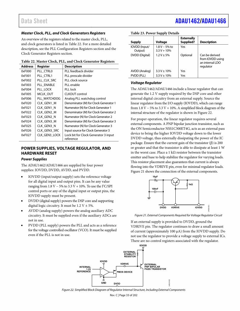
Data Sheet ADAU1462/ADAU1466
Rev. C | Page 33 of 202
Master Clock, PLL, and Clock Generators Registers
An overview of the registers related to the master clock, PLL, and clock generators is listed in Table 22. For a more detailed description, see the PLL Configuration Registers section and the Clock Generator Registers section.
Table 22. Master Clock, PLL, and Clock Generator Registers Address Register Description 0xF000 PLL_CTRL0 PLL feedback divider 0xF001 PLL_CTRL1 PLL prescale divider 0xF002 PLL_CLK_SRC PLL clock source 0xF003 PLL_ENABLE PLL enable 0xF004 PLL_LOCK PLL lock 0xF005 MCLK_OUT CLKOUT control 0xF006 PLL_WATCHDOG Analog PLL watchdog control 0xF020 CLK_GEN1_M Denominator (M) for Clock Generator 1 0xF021 CLK_GEN1_N Numerator (N) for Clock Generator 1 0xF022 CLK_GEN2_M Denominator (M) for Clock Generator 2 0xF023 CLK_GEN2_N Numerator (N) for Clock Generator 2 0xF024 CLK_GEN3_M Denominator (M) for Clock Generator 3 0xF025 CLK_GEN3_N Numerator (N) for Clock Generator 3 0xF026 CLK_GEN3_SRC Input source for Clock Generator 3 0xF027 CLK_GEN3_LOCK Lock bit for Clock Generator 3 input
reference
POWER SUPPLIES, VOLTAGE REGULATOR, AND HARDWARE RESET Power Supplies
The ADAU1462/ADAU1466 are supplied by four power supplies: IOVDD, DVDD, AVDD, and PVDD.
IOVDD (input/output supply) sets the reference voltage for all digital input and output pins. It can be any value ranging from 1.8 V − 5% to 3.3 V + 10%. To use the I2C/SPI control ports or any of the digital input or output pins, the IOVDD supply must be present.
DVDD (digital supply) powers the DSP core and supporting digital logic circuitry. It must be 1.2 V ± 5%.
AVDD (analog supply) powers the analog auxiliary ADC circuitry. It must be supplied even if the auxiliary ADCs are not in use.
PVDD (PLL supply) powers the PLL and acts as a reference for the voltage controlled oscillator (VCO). It must be supplied even if the PLL is not in use.
Table 23. Power Supply Details
Supply Voltage Externally Supplied? Description
IOVDD (Input/ Output)
1.8 V − 5% to 3.3 V + 10%
Yes
DVDD (Digital) 1.2 V ± 5% Optional Can be derived from IOVDD using an internal LDO regulator
AVDD (Analog) 3.3 V ± 10% Yes PVDD (PLL) 3.3 V ± 10% Yes
Voltage Regulator
The ADAU1462/ADAU1466 include a linear regulator that can generate the 1.2 V supply required by the DSP core and other internal digital circuitry from an external supply. Source the linear regulator from the I/O supply (IOVDD), which can range from 1.8 V − 5% to 3.3 V + 10%. A simplified block diagram of the internal structure of the regulator is shown in Figure 22.
For proper operation, the linear regulator requires several external components. A PNP bipolar junction transistor, such as the ON Semiconductor NSS1C300ET4G, acts as an external pass device to bring the higher IOVDD voltage down to the lower DVDD voltage, thus externally dissipating the power of the IC package. Ensure that the current gain of the transistor (β) is 200 or greater and that the transistor is able to dissipate at least 1 W in the worst case. Place a 1 kΩ resistor between the transistor emitter and base to help stabilize the regulator for varying loads. This resistor placement also guarantees that current is always flowing into the VDRIVE pin, even for minimal regulator loads. Figure 21 shows the connection of the external components.
1kΩ
VDRIVE IOVDDDVDD
10µF
100nF
+
1481
0-02
1
Figure 21. External Components Required for Voltage Regulator Circuit
If an external supply is provided to DVDD, ground the VDRIVE pin. The regulator continues to draw a small amount of current (approximately 100 μA) from the IOVDD supply. Do not use the regulator to provide a voltage supply to external ICs. There are no control registers associated with the regulator.
INTERNAL1.2V
REFERENCE PMOS DEVICE
VDRIVE
EXTERNALSTABILITYRESISTOR
EXTERNALPNP BIPOLARPASS TRANSISTOR
14
81
0-0
22
Figure 22. Simplified Block Diagram of Regulator Internal Structure, Including External Components
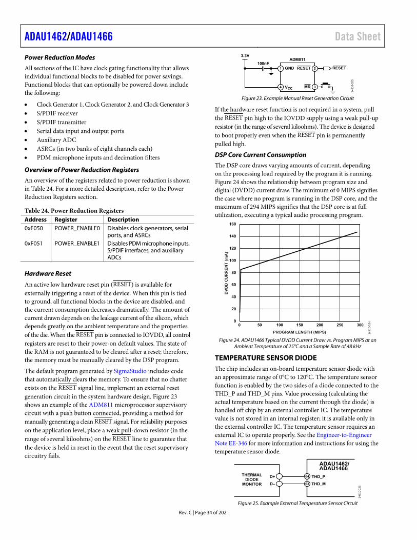
ADAU1462/ADAU1466 Data Sheet
Rev. C | Page 34 of 202
Power Reduction Modes
All sections of the IC have clock gating functionality that allows individual functional blocks to be disabled for power savings. Functional blocks that can optionally be powered down include the following:
Clock Generator 1, Clock Generator 2, and Clock Generator 3 S/PDIF receiver S/PDIF transmitter Serial data input and output ports Auxiliary ADC ASRCs (in two banks of eight channels each) PDM microphone inputs and decimation filters
Overview of Power Reduction Registers
An overview of the registers related to power reduction is shown in Table 24. For a more detailed description, refer to the Power Reduction Registers section.
Table 24. Power Reduction Registers Address Register Description 0xF050 POWER_ENABLE0 Disables clock generators, serial
ports, and ASRCs 0xF051 POWER_ENABLE1 Disables PDM microphone inputs,
S/PDIF interfaces, and auxiliary ADCs
Hardware Reset
An active low hardware reset pin (RESET) is available for externally triggering a reset of the device. When this pin is tied to ground, all functional blocks in the device are disabled, and the current consumption decreases dramatically. The amount of current drawn depends on the leakage current of the silicon, which depends greatly on the ambient temperature and the properties of the die. When the RESET pin is connected to IOVDD, all control registers are reset to their power-on default values. The state of the RAM is not guaranteed to be cleared after a reset; therefore, the memory must be manually cleared by the DSP program.
The default program generated by SigmaStudio includes code that automatically clears the memory. To ensure that no chatter exists on the RESET signal line, implement an external reset generation circuit in the system hardware design. Figure 23 shows an example of the ADM811 microprocessor supervisory circuit with a push button connected, providing a method for manually generating a clean RESET signal. For reliability purposes on the application level, place a weak pull-down resistor (in the range of several kiloohms) on the RESET line to guarantee that the device is held in reset in the event that the reset supervisory circuitry fails.
VCC MR
GND RESET
ADM8113.3V
RESET100nF
3
21
4
1481
0-02
3
Figure 23. Example Manual Reset Generation Circuit
If the hardware reset function is not required in a system, pull the RESET pin high to the IOVDD supply using a weak pull-up resistor (in the range of several kiloohms). The device is designed to boot properly even when the RESET pin is permanently pulled high.
DSP Core Current Consumption
The DSP core draws varying amounts of current, depending on the processing load required by the program it is running. Figure 24 shows the relationship between program size and digital (DVDD) current draw. The minimum of 0 MIPS signifies the case where no program is running in the DSP core, and the maximum of 294 MIPS signifies that the DSP core is at full utilization, executing a typical audio processing program.
0 50 100 150 200 250 300
DV
DD
CU
RR
EN
T (
mA
)
PROGRAM LENGTH (MIPS) 14
81
0-0
24
Figure 24. ADAU1466 Typical DVDD Current Draw vs. Program MIPS at an
Ambient Temperature of 25°C and a Sample Rate of 48 kHz
TEMPERATURE SENSOR DIODE The chip includes an on-board temperature sensor diode with an approximate range of 0°C to 120°C. The temperature sensor function is enabled by the two sides of a diode connected to the THD_P and THD_M pins. Value processing (calculating the actual temperature based on the current through the diode) is handled off chip by an external controller IC. The temperature value is not stored in an internal register; it is available only in the external controller IC. The temperature sensor requires an external IC to operate properly. See the Engineer-to-Engineer Note EE-346 for more information and instructions for using the temperature sensor diode.
1481
0-02
5
THERMALDIODE
MONITOR
ADAU1462/ADAU1466
D+
D–
THD_P
THD_M
64
63
Figure 25. Example External Temperature Sensor Circuit
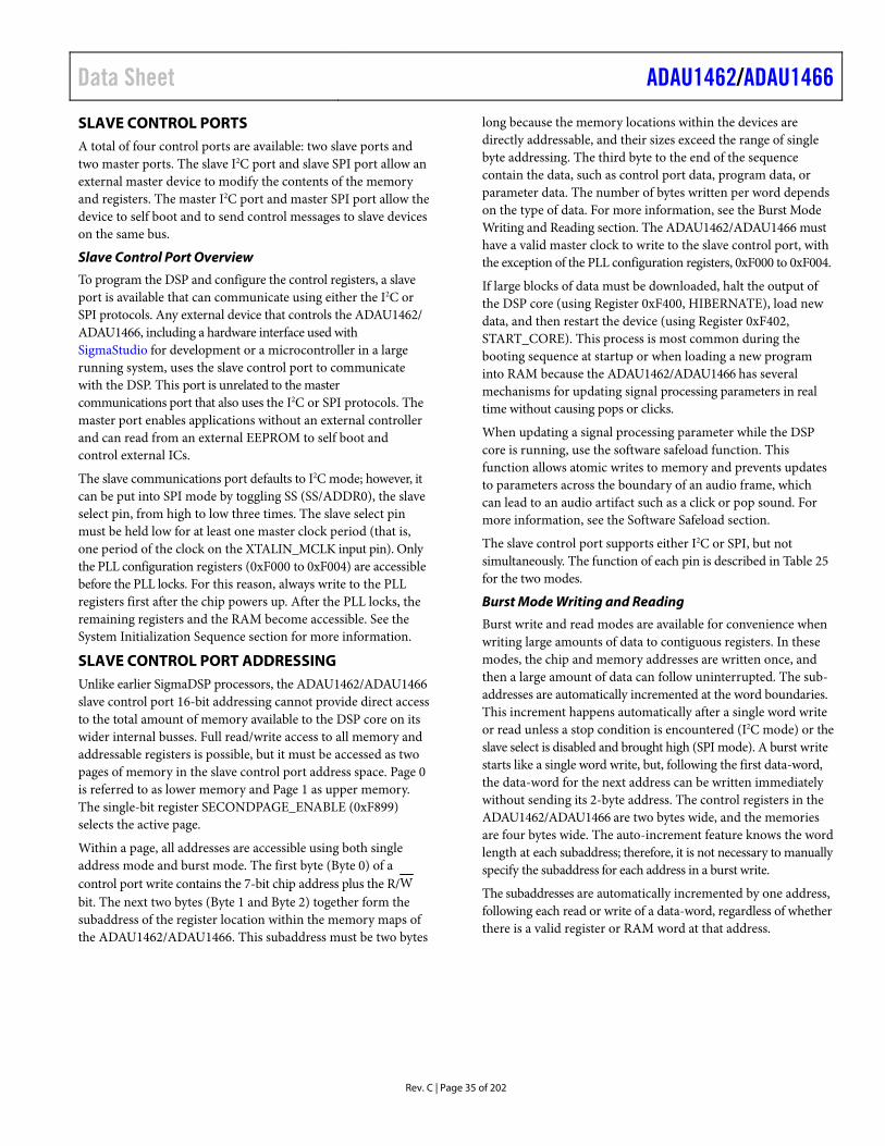
Data Sheet ADAU1462/ADAU1466
Rev. C | Page 35 of 202
SLAVE CONTROL PORTS A total of four control ports are available: two slave ports and two master ports. The slave I2C port and slave SPI port allow an external master device to modify the contents of the memory and registers. The master I2C port and master SPI port allow the device to self boot and to send control messages to slave devices on the same bus.
Slave Control Port Overview
To program the DSP and configure the control registers, a slave port is available that can communicate using either the I2C or SPI protocols. Any external device that controls the ADAU1462/ ADAU1466, including a hardware interface used with SigmaStudio for development or a microcontroller in a large running system, uses the slave control port to communicate with the DSP. This port is unrelated to the master communications port that also uses the I2C or SPI protocols. The master port enables applications without an external controller and can read from an external EEPROM to self boot and control external ICs.
The slave communications port defaults to I2C mode; however, it can be put into SPI mode by toggling SS (SS/ADDR0), the slave select pin, from high to low three times. The slave select pin must be held low for at least one master clock period (that is, one period of the clock on the XTALIN_MCLK input pin). Only the PLL configuration registers (0xF000 to 0xF004) are accessible before the PLL locks. For this reason, always write to the PLL registers first after the chip powers up. After the PLL locks, the remaining registers and the RAM become accessible. See the System Initialization Sequence section for more information.
SLAVE CONTROL PORT ADDRESSING Unlike earlier SigmaDSP processors, the ADAU1462/ADAU1466 slave control port 16-bit addressing cannot provide direct access to the total amount of memory available to the DSP core on its wider internal busses. Full read/write access to all memory and addressable registers is possible, but it must be accessed as two pages of memory in the slave control port address space. Page 0 is referred to as lower memory and Page 1 as upper memory. The single-bit register SECONDPAGE_ENABLE (0xF899) selects the active page.
Within a page, all addresses are accessible using both single address mode and burst mode. The first byte (Byte 0) of a control port write contains the 7-bit chip address plus the R/W bit. The next two bytes (Byte 1 and Byte 2) together form the subaddress of the register location within the memory maps of the ADAU1462/ADAU1466. This subaddress must be two bytes
long because the memory locations within the devices are directly addressable, and their sizes exceed the range of single byte addressing. The third byte to the end of the sequence contain the data, such as control port data, program data, or parameter data. The number of bytes written per word depends on the type of data. For more information, see the Burst Mode Writing and Reading section. The ADAU1462/ADAU1466 must have a valid master clock to write to the slave control port, with the exception of the PLL configuration registers, 0xF000 to 0xF004.
If large blocks of data must be downloaded, halt the output of the DSP core (using Register 0xF400, HIBERNATE), load new data, and then restart the device (using Register 0xF402, START_CORE). This process is most common during the booting sequence at startup or when loading a new program into RAM because the ADAU1462/ADAU1466 has several mechanisms for updating signal processing parameters in real time without causing pops or clicks.
When updating a signal processing parameter while the DSP core is running, use the software safeload function. This function allows atomic writes to memory and prevents updates to parameters across the boundary of an audio frame, which can lead to an audio artifact such as a click or pop sound. For more information, see the Software Safeload section.
The slave control port supports either I2C or SPI, but not simultaneously. The function of each pin is described in Table 25 for the two modes.
Burst Mode Writing and Reading
Burst write and read modes are available for convenience when writing large amounts of data to contiguous registers. In these modes, the chip and memory addresses are written once, and then a large amount of data can follow uninterrupted. The sub-addresses are automatically incremented at the word boundaries. This increment happens automatically after a single word write or read unless a stop condition is encountered (I2C mode) or the slave select is disabled and brought high (SPI mode). A burst write starts like a single word write, but, following the first data-word, the data-word for the next address can be written immediately without sending its 2-byte address. The control registers in the ADAU1462/ADAU1466 are two bytes wide, and the memories are four bytes wide. The auto-increment feature knows the word length at each subaddress; therefore, it is not necessary to manually specify the subaddress for each address in a burst write.
The subaddresses are automatically incremented by one address, following each read or write of a data-word, regardless of whether there is a valid register or RAM word at that address.
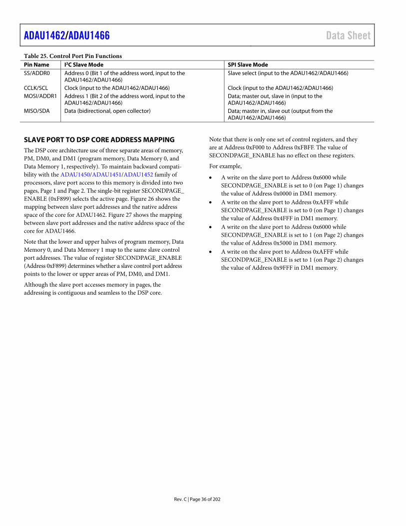
ADAU1462/ADAU1466 Data Sheet
Rev. C | Page 36 of 202
Table 25. Control Port Pin Functions Pin Name I2C Slave Mode SPI Slave Mode SS/ADDR0 Address 0 (Bit 1 of the address word, input to the
ADAU1462/ADAU1466) Slave select (input to the ADAU1462/ADAU1466)
CCLK/SCL Clock (input to the ADAU1462/ADAU1466) Clock (input to the ADAU1462/ADAU1466) MOSI/ADDR1 Address 1 (Bit 2 of the address word, input to the
ADAU1462/ADAU1466) Data; master out, slave in (input to the ADAU1462/ADAU1466)
MISO/SDA Data (bidirectional, open collector) Data; master in, slave out (output from the ADAU1462/ADAU1466)
SLAVE PORT TO DSP CORE ADDRESS MAPPING The DSP core architecture use of three separate areas of memory, PM, DM0, and DM1 (program memory, Data Memory 0, and Data Memory 1, respectively). To maintain backward compati-bility with the ADAU1450/ADAU1451/ADAU1452 family of processors, slave port access to this memory is divided into two pages, Page 1 and Page 2. The single-bit register SECONDPAGE_ ENABLE (0xF899) selects the active page. Figure 26 shows the mapping between slave port addresses and the native address space of the core for ADAU1462. Figure 27 shows the mapping between slave port addresses and the native address space of the core for ADAU1466.
Note that the lower and upper halves of program memory, Data Memory 0, and Data Memory 1 map to the same slave control port addresses. The value of register SECONDPAGE_ENABLE (Address 0xF899) determines whether a slave control port address points to the lower or upper areas of PM, DM0, and DM1.
Although the slave port accesses memory in pages, the addressing is contiguous and seamless to the DSP core.
Note that there is only one set of control registers, and they are at Address 0xF000 to Address 0xFBFF. The value of SECONDPAGE_ENABLE has no effect on these registers.
For example,
A write on the slave port to Address 0x6000 while SECONDPAGE_ENABLE is set to 0 (on Page 1) changes the value of Address 0x0000 in DM1 memory.
A write on the slave port to Address 0xAFFF while SECONDPAGE_ENABLE is set to 0 (on Page 1) changes the value of Address 0x4FFF in DM1 memory.
A write on the slave port to Address 0x6000 while SECONDPAGE_ENABLE is set to 1 (on Page 2) changes the value of Address 0x5000 in DM1 memory.
A write on the slave port to Address 0xAFFF while SECONDPAGE_ENABLE is set to 1 (on Page 2) changes the value of Address 0x9FFF in DM1 memory.
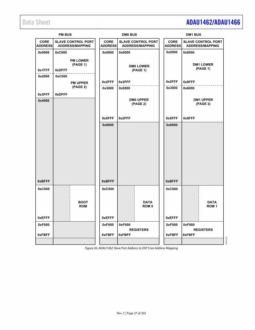
Data Sheet ADAU1462/ADAU1466
Rev. C | Page 37 of 202
148
10-1
26
DM0 BUS
DM0 LOWER(PAGE 1)
DM0 UPPER(PAGE 2)
REGISTERS
DATAROM 0
0xC000
0xEFFF
0xF000
0xFBFF
0xBFFF
0x6000
0x8FFF
COREADDRESS
SLAVE CONTROL PORTADDRESS/MAPPING
DM1 BUS
0x5FFF
0x6000
DM1 LOWER(PAGE 1)
DM1 UPPER(PAGE 2)
REGISTERS
DATAROM 1
0xC000
0xEFFF
0xF000
0xFBFF
0xF000
0xFBFF
0xF000
0xFBFF
0xBFFF
0x6000
0x8FFF
COREADDRESS
SLAVE CONTROL PORTADDRESS/MAPPING
PM BUS
0x0000 0xC000
0x3FFF
0x4000
0xDFFF
COREADDRESS
SLAVE CONTROL PORTADDRESS/MAPPING
0x1FFF
0xC000
PM LOWER(PAGE 1)
PM UPPER(PAGE 2)
0xDFFF
0x2000
BOOTROM
0xC000
0xF000
0xFBFF
0xBFFF
0xEFFF
0x0000
0x2FFF
0x0000
0x0000
0x2FFF
0x3000
0x0000
0x2FFF
0x3000
0x5FFF
0x6000
0x2FFF
Figure 26. ADAU1462 Slave Port Address to DSP Core Address Mapping
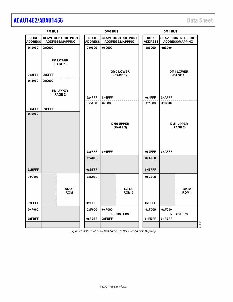
ADAU1462/ADAU1466 Data Sheet
Rev. C | Page 38 of 202
14
810-
12
7
DM0 BUS
0x0000
0x4FFF
0x5000
DM0 LOWER(PAGE 1)
DM0 UPPER(PAGE 2)
REGISTERS
DATAROM 0
0xC000
0xEFFF
0xF000
0xFBFF
0xBFFF
0xA000
0x9FFF
0x0000
0x4FFF
0x0000
0x4FFF
COREADDRESS
SLAVE CONTROL PORTADDRESS/MAPPING
DM1 BUS
0x0000
0x4FFF
0x5000
DM1 LOWER(PAGE 1)
DM1 UPPER(PAGE 2)
REGISTERS
DATAROM 1
0xC000
0xEFFF
0xF000
0xFBFF
0xF000
0xFBFF
0xF000
0xFBFF
0xBFFF
0xA000
0x9FFF
0x6000
0xAFFF
0x6000
0xAFFF
COREADDRESS
SLAVE CONTROL PORTADDRESS/MAPPING
PM BUS
0x0000
0x2FFF
0xC000
0xC000
PM LOWER(PAGE 1)
PM UPPER(PAGE 2)
0xEFFF
0x3000
BOOTROM
0x5FFF
0xC000
0xF000
0xFBFF
0xBFFF
0x6000
0xEFFF
0xEFFF
COREADDRESS
SLAVE CONTROL PORTADDRESS/MAPPING
Figure 27. ADAU1466 Slave Port Address to DSP Core Address Mapping
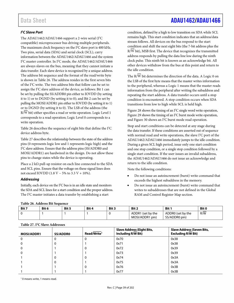
Data Sheet ADAU1462/ADAU1466
Rev. C | Page 39 of 202
I2C Slave Port
The ADAU1462/ADAU1466 support a 2-wire serial (I2C compatible) microprocessor bus driving multiple peripherals. The maximum clock frequency on the I2C slave port is 400 kHz. Two pins, serial data (SDA) and serial clock (SCL), carry information between the ADAU1462/ADAU1466 and the system I2C master controller. In I2C mode, the ADAU1462/ADAU1466 are always slaves on the bus, meaning that they cannot initiate a data transfer. Each slave device is recognized by a unique address. The address bit sequence and the format of the read/write byte is shown in Table 26. The address resides in the first seven bits of the I2C write. The two address bits that follow can be set to assign the I2C slave address of the device, as follows: Bit 1 can be set by pulling the SS/ADDR0 pin either to IOVDD (by setting it to 1) or to DGND (by setting it to 0); and Bit 2 can be set by pulling the MOSI/ADDR1 pin either to IOVDD (by setting it to 1) or to DGND (by setting it to 0). The LSB of the address (the R/W bit) either specifies a read or write operation. Logic Level 1 corresponds to a read operation; Logic Level 0 corresponds to a write operation.
Table 26 describes the sequence of eight bits that define the I2C device address byte.
Table 27 describes the relationship between the state of the address pins (0 represents logic low and 1 represents logic high) and the I2C slave address. Ensure that the address pins (SS/ADDR0 and MOSI/ADDR1) are hardwired in the design. Do not allow these pins to change states while the device is operating.
Place a 2 kΩ pull-up resistor on each line connected to the SDA and SCL pins. Ensure that the voltage on these signal lines does not exceed IOVDD (1.8 V − 5% to 3.3 V + 10%).
Addressing
Initially, each device on the I2C bus is in an idle state and monitors the SDA and SCL lines for a start condition and the proper address. The I2C master initiates a data transfer by establishing a start
condition, defined by a high to low transition on SDA while SCL remains high. This start condition indicates that an address/data stream follows. All devices on the bus respond to the start condition and shift the next eight bits (the 7-bit address plus the R/W bit), MSB first. The device that recognizes the transmitted address responds by pulling the data line low during the ninth clock pulse. This ninth bit is known as an acknowledge bit. All other devices withdraw from the bus at this point and return to the idle condition.
The R/W bit determines the direction of the data. A Logic 0 on the LSB of the first byte means that the master writes information to the peripheral, whereas a Logic 1 means that the master reads information from the peripheral after writing the subaddress and repeating the start address. A data transfer occurs until a stop condition is encountered. A stop condition occurs when SDA transitions from low to high while SCL is held high.
Figure 28 shows the timing of an I2C single word write operation, Figure 29 shows the timing of an I2C burst mode write operation, and Figure 30 shows an I2C burst mode read operation.
Stop and start conditions can be detected at any stage during the data transfer. If these conditions are asserted out of sequence with normal read and write operations, the slave I2C port of the ADAU1462/ADAU1466 immediately jumps to the idle condition. During a given SCL high period, issue only one start condition and one stop condition, or a single stop condition followed by a single start condition. If the user issues an invalid subaddress, the ADAU1462/ADAU1466 do not issue an acknowledge and return to the idle condition.
Note the following conditions:
Do not issue an autoincrement (burst) write command that exceeds the highest subaddress in the memory.
Do not issue an autoincrement (burst) write command that writes to subaddresses that are not defined in the Global RAM and Control Register Map section.
Table 26. Address Bit Sequence Bit 7 Bit 6 Bit 5 Bit 4 Bit 3 Bit 2 Bit 1 Bit 0 0 1 1 1 0 ADDR1 (set by the
MOSI/ADDR1 pin) ADDR0 (set by the SS/ADDR0 pin)
R/W
Table 27. I2C Slave Addresses
MOSI/ADDR1 SS/ADDR0 Read/Write1 Slave Address (Eight Bits, Including R/W Bit)
Slave Address (Seven Bits, Excluding R/W Bit)
0 0 0 0x70 0x38 0 0 1 0x71 0x38 0 1 0 0x72 0x39 0 1 1 0x73 0x39 1 0 0 0x74 0x3A 1 0 1 0x75 0x3A 1 1 0 0x76 0x3B 1 1 1 0x77 0x3B 1 0 means write, 1 means read.
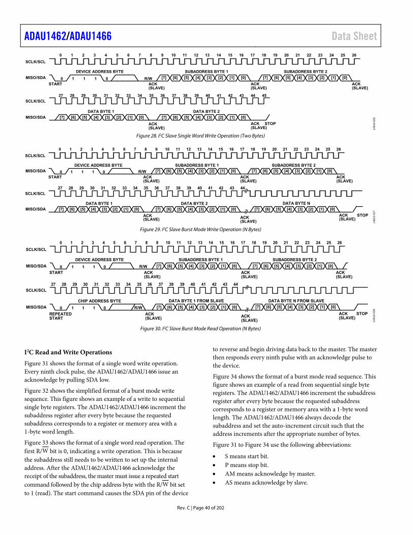
ADAU1462/ADAU1466 Data Sheet
Rev. C | Page 40 of 202
[7] [6] [5] [4] [3] [2] [1] [0] [7] [6] [5] [4] [3] [2] [1] [0]
[7] [6] [5] [4] [3] [2] [1] [0][7] [6] [5] [4] [3] [2] [1] [0]
STOP
DATA BYTE 1 DATA BYTE 2
0 1 2 3 4 5 6 7 8 9 10 11 12 13 14 15 16 17 18 19 2120 22 23 24 25 26
27 28 29 3130 32 33 34 35 36 37 38 39 4140 42 43 44 45
0 1 1 1 0 R/W
DEVICE ADDRESS BYTE SUBADDRESS BYTE 1 SUBADDRESS BYTE 2
ACK(SLAVE)
ACK(SLAVE)
ACK(SLAVE)
ACK(SLAVE)
ACK(SLAVE)
START
SCLK/SCL
MISO/SDA
SCLK/SCL
MISO/SDA
1481
0-02
6
Figure 28. I2C Slave Single Word Write Operation (Two Bytes)
[7] [6] [5] [4] [3] [2] [1] [0] [7] [6] [5] [4] [3] [2] [1] [0]
[7] [6] [5] [4] [3] [2] [1] [0][7] [6] [5] [4] [3] [2] [1] [0]
DATA BYTE 1 DATA BYTE 2
0 1 2 3 4 5 6 7 8 9 10 11 12 13 14 15 16 17 18 19 2120 22 23 24 25 26
27 28 29 3130 32 33 34 35 36 37 38 39 4140 42 43 44
0 1 1 1 0 R/W
DEVICE ADDRESS BYTE SUBADDRESS BYTE 1 SUBADDRESS BYTE 2
ACK(SLAVE)
[7] [6] [5] [4] [3] [2] [1] [0]
DATA BYTE N
ACK(SLAVE)
STOP
ACK(SLAVE)
ACK(SLAVE)
ACK(SLAVE) ACK
(SLAVE)
START
SCLK/SCL
MISO/SDA
SCLK/SCL
MISO/SDA
14
81
0-0
27
Figure 29. I2C Slave Burst Mode Write Operation (N Bytes)
[7] [6] [5] [4] [3] [2] [1] [0]
[7] [6] [5] [4] [3] [2] [1] [0][7] [6] [5] [4] [3] [2] [1] [0]
CHIP ADDRESS BYTE DATA BYTE 1 FROM SLAVE
0 1 2 3 4 5 6 7 8 9 10 11 12 13 14 15 16 17 18 19 2120 22 23 24 25 26
27 28 29 3130 32 33 34 35 36 37 38 39 4140 42 43 44
0 1 1 1 0 R/W
0 1 1 1 0 R/W
DEVICE ADDRESS BYTE SUBADDRESS BYTE 1 SUBADDRESS BYTE 2
ACK(SLAVE)
STOP
[7] [6] [5] [4] [3] [2] [1] [0]
DATA BYTE N FROM SLAVE
ACK(SLAVE)
ACK(SLAVE)
ACK(SLAVE)
ACK(SLAVE) ACK
(SLAVE)
START
REPEATEDSTART
SCLK/SCL
MISO/SDA
SCLK/SCL
MISO/SDA
14
81
0-0
28
Figure 30. I2C Slave Burst Mode Read Operation (N Bytes)
I2C Read and Write Operations
Figure 31 shows the format of a single word write operation. Every ninth clock pulse, the ADAU1462/ADAU1466 issue an acknowledge by pulling SDA low.
Figure 32 shows the simplified format of a burst mode write sequence. This figure shows an example of a write to sequential single byte registers. The ADAU1462/ADAU1466 increment the subaddress register after every byte because the requested subaddress corresponds to a register or memory area with a 1-byte word length.
Figure 33 shows the format of a single word read operation. The first R/W bit is 0, indicating a write operation. This is because the subaddress still needs to be written to set up the internal address. After the ADAU1462/ADAU1466 acknowledge the receipt of the subaddress, the master must issue a repeated start command followed by the chip address byte with the R/W bit set to 1 (read). The start command causes the SDA pin of the device
to reverse and begin driving data back to the master. The master then responds every ninth pulse with an acknowledge pulse to the device.
Figure 34 shows the format of a burst mode read sequence. This figure shows an example of a read from sequential single byte registers. The ADAU1462/ADAU1466 increment the subaddress register after every byte because the requested subaddress corresponds to a register or memory area with a 1-byte word length. The ADAU1462/ADAU1466 always decode the subaddress and set the auto-increment circuit such that the address increments after the appropriate number of bytes.
Figure 31 to Figure 34 use the following abbreviations:
S means start bit. P means stop bit. AM means acknowledge by master. AS means acknowledge by slave.
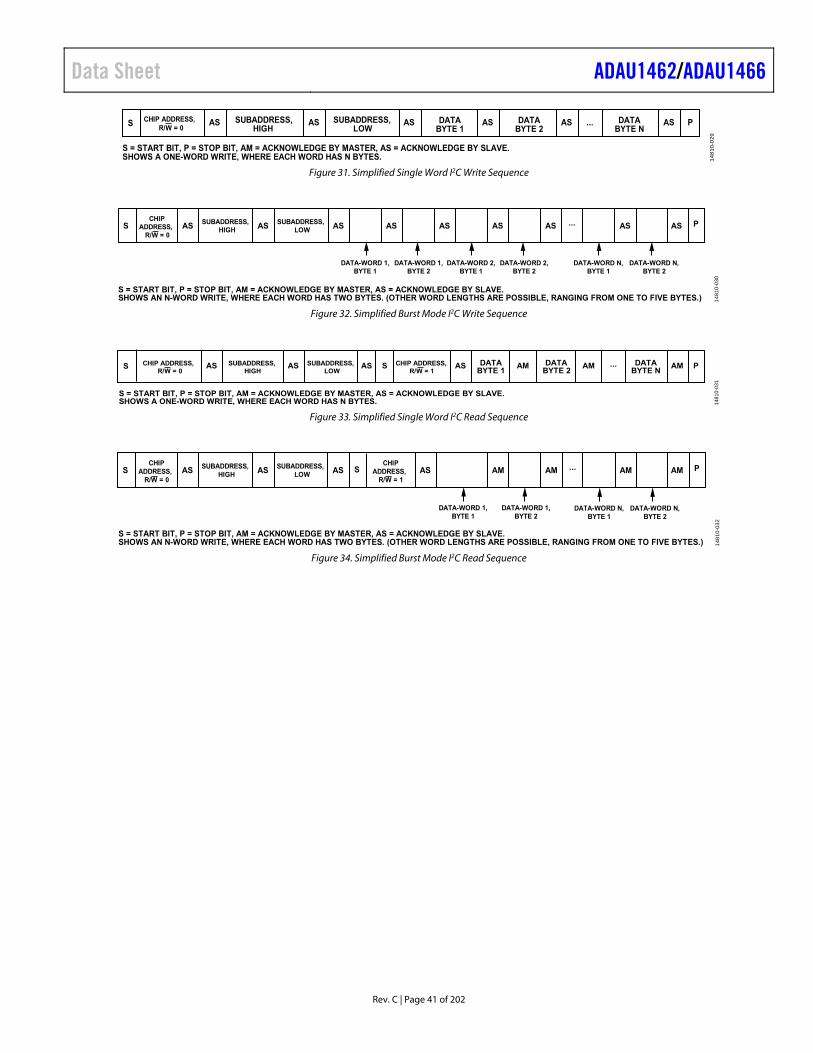
Data Sheet ADAU1462/ADAU1466
Rev. C | Page 41 of 202
S AS SUBADDRESS,LOW
AS AS AS AS ... AS PCHIP ADDRESS,R/W = 0
DATABYTE 1
DATABYTE 2
DATABYTE N
SUBADDRESS,HIGH
S = START BIT, P = STOP BIT, AM = ACKNOWLEDGE BY MASTER, AS = ACKNOWLEDGE BY SLAVE.SHOWS A ONE-WORD WRITE, WHERE EACH WORD HAS N BYTES. 1
48
10
-02
9
Figure 31. Simplified Single Word I2C Write Sequence
S AS AS AS AS AS AS AS AS AS... PCHIP
ADDRESS,R/W = 0
SUBADDRESS,HIGH
SUBADDRESS,LOW
DATA-WORD 1,BYTE 1
DATA-WORD 1,BYTE 2
DATA-WORD 2,BYTE 1
DATA-WORD 2,BYTE 2
DATA-WORD N,BYTE 1
DATA-WORD N,BYTE 2
S = START BIT, P = STOP BIT, AM = ACKNOWLEDGE BY MASTER, AS = ACKNOWLEDGE BY SLAVE.SHOWS AN N-WORD WRITE, WHERE EACH WORD HAS TWO BYTES. (OTHER WORD LENGTHS ARE POSSIBLE, RANGING FROM ONE TO FIVE BYTES.) 1
481
0-0
30
Figure 32. Simplified Burst Mode I2C Write Sequence
S AMAMAS AMAS SASAS ... PCHIP ADDRESS,R/W = 0
CHIP ADDRESS,R/W = 1
DATABYTE N
DATABYTE 2
DATABYTE 1
SUBADDRESS,HIGH
SUBADDRESS,LOW
S = START BIT, P = STOP BIT, AM = ACKNOWLEDGE BY MASTER, AS = ACKNOWLEDGE BY SLAVE.SHOWS A ONE-WORD WRITE, WHERE EACH WORD HAS N BYTES. 14
810-
031
Figure 33. Simplified Single Word I2C Read Sequence
SS AS AS AS AS AM AM AM AM... PCHIP
ADDRESS,R/W = 0
SUBADDRESS,HIGH
SUBADDRESS,LOW
DATA-WORD 1,BYTE 1
DATA-WORD 1,BYTE 2
DATA-WORD N,BYTE 1
DATA-WORD N,BYTE 2
CHIPADDRESS,
R/W = 1
S = START BIT, P = STOP BIT, AM = ACKNOWLEDGE BY MASTER, AS = ACKNOWLEDGE BY SLAVE.SHOWS AN N-WORD WRITE, WHERE EACH WORD HAS TWO BYTES. (OTHER WORD LENGTHS ARE POSSIBLE, RANGING FROM ONE TO FIVE BYTES.) 1
48
10
-03
2
Figure 34. Simplified Burst Mode I2C Read Sequence
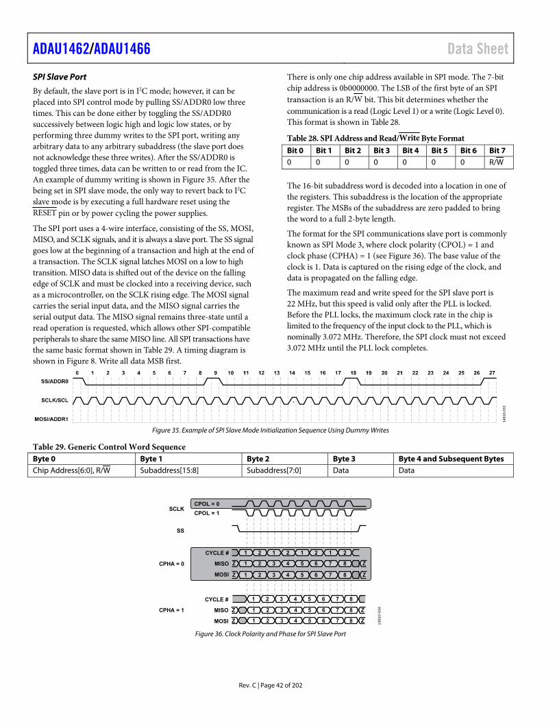
ADAU1462/ADAU1466 Data Sheet
Rev. C | Page 42 of 202
SPI Slave Port
By default, the slave port is in I2C mode; however, it can be placed into SPI control mode by pulling SS/ADDR0 low three times. This can be done either by toggling the SS/ADDR0 successively between logic high and logic low states, or by performing three dummy writes to the SPI port, writing any arbitrary data to any arbitrary subaddress (the slave port does not acknowledge these three writes). After the SS/ADDR0 is toggled three times, data can be written to or read from the IC. An example of dummy writing is shown in Figure 35. After the being set in SPI slave mode, the only way to revert back to I2C slave mode is by executing a full hardware reset using the RESET pin or by power cycling the power supplies.
The SPI port uses a 4-wire interface, consisting of the SS, MOSI, MISO, and SCLK signals, and it is always a slave port. The SS signal goes low at the beginning of a transaction and high at the end of a transaction. The SCLK signal latches MOSI on a low to high transition. MISO data is shifted out of the device on the falling edge of SCLK and must be clocked into a receiving device, such as a microcontroller, on the SCLK rising edge. The MOSI signal carries the serial input data, and the MISO signal carries the serial output data. The MISO signal remains three-state until a read operation is requested, which allows other SPI-compatible peripherals to share the same MISO line. All SPI transactions have the same basic format shown in Table 29. A timing diagram is shown in Figure 8. Write all data MSB first.
There is only one chip address available in SPI mode. The 7-bit chip address is 0b0000000. The LSB of the first byte of an SPI transaction is an R/W bit. This bit determines whether the communication is a read (Logic Level 1) or a write (Logic Level 0). This format is shown in Table 28.
Table 28. SPI Address and Read/Write Byte Format Bit 0 Bit 1 Bit 2 Bit 3 Bit 4 Bit 5 Bit 6 Bit 7 0 0 0 0 0 0 0 R/W
The 16-bit subaddress word is decoded into a location in one of the registers. This subaddress is the location of the appropriate register. The MSBs of the subaddress are zero padded to bring the word to a full 2-byte length.
The format for the SPI communications slave port is commonly known as SPI Mode 3, where clock polarity (CPOL) = 1 and clock phase (CPHA) = 1 (see Figure 36). The base value of the clock is 1. Data is captured on the rising edge of the clock, and data is propagated on the falling edge.
The maximum read and write speed for the SPI slave port is 22 MHz, but this speed is valid only after the PLL is locked. Before the PLL locks, the maximum clock rate in the chip is limited to the frequency of the input clock to the PLL, which is nominally 3.072 MHz. Therefore, the SPI clock must not exceed 3.072 MHz until the PLL lock completes.
148
10-0
33
Figure 35. Example of SPI Slave Mode Initialization Sequence Using Dummy Writes
Table 29. Generic Control Word Sequence Byte 0 Byte 1 Byte 2 Byte 3 Byte 4 and Subsequent Bytes Chip Address[6:0], R/W Subaddress[15:8] Subaddress[7:0] Data Data
CPOL = 0
CPOL = 1SCLK
SS
CPHA = 0
CPHA = 1
1 2 1 2 1 2 1 2
1 2 3 4 5 6 7 8
1 2 3 4 5 6 7 8
1
ZMISO
CYCLE #
MOSI
MISO
CYCLE #
MOSI
2 3 4 5 6 7 8
Z1 2 3 4 5 6 7 8
Z Z1 2 3 4 5 6 7 8
Z
Z
Z
Z
14
81
0-0
34
Figure 36. Clock Polarity and Phase for SPI Slave Port
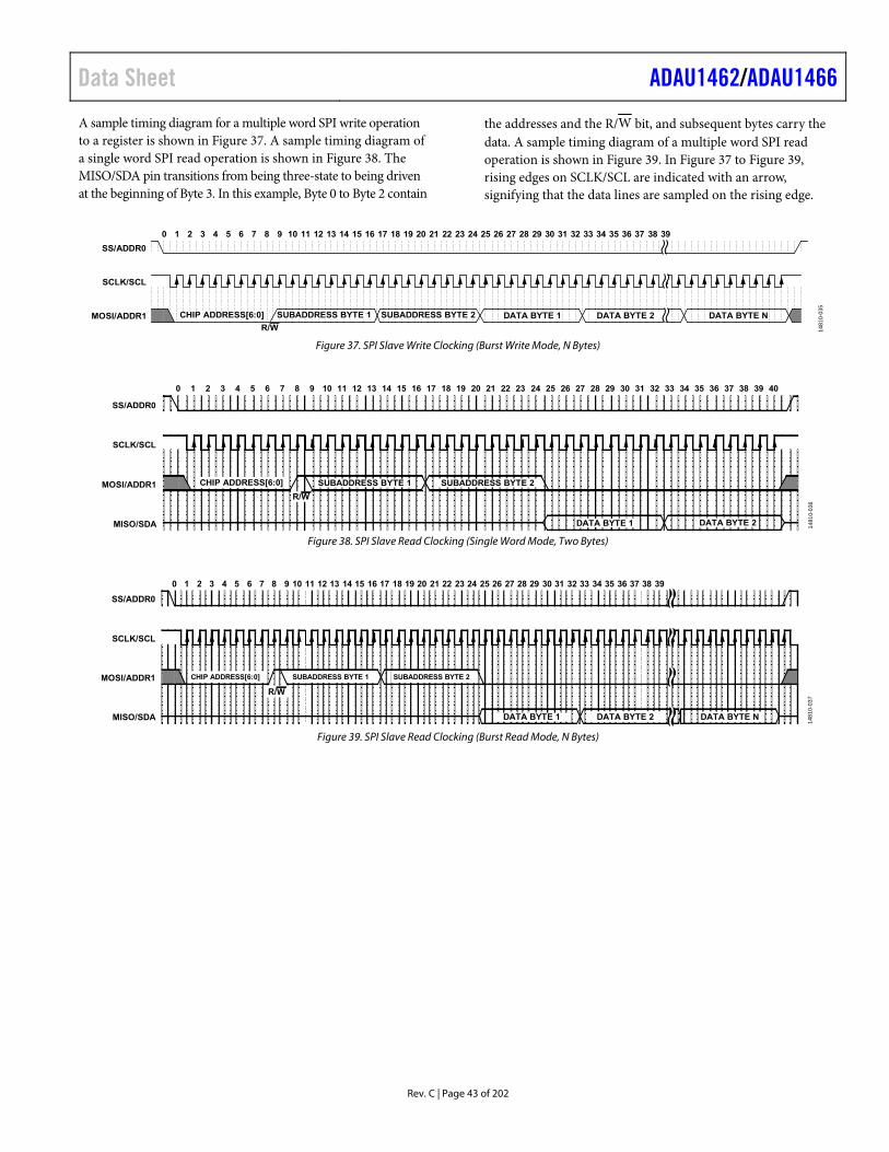
Data Sheet ADAU1462/ADAU1466
Rev. C | Page 43 of 202
A sample timing diagram for a multiple word SPI write operation to a register is shown in Figure 37. A sample timing diagram of a single word SPI read operation is shown in Figure 38. The MISO/SDA pin transitions from being three-state to being driven at the beginning of Byte 3. In this example, Byte 0 to Byte 2 contain
the addresses and the R/W bit, and subsequent bytes carry the data. A sample timing diagram of a multiple word SPI read operation is shown in Figure 39. In Figure 37 to Figure 39, rising edges on SCLK/SCL are indicated with an arrow, signifying that the data lines are sampled on the rising edge.
0 1 2 3 4 5 6 7 8 9 10 11 12 13 14 15 16 17 18 19 20 21 22 23 24 25 26 27 28 29 30 31 32 33 34 35 36 37 38 39
R/W
SS/ADDR0
SCLK/SCL
MOSI/ADDR1 CHIP ADDRESS[6:0] SUBADDRESS BYTE 1 SUBADDRESS BYTE 2 DATA BYTE 1 DATA BYTE 2 DATA BYTE N
1481
0-03
5
Figure 37. SPI Slave Write Clocking (Burst Write Mode, N Bytes)
0 1 2 3 4 5 6 7 8 9 10 11 12 13 14 15 16 17 18 19 20 21 22 23 24 25 26 27 28 29 30 31 32 33 34 35 36 37 38 39 40
SS/ADDR0
SCLK/SCL
MOSI/ADDR1
MISO/SDA DATA BYTE 1 DATA BYTE 2
CHIP ADDRESS[6:0] SUBADDRESS BYTE 1 SUBADDRESS BYTE 2
R/W
1481
0-03
6
Figure 38. SPI Slave Read Clocking (Single Word Mode, Two Bytes)
0 1 2 3 4 5 6 7 8 9 10 11 12 13 14 15 16 17 18 19 20 21 22 23 24 25 26 27 28 29 30 31 32 33 34 35 36 37 38 39
SS/ADDR0
SCLK/SCL
MOSI/ADDR1
MISO/SDA DATA BYTE 1 DATA BYTE 2 DATA BYTE N
CHIP ADDRESS[6:0] SUBADDRESS BYTE 2SUBADDRESS BYTE 1
R/W
1481
0-03
7
Figure 39. SPI Slave Read Clocking (Burst Read Mode, N Bytes)
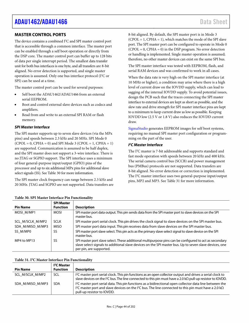
ADAU1462/ADAU1466 Data Sheet
Rev. C | Page 44 of 202
MASTER CONTROL PORTS The device contains a combined I2C and SPI master control port that is accessible through a common interface. The master port can be enabled through a self boot operation or directly from the DSP core. The master control port can buffer up to 128 bits of data per single interrupt period. The smallest data transfer unit for both bus interfaces is one byte, and all transfers are 8-bit aligned. No error detection is supported, and single master operation is assumed. Only one bus interface protocol (I2C or SPI) can be used at a time.
The master control port can be used for several purposes:
Self boot the ADAU1462/ADAU1466 from an external serial EEPROM.
Boot and control external slave devices such as codecs and amplifiers.
Read from and write to an external SPI RAM or flash memory.
SPI Master Interface
The SPI master supports up to seven slave devices (via the MPx pins) and speeds between 2.3 kHz and 20 MHz. SPI Mode 0 (CPOL = 0, CPHA = 0) and SPI Mode 3 (CPOL = 1, CPHA = 1) are supported. Communication is assumed to be half duplex, and the SPI master does not support a 3-wire interface. There is no JTAG or SGPIO support. The SPI interface uses a minimum of four general-purpose input/output (GPIO) pins of the processor and up to six additional MPx pins for additional slave select signals (SS). See Table 30 for more information.
The SPI master clock frequency can range between 2.3 kHz and 20 MHz. JTAG and SGPIO are not supported. Data transfers are
8-bit aligned. By default, the SPI master port is in Mode 3 (CPOL = 1, CPHA = 1), which matches the mode of the SPI slave port. The SPI master port can be configured to operate in Mode 0 (CPOL = 0, CPHA = 0) in the DSP program. No error detection or handling is implemented. Single master operation is assumed; therefore, no other master devices can exist on the same SPI bus.
The SPI master interface was tested with EEPROM, flash, and serial RAM devices and was confirmed to work in all cases.
When the data rate is very high on the SPI master interface (at 10 MHz or higher), a condition may arise where there is a high level of current draw on the IOVDD supply, which can lead to sagging of the internal IOVDD supply. To avoid potential issues, design the PCB such that the traces connecting the SPI master interface to external devices are kept as short as possible, and the slew rate and drive strength for SPI master interface pins are kept to a minimum to keep current draw as low as possible. Keeping IOVDD low (2.5 V or 1.8 V) also reduces the IOVDD current draw.
SigmaStudio generates EEPROM images for self boot systems, requiring no manual SPI master port configuration or program-ming on the part of the user.
I2C Master Interface
The I2C master is 7-bit addressable and supports standard and fast mode operation with speeds between 20 kHz and 400 kHz. The serial camera control bus (SCCB) and power management bus (PMBus) protocols are not supported. Data transfers are 8-bit aligned. No error detection or correction is implemented. The I2C master interface uses two general-purpose input/output pins, MP2 and MP3. See Table 31 for more information.
Table 30. SPI Master Interface Pin Functionality
Pin Name SPI Master Function Description
MOSI_M/MP1 MOSI SPI master port data output. This pin sends data from the SPI master port to slave devices on the SPI master bus.
SCL_M/SCLK_M/MP2 SCLK SPI master port serial clock. This pin drives the clock signal to slave devices on the SPI master bus. SDA_M/MISO_M/MP3 MISO SPI master port data input. This pin receives data from slave devices on the SPI master bus. SS_M/MP0 SS SPI master port slave select. This pin acts as the primary slave select signal to slave device on the SPI
master bus. MP4 to MP13 SS SPI master port slave select. These additional multipurpose pins can be configured to act as secondary
slave select signals to additional slave devices on the SPI master bus. Up to seven slave devices, one per pin, are supported.
Table 31. I2C Master Interface Pin Functionality
Pin Name I2C Master Function Description
SCL_M/SCLK_M/MP2 SCL I2C master port serial clock. This pin functions as an open collector output and drives a serial clock to slave devices on the I2C bus. The line connected to this pin must have a 2.0 kΩ pull-up resistor to IOVDD.
SDA_M/MISO_M/MP3 SDA I2C master port serial data. This pin functions as a bidirectional open collector data line between the I2C master port and slave devices on the I2C bus. The line connected to this pin must have a 2.0 kΩ pull-up resistor to IOVDD.
Data Sheet ADAU1462/ADAU1466
Rev. C | Page 45 of 202
SELF BOOT The master control port is capable of booting the device from a single EEPROM by connecting the SELFBOOT pin to logic high (IOVDD) and powering up the power supplies while the RESET pin is pulled high. This initiates a self boot operation, in which the master control port downloads all required memory and register settings and automatically starts executing the DSP program without requiring external intervention or supervision. A self boot operation can also be triggered while the device is already in operation by initiating a rising edge of the RESET pin while the SELFBOOT pin is held high. When the self boot operation begins, the state of the SS_M/MP0 pin determines whether the SPI master or the I2C master carries out the self boot operation. If the SS_M/MP0 pin is connected to logic low, the I2C master port carries out the self boot operation. Otherwise, connect this pin to the slave select pin of the external slave device. The SPI master port then carries out the self boot operation.
When self booting from SPI, the chip assumes the following:
The slave EEPROM is selected via the SS_M/MP0 pin. The slave EEPROM has 16-bit or 24-bit addressing, giving
it a total memory size of between 4 kb and 64 Mb. The slave EEPROM supports serial clock frequencies down
to 1 MHz or lower (a majority of the self boot operation uses a much higher clock frequency, but the initial transactions are performed at a slower frequency).
The data stored in the slave EEPROM follows the format described in the EEPROM Self Boot Data Format section.
The data is stored in the slave EEPROM with the MSB first. The slave EEPROM supports SPI Mode 3. The slave EEPROM sequential read operation has the
command of 0x03. The slave EEPROM can be accessed immediately after it is
powered up, with no manual configuration required.
When self booting from I2C, the chip assumes the following:
The slave EEPROM has I2C Address 0x50. The slave EEPROM has 16-bit addressing, giving it a size of
between 16 kb and 512 kb. The slave EEPROM supports standard mode clock
frequencies of 100 kHz and lower (a majority of the self boot operation uses a much higher clock frequency, but the initial transactions are performed at a slower frequency).
The data stored in the slave EEPROM follows the format described in the EEPROM Self Boot Data Format section.
The slave EEPROM can be accessed immediately after it is powered, with no manual configuration required.
Self Boot Failure
The SPI or I2C master port attempts to self boot from the EEPROM three times. If all three self boot attempts fail, the SigmaDSP core issues a software panic and then enters a sleep state. During a self boot operation, the panic manager is unable to output a panic flag on a multipurpose pin. Therefore, the only way to debug a self boot failure is by reading back the status of Register 0xF427 (PANIC_FLAG) and Register 0xF428 (PANIC_CODE). The contents of Register 0xF428 indicate the nature of the failure.
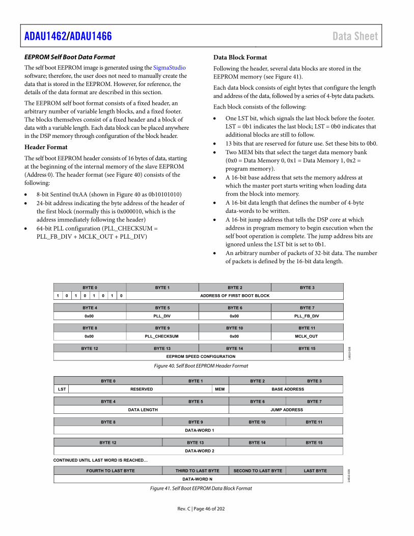
ADAU1462/ADAU1466 Data Sheet
Rev. C | Page 46 of 202
EEPROM Self Boot Data Format
The self boot EEPROM image is generated using the SigmaStudio software; therefore, the user does not need to manually create the data that is stored in the EEPROM. However, for reference, the details of the data format are described in this section.
The EEPROM self boot format consists of a fixed header, an arbitrary number of variable length blocks, and a fixed footer. The blocks themselves consist of a fixed header and a block of data with a variable length. Each data block can be placed anywhere in the DSP memory through configuration of the block header.
Header Format
The self boot EEPROM header consists of 16 bytes of data, starting at the beginning of the internal memory of the slave EEPROM (Address 0). The header format (see Figure 40) consists of the following:
8-bit Sentinel 0xAA (shown in Figure 40 as 0b10101010) 24-bit address indicating the byte address of the header of
the first block (normally this is 0x000010, which is the address immediately following the header)
64-bit PLL configuration (PLL_CHECKSUM = PLL_FB_DIV + MCLK_OUT + PLL_DIV)
Data Block Format
Following the header, several data blocks are stored in the EEPROM memory (see Figure 41).
Each data block consists of eight bytes that configure the length and address of the data, followed by a series of 4-byte data packets.
Each block consists of the following:
One LST bit, which signals the last block before the footer. LST = 0b1 indicates the last block; LST = 0b0 indicates that additional blocks are still to follow.
13 bits that are reserved for future use. Set these bits to 0b0. Two MEM bits that select the target data memory bank
(0x0 = Data Memory 0, 0x1 = Data Memory 1, 0x2 = program memory).
A 16-bit base address that sets the memory address at which the master port starts writing when loading data from the block into memory.
A 16-bit data length that defines the number of 4-byte data-words to be written.
A 16-bit jump address that tells the DSP core at which address in program memory to begin execution when the self boot operation is complete. The jump address bits are ignored unless the LST bit is set to 0b1.
An arbitrary number of packets of 32-bit data. The number of packets is defined by the 16-bit data length.
BYTE 0 BYTE 1 BYTE 2 BYTE 3
1 0 1 0 1 0 1 0 ADDRESS OF FIRST BOOT BLOCK
BYTE 4 BYTE 5 BYTE 6 BYTE 7
0x00 PLL_DIV 0x00 PLL_FB_DIV
BYTE 8 BYTE 9 BYTE 10 BYTE 11
0x00 PLL_CHECKSUM 0x00 MCLK_OUT
BYTE 12 BYTE 13 BYTE 14 BYTE 15
EEPROM SPEED CONFIGURATION
1481
0-03
8
Figure 40. Self Boot EEPROM Header Format
BYTE 0 BYTE 1 BYTE 2 BYTE 3
LST RESERVED MEM BASE ADDRESS
BYTE 4 BYTE 5 BYTE 6 BYTE 7
DATA LENGTH JUMP ADDRESS
BYTE 8 BYTE 9 BYTE 10 BYTE 11
DATA-WORD 1
BYTE 12 BYTE 13 BYTE 14 BYTE 15
DATA-WORD 2
FOURTH TO LAST BYTE THIRD TO LAST BYTE SECOND TO LAST BYTE LAST BYTE
DATA-WORD N
CONTINUED UNTIL LAST WORD IS REACHED…
148
10-0
39
Figure 41. Self Boot EEPROM Data Block Format
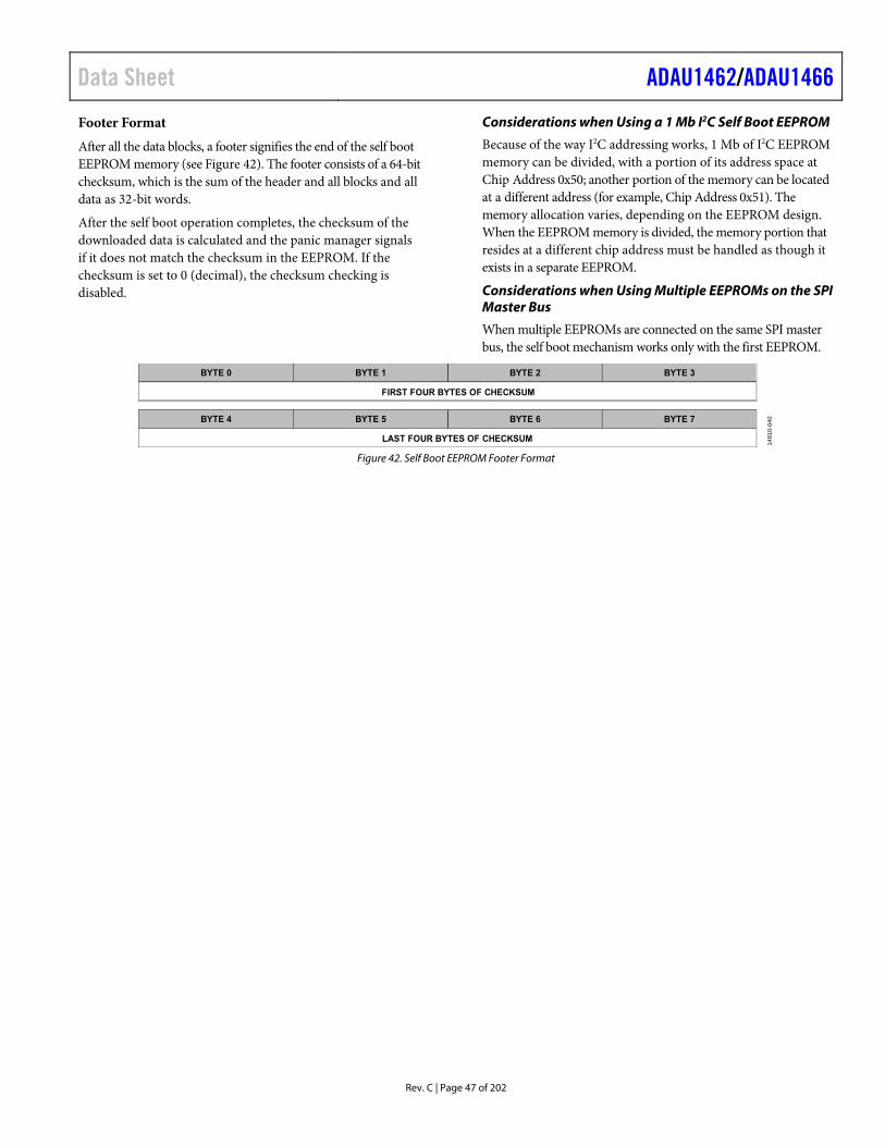
Data Sheet ADAU1462/ADAU1466
Rev. C | Page 47 of 202
Footer Format
After all the data blocks, a footer signifies the end of the self boot EEPROM memory (see Figure 42). The footer consists of a 64-bit checksum, which is the sum of the header and all blocks and all data as 32-bit words.
After the self boot operation completes, the checksum of the downloaded data is calculated and the panic manager signals if it does not match the checksum in the EEPROM. If the checksum is set to 0 (decimal), the checksum checking is disabled.
Considerations when Using a 1 Mb I2C Self Boot EEPROM
Because of the way I2C addressing works, 1 Mb of I2C EEPROM memory can be divided, with a portion of its address space at Chip Address 0x50; another portion of the memory can be located at a different address (for example, Chip Address 0x51). The memory allocation varies, depending on the EEPROM design. When the EEPROM memory is divided, the memory portion that resides at a different chip address must be handled as though it exists in a separate EEPROM.
Considerations when Using Multiple EEPROMs on the SPI Master Bus
When multiple EEPROMs are connected on the same SPI master bus, the self boot mechanism works only with the first EEPROM.
BYTE 0 BYTE 1 BYTE 2 BYTE 3
FIRST FOUR BYTES OF CHECKSUM
BYTE 4 BYTE 5 BYTE 6 BYTE 7
LAST FOUR BYTES OF CHECKSUM
14
810
-040
Figure 42. Self Boot EEPROM Footer Format
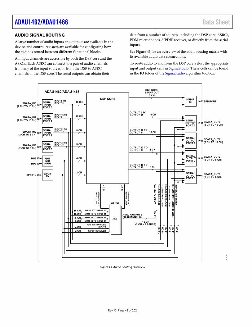
ADAU1462/ADAU1466 Data Sheet
Rev. C | Page 48 of 202
AUDIO SIGNAL ROUTING A large number of audio inputs and outputs are available in the device, and control registers are available for configuring how the audio is routed between different functional blocks.
All input channels are accessible by both the DSP core and the ASRCs. Each ASRC can connect to a pair of audio channels from any of the input sources or from the DSP to ASRC channels of the DSP core. The serial outputs can obtain their
data from a number of sources, including the DSP core, ASRCs, PDM microphones, S/PDIF receiver, or directly from the serial inputs.
See Figure 43 for an overview of the audio routing matrix with its available audio data connections.
To route audio to and from the DSP core, select the appropriate input and output cells in SigmaStudio. These cells can be found in the IO folder of the SigmaStudio algorithm toolbox.
INPUT 0 TOINPUT 15SDATA_IN0
(2 CH TO 16 CH)
SDATA_IN1(2 CH TO 16 CH)
SDATA_IN2(2 CH TO 8 CH)
SDATA_IN3(2 CH TO 8 CH)
SDATA_OUT0(2 CH TO 16 CH)
SDATA_OUT1(2 CH TO 16 CH)
SDATA_OUT2(2 CH TO 8 CH)
SDATA_OUT3(2 CH TO 8 CH)
SPDIFIN S/PDIFRx
DSP CORE
ASRCs
(×8)
SPDIFOUT
MP6
MP7
INPUT 16 TOINPUT 31
INPUT 32 TOINPUT 39
INPUT 40 TOINPUT 47
AS
RC
OU
TP
UT
S
INPUT 0 TO INPUT 15
INPUT 16 TO INPUT 31
INPUT 32 TO INPUT 39
INPUT 40 TO INPUT 47
PDM MICROPHONEINPUTS
S/PDIF RECEIVER
ASRC OUTPUTS(16 CHANNELS)
OUTPUT 0 TOOUTPUT 15
OUTPUT 16 TOOUTPUT 31
OUTPUT 32 TOOUTPUT 39
OUTPUT 40 TOOUTPUT 47
SERIALS/PDIF
Tx
SERIALOUTPUTPORT 1
SERIALOUTPUTPORT 2
SERIALOUTPUTPORT 3
SERIALOUTPUTPORT 0
16 C
H
16 CH(2 CH × 8 ASRCS)
16 C
H
16 C
H
16 C
H
16 CH
16 CH
8 CH
8 CH
16 C
H
8 C
H
8 C
H
4 C
H
2 C
H
16 CH
16 CH
8 CH
8 CH
4 CH
2 CH
16 CH
16 CH
8 CH
8 CH
4 CH
2 CH
INP
UT
0 T
O I
NP
UT
15
INP
UT
16
TO
IN
PU
T 3
1
INP
UT
32
TO
IN
PU
T 3
9
INP
UT
40
TO
IN
PU
T 4
7
PD
M M
ICR
OP
HO
NE
IN
PU
TS
S/P
DIF
RE
CE
IVE
R
DS
P T
O A
SR
C(1
6 C
HA
NN
EL
S)
AS
RC
TO
DS
P(1
6 C
HA
NN
EL
S)
DSP CORES/PDIF OUT
2 CH
INPUTPORT 0
SERIALINPUT
PORT 1
SERIALINPUT
PORT 2
SERIALINPUT
PORT 3
PDMMIC
INPUT
ADAU1462/ADAU1466
148
10-0
41
Figure 43. Audio Routing Overview
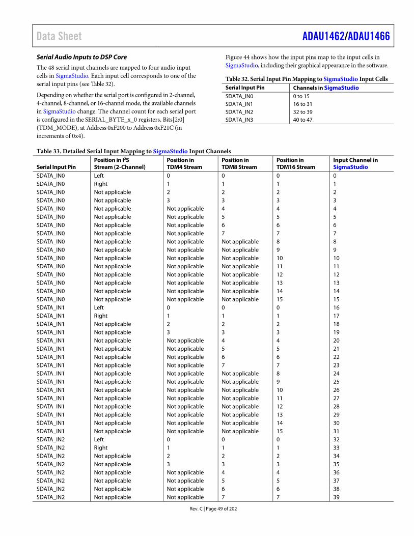
Data Sheet ADAU1462/ADAU1466
Rev. C | Page 49 of 202
Serial Audio Inputs to DSP Core
The 48 serial input channels are mapped to four audio input cells in SigmaStudio. Each input cell corresponds to one of the serial input pins (see Table 32).
Depending on whether the serial port is configured in 2-channel, 4-channel, 8-channel, or 16-channel mode, the available channels in SigmaStudio change. The channel count for each serial port is configured in the SERIAL_BYTE_x_0 registers, Bits[2:0] (TDM_MODE), at Address 0xF200 to Address 0xF21C (in increments of 0x4).
Figure 44 shows how the input pins map to the input cells in SigmaStudio, including their graphical appearance in the software.
Table 32. Serial Input Pin Mapping to SigmaStudio Input Cells Serial Input Pin Channels in SigmaStudio
SDATA_IN0 0 to 15 SDATA_IN1 16 to 31 SDATA_IN2 32 to 39 SDATA_IN3 40 to 47
Table 33. Detailed Serial Input Mapping to SigmaStudio Input Channels
Serial Input Pin Position in I2S Stream (2-Channel)
Position in TDM4 Stream
Position in TDM8 Stream
Position in TDM16 Stream
Input Channel in SigmaStudio
SDATA_IN0 Left 0 0 0 0 SDATA_IN0 Right 1 1 1 1 SDATA_IN0 Not applicable 2 2 2 2 SDATA_IN0 Not applicable 3 3 3 3 SDATA_IN0 Not applicable Not applicable 4 4 4 SDATA_IN0 Not applicable Not applicable 5 5 5 SDATA_IN0 Not applicable Not applicable 6 6 6 SDATA_IN0 Not applicable Not applicable 7 7 7 SDATA_IN0 Not applicable Not applicable Not applicable 8 8 SDATA_IN0 Not applicable Not applicable Not applicable 9 9 SDATA_IN0 Not applicable Not applicable Not applicable 10 10 SDATA_IN0 Not applicable Not applicable Not applicable 11 11 SDATA_IN0 Not applicable Not applicable Not applicable 12 12 SDATA_IN0 Not applicable Not applicable Not applicable 13 13 SDATA_IN0 Not applicable Not applicable Not applicable 14 14 SDATA_IN0 Not applicable Not applicable Not applicable 15 15 SDATA_IN1 Left 0 0 0 16 SDATA_IN1 Right 1 1 1 17 SDATA_IN1 Not applicable 2 2 2 18 SDATA_IN1 Not applicable 3 3 3 19 SDATA_IN1 Not applicable Not applicable 4 4 20 SDATA_IN1 Not applicable Not applicable 5 5 21 SDATA_IN1 Not applicable Not applicable 6 6 22 SDATA_IN1 Not applicable Not applicable 7 7 23 SDATA_IN1 Not applicable Not applicable Not applicable 8 24 SDATA_IN1 Not applicable Not applicable Not applicable 9 25 SDATA_IN1 Not applicable Not applicable Not applicable 10 26 SDATA_IN1 Not applicable Not applicable Not applicable 11 27 SDATA_IN1 Not applicable Not applicable Not applicable 12 28 SDATA_IN1 Not applicable Not applicable Not applicable 13 29 SDATA_IN1 Not applicable Not applicable Not applicable 14 30 SDATA_IN1 Not applicable Not applicable Not applicable 15 31 SDATA_IN2 Left 0 0 0 32 SDATA_IN2 Right 1 1 1 33 SDATA_IN2 Not applicable 2 2 2 34 SDATA_IN2 Not applicable 3 3 3 35 SDATA_IN2 Not applicable Not applicable 4 4 36 SDATA_IN2 Not applicable Not applicable 5 5 37 SDATA_IN2 Not applicable Not applicable 6 6 38 SDATA_IN2 Not applicable Not applicable 7 7 39
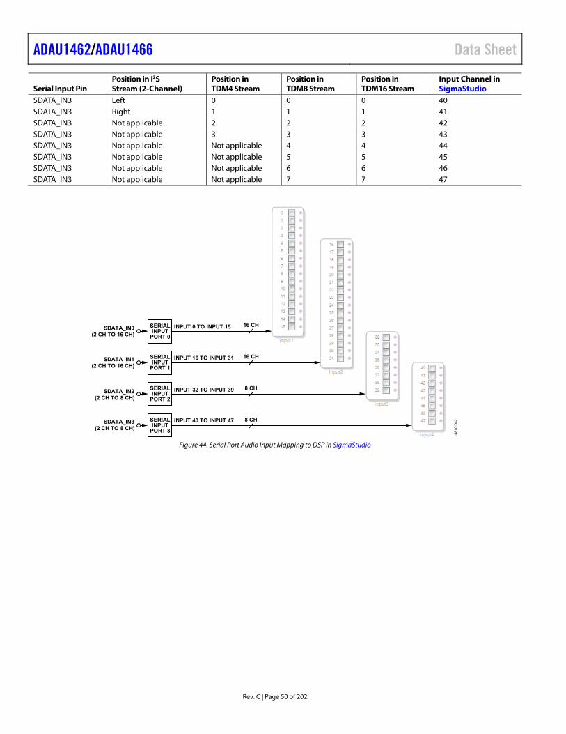
ADAU1462/ADAU1466 Data Sheet
Rev. C | Page 50 of 202
Serial Input Pin Position in I2S Stream (2-Channel)
Position in TDM4 Stream
Position in TDM8 Stream
Position in TDM16 Stream
Input Channel in SigmaStudio
SDATA_IN3 Left 0 0 0 40 SDATA_IN3 Right 1 1 1 41 SDATA_IN3 Not applicable 2 2 2 42 SDATA_IN3 Not applicable 3 3 3 43 SDATA_IN3 Not applicable Not applicable 4 4 44 SDATA_IN3 Not applicable Not applicable 5 5 45 SDATA_IN3 Not applicable Not applicable 6 6 46 SDATA_IN3 Not applicable Not applicable 7 7 47
INPUT 0 TO INPUT 15SDATA_IN0(2 CH TO 16 CH)
SDATA_IN1(2 CH TO 16 CH)
SDATA_IN2(2 CH TO 8 CH)
SDATA_IN3(2 CH TO 8 CH)
INPUT 16 TO INPUT 31
INPUT 32 TO INPUT 39
INPUT 40 TO INPUT 47
SERIALINPUT
PORT 0
SERIALINPUT
PORT 1
SERIALINPUT
PORT 2
SERIALINPUT
PORT 3
16 CH
16 CH
8 CH
8 CH
148
10-0
42
Figure 44. Serial Port Audio Input Mapping to DSP in SigmaStudio
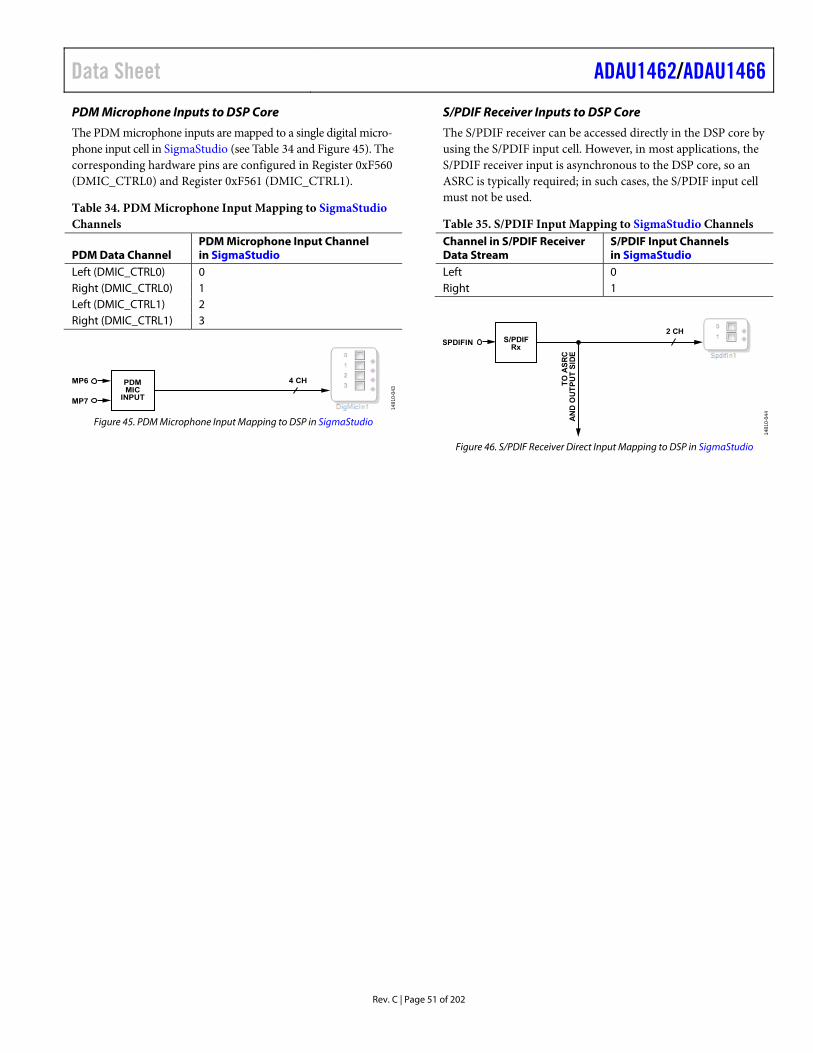
Data Sheet ADAU1462/ADAU1466
Rev. C | Page 51 of 202
PDM Microphone Inputs to DSP Core
The PDM microphone inputs are mapped to a single digital micro-phone input cell in SigmaStudio (see Table 34 and Figure 45). The corresponding hardware pins are configured in Register 0xF560 (DMIC_CTRL0) and Register 0xF561 (DMIC_CTRL1).
Table 34. PDM Microphone Input Mapping to SigmaStudio Channels
PDM Data Channel PDM Microphone Input Channel in SigmaStudio
Left (DMIC_CTRL0) 0 Right (DMIC_CTRL0) 1 Left (DMIC_CTRL1) 2 Right (DMIC_CTRL1) 3
MP6
MP7
PDMMIC
INPUT
4 CH
1481
0-04
3
Figure 45. PDM Microphone Input Mapping to DSP in SigmaStudio
S/PDIF Receiver Inputs to DSP Core
The S/PDIF receiver can be accessed directly in the DSP core by using the S/PDIF input cell. However, in most applications, the S/PDIF receiver input is asynchronous to the DSP core, so an ASRC is typically required; in such cases, the S/PDIF input cell must not be used.
Table 35. S/PDIF Input Mapping to SigmaStudio Channels Channel in S/PDIF Receiver Data Stream
S/PDIF Input Channels in SigmaStudio
Left 0 Right 1
2 CH
SPDIFIN S/PDIFRx
TO
AS
RC
AN
D O
UT
PU
T S
IDE
1481
0-04
4
Figure 46. S/PDIF Receiver Direct Input Mapping to DSP in SigmaStudio
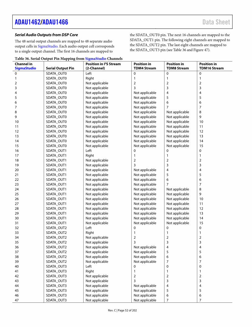
ADAU1462/ADAU1466 Data Sheet
Rev. C | Page 52 of 202
Serial Audio Outputs from DSP Core
The 48 serial output channels are mapped to 48 separate audio output cells in SigmaStudio. Each audio output cell corresponds to a single output channel. The first 16 channels are mapped to
the SDATA_OUT0 pin. The next 16 channels are mapped to the SDATA_OUT1 pin. The following eight channels are mapped to the SDATA_OUT2 pin. The last eight channels are mapped to the SDATA_OUT3 pin (see Table 36 and Figure 47).
Table 36. Serial Output Pin Mapping from SigmaStudio Channels Channel in SigmaStudio Serial Output Pin
Position in I2S Stream (2-Channel)
Position in TDM4 Stream
Position in TDM8 Stream
Position in TDM16 Stream
0 SDATA_OUT0 Left 0 0 0 1 SDATA_OUT0 Right 1 1 1 2 SDATA_OUT0 Not applicable 2 2 2 3 SDATA_OUT0 Not applicable 3 3 3 4 SDATA_OUT0 Not applicable Not applicable 4 4 5 SDATA_OUT0 Not applicable Not applicable 5 5 6 SDATA_OUT0 Not applicable Not applicable 6 6 7 SDATA_OUT0 Not applicable Not applicable 7 7 8 SDATA_OUT0 Not applicable Not applicable Not applicable 8 9 SDATA_OUT0 Not applicable Not applicable Not applicable 9 10 SDATA_OUT0 Not applicable Not applicable Not applicable 10 11 SDATA_OUT0 Not applicable Not applicable Not applicable 11 12 SDATA_OUT0 Not applicable Not applicable Not applicable 12 13 SDATA_OUT0 Not applicable Not applicable Not applicable 13 14 SDATA_OUT0 Not applicable Not applicable Not applicable 14 15 SDATA_OUT0 Not applicable Not applicable Not applicable 15 16 SDATA_OUT1 Left 0 0 0 17 SDATA_OUT1 Right 1 1 1 18 SDATA_OUT1 Not applicable 2 2 2 19 SDATA_OUT1 Not applicable 3 3 3 20 SDATA_OUT1 Not applicable Not applicable 4 4 21 SDATA_OUT1 Not applicable Not applicable 5 5 22 SDATA_OUT1 Not applicable Not applicable 6 6 23 SDATA_OUT1 Not applicable Not applicable 7 7 24 SDATA_OUT1 Not applicable Not applicable Not applicable 8 25 SDATA_OUT1 Not applicable Not applicable Not applicable 9 26 SDATA_OUT1 Not applicable Not applicable Not applicable 10 27 SDATA_OUT1 Not applicable Not applicable Not applicable 11 28 SDATA_OUT1 Not applicable Not applicable Not applicable 12 29 SDATA_OUT1 Not applicable Not applicable Not applicable 13 30 SDATA_OUT1 Not applicable Not applicable Not applicable 14 31 SDATA_OUT1 Not applicable Not applicable Not applicable 15 32 SDATA_OUT2 Left 0 0 0 33 SDATA_OUT2 Right 1 1 1 34 SDATA_OUT2 Not applicable 2 2 2 35 SDATA_OUT2 Not applicable 3 3 3 36 SDATA_OUT2 Not applicable Not applicable 4 4 37 SDATA_OUT2 Not applicable Not applicable 5 5 38 SDATA_OUT2 Not applicable Not applicable 6 6 39 SDATA_OUT2 Not applicable Not applicable 7 7 40 SDATA_OUT3 Left 0 0 0 41 SDATA_OUT3 Right 1 1 1 42 SDATA_OUT3 Not applicable 2 2 2 43 SDATA_OUT3 Not applicable 3 3 3 44 SDATA_OUT3 Not applicable Not applicable 4 4 45 SDATA_OUT3 Not applicable Not applicable 5 5 46 SDATA_OUT3 Not applicable Not applicable 6 6 47 SDATA_OUT3 Not applicable Not applicable 7 7
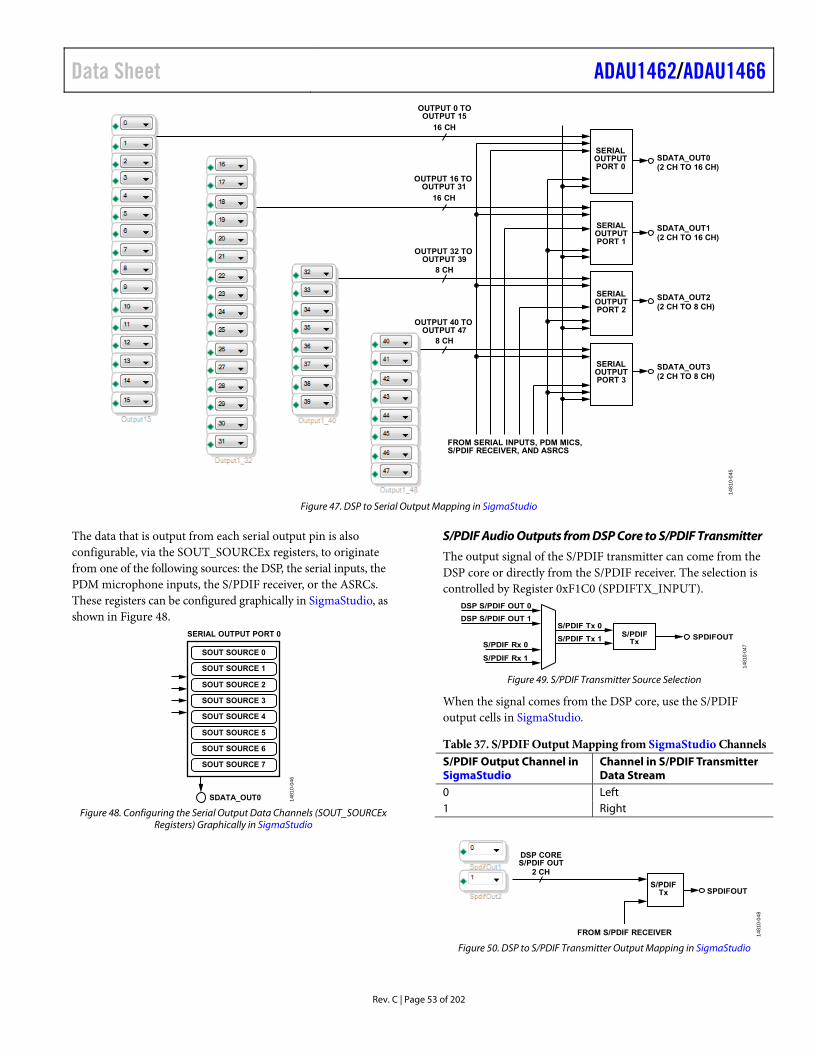
Data Sheet ADAU1462/ADAU1466
Rev. C | Page 53 of 202
OUTPUT 0 TOOUTPUT 15
16 CH
OUTPUT 16 TOOUTPUT 31
16 CH
OUTPUT 32 TOOUTPUT 39
OUTPUT 40 TOOUTPUT 47
8 CH
8 CH
FROM SERIAL INPUTS, PDM MICS,S/PDIF RECEIVER, AND ASRCS
SDATA_OUT0(2 CH TO 16 CH)
SDATA_OUT1(2 CH TO 16 CH)
SDATA_OUT2(2 CH TO 8 CH)
SDATA_OUT3(2 CH TO 8 CH)
SERIALOUTPUTPORT 1
SERIALOUTPUTPORT 2
SERIALOUTPUTPORT 3
SERIALOUTPUTPORT 0
148
10-0
45
Figure 47. DSP to Serial Output Mapping in SigmaStudio
The data that is output from each serial output pin is also configurable, via the SOUT_SOURCEx registers, to originate from one of the following sources: the DSP, the serial inputs, the PDM microphone inputs, the S/PDIF receiver, or the ASRCs. These registers can be configured graphically in SigmaStudio, as shown in Figure 48.
SOUT SOURCE 0
SOUT SOURCE 1
SOUT SOURCE 2
SOUT SOURCE 3
SOUT SOURCE 4
SOUT SOURCE 5
SOUT SOURCE 6
SOUT SOURCE 7
SDATA_OUT0
SERIAL OUTPUT PORT 0
14
810-
046
Figure 48. Configuring the Serial Output Data Channels (SOUT_SOURCEx
Registers) Graphically in SigmaStudio
S/PDIF Audio Outputs from DSP Core to S/PDIF Transmitter
The output signal of the S/PDIF transmitter can come from the DSP core or directly from the S/PDIF receiver. The selection is controlled by Register 0xF1C0 (SPDIFTX_INPUT).
S/PDIF Rx 0
S/PDIF Rx 1
S/PDIF Tx 0
S/PDIF Tx 1
DSP S/PDIF OUT 0
DSP S/PDIF OUT 1
SPDIFOUTS/PDIFTx
1481
0-04
7
Figure 49. S/PDIF Transmitter Source Selection
When the signal comes from the DSP core, use the S/PDIF output cells in SigmaStudio.
Table 37. S/PDIF Output Mapping from SigmaStudio Channels S/PDIF Output Channel in SigmaStudio
Channel in S/PDIF Transmitter Data Stream
0 Left 1 Right
SPDIFOUTS/PDIF
Tx
DSP CORES/PDIF OUT
2 CH
FROM S/PDIF RECEIVER 1481
0-04
8
Figure 50. DSP to S/PDIF Transmitter Output Mapping in SigmaStudio
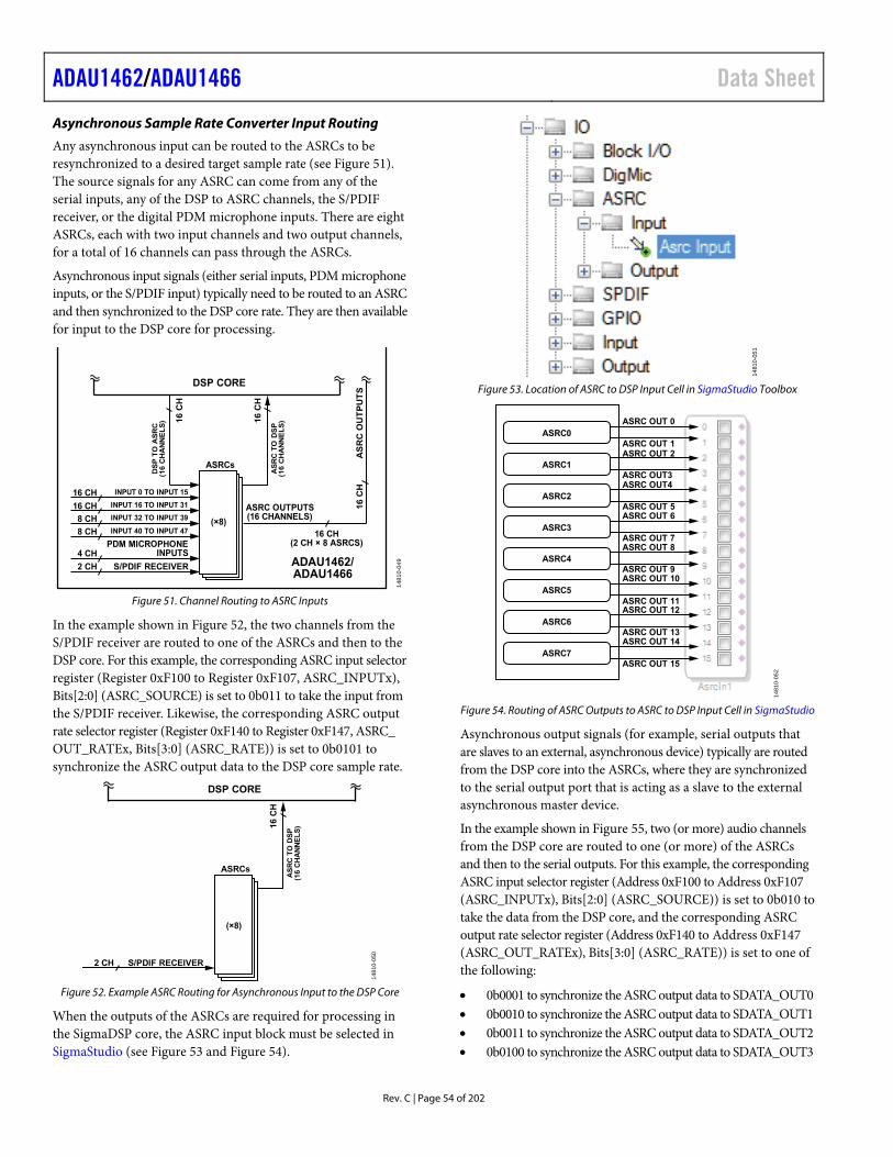
ADAU1462/ADAU1466 Data Sheet
Rev. C | Page 54 of 202
Asynchronous Sample Rate Converter Input Routing
Any asynchronous input can be routed to the ASRCs to be resynchronized to a desired target sample rate (see Figure 51). The source signals for any ASRC can come from any of the serial inputs, any of the DSP to ASRC channels, the S/PDIF receiver, or the digital PDM microphone inputs. There are eight ASRCs, each with two input channels and two output channels, for a total of 16 channels can pass through the ASRCs.
Asynchronous input signals (either serial inputs, PDM microphone inputs, or the S/PDIF input) typically need to be routed to an ASRC and then synchronized to the DSP core rate. They are then available for input to the DSP core for processing.
ASRCs
(×8)
INPUT 0 TO INPUT 15
INPUT 16 TO INPUT 31
INPUT 32 TO INPUT 39
INPUT 40 TO INPUT 47
PDM MICROPHONEINPUTS
S/PDIF RECEIVER
ASRC OUTPUTS(16 CHANNELS)
16 CH(2 CH × 8 ASRCS)
16 C
H
16 C
H
16 CH
16 CH
8 CH
8 CH
4 CH
2 CH
DS
P T
O A
SR
C(1
6 C
HA
NN
EL
S)
AS
RC
TO
DS
P(1
6 C
HA
NN
EL
S)
DSP CORE
AS
RC
OU
TP
UT
S16 C
H
ADAU1462/ADAU1466
148
10-0
49
Figure 51. Channel Routing to ASRC Inputs
In the example shown in Figure 52, the two channels from the S/PDIF receiver are routed to one of the ASRCs and then to the DSP core. For this example, the corresponding ASRC input selector register (Register 0xF100 to Register 0xF107, ASRC_INPUTx), Bits[2:0] (ASRC_SOURCE) is set to 0b011 to take the input from the S/PDIF receiver. Likewise, the corresponding ASRC output rate selector register (Register 0xF140 to Register 0xF147, ASRC_ OUT_RATEx, Bits[3:0] (ASRC_RATE)) is set to 0b0101 to synchronize the ASRC output data to the DSP core sample rate.
ASRCs
(×8)
S/PDIF RECEIVER
16 C
H
2 CH
AS
RC
TO
DS
P(1
6 C
HA
NN
EL
S)
DSP CORE
1481
0-0
50
Figure 52. Example ASRC Routing for Asynchronous Input to the DSP Core
When the outputs of the ASRCs are required for processing in the SigmaDSP core, the ASRC input block must be selected in SigmaStudio (see Figure 53 and Figure 54).
1481
0-05
1
Figure 53. Location of ASRC to DSP Input Cell in SigmaStudio Toolbox
ASRC0ASRC OUT 0
ASRC1
ASRC2
ASRC3
ASRC4
ASRC5
ASRC6
ASRC7
ASRC OUT 1ASRC OUT 2
ASRC OUT3ASRC OUT4
ASRC OUT 5ASRC OUT 6
ASRC OUT 7ASRC OUT 8
ASRC OUT 9ASRC OUT 10
ASRC OUT 11ASRC OUT 12
ASRC OUT 13ASRC OUT 14
ASRC OUT 15
14
81
0-0
52
Figure 54. Routing of ASRC Outputs to ASRC to DSP Input Cell in SigmaStudio
Asynchronous output signals (for example, serial outputs that are slaves to an external, asynchronous device) typically are routed from the DSP core into the ASRCs, where they are synchronized to the serial output port that is acting as a slave to the external asynchronous master device.
In the example shown in Figure 55, two (or more) audio channels from the DSP core are routed to one (or more) of the ASRCs and then to the serial outputs. For this example, the corresponding ASRC input selector register (Address 0xF100 to Address 0xF107 (ASRC_INPUTx), Bits[2:0] (ASRC_SOURCE)) is set to 0b010 to take the data from the DSP core, and the corresponding ASRC output rate selector register (Address 0xF140 to Address 0xF147 (ASRC_OUT_RATEx), Bits[3:0] (ASRC_RATE)) is set to one of the following:
0b0001 to synchronize the ASRC output data to SDATA_OUT0 0b0010 to synchronize the ASRC output data to SDATA_OUT1 0b0011 to synchronize the ASRC output data to SDATA_OUT2 0b0100 to synchronize the ASRC output data to SDATA_OUT3
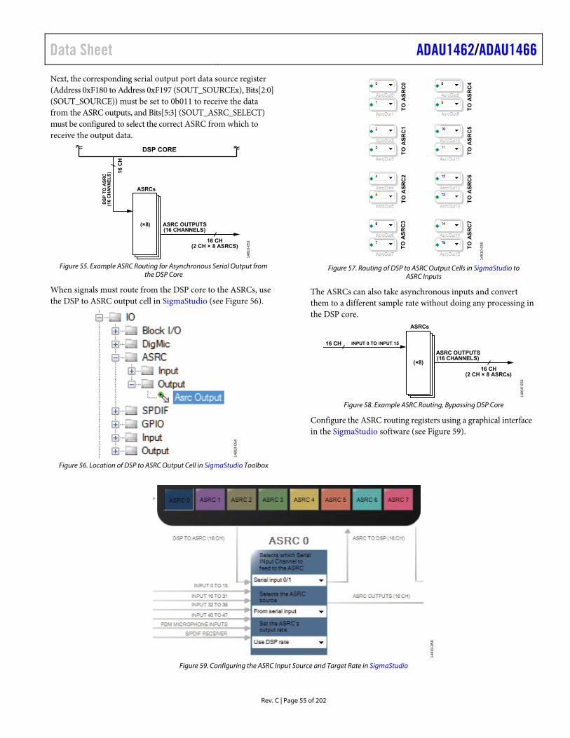
Data Sheet ADAU1462/ADAU1466
Rev. C | Page 55 of 202
Next, the corresponding serial output port data source register (Address 0xF180 to Address 0xF197 (SOUT_SOURCEx), Bits[2:0] (SOUT_SOURCE)) must be set to 0b011 to receive the data from the ASRC outputs, and Bits[5:3] (SOUT_ASRC_SELECT) must be configured to select the correct ASRC from which to receive the output data.
DSP CORE
ASRCs
(×8) ASRC OUTPUTS(16 CHANNELS)
16 CH(2 CH × 8 ASRCS)
16 C
H
DS
P T
O A
SR
C(1
6 C
HA
NN
EL
S)
1481
0-05
3
Figure 55. Example ASRC Routing for Asynchronous Serial Output from
the DSP Core
When signals must route from the DSP core to the ASRCs, use the DSP to ASRC output cell in SigmaStudio (see Figure 56).
1481
0-05
4
Figure 56. Location of DSP to ASRC Output Cell in SigmaStudio Toolbox
TO
AS
RC
0T
O A
SR
C1
TO
AS
RC
2T
O A
SR
C3
TO
AS
RC
4T
O A
SR
C5
TO
AS
RC
6T
O A
SR
C7
148
10-
05
5
Figure 57. Routing of DSP to ASRC Output Cells in SigmaStudio to
ASRC Inputs
The ASRCs can also take asynchronous inputs and convert them to a different sample rate without doing any processing in the DSP core.
ASRCs
(×8)
INPUT 0 TO INPUT 15
ASRC OUTPUTS(16 CHANNELS)
16 CH(2 CH × 8 ASRCs)
16 CH
1481
0-0
56
Figure 58. Example ASRC Routing, Bypassing DSP Core
Configure the ASRC routing registers using a graphical interface in the SigmaStudio software (see Figure 59).
148
10-0
58
Figure 59. Configuring the ASRC Input Source and Target Rate in SigmaStudio
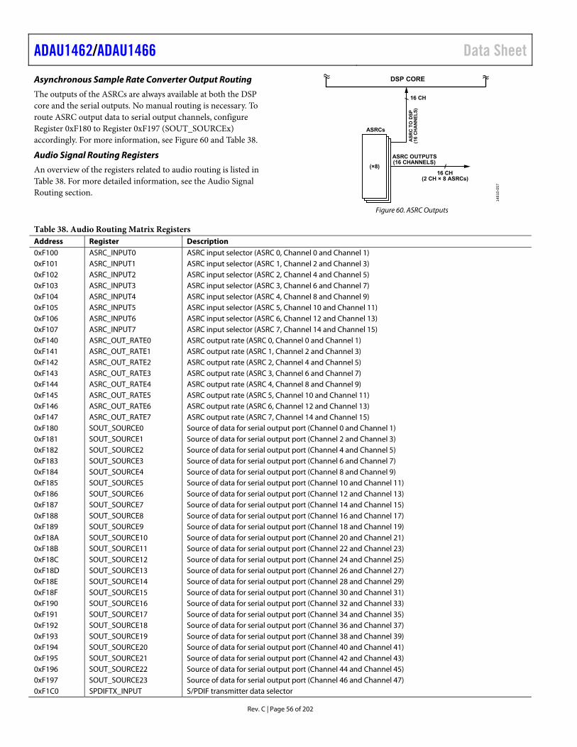
ADAU1462/ADAU1466 Data Sheet
Rev. C | Page 56 of 202
Asynchronous Sample Rate Converter Output Routing
The outputs of the ASRCs are always available at both the DSP core and the serial outputs. No manual routing is necessary. To route ASRC output data to serial output channels, configure Register 0xF180 to Register 0xF197 (SOUT_SOURCEx) accordingly. For more information, see Figure 60 and Table 38.
Audio Signal Routing Registers
An overview of the registers related to audio routing is listed in Table 38. For more detailed information, see the Audio Signal Routing section.
ASRCs
(×8)
ASRC OUTPUTS(16 CHANNELS)
16 CH(2 CH × 8 ASRCs)
16 CH
AS
RC
TO
DS
P(1
6 C
HA
NN
EL
S)
DSP CORE
148
10-0
57
Figure 60. ASRC Outputs
Table 38. Audio Routing Matrix Registers Address Register Description 0xF100 ASRC_INPUT0 ASRC input selector (ASRC 0, Channel 0 and Channel 1) 0xF101 ASRC_INPUT1 ASRC input selector (ASRC 1, Channel 2 and Channel 3) 0xF102 ASRC_INPUT2 ASRC input selector (ASRC 2, Channel 4 and Channel 5) 0xF103 ASRC_INPUT3 ASRC input selector (ASRC 3, Channel 6 and Channel 7) 0xF104 ASRC_INPUT4 ASRC input selector (ASRC 4, Channel 8 and Channel 9) 0xF105 ASRC_INPUT5 ASRC input selector (ASRC 5, Channel 10 and Channel 11) 0xF106 ASRC_INPUT6 ASRC input selector (ASRC 6, Channel 12 and Channel 13) 0xF107 ASRC_INPUT7 ASRC input selector (ASRC 7, Channel 14 and Channel 15) 0xF140 ASRC_OUT_RATE0 ASRC output rate (ASRC 0, Channel 0 and Channel 1) 0xF141 ASRC_OUT_RATE1 ASRC output rate (ASRC 1, Channel 2 and Channel 3) 0xF142 ASRC_OUT_RATE2 ASRC output rate (ASRC 2, Channel 4 and Channel 5) 0xF143 ASRC_OUT_RATE3 ASRC output rate (ASRC 3, Channel 6 and Channel 7) 0xF144 ASRC_OUT_RATE4 ASRC output rate (ASRC 4, Channel 8 and Channel 9) 0xF145 ASRC_OUT_RATE5 ASRC output rate (ASRC 5, Channel 10 and Channel 11) 0xF146 ASRC_OUT_RATE6 ASRC output rate (ASRC 6, Channel 12 and Channel 13) 0xF147 ASRC_OUT_RATE7 ASRC output rate (ASRC 7, Channel 14 and Channel 15) 0xF180 SOUT_SOURCE0 Source of data for serial output port (Channel 0 and Channel 1) 0xF181 SOUT_SOURCE1 Source of data for serial output port (Channel 2 and Channel 3) 0xF182 SOUT_SOURCE2 Source of data for serial output port (Channel 4 and Channel 5) 0xF183 SOUT_SOURCE3 Source of data for serial output port (Channel 6 and Channel 7) 0xF184 SOUT_SOURCE4 Source of data for serial output port (Channel 8 and Channel 9) 0xF185 SOUT_SOURCE5 Source of data for serial output port (Channel 10 and Channel 11) 0xF186 SOUT_SOURCE6 Source of data for serial output port (Channel 12 and Channel 13) 0xF187 SOUT_SOURCE7 Source of data for serial output port (Channel 14 and Channel 15) 0xF188 SOUT_SOURCE8 Source of data for serial output port (Channel 16 and Channel 17) 0xF189 SOUT_SOURCE9 Source of data for serial output port (Channel 18 and Channel 19) 0xF18A SOUT_SOURCE10 Source of data for serial output port (Channel 20 and Channel 21) 0xF18B SOUT_SOURCE11 Source of data for serial output port (Channel 22 and Channel 23) 0xF18C SOUT_SOURCE12 Source of data for serial output port (Channel 24 and Channel 25) 0xF18D SOUT_SOURCE13 Source of data for serial output port (Channel 26 and Channel 27) 0xF18E SOUT_SOURCE14 Source of data for serial output port (Channel 28 and Channel 29) 0xF18F SOUT_SOURCE15 Source of data for serial output port (Channel 30 and Channel 31) 0xF190 SOUT_SOURCE16 Source of data for serial output port (Channel 32 and Channel 33) 0xF191 SOUT_SOURCE17 Source of data for serial output port (Channel 34 and Channel 35) 0xF192 SOUT_SOURCE18 Source of data for serial output port (Channel 36 and Channel 37) 0xF193 SOUT_SOURCE19 Source of data for serial output port (Channel 38 and Channel 39) 0xF194 SOUT_SOURCE20 Source of data for serial output port (Channel 40 and Channel 41) 0xF195 SOUT_SOURCE21 Source of data for serial output port (Channel 42 and Channel 43) 0xF196 SOUT_SOURCE22 Source of data for serial output port (Channel 44 and Channel 45) 0xF197 SOUT_SOURCE23 Source of data for serial output port (Channel 46 and Channel 47) 0xF1C0 SPDIFTX_INPUT S/PDIF transmitter data selector
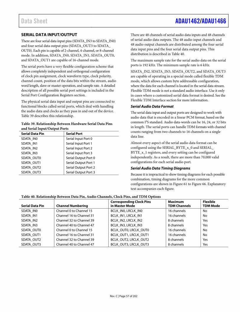
Data Sheet ADAU1462/ADAU1466
Rev. C | Page 57 of 202
SERIAL DATA INPUT/OUTPUT There are four serial data input pins (SDATA_IN3 to SDATA_IN0) and four serial data output pins (SDATA_OUT3 to SDATA_ OUT0). Each pin is capable of 2-channel, 4-channel, or 8-channel mode. In addition, SDATA_IN0, SDATA_IN1, SDATA_OUT0, and SDATA_OUT1 are capable of 16-channel mode.
The serial ports have a very flexible configuration scheme that allows completely independent and orthogonal configuration of clock pin assignment, clock waveform type, clock polarity, channel count, position of the data bits within the stream, audio word length, slave or master operation, and sample rate. A detailed description of all possible serial port settings is included in the Serial Port Configuration Registers section.
The physical serial data input and output pins are connected to functional blocks called serial ports, which deal with handling the audio data and clocks as they pass in and out of the device. Table 39 describes this relationship.
Table 39. Relationship Between Hardware Serial Data Pins and Serial Input/Output Ports Serial Data Pin Serial Port SDATA_IN0 Serial Input Port 0 SDATA_IN1 Serial Input Port 1 SDATA_IN2 Serial Input Port 2 SDATA_IN3 Serial Input Port 3 SDATA_OUT0 Serial Output Port 0 SDATA_OUT1 Serial Output Port 1 SDATA_OUT2 Serial Output Port 2 SDATA_OUT3 Serial Output Port 3
There are 48 channels of serial audio data inputs and 48 channels of serial audio data outputs. The 48 audio input channels and 48 audio output channels are distributed among the four serial data input pins and the four serial data output pins. This distribution is described in Table 40.
The maximum sample rate for the serial audio data on the serial ports is 192 kHz. The minimum sample rate is 6 kHz.
SDATA_IN2, SDATA_IN3, SDATA_OUT2, and SDATA_OUT3 are capable of operating in a special mode called flexible TDM mode, which allows custom byte addressable configuration, where the data for each channel is located in the serial data stream. Flexible TDM mode is not a standard audio interface. Use it only in cases where a customized serial data format is desired. See the Flexible TDM Interface section for more information.
Serial Audio Data Format
The serial data input and output ports are designed to work with audio data that is encoded in a linear PCM format, based on the common I2S standard. Audio data-words can be 16, 24, or 32 bits in length. The serial ports can handle TDM formats with channel counts ranging from two channels to 16 channels on a single data line.
Almost every aspect of the serial audio data format can be configured using the SERIAL_BYTE_x_0 and SERIAL_ BYTE_x_1 registers, and every setting can be configured independently. As a result, there are more than 70,000 valid configurations for each serial audio port.
Serial Audio Data Timing Diagrams
Because it is impractical to show timing diagrams for each possible combination, timing diagrams for the more common configurations are shown in Figure 61 to Figure 66. Explanatory text accompanies each figure.
Table 40. Relationship Between Data Pin, Audio Channels, Clock Pins, and TDM Options
Serial Data Pin Channel Numbering Corresponding Clock Pins in Master Mode
Maximum TDM Channels
Flexible TDM Mode
SDATA_IN0 Channel 0 to Channel 15 BCLK_IN0, LRCLK_IN0 16 channels No SDATA_IN1 Channel 16 to Channel 31 BCLK_IN1, LRCLK_IN1 16 channels No SDATA_IN2 Channel 32 to Channel 39 BCLK_IN2, LRCLK_IN2 8 channels Yes SDATA_IN3 Channel 40 to Channel 47 BCLK_IN3, LRCLK_IN3 8 channels Yes SDATA_OUT0 Channel 0 to Channel 15 BCLK_OUT0, LRCLK_OUT0 16 channels No SDATA_OUT1 Channel 16 to Channel 31 BCLK_OUT1, LRCLK_OUT1 16 channels No SDATA_OUT2 Channel 32 to Channel 39 BCLK_OUT2, LRCLK_OUT2 8 channels Yes SDATA_OUT3 Channel 40 to Channel 47 BCLK_OUT3, LRCLK_OUT3 8 channels Yes
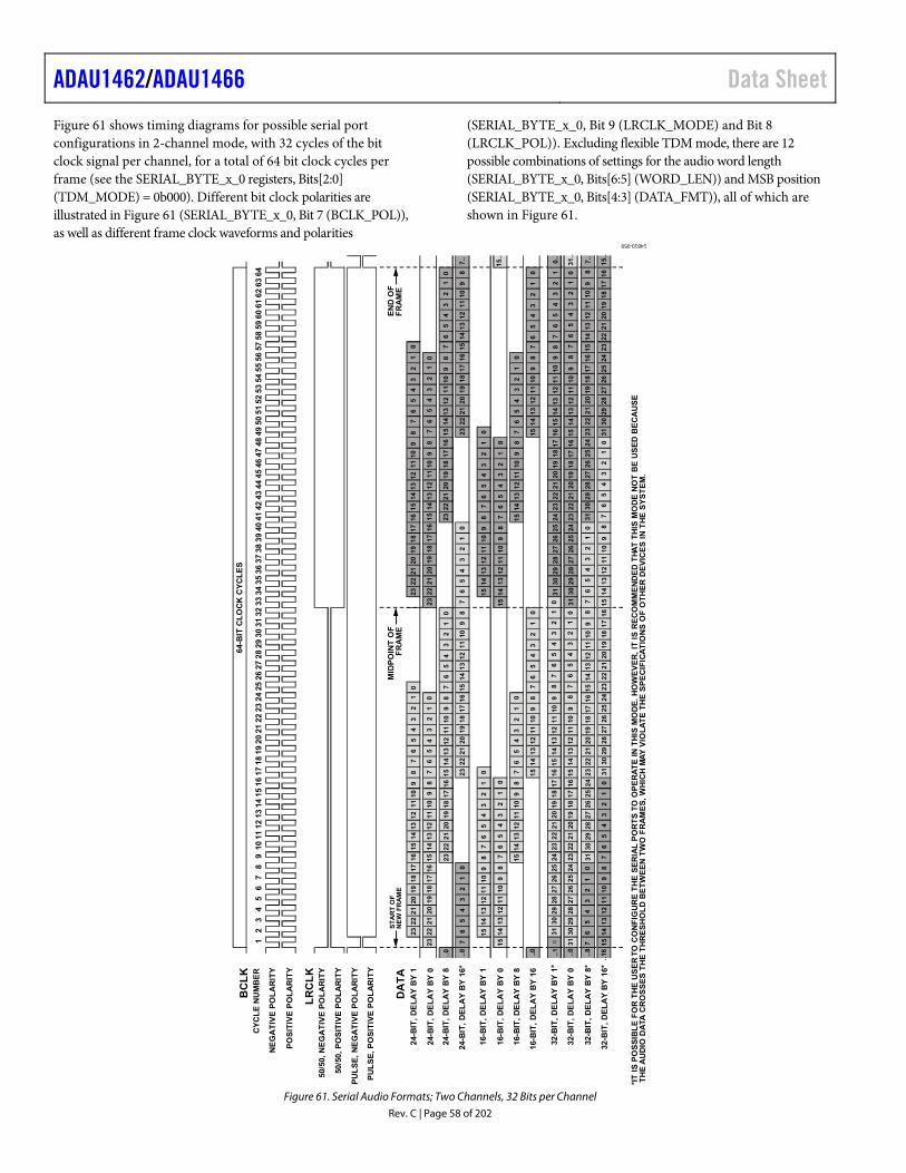
ADAU1462/ADAU1466 Data Sheet
Rev. C | Page 58 of 202
Figure 61 shows timing diagrams for possible serial port configurations in 2-channel mode, with 32 cycles of the bit clock signal per channel, for a total of 64 bit clock cycles per frame (see the SERIAL_BYTE_x_0 registers, Bits[2:0] (TDM_MODE) = 0b000). Different bit clock polarities are illustrated in Figure 61 (SERIAL_BYTE_x_0, Bit 7 (BCLK_POL)), as well as different frame clock waveforms and polarities
(SERIAL_BYTE_x_0, Bit 9 (LRCLK_MODE) and Bit 8 (LRCLK_POL)). Excluding flexible TDM mode, there are 12 possible combinations of settings for the audio word length (SERIAL_BYTE_x_0, Bits[6:5] (WORD_LEN)) and MSB position (SERIAL_BYTE_x_0, Bits[4:3] (DATA_FMT)), all of which are shown in Figure 61.
BC
LK
..0 ..0
..16..8
76
54
32
10
54
32
10
98
76
..8
..1
076
54
32
10
CY
CL
E N
UM
BE
R
NE
GA
TIV
E P
OL
AR
ITY
PO
SIT
IVE
PO
LA
RIT
Y
LR
CL
K50
/50,
NE
GA
TIV
E P
OL
AR
ITY
50/5
0, P
OS
ITIV
E P
OL
AR
ITY
PU
LS
E,
NE
GA
TIV
E P
OL
AR
ITY
PU
LS
E,
PO
SIT
IVE
PO
LA
RIT
Y
DA
TA
ST
AR
T O
FN
EW
FR
AM
E
24-B
IT,
DE
LA
Y B
Y 1
24-B
IT,
DE
LA
Y B
Y 0
24-B
IT,
DE
LA
Y B
Y 8
24-B
IT,
DE
LA
Y B
Y 1
6*
16-B
IT,
DE
LA
Y B
Y 1
16-B
IT,
DE
LA
Y B
Y 0
16-B
IT,
DE
LA
Y B
Y 8
16-B
IT,
DE
LA
Y B
Y 1
6
32-B
IT,
DE
LA
Y B
Y 1
*
32-B
IT,
DE
LA
Y B
Y 0
32-B
IT,
DE
LA
Y B
Y 8
*
32-B
IT,
DE
LA
Y B
Y 1
6*
EN
D O
FF
RA
ME
MID
PO
INT
OF
FR
AM
E
64-B
IT C
LO
CK
CY
CL
ES
12
34
56
78
910
1112
1314
1516
1718
1920
3132
3334
3536
3738
3941
4243
4445
4647
4849
4051
5253
5455
5657
5859
5061
6263
6460
2122
23
10
23
45
67
89
10
11
12
1314
1516
17
18
19
20
21
22
23
2425
2627
2829
30
10
23
45
67
89
10
11
12
13
14
15
16
17
18
19
20
21
2223
10
23
45
67
89
10
11
12
13
14
15
16
17
18
19
2021
22
23
10
23
45
67
89
10
11
1213
14
1516
17
18
19
20
21
22
23
..0
10
23
45
67
89
10
11
12
13
14
15
10
23
45
67
89
10
11
12
1314
15
10
23
45
67
89
10
1112
13
14
15
10
23
45
67
89
1011
12
1314
1516
17
18
19
20
2122
23
10
23
45
67
89
10
11
12
13
14
15
16
17
1819
20
21
22
23
10
23
45
67
89
10
11
12
13
14
15
1617
18
19
20
21
22
23
7..
15..
15..
7..
31..
0..
89
10
11
12
13
14
15
16
17
18
19
20
2122
23
10
23
45
67
89
10
11
12
13
14
15
10
23
45
67
89
10
11
12
13
14
15
10
23
45
67
89
10
11
1213
14
15
10
23
45
67
89
10
11
12
13
14
15
10
23
45
67
89
10
11
1213
14
15
10
23
45
67
89
10
11
12
13
14
15
10
11
12
13
14
15
16
17
18
19
20
21
22
2324
25
26
27
28
29
31
30
54
32
10
98
76
10
11
12
13
14
15
16
17
18
19
20
21
2223
24
25
26
27
28
29
31
30
54
32
10
98
76
10
11
12
13
14
15
16
17
18
19
20
21
22
23
24
25
26
27
28
2931
30
54
32
19
87
610
1112
13
14
15
16
17
18
19
20
21
22
23
24
25
2627
28
29
31
30
54
32
10
98
76
10
1112
13
14
15
16
17
18
19
20
21
22
23
24
2526
27
28
29
31
30
98
10
11
1213
1415
16
17
18
19
20
21
22
23
24
25
26
2728
29
31
30
16
17
18
19
20
21
22
23
24
25
26
27
28
2931
30
54
32
10
98
76
10
11
12
13
14
15
16
17
1819
20
21
22
23
24
25
26
27
28
2931
30
*IT
IS
PO
SS
IBL
E F
OR
TH
E U
SE
RT
O C
ON
FIG
UR
E T
HE
SE
RIA
L P
OR
TS
TO
OP
ER
AT
E I
N T
HIS
MO
DE
. H
OW
EV
ER
, IT
IS
RE
CO
MM
EN
DE
D T
HA
T T
HIS
MO
DE
NO
T B
E U
SE
D B
EC
AU
SE
TH
EA
UD
IO D
ATA
CR
OS
SE
S T
HE
TH
RE
SH
OL
D B
ET
WE
EN
TW
O F
RA
ME
S,
WH
ICH
MA
Y V
IOL
AT
E T
HE
SP
EC
IFIC
AT
ION
S O
F O
TH
ER
DE
VIC
ES
IN
TH
E S
YS
TE
M.
14810-059
Figure 61. Serial Audio Formats; Two Channels, 32 Bits per Channel
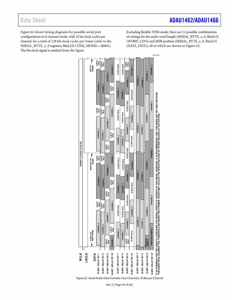
Data Sheet ADAU1462/ADAU1466
Rev. C | Page 59 of 202
Figure 62 shows timing diagrams for possible serial port configurations in 4-channel mode, with 32 bit clock cycles per channel, for a total of 128 bit clock cycles per frame (refer to the SERIAL_BYTE_x_0 registers, Bits[2:0] (TDM_MODE) = 0b001). The bit clock signal is omitted from the figure.
Excluding flexible TDM mode, there are 12 possible combinations of settings for the audio word length (SERIAL_BYTE_x_0, Bits[6:5] (WORD_LEN)) and MSB position (SERIAL_BYTE_x_0, Bits[4:3] (DATA_FMT)), all of which are shown in Figure 62.
ST
AR
T O
FN
EW
FR
AM
EE
ND
OF
FR
AM
EM
IDP
OIN
T O
FF
RA
ME
24-B
IT,
DE
LA
Y B
Y 1
16-B
IT,
DE
LA
Y B
Y 1
24-B
IT,
DE
LA
Y B
Y 0
24-B
IT,
DE
LA
Y B
Y 8
24-B
IT,
DE
LA
Y B
Y 1
6*
16-B
IT,
DE
LA
Y B
Y 0
16-B
IT,
DE
LA
Y B
Y 8
16-B
IT,
DE
LA
Y B
Y 1
6
32-B
IT,
DE
LA
Y B
Y 1
*
32-B
IT,
DE
LA
Y B
Y 0
32-B
IT,
DE
LA
Y B
Y 8
*
32-B
IT,
DE
LA
Y B
Y 1
6*
BC
LK
LR
CL
K
DA
TA
128-
BIT
CL
OC
K C
YC
LE
S
8 B
ITS
IDL
E
8 B
ITS
IDL
E
8 B
ITS
IDL
E
8 B
ITS
IDL
E
8 B
ITS
IDL
E
8 B
ITS
IDL
E
8 B
ITS
IDL
E
8 B
ITS
IDL
E
8 B
ITS
IDL
E
8 B
ITS
IDL
E8
BIT
SID
LE
8 B
ITS
IDL
E
8 B
ITS
IDL
E
8 B
ITS
IDL
E
8 B
ITS
IDL
E8
BIT
SID
LE
8 B
ITS
IDL
E
8 B
ITS
IDL
E
16 B
ITS
ID
LE
16 B
ITS
ID
LE
16 B
ITS
ID
LE
16 B
ITS
ID
LE
16 B
ITS
ID
LE
16 B
ITS
ID
LE
16 B
ITS
ID
LE
16 B
ITS
ID
LE
16 B
ITS
ID
LE
16 B
ITS
ID
LE
16 B
ITS
ID
LE
16 B
ITS
ID
LE
16 B
ITS
ID
LE
16 B
ITS
ID
LE
16 B
ITS
ID
LE
CH
AN
NE
L 3
CH
AN
NE
L 0
CH
AN
NE
L 0
CH
AN
NE
L 0
CH
AN
NE
L 0
CH
AN
NE
L 0
CH
AN
NE
L 0
CH
AN
NE
L 0
CH
AN
NE
L 0
CH
AN
NE
L 1
CH
AN
NE
L 1
CH
AN
NE
L 1
CH
AN
NE
L 2
CH
AN
NE
L 2
CH
AN
NE
L 2
CH
AN
NE
L 2
CH
AN
NE
L 2
CH
AN
NE
L 2
CH
AN
NE
L 2
CH
AN
NE
L 2
CH
AN
NE
L 2
CH
AN
NE
L 2
CH
AN
NE
L 2
CH
AN
NE
L 2
CH
AN
NE
L 3
CH
AN
NE
L 3
CH
AN
NE
L 3
CH
AN
NE
L 3
CH
AN
NE
L 3
CH
AN
NE
L 3
CH
AN
NE
L 3
CH
AN
NE
L 3
CH
AN
NE
L 3
CH
AN
NE
L 3
CH
AN
NE
L 3
CH
AN
NE
L 3
CH
AN
NE
L 1
CH
AN
NE
L 1
CH
AN
NE
L 1
CH
AN
NE
L 1
CH
AN
NE
L 1
CH
AN
NE
L 1
CH
AN
NE
L 1
CH
AN
NE
L 1
CH
AN
NE
L 1
CH
AN
NE
L 0
CH
AN
NE
L 0
CH
AN
NE
L 0
CH
AN
NE
L 0
PR
EV
IOU
S S
AM
PL
E
PR
EV
IOU
SS
AM
PL
E
*IT
IS
PO
SS
IBL
E F
OR
TH
E U
SE
RT
O C
ON
FIG
UR
E T
HE
SE
RIA
L P
OR
TS
TO
OP
ER
AT
E I
N T
HIS
MO
DE
. H
OW
EV
ER
, IT
IS
RE
CO
MM
EN
DE
D T
HAT
TH
IS M
OD
E N
OT
BE
US
ED
BE
CA
US
E T
HE
AU
DIO
DA
TA C
RO
SS
ES
TH
E T
HR
ES
HO
LD
BE
TW
EE
N T
WO
FR
AM
ES
, W
HIC
H M
AY
VIO
LA
TE
TH
E S
PE
CIF
ICA
TIO
NS
OF
OT
HE
R D
EV
ICE
S I
N T
HE
SY
ST
EM
.
14810-060
Figure 62. Serial Audio Data Formats; Four Channels, 32 Bits per Channel
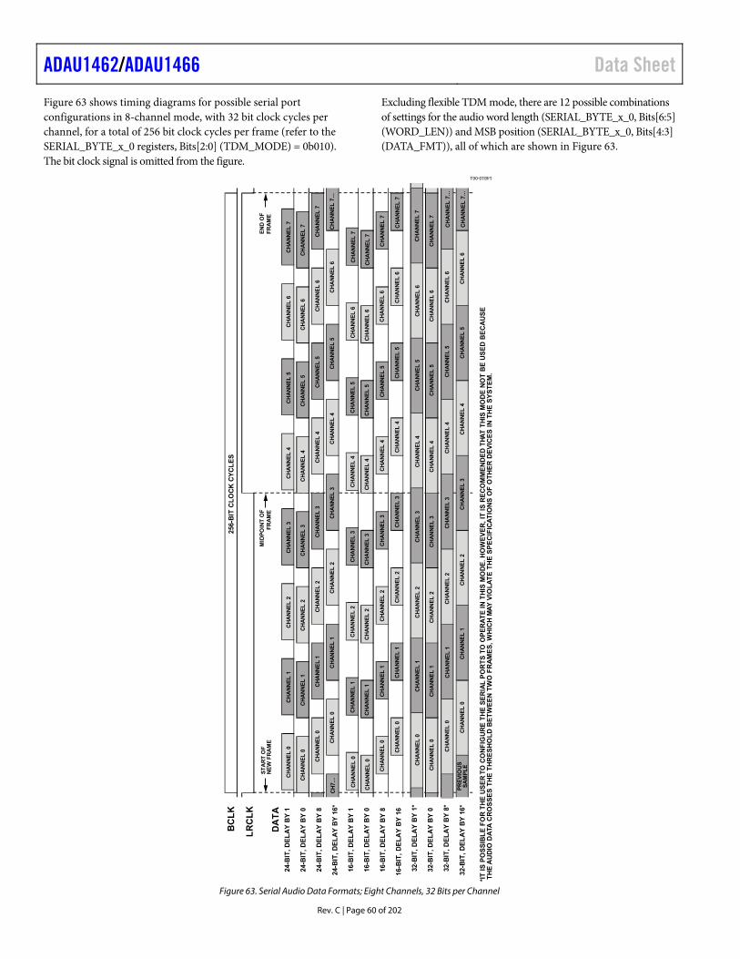
ADAU1462/ADAU1466 Data Sheet
Rev. C | Page 60 of 202
Figure 63 shows timing diagrams for possible serial port configurations in 8-channel mode, with 32 bit clock cycles per channel, for a total of 256 bit clock cycles per frame (refer to the SERIAL_BYTE_x_0 registers, Bits[2:0] (TDM_MODE) = 0b010). The bit clock signal is omitted from the figure.
Excluding flexible TDM mode, there are 12 possible combinations of settings for the audio word length (SERIAL_BYTE_x_0, Bits[6:5] (WORD_LEN)) and MSB position (SERIAL_BYTE_x_0, Bits[4:3] (DATA_FMT)), all of which are shown in Figure 63.
ST
AR
T O
FN
EW
FR
AM
EE
ND
OF
FR
AM
EM
IDP
OIN
T O
FF
RA
ME
24-B
IT,
DE
LA
Y B
Y 1
24-B
IT,
DE
LA
Y B
Y 0
24-B
IT,
DE
LA
Y B
Y 8
24-B
IT,
DE
LA
Y B
Y 1
6*
16-B
IT,
DE
LA
Y B
Y 1
16-B
IT,
DE
LA
Y B
Y 0
16-B
IT,
DE
LA
Y B
Y 8
16-B
IT,
DE
LA
Y B
Y 1
6
32-B
IT,
DE
LA
Y B
Y 1
*
32-B
IT,
DE
LA
Y B
Y 0
32-B
IT,
DE
LA
Y B
Y 8
*
32-B
IT,
DE
LA
Y B
Y 1
6*
BC
LK
LR
CL
K
DA
TA
256-
BIT
CL
OC
K C
YC
LE
S
CH
AN
NE
L 0
CH
AN
NE
L 0
CH
AN
NE
L 0
CH
AN
NE
L 0
CH
AN
NE
L 0
CH
7...
CH
AN
NE
L 0
CH
AN
NE
L 0
CH
AN
NE
L 0
CH
AN
NE
L 1
CH
AN
NE
L 1
CH
AN
NE
L 1
CH
AN
NE
L 1
CH
AN
NE
L 1
CH
AN
NE
L 1
CH
AN
NE
L 1
CH
AN
NE
L 1
CH
AN
NE
L 2
CH
AN
NE
L 2
CH
AN
NE
L 2
CH
AN
NE
L 2
CH
AN
NE
L 3
CH
AN
NE
L 3
CH
AN
NE
L 3
CH
AN
NE
L 3
CH
AN
NE
L 4
CH
AN
NE
L 4
CH
AN
NE
L 4
CH
AN
NE
L 4
CH
AN
NE
L 5
CH
AN
NE
L 5
CH
AN
NE
L 5
CH
AN
NE
L 5
CH
AN
NE
L 2
CH
AN
NE
L 2
CH
AN
NE
L 2
CH
AN
NE
L 2
CH
AN
NE
L 3
CH
AN
NE
L 3
CH
AN
NE
L 3
CH
AN
NE
L 3
CH
AN
NE
L 4
CH
AN
NE
L 4
CH
AN
NE
L 4
CH
AN
NE
L 4
CH
AN
NE
L 5
CH
AN
NE
L 5
CH
AN
NE
L 5
CH
AN
NE
L 5
CH
AN
NE
L 6
CH
AN
NE
L 6
CH
AN
NE
L 6
CH
AN
NE
L 6
CH
AN
NE
L 6
CH
AN
NE
L 6
CH
AN
NE
L 6
CH
AN
NE
L 6
CH
AN
NE
L 6
CH
AN
NE
L 6
CH
AN
NE
L 6
CH
AN
NE
L 6
CH
AN
NE
L 5
CH
AN
NE
L 5
CH
AN
NE
L 5
CH
AN
NE
L 5
CH
AN
NE
L 4
CH
AN
NE
L 4
CH
AN
NE
L 4
CH
AN
NE
L 4
CH
AN
NE
L 3
CH
AN
NE
L 3
CH
AN
NE
L 3
CH
AN
NE
L 3
CH
AN
NE
L 2
CH
AN
NE
L 2
CH
AN
NE
L 2
CH
AN
NE
L 2
CH
AN
NE
L 1
CH
AN
NE
L 1
CH
AN
NE
L 1
CH
AN
NE
L 1
CH
AN
NE
L 0
CH
AN
NE
L 0
CH
AN
NE
L 0
CH
AN
NE
L 0
CH
AN
NE
L 7
CH
AN
NE
L 7
CH
AN
NE
L 7
CH
AN
NE
L 7
...
CH
AN
NE
L 7
CH
AN
NE
L 7
CH
AN
NE
L 7
...
CH
AN
NE
L 7
...
CH
AN
NE
L 7
CH
AN
NE
L 7
CH
AN
NE
L 7
CH
AN
NE
L 7
PR
EV
IOU
SS
AM
PL
E
*IT
IS
PO
SS
IBL
E F
OR
TH
E U
SE
RT
O C
ON
FIG
UR
E T
HE
SE
RIA
L P
OR
TS
TO
OP
ER
AT
E I
N T
HIS
MO
DE
. H
OW
EV
ER
, IT
IS
RE
CO
MM
EN
DE
D T
HAT
TH
IS M
OD
E N
OT
BE
US
ED
BE
CA
US
E T
HE
AU
DIO
DA
TA C
RO
SS
ES
TH
E T
HR
ES
HO
LD
BE
TW
EE
N T
WO
FR
AM
ES
, W
HIC
H M
AY
VIO
LA
TE
TH
E S
PE
CIF
ICA
TIO
NS
OF
OT
HE
R D
EV
ICE
S I
N T
HE
SY
ST
EM
.
14810-061
Figure 63. Serial Audio Data Formats; Eight Channels, 32 Bits per Channel
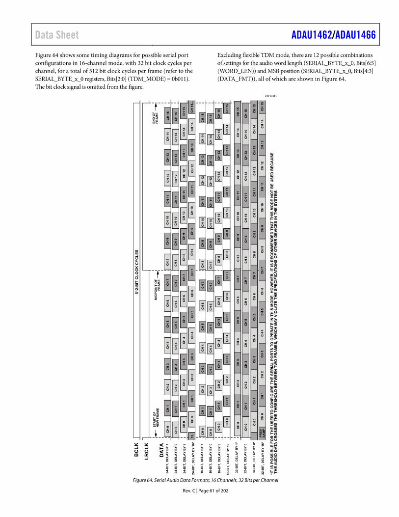
Data Sheet ADAU1462/ADAU1466
Rev. C | Page 61 of 202
Figure 64 shows some timing diagrams for possible serial port configurations in 16-channel mode, with 32 bit clock cycles per channel, for a total of 512 bit clock cycles per frame (refer to the SERIAL_BYTE_x_0 registers, Bits[2:0] (TDM_MODE) = 0b011). The bit clock signal is omitted from the figure.
Excluding flexible TDM mode, there are 12 possible combinations of settings for the audio word length (SERIAL_BYTE_x_0, Bits[6:5] (WORD_LEN)) and MSB position (SERIAL_BYTE_x_0, Bits[4:3] (DATA_FMT)), all of which are shown in Figure 64.
ST
AR
T O
FN
EW
FR
AM
EE
ND
OF
FR
AM
EM
IDP
OIN
T O
FF
RA
ME
24-B
IT,
DE
LA
Y B
Y 1
16-B
IT,
DE
LA
Y B
Y 1
32-
BIT
, D
EL
AY
BY
1*
32-B
IT,
DE
LA
Y B
Y 0
32-
BIT
, D
EL
AY
BY
8*
32-
BIT
, D
EL
AY
BY
16*
24-B
IT,
DE
LA
Y B
Y 0
24-B
IT,
DE
LA
Y B
Y 8
24-
BIT
, D
EL
AY
BY
16*
16-B
IT,
DE
LA
Y B
Y 0
16-B
IT,
DE
LA
Y B
Y 8
16-B
IT,
DE
LA
Y B
Y 1
6
BC
LK
LR
CL
K
DA
TA
CH
0CH
0
CH
0
CH
0
CH
0
CH
1
CH
1
CH
1
CH
1
CH
2
CH
2
CH
2
CH
2
CH
3
CH
3
CH
3
CH
3
CH
0
CH
0
CH
0
CH
0
CH
1
CH
1
CH
1
CH
1
CH
2
CH
2
CH
2
CH
2
CH
3
CH
3
CH
3
CH
3
CH
4
CH
4
CH
4
CH
4
CH
5
CH
5
CH
5
CH
5
CH
6
CH
6
CH
6
CH
6
CH
7
CH
7
CH
7
CH
7
CH
4
CH
4
CH
4
CH
4
CH
5
CH
5
CH
5
CH
5
CH
6
CH
6
CH
6
CH
6
CH
7
CH
7
CH
7
CH
7
CH
8
CH
8
CH
8
CH
8
CH
9
CH
9
CH
9
CH
9
CH
0 CH
0 CH
0
CH
1
CH
1 CH
1 CH
1
CH
2
CH
2 CH
2 CH
2
CH
3
CH
3 CH
3 CH
3
CH
4
CH
4 CH
4 CH
4
CH
5
CH
5 CH
5 CH
5
CH
6
CH
6 CH
6 CH
6
CH
7
CH
7 CH
7 CH
7
CH
8
CH
8 CH
8 CH
8
CH
9
CH
9 CH
9 CH
9
CH
10
CH
10
CH
10
CH
10
CH
8
CH
8
CH
8
CH
8
CH
9
CH
9
CH
9
CH
9
CH
10
CH
10
CH
10
CH
10
CH
10
CH
10
CH
10
CH
10
CH
11
CH
11
CH
11
CH
11
CH
11
CH
11
CH
11
CH
11
CH
11
CH
11
CH
11
CH
11
CH
12
CH
12
CH
12
CH
12
CH
12
CH
12
CH
12
CH
12
CH
12
CH
12
CH
12
CH
12
CH
13
CH
13
CH
13
CH
13
CH
13
CH
13
CH
13
CH
13
CH
13
CH
13
CH
13
CH
13
CH
14
CH
14
CH
14
CH
14
CH
14
CH
14
CH
14
CH
14
CH
14
CH
14
CH
14
CH
15
CH
15
CH
15
CH
15
CH
15.
..
CH
15
CH
15
CH
15
CH
15
CH
15
CH
15
CH
15
CH
14
PR
EV
SA
MP
..1
5
512-
BIT
CL
OC
K C
YC
LE
S
*IT
IS
PO
SS
IBL
E F
OR
TH
E U
SE
RT
O C
ON
FIG
UR
E T
HE
SE
RIA
L P
OR
TS
TO
OP
ER
AT
E I
N T
HIS
MO
DE
. H
OW
EV
ER
, IT
IS
RE
CO
MM
EN
DE
D T
HA
T T
HIS
MO
DE
NO
T B
E U
SE
D B
EC
AU
SE
TH
EA
UD
IO D
ATA
CR
OS
SE
S T
HE
TH
RE
SH
OL
D B
ET
WE
EN
TW
O F
RA
ME
S,
WH
ICH
MA
Y V
IOL
AT
E T
HE
SP
EC
IFIC
AT
ION
S O
F O
TH
ER
DE
VIC
ES
IN
TH
E S
YS
TE
M.
14810-062
Figure 64. Serial Audio Data Formats; 16 Channels, 32 Bits per Channel
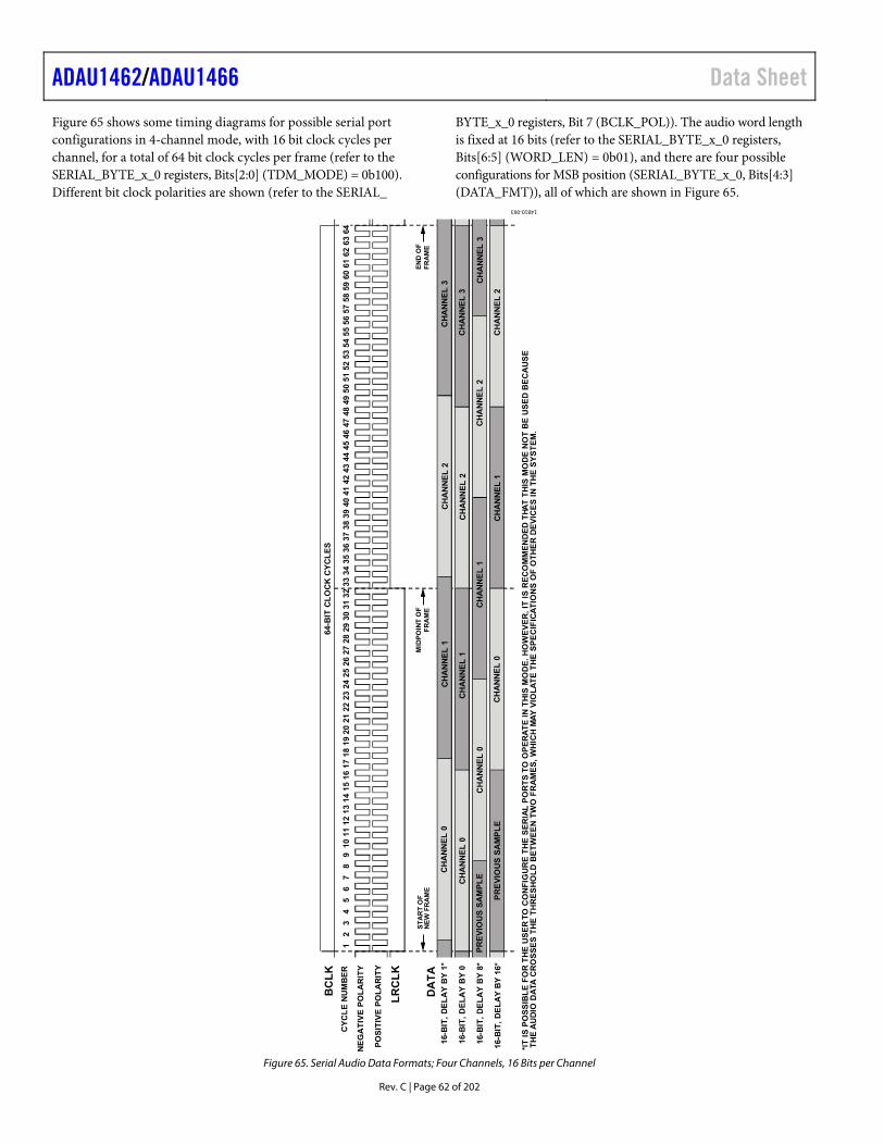
ADAU1462/ADAU1466 Data Sheet
Rev. C | Page 62 of 202
Figure 65 shows some timing diagrams for possible serial port configurations in 4-channel mode, with 16 bit clock cycles per channel, for a total of 64 bit clock cycles per frame (refer to the SERIAL_BYTE_x_0 registers, Bits[2:0] (TDM_MODE) = 0b100). Different bit clock polarities are shown (refer to the SERIAL_
BYTE_x_0 registers, Bit 7 (BCLK_POL)). The audio word length is fixed at 16 bits (refer to the SERIAL_BYTE_x_0 registers, Bits[6:5] (WORD_LEN) = 0b01), and there are four possible configurations for MSB position (SERIAL_BYTE_x_0, Bits[4:3] (DATA_FMT)), all of which are shown in Figure 65.
BC
LK
CY
CL
E N
UM
BE
R
NE
GA
TIV
E P
OL
AR
ITY
PO
SIT
IVE
PO
LA
RIT
Y
LR
CL
K
DA
TA
16-B
IT,
DE
LA
Y B
Y 1
*
16-B
IT,
DE
LA
Y B
Y 0
16-B
IT,
DE
LA
Y B
Y 8
*
16-B
IT,
DE
LA
Y B
Y 1
6*
ST
AR
T O
FN
EW
FR
AM
EE
ND
OF
FR
AM
EM
IDP
OIN
T O
FF
RA
ME
12
34
56
78
910
1112
1314
1516
1718
1920
3132
3334
3536
3738
3941
4243
4445
4647
4849
4051
5253
5455
5657
5859
5061
6263
6021
2223
2425
2627
2829
30
64-B
IT C
LO
CK
CY
CL
ES
CH
AN
NE
L 1
CH
AN
NE
L 1
CH
AN
NE
L 1
CH
AN
NE
L 1
CH
AN
NE
L 2
CH
AN
NE
L 2
CH
AN
NE
L 2
CH
AN
NE
L 2
CH
AN
NE
L 3
CH
AN
NE
L 3
CH
AN
NE
L 3
CH
AN
NE
L 0
CH
AN
NE
L 0
CH
AN
NE
L 0
CH
AN
NE
L 0
PR
EV
IOU
S S
AM
PL
E
PR
EV
IOU
S S
AM
PL
E
64
*IT
IS
PO
SS
IBL
E F
OR
TH
E U
SE
RT
O C
ON
FIG
UR
E T
HE
SE
RIA
L P
OR
TS
TO
OP
ER
AT
E I
N T
HIS
MO
DE
. H
OW
EV
ER
, IT
IS
RE
CO
MM
EN
DE
D T
HA
T T
HIS
MO
DE
NO
T B
E U
SE
D B
EC
AU
SE
TH
EA
UD
IO D
ATA
CR
OS
SE
S T
HE
TH
RE
SH
OL
D B
ET
WE
EN
TW
O F
RA
ME
S,
WH
ICH
MA
Y V
IOL
AT
E T
HE
SP
EC
IFIC
AT
ION
S O
F O
TH
ER
DE
VIC
ES
IN
TH
E S
YS
TE
M.
14810-063
Figure 65. Serial Audio Data Formats; Four Channels, 16 Bits per Channel
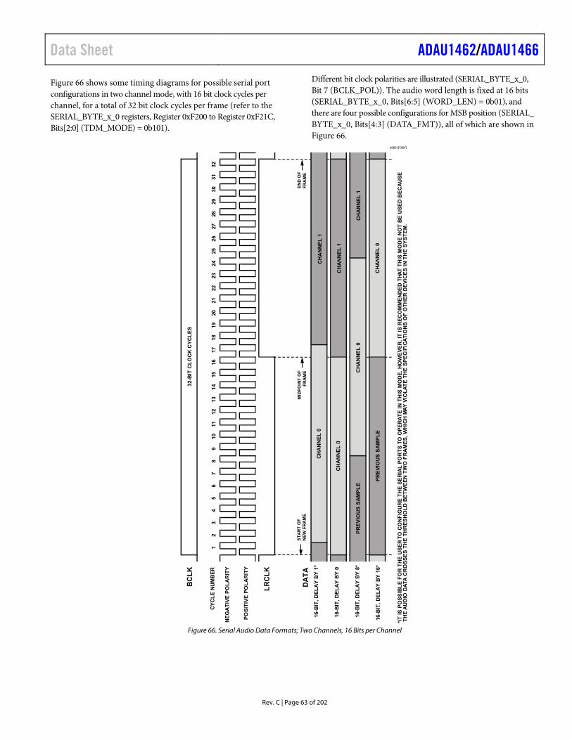
Data Sheet ADAU1462/ADAU1466
Rev. C | Page 63 of 202
Figure 66 shows some timing diagrams for possible serial port configurations in two channel mode, with 16 bit clock cycles per channel, for a total of 32 bit clock cycles per frame (refer to the SERIAL_BYTE_x_0 registers, Register 0xF200 to Register 0xF21C, Bits[2:0] (TDM_MODE) = 0b101).
Different bit clock polarities are illustrated (SERIAL_BYTE_x_0, Bit 7 (BCLK_POL)). The audio word length is fixed at 16 bits (SERIAL_BYTE_x_0, Bits[6:5] (WORD_LEN) = 0b01), and there are four possible configurations for MSB position (SERIAL_ BYTE_x_0, Bits[4:3] (DATA_FMT)), all of which are shown in Figure 66.
BC
LK
CY
CL
E N
UM
BE
R
NE
GA
TIV
E P
OL
AR
ITY
PO
SIT
IVE
PO
LA
RIT
Y
LR
CL
K
DA
TA
16-B
IT,
DE
LA
Y B
Y 1
*
16-B
IT,
DE
LA
Y B
Y 0
16-B
IT,
DE
LA
Y B
Y 8
*
16-B
IT,
DE
LA
Y B
Y 1
6*
ST
AR
T O
FN
EW
FR
AM
EM
IDP
OIN
T O
FF
RA
ME
12
34
56
78
910
1112
1314
1516
1718
1920
3132
2122
2324
2526
2728
2930
32-B
IT C
LO
CK
CY
CL
ES
EN
D O
FF
RA
ME
CH
AN
NE
L 0
CH
AN
NE
L 0
CH
AN
NE
L 0
CH
AN
NE
L 1
CH
AN
NE
L 1
CH
AN
NE
L 1
PR
EV
IOU
S S
AM
PL
E
PR
EV
IOU
S S
AM
PL
EC
HA
NN
EL
0
*IT
IS
PO
SS
IBL
E F
OR
TH
E U
SE
RT
O C
ON
FIG
UR
E T
HE
SE
RIA
L P
OR
TS
TO
OP
ER
AT
E I
N T
HIS
MO
DE
. H
OW
EV
ER
, IT
IS
RE
CO
MM
EN
DE
D T
HAT
TH
IS M
OD
E N
OT
BE
US
ED
BE
CA
US
E T
HE
AU
DIO
DA
TA C
RO
SS
ES
TH
E T
HR
ES
HO
LD
BE
TW
EE
N T
WO
FR
AM
ES
, W
HIC
H M
AY
VIO
LA
TE
TH
E S
PE
CIF
ICA
TIO
NS
OF
OT
HE
R D
EV
ICE
S I
N T
HE
SY
ST
EM
.
14810-064
Figure 66. Serial Audio Data Formats; Two Channels, 16 Bits per Channel
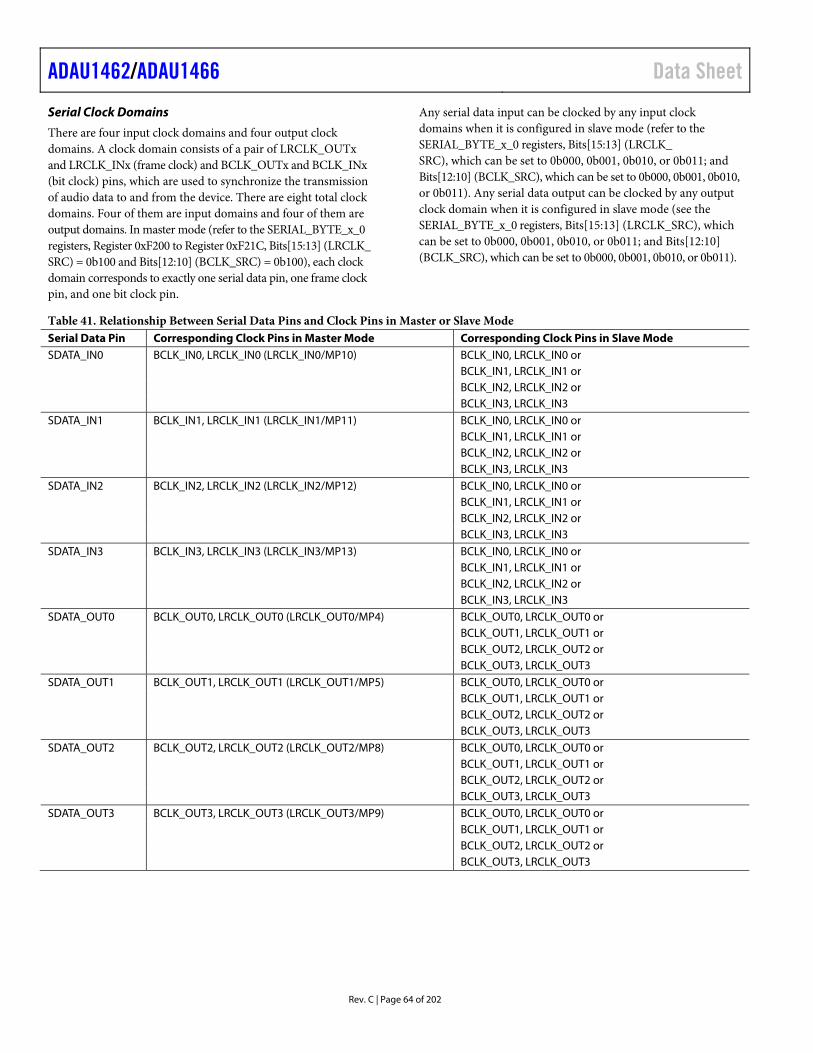
ADAU1462/ADAU1466 Data Sheet
Rev. C | Page 64 of 202
Serial Clock Domains
There are four input clock domains and four output clock domains. A clock domain consists of a pair of LRCLK_OUTx and LRCLK_INx (frame clock) and BCLK_OUTx and BCLK_INx (bit clock) pins, which are used to synchronize the transmission of audio data to and from the device. There are eight total clock domains. Four of them are input domains and four of them are output domains. In master mode (refer to the SERIAL_BYTE_x_0 registers, Register 0xF200 to Register 0xF21C, Bits[15:13] (LRCLK_ SRC) = 0b100 and Bits[12:10] (BCLK_SRC) = 0b100), each clock domain corresponds to exactly one serial data pin, one frame clock pin, and one bit clock pin.
Any serial data input can be clocked by any input clock domains when it is configured in slave mode (refer to the SERIAL_BYTE_x_0 registers, Bits[15:13] (LRCLK_ SRC), which can be set to 0b000, 0b001, 0b010, or 0b011; and Bits[12:10] (BCLK_SRC), which can be set to 0b000, 0b001, 0b010, or 0b011). Any serial data output can be clocked by any output clock domain when it is configured in slave mode (see the SERIAL_BYTE_x_0 registers, Bits[15:13] (LRCLK_SRC), which can be set to 0b000, 0b001, 0b010, or 0b011; and Bits[12:10] (BCLK_SRC), which can be set to 0b000, 0b001, 0b010, or 0b011).
Table 41. Relationship Between Serial Data Pins and Clock Pins in Master or Slave Mode Serial Data Pin Corresponding Clock Pins in Master Mode Corresponding Clock Pins in Slave Mode SDATA_IN0 BCLK_IN0, LRCLK_IN0 (LRCLK_IN0/MP10) BCLK_IN0, LRCLK_IN0 or BCLK_IN1, LRCLK_IN1 or BCLK_IN2, LRCLK_IN2 or BCLK_IN3, LRCLK_IN3 SDATA_IN1 BCLK_IN1, LRCLK_IN1 (LRCLK_IN1/MP11) BCLK_IN0, LRCLK_IN0 or BCLK_IN1, LRCLK_IN1 or BCLK_IN2, LRCLK_IN2 or BCLK_IN3, LRCLK_IN3 SDATA_IN2 BCLK_IN2, LRCLK_IN2 (LRCLK_IN2/MP12) BCLK_IN0, LRCLK_IN0 or BCLK_IN1, LRCLK_IN1 or BCLK_IN2, LRCLK_IN2 or BCLK_IN3, LRCLK_IN3 SDATA_IN3 BCLK_IN3, LRCLK_IN3 (LRCLK_IN3/MP13) BCLK_IN0, LRCLK_IN0 or BCLK_IN1, LRCLK_IN1 or BCLK_IN2, LRCLK_IN2 or BCLK_IN3, LRCLK_IN3 SDATA_OUT0 BCLK_OUT0, LRCLK_OUT0 (LRCLK_OUT0/MP4) BCLK_OUT0, LRCLK_OUT0 or BCLK_OUT1, LRCLK_OUT1 or BCLK_OUT2, LRCLK_OUT2 or BCLK_OUT3, LRCLK_OUT3 SDATA_OUT1 BCLK_OUT1, LRCLK_OUT1 (LRCLK_OUT1/MP5) BCLK_OUT0, LRCLK_OUT0 or BCLK_OUT1, LRCLK_OUT1 or BCLK_OUT2, LRCLK_OUT2 or BCLK_OUT3, LRCLK_OUT3 SDATA_OUT2 BCLK_OUT2, LRCLK_OUT2 (LRCLK_OUT2/MP8) BCLK_OUT0, LRCLK_OUT0 or BCLK_OUT1, LRCLK_OUT1 or BCLK_OUT2, LRCLK_OUT2 or BCLK_OUT3, LRCLK_OUT3 SDATA_OUT3 BCLK_OUT3, LRCLK_OUT3 (LRCLK_OUT3/MP9) BCLK_OUT0, LRCLK_OUT0 or BCLK_OUT1, LRCLK_OUT1 or BCLK_OUT2, LRCLK_OUT2 or BCLK_OUT3, LRCLK_OUT3
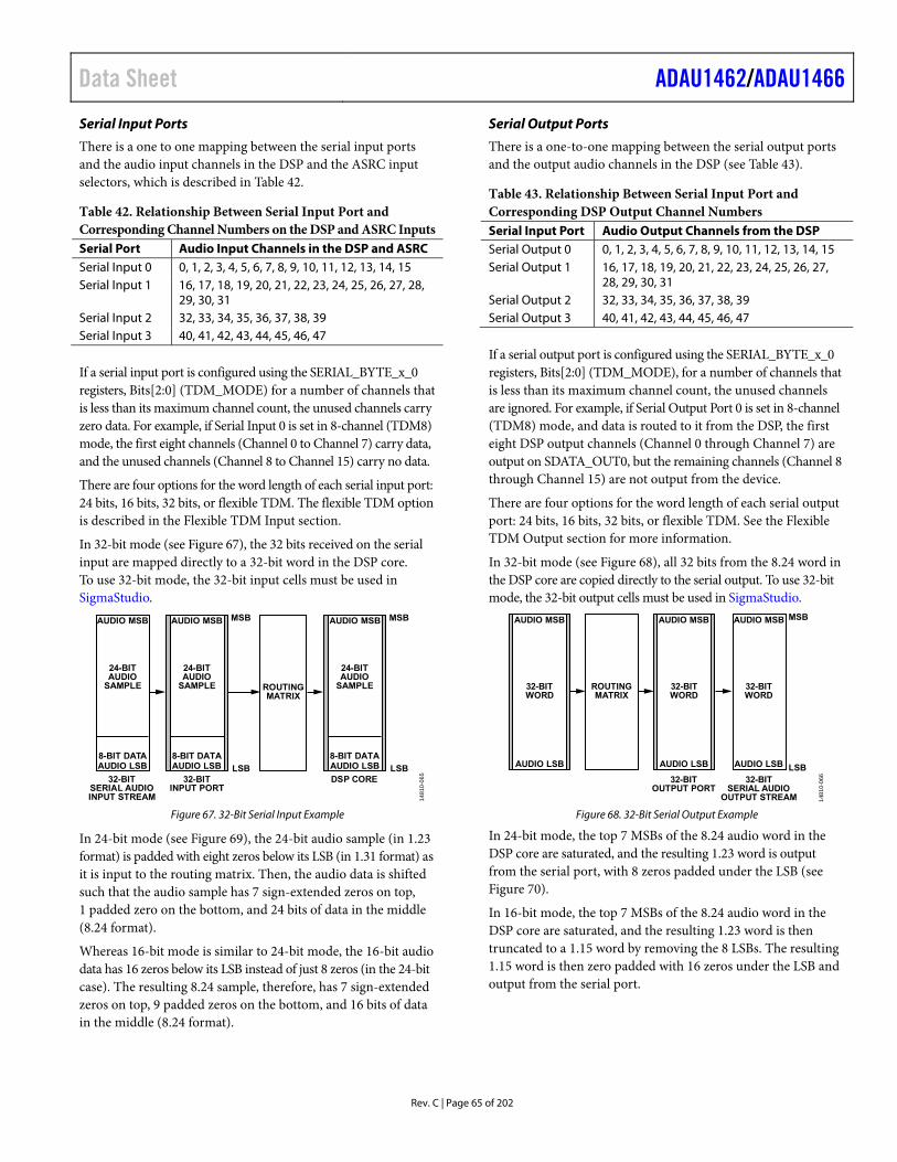
Data Sheet ADAU1462/ADAU1466
Rev. C | Page 65 of 202
Serial Input Ports
There is a one to one mapping between the serial input ports and the audio input channels in the DSP and the ASRC input selectors, which is described in Table 42.
Table 42. Relationship Between Serial Input Port and Corresponding Channel Numbers on the DSP and ASRC Inputs Serial Port Audio Input Channels in the DSP and ASRC Serial Input 0 0, 1, 2, 3, 4, 5, 6, 7, 8, 9, 10, 11, 12, 13, 14, 15 Serial Input 1 16, 17, 18, 19, 20, 21, 22, 23, 24, 25, 26, 27, 28,
29, 30, 31 Serial Input 2 32, 33, 34, 35, 36, 37, 38, 39 Serial Input 3 40, 41, 42, 43, 44, 45, 46, 47
If a serial input port is configured using the SERIAL_BYTE_x_0 registers, Bits[2:0] (TDM_MODE) for a number of channels that is less than its maximum channel count, the unused channels carry zero data. For example, if Serial Input 0 is set in 8-channel (TDM8) mode, the first eight channels (Channel 0 to Channel 7) carry data, and the unused channels (Channel 8 to Channel 15) carry no data.
There are four options for the word length of each serial input port: 24 bits, 16 bits, 32 bits, or flexible TDM. The flexible TDM option is described in the Flexible TDM Input section.
In 32-bit mode (see Figure 67), the 32 bits received on the serial input are mapped directly to a 32-bit word in the DSP core. To use 32-bit mode, the 32-bit input cells must be used in SigmaStudio.
24-BITAUDIO
SAMPLE
8-BIT DATA
ROUTINGMATRIX
24-BITAUDIO
SAMPLE
LSB32-BIT
INPUT PORT32-BIT
SERIAL AUDIOINPUT STREAM
8-BIT DATA
24-BITAUDIO
SAMPLE
8-BIT DATA
LSB
MSB MSB
DSP CORE
AUDIO LSB
AUDIO MSB
AUDIO LSB
AUDIO MSB
AUDIO LSB
AUDIO MSB
14
810
-06
5
Figure 67. 32-Bit Serial Input Example
In 24-bit mode (see Figure 69), the 24-bit audio sample (in 1.23 format) is padded with eight zeros below its LSB (in 1.31 format) as it is input to the routing matrix. Then, the audio data is shifted such that the audio sample has 7 sign-extended zeros on top, 1 padded zero on the bottom, and 24 bits of data in the middle (8.24 format).
Whereas 16-bit mode is similar to 24-bit mode, the 16-bit audio data has 16 zeros below its LSB instead of just 8 zeros (in the 24-bit case). The resulting 8.24 sample, therefore, has 7 sign-extended zeros on top, 9 padded zeros on the bottom, and 16 bits of data in the middle (8.24 format).
Serial Output Ports
There is a one-to-one mapping between the serial output ports and the output audio channels in the DSP (see Table 43).
Table 43. Relationship Between Serial Input Port and Corresponding DSP Output Channel Numbers Serial Input Port Audio Output Channels from the DSP Serial Output 0 0, 1, 2, 3, 4, 5, 6, 7, 8, 9, 10, 11, 12, 13, 14, 15 Serial Output 1 16, 17, 18, 19, 20, 21, 22, 23, 24, 25, 26, 27,
28, 29, 30, 31 Serial Output 2 32, 33, 34, 35, 36, 37, 38, 39 Serial Output 3 40, 41, 42, 43, 44, 45, 46, 47
If a serial output port is configured using the SERIAL_BYTE_x_0 registers, Bits[2:0] (TDM_MODE), for a number of channels that is less than its maximum channel count, the unused channels are ignored. For example, if Serial Output Port 0 is set in 8-channel (TDM8) mode, and data is routed to it from the DSP, the first eight DSP output channels (Channel 0 through Channel 7) are output on SDATA_OUT0, but the remaining channels (Channel 8 through Channel 15) are not output from the device.
There are four options for the word length of each serial output port: 24 bits, 16 bits, 32 bits, or flexible TDM. See the Flexible TDM Output section for more information.
In 32-bit mode (see Figure 68), all 32 bits from the 8.24 word in the DSP core are copied directly to the serial output. To use 32-bit mode, the 32-bit output cells must be used in SigmaStudio.
ROUTINGMATRIX
32-BITWORD
32-BITWORD
32-BITWORD
32-BITOUTPUT PORT
LSB
MSB
32-BITSERIAL AUDIO
OUTPUT STREAM
AUDIO LSB
AUDIO MSB
AUDIO LSB
AUDIO MSB
AUDIO LSB
AUDIO MSB
148
10
-066
Figure 68. 32-Bit Serial Output Example
In 24-bit mode, the top 7 MSBs of the 8.24 audio word in the DSP core are saturated, and the resulting 1.23 word is output from the serial port, with 8 zeros padded under the LSB (see Figure 70).
In 16-bit mode, the top 7 MSBs of the 8.24 audio word in the DSP core are saturated, and the resulting 1.23 word is then truncated to a 1.15 word by removing the 8 LSBs. The resulting 1.15 word is then zero padded with 16 zeros under the LSB and output from the serial port.
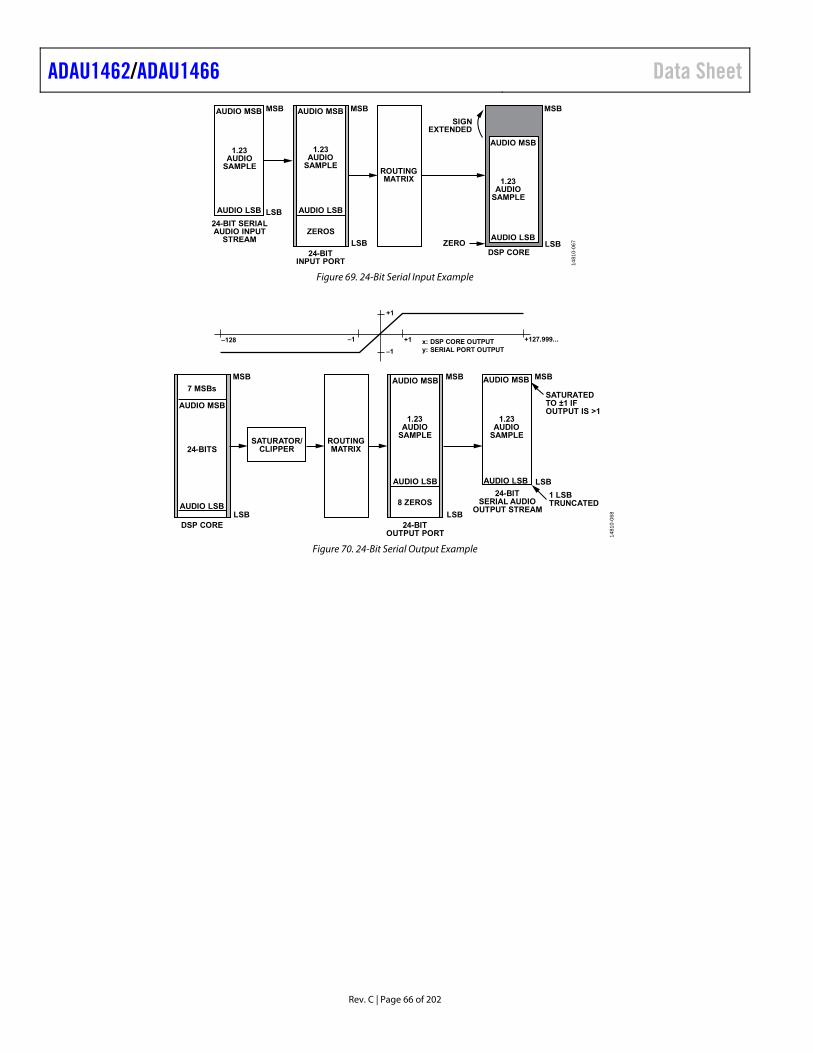
ADAU1462/ADAU1466 Data Sheet
Rev. C | Page 66 of 202
1.23AUDIO
SAMPLE
24-BIT SERIALAUDIO INPUT
STREAM
ROUTINGMATRIX
1.23AUDIO
SAMPLE
LSB
ZEROS
1.23AUDIO
SAMPLE
LSB
MSB
SIGNEXTENDED
ZERO
MSB
DSP CORE
LSB
MSB
24-BITINPUT PORT
AUDIO LSB
AUDIO MSB
AUDIO LSB
AUDIO MSB
AUDIO LSB
AUDIO MSB
1481
0-06
7
Figure 69. 24-Bit Serial Input Example
ROUTINGMATRIX
1.23AUDIO
SAMPLE
1.23AUDIO
SAMPLE
8 ZEROS
AUDIO LSB
AUDIO MSB
LSB
MSB
LSB
MSB
24-BITOUTPUT PORT
24-BITSERIAL AUDIO
OUTPUT STREAM
24-BITS
7 MSBs
LSB
MSB
DSP CORE
SATURATEDTO ±1 IFOUTPUT IS >1
1 LSBTRUNCATED
SATURATOR/CLIPPER
+1
+1
–1
–1–128 +127.999...x: DSP CORE OUTPUTy: SERIAL PORT OUTPUT
AUDIO LSB
AUDIO MSB
AUDIO LSB
AUDIO MSB
14
81
0-0
68
Figure 70. 24-Bit Serial Output Example
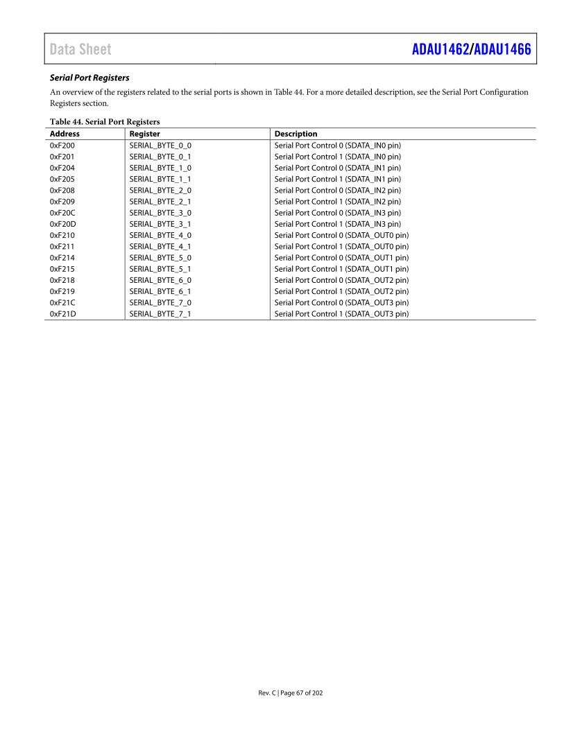
Data Sheet ADAU1462/ADAU1466
Rev. C | Page 67 of 202
Serial Port Registers
An overview of the registers related to the serial ports is shown in Table 44. For a more detailed description, see the Serial Port Configuration Registers section.
Table 44. Serial Port Registers Address Register Description 0xF200 SERIAL_BYTE_0_0 Serial Port Control 0 (SDATA_IN0 pin) 0xF201 SERIAL_BYTE_0_1 Serial Port Control 1 (SDATA_IN0 pin) 0xF204 SERIAL_BYTE_1_0 Serial Port Control 0 (SDATA_IN1 pin) 0xF205 SERIAL_BYTE_1_1 Serial Port Control 1 (SDATA_IN1 pin) 0xF208 SERIAL_BYTE_2_0 Serial Port Control 0 (SDATA_IN2 pin) 0xF209 SERIAL_BYTE_2_1 Serial Port Control 1 (SDATA_IN2 pin) 0xF20C SERIAL_BYTE_3_0 Serial Port Control 0 (SDATA_IN3 pin) 0xF20D SERIAL_BYTE_3_1 Serial Port Control 1 (SDATA_IN3 pin) 0xF210 SERIAL_BYTE_4_0 Serial Port Control 0 (SDATA_OUT0 pin) 0xF211 SERIAL_BYTE_4_1 Serial Port Control 1 (SDATA_OUT0 pin) 0xF214 SERIAL_BYTE_5_0 Serial Port Control 0 (SDATA_OUT1 pin) 0xF215 SERIAL_BYTE_5_1 Serial Port Control 1 (SDATA_OUT1 pin) 0xF218 SERIAL_BYTE_6_0 Serial Port Control 0 (SDATA_OUT2 pin) 0xF219 SERIAL_BYTE_6_1 Serial Port Control 1 (SDATA_OUT2 pin) 0xF21C SERIAL_BYTE_7_0 Serial Port Control 0 (SDATA_OUT3 pin) 0xF21D SERIAL_BYTE_7_1 Serial Port Control 1 (SDATA_OUT3 pin)
ADAU1462/ADAU1466 Data Sheet
Rev. C | Page 68 of 202
FLEXIBLE TDM INTERFACE The flexible TDM interface is available as an optional mode of operation on the SDATA_IN2 and SDATA_IN3 serial input ports, as well as on the SDATA_OUT2 and SDATA_OUT3 serial output ports. To use flexible TDM mode, the corresponding serial ports must be set in flexible TDM mode (SERIAL_BYTE_x_0 register, Bits[6:5] (WORD_LEN) = 0b11 and SERIAL_BYTE_x_0 register, Bits[2:0] = 0b010). Flexible TDM input mode requires that both SDATA_IN2 and SDATA_IN3 be configured for flexible TDM mode. Likewise, flexible TDM output mode requires that both SDATA_OUT2 and SDATA_OUT3 pins be configured for flexible TDM mode.
The flexible TDM interface provides byte addressable data place-ment in the input and output data streams on the corresponding serial data input/output pins. Each data stream is configured like a standard 8-channel TDM interface, with a total of 256 data bits (or 32 bytes) in the span of an audio frame. Because flexible TDM mode runs on two pins simultaneously, and each pin has 32 bytes of data, this means that there are a total of 64 data bytes. In flexible TDM input mode, each input channel inside the device can select its source data from any of the 64 input data bytes. In flexible TDM output mode, any serial output channel can be routed to any of the 64 output data bytes.
Flexible TDM Input
In flexible TDM input mode, two 256-bit data streams are input to the SDATA_IN2 and SDATA_IN3 pins. These 256 bits of data compose eight channels of four bytes each, for a total of 32 bytes on each pin, and a total of 64 bytes when both input pins are combined. The flexible TDM input functional block routes the desired input byte to a given byte in the serial input channels. Those serial input channels are then available as normal audio data in the audio routing matrix. The data can be passed to the DSP core, the ASRC inputs, or the serial outputs as needed.
There are a total of 64 control registers (FTDM_INx) that can be configured to set up the mapping of input data bytes to the corresponding bytes in the serial input channels. Each byte in each serial input channel has a corresponding control register, which selects the incoming data byte on the serial input pins that must be mapped to it. Figure 71 shows, from left to right, the data streams entering the serial input pins, the serial input channels, and the registers (see FTDM_INx, Register 0xF300 to Register 0xF33F) that correspond to each byte in the serial input channels.
Flexible TDM Output
In flexible TDM output mode, two 256-bit data streams are output from the SDATA_OUT2 and SDATA_OUT3 pins. These 256 bits of data compose eight channels of four bytes each, for a total of 32 bytes on each pin, and a total of 64 bytes when both input pins are combined. The flexible TDM output functional block routes the desired byte from the desired serial output channel to a given byte in the output streams. The serial output channels originate from the audio routing matrix, which is configured using the SOUT_SOURCEx control registers.
There are a total of 64 control registers (see FTDM_OUTx, Register 0xF388 to Register 0xF3BF) that can be configured to set up the mapping of the bytes in the serial output channels and the bytes in the data streams exiting the serial output pins. Each byte in the data streams being output from the serial output pins has a corresponding control register, which selects the desired byte from the desired serial output channel. Figure 72 shows, from left to right, the serial output channels originating from the routing matrix, the serial output pins and data streams, and the control registers (FTDM_OUTx) that correspond to each byte in the serial output data streams.
Data Sheet ADAU1462/ADAU1466
Rev. C | Page 69 of 202
BIT
SS
ER
IAL
PO
RT
SIN
PU
T D
AT
A S
TR
EA
MS
[31:
24]
BIT
S[2
3:16
]B
ITS
[15:
8]B
ITS
[7:0
]
SE
RIA
LIN
PU
TC
HA
NNE
L32
FLEXIBLE TDM BLOCK
FT
DM
_IN
0→
SE
RIA
LIN
PU
TC
HA
NNE
L33
FT
DM
_IN
4→
SE
RIA
LIN
PU
TC
HA
NNE
L34
FT
DM
_IN
8→
SE
RIA
LIN
PU
TC
HA
NNE
L35
FT
DM
_IN
12→
SE
RIA
LIN
PU
TC
HA
NNE
L36
FT
DM
_IN
16→
SE
RIA
LIN
PU
TC
HA
NNE
L37
FT
DM
_IN
20→
SE
RIA
LIN
PU
TC
HA
NNE
L38
FT
DM
_IN
24→
SE
RIA
LIN
PU
TC
HA
NNE
L39
FT
DM
_IN
28→
SE
RIA
LIN
PU
TC
HA
NNE
L40
FT
DM
_IN
32→
SE
RIA
LIN
PU
TC
HA
NNE
L41
FT
DM
_IN
36→
SE
RIA
LIN
PU
TC
HA
NNE
L42
FT
DM
_IN
40→
SE
RIA
LIN
PU
TC
HA
NNE
L43
FT
DM
_IN
44→
SE
RIA
LIN
PU
TC
HA
NNE
L44
FT
DM
_IN
48→
SE
RIA
LIN
PU
TC
HA
NNE
L45
FT
DM
_IN
52→
SE
RIA
LIN
PU
TC
HA
NNE
L46
FT
DM
_IN
56→
SE
RIA
LIN
PU
TC
HA
NNE
L47
FT
DM
_IN
60
FT
DM
_IN
1F
TD
M_I
N5
FT
DM
_IN
9F
TD
M_I
N13
FT
DM
_IN
17F
TD
M_I
N21
FT
DM
_IN
25F
TD
M_I
N29
FT
DM
_IN
33F
TD
M_I
N37
FT
DM
_IN
41F
TD
M_I
N45
FT
DM
_IN
49F
TD
M_I
N53
FT
DM
_IN
57
FT
DM
_IN
2F
TD
M_I
N6
FT
DM
_IN
10F
TD
M_I
N14
FT
DM
_IN
18F
TD
M_I
N22
FT
DM
_IN
26F
TD
M_I
N30
FT
DM
_IN
34F
TD
M_I
N38
FT
DM
_IN
42F
TD
M_I
N46
FT
DM
_IN
50F
TD
M_I
N54
FT
DM
_IN
58
FT
DM
_IN
3F
TD
M_I
N7
FT
DM
_IN
11F
TD
M_I
N15
FT
DM
_IN
19F
TD
M_I
N23
FT
DM
_IN
27F
TD
M_I
N31
FT
DM
_IN
35F
TD
M_I
N39
FT
DM
_IN
43F
TD
M_I
N47
FT
DM
_IN
51F
TD
M_I
N55
FT
DM
_IN
59F
TD
M_I
N61
FT
DM
_IN
62F
TD
M_I
N63
→
SD
AT
A_I
N2
CH
AN
NE
L 7
01
23
CH
AN
NE
L 6
01
23
CH
AN
NE
L 5
01
23
CH
AN
NE
L 4
01
23
CH
AN
NE
L 3
01
23
CH
AN
NE
L 2
01
23
CH
AN
NE
L 1
01
23
CH
AN
NE
L 0
01
23
SD
AT
A_I
N3
CH
AN
NE
L 7
01
23
CH
AN
NE
L 6
01
23
CH
AN
NE
L 5
01
23
CH
AN
NE
L 4
01
23
CH
AN
NE
L 3
01
23
CH
AN
NE
L 2
01
23
CH
AN
NE
L 1
01
23
CH
AN
NE
L 0
01
23
14810-069
Figure 71. Flexible TDM Input Mapping
ADAU1462/ADAU1466 Data Sheet
Rev. C | Page 70 of 202
BIT
S[3
1:24
]B
ITS
[23:
16]
BIT
S[1
5:8]
BIT
S[7
:0]
SE
RIA
L O
UT
PU
T C
HA
NN
EL
32
01
23
→
SE
RIA
L O
UT
PU
T C
HA
NN
EL
33
01
23
→
SE
RIA
L O
UT
PU
T C
HA
NN
EL
34
01
23
→
SE
RIA
L O
UT
PU
T C
HA
NN
EL
35
01
23
→
SE
RIA
L O
UT
PU
T C
HA
NN
EL
36
01
23
→
SE
RIA
L O
UT
PU
T C
HA
NN
EL
37
01
23
→
SE
RIA
L O
UT
PU
T C
HA
NN
EL
38
01
23
→
SE
RIA
L O
UT
PU
T C
HA
NN
EL
39
01
23
→
SE
RIA
L O
UT
PU
T C
HA
NN
EL
40
01
23
→
SE
RIA
L O
UT
PU
T C
HA
NN
EL
41
01
23
→
SE
RIA
L O
UT
PU
T C
HA
NN
EL
42
01
23
→
SE
RIA
L O
UT
PU
T C
HA
NN
EL
43
01
23
→
SE
RIA
L O
UT
PU
T C
HA
NN
EL
44
01
23
→
SE
RIA
L O
UT
PU
T C
HA
NN
EL
45
01
23
→
SE
RIA
L O
UT
PU
T C
HA
NN
EL
46
01
23
→
SE
RIA
L O
UT
PU
T C
HA
NN
EL
47
01
23
→
TD
M8
CH
AN
NE
L
BY
TE
FTDM_OUT0
FTDM_OUT1
FTDM_OUT2
FTDM_OUT3
FTDM_OUT4
FTDM_OUT5
FTDM_OUT6
FTDM_OUT7
FTDM_OUT8
FTDM_OUT9
FTDM_OUT10
FTDM_OUT11
FTDM_OUT12
FTDM_OUT13
FTDM_OUT14
FTDM_OUT15
FTDM_OUT16
FTDM_OUT17
FTDM_OUT18
FTDM_OUT19
FTDM_OUT20
FTDM_OUT21
FTDM_OUT22
FTDM_OUT23
FTDM_OUT24
FTDM_OUT25
FTDM_OUT26
FTDM_OUT27
FTDM_OUT28
FTDM_OUT29
FTDM_OUT30
FTDM_OUT31
TD
M8
CH
AN
NE
L
BY
TE
FTDM_OUT32
FTDM_OUT33
FTDM_OUT34
FTDM_OUT35
FTDM_OUT36
FTDM_OUT37
FTDM_OUT38
FTDM_OUT39
FTDM_OUT40
FTDM_OUT41
FTDM_OUT42
FTDM_OUT43
FTDM_OUT44
FTDM_OUT45
FTDM_OUT46
FTDM_OUT47
FTDM_OUT48
FTDM_OUT49
FTDM_OUT50
FTDM_OUT51
FTDM_OUT52
FTDM_OUT53
FTDM_OUT54
FTDM_OUT55
FTDM_OUT56
FTDM_OUT57
FTDM_OUT58
FTDM_OUT59
FTDM_OUT60
FTDM_OUT61
FTDM_OUT62
FTDM_OUT63
CH
AN
NE
L 7
CH
AN
NE
L 0
CH
AN
NE
L 1
CH
AN
NE
L 2
CH
AN
NE
L 3
CH
AN
NE
L 4
CH
AN
NE
L 5
CH
AN
NE
L 6
CH
AN
NE
L 7
CH
AN
NE
L 2
CH
AN
NE
L 3
CH
AN
NE
L 4
CH
AN
NE
L 5
CH
AN
NE
L 6
SD
AT
A_O
UT
3
SD
AT
A_O
UT
2
FLEXIBLE TDM BLOCK
CH
AN
NE
L 0
CH
AN
NE
L 1
14810-070
Figure 72. Flexible TDM Output Mapping
Data Sheet ADAU1462/ADAU1466
Rev. C | Page 71 of 202
Flexible TDM Registers
An overview of the registers related to the flexible TDM interface is shown in Table 45. For a more detailed description, see the Flexible TDM Interface Registers section.
Table 45. Flexible TDM Registers Address Register Description 0xF300 FTDM_IN0 FTDM mapping for the serial inputs (Channel 32, Bits[31:24]) 0xF301 FTDM_IN1 FTDM mapping for the serial inputs (Channel 32, Bits[23:16]) 0xF302 FTDM_IN2 FTDM mapping for the serial inputs (Channel 32, Bits[15:8]) 0xF303 FTDM_IN3 FTDM mapping for the serial inputs (Channel 32, Bits[7:0]) 0xF304 FTDM_IN4 FTDM mapping for the serial inputs (Channel 33, Bits[31:24]) 0xF305 FTDM_IN5 FTDM mapping for the serial inputs (Channel 33, Bits[23:16]) 0xF306 FTDM_IN6 FTDM mapping for the serial inputs (Channel 33, Bits[15:8]) 0xF307 FTDM_IN7 FTDM mapping for the serial inputs Channel 33, Bits[7:0]) 0xF308 FTDM_IN8 FTDM mapping for the serial inputs (Channel 34, Bits[31:24]) 0xF309 FTDM_IN9 FTDM mapping for the serial inputs (Channel 34, Bits[23:16]) 0xF30A FTDM_IN10 FTDM mapping for the serial inputs (Channel 34, Bits[15:8]) 0xF30B FTDM_IN11 FTDM mapping for the serial inputs (Channel 34, Bits[7:0]) 0xF30C FTDM_IN12 FTDM mapping for the serial inputs (Channel 35, Bits[31:24]) 0xF30D FTDM_IN13 FTDM mapping for the serial inputs (Channel 35, Bits[23:16]) 0xF30E FTDM_IN14 FTDM mapping for the serial inputs (Channel 35, Bits[15:8]) 0xF30F FTDM_IN15 FTDM mapping for the serial inputs (Channel 35, Bits[7:0]) 0xF310 FTDM_IN16 FTDM mapping for the serial inputs (Channel 36, Bits[31:24]) 0xF311 FTDM_IN17 FTDM mapping for the serial inputs (Channel 36, Bits[23:16]) 0xF312 FTDM_IN18 FTDM mapping for the serial inputs (Channel 36, Bits[15:8]) 0xF313 FTDM_IN19 FTDM mapping for the serial inputs (Channel 36, Bits[7:0]) 0xF314 FTDM_IN20 FTDM mapping for the serial inputs (Channel 37, Bits[31:24]) 0xF315 FTDM_IN21 FTDM mapping for the serial inputs (Channel 37, Bits[23:16]) 0xF316 FTDM_IN22 FTDM mapping for the serial inputs (Channel 37, Bits[15:8]) 0xF317 FTDM_IN23 FTDM mapping for the serial inputs (Channel 37, Bits[7:0]) 0xF318 FTDM_IN24 FTDM mapping for the serial inputs (Channel 38, Bits[31:24]) 0xF319 FTDM_IN25 FTDM mapping for the serial inputs (Channel 38, Bits[23:16]) 0xF31A FTDM_IN26 FTDM mapping for the serial inputs (Channel 38, Bits[15:8]) 0xF31B FTDM_IN27 FTDM mapping for the serial inputs (Channel 38, Bits[7:0]) 0xF31C FTDM_IN28 FTDM mapping for the serial inputs (Channel 39, Bits[31:24]) 0xF31D FTDM_IN29 FTDM mapping for the serial inputs (Channel 39, Bits[23:16]) 0xF31E FTDM_IN30 FTDM mapping for the serial inputs (Channel 39, Bits[15:8]) 0xF31F FTDM_IN31 FTDM mapping for the serial inputs (Channel 39, Bits[7:0]) 0xF320 FTDM_IN32 FTDM mapping for the serial inputs (Channel 40, Bits[31:24]) 0xF321 FTDM_IN33 FTDM mapping for the serial inputs (Channel 40, Bits[23:16]) 0xF322 FTDM_IN34 FTDM mapping for the serial inputs (Channel 40, Bits[15:8]) 0xF323 FTDM_IN35 FTDM mapping for the serial inputs (Channel 40, Bits[7:0]) 0xF324 FTDM_IN36 FTDM mapping for the serial inputs (Channel 41, Bits[31:24]) 0xF325 FTDM_IN37 FTDM mapping for the serial inputs (Channel 41, Bits[23:16]) 0xF326 FTDM_IN38 FTDM mapping for the serial inputs (Channel 41, Bits[15:8]) 0xF327 FTDM_IN39 FTDM mapping for the serial inputs (Channel 41, Bits[7:0]) 0xF328 FTDM_IN40 FTDM mapping for the serial inputs (Channel 42, Bits[31:24]) 0xF329 FTDM_IN41 FTDM mapping for the serial inputs (Channel 42, Bits[23:16]) 0xF32A FTDM_IN42 FTDM mapping for the serial inputs (Channel 42, Bits[15:8]) 0xF32B FTDM_IN43 FTDM mapping for the serial inputs (Channel 42, Bits[7:0]) 0xF32C FTDM_IN44 FTDM mapping for the serial inputs (Channel 43, Bits[31:24]) 0xF32D FTDM_IN45 FTDM mapping for the serial inputs (Channel 43, Bits[23:16]) 0xF32E FTDM_IN46 FTDM mapping for the serial inputs (Channel 43, Bits[15:8]) 0xF32F FTDM_IN47 FTDM mapping for the serial inputs (Channel 43, Bits[7:0])
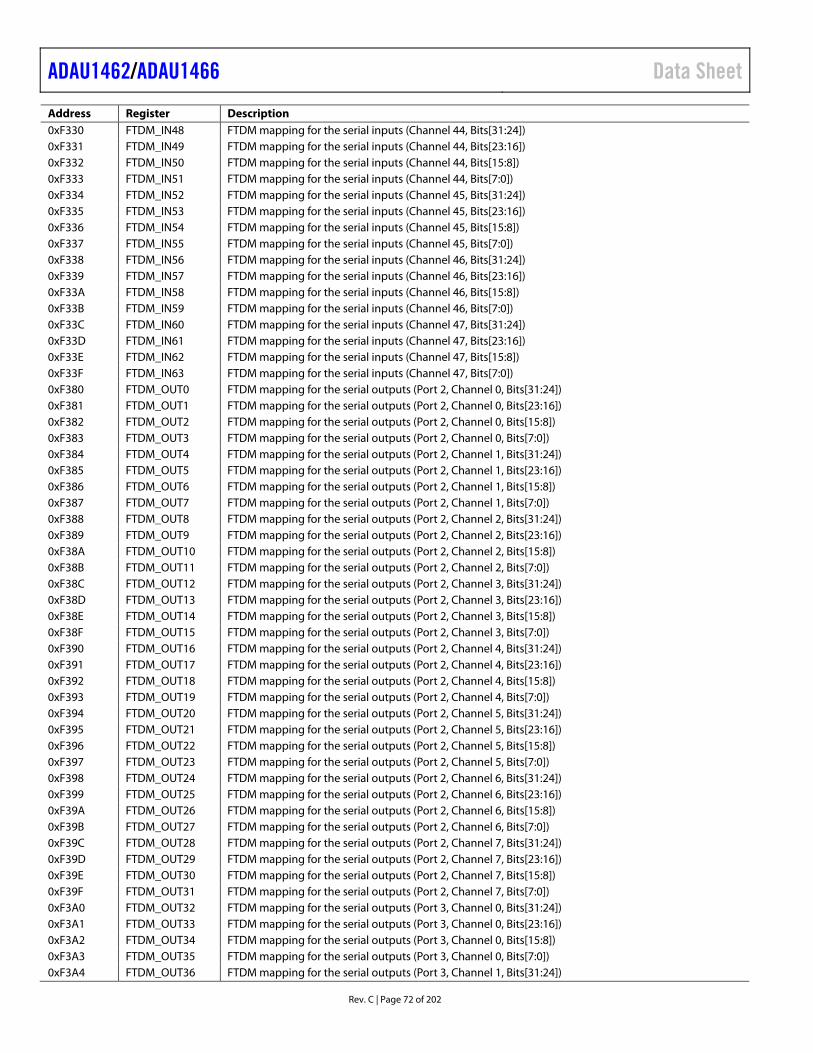
ADAU1462/ADAU1466 Data Sheet
Rev. C | Page 72 of 202
Address Register Description 0xF330 FTDM_IN48 FTDM mapping for the serial inputs (Channel 44, Bits[31:24]) 0xF331 FTDM_IN49 FTDM mapping for the serial inputs (Channel 44, Bits[23:16]) 0xF332 FTDM_IN50 FTDM mapping for the serial inputs (Channel 44, Bits[15:8]) 0xF333 FTDM_IN51 FTDM mapping for the serial inputs (Channel 44, Bits[7:0]) 0xF334 FTDM_IN52 FTDM mapping for the serial inputs (Channel 45, Bits[31:24]) 0xF335 FTDM_IN53 FTDM mapping for the serial inputs (Channel 45, Bits[23:16]) 0xF336 FTDM_IN54 FTDM mapping for the serial inputs (Channel 45, Bits[15:8]) 0xF337 FTDM_IN55 FTDM mapping for the serial inputs (Channel 45, Bits[7:0]) 0xF338 FTDM_IN56 FTDM mapping for the serial inputs (Channel 46, Bits[31:24]) 0xF339 FTDM_IN57 FTDM mapping for the serial inputs (Channel 46, Bits[23:16]) 0xF33A FTDM_IN58 FTDM mapping for the serial inputs (Channel 46, Bits[15:8]) 0xF33B FTDM_IN59 FTDM mapping for the serial inputs (Channel 46, Bits[7:0]) 0xF33C FTDM_IN60 FTDM mapping for the serial inputs (Channel 47, Bits[31:24]) 0xF33D FTDM_IN61 FTDM mapping for the serial inputs (Channel 47, Bits[23:16]) 0xF33E FTDM_IN62 FTDM mapping for the serial inputs (Channel 47, Bits[15:8]) 0xF33F FTDM_IN63 FTDM mapping for the serial inputs (Channel 47, Bits[7:0]) 0xF380 FTDM_OUT0 FTDM mapping for the serial outputs (Port 2, Channel 0, Bits[31:24]) 0xF381 FTDM_OUT1 FTDM mapping for the serial outputs (Port 2, Channel 0, Bits[23:16]) 0xF382 FTDM_OUT2 FTDM mapping for the serial outputs (Port 2, Channel 0, Bits[15:8]) 0xF383 FTDM_OUT3 FTDM mapping for the serial outputs (Port 2, Channel 0, Bits[7:0]) 0xF384 FTDM_OUT4 FTDM mapping for the serial outputs (Port 2, Channel 1, Bits[31:24]) 0xF385 FTDM_OUT5 FTDM mapping for the serial outputs (Port 2, Channel 1, Bits[23:16]) 0xF386 FTDM_OUT6 FTDM mapping for the serial outputs (Port 2, Channel 1, Bits[15:8]) 0xF387 FTDM_OUT7 FTDM mapping for the serial outputs (Port 2, Channel 1, Bits[7:0]) 0xF388 FTDM_OUT8 FTDM mapping for the serial outputs (Port 2, Channel 2, Bits[31:24]) 0xF389 FTDM_OUT9 FTDM mapping for the serial outputs (Port 2, Channel 2, Bits[23:16]) 0xF38A FTDM_OUT10 FTDM mapping for the serial outputs (Port 2, Channel 2, Bits[15:8]) 0xF38B FTDM_OUT11 FTDM mapping for the serial outputs (Port 2, Channel 2, Bits[7:0]) 0xF38C FTDM_OUT12 FTDM mapping for the serial outputs (Port 2, Channel 3, Bits[31:24]) 0xF38D FTDM_OUT13 FTDM mapping for the serial outputs (Port 2, Channel 3, Bits[23:16]) 0xF38E FTDM_OUT14 FTDM mapping for the serial outputs (Port 2, Channel 3, Bits[15:8]) 0xF38F FTDM_OUT15 FTDM mapping for the serial outputs (Port 2, Channel 3, Bits[7:0]) 0xF390 FTDM_OUT16 FTDM mapping for the serial outputs (Port 2, Channel 4, Bits[31:24]) 0xF391 FTDM_OUT17 FTDM mapping for the serial outputs (Port 2, Channel 4, Bits[23:16]) 0xF392 FTDM_OUT18 FTDM mapping for the serial outputs (Port 2, Channel 4, Bits[15:8]) 0xF393 FTDM_OUT19 FTDM mapping for the serial outputs (Port 2, Channel 4, Bits[7:0]) 0xF394 FTDM_OUT20 FTDM mapping for the serial outputs (Port 2, Channel 5, Bits[31:24]) 0xF395 FTDM_OUT21 FTDM mapping for the serial outputs (Port 2, Channel 5, Bits[23:16]) 0xF396 FTDM_OUT22 FTDM mapping for the serial outputs (Port 2, Channel 5, Bits[15:8]) 0xF397 FTDM_OUT23 FTDM mapping for the serial outputs (Port 2, Channel 5, Bits[7:0]) 0xF398 FTDM_OUT24 FTDM mapping for the serial outputs (Port 2, Channel 6, Bits[31:24]) 0xF399 FTDM_OUT25 FTDM mapping for the serial outputs (Port 2, Channel 6, Bits[23:16]) 0xF39A FTDM_OUT26 FTDM mapping for the serial outputs (Port 2, Channel 6, Bits[15:8]) 0xF39B FTDM_OUT27 FTDM mapping for the serial outputs (Port 2, Channel 6, Bits[7:0]) 0xF39C FTDM_OUT28 FTDM mapping for the serial outputs (Port 2, Channel 7, Bits[31:24]) 0xF39D FTDM_OUT29 FTDM mapping for the serial outputs (Port 2, Channel 7, Bits[23:16]) 0xF39E FTDM_OUT30 FTDM mapping for the serial outputs (Port 2, Channel 7, Bits[15:8]) 0xF39F FTDM_OUT31 FTDM mapping for the serial outputs (Port 2, Channel 7, Bits[7:0]) 0xF3A0 FTDM_OUT32 FTDM mapping for the serial outputs (Port 3, Channel 0, Bits[31:24]) 0xF3A1 FTDM_OUT33 FTDM mapping for the serial outputs (Port 3, Channel 0, Bits[23:16]) 0xF3A2 FTDM_OUT34 FTDM mapping for the serial outputs (Port 3, Channel 0, Bits[15:8]) 0xF3A3 FTDM_OUT35 FTDM mapping for the serial outputs (Port 3, Channel 0, Bits[7:0]) 0xF3A4 FTDM_OUT36 FTDM mapping for the serial outputs (Port 3, Channel 1, Bits[31:24])
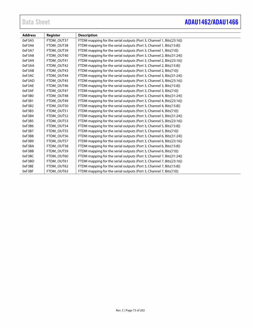
Data Sheet ADAU1462/ADAU1466
Rev. C | Page 73 of 202
Address Register Description 0xF3A5 FTDM_OUT37 FTDM mapping for the serial outputs (Port 3, Channel 1, Bits[23:16]) 0xF3A6 FTDM_OUT38 FTDM mapping for the serial outputs (Port 3, Channel 1, Bits[15:8]) 0xF3A7 FTDM_OUT39 FTDM mapping for the serial outputs (Port 3, Channel 1, Bits[7:0]) 0xF3A8 FTDM_OUT40 FTDM mapping for the serial outputs (Port 3, Channel 2, Bits[31:24]) 0xF3A9 FTDM_OUT41 FTDM mapping for the serial outputs (Port 3, Channel 2, Bits[23:16]) 0xF3AA FTDM_OUT42 FTDM mapping for the serial outputs (Port 3, Channel 2, Bits[15:8]) 0xF3AB FTDM_OUT43 FTDM mapping for the serial outputs (Port 3, Channel 2, Bits[7:0]) 0xF3AC FTDM_OUT44 FTDM mapping for the serial outputs (Port 3, Channel 3, Bits[31:24]) 0xF3AD FTDM_OUT45 FTDM mapping for the serial outputs (Port 3, Channel 3, Bits[23:16]) 0xF3AE FTDM_OUT46 FTDM mapping for the serial outputs (Port 3, Channel 3, Bits[15:8]) 0xF3AF FTDM_OUT47 FTDM mapping for the serial outputs (Port 3, Channel 3, Bits[7:0]) 0xF3B0 FTDM_OUT48 FTDM mapping for the serial outputs (Port 3, Channel 4, Bits[31:24]) 0xF3B1 FTDM_OUT49 FTDM mapping for the serial outputs (Port 3, Channel 4, Bits[23:16]) 0xF3B2 FTDM_OUT50 FTDM mapping for the serial outputs (Port 3, Channel 4, Bits[15:8]) 0xF3B3 FTDM_OUT51 FTDM mapping for the serial outputs (Port 3, Channel 4, Bits[7:0]) 0xF3B4 FTDM_OUT52 FTDM mapping for the serial outputs (Port 3, Channel 5, Bits[31:24]) 0xF3B5 FTDM_OUT53 FTDM mapping for the serial outputs (Port 3, Channel 5, Bits[23:16]) 0xF3B6 FTDM_OUT54 FTDM mapping for the serial outputs (Port 3, Channel 5, Bits[15:8]) 0xF3B7 FTDM_OUT55 FTDM mapping for the serial outputs (Port 3, Channel 5, Bits[7:0]) 0xF3B8 FTDM_OUT56 FTDM mapping for the serial outputs (Port 3, Channel 6, Bits[31:24]) 0xF3B9 FTDM_OUT57 FTDM mapping for the serial outputs (Port 3, Channel 6, Bits[23:16]) 0xF3BA FTDM_OUT58 FTDM mapping for the serial outputs (Port 3, Channel 6, Bits[15:8]) 0xF3BB FTDM_OUT59 FTDM mapping for the serial outputs (Port 3, Channel 6, Bits[7:0]) 0xF3BC FTDM_OUT60 FTDM mapping for the serial outputs (Port 3, Channel 7, Bits[31:24]) 0xF3BD FTDM_OUT61 FTDM mapping for the serial outputs (Port 3, Channel 7, Bits[23:16]) 0xF3BE FTDM_OUT62 FTDM mapping for the serial outputs (Port 3, Channel 7, Bits[15:8]) 0xF3BF FTDM_OUT63 FTDM mapping for the serial outputs (Port 3, Channel 7, Bits[7:0])
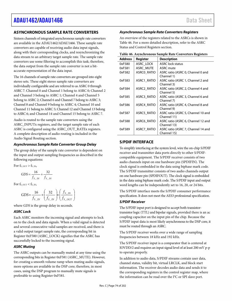
ADAU1462/ADAU1466 Data Sheet
Rev. C | Page 74 of 202
ASYNCHRONOUS SAMPLE RATE CONVERTERS Sixteen channels of integrated asynchronous sample rate converters are available in the ADAU1462/ADAU1466. These sample rate converters are capable of receiving audio data input signals, along with their corresponding clocks, and resynchronizing the data stream to an arbitrary target sample rate. The sample rate converters use some filtering to accomplish this task; therefore, the data output from the sample rate converter is not a bit-accurate representation of the data input.
The 16 channels of sample rate converters are grouped into eight stereo sets. These eight stereo sample rate converters are individually configurable and are referred to as ASRC 0 through ASRC 7. Channel 0 and Channel 1 belong to ASRC 0; Channel 2 and Channel 3 belong to ASRC 1; Channel 4 and Channel 5 belong to ASRC 2; Channel 6 and Channel 7 belong to ASRC 3; Channel 8 and Channel 9 belong to ASRC 4; Channel 10 and Channel 11 belong to ASRC 5; Channel 12 and Channel 13 belong to ASRC 6; and Channel 14 and Channel 15 belong to ASRC 7.
Audio is routed to the sample rate converters using the ASRC_INPUTx registers, and the target sample rate of each ASRC is configured using the ASRC_OUT_RATEx registers. A complete description of audio routing is included in the Audio Signal Routing section.
Asynchronous Sample Rate Converter Group Delay
The group delay of the sample rate converter is dependent on the input and output sampling frequencies as described in the following equations:
For fS_OUT > fS_IN,
INSINS ffGDS
__
3216
For fS_OUT < fS_IN,
OUTS
INS
INSINS ff
ffGDS
_
_
__
3216
where GDS is the group delay in seconds.
ASRC Lock
Each ASRC monitors the incoming signal and attempts to lock on to the clock and data signals. When a valid signal is detected and several consecutive valid samples are received, and there is a valid output target sample rate, the corresponding bit in Register 0xF580 (ASRC_LOCK) signifies that the ASRC has successfully locked to the incoming signal.
ASRC Muting
The ASRC outputs can be manually muted at any time using the corresponding bits in Register 0xF581 (ASRC_MUTE). However, for creating a smooth volume ramp when muting audio signals, more options are available in the DSP core; therefore, in most cases, using the DSP program to manually mute signals is preferable to using Register 0xF581.
Asynchronous Sample Rate Converters Registers
An overview of the registers related to the ASRCs is shown in Table 46. For a more detailed description, refer to the ASRC Status and Control Registers section.
Table 46. Asynchronous Sample Rate Converters Registers Address Register Description 0xF580 ASRC_LOCK ASRC lock status 0xF581 ASRC_MUTE ASRC mute 0xF582 ASRC0_RATIO ASRC ratio (ASRC 0, Channel 0 and
Channel 1) 0xF583 ASRC1_RATIO ASRC ratio (ASRC 1, Channel 2 and
Channel 3) 0xF584 ASRC2_RATIO ASRC ratio (ASRC 2, Channel 4 and
Channel 5) 0xF585 ASRC3_RATIO ASRC ratio (ASRC 3, Channel 6 and
Channel 7) 0xF586 ASRC4_RATIO ASRC ratio (ASRC 4, Channel 8 and
Channel 9) 0xF587 ASRC5_RATIO ASRC ratio (ASRC 5, Channel 10 and
Channel 11) 0xF588 ASRC6_RATIO ASRC ratio (ASRC 6, Channel 12 and
Channel 13) 0xF589 ASRC7_RATIO ASRC ratio (ASRC 7, Channel 14 and
Channel 15)
S/PDIF INTERFACE To simplify interfacing at the system level, wire the on-chip S/PDIF receiver and transmitter data ports directly to other S/PDIF-compatible equipment. The S/PDIF receiver consists of two audio channels input on one hardware pin (SPDIFIN). The clock signal is embedded in the data using biphase mark code. The S/PDIF transmitter consists of two audio channels output on one hardware pin (SPDIFOUT). The clock signal is embedded in the data using biphase mark code. The S/PDIF input and output word lengths can be independently set to 16, 20, or 24 bits.
The S/PDIF interface meets the S/PDIF consumer performance specification. It does not meet the AES3 professional specification.
S/PDIF Receiver
The S/PDIF input port is designed to accept both transistor-transistor logic (TTL) and bipolar signals, provided there is an ac coupling capacitor on the input pin of the chip. Because the S/PDIF input data is most likely asynchronous to the DSP core, it must be routed through an ASRC.
The S/PDIF receiver works over a wide range of sampling frequencies between 18 kHz and 192 kHz.
The S/PDIF receiver input is a comparator that is centered at IOVDD/2 and requires an input signal level of at least 200 mV p-p to operate properly.
In addition to audio data, S/PDIF streams contain user data, channel status, validity bit, virtual LRCLK, and block start information. The receiver decodes audio data and sends it to the corresponding registers in the control register map, where the information can be read over the I2C or SPI slave port.
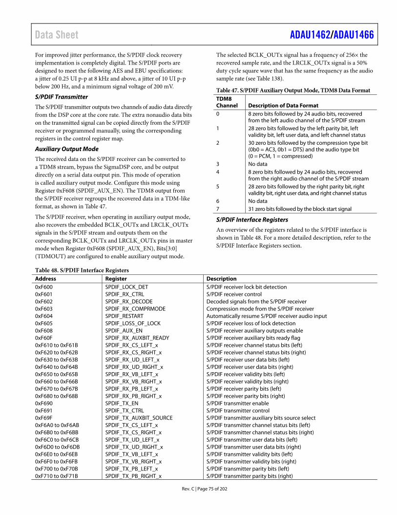
Data Sheet ADAU1462/ADAU1466
Rev. C | Page 75 of 202
For improved jitter performance, the S/PDIF clock recovery implementation is completely digital. The S/PDIF ports are designed to meet the following AES and EBU specifications: a jitter of 0.25 UI p-p at 8 kHz and above, a jitter of 10 UI p-p below 200 Hz, and a minimum signal voltage of 200 mV.
S/PDIF Transmitter
The S/PDIF transmitter outputs two channels of audio data directly from the DSP core at the core rate. The extra nonaudio data bits on the transmitted signal can be copied directly from the S/PDIF receiver or programmed manually, using the corresponding registers in the control register map.
Auxiliary Output Mode
The received data on the S/PDIF receiver can be converted to a TDM8 stream, bypass the SigmaDSP core, and be output directly on a serial data output pin. This mode of operation is called auxiliary output mode. Configure this mode using Register 0xF608 (SPDIF_AUX_EN). The TDM8 output from the S/PDIF receiver regroups the recovered data in a TDM-like format, as shown in Table 47.
The S/PDIF receiver, when operating in auxiliary output mode, also recovers the embedded BCLK_OUTx and LRCLK_OUTx signals in the S/PDIF stream and outputs them on the corresponding BCLK_OUTx and LRCLK_OUTx pins in master mode when Register 0xF608 (SPDIF_AUX_EN), Bits[3:0] (TDMOUT) are configured to enable auxiliary output mode.
The selected BCLK_OUTx signal has a frequency of 256× the recovered sample rate, and the LRCLK_OUTx signal is a 50% duty cycle square wave that has the same frequency as the audio sample rate (see Table 138).
Table 47. S/PDIF Auxiliary Output Mode, TDM8 Data Format TDM8 Channel Description of Data Format 0 8 zero bits followed by 24 audio bits, recovered
from the left audio channel of the S/PDIF stream 1 28 zero bits followed by the left parity bit, left
validity bit, left user data, and left channel status 2 30 zero bits followed by the compression type bit
(0b0 = AC3, 0b1 = DTS) and the audio type bit (0 = PCM, 1 = compressed)
3 No data 4 8 zero bits followed by 24 audio bits, recovered
from the right audio channel of the S/PDIF stream 5 28 zero bits followed by the right parity bit, right
validity bit, right user data, and right channel status 6 No data 7 31 zero bits followed by the block start signal
S/PDIF Interface Registers
An overview of the registers related to the S/PDIF interface is shown in Table 48. For a more detailed description, refer to the S/PDIF Interface Registers section.
Table 48. S/PDIF Interface Registers Address Register Description 0xF600 SPDIF_LOCK_DET S/PDIF receiver lock bit detection 0xF601 SPDIF_RX_CTRL S/PDIF receiver control 0xF602 SPDIF_RX_DECODE Decoded signals from the S/PDIF receiver 0xF603 SPDIF_RX_COMPRMODE Compression mode from the S/PDIF receiver 0xF604 SPDIF_RESTART Automatically resume S/PDIF receiver audio input 0xF605 SPDIF_LOSS_OF_LOCK S/PDIF receiver loss of lock detection 0xF608 SPDIF_AUX_EN S/PDIF receiver auxiliary outputs enable 0xF60F SPDIF_RX_AUXBIT_READY S/PDIF receiver auxiliary bits ready flag 0xF610 to 0xF61B SPDIF_RX_CS_LEFT_x S/PDIF receiver channel status bits (left) 0xF620 to 0xF62B SPDIF_RX_CS_RIGHT_x S/PDIF receiver channel status bits (right) 0xF630 to 0xF63B SPDIF_RX_UD_LEFT_x S/PDIF receiver user data bits (left) 0xF640 to 0xF64B SPDIF_RX_UD_RIGHT_x S/PDIF receiver user data bits (right) 0xF650 to 0xF65B SPDIF_RX_VB_LEFT_x S/PDIF receiver validity bits (left) 0xF660 to 0xF66B SPDIF_RX_VB_RIGHT_x S/PDIF receiver validity bits (right) 0xF670 to 0xF67B SPDIF_RX_PB_LEFT_x S/PDIF receiver parity bits (left) 0xF680 to 0xF68B SPDIF_RX_PB_RIGHT_x S/PDIF receiver parity bits (right) 0xF690 SPDIF_TX_EN S/PDIF transmitter enable 0xF691 SPDIF_TX_CTRL S/PDIF transmitter control 0xF69F SPDIF_TX_AUXBIT_SOURCE S/PDIF transmitter auxiliary bits source select 0xF6A0 to 0xF6AB SPDIF_TX_CS_LEFT_x S/PDIF transmitter channel status bits (left) 0xF6B0 to 0xF6BB SPDIF_TX_CS_RIGHT_x S/PDIF transmitter channel status bits (right) 0xF6C0 to 0xF6CB SPDIF_TX_UD_LEFT_x S/PDIF transmitter user data bits (left) 0xF6D0 to 0xF6DB SPDIF_TX_UD_RIGHT_x S/PDIF transmitter user data bits (right) 0xF6E0 to 0xF6EB SPDIF_TX_VB_LEFT_x S/PDIF transmitter validity bits (left) 0xF6F0 to 0xF6FB SPDIF_TX_VB_RIGHT_x S/PDIF transmitter validity bits (right) 0xF700 to 0xF70B SPDIF_TX_PB_LEFT_x S/PDIF transmitter parity bits (left) 0xF710 to 0xF71B SPDIF_TX_PB_RIGHT_x S/PDIF transmitter parity bits (right)
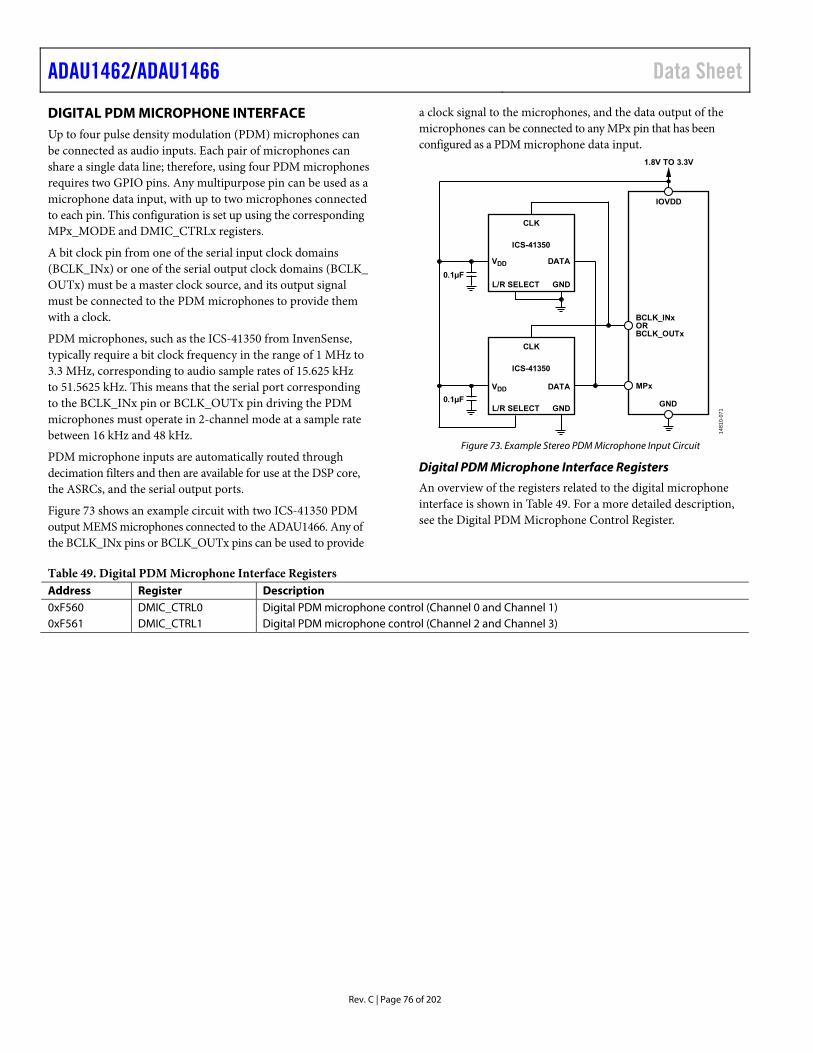
ADAU1462/ADAU1466 Data Sheet
Rev. C | Page 76 of 202
DIGITAL PDM MICROPHONE INTERFACE Up to four pulse density modulation (PDM) microphones can be connected as audio inputs. Each pair of microphones can share a single data line; therefore, using four PDM microphones requires two GPIO pins. Any multipurpose pin can be used as a microphone data input, with up to two microphones connected to each pin. This configuration is set up using the corresponding MPx_MODE and DMIC_CTRLx registers.
A bit clock pin from one of the serial input clock domains (BCLK_INx) or one of the serial output clock domains (BCLK_ OUTx) must be a master clock source, and its output signal must be connected to the PDM microphones to provide them with a clock.
PDM microphones, such as the ICS-41350 from InvenSense, typically require a bit clock frequency in the range of 1 MHz to 3.3 MHz, corresponding to audio sample rates of 15.625 kHz to 51.5625 kHz. This means that the serial port corresponding to the BCLK_INx pin or BCLK_OUTx pin driving the PDM microphones must operate in 2-channel mode at a sample rate between 16 kHz and 48 kHz.
PDM microphone inputs are automatically routed through decimation filters and then are available for use at the DSP core, the ASRCs, and the serial output ports.
Figure 73 shows an example circuit with two ICS-41350 PDM output MEMS microphones connected to the ADAU1466. Any of the BCLK_INx pins or BCLK_OUTx pins can be used to provide
a clock signal to the microphones, and the data output of the microphones can be connected to any MPx pin that has been configured as a PDM microphone data input.
BCLK_INxORBCLK_OUTx
GND
MPx
ICS-41350
IOVDD
GNDL/R SELECT
VDD
CLK
DATA
ICS-41350
GNDL/R SELECT
VDD
CLK
DATA
0.1µF
0.1µF
1.8V TO 3.3V
14
810
-07
1
Figure 73. Example Stereo PDM Microphone Input Circuit
Digital PDM Microphone Interface Registers
An overview of the registers related to the digital microphone interface is shown in Table 49. For a more detailed description, see the Digital PDM Microphone Control Register.
Table 49. Digital PDM Microphone Interface Registers Address Register Description 0xF560 DMIC_CTRL0 Digital PDM microphone control (Channel 0 and Channel 1) 0xF561 DMIC_CTRL1 Digital PDM microphone control (Channel 2 and Channel 3)
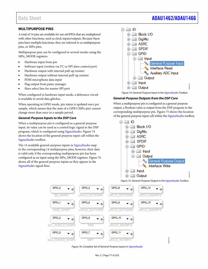
Data Sheet ADAU1462/ADAU1466
Rev. C | Page 77 of 202
MULTIPURPOSE PINS A total of 14 pins are available for use asGPIOs that are multiplexed with other functions, such as clock inputs/outputs. Because these pins have multiple functions, they are referred to as multipurpose pins, or MPx pins.
Multipurpose pins can be configured in several modes using the MPx_MODE registers:
Hardware input from pin Software input (written via I2C or SPI slave control port) Hardware output with internal pull-up resistor Hardware output without internal pull-up resistor PDM microphone data input Flag output from panic manager Slave select line for master SPI port
When configured in hardware input mode, a debounce circuit is available to avoid data glitches.
When operating in GPIO mode, pin status is updated once per sample, which means that the state of a GPIO (MPx pin) cannot change more than once in a sample period.
General-Purpose Inputs to the DSP Core
When a multipurpose pin is configured as a general-purpose input, its value can be used as a control logic signal in the DSP program, which is configured using SigmaStudio. Figure 74 shows the location of the general-purpose input cell within the SigmaStudio toolbox.
The 14 available general-purpose inputs in SigmaStudio map to the corresponding 14 multipurpose pins; however, their data is valid only if the corresponding multipurpose pin has been configured as an input using the MPx_MODE registers. Figure 76 shows all of the general-purpose inputs as they appear in the SigmaStudio signal flow.
1481
0-07
2
Figure 74. General-Purpose Input in the SigmaStudio Toolbox
General-Purpose Outputs from the DSP Core
When a multipurpose pin is configured as a general-purpose output, a Boolean value is output from the DSP program to the corresponding multipurpose pin. Figure 75 shows the location of the general-purpose input cell within the SigmaStudio toolbox.
1481
0-07
3
Figure 75. General-Purpose Output in the SigmaStudio Toolbox
14
81
0-0
74
Figure 76. Complete Set of General-Purpose Inputs in SigmaStudio
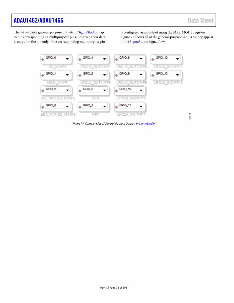
ADAU1462/ADAU1466 Data Sheet
Rev. C | Page 78 of 202
The 14 available general-purpose outputs in SigmaStudio map to the corresponding 14 multipurpose pins; however, their data is output to the pin only if the corresponding multipurpose pin
is configured as an output using the MPx_MODE registers. Figure 77 shows all of the general-purpose inputs as they appear in the SigmaStudio signal flow.
1481
0-07
5
Figure 77. Complete Set of General-Purpose Outputs in SigmaStudio
Data Sheet ADAU1462/ADAU1466
Rev. C | Page 79 of 202
Multipurpose Pin Registers
An overview of the registers related to GPIO is shown in Table 50. For a more detailed description, refer to the Multipurpose Pin Configuration Registers section.
Table 50. Multipurpose Pins Registers Address Register Description 0xF510 MP0_MODE Multipurpose pin mode (SS_M/MP0) 0xF511 MP1_MODE Multipurpose pin mode (MOSI_M/MP1) 0xF512 MP2_MODE Multipurpose pin mode (SCL_M/SCLK_M/MP2) 0xF513 MP3_MODE Multipurpose pin mode (SDA_M/MISO_M/MP3) 0xF514 MP4_MODE Multipurpose pin mode (LRCLK_OUT0/MP4) 0xF515 MP5_MODE Multipurpose pin mode (LRCLK_OUT1/MP5) 0xF516 MP6_MODE Multipurpose pin mode (MP6) 0xF517 MP7_MODE Multipurpose pin mode (MP7) 0xF518 MP8_MODE Multipurpose pin mode (LRCLK_OUT2/MP8) 0xF519 MP9_MODE Multipurpose pin mode (LRCLK_OUT3/MP9) 0xF51A MP10_MODE Multipurpose pin mode (LRCLK_IN0/MP10) 0xF51B MP11_MODE Multipurpose pin mode (LRCLK_IN1/MP11) 0xF51C MP12_MODE Multipurpose pin mode (LRCLK_IN2/MP12) 0xF51D MP13_MODE Multipurpose pin mode (LRCLK_IN3/MP13) 0xF520 MP0_WRITE Multipurpose pin write value (SS_M/MP0) 0xF521 MP1_WRITE Multipurpose pin write value (MOSI_M/MP1) 0xF522 MP2_WRITE Multipurpose pin write value (SCL_M/SCLK_M/MP2) 0xF523 MP3_WRITE Multipurpose pin write value (SDA_M/MISO_M/MP3) 0xF524 MP4_WRITE Multipurpose pin write value (LRCLK_OUT0/MP4) 0xF525 MP5_WRITE Multipurpose pin write value (LRCLK_OUT1/MP5) 0xF526 MP6_WRITE Multipurpose pin write value (MP6) 0xF527 MP7_WRITE Multipurpose pin write value (MP7) 0xF528 MP8_WRITE Multipurpose pin write value (LRCLK_OUT2/MP8) 0xF529 MP9_WRITE Multipurpose pin write value (LRCLK_OUT3/MP9) 0xF52A MP10_WRITE Multipurpose pin write value (LRCLK_IN0/MP10) 0xF52B MP11_WRITE Multipurpose pin write value (LRCLK_IN1/MP11) 0xF52C MP12_WRITE Multipurpose pin write value (LRCLK_IN2/MP12) 0xF52D MP13_WRITE Multipurpose pin write value (LRCLK_IN3/MP13) 0xF530 MP0_READ Multipurpose pin read value (SS_M/MP0) 0xF531 MP1_READ Multipurpose pin read value (MOSI_M/MP1) 0xF532 MP2_READ Multipurpose pin read value (SCL_M/SCLK_M/MP2) 0xF533 MP3_READ Multipurpose pin read value (SDA_M/MISO_M/MP3) 0xF534 MP4_READ Multipurpose pin read value (LRCLK_OUT0/MP4) 0xF535 MP5_READ Multipurpose pin read value (LRCLK_OUT1/MP5) 0xF536 MP6_READ Multipurpose pin read value (MP6) 0xF537 MP7_READ Multipurpose pin read value (MP7) 0xF538 MP8_READ Multipurpose pin read value (LRCLK_OUT2/MP8) 0xF539 MP9_READ Multipurpose pin read value (LRCLK_OUT3/MP9) 0xF53A MP10_READ Multipurpose pin read value (LRCLK_IN0/MP10) 0xF53B MP11_READ Multipurpose pin read value (LRCLK_IN1/MP11) 0xF53C MP12_READ Multipurpose pin read value (LRCLK_IN2/MP12) 0xF53D MP13_READ Multipurpose pin read value (LRCLK_IN3/MP13)
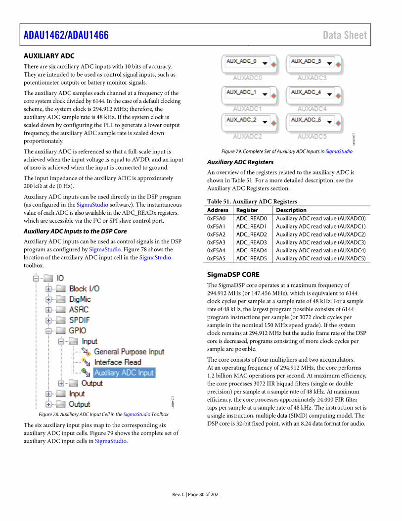
ADAU1462/ADAU1466 Data Sheet
Rev. C | Page 80 of 202
AUXILIARY ADC There are six auxiliary ADC inputs with 10 bits of accuracy. They are intended to be used as control signal inputs, such as potentiometer outputs or battery monitor signals.
The auxiliary ADC samples each channel at a frequency of the core system clock divided by 6144. In the case of a default clocking scheme, the system clock is 294.912 MHz; therefore, the auxiliary ADC sample rate is 48 kHz. If the system clock is scaled down by configuring the PLL to generate a lower output frequency, the auxiliary ADC sample rate is scaled down proportionately.
The auxiliary ADC is referenced so that a full-scale input is achieved when the input voltage is equal to AVDD, and an input of zero is achieved when the input is connected to ground.
The input impedance of the auxiliary ADC is approximately 200 kΩ at dc (0 Hz).
Auxiliary ADC inputs can be used directly in the DSP program (as configured in the SigmaStudio software). The instantaneous value of each ADC is also available in the ADC_READx registers, which are accessible via the I2C or SPI slave control port.
Auxiliary ADC Inputs to the DSP Core
Auxiliary ADC inputs can be used as control signals in the DSP program as configured by SigmaStudio. Figure 78 shows the location of the auxiliary ADC input cell in the SigmaStudio toolbox.
1481
0-0
76
Figure 78. Auxiliary ADC Input Cell in the SigmaStudio Toolbox
The six auxiliary input pins map to the corresponding six auxiliary ADC input cells. Figure 79 shows the complete set of auxiliary ADC input cells in SigmaStudio.
14
81
0-0
77
Figure 79. Complete Set of Auxiliary ADC Inputs in SigmaStudio
Auxiliary ADC Registers
An overview of the registers related to the auxiliary ADC is shown in Table 51. For a more detailed description, see the Auxiliary ADC Registers section.
Table 51. Auxiliary ADC Registers Address Register Description 0xF5A0 ADC_READ0 Auxiliary ADC read value (AUXADC0) 0xF5A1 ADC_READ1 Auxiliary ADC read value (AUXADC1) 0xF5A2 ADC_READ2 Auxiliary ADC read value (AUXADC2) 0xF5A3 ADC_READ3 Auxiliary ADC read value (AUXADC3) 0xF5A4 ADC_READ4 Auxiliary ADC read value (AUXADC4) 0xF5A5 ADC_READ5 Auxiliary ADC read value (AUXADC5)
SigmaDSP CORE The SigmaDSP core operates at a maximum frequency of 294.912 MHz (or 147.456 MHz), which is equivalent to 6144 clock cycles per sample at a sample rate of 48 kHz. For a sample rate of 48 kHz, the largest program possible consists of 6144 program instructions per sample (or 3072 clock cycles per sample in the nominal 150 MHz speed grade). If the system clock remains at 294.912 MHz but the audio frame rate of the DSP core is decreased, programs consisting of more clock cycles per sample are possible.
The core consists of four multipliers and two accumulators. At an operating frequency of 294.912 MHz, the core performs 1.2 billion MAC operations per second. At maximum efficiency, the core processes 3072 IIR biquad filters (single or double precision) per sample at a sample rate of 48 kHz. At maximum efficiency, the core processes approximately 24,000 FIR filter taps per sample at a sample rate of 48 kHz. The instruction set is a single instruction, multiple data (SIMD) computing model. The DSP core is 32-bit fixed point, with an 8.24 data format for audio.
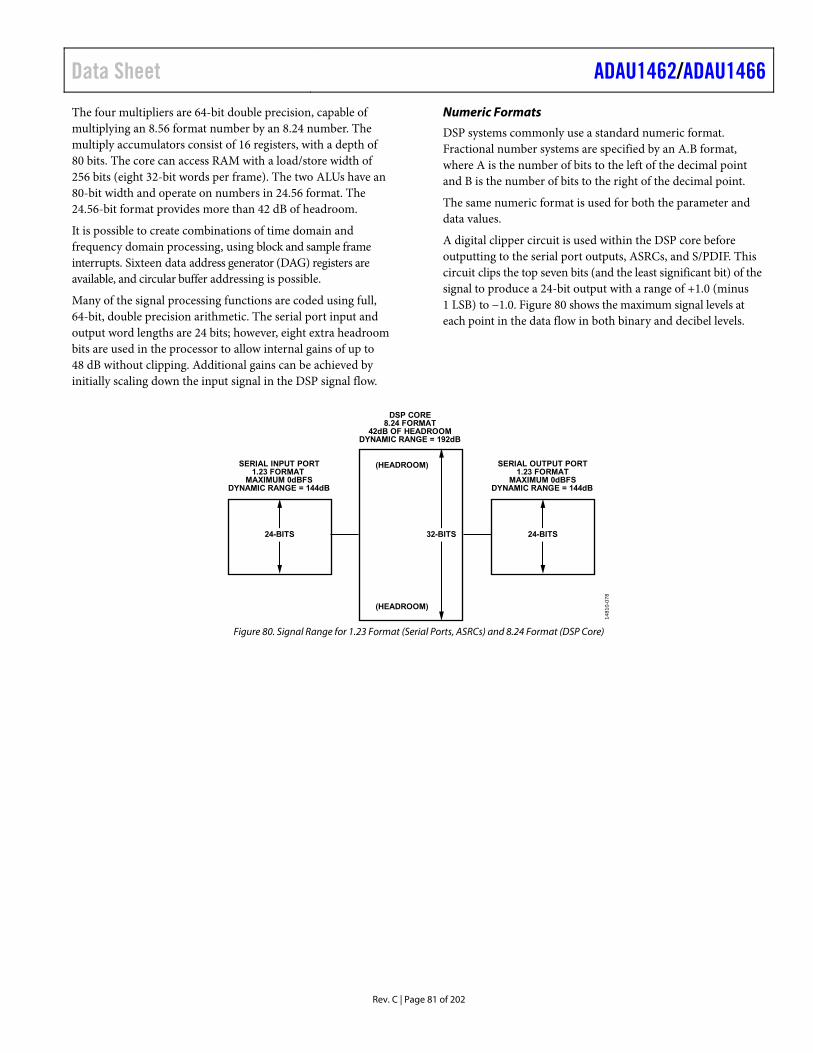
Data Sheet ADAU1462/ADAU1466
Rev. C | Page 81 of 202
The four multipliers are 64-bit double precision, capable of multiplying an 8.56 format number by an 8.24 number. The multiply accumulators consist of 16 registers, with a depth of 80 bits. The core can access RAM with a load/store width of 256 bits (eight 32-bit words per frame). The two ALUs have an 80-bit width and operate on numbers in 24.56 format. The 24.56-bit format provides more than 42 dB of headroom.
It is possible to create combinations of time domain and frequency domain processing, using block and sample frame interrupts. Sixteen data address generator (DAG) registers are available, and circular buffer addressing is possible.
Many of the signal processing functions are coded using full, 64-bit, double precision arithmetic. The serial port input and output word lengths are 24 bits; however, eight extra headroom bits are used in the processor to allow internal gains of up to 48 dB without clipping. Additional gains can be achieved by initially scaling down the input signal in the DSP signal flow.
Numeric Formats
DSP systems commonly use a standard numeric format. Fractional number systems are specified by an A.B format, where A is the number of bits to the left of the decimal point and B is the number of bits to the right of the decimal point.
The same numeric format is used for both the parameter and data values.
A digital clipper circuit is used within the DSP core before outputting to the serial port outputs, ASRCs, and S/PDIF. This circuit clips the top seven bits (and the least significant bit) of the signal to produce a 24-bit output with a range of +1.0 (minus 1 LSB) to −1.0. Figure 80 shows the maximum signal levels at each point in the data flow in both binary and decibel levels.
SERIAL INPUT PORT1.23 FORMAT
MAXIMUM 0dBFSDYNAMIC RANGE = 144dB
DSP CORE8.24 FORMAT
42dB OF HEADROOMDYNAMIC RANGE = 192dB
SERIAL OUTPUT PORT1.23 FORMAT
MAXIMUM 0dBFSDYNAMIC RANGE = 144dB
24-BITS 24-BITS32-BITS
(HEADROOM)
(HEADROOM)1
48
10
-07
8
Figure 80. Signal Range for 1.23 Format (Serial Ports, ASRCs) and 8.24 Format (DSP Core)
ADAU1462/ADAU1466 Data Sheet
Rev. C | Page 82 of 202
Numerical Format: 8.24
The linear range is −128.0 to (+128.0 − 1 LSB). The dynamic range (ratio of the largest possible signal level to the smallest possible nonzero signal level) is 192 dB.
The following are examples of this numerical format:
0b 1000 0000 0000 0000 0000 0000 0000 0000 = 0x80000000 = −128.0
0b 1110 0000 0000 0000 0000 0000 0000 0000 = 0xE0000000 = −32.0
0b 1111 1000 0000 0000 0000 0000 0000 0000 = 0xF8000000 = −8.0
0b 1111 1110 0000 0000 0000 0000 0000 0000 = 0xFE000000 = −2
0b 1111 1111 0000 0000 0000 0000 0000 0000 = 0xFF000000 = −1
0b 1111 1111 1000 0000 0000 0000 0000 0000 = 0xFF800000 = −0.5
0b 1111 1111 1110 0110 0110 0110 0110 0110 = 0xFFE66666 = −0.1
0b 1111 1111 1111 1111 1111 1111 1111 1111 = 0xFFFFFFFF = −0.00000005 (1 LSB below 0.0)
0b 0000 0000 0000 0000 0000 0000 0000 0000 = 0x00000000 = 0.0
0b 0000 0000 0000 0000 0000 0000 0000 0001 = 0x00000001 = 0.00000005 (1 LSB above 0.0)
0b 0000 0000 0001 1001 1001 1001 1001 1001 = 0x00199999 = 0.1
0b 0000 0000 0100 0000 0000 0000 0000 0000 = 0x00400000 = 0.25
0b 0000 0000 1000 0000 0000 0000 0000 0000 = 0x00800000 = 0.5
0b 0000 0001 0000 0000 0000 0000 0000 0000 = 0x01000000 = 1.0
0b 0000 0010 0000 0000 0000 0000 0000 0000 = 0x02000000 = 2.0
0b 0111 1111 1111 1111 1111 1111 1111 1111 = 0x7FFFFFFF = 127.99999994 (1 LSB below 128.0)
Data Sheet ADAU1462/ADAU1466
Rev. C | Page 83 of 202
Numerical Format: 32.0
The 32.0 format is used for logic signals in the DSP program flow that are integers. The linear range is −2,147,483,648 to +2,147,483,647. The dynamic range (ratio of the largest possible signal level to the smallest possible nonzero signal level) is 192 dB.
The following are examples of this numerical format:
0b 1000 0000 0000 0000 0000 0000 0000 0000 = 0x80000000 = −2147483648
0b 1000 0000 0000 0000 0000 0000 0000 0001 = 0x80000001 = −2147483647
0b 1000 0000 0000 0000 0000 0000 0000 0010 = 0x80000002 = −2147483646
0b 1100 0000 0000 0000 0000 0000 0000 0000 = 0xC0000000 = −1073741824
0b 1110 0000 0000 0000 0000 0000 0000 0000 = 0xE0000000 = −536870912
0b 1111 1111 1111 1111 1111 1111 1111 1100 = 0xFFFFFFFC = −4
0b 1111 1111 1111 1111 1111 1111 1111 1110 = 0xFFFFFFFE = −2
0b 1111 1111 1111 1111 1111 1111 1111 1111 = 0xFFFFFFFF = −1
0b 0000 0000 0000 0000 0000 0000 0000 0000 = 0x00000000 = 0
0b 0000 0000 0000 0000 0000 0000 0000 0001 = 0x00000001 = 1
0b 0000 0000 0000 0000 0000 0000 0000 0010 = 0x00000002 = 2
0b 0000 0000 0000 0000 0000 0000 0000 0011 = 0x00000003 = 3
0b 0000 0000 0000 0000 0000 0000 0000 0100 = 0x00000004 = 4
0b 0111 1111 1111 1111 1111 1111 1111 1110 = 0x7FFFFFFE = 2147483646
0b 0111 1111 1111 1111 1111 1111 1111 1111 = 0x7FFFFFFF = 2147483647
ADAU1462/ADAU1466 Data Sheet
Rev. C | Page 84 of 202
Hardware Accelerators
The core includes accelerators like division, square root, barrel shifters, Base 2 logarithm, Base 2 exponential, slew, and a pseudorandom number generator. These hardware accelerators reduce the number of instructions required for complex audio processing algorithms.
The division accelerator enables efficient processing for audio algorithms like compression and limiting. The square root accelerator enables efficient processing for audio algorithms such as loudness, rms envelopes, and filter coefficient calculations. The logarithm and exponent accelerators enable efficient processing for audio algorithms involving decibel conversion. The slew accelerators provide click free updates of parameters that must change slowly over time, allowing audio processing algorithms such as mixers, crossfaders, dynamic filters, and dynamic volume controls. The pseudorandom number generator can efficiently produce white noise, pink noise, and dither.
Programming the SigmaDSP Core
The SigmaDSP is programmable via the SigmaStudio graphical development tools.
When the SigmaDSP core is running a program and the user needs to reprogram the program and data memories during operation of the device, the core must be stopped while the memory is being updated to avoid undesired noises on the DSP outputs.
The following sequence of steps is appropriate for programming the memories at boot time, or reprogramming the memories during operation:
1. Enable soft reset (Register 0xF890 (SOFT_RESET), Bit 0 (SOFT_RESET) = 0b0), then disable soft reset (Register 0xF890 (SOFT_RESET), Bit 0 (SOFT_RESET) = 0b1).
2. If the DSP is in the process of executing a program, wait for the current sample or block to finish processing. For programs with no block processing elements in the signal flow, use the length of one sample. For example, at a sample rate of 48 kHz, one sample is 1/48000 sec, or 20.83 μs. For programs with block processing elements in the signal flow, use the length of one block. For example, at a sample rate of 48 kHz, with a block size of 256 samples, one block is 256/48,000 sec, or 53.3 ms.
3. After waiting the appropriate amount of time, as defined in the previous step, download the new program and data memory contents to the corresponding memory locations using the I2C/SPI slave control port.
4. Start the DSP core (Register 0xF402 (START_CORE), Bit 0 (START_CORE) = 0b1).
5. Wait at least two audio samples for the DSP initialization to execute. For example, at a sample rate of 48 kHz, two samples are equal to 2/48,000 sec, or 41.66 μs.
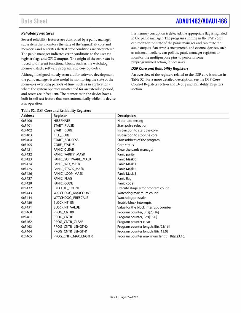
Data Sheet ADAU1462/ADAU1466
Rev. C | Page 85 of 202
Reliability Features
Several reliability features are controlled by a panic manager subsystem that monitors the state of the SigmaDSP core and memories and generates alerts if error conditions are encountered. The panic manager indicates error conditions to the user via register flags and GPIO outputs. The origin of the error can be traced to different functional blocks such as the watchdog, memory, stack, software program, and core op codes.
Although designed mostly as an aid for software development, the panic manager is also useful in monitoring the state of the memories over long periods of time, such as in applications where the system operates unattended for an extended period, and resets are infrequent. The memories in the device have a built in self test feature that runs automatically while the device is in operation.
If a memory corruption is detected, the appropriate flag is signaled in the panic manager. The program running in the DSP core can monitor the state of the panic manager and can mute the audio outputs if an error is encountered, and external devices, such as microcontrollers, can poll the panic manager registers or monitor the multipurpose pins to perform some preprogrammed action, if necessary.
DSP Core and Reliability Registers
An overview of the registers related to the DSP core is shown in Table 52. For a more detailed description, see the DSP Core Control Registers section and Debug and Reliability Registers section.
Table 52. DSP Core and Reliability Registers Address Register Description 0xF400 HIBERNATE Hibernate setting 0xF401 START_PULSE Start pulse selection 0xF402 START_CORE Instruction to start the core 0xF403 KILL_CORE Instruction to stop the core 0xF404 START_ADDRESS Start address of the program 0xF405 CORE_STATUS Core status 0xF421 PANIC_CLEAR Clear the panic manager 0xF422 PANIC_PARITY_MASK Panic parity 0xF423 PANIC_SOFTWARE_MASK Panic Mask 0 0xF424 PANIC_WD_MASK Panic Mask 1 0xF425 PANIC_STACK_MASK Panic Mask 2 0xF426 PANIC_LOOP_MASK Panic Mask 3 0xF427 PANIC_FLAG Panic flag 0xF428 PANIC_CODE Panic code 0xF432 EXECUTE_COUNT Execute stage error program count 0xF443 WATCHDOG_MAXCOUNT Watchdog maximum count 0xF444 WATCHDOG_PRESCALE Watchdog prescale 0xF450 BLOCKINT_EN Enable block interrupts 0xF451 BLOCKINT_VALUE Value for the block interrupt counter 0xF460 PROG_CNTR0 Program counter, Bits[23:16] 0xF461 PROG_CNTR1 Program counter, Bits[15:0] 0xF462 PROG_CNTR_CLEAR Program counter clear 0xF463 PROG_CNTR_LENGTH0 Program counter length, Bits[23:16] 0xF464 PROG_CNTR_LENGTH1 Program counter length, Bits[15:0] 0xF465 PROG_CNTR_MAXLENGTH0 Program counter maximum length, Bits[23:16]
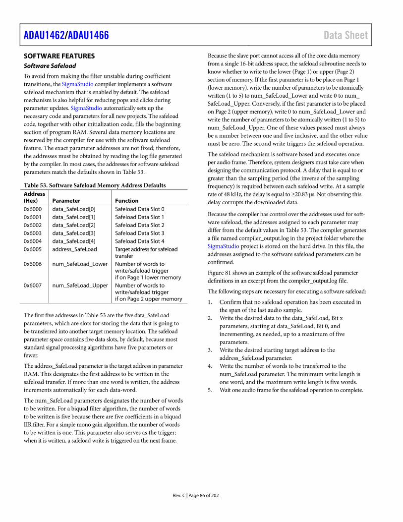
ADAU1462/ADAU1466 Data Sheet
Rev. C | Page 86 of 202
SOFTWARE FEATURES Software Safeload
To avoid from making the filter unstable during coefficient transitions, the SigmaStudio compiler implements a software safeload mechanism that is enabled by default. The safeload mechanism is also helpful for reducing pops and clicks during parameter updates. SigmaStudio automatically sets up the necessary code and parameters for all new projects. The safeload code, together with other initialization code, fills the beginning section of program RAM. Several data memory locations are reserved by the compiler for use with the software safeload feature. The exact parameter addresses are not fixed; therefore, the addresses must be obtained by reading the log file generated by the compiler. In most cases, the addresses for software safeload parameters match the defaults shown in Table 53.
Table 53. Software Safeload Memory Address Defaults Address (Hex) Parameter Function 0x6000 data_SafeLoad[0] Safeload Data Slot 0 0x6001 data_SafeLoad[1] Safeload Data Slot 1 0x6002 data_SafeLoad[2] Safeload Data Slot 2 0x6003 data_SafeLoad[3] Safeload Data Slot 3 0x6004 data_SafeLoad[4] Safeload Data Slot 4 0x6005 address_SafeLoad Target address for safeload
transfer 0x6006 num_SafeLoad_Lower Number of words to
write/safeload trigger if on Page 1 lower memory
0x6007 num_SafeLoad_Upper Number of words to write/safeload trigger if on Page 2 upper memory
The first five addresses in Table 53 are the five data_SafeLoad parameters, which are slots for storing the data that is going to be transferred into another target memory location. The safeload parameter space contains five data slots, by default, because most standard signal processing algorithms have five parameters or fewer.
The address_SafeLoad parameter is the target address in parameter RAM. This designates the first address to be written in the safeload transfer. If more than one word is written, the address increments automatically for each data-word.
The num_SafeLoad parameters designates the number of words to be written. For a biquad filter algorithm, the number of words to be written is five because there are five coefficients in a biquad IIR filter. For a simple mono gain algorithm, the number of words to be written is one. This parameter also serves as the trigger; when it is written, a safeload write is triggered on the next frame.
Because the slave port cannot access all of the core data memory from a single 16-bit address space, the safeload subroutine needs to know whether to write to the lower (Page 1) or upper (Page 2) section of memory. If the first parameter is to be place on Page 1 (lower memory), write the number of parameters to be atomically written (1 to 5) to num_SafeLoad_Lower and write 0 to num_ SafeLoad_Upper. Conversely, if the first parameter is to be placed on Page 2 (upper memory), write 0 to num_SafeLoad_Lower and write the number of parameters to be atomically written (1 to 5) to num_SafeLoad_Upper. One of these values passed must always be a number between one and five inclusive, and the other value must be zero. The second write triggers the safeload operation.
The safeload mechanism is software based and executes once per audio frame. Therefore, system designers must take care when designing the communication protocol. A delay that is equal to or greater than the sampling period (the inverse of the sampling frequency) is required between each safeload write. At a sample rate of 48 kHz, the delay is equal to ≥20.83 μs. Not observing this delay corrupts the downloaded data.
Because the compiler has control over the addresses used for soft-ware safeload, the addresses assigned to each parameter may differ from the default values in Table 53. The compiler generates a file named compiler_output.log in the project folder where the SigmaStudio project is stored on the hard drive. In this file, the addresses assigned to the software safeload parameters can be confirmed.
Figure 81 shows an example of the software safeload parameter definitions in an excerpt from the compiler_output.log file.
The following steps are necessary for executing a software safeload:
1. Confirm that no safeload operation has been executed in the span of the last audio sample.
2. Write the desired data to the data_SafeLoad, Bit x parameters, starting at data_SafeLoad, Bit 0, and incrementing, as needed, up to a maximum of five parameters.
3. Write the desired starting target address to the address_SafeLoad parameter.
4. Write the number of words to be transferred to the num_SafeLoad parameter. The minimum write length is one word, and the maximum write length is five words.
5. Wait one audio frame for the safeload operation to complete.
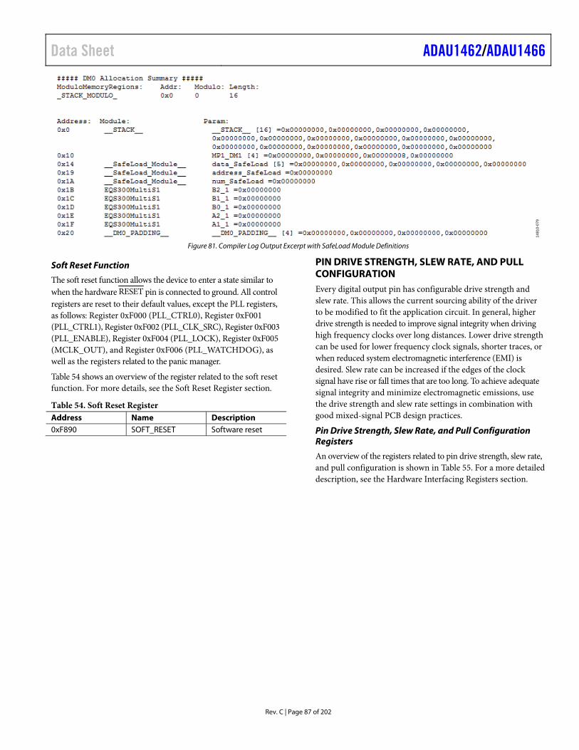
Data Sheet ADAU1462/ADAU1466
Rev. C | Page 87 of 202
1481
0-0
79
Figure 81. Compiler Log Output Excerpt with SafeLoad Module Definitions
Soft Reset Function
The soft reset function allows the device to enter a state similar to when the hardware RESET pin is connected to ground. All control registers are reset to their default values, except the PLL registers, as follows: Register 0xF000 (PLL_CTRL0), Register 0xF001 (PLL_CTRL1), Register 0xF002 (PLL_CLK_SRC), Register 0xF003 (PLL_ENABLE), Register 0xF004 (PLL_LOCK), Register 0xF005 (MCLK_OUT), and Register 0xF006 (PLL_WATCHDOG), as well as the registers related to the panic manager.
Table 54 shows an overview of the register related to the soft reset function. For more details, see the Soft Reset Register section.
Table 54. Soft Reset Register Address Name Description 0xF890 SOFT_RESET Software reset
PIN DRIVE STRENGTH, SLEW RATE, AND PULL CONFIGURATION Every digital output pin has configurable drive strength and slew rate. This allows the current sourcing ability of the driver to be modified to fit the application circuit. In general, higher drive strength is needed to improve signal integrity when driving high frequency clocks over long distances. Lower drive strength can be used for lower frequency clock signals, shorter traces, or when reduced system electromagnetic interference (EMI) is desired. Slew rate can be increased if the edges of the clock signal have rise or fall times that are too long. To achieve adequate signal integrity and minimize electromagnetic emissions, use the drive strength and slew rate settings in combination with good mixed-signal PCB design practices.
Pin Drive Strength, Slew Rate, and Pull Configuration Registers
An overview of the registers related to pin drive strength, slew rate, and pull configuration is shown in Table 55. For a more detailed description, see the Hardware Interfacing Registers section.
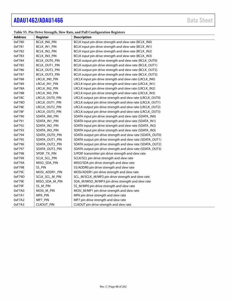
ADAU1462/ADAU1466 Data Sheet
Rev. C | Page 88 of 202
Table 55. Pin Drive Strength, Slew Rate, and Pull Configuration Registers Address Register Description 0xF780 BCLK_IN0_PIN BCLK input pin drive strength and slew rate (BCLK_IN0) 0xF781 BCLK_IN1_PIN BCLK input pin drive strength and slew rate (BCLK_IN1) 0xF782 BCLK_IN2_PIN BCLK input pin drive strength and slew rate (BCLK_IN2) 0xF783 BCLK_IN3_PIN BCLK input pin drive strength and slew rate (BCLK_IN3) 0xF784 BCLK_OUT0_PIN BCLK output pin drive strength and slew rate (BCLK_OUT0) 0xF785 BCLK_OUT1_PIN BCLK output pin drive strength and slew rate (BCLK_OUT1) 0xF786 BCLK_OUT2_PIN BCLK output pin drive strength and slew rate (BCLK_OUT2) 0xF787 BCLK_OUT3_PIN BCLK output pin drive strength and slew rate (BCLK_OUT3) 0xF788 LRCLK_IN0_PIN LRCLK input pin drive strength and slew rate (LRCLK_IN0) 0xF789 LRCLK_IN1_PIN LRCLK input pin drive strength and slew rate (LRCLK_IN1) 0xF78A LRCLK_IN2_PIN LRCLK input pin drive strength and slew rate (LRCLK_IN2) 0xF78B LRCLK_IN3_PIN LRCLK input pin drive strength and slew rate (LRCLK_IN3) 0xF78C LRCLK_OUT0_PIN LRCLK output pin drive strength and slew rate (LRCLK_OUT0) 0xF78D LRCLK_OUT1_PIN LRCLK output pin drive strength and slew rate (LRCLK_OUT1) 0xF78E LRCLK_OUT2_PIN LRCLK output pin drive strength and slew rate (LRCLK_OUT2) 0xF78F LRCLK_OUT3_PIN LRCLK output pin drive strength and slew rate (LRCLK_OUT3) 0xF790 SDATA_IN0_PIN SDATA input pin drive strength and slew rate (SDATA_IN0) 0xF791 SDATA_IN1_PIN SDATA input pin drive strength and slew rate (SDATA_IN1) 0xF792 SDATA_IN2_PIN SDATA input pin drive strength and slew rate (SDATA_IN2) 0xF793 SDATA_IN3_PIN SDATA input pin drive strength and slew rate (SDATA_IN3) 0xF794 SDATA_OUT0_PIN SDATA output pin drive strength and slew rate (SDATA_OUT0) 0xF795 SDATA_OUT1_PIN SDATA output pin drive strength and slew rate (SDATA_OUT1) 0xF796 SDATA_OUT2_PIN SDATA output pin drive strength and slew rate (SDATA_OUT2) 0xF797 SDATA_OUT3_PIN SDATA output pin drive strength and slew rate (SDATA_OUT3) 0xF798 SPDIF_TX_PIN S/PDIF transmitter pin drive strength and slew rate 0xF799 SCLK_SCL_PIN SCLK/SCL pin drive strength and slew rate 0xF79A MISO_SDA_PIN MISO/SDA pin drive strength and slew rate 0xF79B SS_PIN SS/ADDR0 pin drive strength and slew rate 0xF79C MOSI_ADDR1_PIN MOSI/ADDR1 pin drive strength and slew rate 0xF79D SCLK_SCL_M_PIN SCL_M/SCLK_M/MP2 pin drive strength and slew rate 0xF79E MISO_SDA_M_PIN SDA_M/MISO_M/MP3 pin drive strength and slew rate 0xF79F SS_M_PIN SS_M/MP0 pin drive strength and slew rate 0xF7A0 MOSI_M_PIN MOSI_M/MP1 pin drive strength and slew rate 0xF7A1 MP6_PIN MP6 pin drive strength and slew rate 0xF7A2 MP7_PIN MP7 pin drive strength and slew rate 0xF7A3 CLKOUT_PIN CLKOUT pin drive strength and slew rate
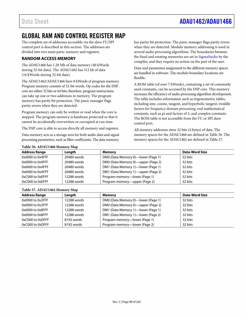
Data Sheet ADAU1462/ADAU1466
Rev. C | Page 89 of 202
GLOBAL RAM AND CONTROL REGISTER MAP The complete set of addresses accessible via the slave I2C/SPI control port is described in this section. The addresses are divided into two main parts: memory and registers.
RANDOM ACCESS MEMORY The ADAU1466 has 1.28 Mb of data memory (40 kWords storing 32-bit data). The ADAU1462 has 512 kb of data (16 kWords storing 32-bit data).
The ADAU1462/ADAU1466 have 8 kWords of program memory. Program memory consists of 32-bit words. Op codes for the DSP core are either 32 bits or 64 bits; therefore, program instructions can take up one or two addresses in memory. The program memory has parity bit protection. The panic manager flags parity errors when they are detected.
Program memory can only be written or read when the core is stopped. The program memory is hardware protected so that it cannot be accidentally overwritten or corrupted at run time.
The DSP core is able to access directly all memory and registers.
Data memory acts as a storage area for both audio data and signal processing parameters, such as filter coefficients. The data memory
has parity bit protection. The panic manager flags parity errors when they are detected. Modulo memory addressing is used in several audio processing algorithms. The boundaries between the fixed and rotating memories are set in SigmaStudio by the compiler, and they require no action on the part of the user.
Data and parameters assignment to the different memory spaces are handled in software. The modulo boundary locations are flexible.
A ROM table (of over 7 kWords), containing a set of commonly used constants, can be accessed by the DSP core. This memory increases the efficiency of audio processing algorithm development. The table includes information such as trigonometric tables, including sine, cosine, tangent, and hyperbolic tangent, twiddle factors for frequency domain processing, real mathematical constants, such as pi and factors of 2, and complex constants. The ROM table is not accessible from the I2C or SPI slave control port.
All memory addresses store 32 bits (4 bytes) of data. The memory spaces for the ADAU1466 are defined in Table 56. The memory spaces for the ADAU1462 are defined in Table 57.
Table 56. ADAU1466 Memory Map Address Range Length Memory Data-Word Size 0x0000 to 0x4FFF 20480 words DM0 (Data Memory 0)—lower (Page 1) 32 bits 0x0000 to 0x4FFF 20480 words DM0 (Data Memory 0)—upper (Page 2) 32 bits 0x6000 to 0xAFFF 20480 words DM1 (Data Memory 1)—lower (Page 1) 32 bits 0x6000 to 0xAFFF 20480 words DM1 (Data Memory 1)—upper (Page 2) 32 bits 0xC000 to 0xEFFF 12288 words Program memory—lower (Page 1) 32 bits 0xC000 to 0xEFFF 12288 words Program memory—upper (Page 2) 32 bits
Table 57. ADAU1462 Memory Map Address Range Length Memory Data-Word Size 0x0000 to 0x2FFF 12288 words DM0 (Data Memory 0)—lower (Page 1) 32 bits 0x0000 to 0x2FFF 12288 words DM0 (Data Memory 0)—upper (Page 2) 32 bits 0x6000 to 0x8FFF 12288 words DM1 (Data Memory 1)—lower (Page 1) 32 bits 0x6000 to 0x8FFF 12288 words DM1 (Data Memory 1)—lower (Page 2) 32 bits 0xC000 to 0xDFFF 8192 words Program memory—lower (Page 1) 32 bits 0xC000 to 0xDFFF 8192 words Program memory—lower (Page 2) 32 bits
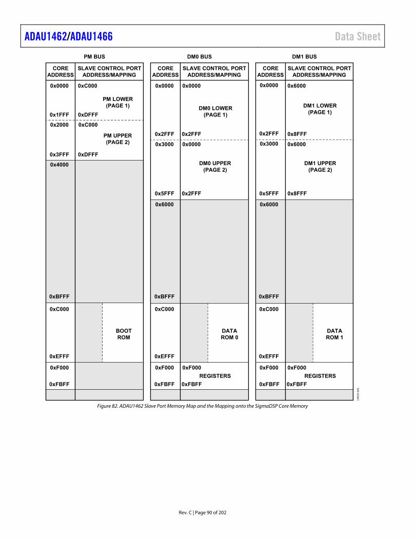
ADAU1462/ADAU1466 Data Sheet
Rev. C | Page 90 of 202
148
10-1
81
DM0 BUS
DM0 LOWER(PAGE 1)
DM0 UPPER(PAGE 2)
REGISTERS
DATAROM 0
0xC000
0xEFFF
0xF000
0xFBFF
0xBFFF
0x6000
0x8FFF
COREADDRESS
SLAVE CONTROL PORTADDRESS/MAPPING
DM1 BUS
0x5FFF
0x6000
DM1 LOWER(PAGE 1)
DM1 UPPER(PAGE 2)
REGISTERS
DATAROM 1
0xC000
0xEFFF
0xF000
0xFBFF
0xF000
0xFBFF
0xF000
0xFBFF
0xBFFF
0x6000
0x8FFF
COREADDRESS
SLAVE CONTROL PORTADDRESS/MAPPING
PM BUS
0x0000 0xC000
0x3FFF
0x4000
0xDFFF
COREADDRESS
SLAVE CONTROL PORTADDRESS/MAPPING
0x1FFF
0xC000
PM LOWER(PAGE 1)
PM UPPER(PAGE 2)
0xDFFF
0x2000
BOOTROM
0xC000
0xF000
0xFBFF
0xBFFF
0xEFFF
0x0000
0x2FFF
0x0000
0x0000
0x2FFF
0x3000
0x0000
0x2FFF
0x3000
0x5FFF
0x6000
0x2FFF
Figure 82. ADAU1462 Slave Port Memory Map and the Mapping onto the SigmaDSP Core Memory
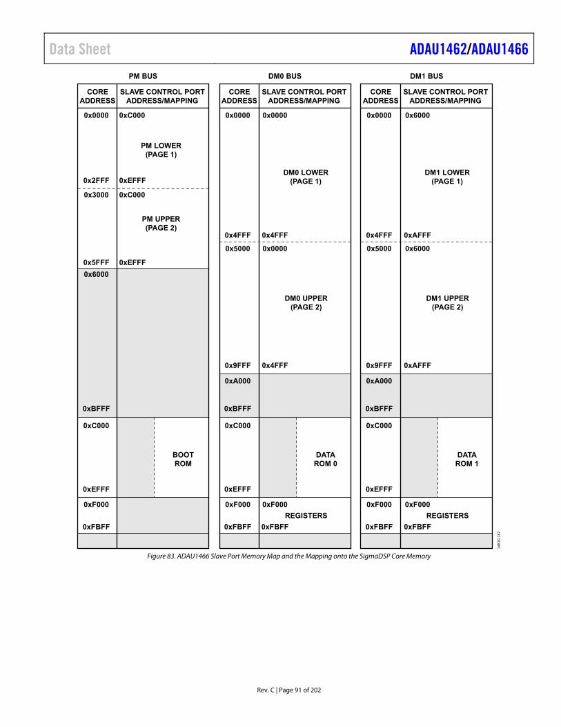
Data Sheet ADAU1462/ADAU1466
Rev. C | Page 91 of 202
148
10-
182
DM0 BUS
0x0000
0x4FFF
0x5000
DM0 LOWER(PAGE 1)
DM0 UPPER(PAGE 2)
REGISTERS
DATAROM 0
0xC000
0xEFFF
0xF000
0xFBFF
0xBFFF
0xA000
0x9FFF
0x0000
0x4FFF
0x0000
0x4FFF
COREADDRESS
SLAVE CONTROL PORTADDRESS/MAPPING
DM1 BUS
0x0000
0x4FFF
0x5000
DM1 LOWER(PAGE 1)
DM1 UPPER(PAGE 2)
REGISTERS
DATAROM 1
0xC000
0xEFFF
0xF000
0xFBFF
0xF000
0xFBFF
0xF000
0xFBFF
0xBFFF
0xA000
0x9FFF
0x6000
0xAFFF
0x6000
0xAFFF
COREADDRESS
SLAVE CONTROL PORTADDRESS/MAPPING
PM BUS
0x0000
0x2FFF
0xC000
0xC000
PM LOWER(PAGE 1)
PM UPPER(PAGE 2)
0xEFFF
0x3000
BOOTROM
0x5FFF
0xC000
0xF000
0xFBFF
0xBFFF
0x6000
0xEFFF
0xEFFF
COREADDRESS
SLAVE CONTROL PORTADDRESS/MAPPING
Figure 83. ADAU1466 Slave Port Memory Map and the Mapping onto the SigmaDSP Core Memory

ADAU1462/ADAU1466 Data Sheet
Rev. C | Page 92 of 202
CONTROL REGISTERS All control registers store 16 bits (two bytes) of data. The register map is defined in Table 58.
Table 58. Control Register Summary Reg Name Bits Bit 7 Bit 6 Bit 5 Bit 4 Bit 3 Bit 2 Bit 1 Bit 0 Reset RW
0xF000 PLL_CTRL0 [15:8] RESERVED[8:1] 0x0060 RW
[7:0] RESERVED[0] PLL_FBDIVIDER
0xF001 PLL_CTRL1 [15:8] RESERVED[13:6] 0x0000 RW
[7:0] RESERVED[5:0] PLL_DIV
0xF002 PLL_CLK_SRC [15:8] RESERVED[14:7] 0x0000 RW
[7:0] RESERVED[6:0] CLKSRC
0xF003 PLL_ENABLE [15:8] RESERVED[14:7] 0x0000 RW
[7:0] RESERVED[6:0] PLL_ENABLE
0xF004 PLL_LOCK [15:8] RESERVED[14:7] 0x0000 R
[7:0] RESERVED[6:0] PLL_LOCK
0xF005 MCLK_OUT [15:8] RESERVED[12:5] 0x0000 R
[7:0] RESERVED[4:0] CLKOUT_RATE CLKOUT_ ENABLE
0xF006 PLL_WATCHDOG [15:8] RESERVED[14:7] 0x0001 R
[7:0] RESERVED[6:0] PLL_WATCHDOG
0xF00A DISABLE_AUTOLOCK [15:8] RESERVED[14:7] 0x0000 RW
[7:0] RESERVED[6:0] DISABLE_ AUTOLOCK
0xF020 CLK_GEN1_M [15:8] RESERVED CLOCKGEN1_ M[8]
0x0006 RW
[7:0] CLOCKGEN1_M[7:0]
0xF021 CLK_GEN1_N [15:8] RESERVED CLOCKGEN1_ N[8]
0x0001 RW
[7:0] CLOCKGEN1_N[7:0]
0xF022 CLK_GEN2_M [15:8] RESERVED CLOCKGEN2_ M[8]
0x0009 RW
[7:0] CLOCKGEN2_M[7:0]
0xF023 CLK_GEN2_N [15:8] RESERVED CLOCKGEN2_ N[8]
0x0001 RW
[7:0] CLOCKGEN2_N[7:0]
0xF024 CLK_GEN3_M [15:8] CLOCKGEN3_M[15:8] 0x0000 RW
[7:0] CLOCKGEN3_M[7:0]
0xF025 CLK_GEN3_N [15:8] CLOCKGEN3_N[15:8] 0x0000 RW
[7:0] CLOCKGEN3_N[7:0]
0xF026 CLK_GEN3_SRC [15:8] RESERVED[10:3] 0x000E RW
[7:0] RESERVED[2:0] CLK_GEN3_SRC FREF_PIN
0xF027 CLK_GEN3_LOCK [15:8] RESERVED[14:7] 0x0000 R
[7:0] RESERVED[6:0] GEN3_LOCK
0xF050 POWER_ENABLE0 [15:8] RESERVED CLK_GEN3_ PWR
CLK_GEN2_ PWR
CLK_GEN1_ PWR
ASRCBANK1_ PWR
ASRCBANK0_ PWR
0x0000 RW
[7:0] SOUT3_PWR SOUT2_PWR SOUT1_PWR SOUT0_PWR SIN3_PWR SIN2_PWR SIN1_PWR SIN0_PWR
0xF051 POWER_ENABLE1 [15:8] RESERVED[10:3] 0x0000 RW
[7:0] RESERVED[2:0] PDM1_PWR PDM0_PWR TX_PWR RX_PWR ADC_PWR
0xF100 ... 0xF107
ASRC_INPUTx [15:8] RESERVED 0x0000 RW
[7:0] ASRC_SIN_CHANNEL ASRC_SOURCE
0xF140 ... 0xF147
ASRC_OUT_RATEx [15:8] RESERVED[11:4] 0x0000 RW
[7:0] RESERVED[3:0] ASRC_RATE
0xF180 ... 0xF197
SOUT_SOURCEx [15:8] RESERVED[9:2] 0x0000 RW
[7:0] RESERVED[1:0] SOUT_ASRC_SELECT SOUT_SOURCE
0xF1C0 SPDIFTX_INPUT [15:8] RESERVED[13:6] 0x0000 RW
[7:0] RESERVED[5:0] SPDIFTX_SOURCE
0xF200 ... 0xF21C
SERIAL_BYTE_x_0 [15:8] LRCLK_SRC BCLK_SRC LRCLK_MODE LRCLK_POL 0x0000 RW
[7:0] BCLK_POL WORD_LEN DATA_FMT TDM_MODE
0xF201 ... 0xF21D
SERIAL_BYTE_x_1 [15:8] RESERVED[9:2] 0x0002 RW
[7:0] RESERVED[1:0] TRISTATE CLK_DOMAIN FS
0xF300 ... 0xF33F
FTDM_INx [15:8] RESERVED 0x0000 RW
[7:0] SLOT_ ENABLE_IN
REVERSE_IN_ BYTE
SERIAL_IN_ SEL
CHANNEL_IN_POS BYTE_IN_POS
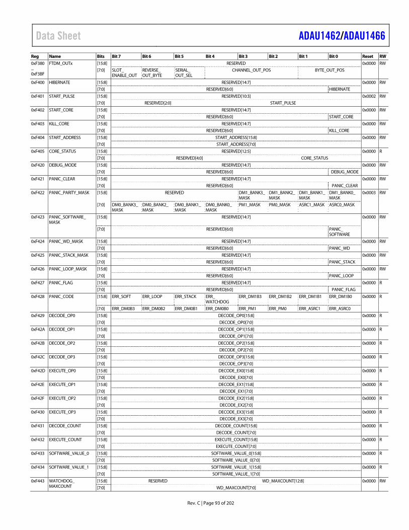
Data Sheet ADAU1462/ADAU1466
Rev. C | Page 93 of 202
Reg Name Bits Bit 7 Bit 6 Bit 5 Bit 4 Bit 3 Bit 2 Bit 1 Bit 0 Reset RW
0xF380 ... 0xF3BF
FTDM_OUTx [15:8] RESERVED 0x0000 RW
[7:0] SLOT_ ENABLE_OUT
REVERSE_ OUT_BYTE
SERIAL_ OUT_SEL
CHANNEL_OUT_POS BYTE_OUT_POS
0xF400 HIBERNATE [15:8] RESERVED[14:7] 0x0000 RW
[7:0] RESERVED[6:0] HIBERNATE
0xF401 START_PULSE [15:8] RESERVED[10:3] 0x0002 RW
[7:0] RESERVED[2:0] START_PULSE
0xF402 START_CORE [15:8] RESERVED[14:7] 0x0000 RW
[7:0] RESERVED[6:0] START_CORE
0xF403 KILL_CORE [15:8] RESERVED[14:7] 0x0000 RW
[7:0] RESERVED[6:0] KILL_CORE
0xF404 START_ADDRESS [15:8] START_ADDRESS[15:8] 0x0000 RW
[7:0] START_ADDRESS[7:0]
0xF405 CORE_STATUS [15:8] RESERVED[12:5] 0x0000 R
[7:0] RESERVED[4:0] CORE_STATUS
0xF420 DEBUG_MODE [15:8] RESERVED[14:7] 0x0000 RW
[7:0] RESERVED[6:0] DEBUG_MODE
0xF421 PANIC_CLEAR [15:8] RESERVED[14:7] 0x0000 RW
[7:0] RESERVED[6:0] PANIC_CLEAR
0xF422 PANIC_PARITY_MASK [15:8] RESERVED DM1_BANK3_MASK
DM1_BANK2_ MASK
DM1_BANK1_ MASK
DM1_BANK0_ MASK
0x0003 RW
[7:0] DM0_BANK3_ MASK
DM0_BANK2_ MASK
DM0_BANK1_MASK
DM0_BANK0_ MASK
PM1_MASK PM0_MASK ASRC1_MASK ASRC0_MASK
0xF423 PANIC_SOFTWARE_ MASK
[15:8] RESERVED[14:7] 0x0000 RW
[7:0] RESERVED[6:0] PANIC_ SOFTWARE
0xF424 PANIC_WD_MASK [15:8] RESERVED[14:7] 0x0000 RW
[7:0] RESERVED[6:0] PANIC_WD
0xF425 PANIC_STACK_MASK [15:8] RESERVED[14:7] 0x0000 RW
[7:0] RESERVED[6:0] PANIC_STACK
0xF426 PANIC_LOOP_MASK [15:8] RESERVED[14:7] 0x0000 RW
[7:0] RESERVED[6:0] PANIC_LOOP
0xF427 PANIC_FLAG [15:8] RESERVED[14:7] 0x0000 R
[7:0] RESERVED[6:0] PANIC_FLAG
0xF428 PANIC_CODE [15:8] ERR_SOFT ERR_LOOP ERR_STACK ERR_ WATCHDOG
ERR_DM1B3 ERR_DM1B2 ERR_DM1B1 ERR_DM1B0 0x0000 R
[7:0] ERR_DM0B3 ERR_DM0B2 ERR_DM0B1 ERR_DM0B0 ERR_PM1 ERR_PM0 ERR_ASRC1 ERR_ASRC0
0xF429 DECODE_OP0 [15:8] DECODE_OP0[15:8] 0x0000 R
[7:0] DECODE_OP0[7:0]
0xF42A DECODE_OP1 [15:8] DECODE_OP1[15:8] 0x0000 R
[7:0] DECODE_OP1[7:0]
0xF42B DECODE_OP2 [15:8] DECODE_OP2[15:8] 0x0000 R
[7:0] DECODE_OP2[7:0]
0xF42C DECODE_OP3 [15:8] DECODE_OP3[15:8] 0x0000 R
[7:0] DECODE_OP3[7:0]
0xF42D EXECUTE_OP0 [15:8] DECODE_EX0[15:8] 0x0000 R
[7:0] DECODE_EX0[7:0]
0xF42E EXECUTE_OP1 [15:8] DECODE_EX1[15:8] 0x0000 R
[7:0] DECODE_EX1[7:0]
0xF42F EXECUTE_OP2 [15:8] DECODE_EX2[15:8] 0x0000 R
[7:0] DECODE_EX2[7:0]
0xF430 EXECUTE_OP3 [15:8] DECODE_EX3[15:8] 0x0000 R
[7:0] DECODE_EX3[7:0]
0xF431 DECODE_COUNT [15:8] DECODE_COUNT[15:8] 0x0000 R
[7:0] DECODE_COUNT[7:0]
0xF432 EXECUTE_COUNT [15:8] EXECUTE_COUNT[15:8] 0x0000 R
[7:0] EXECUTE_COUNT[7:0]
0xF433 SOFTWARE_VALUE_0 [15:8] SOFTWARE_VALUE_0[15:8] 0x0000 R
[7:0] SOFTWARE_VALUE_0[7:0]
0xF434 SOFTWARE_VALUE_1 [15:8] SOFTWARE_VALUE_1[15:8] 0x0000 R
[7:0] SOFTWARE_VALUE_1[7:0]
0xF443 WATCHDOG_ MAXCOUNT
[15:8] RESERVED WD_MAXCOUNT[12:8] 0x0000 RW
[7:0] WD_MAXCOUNT[7:0]
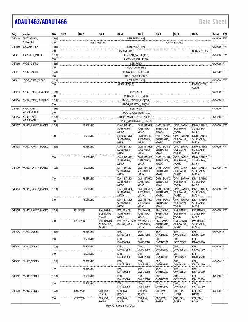
ADAU1462/ADAU1466 Data Sheet
Rev. C | Page 94 of 202
Reg Name Bits Bit 7 Bit 6 Bit 5 Bit 4 Bit 3 Bit 2 Bit 1 Bit 0 Reset RW
0xF444 WATCHDOG_ PRESCALE
[15:8] RESERVED[11:4] 0x0000 RW
[7:0] RESERVED[3:0] WD_PRESCALE
0xF450 BLOCKINT_EN [15:8] RESERVED[14:7] 0x0000 RW
[7:0] RESERVED[6:0] BLOCKINT_EN
0xF451 BLOCKINT_VALUE [15:8] BLOCKINT_VALUE[15:8] 0x0000 RW
[7:0] BLOCKINT_VALUE[7:0]
0xF460 PROG_CNTR0 [15:8] RESERVED 0x0000 R
[7:0] PROG_CNTR_MSB
0xF461 PROG_CNTR1 [15:8] PROG_CNTR_LSB[15:8] 0x0000 R
[7:0] PROG_CNTR_LSB[7:0]
0xF462 PROG_CNTR_CLEAR [15:8] RESERVED[14:7] 0x0000 RW
[7:0] RESERVED[6:0] PROG_CNTR_ CLEAR
0xF463 PROG_CNTR_LENGTH0 [15:8] RESERVED 0x0000 R
[7:0] PROG_LENGTH_MSB
0xF464 PROG_CNTR_LENGTH1 [15:8] PROG_LENGTH_LSB[15:8] 0x0000 R
[7:0] PROG_LENGTH_LSB[7:0]
0xF465 PROG_CNTR_ MAXLENGTH0
[15:8] RESERVED 0x0000 R
[7:0] PROG_MAXLENGTH_MSB
0xF466 PROG_CNTR_ MAXLENGTH1
[15:8] PROG_MAXLENGTH_LSB[15:8] 0x0000 R
[7:0] PROG_MAXLENGTH_LSB[7:0]
0xF467 PANIC_PARITY_MASK1 [15:8] RESERVED DM0_BANK1_ SUBBANK4_ MASK
DM0_BANK1_SUBBANK3_ MASK
DM0_BANK1_SUBBANK2_ MASK
DM0_BANK1_ SUBBANK1_ MASK
DM0_BANK1_ SUBBANK0_ MASK
0x0000 RW
[7:0] RESERVED DM0_BANK0_ SUBBANK4_ MASK
DM0_BANK0_SUBBANK3_ MASK
DM0_BANK0_SUBBANK2_ MASK
DM0_BANK0_ SUBBANK1_ MASK
DM0_BANK0_ SUBBANK0_ MASK
0xF468 PANIC_PARITY_MASK2 [15:8] RESERVED DM0_BANK3_ SUBBANK4_ MASK
DM0_BANK3_SUBBANK3_ MASK
DM0_BANK3_SUBBANK2_ MASK
DM0_BANK3_SUBBANK1_ MASK
DM0_BANK3_ SUBBANK0_ MASK
0x0000 RW
[7:0] RESERVED DM0_BANK2_ SUBBANK4_ MASK
DM0_BANK2_SUBBANK3_ MASK
DM0_BANK2_SUBBANK2_ MASK
DM0_BANK2_SUBBANK1_ MASK
DM0_BANK2_ SUBBANK0_ MASK
0xF469 PANIC_PARITY_MASK3 [15:8] RESERVED DM1_BANK1_ SUBBANK4_ MASK
DM1_BANK1_SUBBANK3_ MASK
DM1_BANK1_SUBBANK2_ MASK
DM1_BANK1_SUBBANK1_ MASK
DM1_BANK1_ SUBBANK0_ MASK
0x0000 RW
[7:0] RESERVED DM1_BANK0_ SUBBANK4_ MASK
DM1_BANK0_SUBBANK3_ MASK
DM1_BANK0_SUBBANK2_ MASK
DM1_BANK0_SUBBANK1_ MASK
DM1_BANK0_ SUBBANK0_ MASK
0xF46A PANIC_PARITY_MASK4 [15:8] RESERVED DM1_BANK3_ SUBBANK4_ MASK
DM1_BANK3_SUBBANK3_ MASK
DM1_BANK3_SUBBANK2_ MASK
DM1_BANK3_SUBBANK1_ MASK
DM1_BANK3_ SUBBANK0_ MASK
0x0000 RW
[7:0] RESERVED DM1_BANK2_ SUBBANK4_ MASK
DM1_BANK2_SUBBANK3_ MASK
DM1_BANK2_SUBBANK2_ MASK
DM1_BANK2_SUBBANK1_ MASK
DM1_BANK2_ SUBBANK0_ MASK
0xF46B PANIC_PARITY_MASK5 [15:8] RESERVED PM_BANK1_ SUBBANK5_ MASK
PM_BANK1_ SUBBANK4_ MASK
PM_BANK1_ SUBBANK3_ MASK
PM_BANK1_ SUBBANK2_ MASK
PM_BANK1_ SUBBANK1_ MASK
PM_BANK1_ SUBBANK0_ MASK
0x0000 RW
[7:0] RESERVED PM_BANK0_ SUBBANK5_ MASK
PM_BANK0_SUBBANK4_MASK
PM_BANK0_ SUBBANK3_ MASK
PM_BANK0_ SUBBANK2_ MASK
PM_BANK0_ SUBBANK1_ MASK
PM_BANK0_ SUBBANK0_ MASK
0xF46C PANIC_CODE1 [15:8] RESERVED ERR_ DM0B1SB4
ERR_ DM0B1SB3
ERR_ DM0B1SB2
ERR_ DM0B1SB1
ERR_ DM0B1SB0
0x0000 R
[7:0] RESERVED ERR_ DM0B0SB4
ERR_ DM0B0SB3
ERR_ DM0B0SB2
ERR_ DM0B0SB1
ERR_ DM0B0SB0
0xF46D PANIC_CODE2 [15:8] RESERVED ERR_ DM0B3SB4
ERR_ DM0B3SB3
ERR_ DM0B3SB2
ERR_ DM0B3SB1
ERR_ DM0B3SB0
0x0000 R
[7:0] RESERVED ERR_ DM0B2SB4
ERR_ DM0B2SB3
ERR_ DM0B2SB2
ERR_ DM0B2SB1
ERR_ DM0B2SB0
0xF46E PANIC_CODE3 [15:8] RESERVED ERR_ DM1B1SB4
ERR_ DM1B1SB3
ERR_ DM1B1SB2
ERR_ DM1B1SB1
ERR_ DM1B1SB0
0x0000 R
[7:0] RESERVED ERR_ DM1B0SB4
ERR_ DM1B0SB3
ERR_ DM1B0SB2
ERR_ DM1B0SB1
ERR_ DM1B0SB0
0xF46F PANIC_CODE4 [15:8] RESERVED ERR_ DM1B3SB4
ERR_ DM1B3SB3
ERR_ DM1B3SB2
ERR_ DM1B3SB1
ERR_ DM1B3SB0
0x0000 R
[7:0] RESERVED ERR_ DM1B2SB4
ERR_ DM1B2SB3
ERR_ DM1B2SB2
ERR_ DM1B2SB1
ERR_ DM1B2SB0
0xF470 PANIC_CODE5 [15:8] RESERVED ERR_PM_ B1SB5
ERR_PM_ B1SB4
ERR_PM_ B1SB3
ERR_PM_ B1SB2
ERR_PM_ B1SB1
ERR_PM_ B1SB0
0x0000 R
[7:0] RESERVED ERR_PM_ B0SB5
ERR_PM_ B0SB4
ERR_PM_ B0SB3
ERR_PM_ B0SB2
ERR_PM_ B0SB1
ERR_PM_ B0SB0
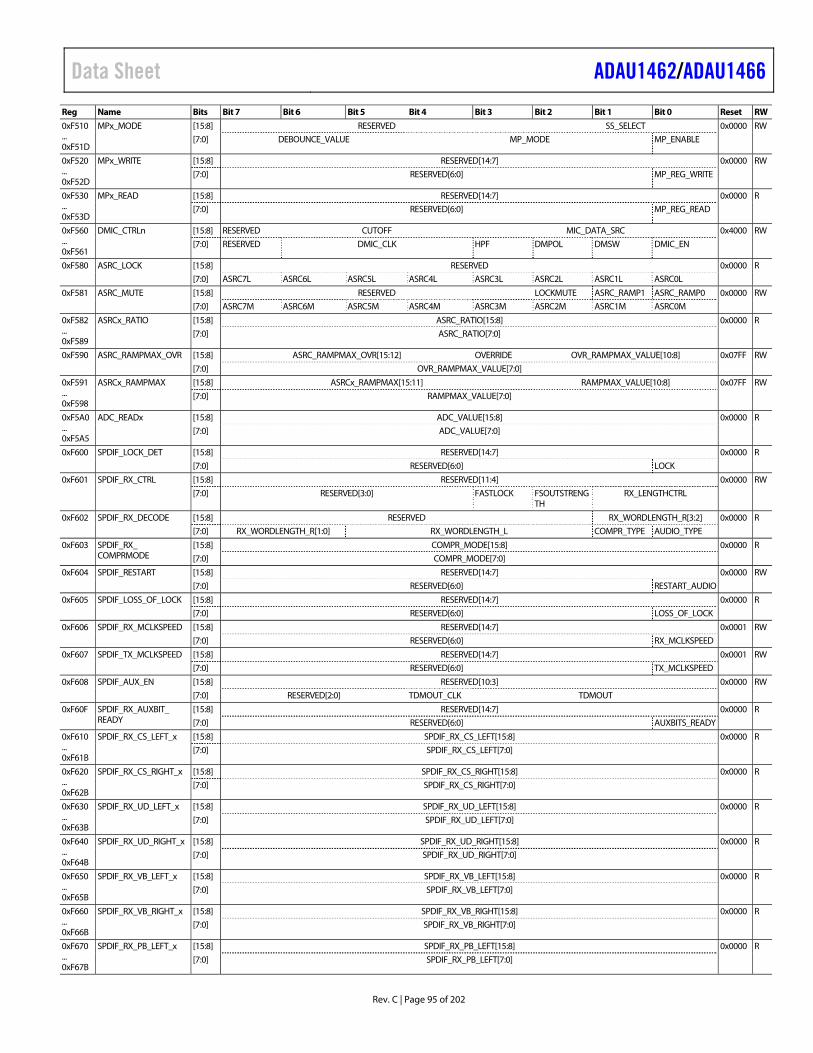
Data Sheet ADAU1462/ADAU1466
Rev. C | Page 95 of 202
Reg Name Bits Bit 7 Bit 6 Bit 5 Bit 4 Bit 3 Bit 2 Bit 1 Bit 0 Reset RW
0xF510 ... 0xF51D
MPx_MODE [15:8] RESERVED SS_SELECT 0x0000 RW
[7:0] DEBOUNCE_VALUE MP_MODE MP_ENABLE
0xF520 ... 0xF52D
MPx_WRITE [15:8] RESERVED[14:7] 0x0000 RW
[7:0] RESERVED[6:0] MP_REG_WRITE
0xF530 ... 0xF53D
MPx_READ [15:8] RESERVED[14:7] 0x0000 R
[7:0] RESERVED[6:0] MP_REG_READ
0xF560 ... 0xF561
DMIC_CTRLn [15:8] RESERVED CUTOFF MIC_DATA_SRC 0x4000 RW
[7:0] RESERVED DMIC_CLK HPF DMPOL DMSW DMIC_EN
0xF580 ASRC_LOCK [15:8] RESERVED 0x0000 R
[7:0] ASRC7L ASRC6L ASRC5L ASRC4L ASRC3L ASRC2L ASRC1L ASRC0L
0xF581 ASRC_MUTE [15:8] RESERVED LOCKMUTE ASRC_RAMP1 ASRC_RAMP0 0x0000 RW
[7:0] ASRC7M ASRC6M ASRC5M ASRC4M ASRC3M ASRC2M ASRC1M ASRC0M
0xF582 ... 0xF589
ASRCx_RATIO [15:8] ASRC_RATIO[15:8] 0x0000 R
[7:0] ASRC_RATIO[7:0]
0xF590 ASRC_RAMPMAX_OVR [15:8] ASRC_RAMPMAX_OVR[15:12] OVERRIDE OVR_RAMPMAX_VALUE[10:8] 0x07FF RW
[7:0] OVR_RAMPMAX_VALUE[7:0]
0xF591 ... 0xF598
ASRCx_RAMPMAX [15:8] ASRCx_RAMPMAX[15:11] RAMPMAX_VALUE[10:8] 0x07FF RW
[7:0] RAMPMAX_VALUE[7:0]
0xF5A0 ... 0xF5A5
ADC_READx [15:8] ADC_VALUE[15:8] 0x0000 R
[7:0] ADC_VALUE[7:0]
0xF600 SPDIF_LOCK_DET [15:8] RESERVED[14:7] 0x0000 R
[7:0] RESERVED[6:0] LOCK
0xF601 SPDIF_RX_CTRL [15:8] RESERVED[11:4] 0x0000 RW
[7:0] RESERVED[3:0] FASTLOCK FSOUTSTRENGTH
RX_LENGTHCTRL
0xF602 SPDIF_RX_DECODE [15:8] RESERVED RX_WORDLENGTH_R[3:2] 0x0000 R
[7:0] RX_WORDLENGTH_R[1:0] RX_WORDLENGTH_L COMPR_TYPE AUDIO_TYPE
0xF603 SPDIF_RX_ COMPRMODE
[15:8] COMPR_MODE[15:8] 0x0000 R
[7:0] COMPR_MODE[7:0]
0xF604 SPDIF_RESTART [15:8] RESERVED[14:7] 0x0000 RW
[7:0] RESERVED[6:0] RESTART_AUDIO
0xF605 SPDIF_LOSS_OF_LOCK [15:8] RESERVED[14:7] 0x0000 R
[7:0] RESERVED[6:0] LOSS_OF_LOCK
0xF606 SPDIF_RX_MCLKSPEED [15:8] RESERVED[14:7] 0x0001 RW
[7:0] RESERVED[6:0] RX_MCLKSPEED
0xF607 SPDIF_TX_MCLKSPEED [15:8] RESERVED[14:7] 0x0001 RW
[7:0] RESERVED[6:0] TX_MCLKSPEED
0xF608 SPDIF_AUX_EN [15:8] RESERVED[10:3] 0x0000 RW
[7:0] RESERVED[2:0] TDMOUT_CLK TDMOUT
0xF60F SPDIF_RX_AUXBIT_ READY
[15:8] RESERVED[14:7] 0x0000 R
[7:0] RESERVED[6:0] AUXBITS_READY
0xF610 ... 0xF61B
SPDIF_RX_CS_LEFT_x [15:8] SPDIF_RX_CS_LEFT[15:8] 0x0000 R
[7:0] SPDIF_RX_CS_LEFT[7:0]
0xF620 ... 0xF62B
SPDIF_RX_CS_RIGHT_x [15:8] SPDIF_RX_CS_RIGHT[15:8] 0x0000 R
[7:0] SPDIF_RX_CS_RIGHT[7:0]
0xF630 ... 0xF63B
SPDIF_RX_UD_LEFT_x [15:8] SPDIF_RX_UD_LEFT[15:8] 0x0000 R
[7:0] SPDIF_RX_UD_LEFT[7:0]
0xF640 ... 0xF64B
SPDIF_RX_UD_RIGHT_x [15:8] SPDIF_RX_UD_RIGHT[15:8] 0x0000 R
[7:0] SPDIF_RX_UD_RIGHT[7:0]
0xF650 ... 0xF65B
SPDIF_RX_VB_LEFT_x [15:8] SPDIF_RX_VB_LEFT[15:8] 0x0000 R
[7:0] SPDIF_RX_VB_LEFT[7:0]
0xF660 ... 0xF66B
SPDIF_RX_VB_RIGHT_x [15:8] SPDIF_RX_VB_RIGHT[15:8] 0x0000 R
[7:0] SPDIF_RX_VB_RIGHT[7:0]
0xF670 ... 0xF67B
SPDIF_RX_PB_LEFT_x [15:8] SPDIF_RX_PB_LEFT[15:8] 0x0000 R
[7:0] SPDIF_RX_PB_LEFT[7:0]
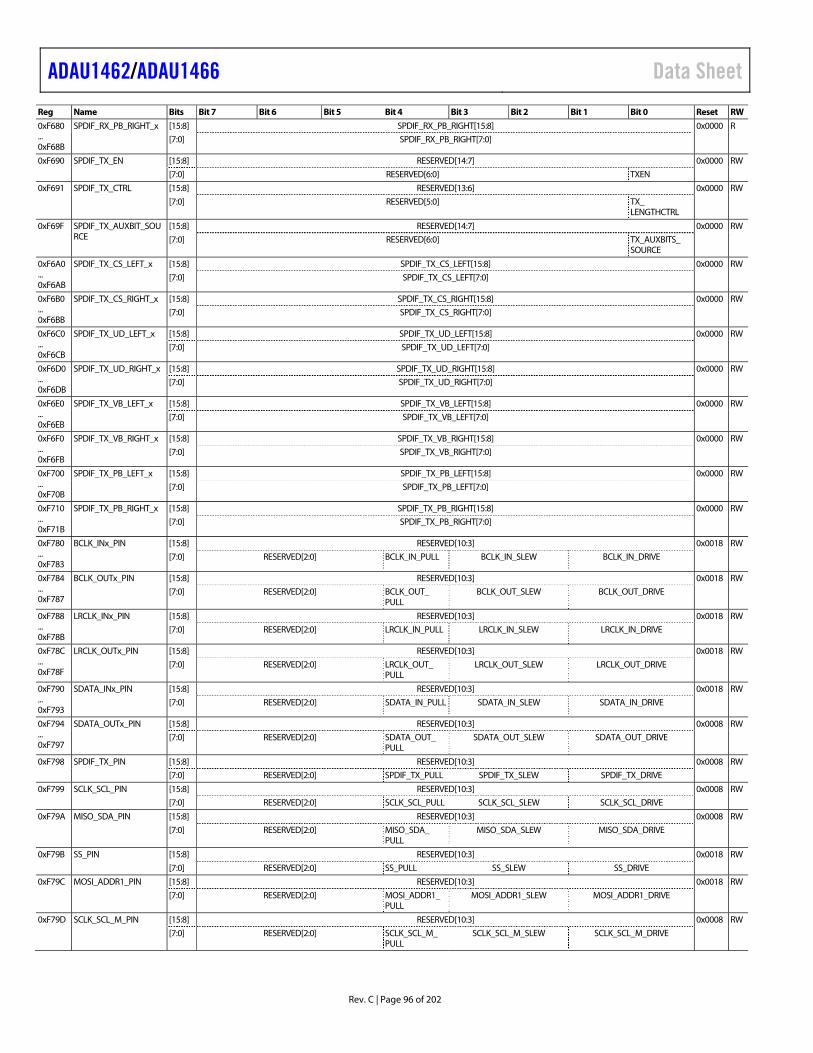
ADAU1462/ADAU1466 Data Sheet
Rev. C | Page 96 of 202
Reg Name Bits Bit 7 Bit 6 Bit 5 Bit 4 Bit 3 Bit 2 Bit 1 Bit 0 Reset RW
0xF680 ... 0xF68B
SPDIF_RX_PB_RIGHT_x [15:8] SPDIF_RX_PB_RIGHT[15:8] 0x0000 R
[7:0] SPDIF_RX_PB_RIGHT[7:0]
0xF690 SPDIF_TX_EN [15:8] RESERVED[14:7] 0x0000 RW
[7:0] RESERVED[6:0] TXEN
0xF691 SPDIF_TX_CTRL [15:8] RESERVED[13:6] 0x0000 RW
[7:0] RESERVED[5:0] TX_ LENGTHCTRL
0xF69F SPDIF_TX_AUXBIT_SOURCE
[15:8] RESERVED[14:7] 0x0000 RW
[7:0] RESERVED[6:0] TX_AUXBITS_ SOURCE
0xF6A0 ... 0xF6AB
SPDIF_TX_CS_LEFT_x [15:8] SPDIF_TX_CS_LEFT[15:8] 0x0000 RW
[7:0] SPDIF_TX_CS_LEFT[7:0]
0xF6B0 ... 0xF6BB
SPDIF_TX_CS_RIGHT_x [15:8] SPDIF_TX_CS_RIGHT[15:8] 0x0000 RW
[7:0] SPDIF_TX_CS_RIGHT[7:0]
0xF6C0 ... 0xF6CB
SPDIF_TX_UD_LEFT_x [15:8] SPDIF_TX_UD_LEFT[15:8] 0x0000 RW
[7:0] SPDIF_TX_UD_LEFT[7:0]
0xF6D0 ... 0xF6DB
SPDIF_TX_UD_RIGHT_x [15:8] SPDIF_TX_UD_RIGHT[15:8] 0x0000 RW
[7:0] SPDIF_TX_UD_RIGHT[7:0]
0xF6E0 ... 0xF6EB
SPDIF_TX_VB_LEFT_x [15:8] SPDIF_TX_VB_LEFT[15:8] 0x0000 RW
[7:0] SPDIF_TX_VB_LEFT[7:0]
0xF6F0 ... 0xF6FB
SPDIF_TX_VB_RIGHT_x [15:8] SPDIF_TX_VB_RIGHT[15:8] 0x0000 RW
[7:0] SPDIF_TX_VB_RIGHT[7:0]
0xF700 ... 0xF70B
SPDIF_TX_PB_LEFT_x [15:8] SPDIF_TX_PB_LEFT[15:8] 0x0000 RW
[7:0] SPDIF_TX_PB_LEFT[7:0]
0xF710 ... 0xF71B
SPDIF_TX_PB_RIGHT_x [15:8] SPDIF_TX_PB_RIGHT[15:8] 0x0000 RW
[7:0] SPDIF_TX_PB_RIGHT[7:0]
0xF780 ... 0xF783
BCLK_INx_PIN [15:8] RESERVED[10:3] 0x0018 RW
[7:0] RESERVED[2:0] BCLK_IN_PULL BCLK_IN_SLEW BCLK_IN_DRIVE
0xF784 ... 0xF787
BCLK_OUTx_PIN [15:8] RESERVED[10:3] 0x0018 RW
[7:0] RESERVED[2:0] BCLK_OUT_ PULL
BCLK_OUT_SLEW BCLK_OUT_DRIVE
0xF788 ... 0xF78B
LRCLK_INx_PIN [15:8] RESERVED[10:3] 0x0018 RW
[7:0] RESERVED[2:0] LRCLK_IN_PULL LRCLK_IN_SLEW LRCLK_IN_DRIVE
0xF78C ... 0xF78F
LRCLK_OUTx_PIN [15:8] RESERVED[10:3] 0x0018 RW
[7:0] RESERVED[2:0] LRCLK_OUT_ PULL
LRCLK_OUT_SLEW LRCLK_OUT_DRIVE
0xF790 ... 0xF793
SDATA_INx_PIN [15:8] RESERVED[10:3] 0x0018 RW
[7:0] RESERVED[2:0] SDATA_IN_PULL SDATA_IN_SLEW SDATA_IN_DRIVE
0xF794 ... 0xF797
SDATA_OUTx_PIN [15:8] RESERVED[10:3] 0x0008 RW
[7:0] RESERVED[2:0] SDATA_OUT_ PULL
SDATA_OUT_SLEW SDATA_OUT_DRIVE
0xF798 SPDIF_TX_PIN [15:8] RESERVED[10:3] 0x0008 RW
[7:0] RESERVED[2:0] SPDIF_TX_PULL SPDIF_TX_SLEW SPDIF_TX_DRIVE
0xF799 SCLK_SCL_PIN [15:8] RESERVED[10:3] 0x0008 RW
[7:0] RESERVED[2:0] SCLK_SCL_PULL SCLK_SCL_SLEW SCLK_SCL_DRIVE
0xF79A MISO_SDA_PIN [15:8] RESERVED[10:3] 0x0008 RW
[7:0] RESERVED[2:0] MISO_SDA_ PULL
MISO_SDA_SLEW MISO_SDA_DRIVE
0xF79B SS_PIN [15:8] RESERVED[10:3] 0x0018 RW
[7:0] RESERVED[2:0] SS_PULL SS_SLEW SS_DRIVE
0xF79C MOSI_ADDR1_PIN [15:8] RESERVED[10:3] 0x0018 RW
[7:0] RESERVED[2:0] MOSI_ADDR1_ PULL
MOSI_ADDR1_SLEW MOSI_ADDR1_DRIVE
0xF79D SCLK_SCL_M_PIN [15:8] RESERVED[10:3] 0x0008 RW
[7:0] RESERVED[2:0] SCLK_SCL_M_ PULL
SCLK_SCL_M_SLEW SCLK_SCL_M_DRIVE
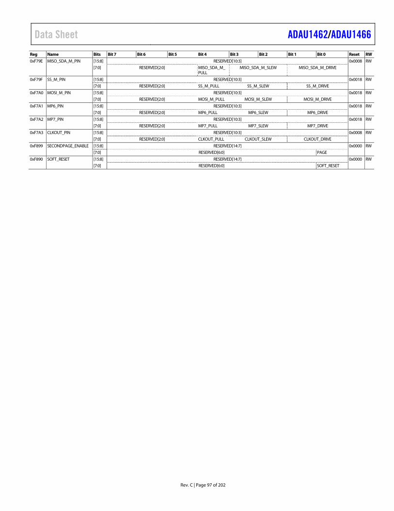
Data Sheet ADAU1462/ADAU1466
Rev. C | Page 97 of 202
Reg Name Bits Bit 7 Bit 6 Bit 5 Bit 4 Bit 3 Bit 2 Bit 1 Bit 0 Reset RW
0xF79E MISO_SDA_M_PIN [15:8] RESERVED[10:3] 0x0008 RW
[7:0] RESERVED[2:0] MISO_SDA_M_ PULL
MISO_SDA_M_SLEW MISO_SDA_M_DRIVE
0xF79F SS_M_PIN [15:8] RESERVED[10:3] 0x0018 RW
[7:0] RESERVED[2:0] SS_M_PULL SS_M_SLEW SS_M_DRIVE
0xF7A0 MOSI_M_PIN [15:8] RESERVED[10:3] 0x0018 RW
[7:0] RESERVED[2:0] MOSI_M_PULL MOSI_M_SLEW MOSI_M_DRIVE
0xF7A1 MP6_PIN [15:8] RESERVED[10:3] 0x0018 RW
[7:0] RESERVED[2:0] MP6_PULL MP6_SLEW MP6_DRIVE
0xF7A2 MP7_PIN [15:8] RESERVED[10:3] 0x0018 RW
[7:0] RESERVED[2:0] MP7_PULL MP7_SLEW MP7_DRIVE
0xF7A3 CLKOUT_PIN [15:8] RESERVED[10:3] 0x0008 RW
[7:0] RESERVED[2:0] CLKOUT_PULL CLKOUT_SLEW CLKOUT_DRIVE
0xF899 SECONDPAGE_ENABLE [15:8] RESERVED[14:7] 0x0000 RW
[7:0] RESERVED[6:0] PAGE
0xF890 SOFT_RESET [15:8] RESERVED[14:7] 0x0000 RW
[7:0] RESERVED[6:0] SOFT_RESET
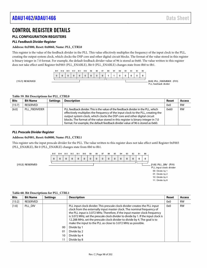
ADAU1462/ADAU1466 Data Sheet
Rev. C | Page 98 of 202
CONTROL REGISTER DETAILS PLL CONFIGURATION REGISTERS PLL Feedback Divider Register
Address: 0xF000, Reset: 0x0060, Name: PLL_CTRL0
This register is the value of the feedback divider in the PLL. This value effectively multiplies the frequency of the input clock to the PLL, creating the output system clock, which clocks the DSP core and other digital circuit blocks. The format of the value stored in this register is binary integer in 7.0 format. For example, the default feedback divider value of 96 is stored as 0x60. The value written to this register does not take effect until Register 0xF003 (PLL_ENABLE), Bit 0 (PLL_ENABLE) changes state from 0b0 to 0b1.
Table 59. Bit Descriptions for PLL_CTRL0 Bits Bit Name Settings Description Reset Access [15:7] RESERVED 0x0 RW [6:0] PLL_FBDIVIDER PLL feedback divider. This is the value of the feedback divider in the PLL, which
effectively multiplies the frequency of the input clock to the PLL, creating the output system clock, which clocks the DSP core and other digital circuit blocks. The format of the value stored in this register is binary integer in 7.0 format. For example, the default feedback divider value of 96 is stored as 0x60.
0x60 RW
PLL Prescale Divider Register
Address: 0xF001, Reset: 0x0000, Name: PLL_CTRL1
This register sets the input prescale divider for the PLL. The value written to this register does not take effect until Register 0xF003 (PLL_ENABLE), Bit 0 (PLL_ENABLE) changes state from 0b0 to 0b1.
Table 60. Bit Descriptions for PLL_CTRL1 Bits Bit Name Settings Description Reset Access [15:2] RESERVED 0x0 RW [1:0] PLL_DIV PLL input clock divider. This prescale clock divider creates the PLL input
clock from the externally input master clock. The nominal frequency of the PLL input is 3.072 MHz. Therefore, if the input master clock frequency is 3.072 MHz, set the prescale clock divider to divide by 1. If the input clock is 12.288 MHz, set the prescale clock divider to divide by 4. The goal is to make the input to the PLL as close to 3.072 MHz as possible.
0x0 RW
00 Divide by 1 01 Divide by 2 10 Divide by 4 11 Divide by 8
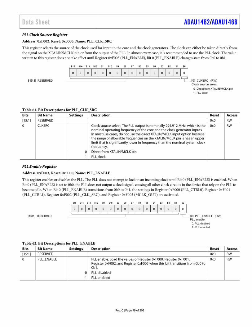
Data Sheet ADAU1462/ADAU1466
Rev. C | Page 99 of 202
PLL Clock Source Register
Address: 0xF002, Reset: 0x0000, Name: PLL_CLK_SRC
This register selects the source of the clock used for input to the core and the clock generators. The clock can either be taken directly from the signal on the XTALIN/MCLK pin or from the output of the PLL. In almost every case, it is recommended to use the PLL clock. The value written to this register does not take effect until Register 0xF003 (PLL_ENABLE), Bit 0 (PLL_ENABLE) changes state from 0b0 to 0b1.
Table 61. Bit Descriptions for PLL_CLK_SRC Bits Bit Name Settings Description Reset Access [15:1] RESERVED 0x0 RW 0 CLKSRC Clock source select. The PLL output is nominally 294.912 MHz, which is the
nominal operating frequency of the core and the clock generator inputs. In most use cases, do not use the direct XTALIN/MCLK input option because the range of allowable frequencies on the XTALIN/MCLK pin is has an upper limit that is significantly lower in frequency than the nominal system clock frequency.
0x0 RW
0 Direct from XTALIN/MCLK pin 1 PLL clock
PLL Enable Register
Address: 0xF003, Reset: 0x0000, Name: PLL_ENABLE
This register enables or disables the PLL. The PLL does not attempt to lock to an incoming clock until Bit 0 (PLL_ENABLE) is enabled. When Bit 0 (PLL_ENABLE) is set to 0b0, the PLL does not output a clock signal, causing all other clock circuits in the device that rely on the PLL to become idle. When Bit 0 (PLL_ENABLE) transitions from 0b0 to 0b1, the settings in Register 0xF000 (PLL_CTRL0), Register 0xF001 (PLL_CTRL1), Register 0xF002 (PLL_CLK_SRC), and Register 0xF005 (MCLK_OUT) are activated.
Table 62. Bit Descriptions for PLL_ENABLE Bits Bit Name Settings Description Reset Access [15:1] RESERVED 0x0 RW 0 PLL_ENABLE PLL enable. Load the values of Register 0xF000, Register 0xF001,
Register 0xF002, and Register 0xF005 when this bit transitions from 0b0 to 0b1.
0x0 RW
0 PLL disabled 1 PLL enabled
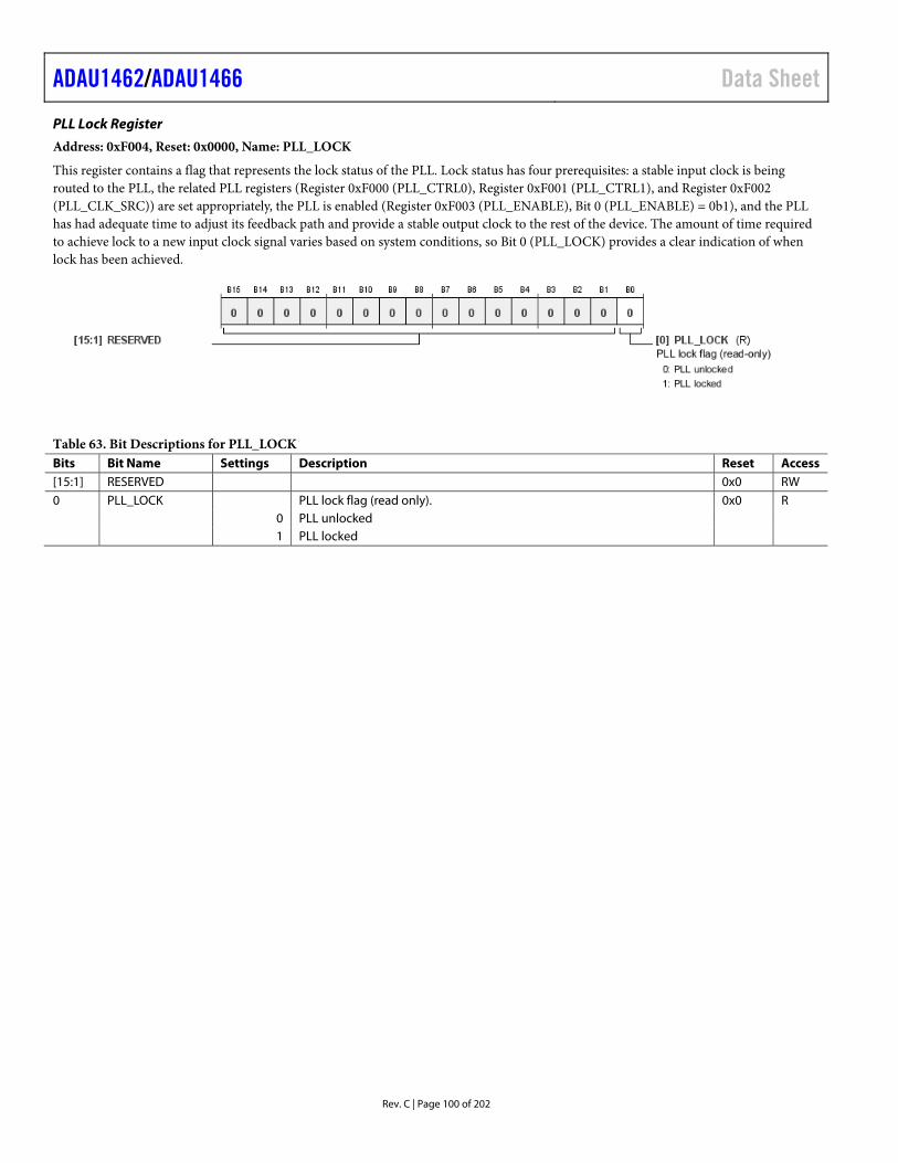
ADAU1462/ADAU1466 Data Sheet
Rev. C | Page 100 of 202
PLL Lock Register
Address: 0xF004, Reset: 0x0000, Name: PLL_LOCK
This register contains a flag that represents the lock status of the PLL. Lock status has four prerequisites: a stable input clock is being routed to the PLL, the related PLL registers (Register 0xF000 (PLL_CTRL0), Register 0xF001 (PLL_CTRL1), and Register 0xF002 (PLL_CLK_SRC)) are set appropriately, the PLL is enabled (Register 0xF003 (PLL_ENABLE), Bit 0 (PLL_ENABLE) = 0b1), and the PLL has had adequate time to adjust its feedback path and provide a stable output clock to the rest of the device. The amount of time required to achieve lock to a new input clock signal varies based on system conditions, so Bit 0 (PLL_LOCK) provides a clear indication of when lock has been achieved.
Table 63. Bit Descriptions for PLL_LOCK Bits Bit Name Settings Description Reset Access [15:1] RESERVED 0x0 RW 0 PLL_LOCK PLL lock flag (read only). 0x0 R 0 PLL unlocked 1 PLL locked
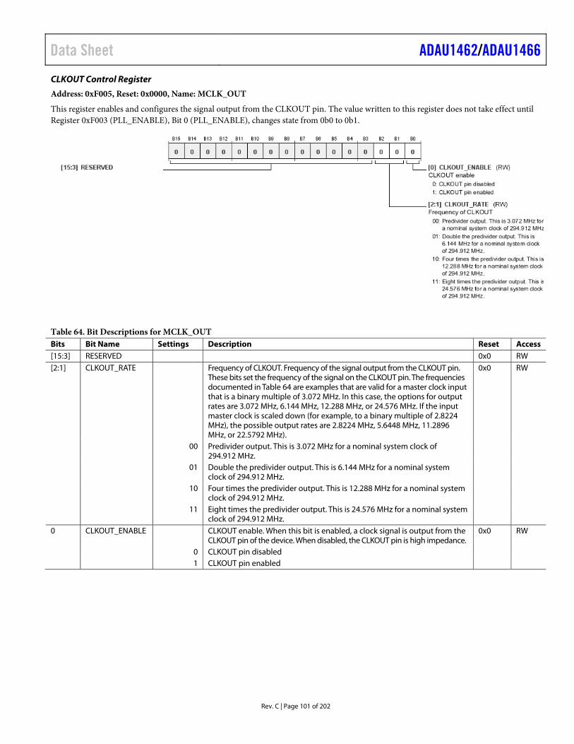
Data Sheet ADAU1462/ADAU1466
Rev. C | Page 101 of 202
CLKOUT Control Register
Address: 0xF005, Reset: 0x0000, Name: MCLK_OUT
This register enables and configures the signal output from the CLKOUT pin. The value written to this register does not take effect until Register 0xF003 (PLL_ENABLE), Bit 0 (PLL_ENABLE), changes state from 0b0 to 0b1.
Table 64. Bit Descriptions for MCLK_OUT Bits Bit Name Settings Description Reset Access [15:3] RESERVED 0x0 RW [2:1] CLKOUT_RATE Frequency of CLKOUT. Frequency of the signal output from the CLKOUT pin.
These bits set the frequency of the signal on the CLKOUT pin. The frequencies documented in Table 64 are examples that are valid for a master clock input that is a binary multiple of 3.072 MHz. In this case, the options for output rates are 3.072 MHz, 6.144 MHz, 12.288 MHz, or 24.576 MHz. If the input master clock is scaled down (for example, to a binary multiple of 2.8224 MHz), the possible output rates are 2.8224 MHz, 5.6448 MHz, 11.2896 MHz, or 22.5792 MHz).
0x0 RW
00 Predivider output. This is 3.072 MHz for a nominal system clock of 294.912 MHz.
01 Double the predivider output. This is 6.144 MHz for a nominal system clock of 294.912 MHz.
10 Four times the predivider output. This is 12.288 MHz for a nominal system clock of 294.912 MHz.
11 Eight times the predivider output. This is 24.576 MHz for a nominal system clock of 294.912 MHz.
0 CLKOUT_ENABLE CLKOUT enable. When this bit is enabled, a clock signal is output from the CLKOUT pin of the device. When disabled, the CLKOUT pin is high impedance.
0x0 RW
0 CLKOUT pin disabled 1 CLKOUT pin enabled
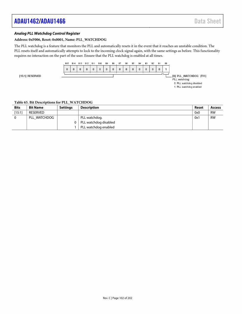
ADAU1462/ADAU1466 Data Sheet
Rev. C | Page 102 of 202
Analog PLL Watchdog Control Register
Address: 0xF006, Reset: 0x0001, Name: PLL_WATCHDOG
The PLL watchdog is a feature that monitors the PLL and automatically resets it in the event that it reaches an unstable condition. The PLL resets itself and automatically attempts to lock to the incoming clock signal again, with the same settings as before. This functionality requires no interaction on the part of the user. Ensure that the PLL watchdog is enabled at all times.
Table 65. Bit Descriptions for PLL_WATCHDOG Bits Bit Name Settings Description Reset Access [15:1] RESERVED 0x0 RW 0 PLL_WATCHDOG PLL watchdog. 0x1 RW 0 PLL watchdog disabled 1 PLL watchdog enabled
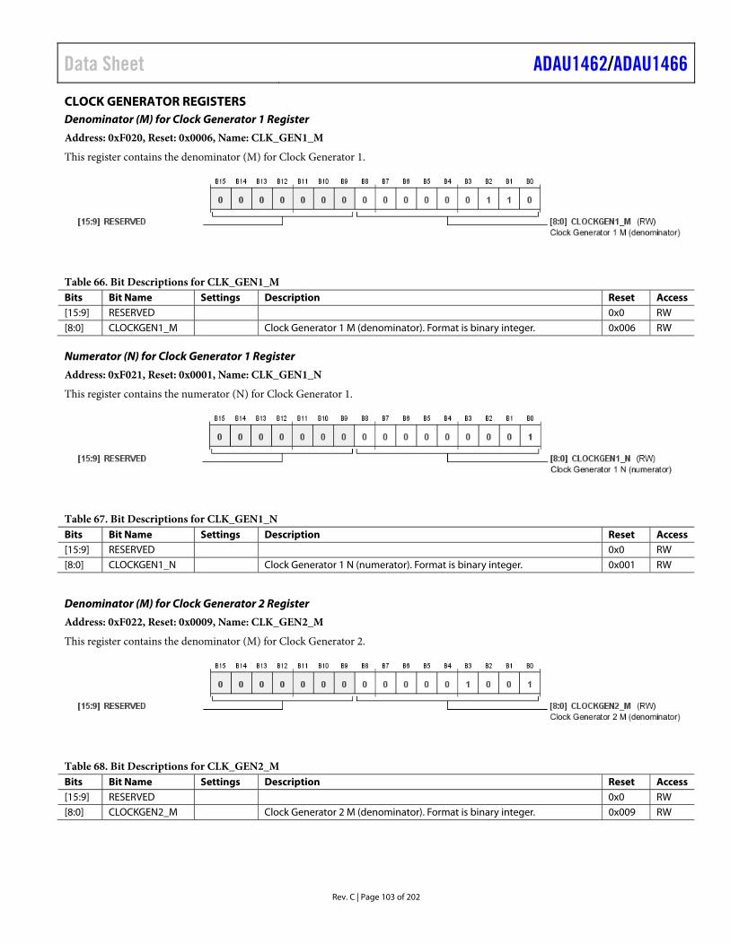
Data Sheet ADAU1462/ADAU1466
Rev. C | Page 103 of 202
CLOCK GENERATOR REGISTERS Denominator (M) for Clock Generator 1 Register
Address: 0xF020, Reset: 0x0006, Name: CLK_GEN1_M
This register contains the denominator (M) for Clock Generator 1.
Table 66. Bit Descriptions for CLK_GEN1_M Bits Bit Name Settings Description Reset Access [15:9] RESERVED 0x0 RW [8:0] CLOCKGEN1_M Clock Generator 1 M (denominator). Format is binary integer. 0x006 RW
Numerator (N) for Clock Generator 1 Register
Address: 0xF021, Reset: 0x0001, Name: CLK_GEN1_N
This register contains the numerator (N) for Clock Generator 1.
Table 67. Bit Descriptions for CLK_GEN1_N Bits Bit Name Settings Description Reset Access [15:9] RESERVED 0x0 RW [8:0] CLOCKGEN1_N Clock Generator 1 N (numerator). Format is binary integer. 0x001 RW
Denominator (M) for Clock Generator 2 Register
Address: 0xF022, Reset: 0x0009, Name: CLK_GEN2_M
This register contains the denominator (M) for Clock Generator 2.
Table 68. Bit Descriptions for CLK_GEN2_M Bits Bit Name Settings Description Reset Access [15:9] RESERVED 0x0 RW [8:0] CLOCKGEN2_M Clock Generator 2 M (denominator). Format is binary integer. 0x009 RW
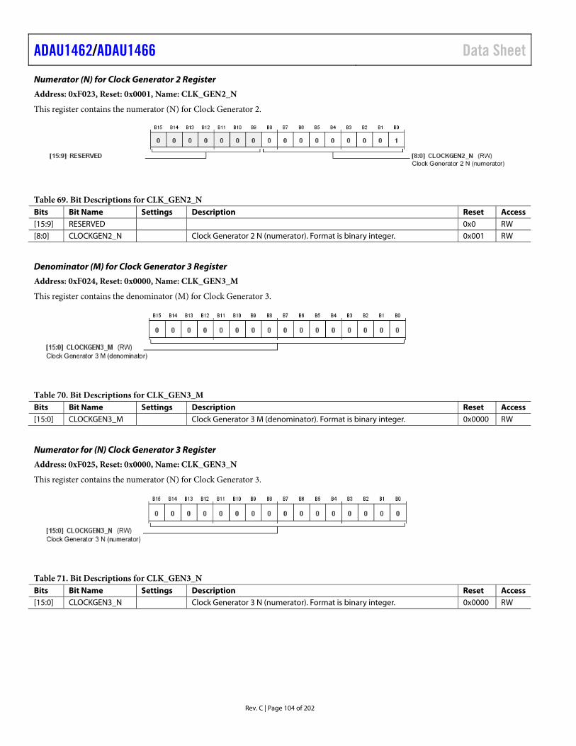
ADAU1462/ADAU1466 Data Sheet
Rev. C | Page 104 of 202
Numerator (N) for Clock Generator 2 Register
Address: 0xF023, Reset: 0x0001, Name: CLK_GEN2_N
This register contains the numerator (N) for Clock Generator 2.
Table 69. Bit Descriptions for CLK_GEN2_N Bits Bit Name Settings Description Reset Access [15:9] RESERVED 0x0 RW [8:0] CLOCKGEN2_N Clock Generator 2 N (numerator). Format is binary integer. 0x001 RW
Denominator (M) for Clock Generator 3 Register
Address: 0xF024, Reset: 0x0000, Name: CLK_GEN3_M
This register contains the denominator (M) for Clock Generator 3.
Table 70. Bit Descriptions for CLK_GEN3_M Bits Bit Name Settings Description Reset Access [15:0] CLOCKGEN3_M Clock Generator 3 M (denominator). Format is binary integer. 0x0000 RW
Numerator for (N) Clock Generator 3 Register
Address: 0xF025, Reset: 0x0000, Name: CLK_GEN3_N
This register contains the numerator (N) for Clock Generator 3.
Table 71. Bit Descriptions for CLK_GEN3_N Bits Bit Name Settings Description Reset Access [15:0] CLOCKGEN3_N Clock Generator 3 N (numerator). Format is binary integer. 0x0000 RW
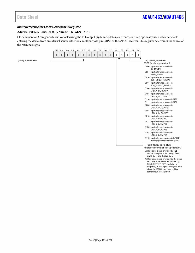
Data Sheet ADAU1462/ADAU1466
Rev. C | Page 105 of 202
Input Reference for Clock Generator 3 Register
Address: 0xF026, Reset: 0x000E, Name: CLK_GEN3_SRC
Clock Generator 3 can generate audio clocks using the PLL output (system clock) as a reference, or it can optionally use a reference clock entering the device from an external source either on a multipurpose pin (MPx) or the S/PDIF receiver. This register determines the source of the reference signal.
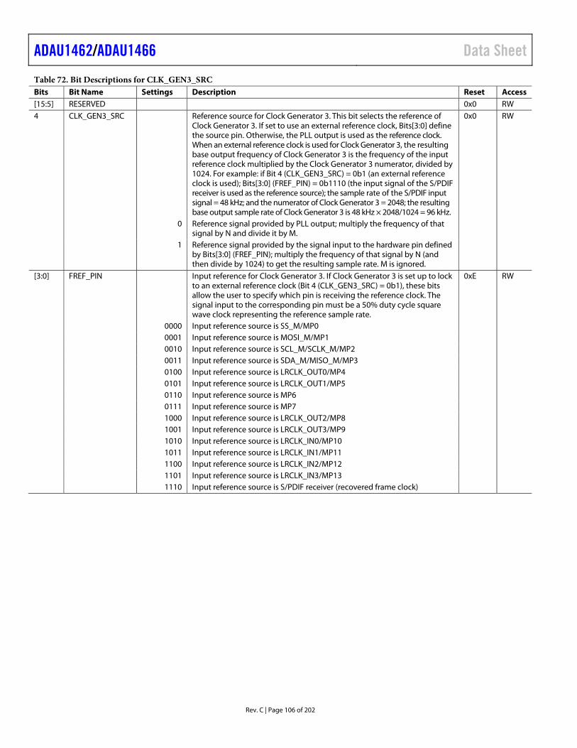
ADAU1462/ADAU1466 Data Sheet
Rev. C | Page 106 of 202
Table 72. Bit Descriptions for CLK_GEN3_SRC Bits Bit Name Settings Description Reset Access [15:5] RESERVED 0x0 RW 4 CLK_GEN3_SRC Reference source for Clock Generator 3. This bit selects the reference of
Clock Generator 3. If set to use an external reference clock, Bits[3:0] define the source pin. Otherwise, the PLL output is used as the reference clock. When an external reference clock is used for Clock Generator 3, the resulting base output frequency of Clock Generator 3 is the frequency of the input reference clock multiplied by the Clock Generator 3 numerator, divided by 1024. For example: if Bit 4 (CLK_GEN3_SRC) = 0b1 (an external reference clock is used); Bits[3:0] (FREF_PIN) = 0b1110 (the input signal of the S/PDIF receiver is used as the reference source); the sample rate of the S/PDIF input signal = 48 kHz; and the numerator of Clock Generator 3 = 2048; the resulting base output sample rate of Clock Generator 3 is 48 kHz × 2048/1024 = 96 kHz.
0x0 RW
0 Reference signal provided by PLL output; multiply the frequency of that signal by N and divide it by M.
1 Reference signal provided by the signal input to the hardware pin defined by Bits[3:0] (FREF_PIN); multiply the frequency of that signal by N (and then divide by 1024) to get the resulting sample rate. M is ignored.
[3:0] FREF_PIN Input reference for Clock Generator 3. If Clock Generator 3 is set up to lock to an external reference clock (Bit 4 (CLK_GEN3_SRC) = 0b1), these bits allow the user to specify which pin is receiving the reference clock. The signal input to the corresponding pin must be a 50% duty cycle square wave clock representing the reference sample rate.
0xE RW
0000 Input reference source is SS_M/MP0 0001 Input reference source is MOSI_M/MP1 0010 Input reference source is SCL_M/SCLK_M/MP2 0011 Input reference source is SDA_M/MISO_M/MP3 0100 Input reference source is LRCLK_OUT0/MP4 0101 Input reference source is LRCLK_OUT1/MP5 0110 Input reference source is MP6 0111 Input reference source is MP7 1000 Input reference source is LRCLK_OUT2/MP8 1001 Input reference source is LRCLK_OUT3/MP9 1010 Input reference source is LRCLK_IN0/MP10 1011 Input reference source is LRCLK_IN1/MP11 1100 Input reference source is LRCLK_IN2/MP12 1101 Input reference source is LRCLK_IN3/MP13 1110 Input reference source is S/PDIF receiver (recovered frame clock)
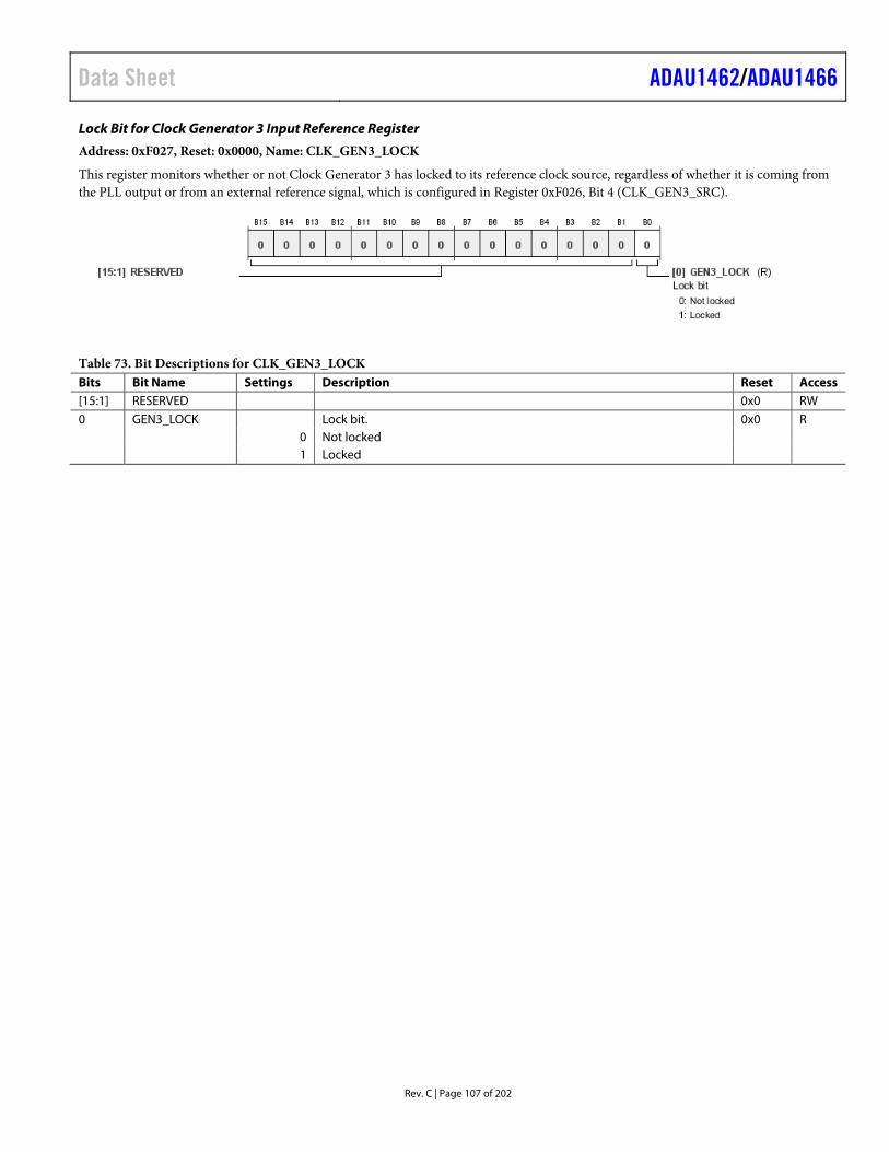
Data Sheet ADAU1462/ADAU1466
Rev. C | Page 107 of 202
Lock Bit for Clock Generator 3 Input Reference Register
Address: 0xF027, Reset: 0x0000, Name: CLK_GEN3_LOCK
This register monitors whether or not Clock Generator 3 has locked to its reference clock source, regardless of whether it is coming from the PLL output or from an external reference signal, which is configured in Register 0xF026, Bit 4 (CLK_GEN3_SRC).
Table 73. Bit Descriptions for CLK_GEN3_LOCK Bits Bit Name Settings Description Reset Access [15:1] RESERVED 0x0 RW 0 GEN3_LOCK Lock bit. 0x0 R 0 Not locked 1 Locked
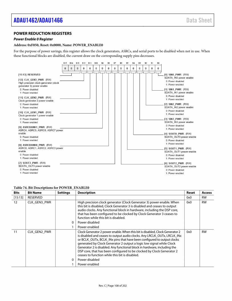
ADAU1462/ADAU1466 Data Sheet
Rev. C | Page 108 of 202
POWER REDUCTION REGISTERS Power Enable 0 Register
Address: 0xF050, Reset: 0x0000, Name: POWER_ENABLE0
For the purpose of power savings, this register allows the clock generators, ASRCs, and serial ports to be disabled when not in use. When these functional blocks are disabled, the current draw on the corresponding supply pins decreases.
Table 74. Bit Descriptions for POWER_ENABLE0 Bits Bit Name Settings Description Reset Access [15:13] RESERVED 0x0 RW 12 CLK_GEN3_PWR High precision clock generator (Clock Generator 3) power enable. When
this bit is disabled, Clock Generator 3 is disabled and ceases to output audio clocks. Any functional block in hardware, including the DSP core, that has been configured to be clocked by Clock Generator 3 ceases to function while this bit is disabled.
0x0 RW
0 Power disabled 1 Power enabled 11 CLK_GEN2_PWR Clock Generator 2 power enable. When this bit is disabled, Clock Generator 2
is disabled and ceases to output audio clocks. Any LRCLK_OUTx, LRCLK_INx or BCLK_OUTx, BCLK_INx pins that have been configured to output clocks generated by Clock Generator 2 output a logic low signal while Clock Generator 2 is disabled. Any functional block in hardware, including the DSP core, that has been configured to be clocked by Clock Generator 2 ceases to function while this bit is disabled.
0x0 RW
0 Power disabled 1 Power enabled
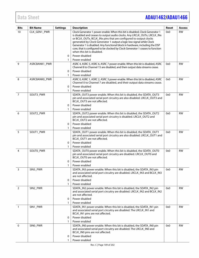
Data Sheet ADAU1462/ADAU1466
Rev. C | Page 109 of 202
Bits Bit Name Settings Description Reset Access 10 CLK_GEN1_PWR Clock Generator 1 power enable. When this bit is disabled, Clock Generator 1
is disabled and ceases to output audio clocks. Any LRCLK_OUTx, LRCLK_INx or BCLK_OUTx, BCLK_INx pins that are configured to output clocks generated by Clock Generator 1 output a logic low signal while Clock Generator 1 is disabled. Any functional block in hardware, including the DSP core, that is configured to be clocked by Clock Generator 1 ceases to function when this bit is disabled.
0x0 RW
0 Power disabled 1 Power enabled 9 ASRCBANK1_PWR ASRC 4, ASRC 5, ASRC 6, ASRC 7 power enable. When this bit is disabled, ASRC
Channel 8 to Channel 15 are disabled, and their output data streams cease. 0x0 RW
0 Power disabled 1 Power enabled 8 ASRCBANK0_PWR ASRC 0, ASRC 1, ASRC 2, ASRC 3 power enable. When this bit is disabled, ASRC
Channel 0 to Channel 7 are disabled, and their output data streams cease. 0x0 RW
0 Power disabled 1 Power enabled 7 SOUT3_PWR SDATA_OUT3 power enable. When this bit is disabled, the SDATA_OUT3
pin and associated serial port circuitry are also disabled. LRCLK_OUT3 and BCLK_OUT3 are not affected.
0x0 RW
0 Power disabled 1 Power enabled 6 SOUT2_PWR SDATA_OUT2 power enable. When this bit is disabled, the SDATA_OUT2
pin and associated serial port circuitry is disabled. LRCLK_OUT2 and BCLK_OUT2 are not affected.
0x0 RW
0 Power disabled 1 Power enabled 5 SOUT1_PWR SDATA_OUT1 power enable. When this bit is disabled, the SDATA_OUT1
pin and associated serial port circuitry are also disabled. LRCLK_OUT1 and BCLK_OUT1 are not affected.
0x0 RW
0 Power disabled 1 Power enabled 4 SOUT0_PWR SDATA_OUT0 power enable. When this bit is disabled, the SDATA_OUT0
pin and associated serial port circuitry are disabled. LRCLK_OUT0 and BCLK_OUT0 are not affected.
0x0 RW
0 Power disabled 1 Power enabled 3 SIN3_PWR SDATA_IN3 power enable. When this bit is disabled, the SDATA_IN3 pin
and associated serial port circuitry are disabled. LRCLK_IN3 and BCLK_IN3 are not affected.
0x0 RW
0 Power disabled 1 Power enabled 2 SIN2_PWR SDATA_IN2 power enable. When this bit is disabled, the SDATA_IN2 pin
and associated serial port circuitry are disabled. LRCLK_IN2 and BCLK_IN2 are not affected.
0x0 RW
0 Power disabled 1 Power enabled 1 SIN1_PWR SDATA_IN1 power enable. When this bit is disabled, the SDATA_IN1 pin
and associated serial port circuitry are disabled. The LRCLK_IN1 and BCLK_IN1 pins are not affected.
0x0 RW
0 Power disabled 1 Power enabled 0 SIN0_PWR SDATA_IN0 power enable. When this bit is disabled, the SDATA_IN0 pin
and associated serial port circuitry are disabled. The LRCLK_IN0 and BCLK_IN0 pins are not affected.
0x0 RW
0 Power disabled 1 Power enabled
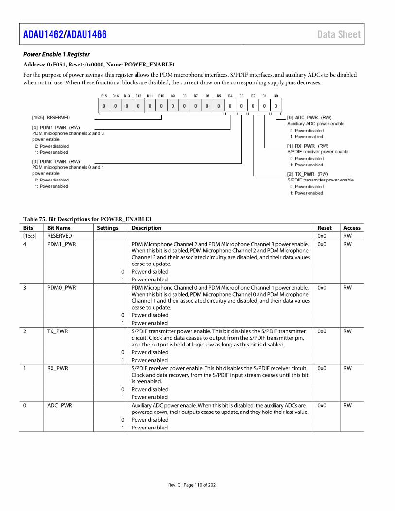
ADAU1462/ADAU1466 Data Sheet
Rev. C | Page 110 of 202
Power Enable 1 Register
Address: 0xF051, Reset: 0x0000, Name: POWER_ENABLE1
For the purpose of power savings, this register allows the PDM microphone interfaces, S/PDIF interfaces, and auxiliary ADCs to be disabled when not in use. When these functional blocks are disabled, the current draw on the corresponding supply pins decreases.
Table 75. Bit Descriptions for POWER_ENABLE1 Bits Bit Name Settings Description Reset Access [15:5] RESERVED 0x0 RW 4 PDM1_PWR PDM Microphone Channel 2 and PDM Microphone Channel 3 power enable.
When this bit is disabled, PDM Microphone Channel 2 and PDM Microphone Channel 3 and their associated circuitry are disabled, and their data values cease to update.
0x0 RW
0 Power disabled 1 Power enabled 3 PDM0_PWR PDM Microphone Channel 0 and PDM Microphone Channel 1 power enable.
When this bit is disabled, PDM Microphone Channel 0 and PDM Microphone Channel 1 and their associated circuitry are disabled, and their data values cease to update.
0x0 RW
0 Power disabled 1 Power enabled 2 TX_PWR S/PDIF transmitter power enable. This bit disables the S/PDIF transmitter
circuit. Clock and data ceases to output from the S/PDIF transmitter pin, and the output is held at logic low as long as this bit is disabled.
0x0 RW
0 Power disabled 1 Power enabled 1 RX_PWR S/PDIF receiver power enable. This bit disables the S/PDIF receiver circuit.
Clock and data recovery from the S/PDIF input stream ceases until this bit is reenabled.
0x0 RW
0 Power disabled 1 Power enabled 0 ADC_PWR Auxiliary ADC power enable. When this bit is disabled, the auxiliary ADCs are
powered down, their outputs cease to update, and they hold their last value. 0x0 RW
0 Power disabled 1 Power enabled
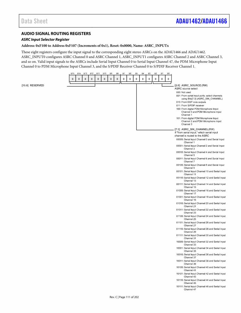
Data Sheet ADAU1462/ADAU1466
Rev. C | Page 111 of 202
AUDIO SIGNAL ROUTING REGISTERS ASRC Input Selector Register
Address: 0xF100 to Address 0xF107 (Increments of 0x1), Reset: 0x0000, Name: ASRC_INPUTx
These eight registers configure the input signal to the corresponding eight stereo ASRCs on the ADAU1466 and ADAU1462. ASRC_INPUT0 configures ASRC Channel 0 and ASRC Channel 1, ASRC_INPUT1 configures ASRC Channel 2 and ASRC Channel 3, and so on. Valid input signals to the ASRCs include Serial Input Channel 0 to Serial Input Channel 47, the PDM Microphone Input Channel 0 to PDM Microphone Input Channel 3, and the S/PDIF Receiver Channel 0 to S/PDIF Receiver Channel 1.
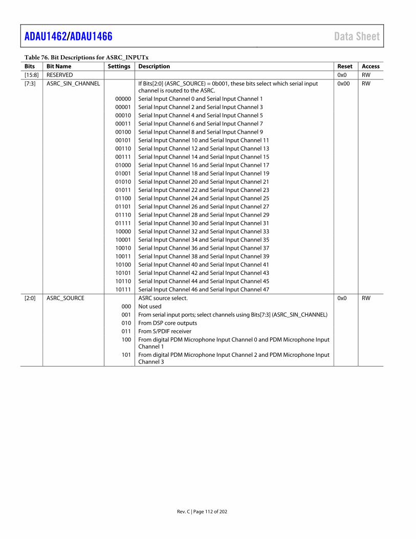
ADAU1462/ADAU1466 Data Sheet
Rev. C | Page 112 of 202
Table 76. Bit Descriptions for ASRC_INPUTx Bits Bit Name Settings Description Reset Access [15:8] RESERVED 0x0 RW [7:3] ASRC_SIN_CHANNEL If Bits[2:0] (ASRC_SOURCE) = 0b001, these bits select which serial input
channel is routed to the ASRC. 0x00 RW
00000 Serial Input Channel 0 and Serial Input Channel 1 00001 Serial Input Channel 2 and Serial Input Channel 3 00010 Serial Input Channel 4 and Serial Input Channel 5 00011 Serial Input Channel 6 and Serial Input Channel 7 00100 Serial Input Channel 8 and Serial Input Channel 9 00101 Serial Input Channel 10 and Serial Input Channel 11 00110 Serial Input Channel 12 and Serial Input Channel 13 00111 Serial Input Channel 14 and Serial Input Channel 15 01000 Serial Input Channel 16 and Serial Input Channel 17 01001 Serial Input Channel 18 and Serial Input Channel 19 01010 Serial Input Channel 20 and Serial Input Channel 21 01011 Serial Input Channel 22 and Serial Input Channel 23 01100 Serial Input Channel 24 and Serial Input Channel 25 01101 Serial Input Channel 26 and Serial Input Channel 27 01110 Serial Input Channel 28 and Serial Input Channel 29 01111 Serial Input Channel 30 and Serial Input Channel 31 10000 Serial Input Channel 32 and Serial Input Channel 33 10001 Serial Input Channel 34 and Serial Input Channel 35 10010 Serial Input Channel 36 and Serial Input Channel 37 10011 Serial Input Channel 38 and Serial Input Channel 39 10100 Serial Input Channel 40 and Serial Input Channel 41 10101 Serial Input Channel 42 and Serial Input Channel 43 10110 Serial Input Channel 44 and Serial Input Channel 45 10111 Serial Input Channel 46 and Serial Input Channel 47 [2:0] ASRC_SOURCE ASRC source select. 0x0 RW 000 Not used 001 From serial input ports; select channels using Bits[7:3] (ASRC_SIN_CHANNEL) 010 From DSP core outputs 011 From S/PDIF receiver 100 From digital PDM Microphone Input Channel 0 and PDM Microphone Input
Channel 1
101 From digital PDM Microphone Input Channel 2 and PDM Microphone Input Channel 3
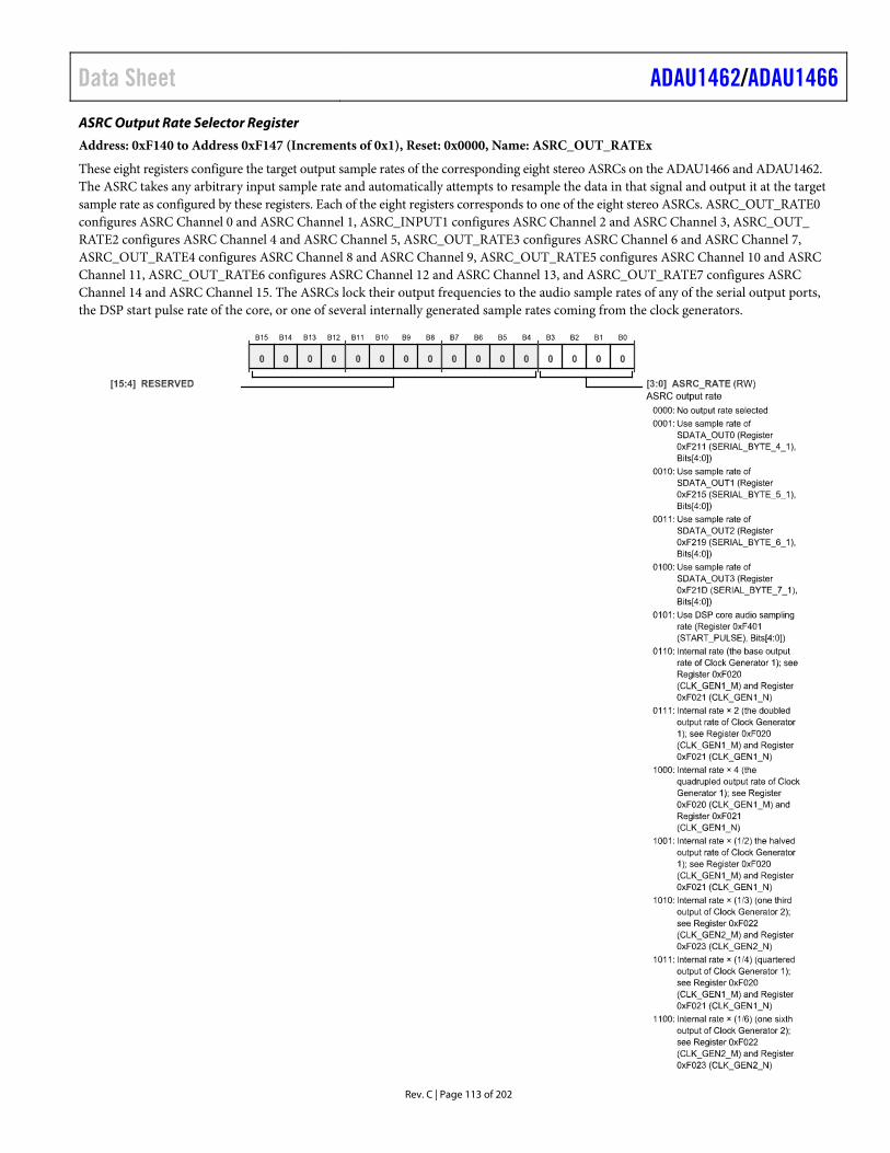
Data Sheet ADAU1462/ADAU1466
Rev. C | Page 113 of 202
ASRC Output Rate Selector Register
Address: 0xF140 to Address 0xF147 (Increments of 0x1), Reset: 0x0000, Name: ASRC_OUT_RATEx
These eight registers configure the target output sample rates of the corresponding eight stereo ASRCs on the ADAU1466 and ADAU1462. The ASRC takes any arbitrary input sample rate and automatically attempts to resample the data in that signal and output it at the target sample rate as configured by these registers. Each of the eight registers corresponds to one of the eight stereo ASRCs. ASRC_OUT_RATE0 configures ASRC Channel 0 and ASRC Channel 1, ASRC_INPUT1 configures ASRC Channel 2 and ASRC Channel 3, ASRC_OUT_ RATE2 configures ASRC Channel 4 and ASRC Channel 5, ASRC_OUT_RATE3 configures ASRC Channel 6 and ASRC Channel 7, ASRC_OUT_RATE4 configures ASRC Channel 8 and ASRC Channel 9, ASRC_OUT_RATE5 configures ASRC Channel 10 and ASRC Channel 11, ASRC_OUT_RATE6 configures ASRC Channel 12 and ASRC Channel 13, and ASRC_OUT_RATE7 configures ASRC Channel 14 and ASRC Channel 15. The ASRCs lock their output frequencies to the audio sample rates of any of the serial output ports, the DSP start pulse rate of the core, or one of several internally generated sample rates coming from the clock generators.
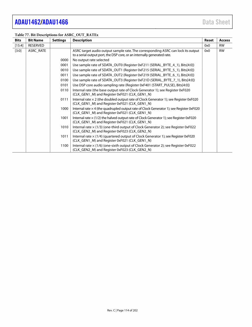
ADAU1462/ADAU1466 Data Sheet
Rev. C | Page 114 of 202
Table 77. Bit Descriptions for ASRC_OUT_RATEx Bits Bit Name Settings Description Reset Access [15:4] RESERVED 0x0 RW [3:0] ASRC_RATE ASRC target audio output sample rate. The corresponding ASRC can lock its output
to a serial output port, the DSP core, or an internally generated rate. 0x0 RW
0000 No output rate selected 0001 Use sample rate of SDATA_OUT0 (Register 0xF211 (SERIAL_BYTE_4_1), Bits[4:0]) 0010 Use sample rate of SDATA_OUT1 (Register 0xF215 (SERIAL_BYTE_5_1), Bits[4:0]) 0011 Use sample rate of SDATA_OUT2 (Register 0xF219 (SERIAL_BYTE_6_1), Bits[4:0]) 0100 Use sample rate of SDATA_OUT3 (Register 0xF21D (SERIAL_BYTE_7_1), Bits[4:0]) 0101 Use DSP core audio sampling rate (Register 0xF401 (START_PULSE), Bits[4:0]) 0110 Internal rate (the base output rate of Clock Generator 1); see Register 0xF020
(CLK_GEN1_M) and Register 0xF021 (CLK_GEN1_N)
0111 Internal rate × 2 (the doubled output rate of Clock Generator 1); see Register 0xF020 (CLK_GEN1_M) and Register 0xF021 (CLK_GEN1_N)
1000 Internal rate × 4 (the quadrupled output rate of Clock Generator 1); see Register 0xF020 (CLK_GEN1_M) and Register 0xF021 (CLK_GEN1_N)
1001 Internal rate × (1/2) the halved output rate of Clock Generator 1); see Register 0xF020 (CLK_GEN1_M) and Register 0xF021 (CLK_GEN1_N)
1010 Internal rate × (1/3) (one-third output of Clock Generator 2); see Register 0xF022 (CLK_GEN2_M) and Register 0xF023 (CLK_GEN2_N)
1011 Internal rate × (1/4) (quartered output of Clock Generator 1); see Register 0xF020 (CLK_GEN1_M) and Register 0xF021 (CLK_GEN1_N)
1100 Internal rate × (1/6) (one-sixth output of Clock Generator 2); see Register 0xF022 (CLK_GEN2_M) and Register 0xF023 (CLK_GEN2_N)
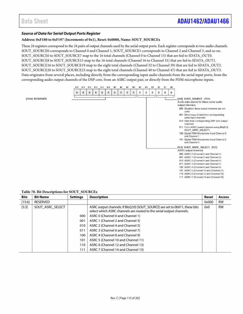
Data Sheet ADAU1462/ADAU1466
Rev. C | Page 115 of 202
Source of Data for Serial Output Ports Register
Address: 0xF180 to 0xF197 (Increments of 0x1), Reset: 0x0000, Name: SOUT_SOURCEx
These 24 registers correspond to the 24 pairs of output channels used by the serial output ports. Each register corresponds to two audio channels. SOUT_SOURCE0 corresponds to Channel 0 and Channel 1, SOUT_SOURCE1 corresponds to Channel 2 and Channel 3, and so on. SOUT_SOURCE0 to SOUT_SOURCE7 map to the 16 total channels (Channel 0 to Channel 15) that are fed to SDATA_OUT0. SOUT_SOURCE8 to SOUT_SOURCE15 map to the 16 total channels (Channel 16 to Channel 31) that are fed to SDATA_OUT1. SOUT_SOURCE16 to SOUT_SOURCE19 map to the eight total channels (Channel 32 to Channel 39) that are fed to SDATA_OUT2. SOUT_SOURCE20 to SOUT_SOURCE23 map to the eight total channels (Channel 40 to Channel 47) that are fed to SDATA_OUT3. Data originates from several places, including directly from the corresponding input audio channels from the serial input ports, from the corresponding audio output channels of the DSP core, from an ASRC output pair, or directly from the PDM microphone inputs.
Table 78. Bit Descriptions for SOUT_SOURCEx Bits Bit Name Settings Description Reset Access [15:6] RESERVED 0x000 RW [5:3] SOUT_ASRC_SELECT ASRC output channels. If Bits[2:0] (SOUT_SOURCE) are set to 0b011, these bits
select which ASRC channels are routed to the serial output channels. 0x0 RW
000 ASRC 0 (Channel 0 and Channel 1) 001 ASRC 1 (Channel 2 and Channel 3) 010 ASRC 2 (Channel 4 and Channel 5) 011 ASRC 3 (Channel 6 and Channel 7) 100 ASRC 4 (Channel 8 and Channel 9) 101 ASRC 5 (Channel 10 and Channel 11) 110 ASRC 6 (Channel 12 and Channel 13) 111 ASRC 7 (Channel 14 and Channel 15)
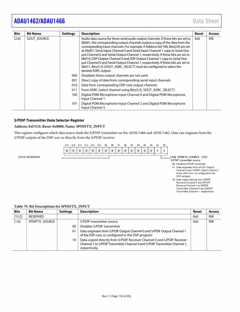
ADAU1462/ADAU1466 Data Sheet
Rev. C | Page 116 of 202
Bits Bit Name Settings Description Reset Access [2:0] SOUT_SOURCE Audio data source for these serial audio output channels. If these bits are set to
0b001, the corresponding output channels output a copy of the data from the corresponding input channels. For example, if Address 0xF180, Bits[2:0] are set to 0b001, Serial Input Channel 0 and Serial Input Channel 1 copy to Serial Out-put Channel 0 and Serial Output Channel 1, respectively. If these bits are set to 0b010, DSP Output Channel 0 and DSP Output Channel 1 copy to Serial Out-put Channel 0 and Serial Output Channel 1, respectively. If these bits are set to 0b011, Bits[5:3] (SOUT_ASRC_SELECT) must be configured to select the desired ASRC output.
0x0 RW
000 Disabled; these output channels are not used 001 Direct copy of data from corresponding serial input channels 010 Data from corresponding DSP core output channels 011 From ASRC (select channel using Bits[5:3], SOUT_ASRC_SELECT) 100 Digital PDM Microphone Input Channel 0 and Digital PDM Microphone
Input Channel 1
101 Digital PDM Microphone Input Channel 2 and Digital PDM Microphone Input Channel 3
S/PDIF Transmitter Data Selector Register
Address: 0xF1C0, Reset: 0x0000, Name: SPDIFTX_INPUT
This register configures which data source feeds the S/PDIF transmitter on the ADAU1466 and ADAU1462. Data can originate from the S/PDIF outputs of the DSP core or directly from the S/PDIF receiver.
Table 79. Bit Descriptions for SPDIFTX_INPUT Bits Bit Name Settings Description Reset Access [15:2] RESERVED 0x0 RW [1:0] SPDIFTX_SOURCE S/PDIF transmitter source. 0x0 RW 00 Disables S/PDIF transmitter 01 Data originates from S/PDIF Output Channel 0 and S/PDIF Output Channel 1
of the DSP core, as configured in the DSP program
10 Data copied directly from S/PDIF Receiver Channel 0 and S/PDIF Receiver Channel 1 to S/PDIF Transmitter Channel 0 and S/PDIF Transmitter Channel 1, respectively
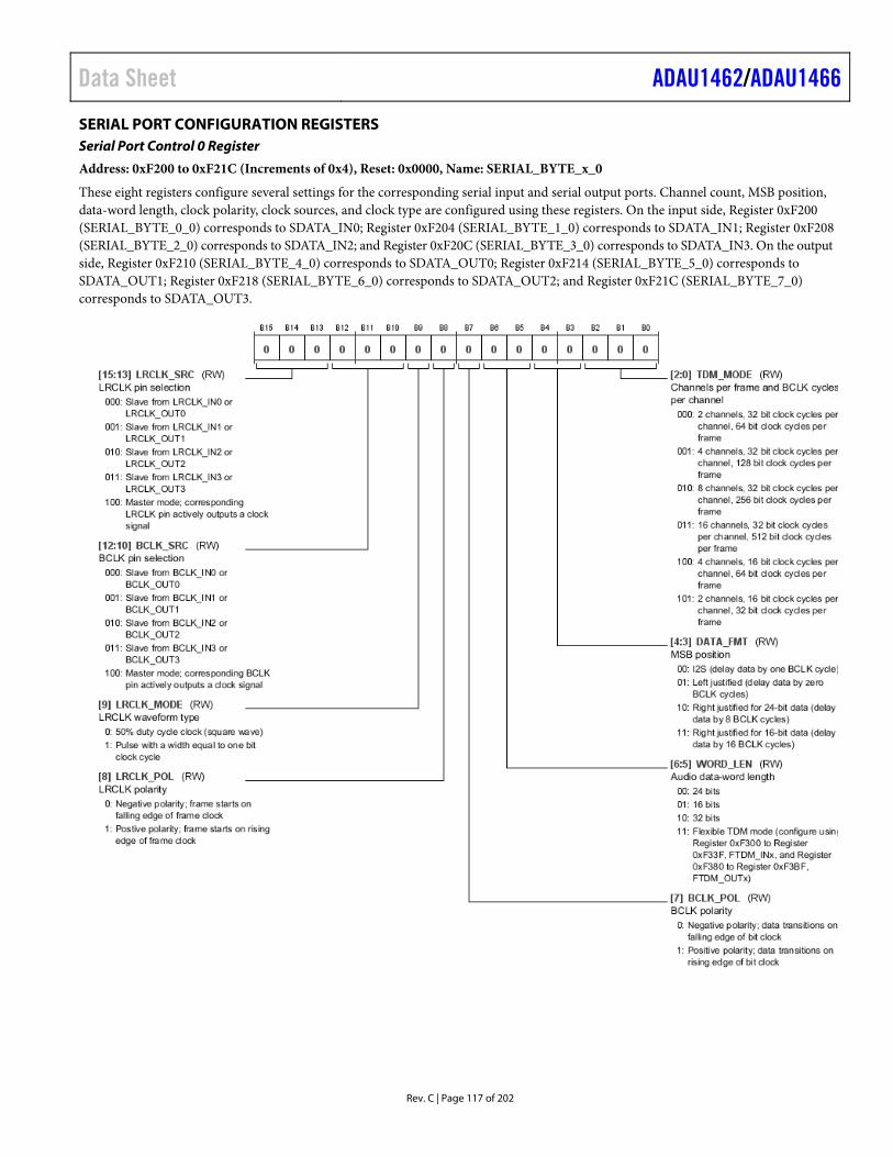
Data Sheet ADAU1462/ADAU1466
Rev. C | Page 117 of 202
SERIAL PORT CONFIGURATION REGISTERS Serial Port Control 0 Register
Address: 0xF200 to 0xF21C (Increments of 0x4), Reset: 0x0000, Name: SERIAL_BYTE_x_0
These eight registers configure several settings for the corresponding serial input and serial output ports. Channel count, MSB position, data-word length, clock polarity, clock sources, and clock type are configured using these registers. On the input side, Register 0xF200 (SERIAL_BYTE_0_0) corresponds to SDATA_IN0; Register 0xF204 (SERIAL_BYTE_1_0) corresponds to SDATA_IN1; Register 0xF208 (SERIAL_BYTE_2_0) corresponds to SDATA_IN2; and Register 0xF20C (SERIAL_BYTE_3_0) corresponds to SDATA_IN3. On the output side, Register 0xF210 (SERIAL_BYTE_4_0) corresponds to SDATA_OUT0; Register 0xF214 (SERIAL_BYTE_5_0) corresponds to SDATA_OUT1; Register 0xF218 (SERIAL_BYTE_6_0) corresponds to SDATA_OUT2; and Register 0xF21C (SERIAL_BYTE_7_0) corresponds to SDATA_OUT3.
ADAU1462/ADAU1466 Data Sheet
Rev. C | Page 118 of 202
Table 80. Bit Descriptions for SERIAL_BYTE_x_0 Bits Bit Name Settings Description Reset Access [15:13] LRCLK_SRC LRCLK pin selection. These bits configure whether the corresponding
serial port is a frame clock master or slave. When configured as a master, the corresponding LRCLK pin (LRCLK_INx for SDATA_INx pins and LRCLK_OUTx for SDATA_OUTx pins) with the same number as the serial port (for example, LRCLK_OUT0 for SDATA_OUT0) actively drives out a clock signal. When configured as a slave, the serial port can receive its clock signal from any of the four corresponding LRCLK pins (LRCLK_INx pins for SDATA_INx pins or LRCLK_OUTx pins for SDATA_OUTx pins).
0x0 RW
000 Slave from LRCLK_IN0 or LRCLK_OUT0 001 Slave from LRCLK_IN1 or LRCLK_OUT1 010 Slave from LRCLK_IN2 or LRCLK_OUT2 011 Slave from LRCLK_IN3 or LRCLK_OUT3 100 Master mode; corresponding LRCLK pin actively outputs a clock signal [12:10] BCLK_SRC BCLK pin selection. These bits configure whether the corresponding serial
port is a bit clock master or slave. When configured as a master, the corresponding BCLK pin (BCLK_INx for SDATA_INx pins and BCLK_OUTx for SDATA_OUTx pins) with the same number as the serial port (for example, BCLK_OUT0 for SDATA_OUT0) actively drives out a clock signal. When configured as a slave, the serial port can receive its clock signal from any of the four corresponding BCLK pins (BCLK_INx pins for SDATA_INx pins or BCLK_OUTx pins for SDATA_OUTx pins).
0x0 RW
000 Slave from BCLK_IN0 or BCLK_OUT0 001 Slave from BCLK_IN1 or BCLK_OUT1 010 Slave from BCLK_IN2 or BCLK_OUT2 011 Slave from BCLK_IN3 or BCLK_OUT3 100 Master mode; corresponding BCLK pin actively outputs a clock signal 9 LRCLK_MODE LRCLK waveform type. The frame clock can be a 50/50 duty cycle square
wave or a short pulse. 0x0 RW
0 50% duty cycle clock (square wave) 1 Pulse with a width equal to one bit clock cycle 8 LRCLK_POL LRCLK polarity. This bit sets the frame clock polarity on the corresponding
serial port. Negative polarity means that the frame starts on the falling edge of the frame clock. This conforms to the I2S standard audio format.
0x0 RW
0 Negative polarity; frame starts on falling edge of frame clock 1 Positive polarity; frame starts on rising edge of frame clock 7 BCLK_POL BCLK polarity. This bit sets the bit clock polarity on the corresponding
serial port. Negative polarity means that the data signal transitions on the falling edge of the bit clock. This conforms to the I2S standard audio format.
0x0 RW
0 Negative polarity; data transitions on falling edge of bit clock 1 Positive polarity; data transitions on rising edge of bit clock [6:5] WORD_LEN Audio data-word length. These bits set the word length of the audio data
channels on the corresponding serial port. For serial input ports, if the input data has more words than the length as configured by these bits, the extra data bits are ignored. For output serial ports, if the word length, as configured by these bits, is shorter than the data length coming from the data source (the DSP, ASRCs, S/PDIF receiver, PDM inputs, or serial inputs), the extra data bits are truncated and output as 0s. If Bits[6:5] (WORD_LEN) are set to 0b10 for 32-bit mode, the corresponding 32-bit input or output cells are required in SigmaStudio.
0x0 RW
00 24 bits 01 16 bits 10 32 bits 11 Flexible TDM mode (configure using Register 0xF300 to Register 0xF33F,
FTDM_INx, and Register 0xF380 to Register 0xF3BF, FTDM_OUTx)
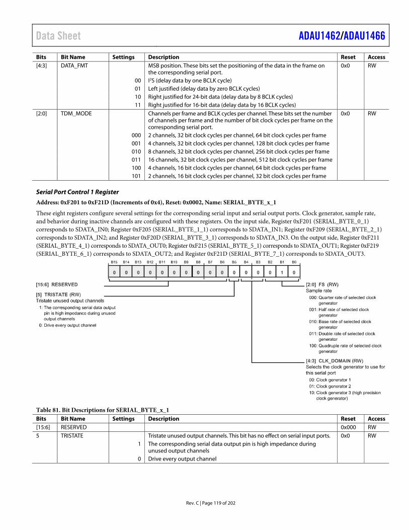
Data Sheet ADAU1462/ADAU1466
Rev. C | Page 119 of 202
Bits Bit Name Settings Description Reset Access [4:3] DATA_FMT MSB position. These bits set the positioning of the data in the frame on
the corresponding serial port. 0x0 RW
00 I2S (delay data by one BCLK cycle) 01 Left justified (delay data by zero BCLK cycles) 10 Right justified for 24-bit data (delay data by 8 BCLK cycles) 11 Right justified for 16-bit data (delay data by 16 BCLK cycles) [2:0] TDM_MODE Channels per frame and BCLK cycles per channel. These bits set the number
of channels per frame and the number of bit clock cycles per frame on the corresponding serial port.
0x0 RW
000 2 channels, 32 bit clock cycles per channel, 64 bit clock cycles per frame 001 4 channels, 32 bit clock cycles per channel, 128 bit clock cycles per frame 010 8 channels, 32 bit clock cycles per channel, 256 bit clock cycles per frame 011 16 channels, 32 bit clock cycles per channel, 512 bit clock cycles per frame 100 4 channels, 16 bit clock cycles per channel, 64 bit clock cycles per frame 101 2 channels, 16 bit clock cycles per channel, 32 bit clock cycles per frame
Serial Port Control 1 Register
Address: 0xF201 to 0xF21D (Increments of 0x4), Reset: 0x0002, Name: SERIAL_BYTE_x_1
These eight registers configure several settings for the corresponding serial input and serial output ports. Clock generator, sample rate, and behavior during inactive channels are configured with these registers. On the input side, Register 0xF201 (SERIAL_BYTE_0_1) corresponds to SDATA_IN0; Register 0xF205 (SERIAL_BYTE_1_1) corresponds to SDATA_IN1; Register 0xF209 (SERIAL_BYTE_2_1) corresponds to SDATA_IN2; and Register 0xF20D (SERIAL_BYTE_3_1) corresponds to SDATA_IN3. On the output side, Register 0xF211 (SERIAL_BYTE_4_1) corresponds to SDATA_OUT0; Register 0xF215 (SERIAL_BYTE_5_1) corresponds to SDATA_OUT1; Register 0xF219 (SERIAL_BYTE_6_1) corresponds to SDATA_OUT2; and Register 0xF21D (SERIAL_BYTE_7_1) corresponds to SDATA_OUT3.
Table 81. Bit Descriptions for SERIAL_BYTE_x_1 Bits Bit Name Settings Description Reset Access [15:6] RESERVED 0x000 RW 5 TRISTATE Tristate unused output channels. This bit has no effect on serial input ports. 0x0 RW 1 The corresponding serial data output pin is high impedance during
unused output channels
0 Drive every output channel
ADAU1462/ADAU1466 Data Sheet
Rev. C | Page 120 of 202
Bits Bit Name Settings Description Reset Access [4:3] CLK_DOMAIN Selects the clock generator to use for the serial port. These bits select the
clock generator to use for this serial port when it is configured as a clock master. This setting is valid only when Bits[15:13] (LRCLK_SRC) of the corresponding SERIAL_BYTE_x_0 register are set to 0b100 (master mode) and Bits[12:10] (BCLK_SRC) are set to 0b100 (master mode).
0x0 RW
00 Clock Generator 1 01 Clock Generator 2 10 Clock Generator 3 (high precision clock generator) [2:0] FS Sample rate. These bits set the sample rate to use for the serial port when
it is configured as a clock master. This setting is valid only when Bits[15:13] (LRCLK_SRC) of the corresponding SERIAL_BYTE_x_0 register are set to 0b100 (master mode) and Bits[12:10] BCLK_SRC are set to 0b100 (master mode). Bits[4:3] (CLK_DOMAIN) select which clock generator to use, and Bits[2:0] (FS) select which of the five clock generator outputs to use.
0x2 RW
000 Quarter rate of selected clock generator 001 Half rate of selected clock generator 010 Base rate of selected clock generator 011 Double rate of selected clock generator 100 Quadruple rate of selected clock generator
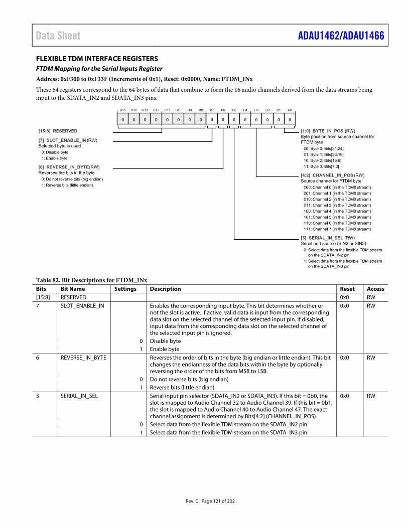
Data Sheet ADAU1462/ADAU1466
Rev. C | Page 121 of 202
FLEXIBLE TDM INTERFACE REGISTERS FTDM Mapping for the Serial Inputs Register
Address: 0xF300 to 0xF33F (Increments of 0x1), Reset: 0x0000, Name: FTDM_INx
These 64 registers correspond to the 64 bytes of data that combine to form the 16 audio channels derived from the data streams being input to the SDATA_IN2 and SDATA_IN3 pins.
Table 82. Bit Descriptions for FTDM_INx Bits Bit Name Settings Description Reset Access [15:8] RESERVED 0x0 RW 7 SLOT_ENABLE_IN Enables the corresponding input byte. This bit determines whether or
not the slot is active. If active, valid data is input from the corresponding data slot on the selected channel of the selected input pin. If disabled, input data from the corresponding data slot on the selected channel of the selected input pin is ignored.
0x0 RW
0 Disable byte 1 Enable byte 6 REVERSE_IN_BYTE Reverses the order of bits in the byte (big endian or little endian). This bit
changes the endianness of the data bits within the byte by optionally reversing the order of the bits from MSB to LSB.
0x0 RW
0 Do not reverse bits (big endian) 1 Reverse bits (little endian) 5 SERIAL_IN_SEL Serial input pin selector (SDATA_IN2 or SDATA_IN3). If this bit = 0b0, the
slot is mapped to Audio Channel 32 to Audio Channel 39. If this bit = 0b1, the slot is mapped to Audio Channel 40 to Audio Channel 47. The exact channel assignment is determined by Bits[4:2] (CHANNEL_IN_POS).
0x0 RW
0 Select data from the flexible TDM stream on the SDATA_IN2 pin 1 Select data from the flexible TDM stream on the SDATA_IN3 pin
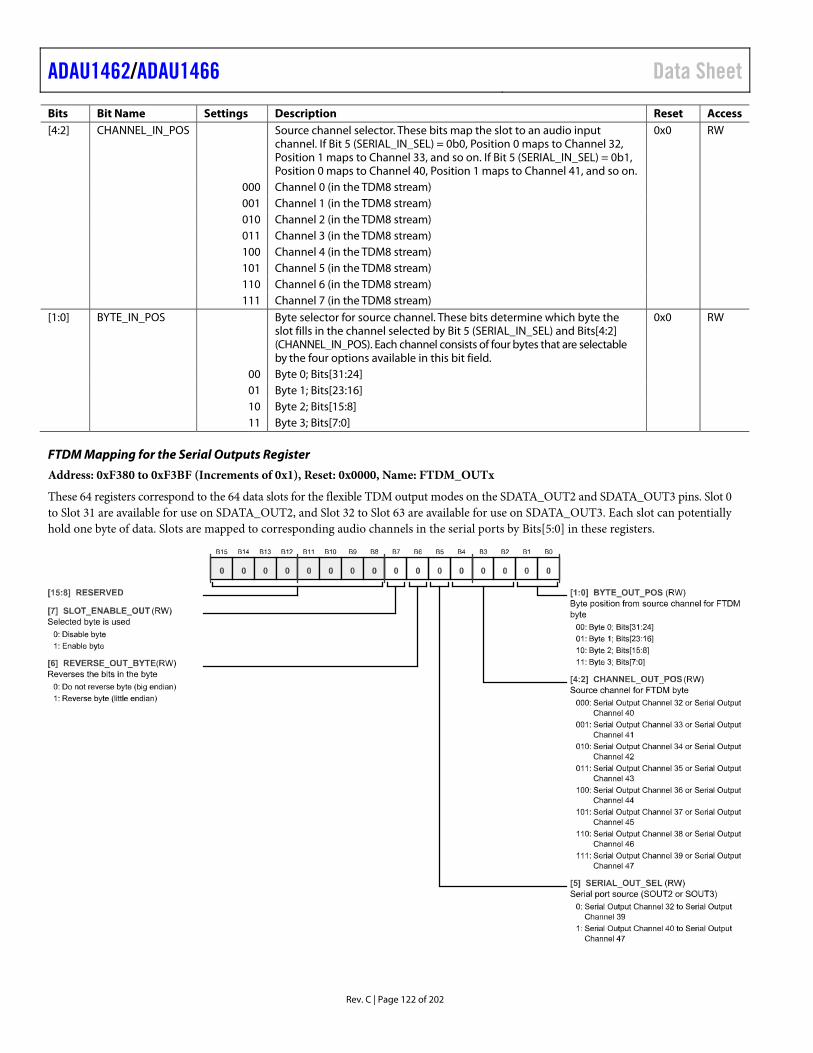
ADAU1462/ADAU1466 Data Sheet
Rev. C | Page 122 of 202
Bits Bit Name Settings Description Reset Access [4:2] CHANNEL_IN_POS Source channel selector. These bits map the slot to an audio input
channel. If Bit 5 (SERIAL_IN_SEL) = 0b0, Position 0 maps to Channel 32, Position 1 maps to Channel 33, and so on. If Bit 5 (SERIAL_IN_SEL) = 0b1, Position 0 maps to Channel 40, Position 1 maps to Channel 41, and so on.
0x0 RW
000 Channel 0 (in the TDM8 stream) 001 Channel 1 (in the TDM8 stream) 010 Channel 2 (in the TDM8 stream) 011 Channel 3 (in the TDM8 stream) 100 Channel 4 (in the TDM8 stream) 101 Channel 5 (in the TDM8 stream) 110 Channel 6 (in the TDM8 stream) 111 Channel 7 (in the TDM8 stream) [1:0] BYTE_IN_POS Byte selector for source channel. These bits determine which byte the
slot fills in the channel selected by Bit 5 (SERIAL_IN_SEL) and Bits[4:2] (CHANNEL_IN_POS). Each channel consists of four bytes that are selectable by the four options available in this bit field.
0x0 RW
00 Byte 0; Bits[31:24] 01 Byte 1; Bits[23:16] 10 Byte 2; Bits[15:8] 11 Byte 3; Bits[7:0]
FTDM Mapping for the Serial Outputs Register
Address: 0xF380 to 0xF3BF (Increments of 0x1), Reset: 0x0000, Name: FTDM_OUTx
These 64 registers correspond to the 64 data slots for the flexible TDM output modes on the SDATA_OUT2 and SDATA_OUT3 pins. Slot 0 to Slot 31 are available for use on SDATA_OUT2, and Slot 32 to Slot 63 are available for use on SDATA_OUT3. Each slot can potentially hold one byte of data. Slots are mapped to corresponding audio channels in the serial ports by Bits[5:0] in these registers.
Data Sheet ADAU1462/ADAU1466
Rev. C | Page 123 of 202
Table 83. Bit Descriptions for FTDM_OUTx Bits Bit Name Settings Description Reset Access [15:8] RESERVED 0x0 RW 7 SLOT_ENABLE_OUT Enables the corresponding output byte. This bit determines whether or
not the slot is active. If Bit 7 (SLOT_ENABLE_OUT) = 0b0 and Bit 5 (TRISTATE) of the corresponding serial output port = 0b1, the corresponding output pin is high impedance during the period in which the corresponding flexible TDM slot is output. If Bit 7 (SLOT_ENABLE_OUT) = 0b0, and Bit 5 (TRISTATE) of the corresponding serial output port = 0b0, the corre-sponding output pin drives logic low during the period in which the corresponding flexible TDM slot is output. If Bit 7 (SLOT_ENABLE_OUT) = 0b1, the corresponding serial output pin outputs valid data during the period in which the corresponding flexible TDM slot is output.
0x0 RW
0 Disable byte 1 Enable byte 6 REVERSE_OUT_BYTE Reverses the bits in the byte (big endian or little endian). This bit changes
the endianness of the data bits within the corresponding flexible TDM slot by optionally reversing the order of the bits from MSB to LSB.
0x0 RW
0 Do not reverse byte (big endian) 1 Reverse byte (little endian) 5 SERIAL_OUT_SEL Source serial output channel group. This bit, together with Bits[4:2]
(CHANNEL_OUT_POS), selects which serial output channel is the source of data for the corresponding flexible TDM output slot.
0x0 RW
0 Serial Output Channel 32 to Serial Output Channel 39 1 Serial Output Channel 40 to Serial Output Channel 47 [4:2] CHANNEL_OUT_POS Source serial output channel. These bits, along with Bit 5 (SERIAL_OUT_SEL),
select which serial output channel is the source of data for the corre-sponding flexible TDM output slot. If Bit 5 (SERIAL_OUT_SEL) = 0b0, Bits[4:2] (CHANNEL_OUT_POS) select serial output channels between Serial Output Channel 32 and Serial Output Channel 39. If Bit 5 (SERIAL_OUT_SEL) = 0b1, Bits[4:2] (CHANNEL_OUT_POS) selects serial output channels between Serial Output Channel 40 and Serial Output Channel 47.
0x0 RW
000 Serial Output Channel 32 or Serial Output Channel 40 001 Serial Output Channel 33 or Serial Output Channel 41 010 Serial Output Channel 34 or Serial Output Channel 42 011 Serial Output Channel 35 or Serial Output Channel 43 100 Serial Output Channel 36 or Serial Output Channel 44 101 Serial Output Channel 37 or Serial Output Channel 45 110 Serial Output Channel 38 or Serial Output Channel 46 111 Serial Output Channel 39 or Serial Output Channel 47 [1:0] BYTE_OUT_POS Source data byte. These bits determine which data byte is used from the
corresponding serial output channel (selected by setting Bit 5 (SERIAL_ OUT_SEL) and Bits[4:2] (CHANNEL_OUT_POS)). Because there can be up to 32 bits in the data-word, four bytes are available.
0x0 RW
00 Byte 0; Bits[31:24] 01 Byte 1; Bits[23:16] 10 Byte 2; Bits[15:8] 11 Byte 3; Bits[7:0]
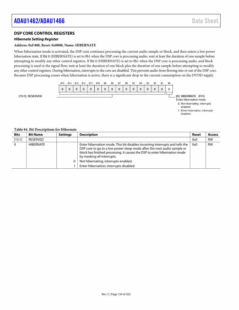
ADAU1462/ADAU1466 Data Sheet
Rev. C | Page 124 of 202
DSP CORE CONTROL REGISTERS Hibernate Setting Register
Address: 0xF400, Reset: 0x0000, Name: HIBERNATE
When hibernation mode is activated, the DSP core continues processing the current audio sample or block, and then enters a low power hibernation state. If Bit 0 (HIBERNATE) is set to 0b1 when the DSP core is processing audio, wait at least the duration of one sample before attempting to modify any other control registers. If Bit 0 (HIBERNATE) is set to 0b1 when the DSP core is processing audio, and block processing is used in the signal flow, wait at least the duration of one block plus the duration of one sample before attempting to modify any other control registers. During hibernation, interrupts to the core are disabled. This prevents audio from flowing into or out of the DSP core. Because DSP processing ceases when hibernation is active, there is a significant drop in the current consumption on the DVDD supply.
Table 84. Bit Descriptions for Hibernate Bits Bit Name Settings Description Reset Access [15:1] RESERVED 0x0 RW 0 HIBERNATE Enter hibernation mode. This bit disables incoming interrupts and tells the
DSP core to go to a low power sleep mode after the next audio sample or block has finished processing. It causes the DSP to enter hibernation mode by masking all interrupts.
0x0 RW
0 Not hibernating; interrupts enabled. 1 Enter hibernation; interrupts disabled.
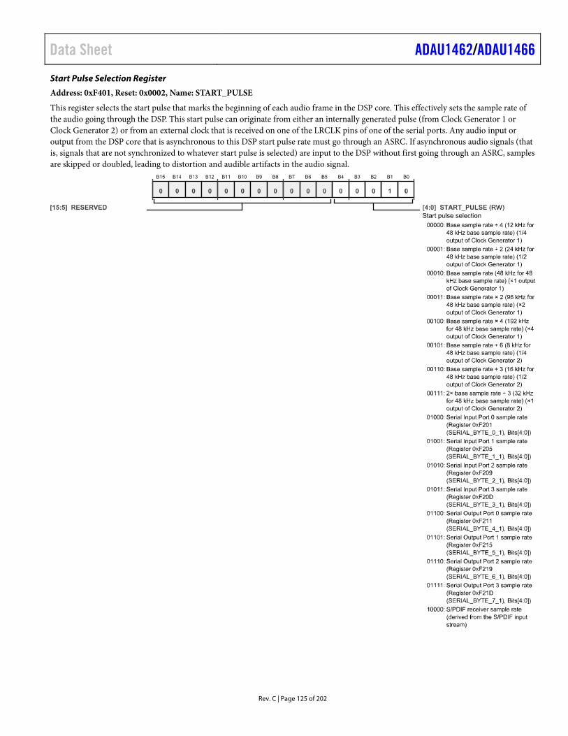
Data Sheet ADAU1462/ADAU1466
Rev. C | Page 125 of 202
Start Pulse Selection Register
Address: 0xF401, Reset: 0x0002, Name: START_PULSE
This register selects the start pulse that marks the beginning of each audio frame in the DSP core. This effectively sets the sample rate of the audio going through the DSP. This start pulse can originate from either an internally generated pulse (from Clock Generator 1 or Clock Generator 2) or from an external clock that is received on one of the LRCLK pins of one of the serial ports. Any audio input or output from the DSP core that is asynchronous to this DSP start pulse rate must go through an ASRC. If asynchronous audio signals (that is, signals that are not synchronized to whatever start pulse is selected) are input to the DSP without first going through an ASRC, samples are skipped or doubled, leading to distortion and audible artifacts in the audio signal.
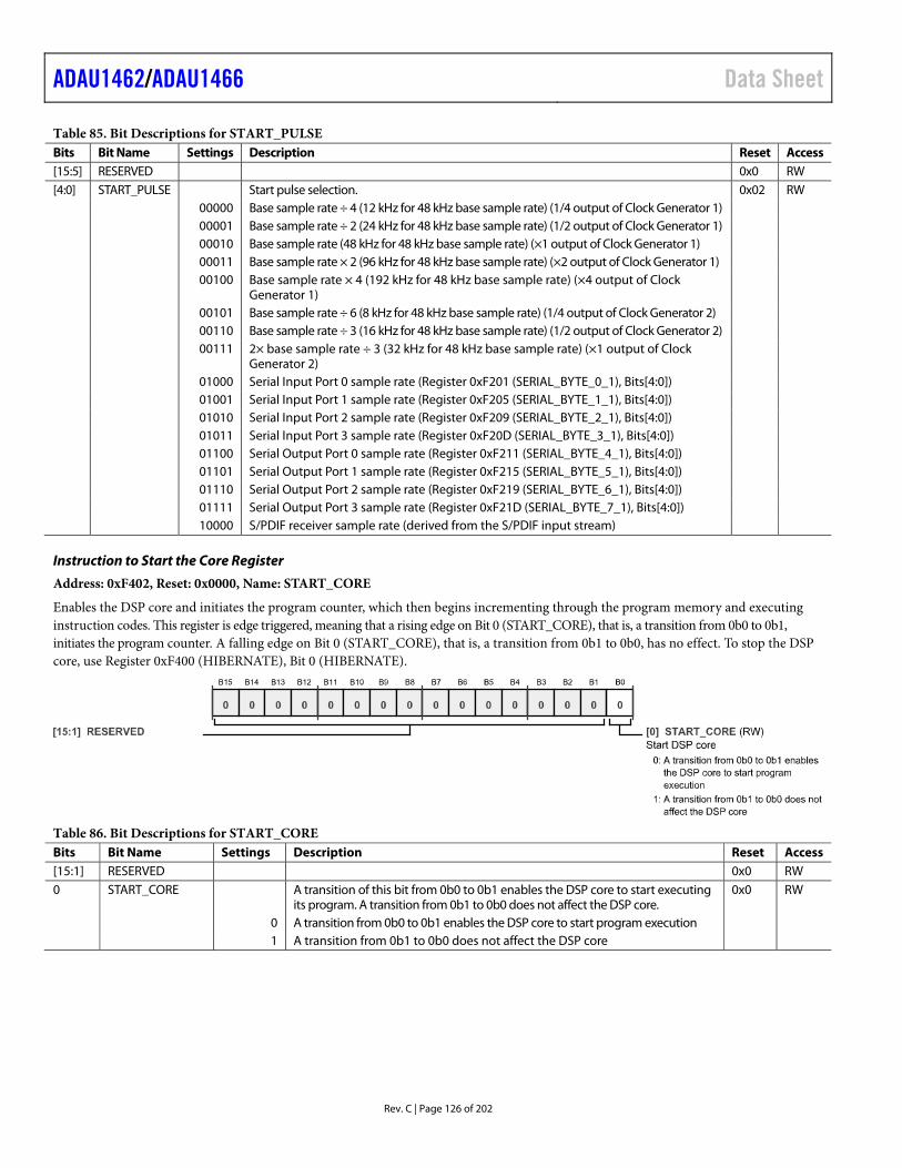
ADAU1462/ADAU1466 Data Sheet
Rev. C | Page 126 of 202
Table 85. Bit Descriptions for START_PULSE Bits Bit Name Settings Description Reset Access [15:5] RESERVED 0x0 RW [4:0] START_PULSE Start pulse selection. 0x02 RW 00000 Base sample rate ÷ 4 (12 kHz for 48 kHz base sample rate) (1/4 output of Clock Generator 1) 00001 Base sample rate ÷ 2 (24 kHz for 48 kHz base sample rate) (1/2 output of Clock Generator 1) 00010 Base sample rate (48 kHz for 48 kHz base sample rate) (×1 output of Clock Generator 1) 00011 Base sample rate × 2 (96 kHz for 48 kHz base sample rate) (×2 output of Clock Generator 1) 00100 Base sample rate × 4 (192 kHz for 48 kHz base sample rate) (×4 output of Clock
Generator 1)
00101 Base sample rate ÷ 6 (8 kHz for 48 kHz base sample rate) (1/4 output of Clock Generator 2) 00110 Base sample rate ÷ 3 (16 kHz for 48 kHz base sample rate) (1/2 output of Clock Generator 2) 00111 2× base sample rate ÷ 3 (32 kHz for 48 kHz base sample rate) (×1 output of Clock
Generator 2)
01000 Serial Input Port 0 sample rate (Register 0xF201 (SERIAL_BYTE_0_1), Bits[4:0]) 01001 Serial Input Port 1 sample rate (Register 0xF205 (SERIAL_BYTE_1_1), Bits[4:0]) 01010 Serial Input Port 2 sample rate (Register 0xF209 (SERIAL_BYTE_2_1), Bits[4:0]) 01011 Serial Input Port 3 sample rate (Register 0xF20D (SERIAL_BYTE_3_1), Bits[4:0]) 01100 Serial Output Port 0 sample rate (Register 0xF211 (SERIAL_BYTE_4_1), Bits[4:0]) 01101 Serial Output Port 1 sample rate (Register 0xF215 (SERIAL_BYTE_5_1), Bits[4:0]) 01110 Serial Output Port 2 sample rate (Register 0xF219 (SERIAL_BYTE_6_1), Bits[4:0]) 01111 Serial Output Port 3 sample rate (Register 0xF21D (SERIAL_BYTE_7_1), Bits[4:0]) 10000 S/PDIF receiver sample rate (derived from the S/PDIF input stream)
Instruction to Start the Core Register
Address: 0xF402, Reset: 0x0000, Name: START_CORE
Enables the DSP core and initiates the program counter, which then begins incrementing through the program memory and executing instruction codes. This register is edge triggered, meaning that a rising edge on Bit 0 (START_CORE), that is, a transition from 0b0 to 0b1, initiates the program counter. A falling edge on Bit 0 (START_CORE), that is, a transition from 0b1 to 0b0, has no effect. To stop the DSP core, use Register 0xF400 (HIBERNATE), Bit 0 (HIBERNATE).
Table 86. Bit Descriptions for START_CORE Bits Bit Name Settings Description Reset Access [15:1] RESERVED 0x0 RW 0 START_CORE A transition of this bit from 0b0 to 0b1 enables the DSP core to start executing
its program. A transition from 0b1 to 0b0 does not affect the DSP core. 0x0 RW
0 A transition from 0b0 to 0b1 enables the DSP core to start program execution 1 A transition from 0b1 to 0b0 does not affect the DSP core
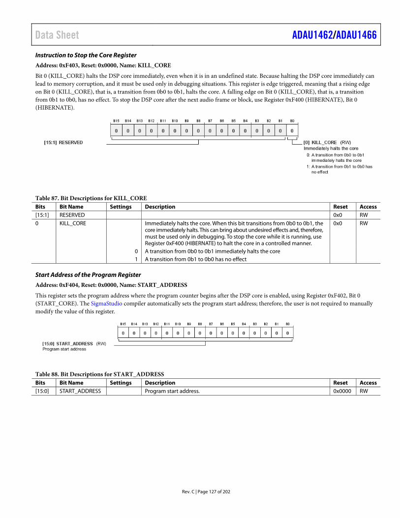
Data Sheet ADAU1462/ADAU1466
Rev. C | Page 127 of 202
Instruction to Stop the Core Register
Address: 0xF403, Reset: 0x0000, Name: KILL_CORE
Bit 0 (KILL_CORE) halts the DSP core immediately, even when it is in an undefined state. Because halting the DSP core immediately can lead to memory corruption, and it must be used only in debugging situations. This register is edge triggered, meaning that a rising edge on Bit 0 (KILL_CORE), that is, a transition from 0b0 to 0b1, halts the core. A falling edge on Bit 0 (KILL_CORE), that is, a transition from 0b1 to 0b0, has no effect. To stop the DSP core after the next audio frame or block, use Register 0xF400 (HIBERNATE), Bit 0 (HIBERNATE).
Table 87. Bit Descriptions for KILL_CORE Bits Bit Name Settings Description Reset Access [15:1] RESERVED 0x0 RW 0 KILL_CORE Immediately halts the core. When this bit transitions from 0b0 to 0b1, the
core immediately halts. This can bring about undesired effects and, therefore, must be used only in debugging. To stop the core while it is running, use Register 0xF400 (HIBERNATE) to halt the core in a controlled manner.
0x0 RW
0 A transition from 0b0 to 0b1 immediately halts the core 1 A transition from 0b1 to 0b0 has no effect
Start Address of the Program Register
Address: 0xF404, Reset: 0x0000, Name: START_ADDRESS
This register sets the program address where the program counter begins after the DSP core is enabled, using Register 0xF402, Bit 0 (START_CORE). The SigmaStudio compiler automatically sets the program start address; therefore, the user is not required to manually modify the value of this register.
Table 88. Bit Descriptions for START_ADDRESS Bits Bit Name Settings Description Reset Access [15:0] START_ADDRESS Program start address. 0x0000 RW
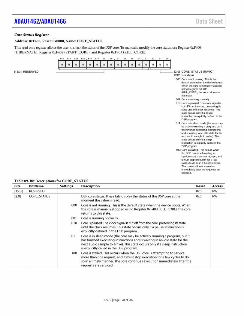
ADAU1462/ADAU1466 Data Sheet
Rev. C | Page 128 of 202
Core Status Register
Address: 0xF405, Reset: 0x0000, Name: CORE_STATUS
This read only register allows the user to check the status of the DSP core. To manually modify the core status, use Register 0xF400 (HIBERNATE), Register 0xF402 (START_CORE), and Register 0xF403 (KILL_CORE).
Table 89. Bit Descriptions for CORE_STATUS Bits Bit Name Settings Description Reset Access [15:3] RESERVED 0x0 RW [2:0] CORE_STATUS DSP core status. These bits display the status of the DSP core at the
moment the value is read. 0x0 RW
000 Core is not running. This is the default state when the device boots. When the core is manually stopped using Register 0xF403 (KILL_CORE), the core returns to this state.
001 Core is running normally. 010 Core is paused. The clock signal is cut off from the core, preserving its state
until the clock resumes. This state occurs only if a pause instruction is explicitly defined in the DSP program.
011 Core is in sleep mode (the core may be actively running a program, but it has finished executing instructions and is waiting in an idle state for the next audio sample to arrive). This state occurs only if a sleep instruction is explicitly called in the DSP program.
100 Core is stalled. This occurs when the DSP core is attempting to service more than one request, and it must stop execution for a few cycles to do so in a timely manner. The core continues execution immediately after the requests are serviced.
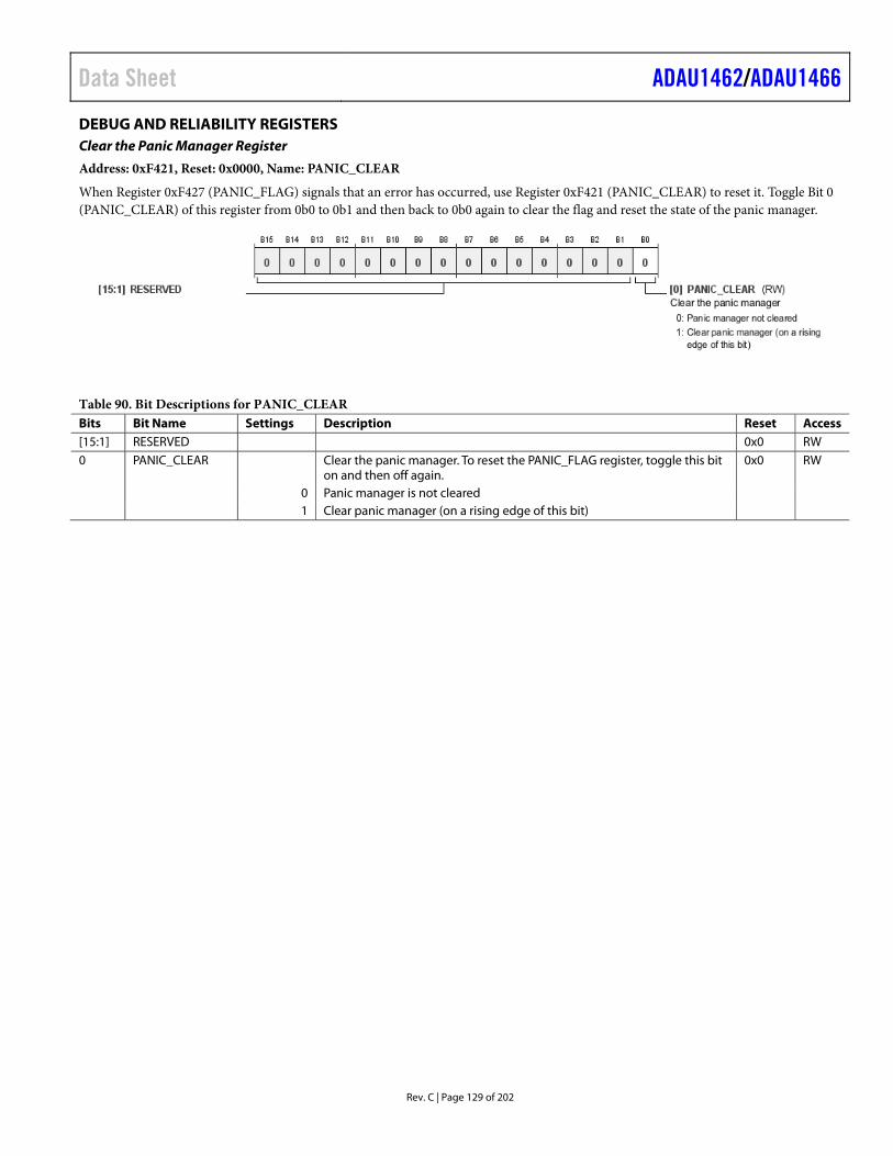
Data Sheet ADAU1462/ADAU1466
Rev. C | Page 129 of 202
DEBUG AND RELIABILITY REGISTERS Clear the Panic Manager Register
Address: 0xF421, Reset: 0x0000, Name: PANIC_CLEAR
When Register 0xF427 (PANIC_FLAG) signals that an error has occurred, use Register 0xF421 (PANIC_CLEAR) to reset it. Toggle Bit 0 (PANIC_CLEAR) of this register from 0b0 to 0b1 and then back to 0b0 again to clear the flag and reset the state of the panic manager.
Table 90. Bit Descriptions for PANIC_CLEAR Bits Bit Name Settings Description Reset Access [15:1] RESERVED 0x0 RW 0 PANIC_CLEAR Clear the panic manager. To reset the PANIC_FLAG register, toggle this bit
on and then off again. 0x0 RW
0 Panic manager is not cleared 1 Clear panic manager (on a rising edge of this bit)
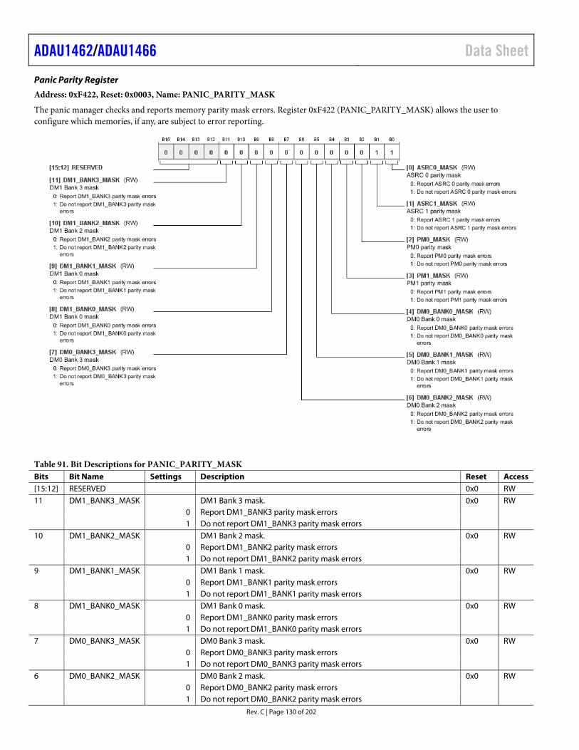
ADAU1462/ADAU1466 Data Sheet
Rev. C | Page 130 of 202
Panic Parity Register
Address: 0xF422, Reset: 0x0003, Name: PANIC_PARITY_MASK
The panic manager checks and reports memory parity mask errors. Register 0xF422 (PANIC_PARITY_MASK) allows the user to configure which memories, if any, are subject to error reporting.
Table 91. Bit Descriptions for PANIC_PARITY_MASK Bits Bit Name Settings Description Reset Access [15:12] RESERVED 0x0 RW 11 DM1_BANK3_MASK DM1 Bank 3 mask. 0x0 RW 0 Report DM1_BANK3 parity mask errors 1 Do not report DM1_BANK3 parity mask errors 10 DM1_BANK2_MASK DM1 Bank 2 mask. 0x0 RW 0 Report DM1_BANK2 parity mask errors 1 Do not report DM1_BANK2 parity mask errors 9 DM1_BANK1_MASK DM1 Bank 1 mask. 0x0 RW 0 Report DM1_BANK1 parity mask errors 1 Do not report DM1_BANK1 parity mask errors 8 DM1_BANK0_MASK DM1 Bank 0 mask. 0x0 RW 0 Report DM1_BANK0 parity mask errors 1 Do not report DM1_BANK0 parity mask errors 7 DM0_BANK3_MASK DM0 Bank 3 mask. 0x0 RW 0 Report DM0_BANK3 parity mask errors 1 Do not report DM0_BANK3 parity mask errors 6 DM0_BANK2_MASK DM0 Bank 2 mask. 0x0 RW 0 Report DM0_BANK2 parity mask errors 1 Do not report DM0_BANK2 parity mask errors
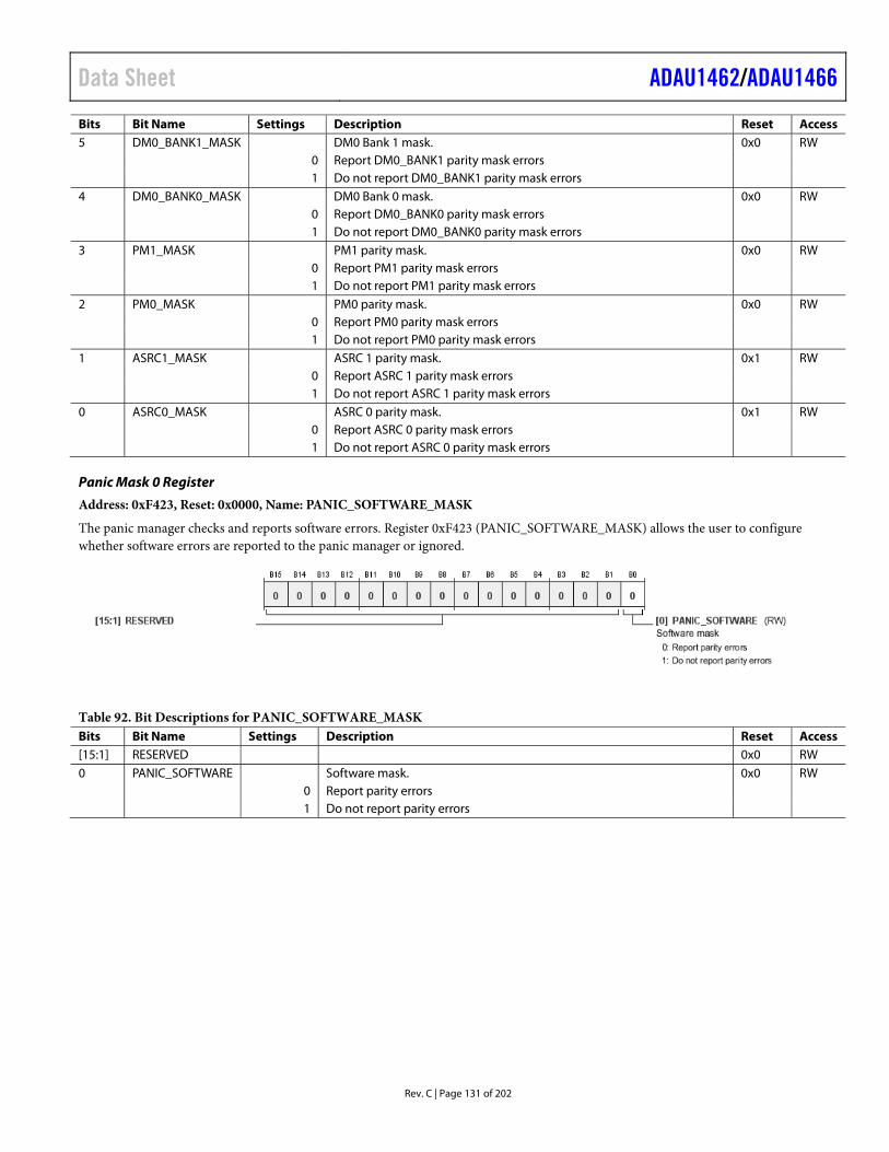
Data Sheet ADAU1462/ADAU1466
Rev. C | Page 131 of 202
Bits Bit Name Settings Description Reset Access 5 DM0_BANK1_MASK DM0 Bank 1 mask. 0x0 RW 0 Report DM0_BANK1 parity mask errors 1 Do not report DM0_BANK1 parity mask errors 4 DM0_BANK0_MASK DM0 Bank 0 mask. 0x0 RW 0 Report DM0_BANK0 parity mask errors 1 Do not report DM0_BANK0 parity mask errors 3 PM1_MASK PM1 parity mask. 0x0 RW 0 Report PM1 parity mask errors 1 Do not report PM1 parity mask errors 2 PM0_MASK PM0 parity mask. 0x0 RW 0 Report PM0 parity mask errors 1 Do not report PM0 parity mask errors 1 ASRC1_MASK ASRC 1 parity mask. 0x1 RW 0 Report ASRC 1 parity mask errors 1 Do not report ASRC 1 parity mask errors 0 ASRC0_MASK ASRC 0 parity mask. 0x1 RW 0 Report ASRC 0 parity mask errors 1 Do not report ASRC 0 parity mask errors
Panic Mask 0 Register
Address: 0xF423, Reset: 0x0000, Name: PANIC_SOFTWARE_MASK
The panic manager checks and reports software errors. Register 0xF423 (PANIC_SOFTWARE_MASK) allows the user to configure whether software errors are reported to the panic manager or ignored.
Table 92. Bit Descriptions for PANIC_SOFTWARE_MASK Bits Bit Name Settings Description Reset Access [15:1] RESERVED 0x0 RW 0 PANIC_SOFTWARE Software mask. 0x0 RW 0 Report parity errors 1 Do not report parity errors
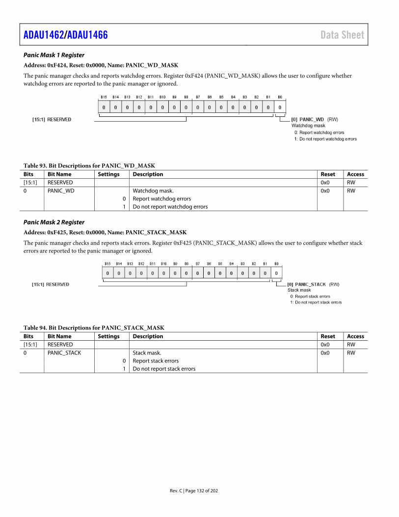
ADAU1462/ADAU1466 Data Sheet
Rev. C | Page 132 of 202
Panic Mask 1 Register
Address: 0xF424, Reset: 0x0000, Name: PANIC_WD_MASK
The panic manager checks and reports watchdog errors. Register 0xF424 (PANIC_WD_MASK) allows the user to configure whether watchdog errors are reported to the panic manager or ignored.
Table 93. Bit Descriptions for PANIC_WD_MASK Bits Bit Name Settings Description Reset Access [15:1] RESERVED 0x0 RW 0 PANIC_WD Watchdog mask. 0x0 RW 0 Report watchdog errors 1 Do not report watchdog errors
Panic Mask 2 Register
Address: 0xF425, Reset: 0x0000, Name: PANIC_STACK_MASK
The panic manager checks and reports stack errors. Register 0xF425 (PANIC_STACK_MASK) allows the user to configure whether stack errors are reported to the panic manager or ignored.
Table 94. Bit Descriptions for PANIC_STACK_MASK Bits Bit Name Settings Description Reset Access [15:1] RESERVED 0x0 RW 0 PANIC_STACK Stack mask. 0x0 RW 0 Report stack errors 1 Do not report stack errors
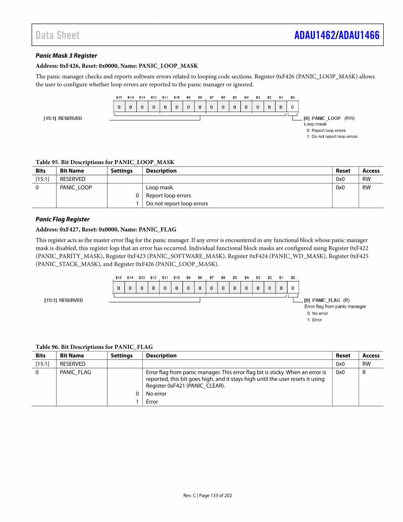
Data Sheet ADAU1462/ADAU1466
Rev. C | Page 133 of 202
Panic Mask 3 Register
Address: 0xF426, Reset: 0x0000, Name: PANIC_LOOP_MASK
The panic manager checks and reports software errors related to looping code sections. Register 0xF426 (PANIC_LOOP_MASK) allows the user to configure whether loop errors are reported to the panic manager or ignored.
Table 95. Bit Descriptions for PANIC_LOOP_MASK Bits Bit Name Settings Description Reset Access [15:1] RESERVED 0x0 RW 0 PANIC_LOOP Loop mask. 0x0 RW 0 Report loop errors 1 Do not report loop errors
Panic Flag Register
Address: 0xF427, Reset: 0x0000, Name: PANIC_FLAG
This register acts as the master error flag for the panic manager. If any error is encountered in any functional block whose panic manager mask is disabled, this register logs that an error has occurred. Individual functional block masks are configured using Register 0xF422 (PANIC_PARITY_MASK), Register 0xF423 (PANIC_SOFTWARE_MASK), Register 0xF424 (PANIC_WD_MASK), Register 0xF425 (PANIC_STACK_MASK), and Register 0xF426 (PANIC_LOOP_MASK).
Table 96. Bit Descriptions for PANIC_FLAG Bits Bit Name Settings Description Reset Access [15:1] RESERVED 0x0 RW 0 PANIC_FLAG Error flag from panic manager. This error flag bit is sticky. When an error is
reported, this bit goes high, and it stays high until the user resets it using Register 0xF421 (PANIC_CLEAR).
0x0 R
0 No error 1 Error
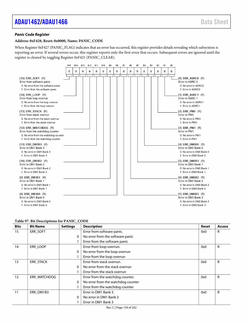
ADAU1462/ADAU1466 Data Sheet
Rev. C | Page 134 of 202
Panic Code Register
Address: 0xF428, Reset: 0x0000, Name: PANIC_CODE
When Register 0xF427 (PANIC_FLAG) indicates that an error has occurred, this register provides details revealing which subsystem is reporting an error. If several errors occur, this register reports only the first error that occurs. Subsequent errors are ignored until the register is cleared by toggling Register 0xF421 (PANIC_CLEAR).
Table 97. Bit Descriptions for PANIC_CODE Bits Bit Name Settings Description Reset Access 15 ERR_SOFT Error from software panic. 0x0 R 0 No error from the software panic 1 Error from the software panic 14 ERR_LOOP Error from loop overrun. 0x0 R 0 No error from the loop overrun 1 Error from the loop overrun 13 ERR_STACK Error from stack overrun. 0x0 R 0 No error from the stack overrun 1 Error from the stack overrun 12 ERR_WATCHDOG Error from the watchdog counter. 0x0 R 0 No error from the watchdog counter 1 Error from the watchdog counter 11 ERR_DM1B3 Error in DM1 Bank 3. 0x0 R 0 No error in DM1 Bank 3 1 Error in DM1 Bank 3
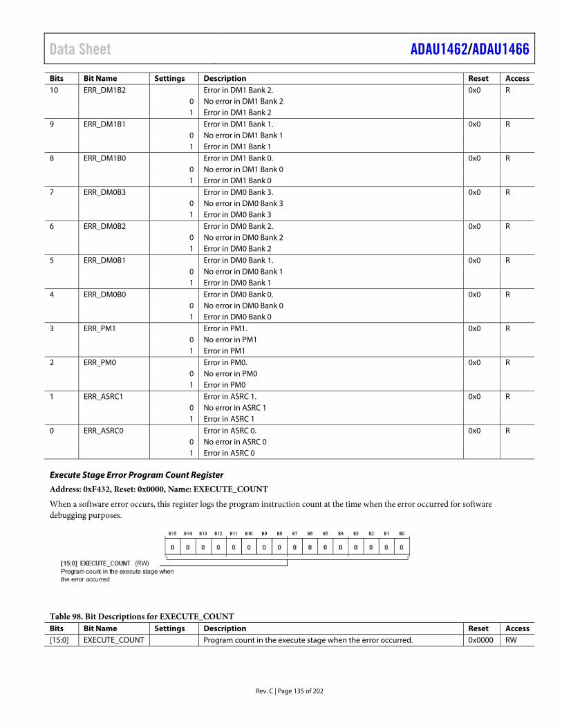
Data Sheet ADAU1462/ADAU1466
Rev. C | Page 135 of 202
Bits Bit Name Settings Description Reset Access 10 ERR_DM1B2 Error in DM1 Bank 2. 0x0 R 0 No error in DM1 Bank 2 1 Error in DM1 Bank 2 9 ERR_DM1B1 Error in DM1 Bank 1. 0x0 R 0 No error in DM1 Bank 1 1 Error in DM1 Bank 1 8 ERR_DM1B0 Error in DM1 Bank 0. 0x0 R 0 No error in DM1 Bank 0 1 Error in DM1 Bank 0 7 ERR_DM0B3 Error in DM0 Bank 3. 0x0 R 0 No error in DM0 Bank 3 1 Error in DM0 Bank 3 6 ERR_DM0B2 Error in DM0 Bank 2. 0x0 R 0 No error in DM0 Bank 2 1 Error in DM0 Bank 2 5 ERR_DM0B1 Error in DM0 Bank 1. 0x0 R 0 No error in DM0 Bank 1 1 Error in DM0 Bank 1 4 ERR_DM0B0 Error in DM0 Bank 0. 0x0 R 0 No error in DM0 Bank 0 1 Error in DM0 Bank 0 3 ERR_PM1 Error in PM1. 0x0 R 0 No error in PM1 1 Error in PM1 2 ERR_PM0 Error in PM0. 0x0 R 0 No error in PM0 1 Error in PM0 1 ERR_ASRC1 Error in ASRC 1. 0x0 R 0 No error in ASRC 1 1 Error in ASRC 1 0 ERR_ASRC0 Error in ASRC 0. 0x0 R 0 No error in ASRC 0 1 Error in ASRC 0
Execute Stage Error Program Count Register
Address: 0xF432, Reset: 0x0000, Name: EXECUTE_COUNT
When a software error occurs, this register logs the program instruction count at the time when the error occurred for software debugging purposes.
Table 98. Bit Descriptions for EXECUTE_COUNT Bits Bit Name Settings Description Reset Access [15:0] EXECUTE_COUNT Program count in the execute stage when the error occurred. 0x0000 RW
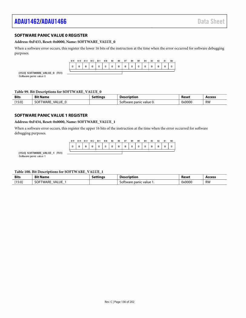
ADAU1462/ADAU1466 Data Sheet
Rev. C | Page 136 of 202
SOFTWARE PANIC VALUE 0 REGISTER Address: 0xF433, Reset: 0x0000, Name: SOFTWARE_VALUE_0
When a software error occurs, this register the lower 16 bits of the instruction at the time when the error occurred for software debugging purposes.
Table 99. Bit Descriptions for SOFTWARE_VALUE_0 Bits Bit Name Settings Description Reset Access [15:0] SOFTWARE_VALUE_0 Software panic value 0. 0x0000 RW
SOFTWARE PANIC VALUE 1 REGISTER Address: 0xF434, Reset: 0x0000, Name: SOFTWARE_VALUE_1
When a software error occurs, this register the upper 16 bits of the instruction at the time when the error occurred for software debugging purposes.
Table 100. Bit Descriptions for SOFTWARE_VALUE_1 Bits Bit Name Settings Description Reset Access [15:0] SOFTWARE_VALUE_1 Software panic value 1. 0x0000 RW
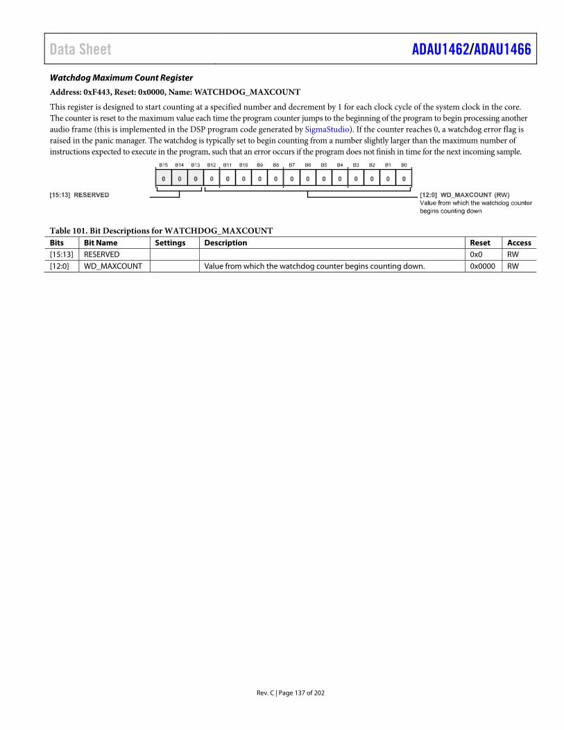
Data Sheet ADAU1462/ADAU1466
Rev. C | Page 137 of 202
Watchdog Maximum Count Register
Address: 0xF443, Reset: 0x0000, Name: WATCHDOG_MAXCOUNT
This register is designed to start counting at a specified number and decrement by 1 for each clock cycle of the system clock in the core. The counter is reset to the maximum value each time the program counter jumps to the beginning of the program to begin processing another audio frame (this is implemented in the DSP program code generated by SigmaStudio). If the counter reaches 0, a watchdog error flag is raised in the panic manager. The watchdog is typically set to begin counting from a number slightly larger than the maximum number of instructions expected to execute in the program, such that an error occurs if the program does not finish in time for the next incoming sample.
Table 101. Bit Descriptions for WATCHDOG_MAXCOUNT Bits Bit Name Settings Description Reset Access [15:13] RESERVED 0x0 RW [12:0] WD_MAXCOUNT Value from which the watchdog counter begins counting down. 0x0000 RW
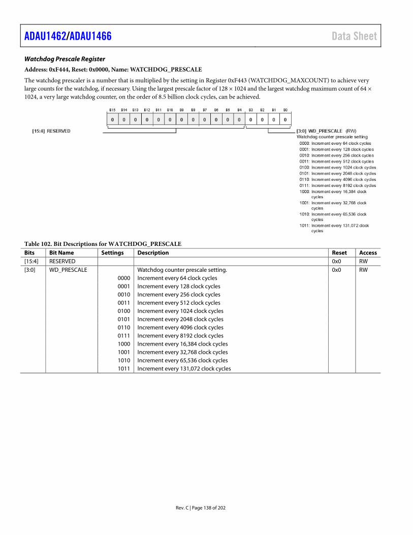
ADAU1462/ADAU1466 Data Sheet
Rev. C | Page 138 of 202
Watchdog Prescale Register
Address: 0xF444, Reset: 0x0000, Name: WATCHDOG_PRESCALE
The watchdog prescaler is a number that is multiplied by the setting in Register 0xF443 (WATCHDOG_MAXCOUNT) to achieve very large counts for the watchdog, if necessary. Using the largest prescale factor of 128 × 1024 and the largest watchdog maximum count of 64 × 1024, a very large watchdog counter, on the order of 8.5 billion clock cycles, can be achieved.
Table 102. Bit Descriptions for WATCHDOG_PRESCALE Bits Bit Name Settings Description Reset Access [15:4] RESERVED 0x0 RW [3:0] WD_PRESCALE Watchdog counter prescale setting. 0x0 RW 0000 Increment every 64 clock cycles 0001 Increment every 128 clock cycles 0010 Increment every 256 clock cycles 0011 Increment every 512 clock cycles 0100 Increment every 1024 clock cycles 0101 Increment every 2048 clock cycles 0110 Increment every 4096 clock cycles 0111 Increment every 8192 clock cycles 1000 Increment every 16,384 clock cycles 1001 Increment every 32,768 clock cycles 1010 Increment every 65,536 clock cycles 1011 Increment every 131,072 clock cycles
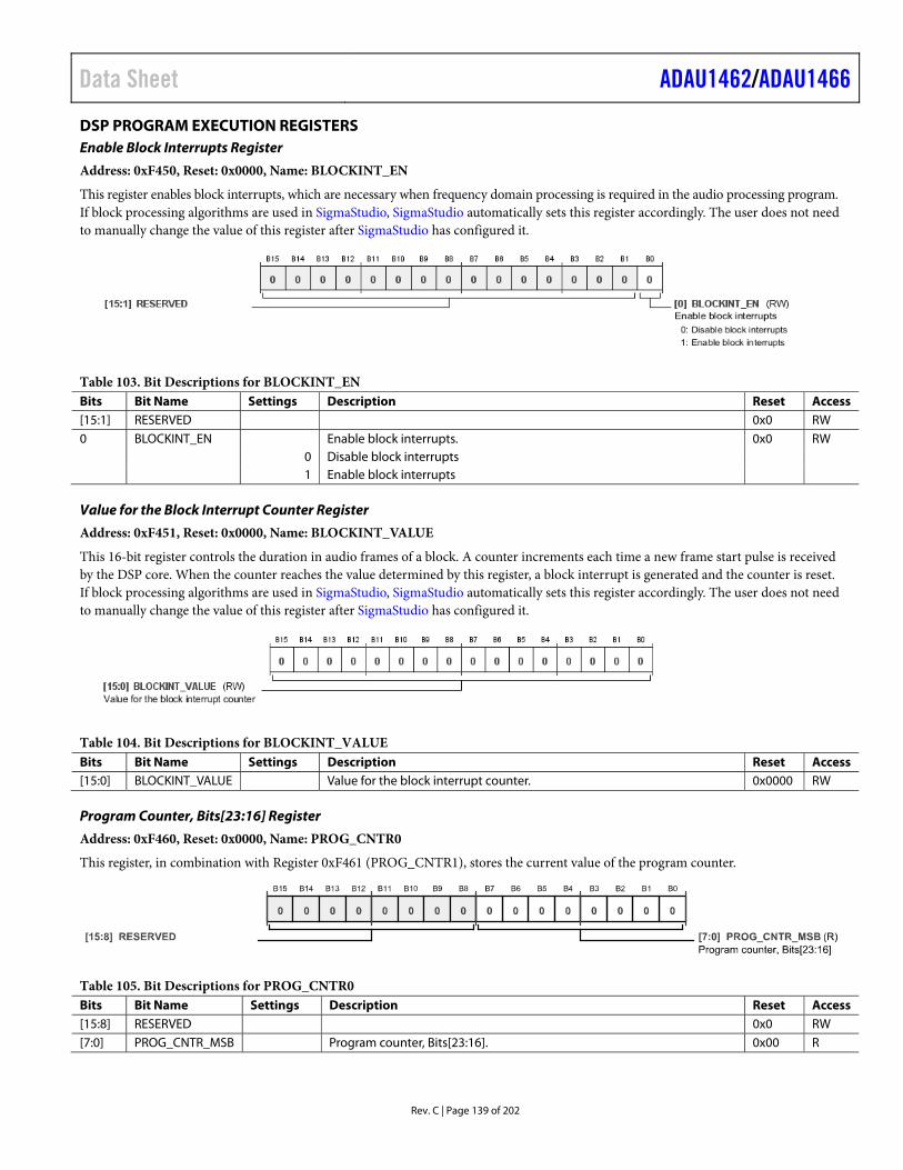
Data Sheet ADAU1462/ADAU1466
Rev. C | Page 139 of 202
DSP PROGRAM EXECUTION REGISTERS Enable Block Interrupts Register
Address: 0xF450, Reset: 0x0000, Name: BLOCKINT_EN
This register enables block interrupts, which are necessary when frequency domain processing is required in the audio processing program. If block processing algorithms are used in SigmaStudio, SigmaStudio automatically sets this register accordingly. The user does not need to manually change the value of this register after SigmaStudio has configured it.
Table 103. Bit Descriptions for BLOCKINT_EN Bits Bit Name Settings Description Reset Access [15:1] RESERVED 0x0 RW 0 BLOCKINT_EN Enable block interrupts. 0x0 RW 0 Disable block interrupts 1 Enable block interrupts
Value for the Block Interrupt Counter Register
Address: 0xF451, Reset: 0x0000, Name: BLOCKINT_VALUE
This 16-bit register controls the duration in audio frames of a block. A counter increments each time a new frame start pulse is received by the DSP core. When the counter reaches the value determined by this register, a block interrupt is generated and the counter is reset. If block processing algorithms are used in SigmaStudio, SigmaStudio automatically sets this register accordingly. The user does not need to manually change the value of this register after SigmaStudio has configured it.
Table 104. Bit Descriptions for BLOCKINT_VALUE Bits Bit Name Settings Description Reset Access [15:0] BLOCKINT_VALUE Value for the block interrupt counter. 0x0000 RW
Program Counter, Bits[23:16] Register
Address: 0xF460, Reset: 0x0000, Name: PROG_CNTR0
This register, in combination with Register 0xF461 (PROG_CNTR1), stores the current value of the program counter.
Table 105. Bit Descriptions for PROG_CNTR0 Bits Bit Name Settings Description Reset Access [15:8] RESERVED 0x0 RW [7:0] PROG_CNTR_MSB Program counter, Bits[23:16]. 0x00 R
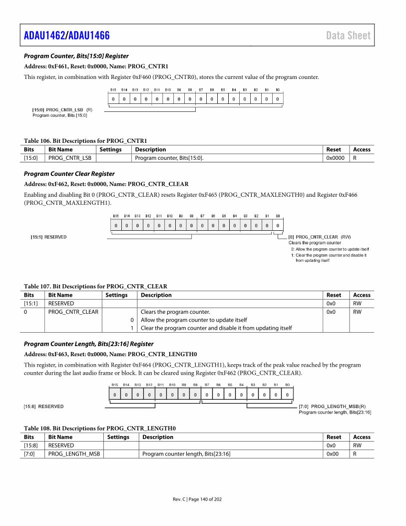
ADAU1462/ADAU1466 Data Sheet
Rev. C | Page 140 of 202
Program Counter, Bits[15:0] Register
Address: 0xF461, Reset: 0x0000, Name: PROG_CNTR1
This register, in combination with Register 0xF460 (PROG_CNTR0), stores the current value of the program counter.
Table 106. Bit Descriptions for PROG_CNTR1 Bits Bit Name Settings Description Reset Access [15:0] PROG_CNTR_LSB Program counter, Bits[15:0]. 0x0000 R
Program Counter Clear Register
Address: 0xF462, Reset: 0x0000, Name: PROG_CNTR_CLEAR
Enabling and disabling Bit 0 (PROG_CNTR_CLEAR) resets Register 0xF465 (PROG_CNTR_MAXLENGTH0) and Register 0xF466 (PROG_CNTR_MAXLENGTH1).
Table 107. Bit Descriptions for PROG_CNTR_CLEAR Bits Bit Name Settings Description Reset Access [15:1] RESERVED 0x0 RW 0 PROG_CNTR_CLEAR Clears the program counter. 0x0 RW 0 Allow the program counter to update itself 1 Clear the program counter and disable it from updating itself
Program Counter Length, Bits[23:16] Register
Address: 0xF463, Reset: 0x0000, Name: PROG_CNTR_LENGTH0
This register, in combination with Register 0xF464 (PROG_CNTR_LENGTH1), keeps track of the peak value reached by the program counter during the last audio frame or block. It can be cleared using Register 0xF462 (PROG_CNTR_CLEAR).
Table 108. Bit Descriptions for PROG_CNTR_LENGTH0 Bits Bit Name Settings Description Reset Access [15:8] RESERVED 0x0 RW [7:0] PROG_LENGTH_MSB Program counter length, Bits[23:16] 0x00 R
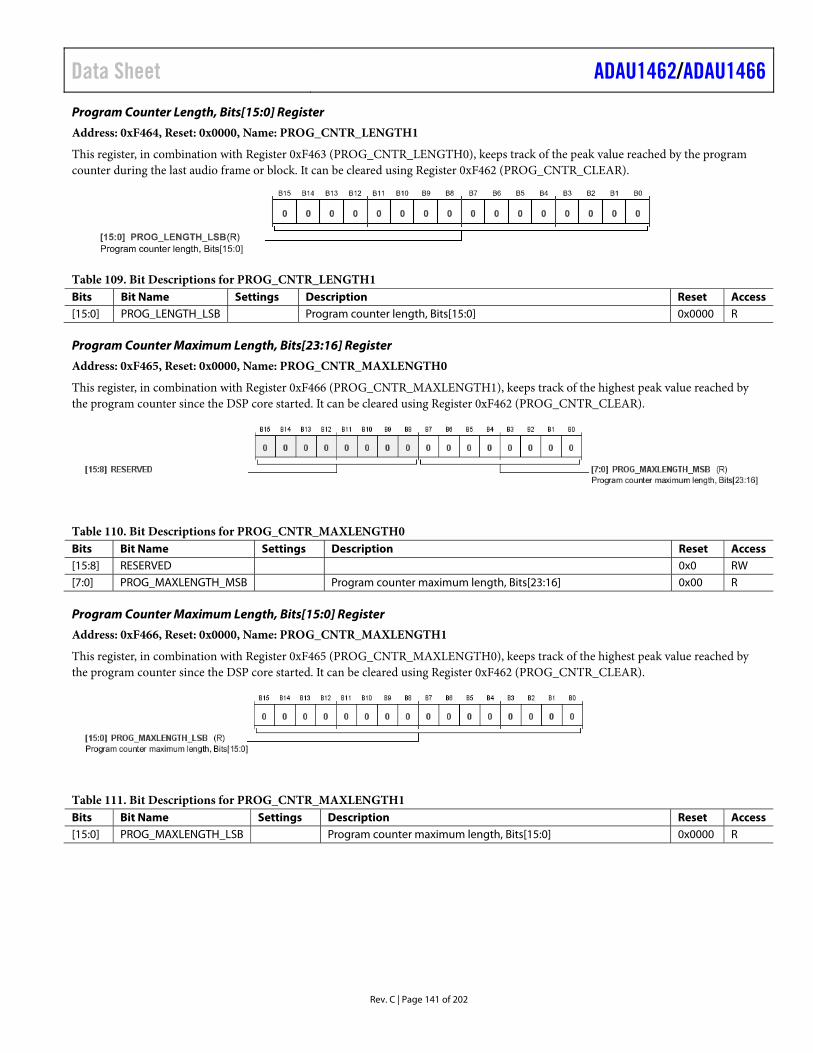
Data Sheet ADAU1462/ADAU1466
Rev. C | Page 141 of 202
Program Counter Length, Bits[15:0] Register
Address: 0xF464, Reset: 0x0000, Name: PROG_CNTR_LENGTH1
This register, in combination with Register 0xF463 (PROG_CNTR_LENGTH0), keeps track of the peak value reached by the program counter during the last audio frame or block. It can be cleared using Register 0xF462 (PROG_CNTR_CLEAR).
Table 109. Bit Descriptions for PROG_CNTR_LENGTH1 Bits Bit Name Settings Description Reset Access [15:0] PROG_LENGTH_LSB Program counter length, Bits[15:0] 0x0000 R
Program Counter Maximum Length, Bits[23:16] Register
Address: 0xF465, Reset: 0x0000, Name: PROG_CNTR_MAXLENGTH0
This register, in combination with Register 0xF466 (PROG_CNTR_MAXLENGTH1), keeps track of the highest peak value reached by the program counter since the DSP core started. It can be cleared using Register 0xF462 (PROG_CNTR_CLEAR).
Table 110. Bit Descriptions for PROG_CNTR_MAXLENGTH0 Bits Bit Name Settings Description Reset Access [15:8] RESERVED 0x0 RW [7:0] PROG_MAXLENGTH_MSB Program counter maximum length, Bits[23:16] 0x00 R
Program Counter Maximum Length, Bits[15:0] Register
Address: 0xF466, Reset: 0x0000, Name: PROG_CNTR_MAXLENGTH1
This register, in combination with Register 0xF465 (PROG_CNTR_MAXLENGTH0), keeps track of the highest peak value reached by the program counter since the DSP core started. It can be cleared using Register 0xF462 (PROG_CNTR_CLEAR).
Table 111. Bit Descriptions for PROG_CNTR_MAXLENGTH1 Bits Bit Name Settings Description Reset Access [15:0] PROG_MAXLENGTH_LSB Program counter maximum length, Bits[15:0] 0x0000 R
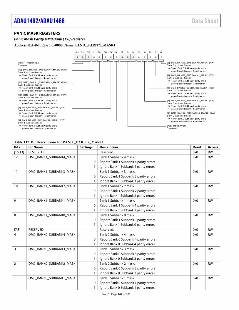
ADAU1462/ADAU1466 Data Sheet
Rev. C | Page 142 of 202
PANIC MASK REGISTERS Panic Mask Parity DM0 Bank [1:0] Register
Address: 0xF467, Reset: 0x0000, Name: PANIC_PARITY_MASK1
Table 112. Bit Descriptions for PANIC_PARITY_MASK1 Bits Bit Name Settings Description Reset Access [15:13] RESERVED Reserved. 0x0 RW 12 DM0_BANK1_SUBBANK4_MASK Bank 1 Subbank 4 mask. 0x0 RW 0 Report Bank 1 Subbank 4 parity errors 1 Ignore Bank 1 Subbank 4 parity errors 11 DM0_BANK1_SUBBANK3_MASK Bank 1 Subbank 3 mask. 0x0 RW 0 Report Bank 1 Subbank 3 parity errors 1 Ignore Bank 1 Subbank 3 parity errors 10 DM0_BANK1_SUBBANK2_MASK Bank 1 Subbank 2 mask. 0x0 RW 0 Report Bank 1 Subbank 2 parity errors 1 Ignore Bank 1 Subbank 2 parity errors 9 DM0_BANK1_SUBBANK1_MASK Bank 1 Subbank 1 mask. 0x0 RW 0 Report Bank 1 Subbank 1 parity errors 1 Ignore Bank 1 Subbank 1 parity errors 8 DM0_BANK1_SUBBANK0_MASK Bank 1 Subbank 0 mask. 0x0 RW 0 Report Bank 1 Subbank 0 parity errors 1 Ignore Bank 1 Subbank 0 parity errors [7:5] RESERVED Reserved. 0x0 RW 4 DM0_BANK0_SUBBANK4_MASK Bank 0 Subbank 4 mask. 0x0 RW 0 Report Bank 0 Subbank 4 parity errors 1 Ignore Bank 0 Subbank 4 parity errors 3 DM0_BANK0_SUBBANK3_MASK Bank 0 Subbank 3 mask. 0x0 RW 0 Report Bank 0 Subbank 3 parity errors 1 Ignore Bank 0 Subbank 3 parity errors 2 DM0_BANK0_SUBBANK2_MASK Bank 0 Subbank 2 mask. 0x0 RW 0 Report Bank 0 Subbank 2 parity errors 1 Ignore Bank 0 Subbank 2 parity errors 1 DM0_BANK0_SUBBANK1_MASK Bank 0 Subbank 1 mask. 0x0 RW 0 Report Bank 0 Subbank 1 parity errors 1 Ignore Bank 0 Subbank 1 parity errors
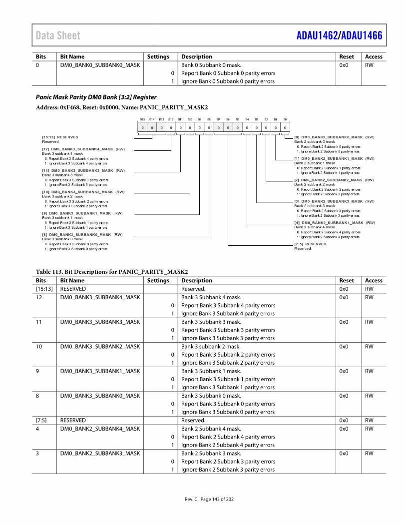
Data Sheet ADAU1462/ADAU1466
Rev. C | Page 143 of 202
Bits Bit Name Settings Description Reset Access 0 DM0_BANK0_SUBBANK0_MASK Bank 0 Subbank 0 mask. 0x0 RW 0 Report Bank 0 Subbank 0 parity errors 1 Ignore Bank 0 Subbank 0 parity errors
Panic Mask Parity DM0 Bank [3:2] Register
Address: 0xF468, Reset: 0x0000, Name: PANIC_PARITY_MASK2
Table 113. Bit Descriptions for PANIC_PARITY_MASK2 Bits Bit Name Settings Description Reset Access [15:13] RESERVED Reserved. 0x0 RW 12 DM0_BANK3_SUBBANK4_MASK Bank 3 Subbank 4 mask. 0x0 RW 0 Report Bank 3 Subbank 4 parity errors 1 Ignore Bank 3 Subbank 4 parity errors 11 DM0_BANK3_SUBBANK3_MASK Bank 3 Subbank 3 mask. 0x0 RW 0 Report Bank 3 Subbank 3 parity errors 1 Ignore Bank 3 Subbank 3 parity errors 10 DM0_BANK3_SUBBANK2_MASK Bank 3 subbank 2 mask. 0x0 RW 0 Report Bank 3 Subbank 2 parity errors 1 Ignore Bank 3 Subbank 2 parity errors 9 DM0_BANK3_SUBBANK1_MASK Bank 3 Subbank 1 mask. 0x0 RW 0 Report Bank 3 Subbank 1 parity errors 1 Ignore Bank 3 Subbank 1 parity errors 8 DM0_BANK3_SUBBANK0_MASK Bank 3 Subbank 0 mask. 0x0 RW 0 Report Bank 3 Subbank 0 parity errors 1 Ignore Bank 3 Subbank 0 parity errors [7:5] RESERVED Reserved. 0x0 RW 4 DM0_BANK2_SUBBANK4_MASK Bank 2 Subbank 4 mask. 0x0 RW 0 Report Bank 2 Subbank 4 parity errors 1 Ignore Bank 2 Subbank 4 parity errors 3 DM0_BANK2_SUBBANK3_MASK Bank 2 Subbank 3 mask. 0x0 RW 0 Report Bank 2 Subbank 3 parity errors 1 Ignore Bank 2 Subbank 3 parity errors
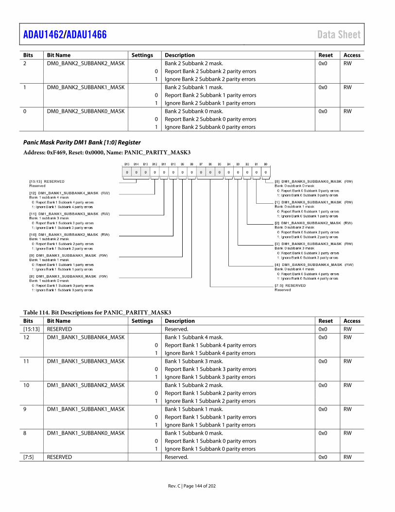
ADAU1462/ADAU1466 Data Sheet
Rev. C | Page 144 of 202
Bits Bit Name Settings Description Reset Access 2 DM0_BANK2_SUBBANK2_MASK Bank 2 Subbank 2 mask. 0x0 RW 0 Report Bank 2 Subbank 2 parity errors 1 Ignore Bank 2 Subbank 2 parity errors 1 DM0_BANK2_SUBBANK1_MASK Bank 2 Subbank 1 mask. 0x0 RW 0 Report Bank 2 Subbank 1 parity errors 1 Ignore Bank 2 Subbank 1 parity errors 0 DM0_BANK2_SUBBANK0_MASK Bank 2 Subbank 0 mask. 0x0 RW 0 Report Bank 2 Subbank 0 parity errors 1 Ignore Bank 2 Subbank 0 parity errors
Panic Mask Parity DM1 Bank [1:0] Register
Address: 0xF469, Reset: 0x0000, Name: PANIC_PARITY_MASK3
Table 114. Bit Descriptions for PANIC_PARITY_MASK3 Bits Bit Name Settings Description Reset Access [15:13] RESERVED Reserved. 0x0 RW 12 DM1_BANK1_SUBBANK4_MASK Bank 1 Subbank 4 mask. 0x0 RW 0 Report Bank 1 Subbank 4 parity errors 1 Ignore Bank 1 Subbank 4 parity errors 11 DM1_BANK1_SUBBANK3_MASK Bank 1 Subbank 3 mask. 0x0 RW 0 Report Bank 1 Subbank 3 parity errors 1 Ignore Bank 1 Subbank 3 parity errors 10 DM1_BANK1_SUBBANK2_MASK Bank 1 Subbank 2 mask. 0x0 RW 0 Report Bank 1 Subbank 2 parity errors 1 Ignore Bank 1 Subbank 2 parity errors 9 DM1_BANK1_SUBBANK1_MASK Bank 1 Subbank 1 mask. 0x0 RW 0 Report Bank 1 Subbank 1 parity errors 1 Ignore Bank 1 Subbank 1 parity errors 8 DM1_BANK1_SUBBANK0_MASK Bank 1 Subbank 0 mask. 0x0 RW 0 Report Bank 1 Subbank 0 parity errors 1 Ignore Bank 1 Subbank 0 parity errors [7:5] RESERVED Reserved. 0x0 RW
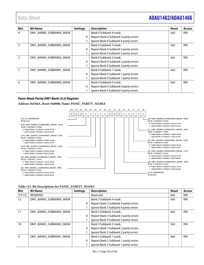
Data Sheet ADAU1462/ADAU1466
Rev. C | Page 145 of 202
Bits Bit Name Settings Description Reset Access 4 DM1_BANK0_SUBBANK4_MASK Bank 0 Subbank 4 mask. 0x0 RW 0 Report Bank 0 Subbank 4 parity errors 1 Ignore Bank 0 Subbank 4 parity errors 3 DM1_BANK0_SUBBANK3_MASK Bank 0 Subbank 3 mask. 0x0 RW 0 Report Bank 0 Subbank 3 parity errors 1 Ignore Bank 0 Subbank 3 parity errors 2 DM1_BANK0_SUBBANK2_MASK Bank 0 Subbank 2 mask. 0x0 RW 0 Report Bank 0 Subbank 2 parity errors 1 Ignore Bank 0 Subbank 2 parity errors 1 DM1_BANK0_SUBBANK1_MASK Bank 0 Subbank 1 mask. 0x0 RW 0 Report Bank 0 Subbank 1 parity errors 1 Ignore Bank 0 Subbank 1 parity errors 0 DM1_BANK0_SUBBANK0_MASK Bank 0 Subbank 0 mask. 0x0 RW 0 Report Bank 0 Subbank 0 parity errors 1 Ignore Bank 0 Subbank 0 parity errors
Panic Mask Parity DM1 Bank [3:2] Register
Address: 0xF46A, Reset: 0x0000, Name: PANIC_PARITY_MASK4
Table 115. Bit Descriptions for PANIC_PARITY_MASK4 Bits Bit Name Settings Description Reset Access [15:13] RESERVED Reserved. 0x0 RW 12 DM1_BANK3_SUBBANK4_MASK Bank 3 Subbank 4 mask. 0x0 RW 0 Report Bank 3 Subbank 4 parity errors 1 Ignore Bank 3 Subbank 4 parity errors 11 DM1_BANK3_SUBBANK3_MASK Bank 3 Subbank 3 mask. 0x0 RW 0 Report Bank 3 Subbank 3 parity errors 1 Ignore Bank 3 Subbank 3 parity errors 10 DM1_BANK3_SUBBANK2_MASK Bank 3 Subbank 2 mask. 0x0 RW 0 Report Bank 3 Subbank 2 parity errors 1 Ignore Bank 3 Subbank 2 parity errors 9 DM1_BANK3_SUBBANK1_MASK Bank 3 Subbank 1 mask. 0x0 RW 0 Report Bank 3 Subbank 1 parity errors 1 Ignore Bank 3 Subbank 1 parity errors
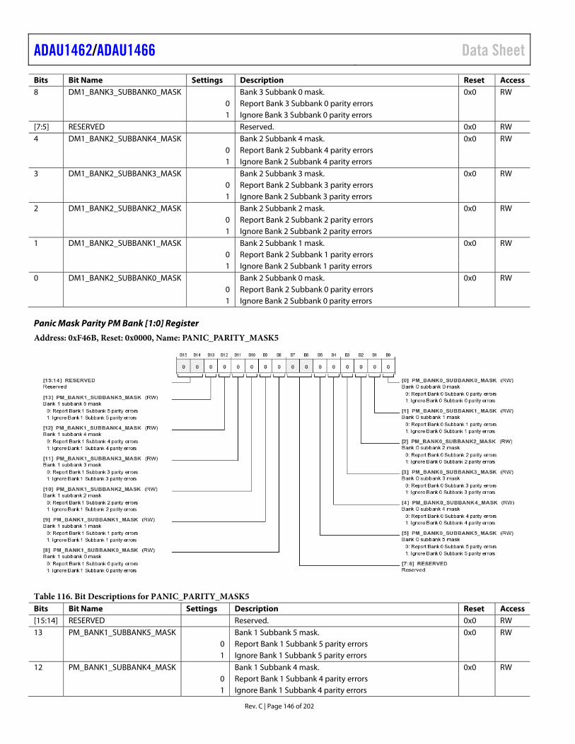
ADAU1462/ADAU1466 Data Sheet
Rev. C | Page 146 of 202
Bits Bit Name Settings Description Reset Access 8 DM1_BANK3_SUBBANK0_MASK Bank 3 Subbank 0 mask. 0x0 RW 0 Report Bank 3 Subbank 0 parity errors 1 Ignore Bank 3 Subbank 0 parity errors [7:5] RESERVED Reserved. 0x0 RW 4 DM1_BANK2_SUBBANK4_MASK Bank 2 Subbank 4 mask. 0x0 RW 0 Report Bank 2 Subbank 4 parity errors 1 Ignore Bank 2 Subbank 4 parity errors 3 DM1_BANK2_SUBBANK3_MASK Bank 2 Subbank 3 mask. 0x0 RW 0 Report Bank 2 Subbank 3 parity errors 1 Ignore Bank 2 Subbank 3 parity errors 2 DM1_BANK2_SUBBANK2_MASK Bank 2 Subbank 2 mask. 0x0 RW 0 Report Bank 2 Subbank 2 parity errors 1 Ignore Bank 2 Subbank 2 parity errors 1 DM1_BANK2_SUBBANK1_MASK Bank 2 Subbank 1 mask. 0x0 RW 0 Report Bank 2 Subbank 1 parity errors 1 Ignore Bank 2 Subbank 1 parity errors 0 DM1_BANK2_SUBBANK0_MASK Bank 2 Subbank 0 mask. 0x0 RW 0 Report Bank 2 Subbank 0 parity errors 1 Ignore Bank 2 Subbank 0 parity errors
Panic Mask Parity PM Bank [1:0] Register
Address: 0xF46B, Reset: 0x0000, Name: PANIC_PARITY_MASK5
Table 116. Bit Descriptions for PANIC_PARITY_MASK5 Bits Bit Name Settings Description Reset Access [15:14] RESERVED Reserved. 0x0 RW 13 PM_BANK1_SUBBANK5_MASK Bank 1 Subbank 5 mask. 0x0 RW 0 Report Bank 1 Subbank 5 parity errors 1 Ignore Bank 1 Subbank 5 parity errors 12 PM_BANK1_SUBBANK4_MASK Bank 1 Subbank 4 mask. 0x0 RW 0 Report Bank 1 Subbank 4 parity errors 1 Ignore Bank 1 Subbank 4 parity errors
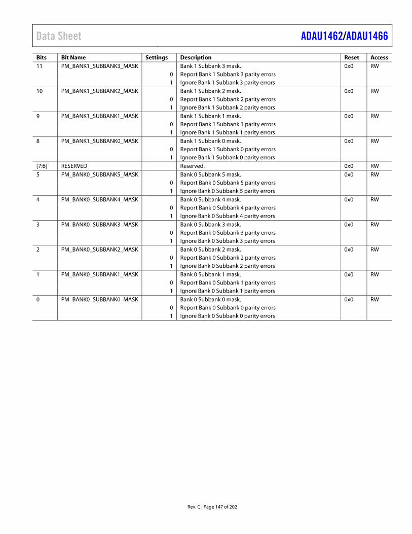
Data Sheet ADAU1462/ADAU1466
Rev. C | Page 147 of 202
Bits Bit Name Settings Description Reset Access 11 PM_BANK1_SUBBANK3_MASK Bank 1 Subbank 3 mask. 0x0 RW 0 Report Bank 1 Subbank 3 parity errors 1 Ignore Bank 1 Subbank 3 parity errors 10 PM_BANK1_SUBBANK2_MASK Bank 1 Subbank 2 mask. 0x0 RW 0 Report Bank 1 Subbank 2 parity errors 1 Ignore Bank 1 Subbank 2 parity errors 9 PM_BANK1_SUBBANK1_MASK Bank 1 Subbank 1 mask. 0x0 RW 0 Report Bank 1 Subbank 1 parity errors 1 Ignore Bank 1 Subbank 1 parity errors 8 PM_BANK1_SUBBANK0_MASK Bank 1 Subbank 0 mask. 0x0 RW 0 Report Bank 1 Subbank 0 parity errors 1 Ignore Bank 1 Subbank 0 parity errors [7:6] RESERVED Reserved. 0x0 RW 5 PM_BANK0_SUBBANK5_MASK Bank 0 Subbank 5 mask. 0x0 RW 0 Report Bank 0 Subbank 5 parity errors 1 Ignore Bank 0 Subbank 5 parity errors 4 PM_BANK0_SUBBANK4_MASK Bank 0 Subbank 4 mask. 0x0 RW 0 Report Bank 0 Subbank 4 parity errors 1 Ignore Bank 0 Subbank 4 parity errors 3 PM_BANK0_SUBBANK3_MASK Bank 0 Subbank 3 mask. 0x0 RW 0 Report Bank 0 Subbank 3 parity errors 1 Ignore Bank 0 Subbank 3 parity errors 2 PM_BANK0_SUBBANK2_MASK Bank 0 Subbank 2 mask. 0x0 RW 0 Report Bank 0 Subbank 2 parity errors 1 Ignore Bank 0 Subbank 2 parity errors 1 PM_BANK0_SUBBANK1_MASK Bank 0 Subbank 1 mask. 0x0 RW 0 Report Bank 0 Subbank 1 parity errors 1 Ignore Bank 0 Subbank 1 parity errors 0 PM_BANK0_SUBBANK0_MASK Bank 0 Subbank 0 mask. 0x0 RW 0 Report Bank 0 Subbank 0 parity errors 1 Ignore Bank 0 Subbank 0 parity errors
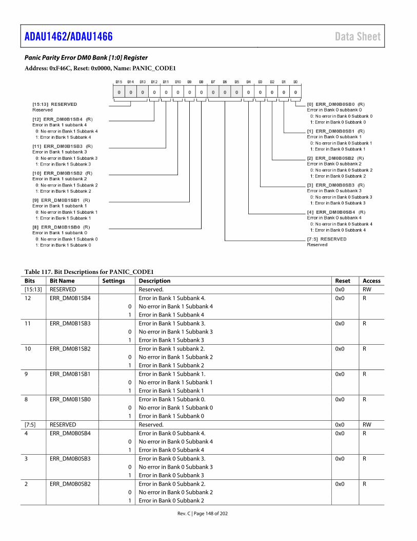
ADAU1462/ADAU1466 Data Sheet
Rev. C | Page 148 of 202
Panic Parity Error DM0 Bank [1:0] Register
Address: 0xF46C, Reset: 0x0000, Name: PANIC_CODE1
Table 117. Bit Descriptions for PANIC_CODE1 Bits Bit Name Settings Description Reset Access [15:13] RESERVED Reserved. 0x0 RW 12 ERR_DM0B1SB4 Error in Bank 1 Subbank 4. 0x0 R 0 No error in Bank 1 Subbank 4 1 Error in Bank 1 Subbank 4 11 ERR_DM0B1SB3 Error in Bank 1 Subbank 3. 0x0 R 0 No error in Bank 1 Subbank 3 1 Error in Bank 1 Subbank 3 10 ERR_DM0B1SB2 Error in Bank 1 subbank 2. 0x0 R 0 No error in Bank 1 Subbank 2 1 Error in Bank 1 Subbank 2 9 ERR_DM0B1SB1 Error in Bank 1 Subbank 1. 0x0 R 0 No error in Bank 1 Subbank 1 1 Error in Bank 1 Subbank 1 8 ERR_DM0B1SB0 Error in Bank 1 Subbank 0. 0x0 R 0 No error in Bank 1 Subbank 0 1 Error in Bank 1 Subbank 0 [7:5] RESERVED Reserved. 0x0 RW 4 ERR_DM0B0SB4 Error in Bank 0 Subbank 4. 0x0 R 0 No error in Bank 0 Subbank 4 1 Error in Bank 0 Subbank 4 3 ERR_DM0B0SB3 Error in Bank 0 Subbank 3. 0x0 R 0 No error in Bank 0 Subbank 3 1 Error in Bank 0 Subbank 3 2 ERR_DM0B0SB2 Error in Bank 0 Subbank 2. 0x0 R 0 No error in Bank 0 Subbank 2 1 Error in Bank 0 Subbank 2
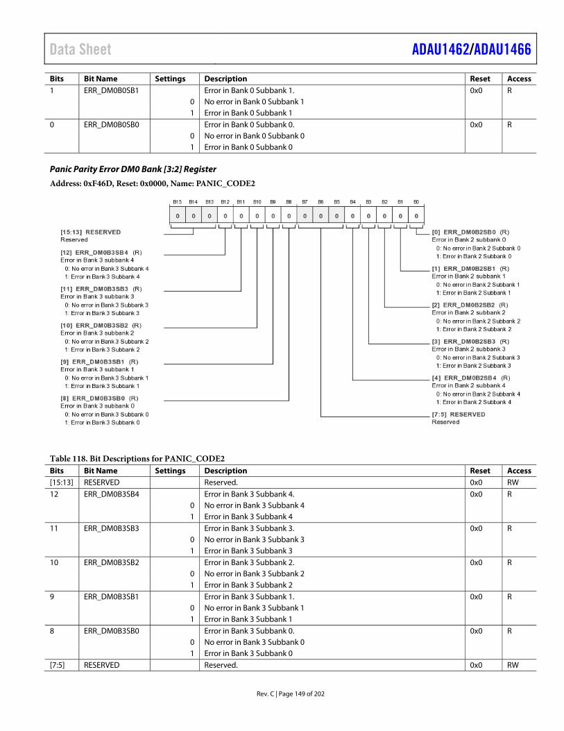
Data Sheet ADAU1462/ADAU1466
Rev. C | Page 149 of 202
Bits Bit Name Settings Description Reset Access 1 ERR_DM0B0SB1 Error in Bank 0 Subbank 1. 0x0 R 0 No error in Bank 0 Subbank 1 1 Error in Bank 0 Subbank 1 0 ERR_DM0B0SB0 Error in Bank 0 Subbank 0. 0x0 R 0 No error in Bank 0 Subbank 0 1 Error in Bank 0 Subbank 0
Panic Parity Error DM0 Bank [3:2] Register
Address: 0xF46D, Reset: 0x0000, Name: PANIC_CODE2
Table 118. Bit Descriptions for PANIC_CODE2 Bits Bit Name Settings Description Reset Access [15:13] RESERVED Reserved. 0x0 RW 12 ERR_DM0B3SB4 Error in Bank 3 Subbank 4. 0x0 R 0 No error in Bank 3 Subbank 4 1 Error in Bank 3 Subbank 4 11 ERR_DM0B3SB3 Error in Bank 3 Subbank 3. 0x0 R 0 No error in Bank 3 Subbank 3 1 Error in Bank 3 Subbank 3 10 ERR_DM0B3SB2 Error in Bank 3 Subbank 2. 0x0 R 0 No error in Bank 3 Subbank 2 1 Error in Bank 3 Subbank 2 9 ERR_DM0B3SB1 Error in Bank 3 Subbank 1. 0x0 R 0 No error in Bank 3 Subbank 1 1 Error in Bank 3 Subbank 1 8 ERR_DM0B3SB0 Error in Bank 3 Subbank 0. 0x0 R 0 No error in Bank 3 Subbank 0 1 Error in Bank 3 Subbank 0 [7:5] RESERVED Reserved. 0x0 RW
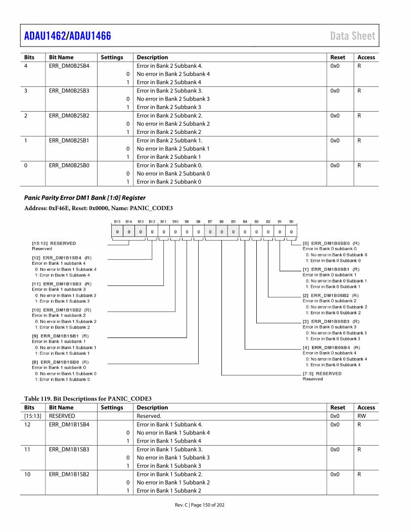
ADAU1462/ADAU1466 Data Sheet
Rev. C | Page 150 of 202
Bits Bit Name Settings Description Reset Access 4 ERR_DM0B2SB4 Error in Bank 2 Subbank 4. 0x0 R 0 No error in Bank 2 Subbank 4 1 Error in Bank 2 Subbank 4 3 ERR_DM0B2SB3 Error in Bank 2 Subbank 3. 0x0 R 0 No error in Bank 2 Subbank 3 1 Error in Bank 2 Subbank 3 2 ERR_DM0B2SB2 Error in Bank 2 Subbank 2. 0x0 R 0 No error in Bank 2 Subbank 2 1 Error in Bank 2 Subbank 2 1 ERR_DM0B2SB1 Error in Bank 2 Subbank 1. 0x0 R 0 No error in Bank 2 Subbank 1 1 Error in Bank 2 Subbank 1 0 ERR_DM0B2SB0 Error in Bank 2 Subbank 0. 0x0 R 0 No error in Bank 2 Subbank 0 1 Error in Bank 2 Subbank 0
Panic Parity Error DM1 Bank [1:0] Register
Address: 0xF46E, Reset: 0x0000, Name: PANIC_CODE3
Table 119. Bit Descriptions for PANIC_CODE3 Bits Bit Name Settings Description Reset Access [15:13] RESERVED Reserved. 0x0 RW 12 ERR_DM1B1SB4 Error in Bank 1 Subbank 4. 0x0 R 0 No error in Bank 1 Subbank 4 1 Error in Bank 1 Subbank 4 11 ERR_DM1B1SB3 Error in Bank 1 Subbank 3. 0x0 R 0 No error in Bank 1 Subbank 3 1 Error in Bank 1 Subbank 3 10 ERR_DM1B1SB2 Error in Bank 1 Subbank 2. 0x0 R 0 No error in Bank 1 Subbank 2 1 Error in Bank 1 Subbank 2
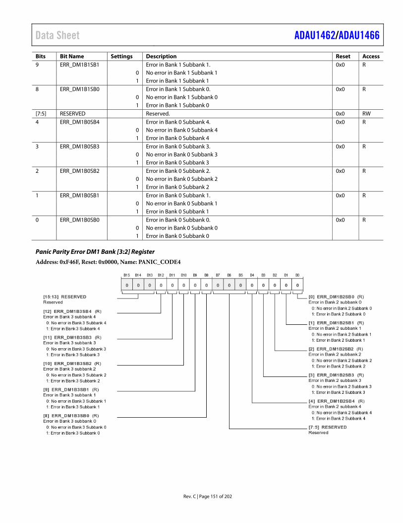
Data Sheet ADAU1462/ADAU1466
Rev. C | Page 151 of 202
Bits Bit Name Settings Description Reset Access 9 ERR_DM1B1SB1 Error in Bank 1 Subbank 1. 0x0 R 0 No error in Bank 1 Subbank 1 1 Error in Bank 1 Subbank 1 8 ERR_DM1B1SB0 Error in Bank 1 Subbank 0. 0x0 R 0 No error in Bank 1 Subbank 0 1 Error in Bank 1 Subbank 0 [7:5] RESERVED Reserved. 0x0 RW 4 ERR_DM1B0SB4 Error in Bank 0 Subbank 4. 0x0 R 0 No error in Bank 0 Subbank 4 1 Error in Bank 0 Subbank 4 3 ERR_DM1B0SB3 Error in Bank 0 Subbank 3. 0x0 R 0 No error in Bank 0 Subbank 3 1 Error in Bank 0 Subbank 3 2 ERR_DM1B0SB2 Error in Bank 0 Subbank 2. 0x0 R 0 No error in Bank 0 Subbank 2 1 Error in Bank 0 Subbank 2 1 ERR_DM1B0SB1 Error in Bank 0 Subbank 1. 0x0 R 0 No error in Bank 0 Subbank 1 1 Error in Bank 0 Subbank 1 0 ERR_DM1B0SB0 Error in Bank 0 Subbank 0. 0x0 R 0 No error in Bank 0 Subbank 0 1 Error in Bank 0 Subbank 0
Panic Parity Error DM1 Bank [3:2] Register
Address: 0xF46F, Reset: 0x0000, Name: PANIC_CODE4
ADAU1462/ADAU1466 Data Sheet
Rev. C | Page 152 of 202
Table 120. Bit Descriptions for PANIC_CODE4 Bits Bit Name Settings Description Reset Access [15:13] RESERVED Reserved. 0x0 RW 12 ERR_DM1B3SB4 Error in Bank 3 Subbank 4. 0x0 R 0 No error in Bank 3 Subbank 4 1 Error in Bank 3 Subbank 4 11 ERR_DM1B3SB3 Error in Bank 3 Subbank 3. 0x0 R 0 No error in Bank 3 Subbank 3 1 Error in Bank 3 Subbank 3 10 ERR_DM1B3SB2 Error in Bank 3 Subbank 2. 0x0 R 0 No error in Bank 3 Subbank 2 1 Error in Bank 3 Subbank 2 9 ERR_DM1B3SB1 Error in Bank 3 Subbank 1. 0x0 R 0 No error in Bank 3 Subbank 1 1 Error in Bank 3 Subbank 1 8 ERR_DM1B3SB0 Error in Bank 3 Subbank 0. 0x0 R 0 No error in Bank 3 Subbank 0 1 Error in Bank 3 Subbank 0 [7:5] RESERVED Reserved. 0x0 RW 4 ERR_DM1B2SB4 Error in Bank 2 Subbank 4. 0x0 R 0 No error in Bank 2 Subbank 4 1 Error in Bank 2 Subbank 4 3 ERR_DM1B2SB3 Error in Bank 2 Subbank 3. 0x0 R 0 No error in Bank 2 Subbank 3 1 Error in Bank 2 Subbank 3 2 ERR_DM1B2SB2 Error in Bank 2 Subbank 2. 0x0 R 0 No error in Bank 2 Subbank 2 1 Error in Bank 2 Subbank 2 1 ERR_DM1B2SB1 Error in Bank 2 Subbank 1. 0x0 R 0 No error in Bank 2 Subbank 1 1 Error in Bank 2 Subbank 1 0 ERR_DM1B2SB0 Error in Bank 2 Subbank 0. 0x0 R 0 No error in Bank 2 Subbank 0 1 Error in Bank 2 Subbank 0
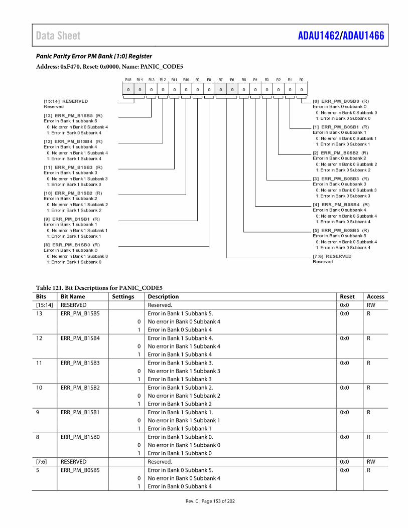
Data Sheet ADAU1462/ADAU1466
Rev. C | Page 153 of 202
Panic Parity Error PM Bank [1:0] Register
Address: 0xF470, Reset: 0x0000, Name: PANIC_CODE5
Table 121. Bit Descriptions for PANIC_CODE5 Bits Bit Name Settings Description Reset Access [15:14] RESERVED Reserved. 0x0 RW 13 ERR_PM_B1SB5 Error in Bank 1 Subbank 5. 0x0 R 0 No error in Bank 0 Subbank 4 1 Error in Bank 0 Subbank 4 12 ERR_PM_B1SB4 Error in Bank 1 Subbank 4. 0x0 R 0 No error in Bank 1 Subbank 4 1 Error in Bank 1 Subbank 4 11 ERR_PM_B1SB3 Error in Bank 1 Subbank 3. 0x0 R 0 No error in Bank 1 Subbank 3 1 Error in Bank 1 Subbank 3 10 ERR_PM_B1SB2 Error in Bank 1 Subbank 2. 0x0 R 0 No error in Bank 1 Subbank 2 1 Error in Bank 1 Subbank 2 9 ERR_PM_B1SB1 Error in Bank 1 Subbank 1. 0x0 R 0 No error in Bank 1 Subbank 1 1 Error in Bank 1 Subbank 1 8 ERR_PM_B1SB0 Error in Bank 1 Subbank 0. 0x0 R 0 No error in Bank 1 Subbank 0 1 Error in Bank 1 Subbank 0 [7:6] RESERVED Reserved. 0x0 RW 5 ERR_PM_B0SB5 Error in Bank 0 Subbank 5. 0x0 R 0 No error in Bank 0 Subbank 4 1 Error in Bank 0 Subbank 4
ADAU1462/ADAU1466 Data Sheet
Rev. C | Page 154 of 202
Bits Bit Name Settings Description Reset Access 4 ERR_PM_B0SB4 Error in Bank 0 Subbank 4. 0x0 R 0 No error in Bank 0 Subbank 4 1 Error in Bank 0 Subbank 4 3 ERR_PM_B0SB3 Error in Bank 0 Subbank 3. 0x0 R 0 No error in Bank 0 Subbank 3 1 Error in Bank 0 Subbank 3 2 ERR_PM_B0SB2 Error in Bank 0 Subbank 2. 0x0 R 0 No error in Bank 0 Subbank 2 1 Error in Bank 0 Subbank 2 1 ERR_PM_B0SB1 Error in Bank 0 Subbank 1. 0x0 R 0 No error in Bank 0 Subbank 1 1 Error in Bank 0 Subbank 1 0 ERR_PM_B0SB0 Error in Bank 0 Subbank 0. 0x0 R 0 No error in Bank 0 Subbank 0 1 Error in Bank 0 Subbank 0
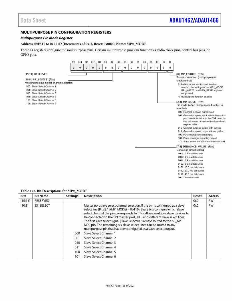
Data Sheet ADAU1462/ADAU1466
Rev. C | Page 155 of 202
MULTIPURPOSE PIN CONFIGURATION REGISTERS Multipurpose Pin Mode Register
Address: 0xF510 to 0xF51D (Increments of 0x1), Reset: 0x0000, Name: MPx_MODE
These 14 registers configure the multipurpose pins. Certain multipurpose pins can function as audio clock pins, control bus pins, or GPIO pins.
Table 122. Bit Descriptions for MPx_MODE Bits Bit Name Settings Description Reset Access [15:11] RESERVED 0x0 RW [10:8] SS_SELECT Master port slave select channel selection. If the pin is configured as a slave
select line (Bits[3:1] (MP_MODE) = 0b110), these bits configure which slave select channel the pin corresponds to. This allows multiple slave devices to be connected to the SPI master port, all using different slave select lines. The first slave select signal (Slave Select 0) is always routed to the SS_M/ MP0 pin. The remaining six slave select lines can be routed to any multipurpose pin that has been configured as a slave select output.
0x0 RW
000 Slave Select Channel 1 001 Slave Select Channel 2 010 Slave Select Channel 3 011 Slave Select Channel 4 100 Slave Select Channel 5 101 Slave Select Channel 6
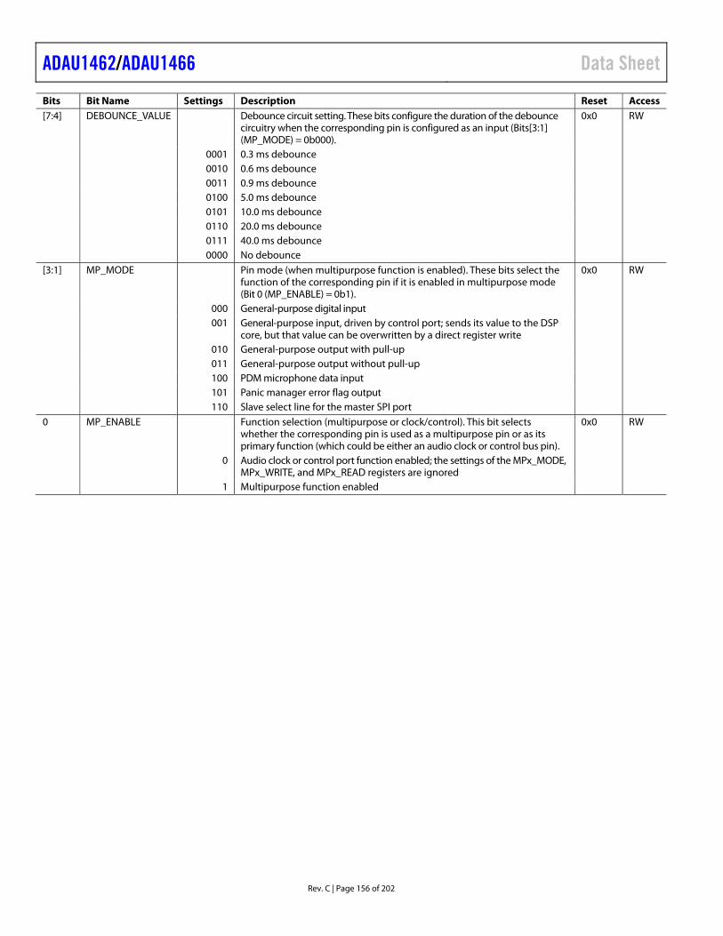
ADAU1462/ADAU1466 Data Sheet
Rev. C | Page 156 of 202
Bits Bit Name Settings Description Reset Access [7:4] DEBOUNCE_VALUE Debounce circuit setting. These bits configure the duration of the debounce
circuitry when the corresponding pin is configured as an input (Bits[3:1] (MP_MODE) = 0b000).
0x0 RW
0001 0.3 ms debounce 0010 0.6 ms debounce 0011 0.9 ms debounce 0100 5.0 ms debounce 0101 10.0 ms debounce 0110 20.0 ms debounce 0111 40.0 ms debounce 0000 No debounce [3:1] MP_MODE Pin mode (when multipurpose function is enabled). These bits select the
function of the corresponding pin if it is enabled in multipurpose mode (Bit 0 (MP_ENABLE) = 0b1).
0x0 RW
000 General-purpose digital input 001 General-purpose input, driven by control port; sends its value to the DSP
core, but that value can be overwritten by a direct register write
010 General-purpose output with pull-up 011 General-purpose output without pull-up 100 PDM microphone data input 101 Panic manager error flag output 110 Slave select line for the master SPI port 0 MP_ENABLE Function selection (multipurpose or clock/control). This bit selects
whether the corresponding pin is used as a multipurpose pin or as its primary function (which could be either an audio clock or control bus pin).
0x0 RW
0 Audio clock or control port function enabled; the settings of the MPx_MODE, MPx_WRITE, and MPx_READ registers are ignored
1 Multipurpose function enabled
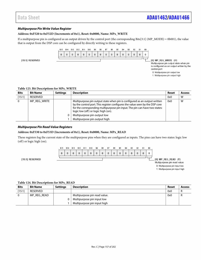
Data Sheet ADAU1462/ADAU1466
Rev. C | Page 157 of 202
Multipurpose Pin Write Value Register
Address: 0xF520 to 0xF52D (Increments of 0x1), Reset: 0x0000, Name: MPx_WRITE
If a multipurpose pin is configured as an output driven by the control port (the corresponding Bits[3:1] (MP_MODE) = 0b001), the value that is output from the DSP core can be configured by directly writing to these registers.
Table 123. Bit Descriptions for MPx_WRITE Bits Bit Name Settings Description Reset Access [15:1] RESERVED 0x0 W 0 MP_REG_WRITE Multipurpose pin output state when pin is configured as an output written
by the control port. This register configures the value seen by the DSP core for the corresponding multipurpose pin input. The pin can have two states: logic low (off ) or logic high (on).
0x0 W
0 Multipurpose pin output low 1 Multipurpose pin output high
Multipurpose Pin Read Value Registers
Address: 0xF530 to 0xF53D (Increments of 0x1), Reset: 0x0000, Name: MPx_READ
These registers log the current state of the multipurpose pins when they are configured as inputs. The pins can have two states: logic low (off) or logic high (on).
Table 124. Bit Descriptions for MPx_READ Bits Bit Name Settings Description Reset Access [15:1] RESERVED 0x0 R 0 MP_REG_READ Multipurpose pin read value. 0x0 R 0 Multipurpose pin input low 1 Multipurpose pin input high
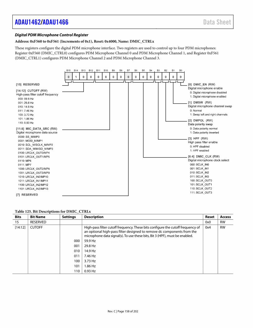
ADAU1462/ADAU1466 Data Sheet
Rev. C | Page 158 of 202
Digital PDM Microphone Control Register
Address: 0xF560 to 0xF561 (Increments of 0x1), Reset: 0x4000, Name: DMIC_CTRLx
These registers configure the digital PDM microphone interface. Two registers are used to control up to four PDM microphones: Register 0xF560 (DMIC_CTRL0) configures PDM Microphone Channel 0 and PDM Microphone Channel 1, and Register 0xF561 (DMIC_CTRL1) configures PDM Microphone Channel 2 and PDM Microphone Channel 3.
Table 125. Bit Descriptions for DMIC_CTRLx Bits Bit Name Settings Description Reset Access 15 RESERVED 0x0 RW [14:12] CUTOFF High-pass filter cutoff frequency. These bits configure the cutoff frequency of
an optional high-pass filter designed to remove dc components from the microphone data signal(s). To use these bits, Bit 3 (HPF), must be enabled.
0x4 RW
000 59.9 Hz 001 29.8 Hz 010 14.9 Hz 011 7.46 Hz 100 3.73 Hz 101 1.86 Hz 110 0.93 Hz
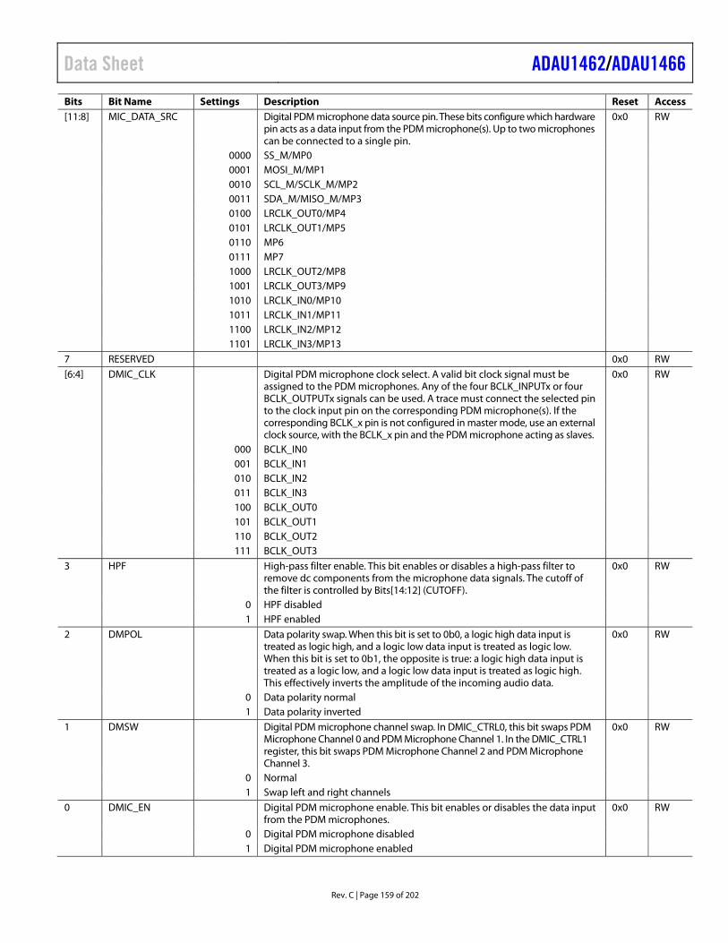
Data Sheet ADAU1462/ADAU1466
Rev. C | Page 159 of 202
Bits Bit Name Settings Description Reset Access [11:8] MIC_DATA_SRC Digital PDM microphone data source pin. These bits configure which hardware
pin acts as a data input from the PDM microphone(s). Up to two microphones can be connected to a single pin.
0x0 RW
0000 SS_M/MP0 0001 MOSI_M/MP1 0010 SCL_M/SCLK_M/MP2 0011 SDA_M/MISO_M/MP3 0100 LRCLK_OUT0/MP4 0101 LRCLK_OUT1/MP5 0110 MP6 0111 MP7 1000 LRCLK_OUT2/MP8 1001 LRCLK_OUT3/MP9 1010 LRCLK_IN0/MP10 1011 LRCLK_IN1/MP11 1100 LRCLK_IN2/MP12 1101 LRCLK_IN3/MP13 7 RESERVED 0x0 RW [6:4] DMIC_CLK Digital PDM microphone clock select. A valid bit clock signal must be
assigned to the PDM microphones. Any of the four BCLK_INPUTx or four BCLK_OUTPUTx signals can be used. A trace must connect the selected pin to the clock input pin on the corresponding PDM microphone(s). If the corresponding BCLK_x pin is not configured in master mode, use an external clock source, with the BCLK_x pin and the PDM microphone acting as slaves.
0x0 RW
000 BCLK_IN0 001 BCLK_IN1 010 BCLK_IN2 011 BCLK_IN3 100 BCLK_OUT0 101 BCLK_OUT1 110 BCLK_OUT2 111 BCLK_OUT3 3 HPF High-pass filter enable. This bit enables or disables a high-pass filter to
remove dc components from the microphone data signals. The cutoff of the filter is controlled by Bits[14:12] (CUTOFF).
0x0 RW
0 HPF disabled 1 HPF enabled 2 DMPOL Data polarity swap. When this bit is set to 0b0, a logic high data input is
treated as logic high, and a logic low data input is treated as logic low. When this bit is set to 0b1, the opposite is true: a logic high data input is treated as a logic low, and a logic low data input is treated as logic high. This effectively inverts the amplitude of the incoming audio data.
0x0 RW
0 Data polarity normal 1 Data polarity inverted 1 DMSW Digital PDM microphone channel swap. In DMIC_CTRL0, this bit swaps PDM
Microphone Channel 0 and PDM Microphone Channel 1. In the DMIC_CTRL1 register, this bit swaps PDM Microphone Channel 2 and PDM Microphone Channel 3.
0x0 RW
0 Normal 1 Swap left and right channels 0 DMIC_EN Digital PDM microphone enable. This bit enables or disables the data input
from the PDM microphones. 0x0 RW
0 Digital PDM microphone disabled 1 Digital PDM microphone enabled
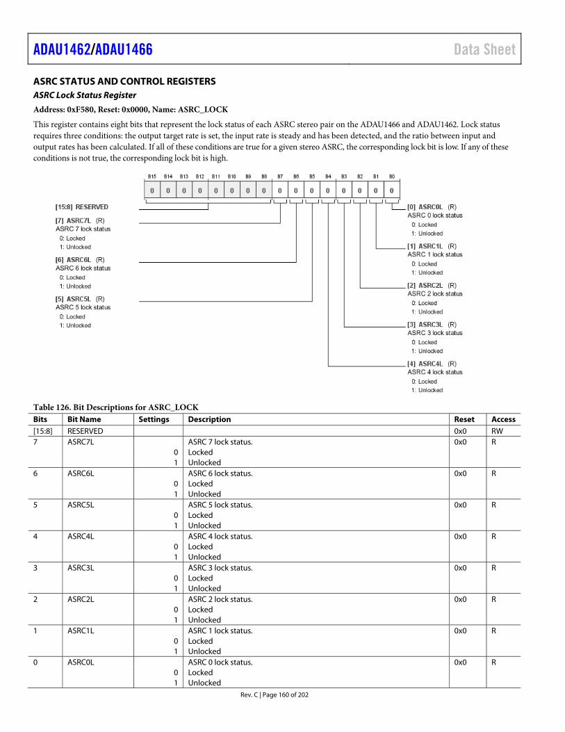
ADAU1462/ADAU1466 Data Sheet
Rev. C | Page 160 of 202
ASRC STATUS AND CONTROL REGISTERS ASRC Lock Status Register
Address: 0xF580, Reset: 0x0000, Name: ASRC_LOCK
This register contains eight bits that represent the lock status of each ASRC stereo pair on the ADAU1466 and ADAU1462. Lock status requires three conditions: the output target rate is set, the input rate is steady and has been detected, and the ratio between input and output rates has been calculated. If all of these conditions are true for a given stereo ASRC, the corresponding lock bit is low. If any of these conditions is not true, the corresponding lock bit is high.
Table 126. Bit Descriptions for ASRC_LOCK Bits Bit Name Settings Description Reset Access [15:8] RESERVED 0x0 RW 7 ASRC7L ASRC 7 lock status. 0x0 R 0 Locked 1 Unlocked 6 ASRC6L ASRC 6 lock status. 0x0 R 0 Locked 1 Unlocked 5 ASRC5L ASRC 5 lock status. 0x0 R 0 Locked 1 Unlocked 4 ASRC4L ASRC 4 lock status. 0x0 R 0 Locked 1 Unlocked 3 ASRC3L ASRC 3 lock status. 0x0 R 0 Locked 1 Unlocked 2 ASRC2L ASRC 2 lock status. 0x0 R 0 Locked 1 Unlocked 1 ASRC1L ASRC 1 lock status. 0x0 R 0 Locked 1 Unlocked 0 ASRC0L ASRC 0 lock status. 0x0 R 0 Locked 1 Unlocked
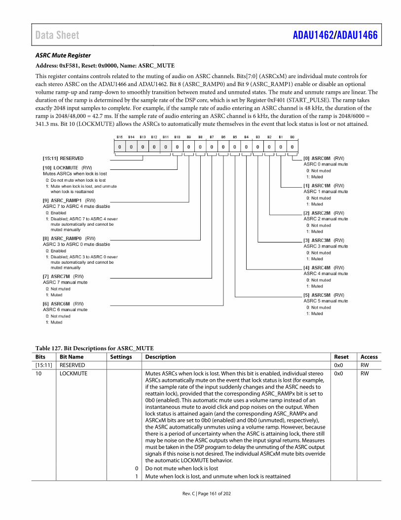
Data Sheet ADAU1462/ADAU1466
Rev. C | Page 161 of 202
ASRC Mute Register
Address: 0xF581, Reset: 0x0000, Name: ASRC_MUTE
This register contains controls related to the muting of audio on ASRC channels. Bits[7:0] (ASRCxM) are individual mute controls for each stereo ASRC on the ADAU1466 and ADAU1462. Bit 8 (ASRC_RAMP0) and Bit 9 (ASRC_RAMP1) enable or disable an optional volume ramp-up and ramp-down to smoothly transition between muted and unmuted states. The mute and unmute ramps are linear. The duration of the ramp is determined by the sample rate of the DSP core, which is set by Register 0xF401 (START_PULSE). The ramp takes exactly 2048 input samples to complete. For example, if the sample rate of audio entering an ASRC channel is 48 kHz, the duration of the ramp is 2048/48,000 = 42.7 ms. If the sample rate of audio entering an ASRC channel is 6 kHz, the duration of the ramp is 2048/6000 = 341.3 ms. Bit 10 (LOCKMUTE) allows the ASRCs to automatically mute themselves in the event that lock status is lost or not attained.
Table 127. Bit Descriptions for ASRC_MUTE Bits Bit Name Settings Description Reset Access [15:11] RESERVED 0x0 RW 10 LOCKMUTE Mutes ASRCs when lock is lost. When this bit is enabled, individual stereo
ASRCs automatically mute on the event that lock status is lost (for example, if the sample rate of the input suddenly changes and the ASRC needs to reattain lock), provided that the corresponding ASRC_RAMPx bit is set to 0b0 (enabled). This automatic mute uses a volume ramp instead of an instantaneous mute to avoid click and pop noises on the output. When lock status is attained again (and the corresponding ASRC_RAMPx and ASRCxM bits are set to 0b0 (enabled) and 0b0 (unmuted), respectively), the ASRC automatically unmutes using a volume ramp. However, because there is a period of uncertainty when the ASRC is attaining lock, there still may be noise on the ASRC outputs when the input signal returns. Measures must be taken in the DSP program to delay the unmuting of the ASRC output signals if this noise is not desired. The individual ASRCxM mute bits override the automatic LOCKMUTE behavior.
0x0 RW
0 Do not mute when lock is lost 1 Mute when lock is lost, and unmute when lock is reattained
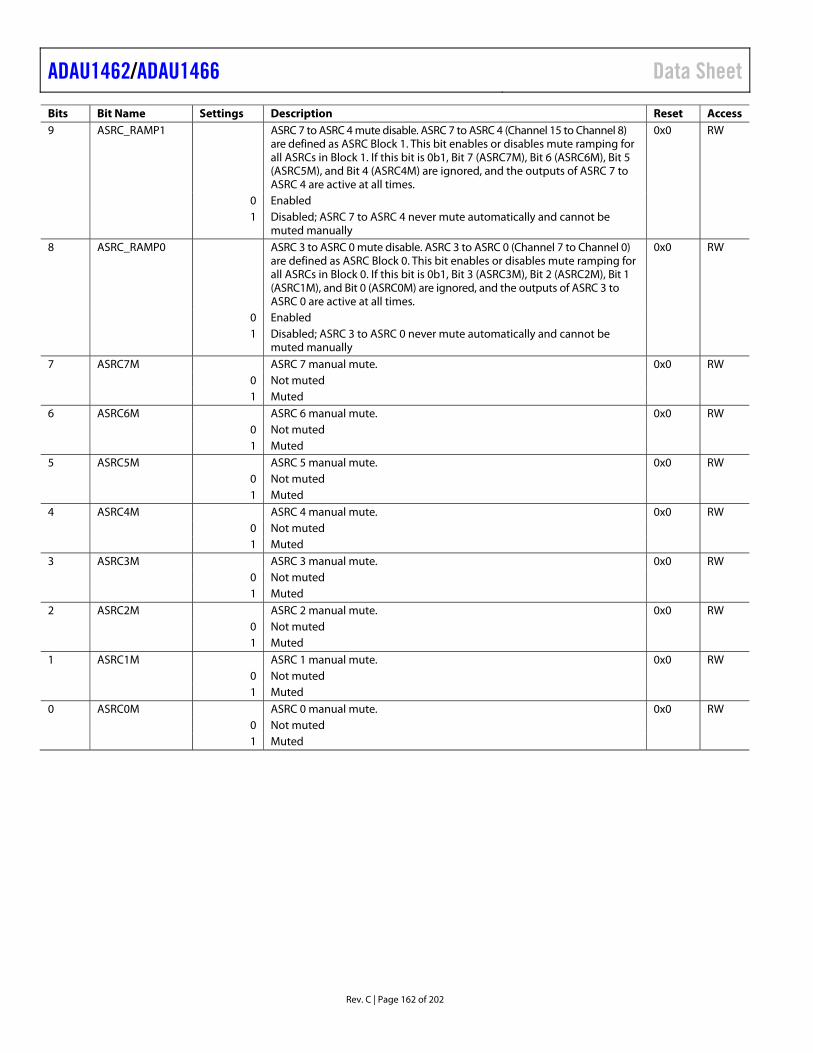
ADAU1462/ADAU1466 Data Sheet
Rev. C | Page 162 of 202
Bits Bit Name Settings Description Reset Access 9 ASRC_RAMP1 ASRC 7 to ASRC 4 mute disable. ASRC 7 to ASRC 4 (Channel 15 to Channel 8)
are defined as ASRC Block 1. This bit enables or disables mute ramping for all ASRCs in Block 1. If this bit is 0b1, Bit 7 (ASRC7M), Bit 6 (ASRC6M), Bit 5 (ASRC5M), and Bit 4 (ASRC4M) are ignored, and the outputs of ASRC 7 to ASRC 4 are active at all times.
0x0 RW
0 Enabled 1 Disabled; ASRC 7 to ASRC 4 never mute automatically and cannot be
muted manually
8 ASRC_RAMP0 ASRC 3 to ASRC 0 mute disable. ASRC 3 to ASRC 0 (Channel 7 to Channel 0) are defined as ASRC Block 0. This bit enables or disables mute ramping for all ASRCs in Block 0. If this bit is 0b1, Bit 3 (ASRC3M), Bit 2 (ASRC2M), Bit 1 (ASRC1M), and Bit 0 (ASRC0M) are ignored, and the outputs of ASRC 3 to ASRC 0 are active at all times.
0x0 RW
0 Enabled 1 Disabled; ASRC 3 to ASRC 0 never mute automatically and cannot be
muted manually
7 ASRC7M ASRC 7 manual mute. 0x0 RW 0 Not muted 1 Muted 6 ASRC6M ASRC 6 manual mute. 0x0 RW 0 Not muted 1 Muted 5 ASRC5M ASRC 5 manual mute. 0x0 RW 0 Not muted 1 Muted 4 ASRC4M ASRC 4 manual mute. 0x0 RW 0 Not muted 1 Muted 3 ASRC3M ASRC 3 manual mute. 0x0 RW 0 Not muted 1 Muted 2 ASRC2M ASRC 2 manual mute. 0x0 RW 0 Not muted 1 Muted 1 ASRC1M ASRC 1 manual mute. 0x0 RW 0 Not muted 1 Muted 0 ASRC0M ASRC 0 manual mute. 0x0 RW 0 Not muted 1 Muted
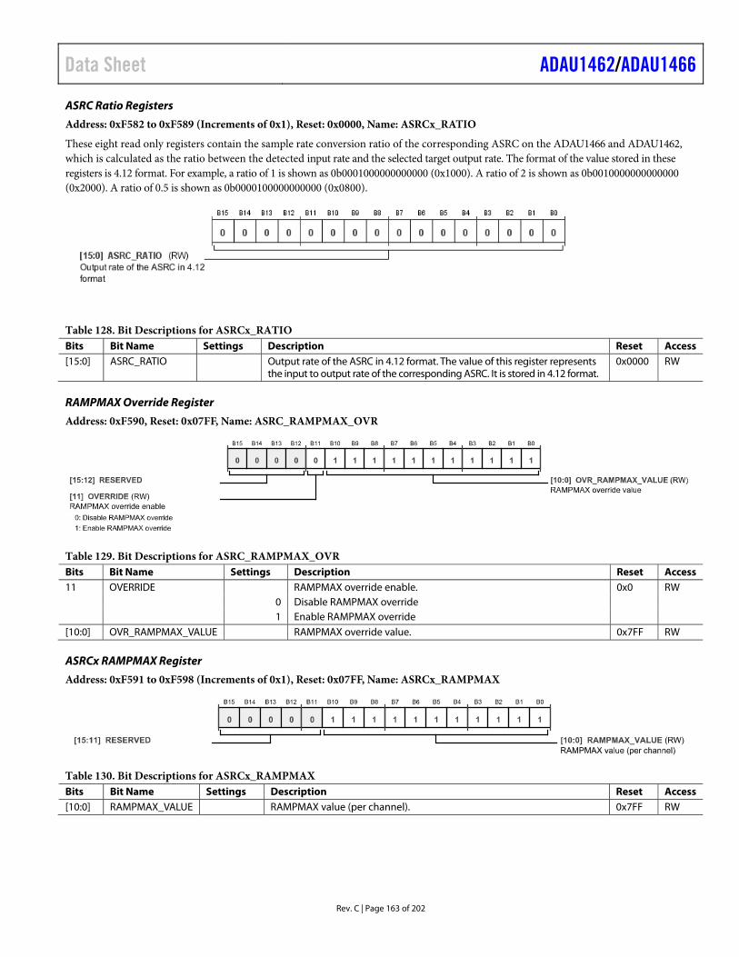
Data Sheet ADAU1462/ADAU1466
Rev. C | Page 163 of 202
ASRC Ratio Registers
Address: 0xF582 to 0xF589 (Increments of 0x1), Reset: 0x0000, Name: ASRCx_RATIO
These eight read only registers contain the sample rate conversion ratio of the corresponding ASRC on the ADAU1466 and ADAU1462, which is calculated as the ratio between the detected input rate and the selected target output rate. The format of the value stored in these registers is 4.12 format. For example, a ratio of 1 is shown as 0b0001000000000000 (0x1000). A ratio of 2 is shown as 0b0010000000000000 (0x2000). A ratio of 0.5 is shown as 0b0000100000000000 (0x0800).
Table 128. Bit Descriptions for ASRCx_RATIO Bits Bit Name Settings Description Reset Access [15:0] ASRC_RATIO Output rate of the ASRC in 4.12 format. The value of this register represents
the input to output rate of the corresponding ASRC. It is stored in 4.12 format. 0x0000 RW
RAMPMAX Override Register
Address: 0xF590, Reset: 0x07FF, Name: ASRC_RAMPMAX_OVR
Table 129. Bit Descriptions for ASRC_RAMPMAX_OVR Bits Bit Name Settings Description Reset Access 11 OVERRIDE RAMPMAX override enable. 0x0 RW 0 Disable RAMPMAX override 1 Enable RAMPMAX override [10:0] OVR_RAMPMAX_VALUE RAMPMAX override value. 0x7FF RW
ASRCx RAMPMAX Register
Address: 0xF591 to 0xF598 (Increments of 0x1), Reset: 0x07FF, Name: ASRCx_RAMPMAX
Table 130. Bit Descriptions for ASRCx_RAMPMAX Bits Bit Name Settings Description Reset Access [10:0] RAMPMAX_VALUE RAMPMAX value (per channel). 0x7FF RW
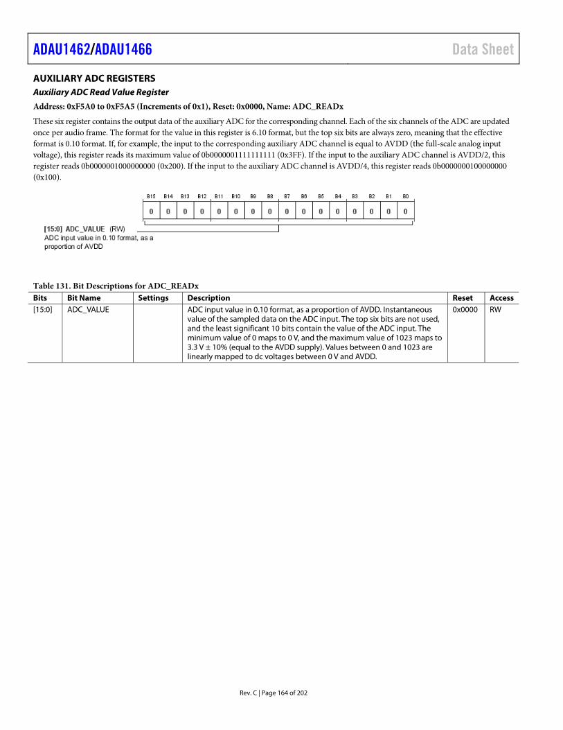
ADAU1462/ADAU1466 Data Sheet
Rev. C | Page 164 of 202
AUXILIARY ADC REGISTERS Auxiliary ADC Read Value Register
Address: 0xF5A0 to 0xF5A5 (Increments of 0x1), Reset: 0x0000, Name: ADC_READx
These six register contains the output data of the auxiliary ADC for the corresponding channel. Each of the six channels of the ADC are updated once per audio frame. The format for the value in this register is 6.10 format, but the top six bits are always zero, meaning that the effective format is 0.10 format. If, for example, the input to the corresponding auxiliary ADC channel is equal to AVDD (the full-scale analog input voltage), this register reads its maximum value of 0b0000001111111111 (0x3FF). If the input to the auxiliary ADC channel is AVDD/2, this register reads 0b0000001000000000 (0x200). If the input to the auxiliary ADC channel is AVDD/4, this register reads 0b0000000100000000 (0x100).
Table 131. Bit Descriptions for ADC_READx Bits Bit Name Settings Description Reset Access [15:0] ADC_VALUE ADC input value in 0.10 format, as a proportion of AVDD. Instantaneous
value of the sampled data on the ADC input. The top six bits are not used, and the least significant 10 bits contain the value of the ADC input. The minimum value of 0 maps to 0 V, and the maximum value of 1023 maps to 3.3 V ± 10% (equal to the AVDD supply). Values between 0 and 1023 are linearly mapped to dc voltages between 0 V and AVDD.
0x0000 RW
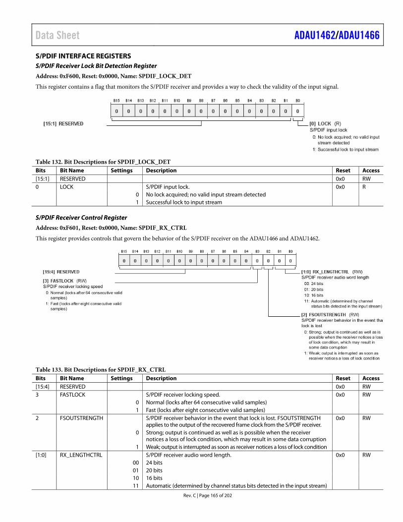
Data Sheet ADAU1462/ADAU1466
Rev. C | Page 165 of 202
S/PDIF INTERFACE REGISTERS S/PDIF Receiver Lock Bit Detection Register
Address: 0xF600, Reset: 0x0000, Name: SPDIF_LOCK_DET
This register contains a flag that monitors the S/PDIF receiver and provides a way to check the validity of the input signal.
Table 132. Bit Descriptions for SPDIF_LOCK_DET Bits Bit Name Settings Description Reset Access [15:1] RESERVED 0x0 RW 0 LOCK S/PDIF input lock. 0x0 R 0 No lock acquired; no valid input stream detected 1 Successful lock to input stream
S/PDIF Receiver Control Register
Address: 0xF601, Reset: 0x0000, Name: SPDIF_RX_CTRL
This register provides controls that govern the behavior of the S/PDIF receiver on the ADAU1466 and ADAU1462.
Table 133. Bit Descriptions for SPDIF_RX_CTRL Bits Bit Name Settings Description Reset Access [15:4] RESERVED 0x0 RW 3 FASTLOCK S/PDIF receiver locking speed. 0x0 RW 0 Normal (locks after 64 consecutive valid samples) 1 Fast (locks after eight consecutive valid samples) 2 FSOUTSTRENGTH S/PDIF receiver behavior in the event that lock is lost. FSOUTSTRENGTH
applies to the output of the recovered frame clock from the S/PDIF receiver. 0x0 RW
0 Strong; output is continued as well as is possible when the receiver notices a loss of lock condition, which may result in some data corruption
1 Weak; output is interrupted as soon as receiver notices a loss of lock condition [1:0] RX_LENGTHCTRL S/PDIF receiver audio word length. 0x0 RW 00 24 bits 01 20 bits 10 16 bits 11 Automatic (determined by channel status bits detected in the input stream)
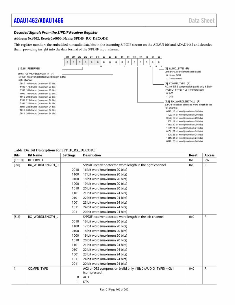
ADAU1462/ADAU1466 Data Sheet
Rev. C | Page 166 of 202
Decoded Signals From the S/PDIF Receiver Register
Address: 0xF602, Reset: 0x0000, Name: SPDIF_RX_DECODE
This register monitors the embedded nonaudio data bits in the incoming S/PDIF stream on the ADAU1466 and ADAU1462 and decodes them, providing insight into the data format of the S/PDIF input stream.
Table 134. Bit Descriptions for SPDIF_RX_DECODE Bits Bit Name Settings Description Reset Access [15:10] RESERVED 0x0 RW [9:6] RX_WORDLENGTH_R S/PDIF receiver detected word length in the right channel. 0x0 R 0010 16 bit word (maximum 20 bits) 1100 17 bit word (maximum 20 bits) 0100 18 bit word (maximum 20 bits) 1000 19 bit word (maximum 20 bits) 1010 20 bit word (maximum 20 bits) 1101 21 bit word (maximum 24 bits) 0101 22 bit word (maximum 24 bits) 1001 23 bit word (maximum 24 bits) 1011 24 bit word (maximum 24 bits) 0011 20 bit word (maximum 24 bits) [5:2] RX_WORDLENGTH_L S/PDIF receiver detected word length in the left channel. 0x0 R 0010 16 bit word (maximum 20 bits) 1100 17 bit word (maximum 20 bits) 0100 18 bit word (maximum 20 bits) 1000 19 bit word (maximum 20 bits) 1010 20 bit word (maximum 20 bits) 1101 21 bit word (maximum 24 bits) 0101 22 bit word (maximum 24 bits) 1001 23 bit word (maximum 24 bits) 1011 24 bit word (maximum 24 bits) 0011 20 bit word (maximum 24 bits) 1 COMPR_TYPE AC3 or DTS compression (valid only if Bit 0 (AUDIO_TYPE) = 0b1
(compressed). 0x0 R
0 AC3 1 DTS
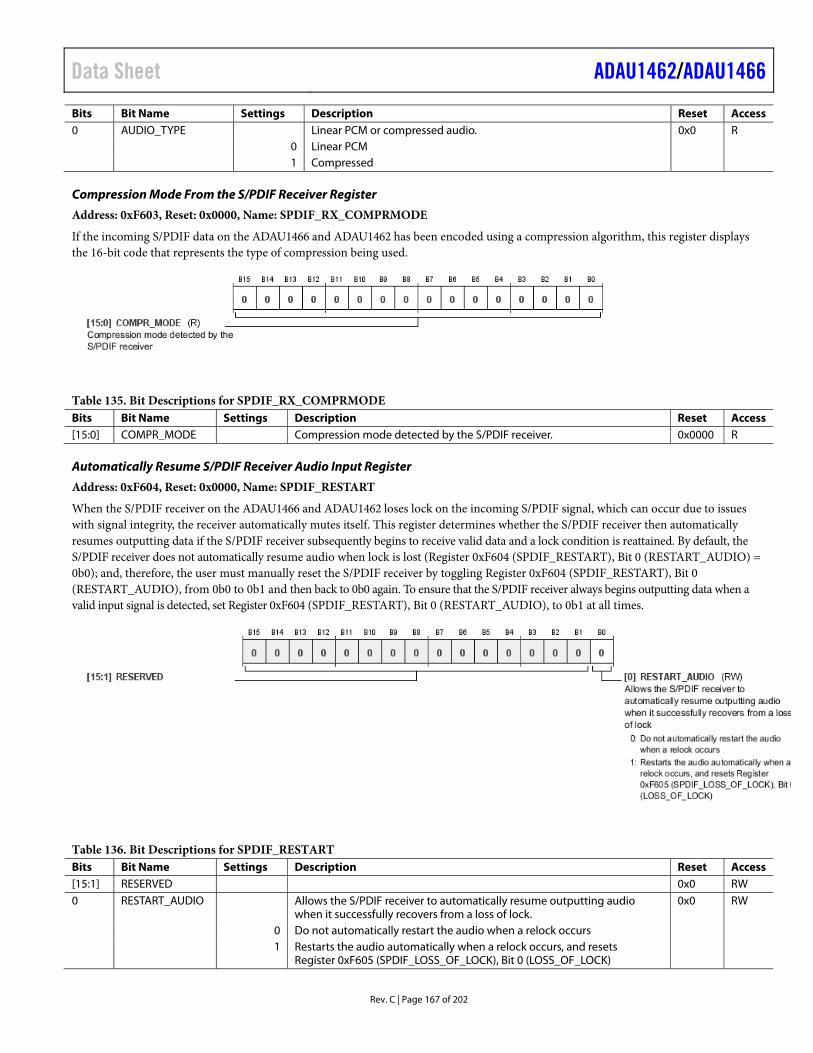
Data Sheet ADAU1462/ADAU1466
Rev. C | Page 167 of 202
Bits Bit Name Settings Description Reset Access 0 AUDIO_TYPE Linear PCM or compressed audio. 0x0 R 0 Linear PCM 1 Compressed
Compression Mode From the S/PDIF Receiver Register
Address: 0xF603, Reset: 0x0000, Name: SPDIF_RX_COMPRMODE
If the incoming S/PDIF data on the ADAU1466 and ADAU1462 has been encoded using a compression algorithm, this register displays the 16-bit code that represents the type of compression being used.
Table 135. Bit Descriptions for SPDIF_RX_COMPRMODE Bits Bit Name Settings Description Reset Access [15:0] COMPR_MODE Compression mode detected by the S/PDIF receiver. 0x0000 R
Automatically Resume S/PDIF Receiver Audio Input Register
Address: 0xF604, Reset: 0x0000, Name: SPDIF_RESTART
When the S/PDIF receiver on the ADAU1466 and ADAU1462 loses lock on the incoming S/PDIF signal, which can occur due to issues with signal integrity, the receiver automatically mutes itself. This register determines whether the S/PDIF receiver then automatically resumes outputting data if the S/PDIF receiver subsequently begins to receive valid data and a lock condition is reattained. By default, the S/PDIF receiver does not automatically resume audio when lock is lost (Register 0xF604 (SPDIF_RESTART), Bit 0 (RESTART_AUDIO) = 0b0); and, therefore, the user must manually reset the S/PDIF receiver by toggling Register 0xF604 (SPDIF_RESTART), Bit 0 (RESTART_AUDIO), from 0b0 to 0b1 and then back to 0b0 again. To ensure that the S/PDIF receiver always begins outputting data when a valid input signal is detected, set Register 0xF604 (SPDIF_RESTART), Bit 0 (RESTART_AUDIO), to 0b1 at all times.
Table 136. Bit Descriptions for SPDIF_RESTART Bits Bit Name Settings Description Reset Access [15:1] RESERVED 0x0 RW 0 RESTART_AUDIO Allows the S/PDIF receiver to automatically resume outputting audio
when it successfully recovers from a loss of lock. 0x0 RW
0 Do not automatically restart the audio when a relock occurs 1 Restarts the audio automatically when a relock occurs, and resets
Register 0xF605 (SPDIF_LOSS_OF_LOCK), Bit 0 (LOSS_OF_LOCK)
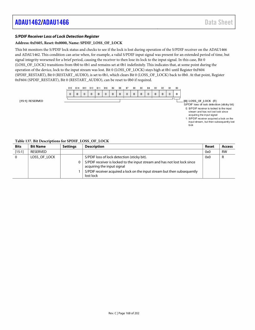
ADAU1462/ADAU1466 Data Sheet
Rev. C | Page 168 of 202
S/PDIF Receiver Loss of Lock Detection Register
Address: 0xF605, Reset: 0x0000, Name: SPDIF_LOSS_OF_LOCK
This bit monitors the S/PDIF lock status and checks to see if the lock is lost during operation of the S/PDIF receiver on the ADAU1466 and ADAU1462. This condition can arise when, for example, a valid S/PDIF input signal was present for an extended period of time, but signal integrity worsened for a brief period, causing the receiver to then lose its lock to the input signal. In this case, Bit 0 (LOSS_OF_LOCK) transitions from 0b0 to 0b1 and remains set at 0b1 indefinitely. This indicates that, at some point during the operation of the device, lock to the input stream was lost. Bit 0 (LOSS_OF_LOCK) stays high at 0b1 until Register 0xF604 (SPDIF_RESTART), Bit 0 (RESTART_AUDIO), is set to 0b1, which clears Bit 0 (LOSS_OF_LOCK) back to 0b0. At that point, Register 0xF604 (SPDIF_RESTART), Bit 0 (RESTART_AUDIO), can be reset to 0b0 if required.
Table 137. Bit Descriptions for SPDIF_LOSS_OF_LOCK Bits Bit Name Settings Description Reset Access [15:1] RESERVED 0x0 RW 0 LOSS_OF_LOCK S/PDIF loss of lock detection (sticky bit). 0x0 R 0 S/PDIF receiver is locked to the input stream and has not lost lock since
acquiring the input signal
1 S/PDIF receiver acquired a lock on the input stream but then subsequently lost lock
Data Sheet ADAU1462/ADAU1466
Rev. C | Page 169 of 202
S/PDIF Receiver Auxiliary Outputs Enable Register
Address: 0xF608, Reset: 0x0000, Name: SPDIF_AUX_EN
The S/PDIF receiver on the ADAU1466 and ADAU1462 decodes embedded nonaudio data bits on the incoming data stream, including channel status, user data, validity bits, and parity bits. This information, together with the decoded audio data, can optionally be output on one of the SDATA_OUTx pins using Register 0xF608 (SPDIF_AUX_EN). The serial output port selected by Bits[3:0] (TDMOUT) outputs an 8-channel TDM stream containing this decoded information.
Channel 0 in the TDM8 stream contains the 24 audio bits from the left S/PDIF input channel, followed by eight zero bits.
Channel 1 in the TDM8 stream contains 20 zero bits, the parity bit, validity bit, user data bit, and the channel status bit from the left S/PDIF input channel, followed by eight zero bits.
Channel 2 in the TDM8 stream contains 22 zero bits, followed by the compression type bit (0b0 represents AC3 and 0b1 represents DTS) and the audio type bit (0b0 represents PCM and 0b1 represents compressed), followed by eight zero bits.
Channel 3 in the TDM8 stream contains 32 zero bits.
Channel 4 in the TDM8 stream contains the 24 audio bits from the right S/PDIF input channel, followed by eight zero bits.
Channel 5 in the TDM8 stream contains 20 zero bits followed by the parity bit, validity bit, user data bit, and channel status bit from the right S/PDIF input channel, followed by eight zero bits.
Channel 6 in the TDM8 stream contains 32 zero bits.
Channel 7 in the TDM8 stream contains 23 zero bits, the block start bit, and eight zero bits.
Table 138. Bit Descriptions for SPDIF_AUX_EN Bits Bit Name Settings Description Reset Access [15:5] RESERVED 0x0 RW 4 TDMOUT_CLK S/PDIF TDM clock source. When Bits[3:0] (TDMOUT) are configured to output S/PDIF
receiver data on one of the SDATA_OUTx pins, the corresponding serial port must be set in master mode; and Bit 4 (TDMOUT_CLK) configures which clock signals are used on the corresponding BCLK_OUTx and LRCLK_OUTx pins. If Bit 4 (TDMOUT_CLK) = 0b0, the clock signals recovered from the S/PDIF input signal are used to clock the serial output. If Bit 4 (TDMOUT_CLK) = 0b1, the output of Clock Generator 3 is used to clock serial output; and Register 0xF026 (CLK_GEN3_SRC), Bits[3:0] (FREF_PIN), must be 0b1110, and Register 0xF026 (CLK_GEN3_SRC), Bit 4 (CLK_GEN3_SRC), must be 0b1.
0x0 RW
0 Use clocks derived from S/PDIF receiver stream 1 Use filtered clocks from internal clock generator [3:0] TDMOUT S/PDIF TDM output channel selection. 0x0 RW 0001 Output on SDATA_OUT0 0010 Output on SDATA_OUT1 0100 Output on SDATA_OUT2 1000 Output on SDATA_OUT3 0000 Disable S/PDIF TDM output
ADAU1462/ADAU1466 Data Sheet
Rev. C | Page 170 of 202
S/PDIF Receiver Auxiliary Bits Ready Flag Register
Address: 0xF60F, Reset: 0x0000, Name: SPDIF_RX_AUXBIT_READY
The decoded channel status, user data, validity, and parity bits are recovered from the input signal one frame at a time until a full block of 192 frames is received on the ADAU1466 and ADAU1462. When all of the 192 frames are received and decoded, Bit 0 (AUXBITS_READY), changes state from 0b0 to 0b1, indicating that the full block of data has been recovered and is available to be read from the corresponding registers.
Table 139. Bit Descriptions for SPDIF_RX_AUXBIT_READY Bits Bit Name Settings Description Reset Access [15:1] RESERVED 0x0 RW 0 AUXBITS_READY Auxiliary bits are ready flag. 0x0 R 0 Auxiliary bits are not ready to be output 1 Auxiliary bits are ready to be output
S/PDIF Receiver Channel Status Bits (Left) Register
Address: 0xF610 to 0xF61B (Increments of 0x1), Reset: 0x0000, Name: SPDIF_RX_CS_LEFT_x
These 12 registers store the 192 channel status bits decoded from the left channel of the S/PDIF input stream on the ADAU1466 and ADAU1462.
Table 140. Bit Descriptions for SPDIF_RX_CS_LEFT_x Bits Bit Name Settings Description Reset Access [15:0] SPDIF_RX_CS_LEFT S/PDIF receiver channel status bits (left). 0x0000 R
S/PDIF Receiver Channel Status Bits (Right) Register
Address: 0xF620 to 0xF62B (Increments of 0x1), Reset: 0x0000, Name: SPDIF_RX_CS_RIGHT_x
These 12 registers store the 192 channel status bits decoded from the right channel of the S/PDIF input stream on the ADAU1466 and ADAU1462.
Table 141. Bit Descriptions for SPDIF_RX_CS_RIGHT_x Bits Bit Name Settings Description Reset Access [15:0] SPDIF_RX_CS_RIGHT S/PDIF receiver channel status bits (right). 0x0000 R
Data Sheet ADAU1462/ADAU1466
Rev. C | Page 171 of 202
S/PDIF Receiver User Data Bits (Left) Register
Address: 0xF630 to 0xF63B (Increments of 0x1), Reset: 0x0000, Name: SPDIF_RX_UD_LEFT_x
These 12 registers store the 192 user data bits decoded from the left channel of the S/PDIF input stream on the ADAU1466 and ADAU1462.
Table 142. Bit Descriptions for SPDIF_RX_UD_LEFT_x Bits Bit Name Settings Description Reset Access [15:0] SPDIF_RX_UD_LEFT S/PDIF receiver user data bits (left). 0x0000 R
S/PDIF Receiver User Data Bits (Right) Register
Address: 0xF640 to 0xF64B (Increments of 0x1), Reset: 0x0000, Name: SPDIF_RX_UD_RIGHT_x
These 12 registers store the 192 user data bits decoded from the right channel of the S/PDIF input stream on the ADAU1466 and ADAU1462.
Table 143. Bit Descriptions for SPDIF_RX_UD_RIGHT_x Bits Bit Name Settings Description Reset Access [15:0] SPDIF_RX_UD_RIGHT S/PDIF receiver user data bits (right). 0x0000 R
S/PDIF Receiver Validity Bits (Left) Register
Address: 0xF650 to 0xF65B (Increments of 0x1), Reset: 0x0000, Name: SPDIF_RX_VB_LEFT_x
These 12 registers store the 192 validity bits decoded from the left channel of the S/PDIF input stream on the ADAU1466 and ADAU1462.
Table 144. Bit Descriptions for SPDIF_RX_VB_LEFT_x Bits Bit Name Settings Description Reset Access [15:0] SPDIF_RX_VB_LEFT S/PDIF receiver validity bits (left). 0x0000 R
ADAU1462/ADAU1466 Data Sheet
Rev. C | Page 172 of 202
S/PDIF Receiver Validity Bits (Right) Register
Address: 0xF660 to 0xF66B (Increments of 0x1), Reset: 0x0000, Name: SPDIF_RX_VB_RIGHT_x
These 12 registers store the 192 validity bits decoded from the left channel of the S/PDIF input stream on the ADAU1466 and ADAU1462.
Table 145. Bit Descriptions for SPDIF_RX_VB_RIGHT_x Bits Bit Name Settings Description Reset Access [15:0] SPDIF_RX_VB_RIGHT S/PDIF receiver validity bits (right). 0x0000 R
S/PDIF Receiver Parity Bits (Left) Register
Address: 0xF670 to 0xF67B (Increments of 0x1), Reset: 0x0000, Name: SPDIF_RX_PB_LEFT_x
These 12 registers store the 192 parity bits decoded from the left channel of the S/PDIF input stream on the ADAU1466 and ADAU1462.
Table 146. Bit Descriptions for SPDIF_RX_PB_LEFT_x Bits Bit Name Settings Description Reset Access [15:0] SPDIF_RX_PB_LEFT S/PDIF receiver parity bits (left). 0x0000 R
S/PDIF Receiver Parity Bits (Right) Register
Address: 0xF680 to 0xF68B (Increments of 0x1), Reset: 0x0000, Name: SPDIF_RX_PB_RIGHT_x
These 12 registers store the 192 parity bits decoded from the right channel of the S/PDIF input stream on the ADAU1466 and ADAU1462.
Table 147. Bit Descriptions for SPDIF_RX_PB_RIGHT_x Bits Bit Name Settings Description Reset Access [15:0] SPDIF_RX_PB_RIGHT S/PDIF receiver parity bits (right). 0x0000 R
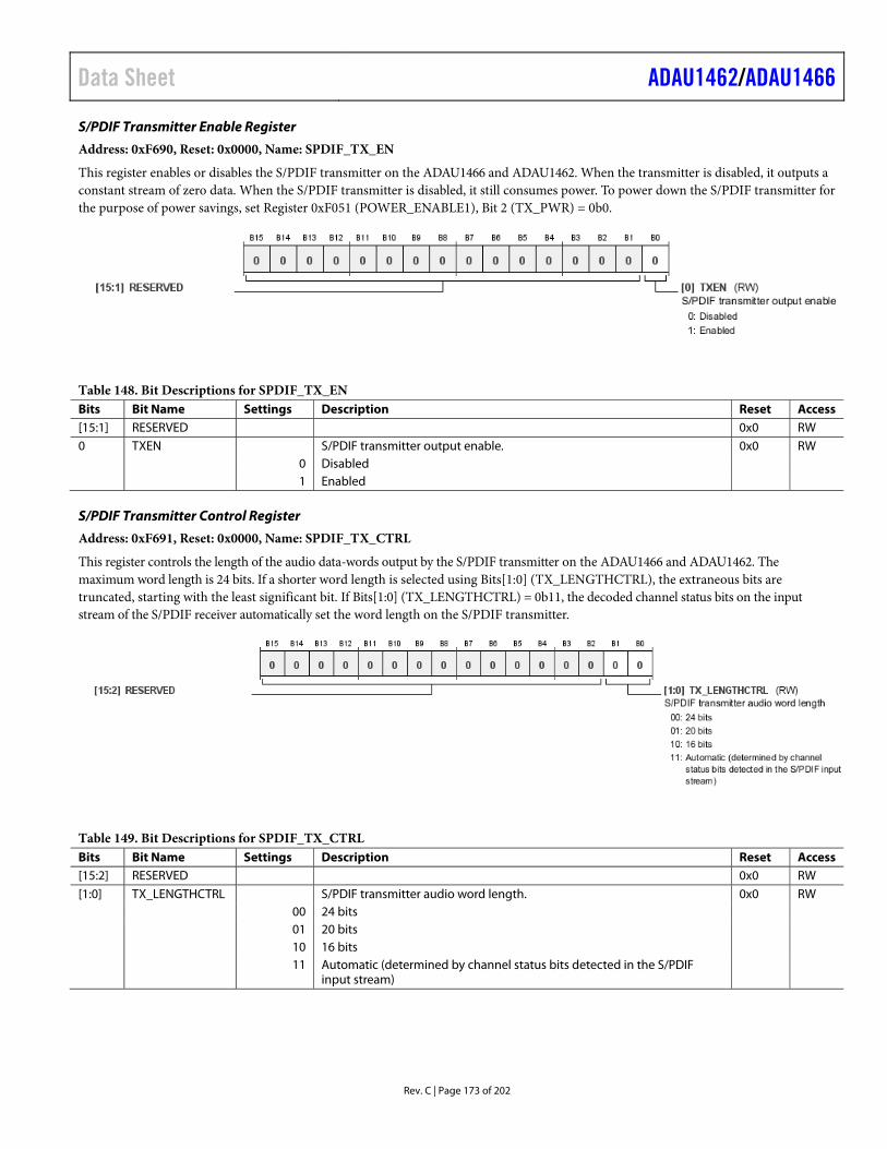
Data Sheet ADAU1462/ADAU1466
Rev. C | Page 173 of 202
S/PDIF Transmitter Enable Register
Address: 0xF690, Reset: 0x0000, Name: SPDIF_TX_EN
This register enables or disables the S/PDIF transmitter on the ADAU1466 and ADAU1462. When the transmitter is disabled, it outputs a constant stream of zero data. When the S/PDIF transmitter is disabled, it still consumes power. To power down the S/PDIF transmitter for the purpose of power savings, set Register 0xF051 (POWER_ENABLE1), Bit 2 (TX_PWR) = 0b0.
Table 148. Bit Descriptions for SPDIF_TX_EN Bits Bit Name Settings Description Reset Access [15:1] RESERVED 0x0 RW 0 TXEN S/PDIF transmitter output enable. 0x0 RW 0 Disabled 1 Enabled
S/PDIF Transmitter Control Register
Address: 0xF691, Reset: 0x0000, Name: SPDIF_TX_CTRL
This register controls the length of the audio data-words output by the S/PDIF transmitter on the ADAU1466 and ADAU1462. The maximum word length is 24 bits. If a shorter word length is selected using Bits[1:0] (TX_LENGTHCTRL), the extraneous bits are truncated, starting with the least significant bit. If Bits[1:0] (TX_LENGTHCTRL) = 0b11, the decoded channel status bits on the input stream of the S/PDIF receiver automatically set the word length on the S/PDIF transmitter.
Table 149. Bit Descriptions for SPDIF_TX_CTRL Bits Bit Name Settings Description Reset Access [15:2] RESERVED 0x0 RW [1:0] TX_LENGTHCTRL S/PDIF transmitter audio word length. 0x0 RW 00 24 bits 01 20 bits 10 16 bits 11 Automatic (determined by channel status bits detected in the S/PDIF
input stream)
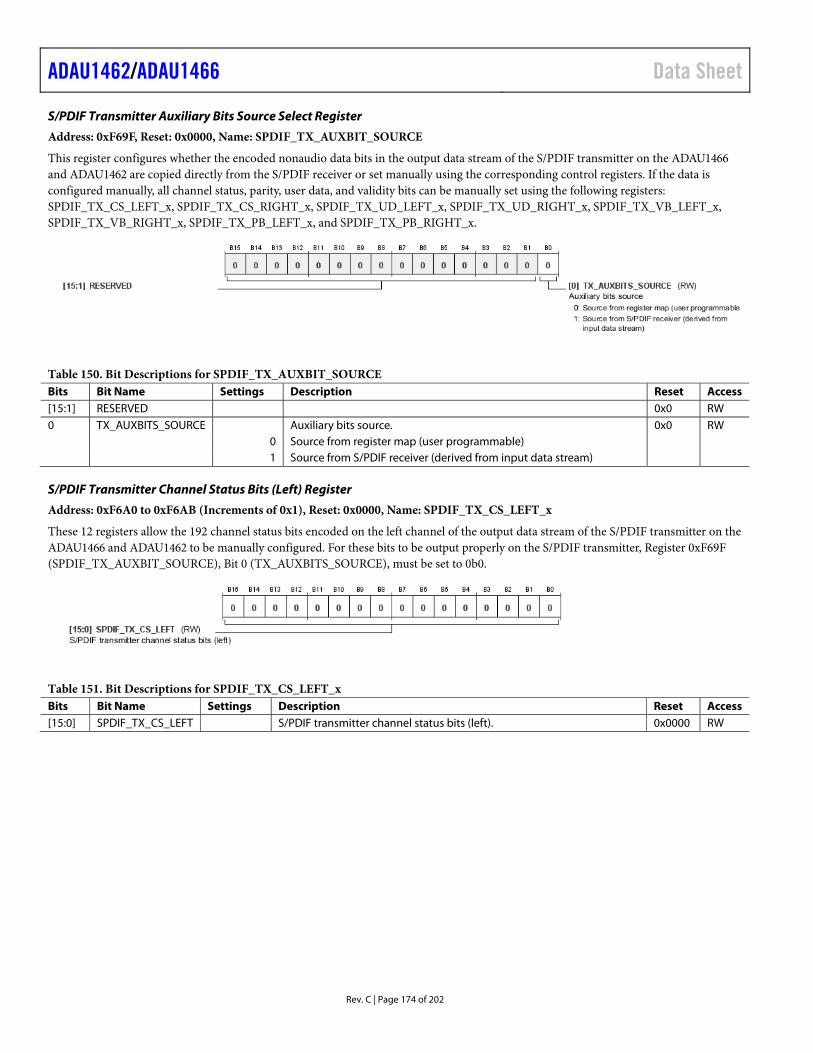
ADAU1462/ADAU1466 Data Sheet
Rev. C | Page 174 of 202
S/PDIF Transmitter Auxiliary Bits Source Select Register
Address: 0xF69F, Reset: 0x0000, Name: SPDIF_TX_AUXBIT_SOURCE
This register configures whether the encoded nonaudio data bits in the output data stream of the S/PDIF transmitter on the ADAU1466 and ADAU1462 are copied directly from the S/PDIF receiver or set manually using the corresponding control registers. If the data is configured manually, all channel status, parity, user data, and validity bits can be manually set using the following registers: SPDIF_TX_CS_LEFT_x, SPDIF_TX_CS_RIGHT_x, SPDIF_TX_UD_LEFT_x, SPDIF_TX_UD_RIGHT_x, SPDIF_TX_VB_LEFT_x, SPDIF_TX_VB_RIGHT_x, SPDIF_TX_PB_LEFT_x, and SPDIF_TX_PB_RIGHT_x.
Table 150. Bit Descriptions for SPDIF_TX_AUXBIT_SOURCE Bits Bit Name Settings Description Reset Access [15:1] RESERVED 0x0 RW 0 TX_AUXBITS_SOURCE Auxiliary bits source. 0x0 RW 0 Source from register map (user programmable) 1 Source from S/PDIF receiver (derived from input data stream)
S/PDIF Transmitter Channel Status Bits (Left) Register
Address: 0xF6A0 to 0xF6AB (Increments of 0x1), Reset: 0x0000, Name: SPDIF_TX_CS_LEFT_x
These 12 registers allow the 192 channel status bits encoded on the left channel of the output data stream of the S/PDIF transmitter on the ADAU1466 and ADAU1462 to be manually configured. For these bits to be output properly on the S/PDIF transmitter, Register 0xF69F (SPDIF_TX_AUXBIT_SOURCE), Bit 0 (TX_AUXBITS_SOURCE), must be set to 0b0.
Table 151. Bit Descriptions for SPDIF_TX_CS_LEFT_x Bits Bit Name Settings Description Reset Access [15:0] SPDIF_TX_CS_LEFT S/PDIF transmitter channel status bits (left). 0x0000 RW
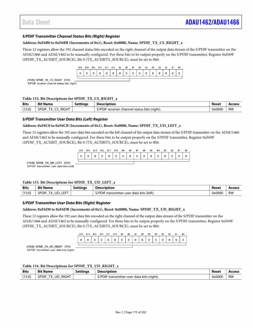
Data Sheet ADAU1462/ADAU1466
Rev. C | Page 175 of 202
S/PDIF Transmitter Channel Status Bits (Right) Register
Address: 0xF6B0 to 0xF6BB (Increments of 0x1), Reset: 0x0000, Name: SPDIF_TX_CS_RIGHT_x
These 12 registers allow the 192 channel status bits encoded on the right channel of the output data stream of the S/PDIF transmitter on the ADAU1466 and ADAU1462 to be manually configured. For these bits to be output properly on the S/PDIF transmitter, Register 0xF69F (SPDIF_TX_AUXBIT_SOURCE), Bit 0 (TX_AUXBITS_SOURCE), must be set to 0b0.
Table 152. Bit Descriptions for SPDIF_TX_CS_RIGHT_x Bits Bit Name Settings Description Reset Access [15:0] SPDIF_TX_CS_RIGHT S/PDIF receiver channel status bits (right). 0x0000 RW
S/PDIF Transmitter User Data Bits (Left) Register
Address: 0xF6C0 to 0xF6CB (Increments of 0x1), Reset: 0x0000, Name: SPDIF_TX_UD_LEFT_x
These 12 registers allow the 192 user data bits encoded on the left channel of the output data stream of the S/PDIF transmitter on the ADAU1466 and ADAU1462 to be manually configured. For these bits to be output properly on the S/PDIF transmitter, Register 0xF69F (SPDIF_TX_AUXBIT_SOURCE), Bit 0 (TX_AUXBITS_SOURCE), must be set to 0b0.
Table 153. Bit Descriptions for SPDIF_TX_UD_LEFT_x Bits Bit Name Settings Description Reset Access [15:0] SPDIF_TX_UD_LEFT S/PDIF transmitter user data bits (left). 0x0000 RW
S/PDIF Transmitter User Data Bits (Right) Register
Address: 0xF6D0 to 0xF6DB (Increments of 0x1), Reset: 0x0000, Name: SPDIF_TX_UD_RIGHT_x
These 12 registers allow the 192 user data bits encoded on the right channel of the output data stream of the S/PDIF transmitter on the ADAU1466 and ADAU1462 to be manually configured. For these bits to be output properly on the S/PDIF transmitter, Register 0xF69F (SPDIF_TX_AUXBIT_SOURCE), Bit 0 (TX_AUXBITS_SOURCE), must be set to 0b0.
Table 154. Bit Descriptions for SPDIF_TX_UD_RIGHT_x Bits Bit Name Settings Description Reset Access [15:0] SPDIF_TX_UD_RIGHT S/PDIF transmitter user data bits (right). 0x0000 RW
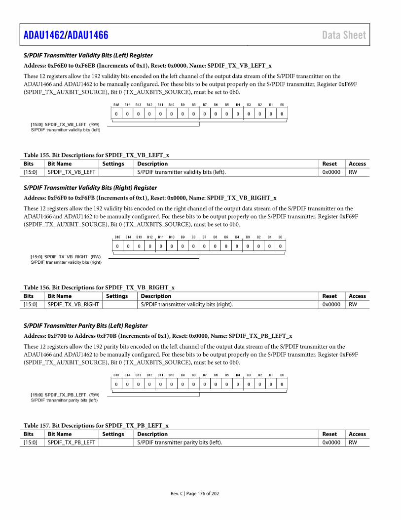
ADAU1462/ADAU1466 Data Sheet
Rev. C | Page 176 of 202
S/PDIF Transmitter Validity Bits (Left) Register
Address: 0xF6E0 to 0xF6EB (Increments of 0x1), Reset: 0x0000, Name: SPDIF_TX_VB_LEFT_x
These 12 registers allow the 192 validity bits encoded on the left channel of the output data stream of the S/PDIF transmitter on the ADAU1466 and ADAU1462 to be manually configured. For these bits to be output properly on the S/PDIF transmitter, Register 0xF69F (SPDIF_TX_AUXBIT_SOURCE), Bit 0 (TX_AUXBITS_SOURCE), must be set to 0b0.
Table 155. Bit Descriptions for SPDIF_TX_VB_LEFT_x Bits Bit Name Settings Description Reset Access [15:0] SPDIF_TX_VB_LEFT S/PDIF transmitter validity bits (left). 0x0000 RW
S/PDIF Transmitter Validity Bits (Right) Register
Address: 0xF6F0 to 0xF6FB (Increments of 0x1), Reset: 0x0000, Name: SPDIF_TX_VB_RIGHT_x
These 12 registers allow the 192 validity bits encoded on the right channel of the output data stream of the S/PDIF transmitter on the ADAU1466 and ADAU1462 to be manually configured. For these bits to be output properly on the S/PDIF transmitter, Register 0xF69F (SPDIF_TX_AUXBIT_SOURCE), Bit 0 (TX_AUXBITS_SOURCE), must be set to 0b0.
Table 156. Bit Descriptions for SPDIF_TX_VB_RIGHT_x Bits Bit Name Settings Description Reset Access [15:0] SPDIF_TX_VB_RIGHT S/PDIF transmitter validity bits (right). 0x0000 RW
S/PDIF Transmitter Parity Bits (Left) Register
Address: 0xF700 to Address 0xF70B (Increments of 0x1), Reset: 0x0000, Name: SPDIF_TX_PB_LEFT_x
These 12 registers allow the 192 parity bits encoded on the left channel of the output data stream of the S/PDIF transmitter on the ADAU1466 and ADAU1462 to be manually configured. For these bits to be output properly on the S/PDIF transmitter, Register 0xF69F (SPDIF_TX_AUXBIT_SOURCE), Bit 0 (TX_AUXBITS_SOURCE), must be set to 0b0.
Table 157. Bit Descriptions for SPDIF_TX_PB_LEFT_x Bits Bit Name Settings Description Reset Access [15:0] SPDIF_TX_PB_LEFT S/PDIF transmitter parity bits (left). 0x0000 RW
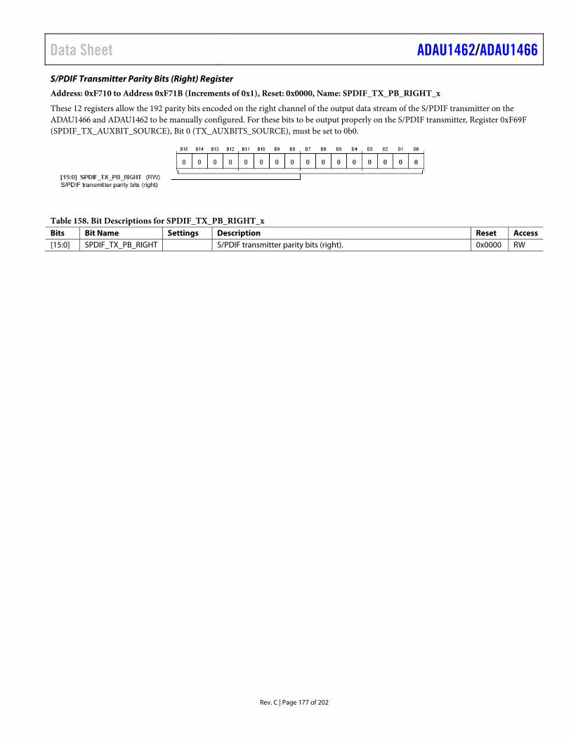
Data Sheet ADAU1462/ADAU1466
Rev. C | Page 177 of 202
S/PDIF Transmitter Parity Bits (Right) Register
Address: 0xF710 to Address 0xF71B (Increments of 0x1), Reset: 0x0000, Name: SPDIF_TX_PB_RIGHT_x
These 12 registers allow the 192 parity bits encoded on the right channel of the output data stream of the S/PDIF transmitter on the ADAU1466 and ADAU1462 to be manually configured. For these bits to be output properly on the S/PDIF transmitter, Register 0xF69F (SPDIF_TX_AUXBIT_SOURCE), Bit 0 (TX_AUXBITS_SOURCE), must be set to 0b0.
Table 158. Bit Descriptions for SPDIF_TX_PB_RIGHT_x Bits Bit Name Settings Description Reset Access [15:0] SPDIF_TX_PB_RIGHT S/PDIF transmitter parity bits (right). 0x0000 RW
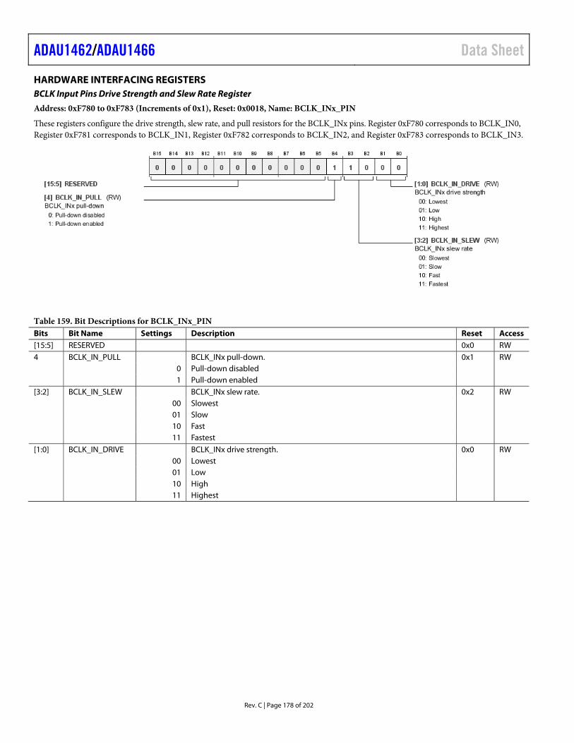
ADAU1462/ADAU1466 Data Sheet
Rev. C | Page 178 of 202
HARDWARE INTERFACING REGISTERS BCLK Input Pins Drive Strength and Slew Rate Register
Address: 0xF780 to 0xF783 (Increments of 0x1), Reset: 0x0018, Name: BCLK_INx_PIN
These registers configure the drive strength, slew rate, and pull resistors for the BCLK_INx pins. Register 0xF780 corresponds to BCLK_IN0, Register 0xF781 corresponds to BCLK_IN1, Register 0xF782 corresponds to BCLK_IN2, and Register 0xF783 corresponds to BCLK_IN3.
Table 159. Bit Descriptions for BCLK_INx_PIN Bits Bit Name Settings Description Reset Access [15:5] RESERVED 0x0 RW 4 BCLK_IN_PULL BCLK_INx pull-down. 0x1 RW 0 Pull-down disabled 1 Pull-down enabled [3:2] BCLK_IN_SLEW BCLK_INx slew rate. 0x2 RW 00 Slowest 01 Slow 10 Fast 11 Fastest [1:0] BCLK_IN_DRIVE BCLK_INx drive strength. 0x0 RW 00 Lowest 01 Low 10 High 11 Highest
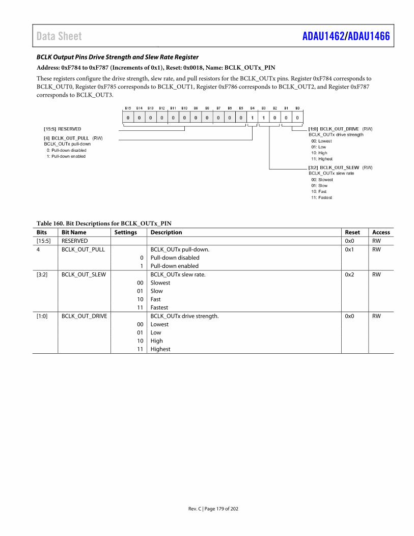
Data Sheet ADAU1462/ADAU1466
Rev. C | Page 179 of 202
BCLK Output Pins Drive Strength and Slew Rate Register
Address: 0xF784 to 0xF787 (Increments of 0x1), Reset: 0x0018, Name: BCLK_OUTx_PIN
These registers configure the drive strength, slew rate, and pull resistors for the BCLK_OUTx pins. Register 0xF784 corresponds to BCLK_OUT0, Register 0xF785 corresponds to BCLK_OUT1, Register 0xF786 corresponds to BCLK_OUT2, and Register 0xF787 corresponds to BCLK_OUT3.
Table 160. Bit Descriptions for BCLK_OUTx_PIN Bits Bit Name Settings Description Reset Access [15:5] RESERVED 0x0 RW 4 BCLK_OUT_PULL BCLK_OUTx pull-down. 0x1 RW 0 Pull-down disabled 1 Pull-down enabled [3:2] BCLK_OUT_SLEW BCLK_OUTx slew rate. 0x2 RW 00 Slowest 01 Slow 10 Fast 11 Fastest [1:0] BCLK_OUT_DRIVE BCLK_OUTx drive strength. 0x0 RW 00 Lowest 01 Low 10 High 11 Highest
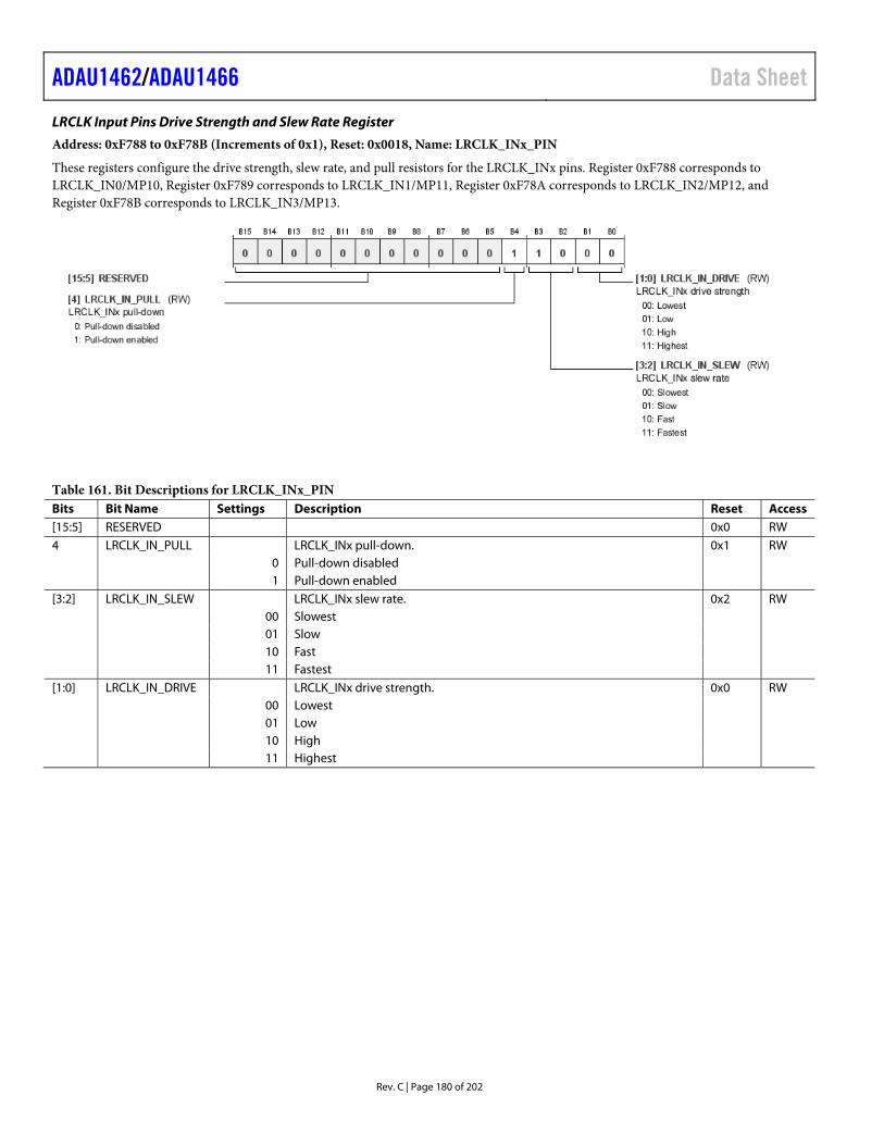
ADAU1462/ADAU1466 Data Sheet
Rev. C | Page 180 of 202
LRCLK Input Pins Drive Strength and Slew Rate Register
Address: 0xF788 to 0xF78B (Increments of 0x1), Reset: 0x0018, Name: LRCLK_INx_PIN
These registers configure the drive strength, slew rate, and pull resistors for the LRCLK_INx pins. Register 0xF788 corresponds to LRCLK_IN0/MP10, Register 0xF789 corresponds to LRCLK_IN1/MP11, Register 0xF78A corresponds to LRCLK_IN2/MP12, and Register 0xF78B corresponds to LRCLK_IN3/MP13.
Table 161. Bit Descriptions for LRCLK_INx_PIN Bits Bit Name Settings Description Reset Access [15:5] RESERVED 0x0 RW 4 LRCLK_IN_PULL LRCLK_INx pull-down. 0x1 RW 0 Pull-down disabled 1 Pull-down enabled [3:2] LRCLK_IN_SLEW LRCLK_INx slew rate. 0x2 RW 00 Slowest 01 Slow 10 Fast 11 Fastest [1:0] LRCLK_IN_DRIVE LRCLK_INx drive strength. 0x0 RW 00 Lowest 01 Low 10 High 11 Highest
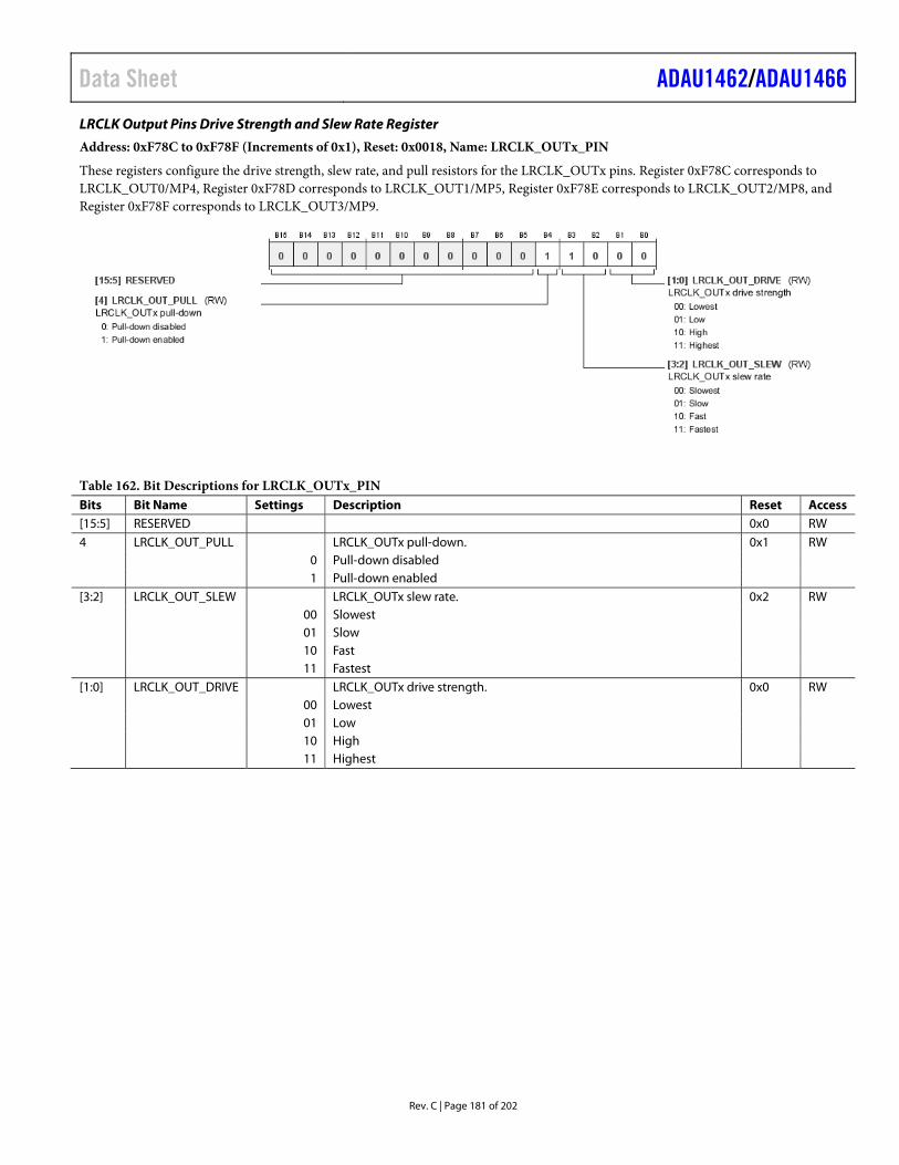
Data Sheet ADAU1462/ADAU1466
Rev. C | Page 181 of 202
LRCLK Output Pins Drive Strength and Slew Rate Register
Address: 0xF78C to 0xF78F (Increments of 0x1), Reset: 0x0018, Name: LRCLK_OUTx_PIN
These registers configure the drive strength, slew rate, and pull resistors for the LRCLK_OUTx pins. Register 0xF78C corresponds to LRCLK_OUT0/MP4, Register 0xF78D corresponds to LRCLK_OUT1/MP5, Register 0xF78E corresponds to LRCLK_OUT2/MP8, and Register 0xF78F corresponds to LRCLK_OUT3/MP9.
Table 162. Bit Descriptions for LRCLK_OUTx_PIN Bits Bit Name Settings Description Reset Access [15:5] RESERVED 0x0 RW 4 LRCLK_OUT_PULL LRCLK_OUTx pull-down. 0x1 RW 0 Pull-down disabled 1 Pull-down enabled [3:2] LRCLK_OUT_SLEW LRCLK_OUTx slew rate. 0x2 RW 00 Slowest 01 Slow 10 Fast 11 Fastest [1:0] LRCLK_OUT_DRIVE LRCLK_OUTx drive strength. 0x0 RW 00 Lowest 01 Low 10 High 11 Highest
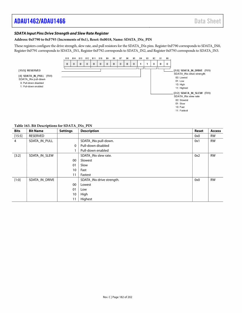
ADAU1462/ADAU1466 Data Sheet
Rev. C | Page 182 of 202
SDATA Input Pins Drive Strength and Slew Rate Register
Address: 0xF790 to 0xF793 (Increments of 0x1), Reset: 0x0018, Name: SDATA_INx_PIN
These registers configure the drive strength, slew rate, and pull resistors for the SDATA_INx pins. Register 0xF790 corresponds to SDATA_IN0, Register 0xF791 corresponds to SDATA_IN1, Register 0xF792 corresponds to SDATA_IN2, and Register 0xF793 corresponds to SDATA_IN3.
Table 163. Bit Descriptions for SDATA_INx_PIN Bits Bit Name Settings Description Reset Access [15:5] RESERVED 0x0 RW 4 SDATA_IN_PULL SDATA_INx pull-down. 0x1 RW 0 Pull-down disabled 1 Pull-down enabled [3:2] SDATA_IN_SLEW SDATA_INx slew rate. 0x2 RW 00 Slowest 01 Slow 10 Fast 11 Fastest [1:0] SDATA_IN_DRIVE SDATA_INx drive strength. 0x0 RW 00 Lowest 01 Low 10 High 11 Highest
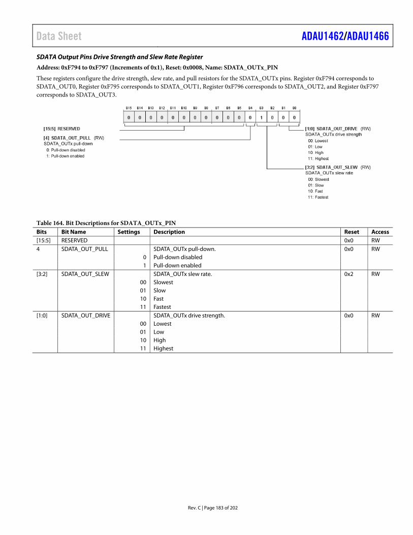
Data Sheet ADAU1462/ADAU1466
Rev. C | Page 183 of 202
SDATA Output Pins Drive Strength and Slew Rate Register
Address: 0xF794 to 0xF797 (Increments of 0x1), Reset: 0x0008, Name: SDATA_OUTx_PIN
These registers configure the drive strength, slew rate, and pull resistors for the SDATA_OUTx pins. Register 0xF794 corresponds to SDATA_OUT0, Register 0xF795 corresponds to SDATA_OUT1, Register 0xF796 corresponds to SDATA_OUT2, and Register 0xF797 corresponds to SDATA_OUT3.
Table 164. Bit Descriptions for SDATA_OUTx_PIN Bits Bit Name Settings Description Reset Access [15:5] RESERVED 0x0 RW 4 SDATA_OUT_PULL SDATA_OUTx pull-down. 0x0 RW 0 Pull-down disabled 1 Pull-down enabled [3:2] SDATA_OUT_SLEW SDATA_OUTx slew rate. 0x2 RW 00 Slowest 01 Slow 10 Fast 11 Fastest [1:0] SDATA_OUT_DRIVE SDATA_OUTx drive strength. 0x0 RW 00 Lowest 01 Low 10 High 11 Highest
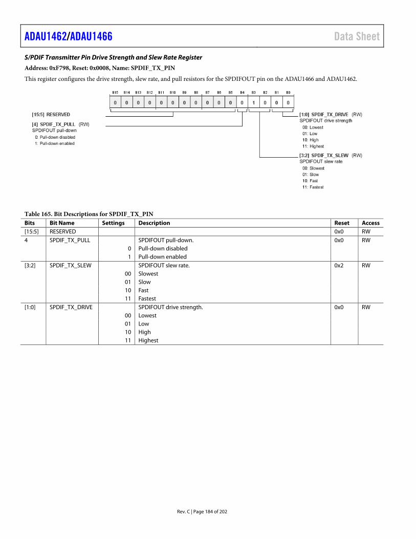
ADAU1462/ADAU1466 Data Sheet
Rev. C | Page 184 of 202
S/PDIF Transmitter Pin Drive Strength and Slew Rate Register
Address: 0xF798, Reset: 0x0008, Name: SPDIF_TX_PIN
This register configures the drive strength, slew rate, and pull resistors for the SPDIFOUT pin on the ADAU1466 and ADAU1462.
Table 165. Bit Descriptions for SPDIF_TX_PIN Bits Bit Name Settings Description Reset Access [15:5] RESERVED 0x0 RW 4 SPDIF_TX_PULL SPDIFOUT pull-down. 0x0 RW 0 Pull-down disabled 1 Pull-down enabled [3:2] SPDIF_TX_SLEW SPDIFOUT slew rate. 0x2 RW 00 Slowest 01 Slow 10 Fast 11 Fastest [1:0] SPDIF_TX_DRIVE SPDIFOUT drive strength. 0x0 RW 00 Lowest 01 Low 10 High 11 Highest

Data Sheet ADAU1462/ADAU1466
Rev. C | Page 185 of 202
SCLK/SCL Pin Drive Strength and Slew Rate Register
Address: 0xF799, Reset: 0x0008, Name: SCLK_SCL_PIN
This register configures the drive strength, slew rate, and pull resistors for the SCLK/SCL pin.
Table 166. Bit Descriptions for SCLK_SCL_PIN Bits Bit Name Settings Description Reset Access [15:5] RESERVED 0x0 RW 4 SCLK_SCL_PULL SCLK/SCL pull-up. 0x0 RW 0 Pull-up disabled 1 Pull-up enabled [3:2] SCLK_SCL_SLEW SCLK/SCL slew rate. 0x2 RW 00 Slowest 01 Slow 10 Fast 11 Fastest [1:0] SCLK_SCL_DRIVE SCLK/SCL drive strength. 0x0 RW 00 Lowest 01 Low 10 High 11 Highest
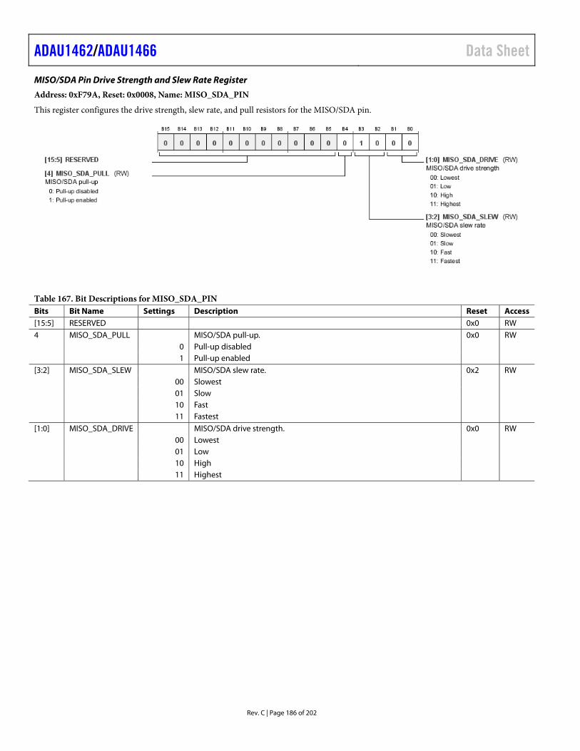
ADAU1462/ADAU1466 Data Sheet
Rev. C | Page 186 of 202
MISO/SDA Pin Drive Strength and Slew Rate Register
Address: 0xF79A, Reset: 0x0008, Name: MISO_SDA_PIN
This register configures the drive strength, slew rate, and pull resistors for the MISO/SDA pin.
Table 167. Bit Descriptions for MISO_SDA_PIN Bits Bit Name Settings Description Reset Access [15:5] RESERVED 0x0 RW 4 MISO_SDA_PULL MISO/SDA pull-up. 0x0 RW 0 Pull-up disabled 1 Pull-up enabled [3:2] MISO_SDA_SLEW MISO/SDA slew rate. 0x2 RW 00 Slowest 01 Slow 10 Fast 11 Fastest [1:0] MISO_SDA_DRIVE MISO/SDA drive strength. 0x0 RW 00 Lowest 01 Low 10 High 11 Highest
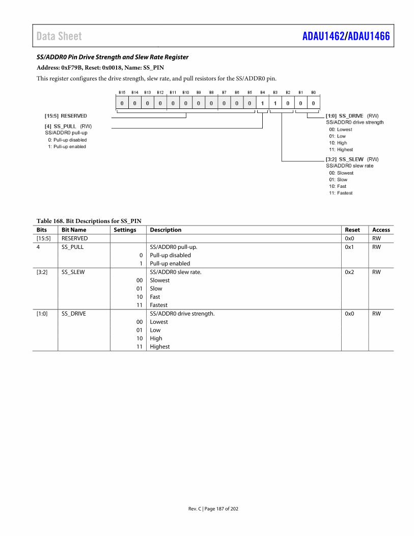
Data Sheet ADAU1462/ADAU1466
Rev. C | Page 187 of 202
SS/ADDR0 Pin Drive Strength and Slew Rate Register
Address: 0xF79B, Reset: 0x0018, Name: SS_PIN
This register configures the drive strength, slew rate, and pull resistors for the SS/ADDR0 pin.
Table 168. Bit Descriptions for SS_PIN Bits Bit Name Settings Description Reset Access [15:5] RESERVED 0x0 RW 4 SS_PULL SS/ADDR0 pull-up. 0x1 RW 0 Pull-up disabled 1 Pull-up enabled [3:2] SS_SLEW SS/ADDR0 slew rate. 0x2 RW 00 Slowest 01 Slow 10 Fast 11 Fastest [1:0] SS_DRIVE SS/ADDR0 drive strength. 0x0 RW 00 Lowest 01 Low 10 High 11 Highest
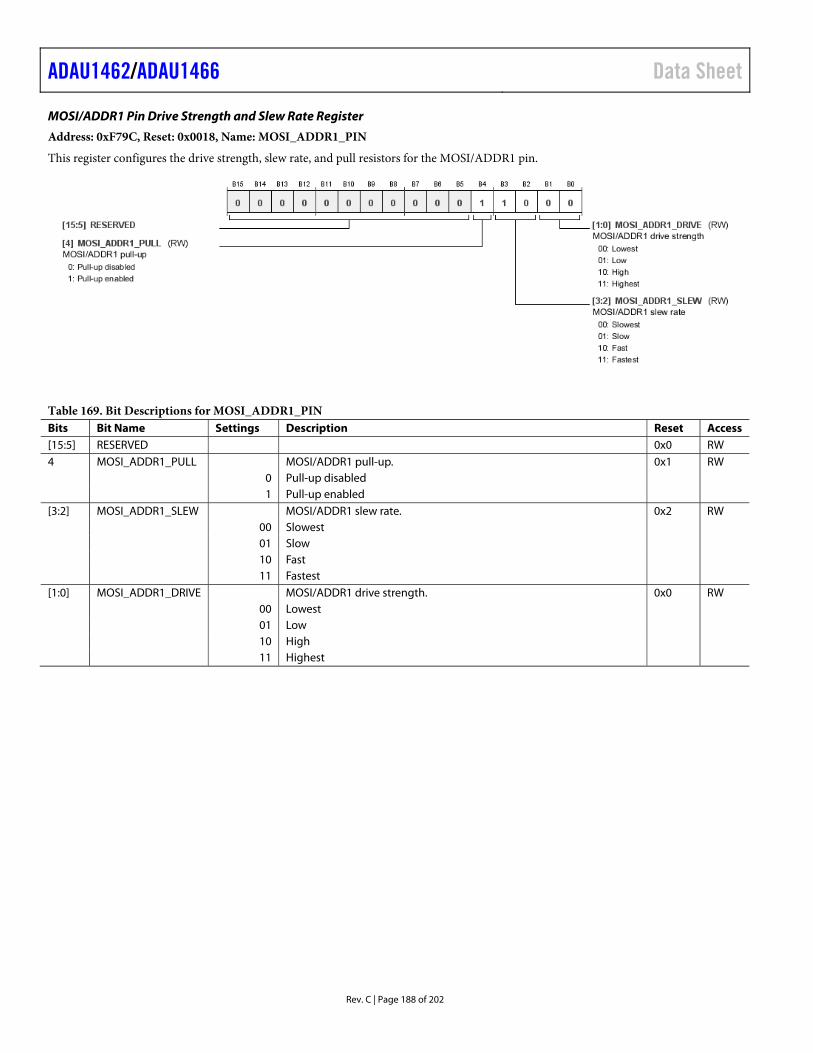
ADAU1462/ADAU1466 Data Sheet
Rev. C | Page 188 of 202
MOSI/ADDR1 Pin Drive Strength and Slew Rate Register
Address: 0xF79C, Reset: 0x0018, Name: MOSI_ADDR1_PIN
This register configures the drive strength, slew rate, and pull resistors for the MOSI/ADDR1 pin.
Table 169. Bit Descriptions for MOSI_ADDR1_PIN Bits Bit Name Settings Description Reset Access [15:5] RESERVED 0x0 RW 4 MOSI_ADDR1_PULL MOSI/ADDR1 pull-up. 0x1 RW 0 Pull-up disabled 1 Pull-up enabled [3:2] MOSI_ADDR1_SLEW MOSI/ADDR1 slew rate. 0x2 RW 00 Slowest 01 Slow 10 Fast 11 Fastest [1:0] MOSI_ADDR1_DRIVE MOSI/ADDR1 drive strength. 0x0 RW 00 Lowest 01 Low 10 High 11 Highest
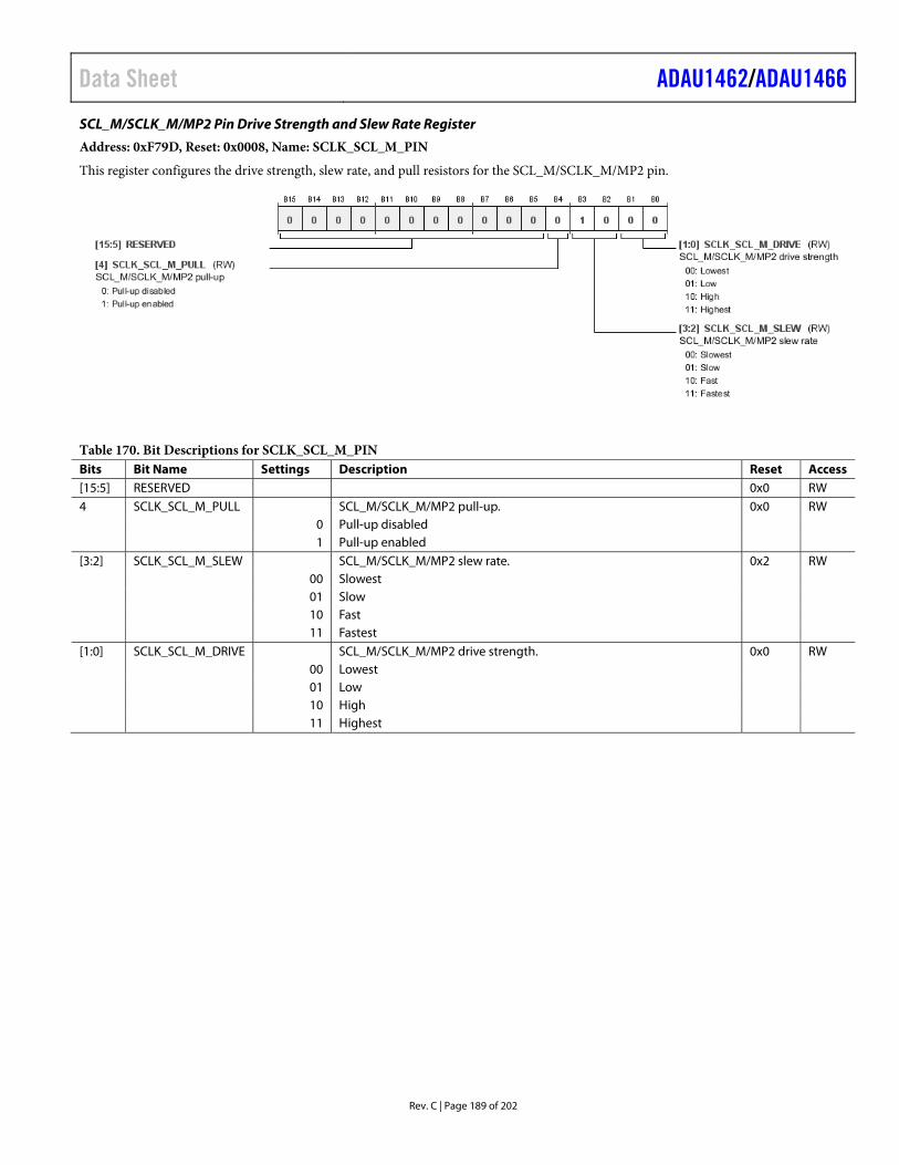
Data Sheet ADAU1462/ADAU1466
Rev. C | Page 189 of 202
SCL_M/SCLK_M/MP2 Pin Drive Strength and Slew Rate Register
Address: 0xF79D, Reset: 0x0008, Name: SCLK_SCL_M_PIN
This register configures the drive strength, slew rate, and pull resistors for the SCL_M/SCLK_M/MP2 pin.
Table 170. Bit Descriptions for SCLK_SCL_M_PIN Bits Bit Name Settings Description Reset Access [15:5] RESERVED 0x0 RW 4 SCLK_SCL_M_PULL SCL_M/SCLK_M/MP2 pull-up. 0x0 RW 0 Pull-up disabled 1 Pull-up enabled [3:2] SCLK_SCL_M_SLEW SCL_M/SCLK_M/MP2 slew rate. 0x2 RW 00 Slowest 01 Slow 10 Fast 11 Fastest [1:0] SCLK_SCL_M_DRIVE SCL_M/SCLK_M/MP2 drive strength. 0x0 RW 00 Lowest 01 Low 10 High 11 Highest
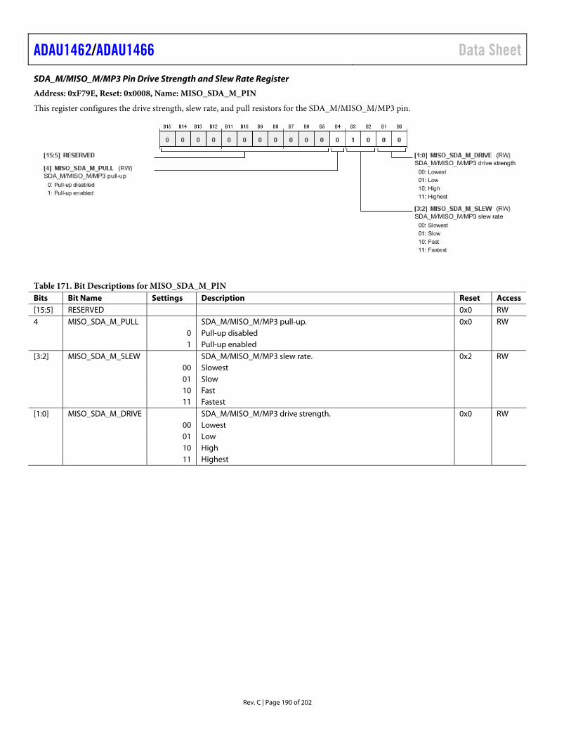
ADAU1462/ADAU1466 Data Sheet
Rev. C | Page 190 of 202
SDA_M/MISO_M/MP3 Pin Drive Strength and Slew Rate Register
Address: 0xF79E, Reset: 0x0008, Name: MISO_SDA_M_PIN
This register configures the drive strength, slew rate, and pull resistors for the SDA_M/MISO_M/MP3 pin.
Table 171. Bit Descriptions for MISO_SDA_M_PIN Bits Bit Name Settings Description Reset Access [15:5] RESERVED 0x0 RW 4 MISO_SDA_M_PULL SDA_M/MISO_M/MP3 pull-up. 0x0 RW 0 Pull-up disabled 1 Pull-up enabled [3:2] MISO_SDA_M_SLEW SDA_M/MISO_M/MP3 slew rate. 0x2 RW 00 Slowest 01 Slow 10 Fast 11 Fastest [1:0] MISO_SDA_M_DRIVE SDA_M/MISO_M/MP3 drive strength. 0x0 RW 00 Lowest 01 Low 10 High 11 Highest
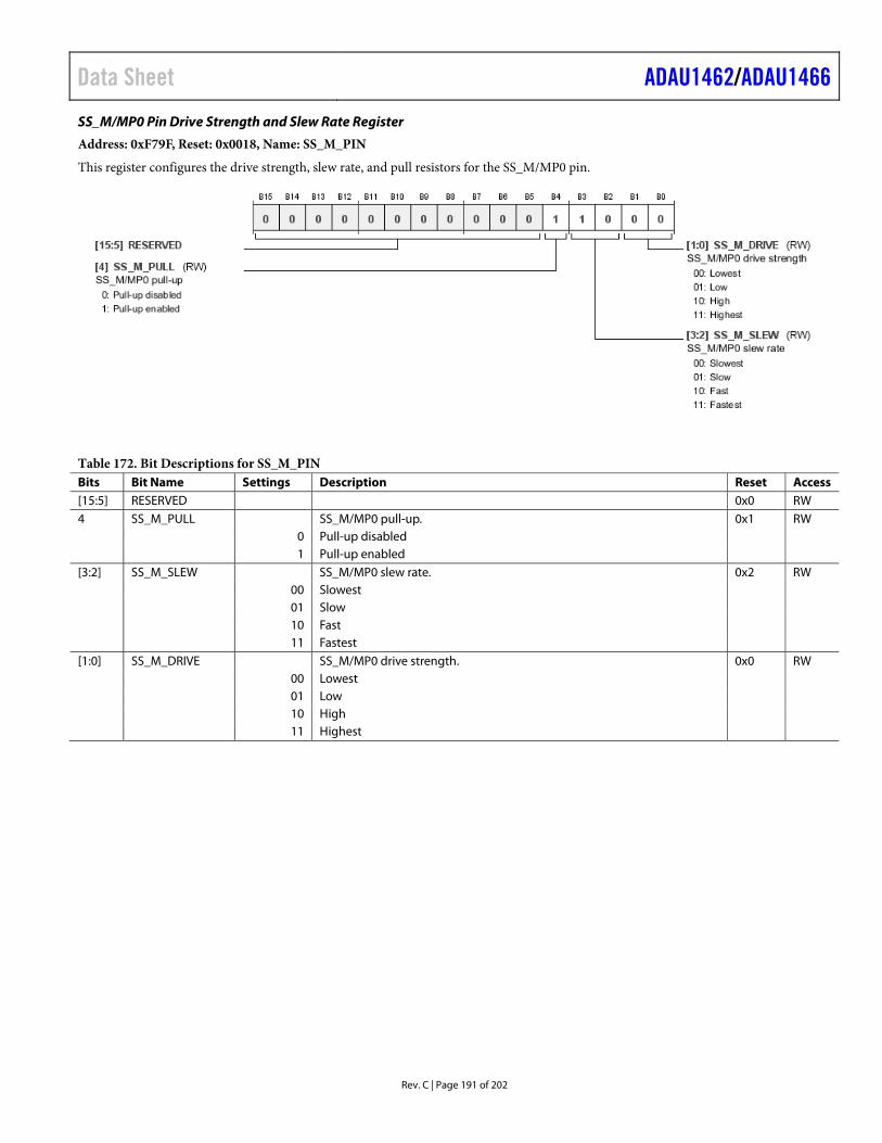
Data Sheet ADAU1462/ADAU1466
Rev. C | Page 191 of 202
SS_M/MP0 Pin Drive Strength and Slew Rate Register
Address: 0xF79F, Reset: 0x0018, Name: SS_M_PIN
This register configures the drive strength, slew rate, and pull resistors for the SS_M/MP0 pin.
Table 172. Bit Descriptions for SS_M_PIN Bits Bit Name Settings Description Reset Access [15:5] RESERVED 0x0 RW 4 SS_M_PULL SS_M/MP0 pull-up. 0x1 RW 0 Pull-up disabled 1 Pull-up enabled [3:2] SS_M_SLEW SS_M/MP0 slew rate. 0x2 RW 00 Slowest 01 Slow 10 Fast 11 Fastest [1:0] SS_M_DRIVE SS_M/MP0 drive strength. 0x0 RW 00 Lowest 01 Low 10 High 11 Highest
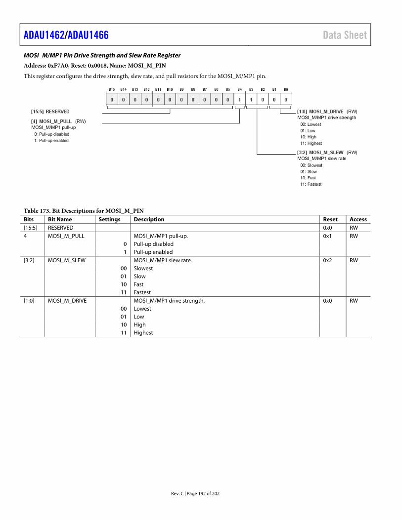
ADAU1462/ADAU1466 Data Sheet
Rev. C | Page 192 of 202
MOSI_M/MP1 Pin Drive Strength and Slew Rate Register
Address: 0xF7A0, Reset: 0x0018, Name: MOSI_M_PIN
This register configures the drive strength, slew rate, and pull resistors for the MOSI_M/MP1 pin.
Table 173. Bit Descriptions for MOSI_M_PIN Bits Bit Name Settings Description Reset Access [15:5] RESERVED 0x0 RW 4 MOSI_M_PULL MOSI_M/MP1 pull-up. 0x1 RW 0 Pull-up disabled 1 Pull-up enabled [3:2] MOSI_M_SLEW MOSI_M/MP1 slew rate. 0x2 RW 00 Slowest 01 Slow 10 Fast 11 Fastest [1:0] MOSI_M_DRIVE MOSI_M/MP1 drive strength. 0x0 RW 00 Lowest 01 Low 10 High 11 Highest

Data Sheet ADAU1462/ADAU1466
Rev. C | Page 193 of 202
MP6 Pin Drive Strength and Slew Rate Register
Address: 0xF7A1, Reset: 0x0018, Name: MP6_PIN
This register configures the drive strength, slew rate, and pull resistors for the MP6 pin.
Table 174. Bit Descriptions for MP6_PIN Bits Bit Name Settings Description Reset Access [15:5] RESERVED 0x0 RW 4 MP6_PULL MP6 pull-down. 0x1 RW 0 Pull-down disabled 1 Pull-down enabled [3:2] MP6_SLEW MP6 slew rate. 0x2 RW 00 Slowest 01 Slow 10 Fast 11 Fastest [1:0] MP6_DRIVE MP6 drive strength. 0x0 RW 00 Lowest 01 Low 10 High 11 Highest
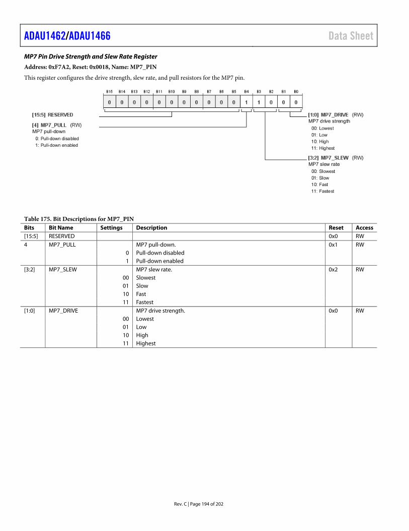
ADAU1462/ADAU1466 Data Sheet
Rev. C | Page 194 of 202
MP7 Pin Drive Strength and Slew Rate Register
Address: 0xF7A2, Reset: 0x0018, Name: MP7_PIN
This register configures the drive strength, slew rate, and pull resistors for the MP7 pin.
Table 175. Bit Descriptions for MP7_PIN Bits Bit Name Settings Description Reset Access [15:5] RESERVED 0x0 RW 4 MP7_PULL MP7 pull-down. 0x1 RW 0 Pull-down disabled 1 Pull-down enabled [3:2] MP7_SLEW MP7 slew rate. 0x2 RW 00 Slowest 01 Slow 10 Fast 11 Fastest [1:0] MP7_DRIVE MP7 drive strength. 0x0 RW 00 Lowest 01 Low 10 High 11 Highest
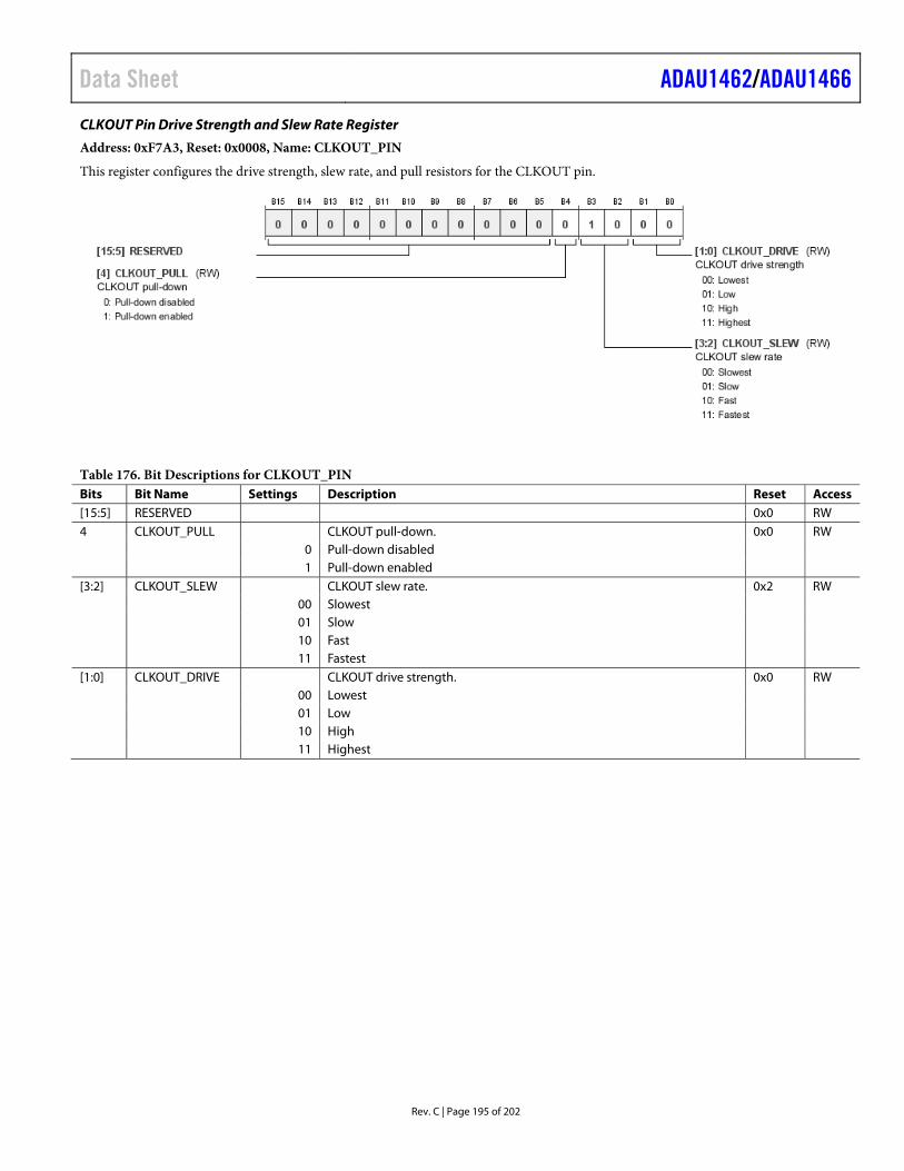
Data Sheet ADAU1462/ADAU1466
Rev. C | Page 195 of 202
CLKOUT Pin Drive Strength and Slew Rate Register
Address: 0xF7A3, Reset: 0x0008, Name: CLKOUT_PIN
This register configures the drive strength, slew rate, and pull resistors for the CLKOUT pin.
Table 176. Bit Descriptions for CLKOUT_PIN Bits Bit Name Settings Description Reset Access [15:5] RESERVED 0x0 RW 4 CLKOUT_PULL CLKOUT pull-down. 0x0 RW 0 Pull-down disabled 1 Pull-down enabled [3:2] CLKOUT_SLEW CLKOUT slew rate. 0x2 RW 00 Slowest 01 Slow 10 Fast 11 Fastest [1:0] CLKOUT_DRIVE CLKOUT drive strength. 0x0 RW 00 Lowest 01 Low 10 High 11 Highest
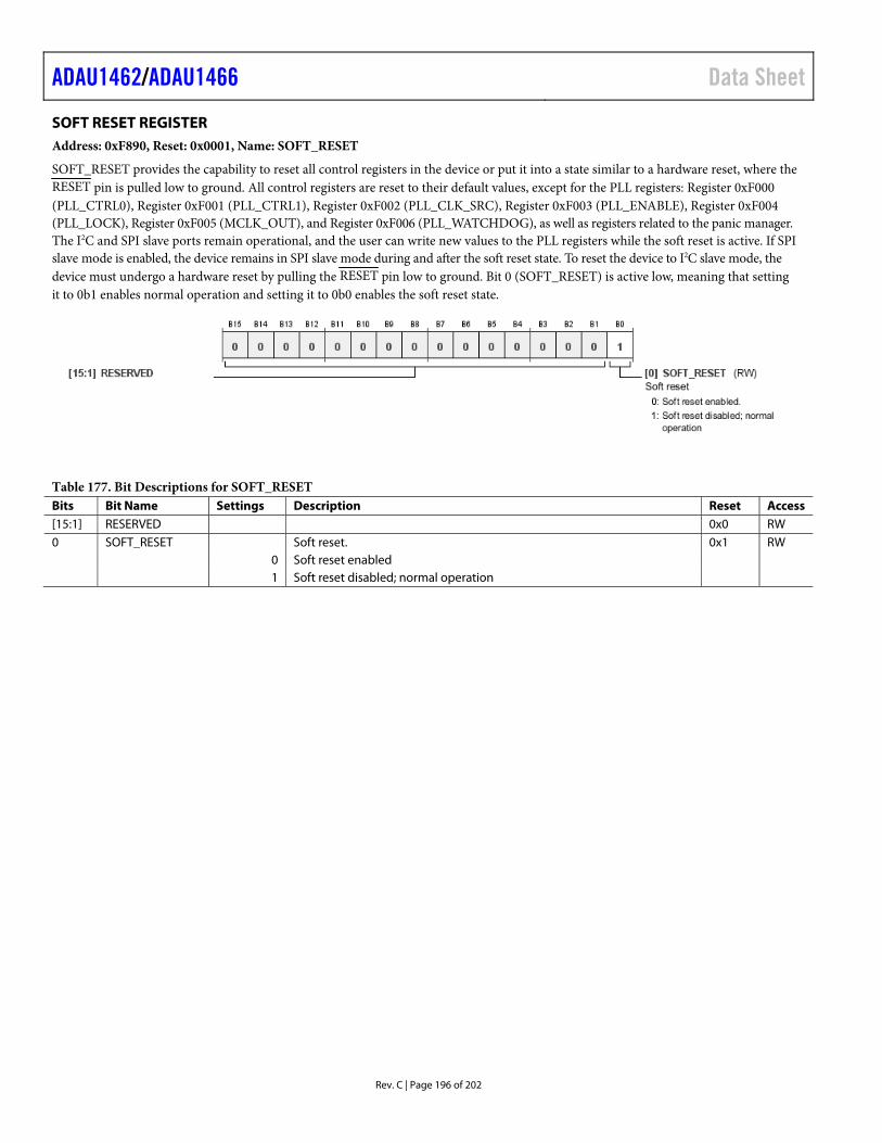
ADAU1462/ADAU1466 Data Sheet
Rev. C | Page 196 of 202
SOFT RESET REGISTER Address: 0xF890, Reset: 0x0001, Name: SOFT_RESET
SOFT_RESET provides the capability to reset all control registers in the device or put it into a state similar to a hardware reset, where the RESET pin is pulled low to ground. All control registers are reset to their default values, except for the PLL registers: Register 0xF000 (PLL_CTRL0), Register 0xF001 (PLL_CTRL1), Register 0xF002 (PLL_CLK_SRC), Register 0xF003 (PLL_ENABLE), Register 0xF004 (PLL_LOCK), Register 0xF005 (MCLK_OUT), and Register 0xF006 (PLL_WATCHDOG), as well as registers related to the panic manager. The I2C and SPI slave ports remain operational, and the user can write new values to the PLL registers while the soft reset is active. If SPI slave mode is enabled, the device remains in SPI slave mode during and after the soft reset state. To reset the device to I2C slave mode, the device must undergo a hardware reset by pulling the RESET pin low to ground. Bit 0 (SOFT_RESET) is active low, meaning that setting it to 0b1 enables normal operation and setting it to 0b0 enables the soft reset state.
Table 177. Bit Descriptions for SOFT_RESET Bits Bit Name Settings Description Reset Access [15:1] RESERVED 0x0 RW 0 SOFT_RESET Soft reset. 0x1 RW 0 Soft reset enabled 1 Soft reset disabled; normal operation
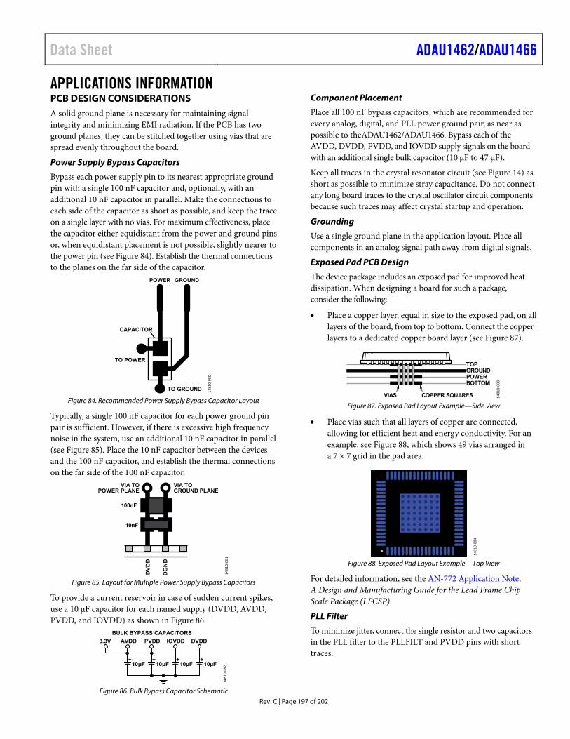
Data Sheet ADAU1462/ADAU1466
Rev. C | Page 197 of 202
APPLICATIONS INFORMATION PCB DESIGN CONSIDERATIONS A solid ground plane is necessary for maintaining signal integrity and minimizing EMI radiation. If the PCB has two ground planes, they can be stitched together using vias that are spread evenly throughout the board.
Power Supply Bypass Capacitors
Bypass each power supply pin to its nearest appropriate ground pin with a single 100 nF capacitor and, optionally, with an additional 10 nF capacitor in parallel. Make the connections to each side of the capacitor as short as possible, and keep the trace on a single layer with no vias. For maximum effectiveness, place the capacitor either equidistant from the power and ground pins or, when equidistant placement is not possible, slightly nearer to the power pin (see Figure 84). Establish the thermal connections to the planes on the far side of the capacitor.
POWER GROUND
TO GROUND
TO POWER
CAPACITOR
14
81
0-0
80
Figure 84. Recommended Power Supply Bypass Capacitor Layout
Typically, a single 100 nF capacitor for each power ground pin pair is sufficient. However, if there is excessive high frequency noise in the system, use an additional 10 nF capacitor in parallel (see Figure 85). Place the 10 nF capacitor between the devices and the 100 nF capacitor, and establish the thermal connections on the far side of the 100 nF capacitor.
VIA TOPOWER PLANE
DV
DD
DG
ND
VIA TOGROUND PLANE
10nF
100nF
14
81
0-0
81
Figure 85. Layout for Multiple Power Supply Bypass Capacitors
To provide a current reservoir in case of sudden current spikes, use a 10 μF capacitor for each named supply (DVDD, AVDD, PVDD, and IOVDD) as shown in Figure 86.
BULK BYPASS CAPACITORS
3.3V AVDD PVDD IOVDD DVDD
10µF+
10µF+
10µF+
10µF+
1481
0-0
82
Figure 86. Bulk Bypass Capacitor Schematic
Component Placement
Place all 100 nF bypass capacitors, which are recommended for every analog, digital, and PLL power ground pair, as near as possible to theADAU1462/ADAU1466. Bypass each of the AVDD, DVDD, PVDD, and IOVDD supply signals on the board with an additional single bulk capacitor (10 μF to 47 μF).
Keep all traces in the crystal resonator circuit (see Figure 14) as short as possible to minimize stray capacitance. Do not connect any long board traces to the crystal oscillator circuit components because such traces may affect crystal startup and operation.
Grounding
Use a single ground plane in the application layout. Place all components in an analog signal path away from digital signals.
Exposed Pad PCB Design
The device package includes an exposed pad for improved heat dissipation. When designing a board for such a package, consider the following:
Place a copper layer, equal in size to the exposed pad, on all layers of the board, from top to bottom. Connect the copper layers to a dedicated copper board layer (see Figure 87).
14
81
0-0
83
Figure 87. Exposed Pad Layout Example—Side View
Place vias such that all layers of copper are connected, allowing for efficient heat and energy conductivity. For an example, see Figure 88, which shows 49 vias arranged in a 7 × 7 grid in the pad area.
1481
0-08
4
Figure 88. Exposed Pad Layout Example—Top View
For detailed information, see the AN-772 Application Note, A Design and Manufacturing Guide for the Lead Frame Chip Scale Package (LFCSP).
PLL Filter
To minimize jitter, connect the single resistor and two capacitors in the PLL filter to the PLLFILT and PVDD pins with short traces.
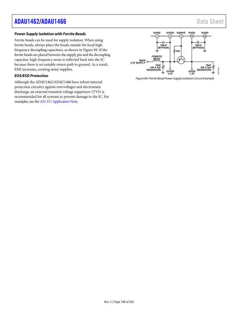
ADAU1462/ADAU1466 Data Sheet
Rev. C | Page 198 of 202
Power Supply Isolation with Ferrite Beads
Ferrite beads can be used for supply isolation. When using ferrite beads, always place the beads outside the local high frequency decoupling capacitors, as shown in Figure 89. If the ferrite beads are placed between the supply pin and the decoupling capacitor, high frequency noise is reflected back into the IC because there is no suitable return path to ground. As a result, EMI increases, creating noisy supplies.
EOS/ESD Protection
Although the ADAU1462/ADAU1466 have robust internal protection circuitry against overvoltages and electrostatic discharge, an external transient voltage suppressor (TVS) is recommended for all systems to prevent damage to the IC. For examples, see the AN-311 Application Note.
DGND IOVDD
IOVDD3.3V
DVDD1.2V
VDRIVE
100nF(BYPASS)
100nF(BYPASS)
1kΩ
DVDD
10µFOR 4.7µF
RESERVOIR
MAIN3.3V SUPPLY
FERRITEBEAD
+10µFOR 4.7µF
RESERVOIR
+
DGND1 32 71 72
1481
0-08
5
Figure 89. Ferrite Bead Power Supply Isolation Circuit Example
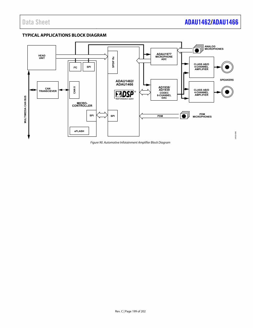
Data Sheet ADAU1462/ADAU1466
Rev. C | Page 199 of 202
TYPICAL APPLICATIONS BLOCK DIAGRAM
SPI
SPI SP
DIF
Rx
CANTRANSCIEVER
HEADUNIT
I2C
CA
N 0
SPI PDMPDM
MICROPHONES
CLASS AB/D4-CHANNELAMPLIFIER
CLASS AB/D4-CHANNELAMPLIFIER
SPEAKERS
ANALOGMICROPHONES
ADAU1977MICROPHONE
ADC
AD1938/AD1939CODEC
8-CHANNELDAC
eFLASH
MICRO-CONTROLLER
MU
LT
IME
DIA
CA
N B
US
148
10-0
86
ADAU1462/ADAU1466
®
Figure 90. Automotive Infotainment Amplifier Block Diagram
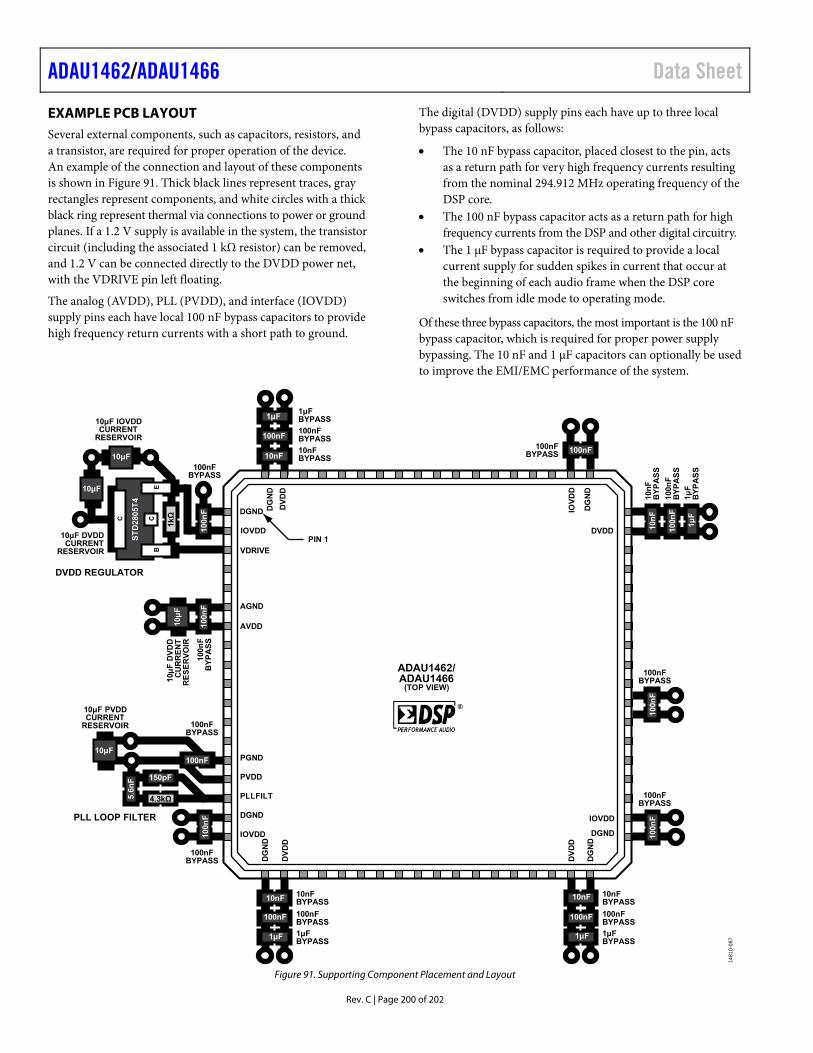
ADAU1462/ADAU1466 Data Sheet
Rev. C | Page 200 of 202
EXAMPLE PCB LAYOUT Several external components, such as capacitors, resistors, and a transistor, are required for proper operation of the device. An example of the connection and layout of these components is shown in Figure 91. Thick black lines represent traces, gray rectangles represent components, and white circles with a thick black ring represent thermal via connections to power or ground planes. If a 1.2 V supply is available in the system, the transistor circuit (including the associated 1 kΩ resistor) can be removed, and 1.2 V can be connected directly to the DVDD power net, with the VDRIVE pin left floating.
The analog (AVDD), PLL (PVDD), and interface (IOVDD) supply pins each have local 100 nF bypass capacitors to provide high frequency return currents with a short path to ground.
The digital (DVDD) supply pins each have up to three local bypass capacitors, as follows:
The 10 nF bypass capacitor, placed closest to the pin, acts as a return path for very high frequency currents resulting from the nominal 294.912 MHz operating frequency of the DSP core.
The 100 nF bypass capacitor acts as a return path for high frequency currents from the DSP and other digital circuitry.
The 1 μF bypass capacitor is required to provide a local current supply for sudden spikes in current that occur at the beginning of each audio frame when the DSP core switches from idle mode to operating mode.
Of these three bypass capacitors, the most important is the 100 nF bypass capacitor, which is required for proper power supply bypassing. The 10 nF and 1 μF capacitors can optionally be used to improve the EMI/EMC performance of the system.
1μFBYPASS
1μF
BY
PA
SS
10μF DVDDCURRENT
RESERVOIR
10μ
F D
VD
DC
UR
RE
NT
RE
SE
RV
OIR
10μF IOVDDCURRENT
RESERVOIR
10μF PVDDCURRENT
RESERVOIR
PLL LOOP FILTER
DVDD REGULATOR
IOVDD
IOVDDDGND
PLLFILT
PVDD
PGND
AVDD
AGND
DG
ND
DG
ND
DGND
DV
DD
DV
DD
VDRIVE
IOVDD
C CE
B
ST
D28
05T
4
100nFBYPASS
100nFBYPASS
100n
FB
YP
AS
S
100nFBYPASS
100nFBYPASS
10nFBYPASS
10n
FB
YP
AS
S
100nFBYPASS
100nFBYPASS
100nFBYPASS
100n
FB
YP
AS
S
PIN 1
10nF
100nF
100n
F
100nF
100n
F
100n
F
1μF
10n
F
100n
F
100n
F
100n
F
100nF
1μF
10μ
F
10μF
10μF
IOV
DD
DG
ND
DG
ND
DGND
DVDD
DV
DD
1μFBYPASS
10nFBYPASS
100nFBYPASS
10nF
100nF
1μF1μFBYPASS
10nFBYPASS
100nFBYPASS
10nF
100nF
1μF
10μF
1kΩ
150pF
4.3kΩ5.6n
F
ADAU1462/ADAU1466
(TOP VIEW)
148
10-0
87
®
Figure 91. Supporting Component Placement and Layout
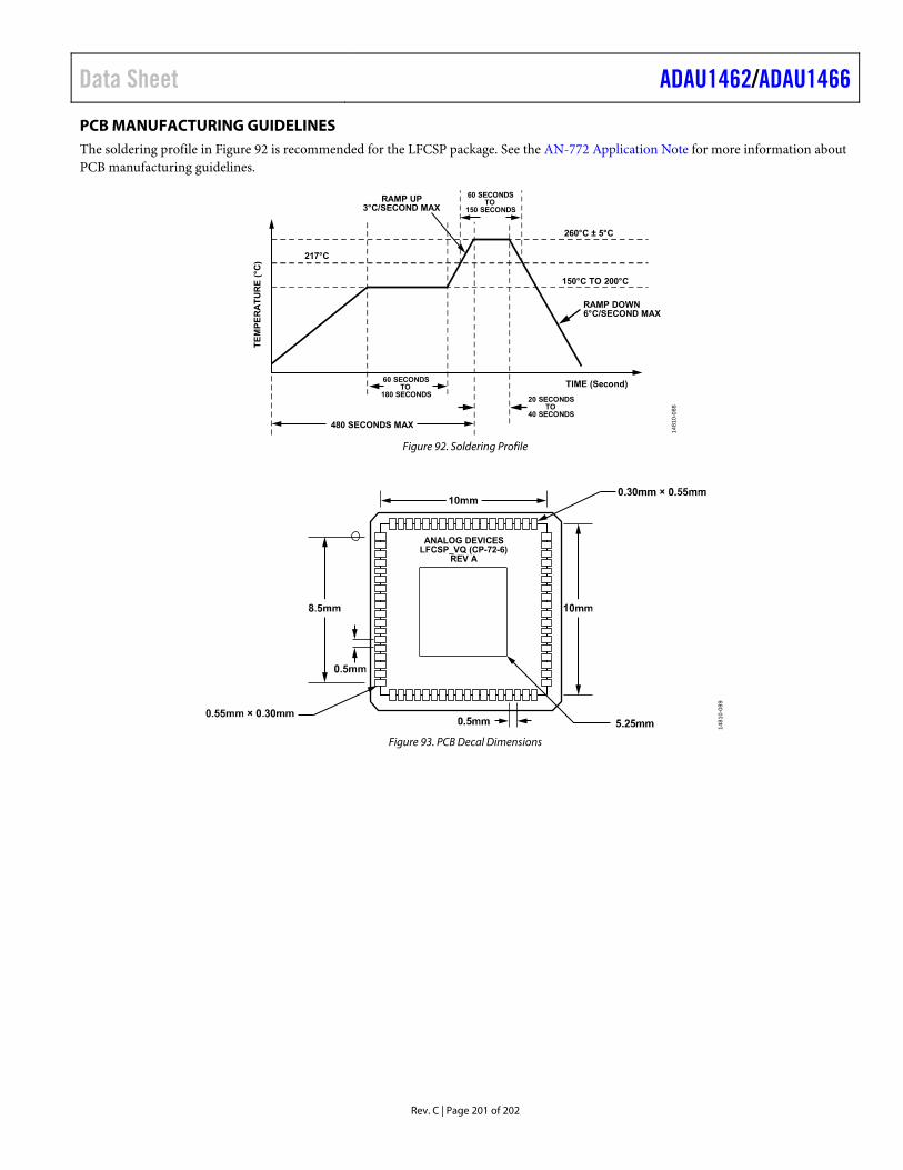
Data Sheet ADAU1462/ADAU1466
Rev. C | Page 201 of 202
PCB MANUFACTURING GUIDELINES The soldering profile in Figure 92 is recommended for the LFCSP package. See the AN-772 Application Note for more information about PCB manufacturing guidelines.
TE
MP
ER
AT
UR
E (
°C)
TIME (Second)
RAMP DOWN6°C/SECOND MAX
217°C
150°C TO 200°C
260°C ± 5°C
RAMP UP3°C/SECOND MAX
60 SECONDSTO
150 SECONDS
60 SECONDSTO
180 SECONDS20 SECONDS
TO40 SECONDS
480 SECONDS MAX
14
810
-08
8
Figure 92. Soldering Profile
ANALOG DEVICESLFCSP_VQ (CP-72-6)
REV A
14
810
-089
Figure 93. PCB Decal Dimensions
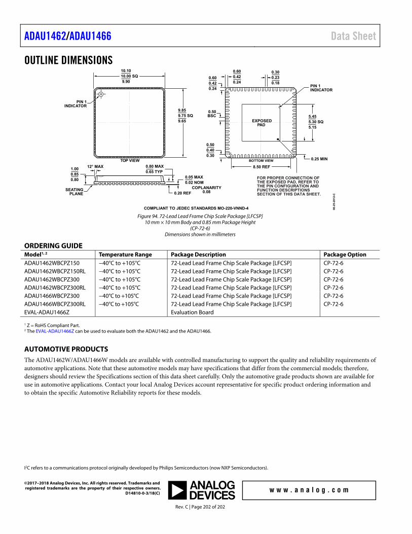
ADAU1462/ADAU1466 Data Sheet
Rev. C | Page 202 of 202
OUTLINE DIMENSIONS
COMPLIANT TO JEDEC STANDARDS MO-220-VNND-4
0.20 REF
0.80 MAX0.65 TYP
1.000.850.80
0.05 MAX0.02 NOM
1
18
54
37
1936
7255
0.500.400.30
8.50 REF
PIN 1INDICATOR
SEATINGPLANE
12° MAX
0.600.420.24
0.600.420.24
0.300.230.18
0.50BSC
PIN 1INDICATOR
COPLANARITY0.08
06-2
5-2
012
-C
FOR PROPER CONNECTION OFTHE EXPOSED PAD, REFER TOTHE PIN CONFIGURATION ANDFUNCTION DESCRIPTIONSSECTION OF THIS DATA SHEET.
TOP VIEW
EXPOSEDPAD
BOTTOM VIEW
10.1010.00 SQ9.90
9.859.75 SQ9.65
0.25 MIN
5.455.30 SQ5.15
Figure 94. 72-Lead Lead Frame Chip Scale Package [LFCSP] 10 mm × 10 mm Body and 0.85 mm Package Height
(CP-72-6) Dimensions shown in millimeters
ORDERING GUIDE Model1, 2 Temperature Range Package Description Package Option ADAU1462WBCPZ150 −40°C to +105°C 72-Lead Lead Frame Chip Scale Package [LFCSP] CP-72-6 ADAU1462WBCPZ150RL −40°C to +105°C 72-Lead Lead Frame Chip Scale Package [LFCSP] CP-72-6 ADAU1462WBCPZ300 −40°C to +105°C 72-Lead Lead Frame Chip Scale Package [LFCSP] CP-72-6 ADAU1462WBCPZ300RL −40°C to +105°C 72-Lead Lead Frame Chip Scale Package [LFCSP] CP-72-6 ADAU1466WBCPZ300 −40°C to +105°C 72-Lead Lead Frame Chip Scale Package [LFCSP] CP-72-6 ADAU1466WBCPZ300RL −40°C to +105°C 72-Lead Lead Frame Chip Scale Package [LFCSP] CP-72-6 EVAL-ADAU1466Z Evaluation Board
1 Z = RoHS Compliant Part. 2 The EVAL-ADAU1466Z can be used to evaluate both the ADAU1462 and the ADAU1466.
AUTOMOTIVE PRODUCTS The ADAU1462W/ADAU1466W models are available with controlled manufacturing to support the quality and reliability requirements of automotive applications. Note that these automotive models may have specifications that differ from the commercial models; therefore, designers should review the Specifications section of this data sheet carefully. Only the automotive grade products shown are available for use in automotive applications. Contact your local Analog Devices account representative for specific product ordering information and to obtain the specific Automotive Reliability reports for these models.
I2C refers to a communications protocol originally developed by Philips Semiconductors (now NXP Semiconductors).
©2017–2018 Analog Devices, Inc. All rights reserved. Trademarks and registered trademarks are the property of their respective owners.
D14810-0-3/18(C)