SiGe Heterojunction Bipolar Technology and Applications · SiGe Heterojunction Bipolar Technology...
41
SiGe Heterojunction Bipolar Technology and Applications J. Prasad Maxim Integrated Products [email protected] 2/17/05
Transcript of SiGe Heterojunction Bipolar Technology and Applications · SiGe Heterojunction Bipolar Technology...

SiGe Heterojunction Bipolar Technologyand Applications
J. PrasadMaxim Integrated Products
[email protected]/17/05
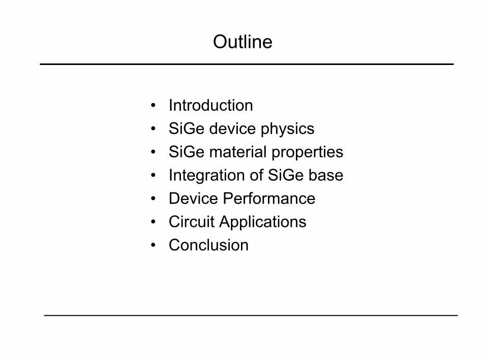
Outline
• Introduction• SiGe device physics• SiGe material properties• Integration of SiGe base• Device Performance• Circuit Applications• Conclusion

Device Physics behind the SiGe HBT
NDE , WE NDE > NAB for a Si bipolarNAB , WB NDC , WC
Si SiGe Si
Base CollectorEmitterβSi
βSiGe = NDE WE Dnb We can trade current gain β and increase base doping NAB
exp (∆Eg / kT) NAB WB Dpe We can decrease emitter doping NDE to get lower Cje ( NDE < NAB )
q NAB WB2
VA = Early Voltage is increased with base doping NABεoεs
fTfmax = fmax improved by lower Rb due to increased NAB8πRbCjc
BVCBO n = 4 for NPNBVCEO =
βn
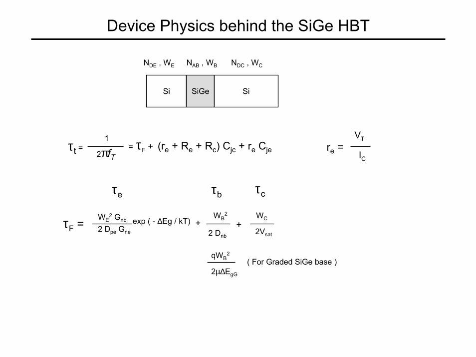
Device Physics behind the SiGe HBT
NDE , WE NAB , WB NDC , WC
Si SiGe Si
VT1= τF + (re + Re + Rc) Cjc + re Cjeτt = re =
2πfT IC
τcτe τb
τF = WE2 Gnb
2 Dpe Gne
exp ( - ∆Eg / kT) +2 Dnb
+WB
2 WC
2Vsat
qWB2
( For Graded SiGe base )2µ∆EgG

Results from Box base SiGe Transistor
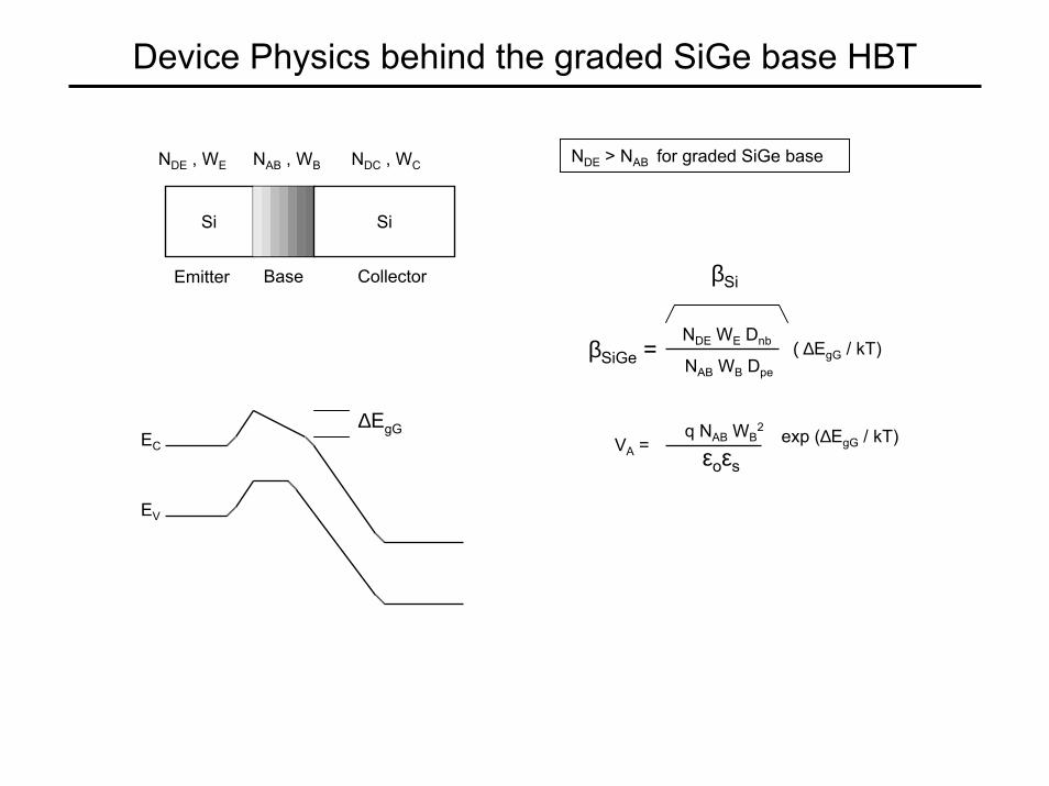
Device Physics behind the graded SiGe base HBT
NDE > NAB for graded SiGe baseNDE , WE NAB , WB NDC , WC
Si Si
βSiBase CollectorEmitter
βSiGe = NDE WE Dnb ( ∆EgG / kT) NAB WB Dpe
∆EgG q NAB WB2 exp (∆EgG / kT) EC VA = εoεs
EV

I-V Curves for a typical SiGe Transistor
0.00E+00
2.00E-04
4.00E-04
6.00E-04
8.00E-04
1.00E-03
1.20E-03
1.40E-03
1.60E-03
1.80E-03
2.00E-03
0.0 0.5 1.0 1.5 2.0 2.5 3.0 3.5
VCE
IC
IB = 0.000e+000IB = 4.000e-006IB = 8.000e-006IB = 1.200e-005IB = 1.600e-005IB = 2.000e-005
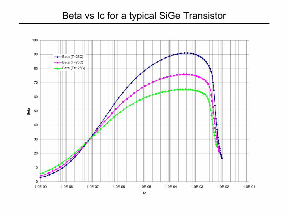
Beta vs Ic for a typical SiGe Transistor
0
10
20
30
40
50
60
70
80
90
100
1.0E-09 1.0E-08 1.0E-07 1.0E-06 1.0E-05 1.0E-04 1.0E-03 1.0E-02 1.0E-01
Ic
Beta
Beta (T=25C)Beta (T=75C)Beta (T=125C)

Device Physics behind the graded SiGe base HBT
NDE , WE NAB , WB NDC , WC
NDE > NAB for graded SiGe baseSi Si
Base CollectorEmitter
VT1= τF + (re + Re + Rc) Cjc + re Cjeτt = re =
2πfT IC
τF = τe + τb + τc
τe (SiGe) Rbi (Si) kT=τe (Si) Rbi (SiGe) ∆EgG
τb (SiGe)
τb (Si)= 2kT )kT( 1 -
∆EgG∆EgG

Results from Triangular base SiGe Transistor

Comparing Box and Triangular Profiles
Box Ge Profile Triangular Ge Profile
• Double Heterojunction - difficult to grow
• beta ~ exp (∆Eg /kT)• VA improved only by base doping• Low base resistance• No significant improvement in fT• Significant improvement in fmax• NDE < NAB
• High Ge content, Lo thermal budget
• Lightly doped emitter has to be grown
• Integration difficult due to grown emitter
• Single Heterojunction - simpler growth
• beta ~ (∆EgG/kT)• VA improved by exp (∆EgG/kT)• High base resistance• fT improved by base transit time• fmax improved thru fT• NDE > NAB
• Lo Ge content, more tolerant • Emitter need not be grown• Easily integrates in a poly emitter
process

Collector Design: Effect of Collector doping on fT
Ick Jck
Jck = q NDC vsatThe current density Jck at which Ft peaksis directly related to collector doping

Collector Design: Effect of Collector doping on fT
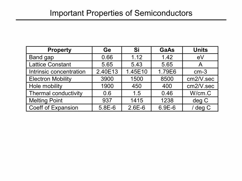
Important Properties of Semiconductors
Property Ge Si GaAs Units Band gap 0.66 1.12 1.42 eV Lattice Constant 5.65 5.43 5.65 A Intrinsic concentration 2.40E13 1.45E10 1.79E6 cm-3 Electron Mobility 3900 1500 8500 cm2/V.sec Hole mobility 1900 450 400 cm2/V.sec Thermal conductivity 0.6 1.5 0.46 W/cm.C Melting Point 937 1415 1238 deg C Coeff of Expansion 5.8E-6 2.6E-6 6.9E-6 / deg C

Strained Layer SiGe Epitaxy
Ge 5.65 Ao
Si 5.43 Ao
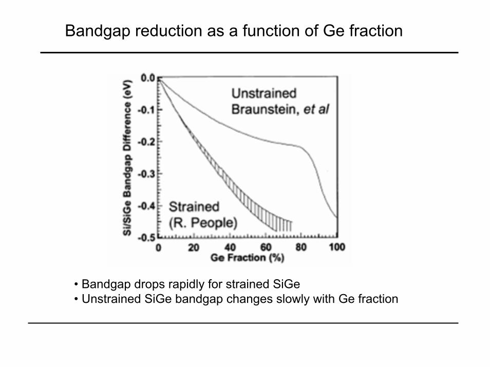
Bandgap reduction as a function of Ge fraction
• Bandgap drops rapidly for strained SiGe• Unstrained SiGe bandgap changes slowly with Ge fraction
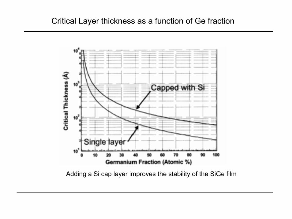
Critical Layer thickness as a function of Ge fraction
Adding a Si cap layer improves the stability of the SiGe film

Comparing MOS and Single Poly Bipolar
BIPOLARMOS
CG E
S D BB
STI STI
P+ S/D Implant
PLDD Implant
Gate oxide
Gate Poly
Spacer
STISTI STI
BL
SNK
Emitter Poly
P+ Ext base Implant P Link Implant
Shallow Trench
N+ Buried Layer
Sinker
N type epi
Intrinsic base Implant
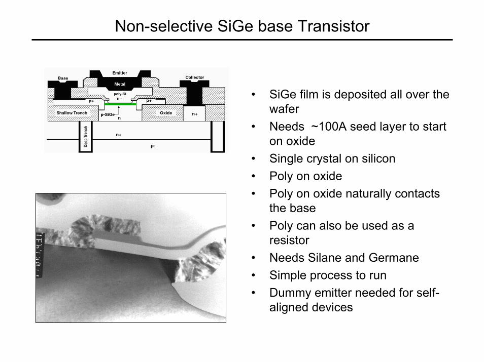
Non-selective SiGe base Transistor
• SiGe film is deposited all over the wafer
• Needs ~100A seed layer to start on oxide
• Single crystal on silicon• Poly on oxide• Poly on oxide naturally contacts
the base• Poly can also be used as a
resistor• Needs Silane and Germane• Simple process to run• Dummy emitter needed for self-
aligned devices

SEM Cross section of a SiGe Bipolar Transistor

Selective SiGe base Transistor
• SiGe grows on exposed regions of the Si wafer
• Oxide is used as a mask• No need for a seed layer• Needs DCS, HCl and Germane• Sensitive to exposed pattern
density• Low throughput• Additional poly is needed to
contact the base• Integrates into an existing double
poly process
Nitride spacer
cavity
sel SiGe
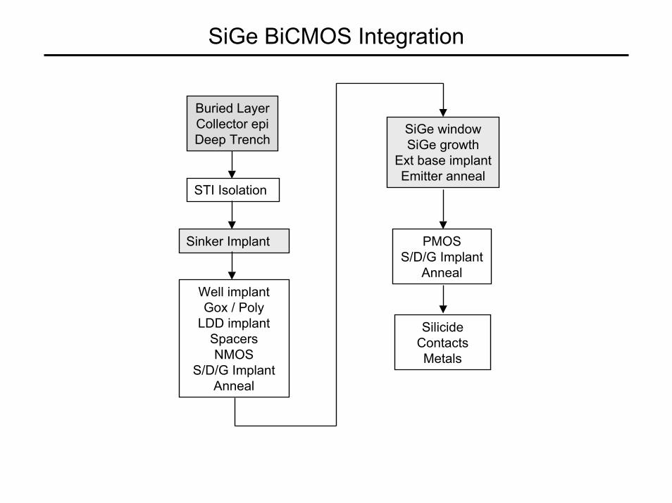
SiGe BiCMOS Integration
Buried LayerCollector epiDeep Trench
STI Isolation
Sinker Implant
Well implantGox / Poly
LDD implantSpacersNMOS
S/D/G ImplantAnneal
SiGe windowSiGe growth
Ext base implantEmitter anneal
PMOS S/D/G Implant
Anneal
SilicideContactsMetals
Why add Carbon to SiGe base?
• The thin boron doped base diffuses during thermal processing widening the base and degrading the fT
• B diffuses with an interstitial Si atom generated by unoptimized epi, oxidation, implantation etc.
• C can take on the interstitial Si sites suppressing B diffusion• C being a smaller atom, the strain due to Ge can be reduced• Less strain means less dislocations and less diffusion• C has to be substitutional instead of interstitial• Solubility of C in Si is low, some go into interstitial sites• Substitutional C can be evaluated by XRD.

Effect of Carbon on Boron Diffusion
0.2% C

Uniformity of Device Results
Ic (Amps)VBE (volts) IBM data
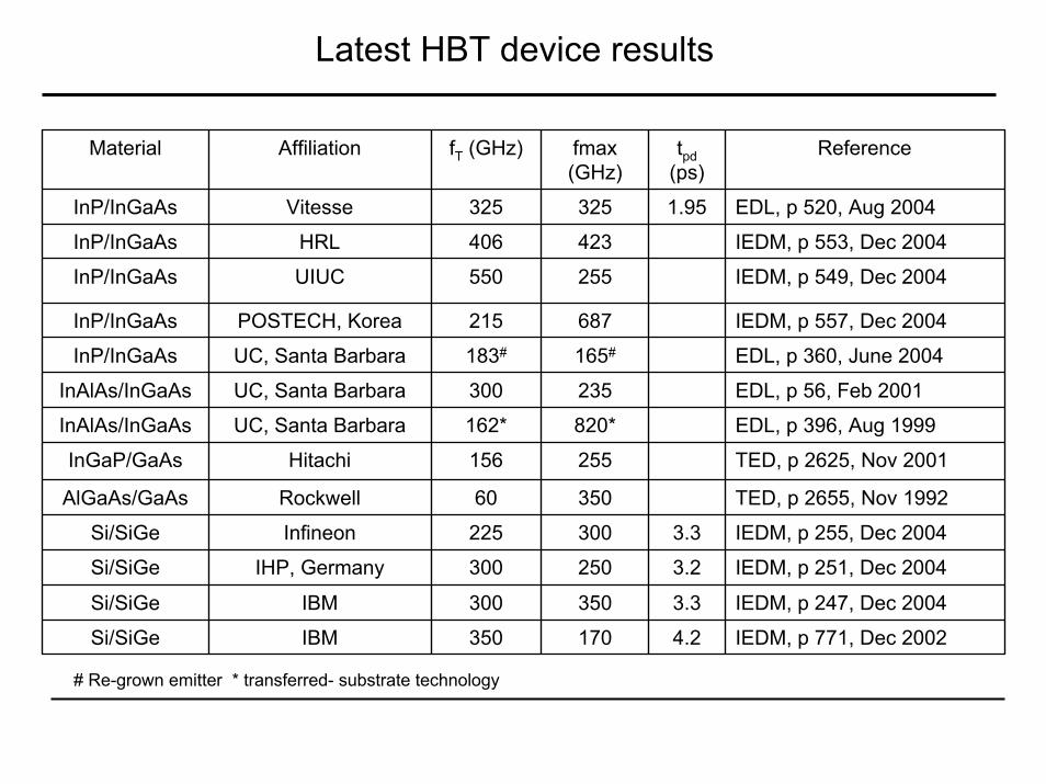
Latest HBT device results
TED, p 2655, Nov 199235060RockwellAlGaAs/GaAs
IEDM, p 771, Dec 20024.2170350IBMSi/SiGe
IEDM, p 247, Dec 20043.3350300IBMSi/SiGe
IEDM, p 251, Dec 20043.2250300IHP, GermanySi/SiGe
IEDM, p 255, Dec 20043.3300225InfineonSi/SiGe
TED, p 2625, Nov 2001255156HitachiInGaP/GaAs
EDL, p 396, Aug 1999820*162*UC, Santa BarbaraInAlAs/InGaAs
EDL, p 56, Feb 2001235300UC, Santa BarbaraInAlAs/InGaAs
EDL, p 360, June 2004165#183#UC, Santa BarbaraInP/InGaAs
IEDM, p 557, Dec 2004687215POSTECH, KoreaInP/InGaAs
IEDM, p 549, Dec 2004255550UIUCInP/InGaAs
IEDM, p 553, Dec 2004423406HRLInP/InGaAs
EDL, p 520, Aug 20041.95325325Vitesse InP/InGaAs
Referencetpd(ps)
fmax (GHz)
fT (GHz)AffiliationMaterial
# Re-grown emitter * transferred- substrate technology

SiGe HBT Noise Figure Data from IBM
Fmin
GA
Ft = 200GHz, Ae=0.12x64µ2 Greenberg et al., IEDM 2002, pp. 787-790.

BVCEO – fT Curve – Johnson Limit
510GHzVBVCEO . Ft product
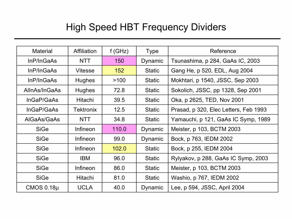
High Speed HBT Frequency Dividers
Bock, p 255, IEDM 2004Static102.0InfineonSiGe
Lee, p 594, JSSC, April 2004Dynamic40.0UCLACMOS 0.18µ
Washio, p 767, IEDM 2002Static81.0HitachiSiGe
Meister, p 103, BCTM 2003 Static86.0InfineonSiGe
Rylyakov, p 288, GaAs IC Symp, 2003Static96.0IBMSiGe
Bock, p 763, IEDM 2002Dynamic99.0InfineonSiGe
Meister, p 103, BCTM 2003Dynamic110.0InfineonSiGe
Yamauchi, p 121, GaAs IC Symp, 1989 Static34.8NTTAlGaAs/GaAs
Prasad, p 320, Elec Letters, Feb 1993Static12.5TektronixInGaP/GaAs
Oka, p 2625, TED, Nov 2001Static39.5HitachiInGaP/GaAs
Sokolich, JSSC, pp 1328, Sep 2001Static72.8HughesAlInAs/InGaAs
Mokhtari, p 1540, JSSC, Sep 2003Static>100HughesInP/InGaAs
Gang He, p 520, EDL, Aug 2004Static152VitesseInP/InGaAs
Tsunashima, p 284, GaAs IC, 2003Dynamic150NTTInP/InGaAs
ReferenceTypef (GHz)AffiliationMaterial

Infineon SiGe 1:32 Static Divider running at 102 GHz
50mV/div
100ps
J. Bock et al., Infineon, 3.3ps SiGe technology, IEDM 2004. pp 255-258.

Principle of Dynamic Frequency Dividers
3/2 f in
1/2 f in 1/2 f inf inLPF
1/2 f in
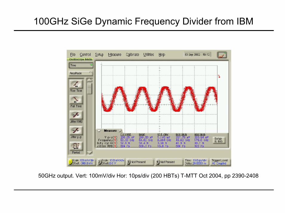
100GHz SiGe Dynamic Frequency Divider from IBM
50GHz output. Vert: 100mV/div Hor: 10ps/div (200 HBTs) T-MTT Oct 2004, pp 2390-2408
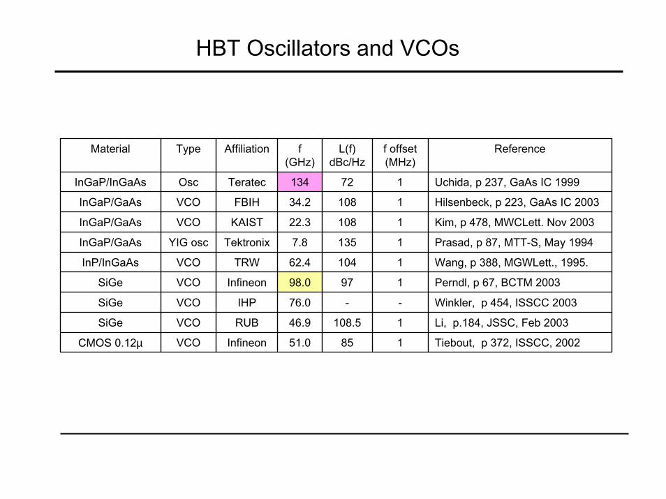
HBT Oscillators and VCOs
Tiebout, p 372, ISSCC, 200218551.0InfineonVCOCMOS 0.12µ
Li, p.184, JSSC, Feb 2003 1108.546.9RUBVCOSiGe
Winkler, p 454, ISSCC 2003 --76.0IHPVCOSiGe
Perndl, p 67, BCTM 200319798.0InfineonVCOSiGe
Wang, p 388, MGWLett., 1995.110462.4TRWVCOInP/InGaAs
Prasad, p 87, MTT-S, May 199411357.8TektronixYIG oscInGaP/GaAs
Kim, p 478, MWCLett. Nov 2003110822.3KAISTVCOInGaP/GaAs
Hilsenbeck, p 223, GaAs IC 2003110834.2FBIHVCOInGaP/GaAs
Uchida, p 237, GaAs IC 1999172134TeratecOscInGaP/InGaAs
Referencef offset (MHz)
L(f)dBc/Hz
f (GHz)
AffiliationTypeMaterial

33GHz SiGe Voltage Controlled Oscillator

HBT Power Transistors and Amplifiers
Bakalski, p 61, BCTM 2003111417.57-18InfineonPASiGe
Pan, p 209, BCTM 20043612820IBMPA Vcc=1.1SiGe 200GHz
Nellis, p1751, JSSC, Oct 200433.122.1281.88SkyworksPower AmpSi (27GHz)
Nellis, p1751, JSSC, Oct 20043521.8281.88SkyworksPower AmpSiGe (44GHz)
Nellis, p1751, JSSC, Oct 200439.327.1281.88SkyworksPower AmpInGaP 46GHz
Kurpas, p 561, IEDM 20047114412FBIHPower HBTInGaP/GaAs
Potyraj, p 2392, T-MTT, Nov 1996466.953.62.8NorthropPower HBT SiGe
Shimura, p 1890, TED, Nov 19957263012MitsubishiPower HBTAlGaAs/GaAs
Yang, p 1455, T- MTT, May 20044027280.837SkyworksIS95B PAInGaP/GaAs
Kim, p 905, JSSC, June 20034028281.9KAISTWCDMA paInGaP/GaAs
Handa, p.227, GaAs IC, 2003-1513.060SharpPower AmpInGaP/GaAs
Liu, p.215, EDL, June 199452731.83TIPower HBTInGaP/GaAs
ReferencePAE %
GaindB
Pout(dBm)
f (GHz)AffiliationTypeMaterial

HBT Low Noise Amplifiers
K.Yu, p 106, MWCLett., March 20045.612.924UCLALNACMOS 0.18m
He, p 956, JSSC, June 2004614.50.1-23UIUCDA LNASiGe
Gramegna, p 49, BCTM 20031.6228.2STMicroLNASiGe
Ellinger, p 702, Trans. MTT, Feb 20043.814.516ETHVG LNASiGe
Urteaga, p 1452, JSSC, Sep 20038.5140-220UCSBWideband AmpInP/InGaAs
ReferenceNFdB
GaindB
f (GHz)AffiliationTypeMaterial
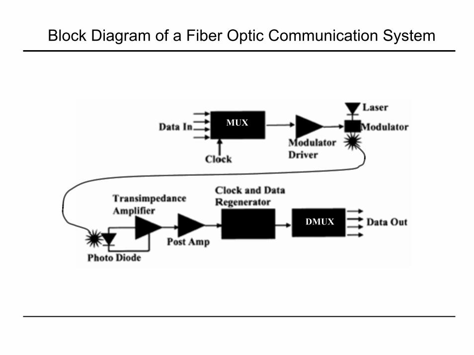
Block Diagram of a Fiber Optic Communication System
MUX
DMUX

HBT Digital Communication Circuits
Rieh, JSSC, p 2390, Oct 200470.0IBM4:1MUXSiGe
J. Lee, JSSC, p 2181, Dec 200340.0UCLACDR/ 1:4 DMUXCMOS 0.18µ
Kehrer, JSSC, p 1830, Nov 200340.0Infineon2:1 MUX/DMUXCMOS 0.12µ
Felder, JSSC, p 481, April 199650.0Siemens2:I MUXSi bipolar
Weiner, JSSC, p 1512, Sep 200340.0LucentTIASiGe
Meghelli, JSSC, p 2147, Dec 200343.0IBMCDR- Rx/TxSiGe
Meghelli, JSSC, p 1790, Dec 200250.0IBM4:1 MUX/DMUXSiGe
C.Wu, JSSC, p 1518, Sep 200340.0VitesseTIAInP/InGaAs
Hendarman, JSSC, p 1497, Sep 200340.0Vitesse16:1 MUXInP/InGaAs
Nielsen, JSSC, p 2341, Dec 200343.2InphiCDR/DMUXInP/InGaAs
Ishii, MWCLett., p 2181, Nov 200340.0NTT4:1 MUX/DMUXInP/InGaAs
ReferenceSpeed (Gb/sec)
AffiliationCircuitMaterial

OC768 40Gb/s 16:1 MUX and 1:16 DMUX
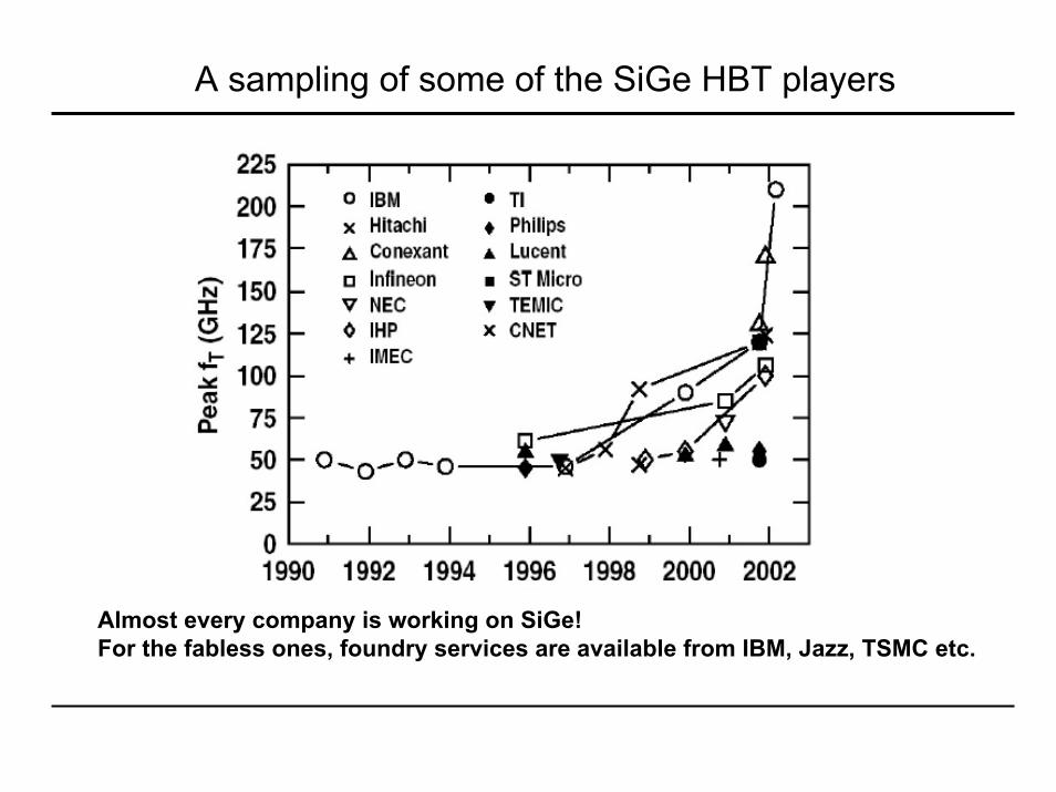
A sampling of some of the SiGe HBT players
Almost every company is working on SiGe!For the fabless ones, foundry services are available from IBM, Jazz, TSMC etc.

Conclusion
• Presented the SiGe device physics• Discussed SiGe material properties• Integration of SiGe into bipolar/BiCMOS• Showed device results• Talked about circuit applications• Demonstrated the future potential of SiGe


![HORIZONTAL CURRENT BIPOLAR TRANSISTOR (HCBT) A …performance Si/SiGe BiCMOS technologies [4] prohibitively expensive. On the other hand, Horizontal Current Bipolar Transistor (HCBT)](https://static.fdocuments.net/doc/165x107/5eb51a6ba40ea3329e0dbf95/horizontal-current-bipolar-transistor-hcbt-a-performance-sisige-bicmos-technologies.jpg)