Sidechannel Resistant Lightweight ASIC Implementations of ... · i Abstract In this thesis, we...
87
Sidechannel Resistant Lightweight ASIC Implementations of DES and AES Diplomarbeit by Axel Poschmann Department of Electrical Engineering and Information Sciences Ruhr-Universit¨ at Bochum Chair for Communication Security (COSY) Supervisor: Prof. Dr.-Ing. Christof Paar Dipl.-Ing. Kai Schramm Beginning: June 6th 2005 End: December 5th 2005
Transcript of Sidechannel Resistant Lightweight ASIC Implementations of ... · i Abstract In this thesis, we...

Sidechannel Resistant Lightweight ASIC
Implementations of DES and AES
Diplomarbeit
by
Axel Poschmann
Department of Electrical Engineering and Information Sciences
Ruhr-Universitat Bochum
Chair for Communication Security (COSY)
Supervisor: Prof. Dr.-Ing. Christof Paar
Dipl.-Ing. Kai Schramm
Beginning: June 6th 2005
End: December 5th 2005

Erklarung
Hiermit versichere ich, dass ich meine Diplomarbeit selbst verfaßt und keine anderen als
die angegebenen Quellen und Hilfsmittel benutzt sowie Zitate kenntlich gemacht habe.
I hereby certify that the work presented in this thesis is my own work and that to the
best of my knowledge it is original except where indicated by reference to other authors.
Axel Poschmann
Ort, Datum

i
Abstract
In this thesis, we investigate a new lightweight cipher based on DESX. We investigate
the design criteria of DES presented in [Cop94] and derive stronger design criteria. We
show that S-boxes, which satisfy our new design criteria are more resistant against both
differential and linear cryptanalysis. Our new cipher DLX is similar to DES or DESX,
respectively, except for the f -function. DES uses eight different S-boxes, whereas our
cipher only repeatedly uses one improved S-box (eight times).
The implementation results show that our new cipher DLX requires less chip size,
less energy, and is more secure against both differential and linear cryptanalysis. We
also show that DLX requires 40% less chip size, 85% less clock cycles, and consumes
only about 10% of the energy than the best AES implementation with regard to RFIDs
needs [FDW04].
In this thesis we also investigate side channel attacks on AES. We present a size-
optimised VHDL design of the AES and its results for a standard cell implementation.
We show, that this ASIC can easily be broken with a simple power analysis (SPA).
Keywords:
side channel attacks, simple power analysis (SPA), differential power analysis (DPA),
finite fields, composite fields, application specific integrated circuit (ASIC), standard cell
design, VHDL, very large scale design (VLSI), mos current mode logic (MCML), CML,
Advanced Encryption Standard (AES), Data Encryption Standard (DES), DESX, DLX,
radio frequency identification (RFID), S-box, design criteria, differential cryptanalysis,
linear cryptanalysis, lightweight

ii
Acknowledgement
There are a lot of people who I would like to thank. All of them helped me to succeed
in writing this diploma thesis. That is, why I would like to say: Danke Kai Schramm
for your great job in supervising me. Danke Gregor Leander for your mathematical
skills and your patience when trying to explain. Danke Christof Paar, Tesekkurler Yusuf
Leblebici and Grazie Paolo Ienne for the coordination of the whole project. Thank you
Matt Robshaw for your advices concernig mathematical properties of S-boxes. Toda Eli
Biham for your advices concerning S-box properties. Danke Johann Großschadl for the
power simulation. Dank je well Theo Kluter for teaching me VHDL. Merci Alain Vachoux
for your great ”Top-down digital design flow” documentation and your help concerning
the setup of EDA tools etc. Dhan-ya-vaad Aniket Singh for your work concerning placing
and routing of the differential chip. Danke Benedikt Gierlichs, Philipp Sudmeyer, and
Sven Schage for proof-reading this thesis. And finally, Thank you to all the others I
bothered with questions during the last six months!

Contents
1 Introduction 1
2 A New Hardware Approach Against Differential Power Analysis Attacks 3
2.1 Mathematical Basics . . . . . . . . . . . . . . . . . . . . . . . . . . . . . 3
2.1.1 Finite Fields . . . . . . . . . . . . . . . . . . . . . . . . . . . . . . 3
2.1.2 Isomorphic Mapping . . . . . . . . . . . . . . . . . . . . . . . . . 4
2.2 Introduction to the Advanced Encryption Standard . . . . . . . . . . . . 5
2.2.1 Encryption . . . . . . . . . . . . . . . . . . . . . . . . . . . . . . 5
2.2.2 Decryption . . . . . . . . . . . . . . . . . . . . . . . . . . . . . . 9
2.3 Introduction to Power Analysis Attacks . . . . . . . . . . . . . . . . . . . 11
2.3.1 Simple Power Analysis . . . . . . . . . . . . . . . . . . . . . . . . 13
2.3.2 Differential Power Analysis . . . . . . . . . . . . . . . . . . . . . . 13
2.3.3 Countermeasures against Power Analysis Attacks . . . . . . . . . 14
2.4 Introduction to MCML . . . . . . . . . . . . . . . . . . . . . . . . . . . . 14
2.5 A Size Optimised VHDL Model of the AES . . . . . . . . . . . . . . . . 15
2.5.1 A Size Optimised S-box Implementation . . . . . . . . . . . . . . 16
2.5.2 The Modules . . . . . . . . . . . . . . . . . . . . . . . . . . . . . 20
2.5.3 Datapath . . . . . . . . . . . . . . . . . . . . . . . . . . . . . . . 32
2.6 Implementation of the AES in CMOS . . . . . . . . . . . . . . . . . . . . 34
2.6.1 VLSI Design Flow for a Standard Cell ASIC . . . . . . . . . . . . 34
2.6.2 Performance of the CMOS AES ASIC . . . . . . . . . . . . . . . 36
2.7 Simple Power Analysis on AES . . . . . . . . . . . . . . . . . . . . . . . 36
2.8 Conclusion and Future Works . . . . . . . . . . . . . . . . . . . . . . . . 39
3 A Compact New DESX Variant 40
3.1 Introduction to the Data Encryption Standard . . . . . . . . . . . . . . . 40
3.2 Design Criteria of the DES S-boxes . . . . . . . . . . . . . . . . . . . . . 43
3.3 Improved Design Criteria . . . . . . . . . . . . . . . . . . . . . . . . . . . 45
3.3.1 Improved Criteria (S-2’) and (S-2”) . . . . . . . . . . . . . . . . . 47

Contents iv
3.3.2 Improved Criterion (S-6’) . . . . . . . . . . . . . . . . . . . . . . 49
3.3.3 Improved S-box . . . . . . . . . . . . . . . . . . . . . . . . . . . . 49
3.4 DLX - A Modified Lightweight DESX Variant . . . . . . . . . . . . . . . 50
3.4.1 Description of DLX . . . . . . . . . . . . . . . . . . . . . . . . . . 50
3.4.2 Cryptographic Aspects of DLX . . . . . . . . . . . . . . . . . . . 51
3.5 A size-optimised VHDL Design of DESX and DLX . . . . . . . . . . . . 58
3.5.1 The Modules . . . . . . . . . . . . . . . . . . . . . . . . . . . . . 59
3.5.2 The Datapath . . . . . . . . . . . . . . . . . . . . . . . . . . . . . 63
3.5.3 VHDL Design of DLX . . . . . . . . . . . . . . . . . . . . . . . . 65
3.6 Implementations of DESX and DLX . . . . . . . . . . . . . . . . . . . . 65
3.6.1 Implementation of DESX . . . . . . . . . . . . . . . . . . . . . . . 68
3.6.2 Implementation of DLX . . . . . . . . . . . . . . . . . . . . . . . 69
3.7 DESX versus DLX . . . . . . . . . . . . . . . . . . . . . . . . . . . . . . 71
4 Conclusion and Future Works 72
4.1 Concerning Our Work on the AES . . . . . . . . . . . . . . . . . . . . . 72
4.2 Concerning Our Work on the DES . . . . . . . . . . . . . . . . . . . . . 72

List of Figures
2.1 Isomorphism between GF(28) and GF((24)2) . . . . . . . . . . . . . . . . 4
2.2 Input, State array, and output . . . . . . . . . . . . . . . . . . . . . . . 5
2.3 Encryption order of the AES-128 . . . . . . . . . . . . . . . . . . . . . . 6
2.4 SubBytes . . . . . . . . . . . . . . . . . . . . . . . . . . . . . . . . . . . 7
2.5 ShiftRows . . . . . . . . . . . . . . . . . . . . . . . . . . . . . . . . . . . 7
2.6 MixColumns . . . . . . . . . . . . . . . . . . . . . . . . . . . . . . . . . . 8
2.7 Structure of the KeyExpansion . . . . . . . . . . . . . . . . . . . . . . . 9
2.8 Decryption order of the AES-128 . . . . . . . . . . . . . . . . . . . . . . 10
2.9 InvSubBytes . . . . . . . . . . . . . . . . . . . . . . . . . . . . . . . . . . 10
2.10 InvShiftRows . . . . . . . . . . . . . . . . . . . . . . . . . . . . . . . . . 11
2.11 InvMixColumns . . . . . . . . . . . . . . . . . . . . . . . . . . . . . . . . 11
2.12 CMOS inverter . . . . . . . . . . . . . . . . . . . . . . . . . . . . . . . . 12
2.13 Transistor-level view of the generic CML gate . . . . . . . . . . . . . . . 15
2.14 Architecture of the Composite Field S-box implementation . . . . . . . . 17
2.15 Composite Field mapping entities . . . . . . . . . . . . . . . . . . . . . . 18
2.16 Composite Field entities . . . . . . . . . . . . . . . . . . . . . . . . . . . 18
2.17 Input and Output of the AES ASIC . . . . . . . . . . . . . . . . . . . . . 21
2.18 Architecture of the memory module . . . . . . . . . . . . . . . . . . . . . 22
2.19 S-box for 8-bit wide input . . . . . . . . . . . . . . . . . . . . . . . . . . 23
2.20 Dataflow of InvMixColumns . . . . . . . . . . . . . . . . . . . . . . . . . 26
2.21 Architecture of the keymanagement module . . . . . . . . . . . . . . . . 27
2.22 Finite state machine of the controller module . . . . . . . . . . . . . . . . 31
2.23 Overall architecture of the ASIC . . . . . . . . . . . . . . . . . . . . . . . 33
2.24 Top-Down VLSI design flow for standard cells . . . . . . . . . . . . . . . 35
2.25 Layout of the AES ASIC . . . . . . . . . . . . . . . . . . . . . . . . . . . 37
2.26 Schematic of the first five clockcycles . . . . . . . . . . . . . . . . . . . . 37
2.27 Powertrace of 128 Encryptions . . . . . . . . . . . . . . . . . . . . . . . . 38
3.1 Structure of the DES Cipher . . . . . . . . . . . . . . . . . . . . . . . . . 41

List of Figures vi
3.2 Structure of Keyscheduling of DES Cipher. . . . . . . . . . . . . . . . . . 42
3.3 Principle of DESX . . . . . . . . . . . . . . . . . . . . . . . . . . . . . . 43
3.4 Structure of the f -function of DLX . . . . . . . . . . . . . . . . . . . . . 51
3.5 2 round characteristic in DES . . . . . . . . . . . . . . . . . . . . . . . . 57
3.6 Input and Output of the DESX ASIC . . . . . . . . . . . . . . . . . . . . 60
3.7 Finite State Machine of the DESX ASIC . . . . . . . . . . . . . . . . . . 61
3.8 Datapath of the DESX . . . . . . . . . . . . . . . . . . . . . . . . . . . . 66
3.9 Datapath of the DLX . . . . . . . . . . . . . . . . . . . . . . . . . . . . . 67
3.10 Layout of the DESX ASIC . . . . . . . . . . . . . . . . . . . . . . . . . . 69
3.11 Layout of the DLX ASIC . . . . . . . . . . . . . . . . . . . . . . . . . . . 70

List of Tables
2.1 Classification scheme of DPA countermeasures . . . . . . . . . . . . . . . 14
2.2 Implementation results of the AES ASIC . . . . . . . . . . . . . . . . . . 36
3.1 Leftshift offset for each round of DES . . . . . . . . . . . . . . . . . . . . 42
3.2 Maximum values concerning criterion (S-7) of DES S-boxes . . . . . . . . 45
3.3 For criterion (S-8) maximum probabilities for collisions at single S-box
outputs . . . . . . . . . . . . . . . . . . . . . . . . . . . . . . . . . . . . 46
3.4 Maximum probabilities dj of collisions in S-box triplets for 32-bit input
differentials ∆mj . . . . . . . . . . . . . . . . . . . . . . . . . . . . . . . 46
3.5 Maximum values concerning criterion (S-2’) of DES S-boxes . . . . . . . 48
3.6 Improved DLX S-box . . . . . . . . . . . . . . . . . . . . . . . . . . . . . 50
3.7 Comparison of DES and DLX S-box(es) . . . . . . . . . . . . . . . . . . 51
3.8 P function and P−1 function of DES . . . . . . . . . . . . . . . . . . . . 65
3.9 Number of transistors necessary for some standard gates . . . . . . . . . 65
3.10 Results of DESX, built in 0.18 µm CMOS . . . . . . . . . . . . . . . . . 68
3.11 Results of DLX, built in 0.18 µm CMOS . . . . . . . . . . . . . . . . . . 70
4.1 Comparison based on power consumption, gate count, and clock cycles . 73

1 Introduction
Since global competition is intensifying, companies are forced to cut costs. The usage of
information technologies can help to reach this goal in many different ways. For example
Radio Frequency IDentification tags (from now on referred to as RFID) can improve the
efficiency of the logistic chain significantly.
Companies which want to be successful in the global competition, permanently need
an advantage in technology. Thus these companies have to spend a lot of money on
research. The gained research results represent a very valuable good for them - and
for their competitors. Intensifying global competition implies also the rise of economic
warfare. This means that companies may use espionage, amongst other illegal or semi-
legal methods, to gain access to confidential information of their competitors (for example
research results). Countermeasures against espionage are for example access control to
buildings and computers, authentication of users, and encryption of stored data and
communication.
Authentication also plays a role for the successful use of RFID tags. To prevent that
the data stored in an RFID chip can be read out by spies or for surveillance, only
authenticated RFID readers should be allowed to gain access. Authentication can be
achieved by cryptographic measures. Because RFID chips are passive devices, they have
a limited power supply. Furthermore, the price of the RFID chip correlates directly with
the size of the used ASIC (Application Specific Integrated Circuit). Hence, a lightweight
encryption core is desired.
One goal of this diploma thesis is the development of a low-power, size-optimised,
lightweight encryption engine, suitable for the use in an RFID chip. In Chapter 3 we
present a new variant of the Data Encryption Standard (DES) [Nat99], that fulfills all
these properties. We improve the design criteria of the original DES S-boxes and derive
new design criteria. S-boxes are generated with regard to these new design criteria. From
this set, we choose an S-box with the best cryptographic properties and the smallest
chip size. DES uses eight different S-boxes for substitution, whereas our approach uses
only one S-box repeated eight times. We show, that our new DLX (DES Lightweight
eXtension) cipher is smaller in chip size while being even more resistant against both
linear cryptanalysis [Mat94] and differential cryptanalysis [BS91] than DES. To thwart

Introduction 2
exhaustive key search, we applied prewhitening and postwhitening, like proposed in DESX
[KR01], resulting in a keyspace of 2184 possible keys.
Another topic of this diploma thesis deals with side channel attacks and their coun-
termeasures. The most common side channel attack is the Differential Power Analysis
(further referred to as DPA). If smart cards are unprotected against DPA, it is possible
to reveal the secret key by measuring and analyzing the power consumption [KJJ99].
The second goal of this diploma thesis is to design a side channel-resistant hardware
implementation of the Advanced Encryption Standard (AES) [Nat01]. There are many
different approaches to thwart DPAs like masking [Eli04], time de-synchronisation or
adding uncorrelated noise. These approaches only try to conceal the signal dependency
of the power consumption at the algorithmic or architectural level. The origin of the
signal dependency is at the logic level and that is where our approach applies. The
differential MOS Current Mode Logic (MCML) library is based on a special logic style,
called Current Mode Logic (CML). ASICs, which are build in MCML, have a plain power
consumption and hence, are ideally immune against power analysis attacks.
The remainder of this diploma thesis is organised as follows: In Chapter 2, a new hard-
ware approach against power analysis attacks is presented. Starting with some mathe-
matical basics in Section 2.1, we give an introduction to the cipher Advanced Encryption
Algorithm (AES) [Nat01] in Section 2.2. Subsequently, an introduction to side channel
attacks and their countermeasures is given in Section 2.3. In Section 2.4, we give a brief
introduction to MCML. A VHDL design of the AES is presented in Section 2.5 and its
implementation results in Section 2.6. After we show how the AES ASIC can be broken
with simple power analysis in Section 2.7 we finish this chapter with a conclusion in
Section 2.8.
In Chapter 3, a new lightweight DES variant is presented. Starting with an introduc-
tion to the Data Encryption Standard (DES) in Section 3.1, we recapitulate the design
criteria of DES in Section 3.2. Subsequently, we derive stronger design criteria in Sec-
tion ?? and investigate the new DLX cipher in Section 3.4. A size-optimised VHDL
design of DESX and DLX is presented in Section 3.5 and the corresponding implemen-
tation results in Section 3.6. Finally, in Section 3.7, we summarise our results of this
chapter.
This thesis is completed by a conclusion in Chapter 4.
2 A New Hardware Approach Against
Differential Power Analysis Attacks
Since Paul Kocher et al. first presented Differential Power Analysis (DPA) in [KJJ99],
a lot of research has been done to prevent such attacks. All these approaches are either
not successful or only fix the symptoms. Our approach goes further. We try to prevent
DPA at the circuit level instead of fighting the symptoms.
The remainder of this chapter is structured as follows: first, we present some math-
ematical basics in Section 2.1. Subsequently, we give an introduction to the AES in
Section 2.2. Then, in Section 2.3, an introduction to power analysis attacks is given,
followed by an introduction to MOS Current Mode Logic (MCML) in Section 2.4. In
Section 2.5 a size-optimised VHDL design of the AES is presented. The implementation
of this design with standard CMOS cells is presented in Section 2.6. Finally, we success-
fully attack this implementation with an SPA in Section 2.7 and finish with a conclusion
in Section 2.8.
2.1 Mathematical Basics
In this section the necessary mathematical basics are presented. Starting with a short
introduction to finite field representations and arithmetic operations in GF(28) in Sec-
tion 2.1.1, the concept of isomorphic mappings will be presented in the following Sec-
tion 2.1.2.
2.1.1 Finite Fields
In the AES algorithm all bytes are interpreted as finite field elements using the following
polynomial representation: GF (28) = GF (2)[x]m(x)
, where m(x) = x8 +x4 +x3 +x+1 denotes
an irreducible polynomial of degree 8. Then:

2.1 Mathematical Basics 4
GF (28)I7−→ GF (28)
φ ↓ ↑ φ−1
GF (24)2 I′7−→ GF (24)
2
Figure 2.1: Isomorphism between GF(28) and GF((24)2)
b7x7 + b6x
6 + b5x5 + b4x
4 + b3x3 + b2x
2 + b1x1 + b0x
0 =7∑
i=0
bixi, bi ∈ GF (2)
where bi denotes the i-th coefficient of the polynomial.
Addition of two polynomials is done by adding the polynomials modulo 2, because the
coefficients are elements of {0,1}. Thus the XOR operation (denoted by ⊕) can be used
for addition. This also implies, that substraction of polynomials is identical to addition.
The irreducible polynomial m(x) of degree 8 ensures that the result of a multiplication
in GF(28) will be a binary polynomial of degree less than 8. Thus the result can be
represented as a byte. The multiplicative inverse element is defined by the following
equation:
a(x)b(x) mod m(x) = 1 ⇒ a(x) = b−1(x) mod m(x)
For further mathematical details see [DR02].
2.1.2 Isomorphic Mapping
The finite field GF(28) can be written as the quadratic extension of the finite field
GF(24): GF(28) = GF((24)2). An isomorphic mapping φ bijectively maps from GF(28)
to GF((24)2) and an inverse isomorphic mapping φ−1 maps back to GF(28), as it is
depicted in Figure 2.1. In the AES, the inverse operation I is performed during SubBytes.
I maps from GF(28) to GF(28). The composite fields approach exploits the fact, that
the inverse operation in GF((24)2) I’ can be realised much more efficiently in hardware
than the inverse operation in GF(28) I.

2.2 Introduction to the Advanced Encryption Standard 5
Figure 2.2: Input, State array, and output
2.2 Introduction to the Advanced Encryption Standard
In November 2001 the Rijndael algorithm was chosen as the Advanced Encryption Stan-
dard (AES) by the National Institute of Standards and Technology (NIST) as the suc-
cessor of the Data Encryption Standard (DES) (see [Nat01], [DR02], and [Nat99] for
details). It is a symmetric block cipher, that processes datablocks of 128 bits. Three
different keylengths are possible: 128, 192, and 256 bits, resulting in 10, 12 or 14 rounds
for the cipher, respectively. AES is, depending on the keylength, also referred to as AES-
128, AES-192, and AES-256. Because the chip developed during this diploma thesis uses
AES-128, the remainder of this document only describes AES with a keylength of 128
bit and hence a round number of 10.
At the beginning of the algorithm, the input is copied into the State array (also called
State), which consists of 16 bytes, arranged in four rows and four columns (4 x 4 -
Matrix, see Figure 2.2). At the end, the State array is copied to the output.
The bytes of the State are interpreted as coefficients of a polynomial representation
of finite field elements in GF (28). All byte values in the remainder of this document will
be written in hexadecimal notation.
2.2.1 Encryption
In encryption mode, the initial key is added to the input value at the very beginning,
which is called an initial round. This is followed by 9 iterations of a normal round and
ends with a slightly modified final round, as one can see in Figure 2.3.
During one normal round the following operations are performed in the following order:
SubBytes, ShiftRows, MixColumns, and AddRoundkey. The final round is a normal round
without the MixColumns stage.

2.2 Introduction to the Advanced Encryption Standard 6
AddRoundKey
MixColumns
AddRoundKey
ShiftRows
SubBytes
AddRoundKey
Initial Round Normal Round Final Round
9 x
SubBytes
ShiftRowsCiphertextPlaintext
Figure 2.3: Encryption order of the AES-128
SubBytes
This is a nonlinear, invertible byte substitution using the so called S-Box (see Figure 2.4).
Two transformations are performed on each of the bytes independently:
� First each byte is substituted by its multiplicative inverse in GF (28) (if existent),
element {00} is mapped to itself.
� Then the following affine transformation over GF (2) is applied:
b′i = bi ⊕ b(i+5)mod8 ⊕ b(i+6)mod8 ⊕ b(i+7)mod8 ⊕ ci
for 0 ≤ i ≤ 8, where bi(ci) is the i-th bit of the byte b(c). c = 6316 = 011000112
The affine transformation can be written as the following matrix:
b′0b′1b′2b′3b′4b′5b′6b′7
=
1 0 0 0 1 1 1 1
1 1 0 0 0 1 1 1
1 1 1 0 0 0 1 1
1 1 1 1 0 0 0 1
1 1 1 1 1 0 0 0
0 1 1 1 1 1 0 0
0 0 1 1 1 1 1 0
0 0 0 1 1 1 1 1
b0
b1
b2
b3
b4
b5
b6
b7
+
1
1
0
0
0
1
1
0
ShiftRows
As the Figure 2.5 depicts, the ShiftRows operation cyclically shifts each row of the State
by a certain offset. The first row is not shifted at all, the second row is shifted by one,
the third row by two, and the fourth row by three bytes to the left.

2.2 Introduction to the Advanced Encryption Standard 7
Figure 2.4: SubBytes
Figure 2.5: ShiftRows
MixColumns
The columns of the State are processed one at a time during this operation. The bytes
are interpreted as coefficients of a four-term polynomial over GF (24). Each column is
multiplied modulo x4+1 with a fixed polynomial a(x) = {03}x3+{01}x2+{01}x+{02}.This can be written as the following matrix multiplication, where s′(x) = a(x)⊗ s(x):
S ′0,c
S ′1,c
S ′2,c
S ′3,c
=
02 03 01 01
01 02 03 01
01 01 02 03
03 01 01 02
S0,c
S1,c
S2,c
S3,c
for 0 ≤ c ≤ 3.
As one can see in Figure 2.6 the columns of the State are processed independently of
one another.
AddRoundKey
This operation adds the 128-bit round key generated from KeyExpansion to the 128-bit
State. It is a simple XOR-addition of the round key and the State.

2.2 Introduction to the Advanced Encryption Standard 8
Figure 2.6: MixColumns
KeyExpansion
For a complete AES encryption or decryption 10 round keys are needed. The KeyEx-
pansion derives them from the initial key iteratively as it is depicted in Figure 2.7. The
key is grouped into four words w0, w1, w2, and w3, that consist of four bytes each.
The pseudocode of KeyExpansion is as follows:
KeyExpansion ( byte key [ 4 * 4 ] , word w[ 4* ( 1 0+1 ) ] , 4 )begin
word tempi = 0while ( i < 4)
w[ i ] = word ( key [4* i ] , key [4* i +1 ] , key [4* i +2 ] , key [4* i +3])i = i+1
end whilei = 4while ( i < 4 * (10+1) ]
temp = w[ i −1]i f ( i mod 4 = 0)
temp = SubWord(RotWord( temp ) ) xor rcon [ i /4 ]end i fw[ i ] = w[ i −4] xor tempi = i + 1
end whileend
The fourth word of the initial key (w3) is cyclically shifted to the left by one byte. The
result is bytewise substituted by the S-Box. Afterwards a round constant is XOR-added.
This new value results after an XOR-addition with the old first word w0 in the new
first word w′0. The new second word w′
1 is derived from this new first word w′0 by an

2.2 Introduction to the Advanced Encryption Standard 9
Figure 2.7: Structure of the KeyExpansion
XOR-addition with the old second word w1 and so on. These new four words form the
next round key, from which the following round keys are derived in the same manner.
Thus the fourth word of the round key is cyclically shifted, bytewise substituted and so
on.
The round constants rconi are derived by the following equation:
rconi = xi mod m(x),
where i denotes the roundnumber, 0 ≤ i ≤ 9 and the irreducible polynomial m(x)=
x8 + x4 + x3 + x + 1. This means, that the new round constant can be calculated from
the old one just by a multiplication with x. For the first eight round constants this
corresponds with a simple leftshift. In decryption mode the order of the round keys
is inverse to their order in encryption mode. This means, that the first round key in
decryption mode is the last round key of encryption mode and vice versa.
2.2.2 Decryption
In decryption mode, the operations are in reverse order compared to their order in
encryption mode (see Figure 2.8). Thus it starts with an initial round, followed by 9

2.2 Introduction to the Advanced Encryption Standard 10
AddRoundKey
AddRoundKey
Initial Round Normal Round Final Round
9 x
AddRoundKey
InvMixColumns
InvShiftRows
InvSubBytes
InvShiftRows
InvSubBytes
Inverse Inverse
PlaintextCiphertext
Inverse
Figure 2.8: Decryption order of the AES-128
Figure 2.9: InvSubBytes
iterations of an inverse normal round and ends with an AddRoundKey. An inverse normal
round consists of the following operations in this order: AddRoundKey, InvMixColumns,
InvShiftRows, and InvSubBytes. An initial round is an inverse normal round without the
InvMixColumns.
InvSubBytes
This is the inverse operation of SubBytes. As it is depicted in Figure 2.9, InvSubBytes
operates bytewise on the State. First the inverse of the affine transformation is applied
to each byte, followed by the substitution with its multiplicative inverse in GF (28).
InvShiftRows
This is the inverse of the ShiftRows operation. The second row is cyclically shifted by one
byte to the right, the third row by two, and the fourth row by three bytes respectively.
Figure 2.10 illustrates the InvShiftRows transformation.
2.3 Introduction to Power Analysis Attacks 11
Figure 2.10: InvShiftRows
Figure 2.11: InvMixColumns
InvMixColumns
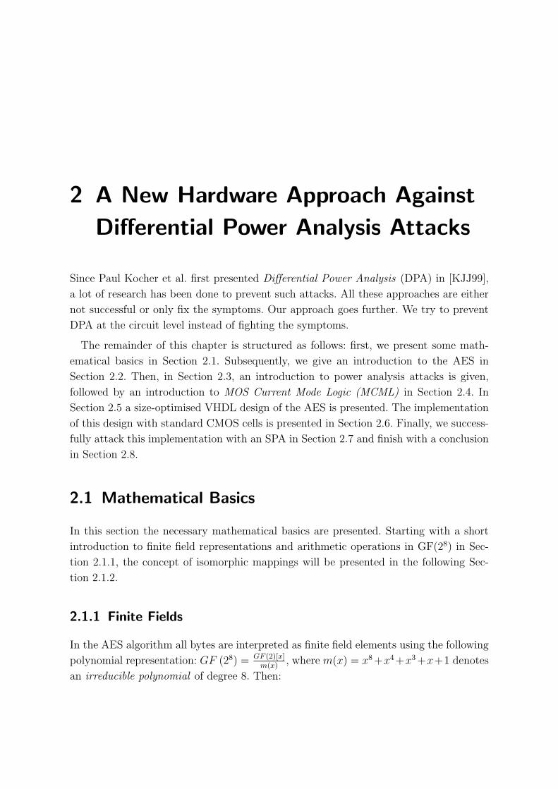
This is the inverse of the MixColumns operation. As it is depicted in Figure 2.11 each
column of the State is multiplied modulo x4 + 1 with a fixed polynomial a−1(x) =
{0b}x3 + {0d}x2 + {09}x + {0e}. This can be written as the following matrix multipli-
cation, where s′(x) = a−1(x)⊗ s(x):
S ′0,c
S ′1,c
S ′2,c
S ′3,c
=
0e 0b 0d 09
09 0e 0b 0d
0d 09 0e 0b
0b 0d 09 0e
S0,c
S1,c
S2,c
S3,c
for 0 ≤ c ≤ 3.
2.3 Introduction to Power Analysis Attacks
In this section, we present a few basics about side channel attacks, especially power
analysis attacks.
Even though modern ciphers like AES seem to be resistant against cryptographic
attacks, such as linear or differential cryptanalysis, it might be possible to attack the

2.3 Introduction to Power Analysis Attacks 12
Input Output
Vdd
Vss
Figure 2.12: CMOS inverter
implementation of the algorithm, if it is implemented in a straightforward manner. In
the last years it became clear, that any implementation of a cryptographic system can
leak sensitive information about processed key-related data. The term side channel sum-
marises all possible ways of collecting this information, such as processing time[Koc96],
power consumption [KJJ99][AO][KJJ99] or electromagnetic emission [AK96].
Nearly all digital circuits are build in Complementary Metal Oxide Semiconductor
(CMOS) technology, because this technology is efficient regarding power-consumption,
chip size and clock frequency. With other words: it is the cheapest way to build small
and fast integrated circuits.
In Figure 2.12, a simple CMOS inverter consisting of a p-channel Metal Oxide Semi-
conductor PMOS and an n-channel Metal Oxide Semiconductor NMOS transistor is
depicted.
CMOS circuits have many advantages in terms of chip size, costs and speed, but they
also have significant disadvantages regarding power analysis attacks, because CMOS
gates have a state-dependent power consumption. This can be used to gain knowledge
about the currently processed data, by measuring the power consumption of a gate. It
is possible to determine whether a CMOS gate changes its state or not from a power
trace. With synchronous integrated circuits this is even worse, because all gates switch
their state at the same time. Thus, the sum of all switched states is a significant source
of leakage of the circuit.
In this thesis, we will focus on power analysis attacks like Simple Power Analysis
(SPA) and Differential Power Analysis (DPA), because they are the easiest ones to
implement, and thus the most promising for an attacker.
Power analysis attacks are known-plaintext attacks. Hence, an attacker needs access
to the plaintext and furthermore, he needs passive physical access to the target device
to collect the power traces.
In the remainder of this section we will introduce simple power analysis in Section 2.3.1
and differential power analysis in Section 2.3.2. Subsequently, we will discuss possible
countermeasures against power analysis attacks in Section 2.3.3.
2.3 Introduction to Power Analysis Attacks 13
2.3.1 Simple Power Analysis
In SPA, an attacker measures the power consumption and deduces information either
by the Hamming weight leakage or by transition count leakage1 [MDS99]. The Hamming
weight leakage describes the fact, that the amount of current is directly proportional to
the Hamming weight of the processed data. Hence it is possible to derive the processed
data. This is described by the term transition count leakage.
The simplicity of this approach is bounded by two disadvantages. First, SPA is strongly
hardware dependent. And second, the attacker has to know the exact point of time when
the information, he wants to deduce, is processed.
2.3.2 Differential Power Analysis
For DPA, an attacker does not need information about the analysed hardware nor about
the points in time, when the desired information is processed. Furthermore, uncorrelated
(white) noise superposed to measurements is filtered out. All this makes DPA more
powerful than SPA.
First, an attacker has to measure the power consumption of the cryptographic device
during encryption of many known plaintexts. For each encryption an attacker guesses the
state of a chosen key-dependent intermediate selected function based on a key hypothesis.
Next, the attacker computes the correlation coefficient of the measured power traces and
the outcomes of the selected function. Only if the key hypothesis is correct, correlation
peaks will occur.
When power consumption of any device is measured, the gained results always include
noise. Together with the assumption, that the power consumption of a circuit P (t) is the
sum of power consumptions of gates, we can derive the following simple power model:
P (t) =∑
g
f (g, t) + N (t) ,
where f (g, t) denotes the power consumption of a gate g at the time t and N (t) denotes
a uncorrelated normally distributed random variable representing the noise components.
For further details see [AO]. The only disadvantage of DPA, compared to SPA, is its
higher complexity.
1i.e., Hamming distance

2.4 Introduction to MCML 14
Level Approach
Algorithmic Time De-synchronisation, Masking
Architectural Adding Noise
Logic Alternative Logic Styles
Table 2.1: Classification scheme of DPA countermeasures
2.3.3 Countermeasures against Power Analysis Attacks
The proposed countermeasures against power analysis attacks can be classified in ap-
proaches at the algorithmic, architectural, or logic level (see Table 2.1).
Time de-synchronisation can be achieved by randomly halting the processor for one or
more cycles. As a consequence, an attacker needs to measure the power consumption of
much more plaintexts, because the power traces are not synchronised anymore. Hence,
no peak will appear. [C. 00] shows a way to resynchronize the power traces. Masking
modifies the algorithm in a way, that a randomly generated value is XORed with the
input of the S-box. Later in the algorithm, another proper calculated value is XORed to
compensate the modification, like described in [Eli04]. Mangard et al. showed in [S. 05],
that masking could not thwart power analysis attacks on their masked AES ASIC im-
plementations due to glitches. Adding noise to the power consumption merely lowers the
side channel information and might be disabled by tampering.
All mentioned approaches only try to conceal the signal dependency of the power
consumption at the algorithmic or architectural level. The origin of the signal dependency
is at the logic level and that is where our approach applies.
2.4 Introduction to MCML
MOS current mode logic (MCML) is a circuit configuration with differential input and
differential output. The operation in current mode logic (CML)
is based on the principle of re-directing (or switching) the current of a con-
stant current source through a fully differential network of input transistors,
and utilizing the reduced-swing voltage drop on a pair of complementary load
devices as the output ([I. 05]).
Figure 2.132 depicts a generic CML gate. Originally, CML was invented for very high-
2Source: [I. 05].

2.5 A Size Optimised VHDL Model of the AES 15
Figure 2.13: Transistor-level view of the generic CML gate
speed circuits, because it offers robust operation, reduced power supply, and improved
immunity against process variations [Pay03]. CML also provides an input-independent
power consumption. This is very attractive with regard to power analysis attacks, because
hereby the fact that a major part of the power consumption of CMOS circuits arises
from gate switching is exploited.
2.5 A Size Optimised VHDL Model of the AES
The Applicaton Specific Integrated Circuit (ASIC) was designed in VHDL. VHDL is
shortform for Very high speed integrated circuit Hardware Description Language. Its
development was initiated by the Department of Defense of the United States of America
in 1983 and became an IEEE standard in 1987 (IEEE.1076). To get started with VHDL
we used [Smi97], [Bha99], [Mae], and [AG00] among many other tutorials like for instance
[Gla] etc. A good reference are also the slides of the course Architecture des Ordinateurs
[Ien] at the Ecole Polytechnique Federale de Lausanne.
The presented VHDL design is suitable both for encryption as well as for decryption
with a keylength of 128 bits3. No special modes like Cipher-Block-Chaining (CBC),
Cipher-Feed-Back (CFB), Output-Feed-Back (OFB) or Counter (CTR) are supported.
For any hardware design there is always a tradeoff between area and speed. The faster
a chip is, the more area is needed and vice versa. This VHDL design is size-optimised
but with an eye on the speed.
3Parts of this section are a further development of the results from my Studienarbeit [Pos05].

2.5 A Size Optimised VHDL Model of the AES 16
2.5.1 A Size Optimised S-box Implementation
As briefly introduced in Section 2.1, it is possible to calculate the inverse not in GF(28)
but in GF((24)2). In [WOL02] this fact is exploited and a size-optimised S-box imple-
mentation of the AES is designed. This approach uses the Composite Field method. Its
architecture with its various modules is depicted in Figure 2.14.
Isomorphic Mapping
The number of needed gates of the operations in GF(24) depends directly on the irre-
ducible polynomial. In [WOL02] the following polynomial is stated as the simplest, and
hence the best for a size-optimised design:
GF((
24)2
)' GF (2) [x]
x2 + x + e
First, an Isomorphic Mapping T : GF (28) 7→ GF ((24)2) has to be determined. This
transformation T has to satisfy the following equations:
al0
al1
al2
al3
ah0
ah1
ah2
ah3
= T
a0
a1
a2
a3
a4
a5
a6
a7
Wolkerstorfer et al. chose the following transformation for the isomorphic mapping:
T =
1 0 0 0 1 1 1 0
0 1 1 0 0 0 0 0
0 1 0 0 0 0 0 1
0 0 1 0 1 0 0 0
0 0 0 0 1 1 1 0
0 1 0 0 1 0 1 1
0 0 1 1 0 1 0 1
0 0 0 0 0 1 0 1
We use the symbol depicted in Figure 2.15 (a).

2.5 A Size Optimised VHDL Model of the AES 17
Figure 2.14: Architecture of the Composite Field S-box implementation

2.5 A Size Optimised VHDL Model of the AES 18
map
4 4
8
ah al
(a) isomorphic map-
ping
inverse map
8
4 4 ah’ al’
(b) inverse isomorphic
mapping
Figure 2.15: Composite Field mapping entities
4
4 4
(a) addition
4
4
4
(b) multiplication
x*x
4
4
(c) squaring
1/x
4
4
(d) inverse
Figure 2.16: Composite Field entities

2.5 A Size Optimised VHDL Model of the AES 19
Inverse Isomorphic Mapping
The inverse isomorphic mapping: T−1GF ((24)2) 7→ GF (28) has to satisfy the following
equation:
a0
a1
a2
a3
a4
a5
a6
a7
= T−1
al0
al1
al2
al3
ah0
ah1
ah2
ah3
Again, we adopted the transformations chosen by Wolkerstorfer et al.. It is:
T−1 =
1 0 0 0 1 0 0 0
0 0 0 0 1 1 0 1
0 1 0 0 1 1 0 1
0 1 0 0 1 1 1 0
0 1 0 1 1 1 0 1
0 0 1 0 1 1 0 0
0 1 1 1 1 0 0 1
0 0 1 0 1 1 0 1
The symbol we used is depicted in Figure 2.15 (b).
Operations in GF(24)
In GF(24) a different irreducible polynomial is used than in GF(28). It is:
GF(24
) ' GF (2) [x]
x4 + x + 1
Addition, multiplication, inversion, and squaring can be implemented very efficient in
GF(24). The symbols used for these operations are depicted in Figure 2.16.
For further details the interested reader is referred to [WOL02].

2.5 A Size Optimised VHDL Model of the AES 20
2.5.2 The Modules
The overall architecture of the ASIC is shown in Figure 2.17. It consists of the mod-
ules Memory, SubBytes, MixColumns, InverseMixColumns, Controller, and KeyMan-
agement, as well as five multiplexors, and three XORs.
As one can see from Figure 2.17 our chip has the following input and output signals:
� Input signals
clk clocks the chip
n reset resets the chip. This flag is active low.
encrypt specifies the mode of operation. If set to 1 the chip encrypts, otherwise
the chip decrypts.
enable starts the algorithm. Must be set to 1 just at the very beginning of each
128 bit block.
input is a 128 bit wide input bus. This data will be processed by the ASIC either
as plaintext to encrypt or as ciphertext to decrypt.
key is a 128 bit wide input bus. The key is read only after the chip is reset.
� Output signals
output is a 128 bit wide output bus. The result of the encryption / decryption
will be sent to this bus.
done is a flag, that shows if the output is valid or not.
entity top i sport (
c l k : in s t d l o g i c ;n r e s e t : in s t d l o g i c ;encrypt : in s t d l o g i c ;enable : in s t d l o g i c ;input : in s t d l o g i c v e c t o r (127 downto 0 ) ;key : in s t d l o g i c v e c t o r (127 downto 0 ) ;output : out s t d l o g i c v e c t o r (127 downto 0 ) ;done : out s t d l o g i c) ;
end entity top ;

2.5 A Size Optimised VHDL Model of the AES 21
Sub-
Bytes
Mix-
Columns
Key-
Manage-
ment
Inverse-
Mix-
Columns
Con-
troller Memory
CLK
n_reset
encrypt
enable
input[128]
key[128]
output[128]
done
Figure 2.17: Input and Output of the AES ASIC
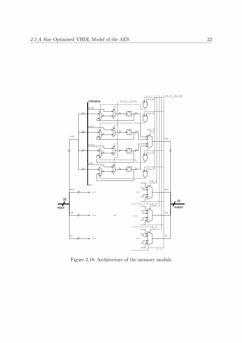
Memory
The Memory module stores the State after each round. Input signals are: clk, reset,
rd 0, rd 1, rd 2, rd 3, ctrl init, ctrl hold, initvalue, and input. Output signals are output
and lastoutput. Below is the VHDL code of the entity declaration:
entity memory i sport (
c l k : in s t d l o g i c ;r e s e t : in s t d l o g i c ;rd 0 : in s t d l o g i c v e c t o r ( 1 downto 0 ) ;rd 1 : in s t d l o g i c v e c t o r ( 1 downto 0 ) ;rd 2 : in s t d l o g i c v e c t o r ( 1 downto 0 ) ;rd 3 : in s t d l o g i c v e c t o r ( 1 downto 0 ) ;c t r l i n i t : in s t d l o g i c ;c t r l h o l d : in s t d l o g i c ;i n i t v a l u e : in s t d l o g i c v e c t o r (127 downto 0 ) ;input : in s t d l o g i c v e c t o r (31 downto 0 ) ;output : out s t d l o g i c v e c t o r (31 downto 0 ) ;l a s t ou tput : out s t d l o g i c v e c t o r (127 downto 0 )) ;
end entity memory ;
The structure of 16 bytesized d-flip-flops allows it to address each byte of the State
independently. As one can see in Figure 2.18, the four multiplexors on the right side allow
the selection of four bytes of the State, which are combined to a 32-bit wide output of
this module. The output multiplexors are controlled by the control signals rd 0, rd 1,
rd 2, and rd 3, selecting each one byte out of a row of the State. This architecture
allows to implement the ShiftRows and the InvShiftRows operations by using proper
addressing.
2.5 A Size Optimised VHDL Model of the AES 22
D Qrst
D Qrst
D Qrst
D Qrst
[31:24]
[23:16]
[15:8]
[7:0]
...
...
...
...
...
...
...
[31:24]
[23:16]
[15:8]
[7:0]
0
1
3
2
0
1
3
2
0
1
3
2
0
1
3
2
[95:0]
initvalue
[127:120]
[103:96]
[119:112]
[111:104]
ctrl_initrd_0 = "00"
rd_0 = "01"
rd_0 = "10"
rd_0 = "11"
32
1
01
0
1
01
0
1
01
0
1
01
0
8
8
8
8
8
8
8
8
8
8
8
8
8
8
8
8
8
8
8
8 8
ctrl_holdctrl_hold
ctrl_hold
outputinput
� 32
rd_0
rd_1
rd_2
rd_3
Figure 2.18: Architecture of the memory module

2.5 A Size Optimised VHDL Model of the AES 23
SubBytes
The SubBytes module wires four identical S-boxes, each substituting 8 bits. The S-
boxes are implemented in the way it was proposed by Wolkerstorfer et al. in [WOL02].
The main trick in this approach is that the inverse is not computed in GF(28), but in
GF((24)2). Instead of implementing the inverse calculation by a look-up-table with 256
(16× 16) bytes, just combinatorial logic is needed to calculate the inverse.
Input and output signals are encrypt, input, and output (see VHDL code below).
entity sbox i sport (
encrypt : in s t d l o g i c ;input : in s t d l o g i c v e c t o r (31 downto 0 ) ;output : out s t d l o g i c v e c t o r (31 downto 0 )) ;
end entity sbox ;
During decryption first the inverse affine transformation is applied before the inverse
is calculated, while during encryption the affine transformation is applied after the in-
verse calculation. For that reason, this module has two multiplexors, one before inverse
calculation and one after it, enabling it to perform SubBytes as well as InvSubBytes (see
Figure 2.19).
affine transition
inverse affine transition
1 0
1 0
inverse
encrypt input 8
8 output
Figure 2.19: S-box for 8-bit wide input
Inside the inverse block first the isomorphic mapping from GF(28) to GF((24)2) is
performed then the input is transformed. Then, the inverse in GF((24)2) is calculated.

2.5 A Size Optimised VHDL Model of the AES 24
Afterwards, another modular multiplication and finally the mapping from GF((24)2) to
GF(28) is performed. For further details see [WOL02] and [Rij].
Because this S-box is suitable for both encryption and decryption, the required chip
size is reduced to nearly 25 % in comparison to an implementation with a normal look-
up table. Another advantage is the possibility to synthesize this design with differential
cells, which is important for the MCML ASIC.
MixColumns
This module has the input signal in vec and the output signal out vec (see VHDL code
below).
entity mixcolumns i sport (
i n vec : in s t d l o g i c v e c t o r (31 downto 0 ) ;out vec : out s t d l o g i c v e c t o r (31 downto 0 )) ;
end entity mixcolumns ;
Starting from the matrix presented in Section 2.2.1, one can derive a system of equa-
tions, which is much better suited for implementation. After substituting Sx′ and Sx by
ax′ and ax one get:
a0′ = {02}a0 + {03}a1 + {01}a2 + {01}a3 = xa0 + (x + 1)a1 + a2 + a3
a1′ = {01}a0 + {02}a1 + {03}a2 + {01}a3 = a0 + xa1 + (x + 1)a2 + a3
a2′ = {01}a0 + {01}a1 + {02}a2 + {03}a3 = a0 + a1 + xa2 + (x + 1)a3
a3′ = {03}a0 + {01}a1 + {01}a2 + {02}a3 = (x + 1)a0 + a1 + a2 + xa3
After reordering and substituting + by ⊕ and multiplications by ⊗ one can derive the
following equations:
a0′ = (x⊗ (a0 ⊕ a1))⊕ a1 ⊕ a2 ⊕ a3
a1′ = (x⊗ (a1 ⊕ a2))⊕ a0 ⊕ a2 ⊕ a3
a2′ = (x⊗ (a2 ⊕ a3))⊕ a0 ⊕ a1 ⊕ a3

2.5 A Size Optimised VHDL Model of the AES 25
a3′ = (x⊗ (a3 ⊕ a0))⊕ a0 ⊕ a1 ⊕ a2
The MixColumns module implements the matrix multiplication with the following
equations:
t = a0 ⊕ a1 ⊕ a2 ⊕ a3
a0′ = a0 ⊕ (x⊗ (a0 ⊕ a1))⊕ t
a1′ = a1 ⊕ (x⊗ (a1 ⊕ a2))⊕ t
a2′ = a2 ⊕ (x⊗ (a2 ⊕ a3))⊕ t
a3′ = a3 ⊕ (x⊗ (a3 ⊕ a0))⊕ t
where ai represents the i-th byte of the input value (column), i = 0...3, ⊕ represents
a bitwise XOR-addition, and ⊗ represents a multiplication with {x} in GF(28) modulo
m(x) = x8 + x4 + x3 + x + 1. A multiplication with {x} corresponds to a simple leftshift
of the binary representation, where the least significant bit is filled with 0 and the
most significant bit is discarded. If the most significant bit is 1, an additional modular
reduction is necessary. This can be done by XOR-adding 00011011 - which is the binary
representation of the irreducible polynomial m(x)= x8 + x4 + x3 + x + 1 - to the result
of the leftshift.
InverseMixColumns
As one can see from the VHDL code fragment below, the InverseMixColumns module
has in vec as input and out vec as output.
entity imixcolumns i sport (
i n vec : in s t d l o g i c v e c t o r (31 downto 0 ) ;out vec : out s t d l o g i c v e c t o r (31 downto 0 )) ;
end entity imixcolumns ;
The matrix in Section 2.2.2 can be split into the following two matrices:
0e 0b 0d 09
09 0e 0b 0d
0d 09 0e 0b
0b 0d 09 0e
=
05 00 04 00
00 05 00 04
04 00 05 00
00 04 00 05
02 03 01 01
01 02 03 01
01 01 02 03
03 01 01 02

2.5 A Size Optimised VHDL Model of the AES 26
Due to the fact, that the elements of the matrices are coefficients of a polynomial over
GF(28), + corresponds to ⊕ (XOR) and a multiplication to ⊗ (modular multiplication).
The InverseMixColumns module performs the first matrix transformation on the input
values, such that they can afterwards be processed by the MixColumns module (see
Figure 2.20). The first matrix on the right hand side can be expressed by the following
equations:
u = x⊗ x⊗ (a0 ⊕ a2)
v = x⊗ x⊗ (a1 ⊕ a3)
a0′ = a0 ⊕ u
a1′ = a1 ⊕ v
a2′ = a2 ⊕ u
a3′ = a3 ⊕ v
where ai represents the i-th byte of the input value (column), i = 0...3, ⊕ represents
a bitwise XOR-addition and ⊗ represents a multiplication with x in GF(28) modulo
m(x) = x8 + x4 + x3 + x + 1.
InvMixColumns MixColumns
Figure 2.20: Dataflow of InvMixColumns
AddRoundKey
Due to the fact, that AddRoundKey is a simple XOR, it is not implemented as a module.
As one can see in Figure 2.23, there are three XORs in the datapath. The first one is
in the upper left corner, right before the Memory module. This is the AddRoundkey in
the initial round both during encryption as well as during decryption. The second XOR,
in front of InvMixColumns is used in a normal round in decryption as well as in final
round of both encryption and decryption. The XOR in the lower left corner is used by
a normal round during encryption.

2.5 A Size Optimised VHDL Model of the AES 27
Figure 2.21: Architecture of the keymanagement module

2.5 A Size Optimised VHDL Model of the AES 28
KeyManagement
As shown in Figure 2.21 the KeyManagement module consists of three major parts: in
the upper left corner the initial key is stored (Key flip-flop), in the lower part the round
constant (rcon) is computed, and in the middle part the round key is computed.
Input and output signals are shown in the following VHDL code fragment.
entity keymanagement i sport (
c l k : in s t d l o g i c ;n r e s e t : in s t d l o g i c ;c t r l r s t : in s t d l o g i c ;c t r l e n c r yp t : in s t d l o g i c ;load key : in s t d l o g i c ;c t r l k s : in s t d l o g i c ;c t r l k e y : in s t d l o g i c ;c t r l i n i t : in s t d l o g i c ;key : in s t d l o g i c v e c t o r (127 downto 0 ) ;sb out : in s t d l o g i c v e c t o r (31 downto 0 ) ;k s sb i n : out s t d l o g i c v e c t o r (31 downto 0 ) ;roundkey : out s t d l o g i c v e c t o r (31 downto 0 ) ;i n i t k e y : out s t d l o g i c v e c t o r (127 downto 0 )
) ;
end entity keymanagement ;
The round constant is computed ”on-the-fly” by the following equation:
xi = xi mod x8 + x4 + x3 + x + 1,
where i = 0...9 denotes the round number. This function is implemented in the timesx -
component and is performed only in the first cycle of a normal round. When in decryption
mode, the rcon-flip-flop is initialised with ”36”, which is the last round constant, otherwise
it is initialised with ”01”. In decryption mode the round constants have to be divided by
two, which is nearly always a simple right shift (represented by the ”À”-component in the
diagram). But when the round constant has to be modulo reduced, this is implemented
by the multiplexor at the bottom. When the last two bits of rcon are both 1, then the
next d rcon is ”80”.
The initial key is loaded into the key flip-flop in the initial clockcycle. At the beginning
of each block-processing the 128-bit output of the key flip-flop is split to four 32-bit wide

2.5 A Size Optimised VHDL Model of the AES 29
flip-flops. When in decryption mode, the last round key is computed and stored in the
key-flip-flop (not the initial key!).
During encryption in the first clockcycle of a normal round the output of flip-flop
number ”0” (keybits[31:0]) is cyclically leftshifted by eight bits, then substituted by the
S-box, the round constant rcon is XOR-added, and finally the output of flip-flop number
”3” is XOR-added. This is the new input of flip-flop number ”3”. For that reason the
ctrl ks-signal has to be set to 1. All other flip-flops hold the old values, thus the signals
ctrl ks2, ctrl ks1, and ctrl ks0 are set to 0. In this clockcycle no round key is needed,
because the S-box was blocked by the KeyManagement.
In the second clockcycle the first round key is provided and the second round key is
computed. Both is achieved when ctrl ks2 and ctrl ks d1 are 1 while all other ctrl ks-
signals are 0. In each clockcycle the last computed round key is provided and the following
round key is computed. For this reason the initial ctrl ks-signal is delayed by four flip-
flops in a row. This architecture allows that only at the beginning of each round the
ctrl ks-signal must be set to 1, while all other ctrl ks-signals are derived from this.
Controller
The controller module manages all control signals in the ASIC based on the finite state
machine. The input and output signals are shown in the following VHDL code fragment:
entity c o n t r o l l e r i sport (
c l k : in s t d l o g i c ;n r e s e t : in s t d l o g i c ;enable : in s t d l o g i c ;encrypt : in s t d l o g i c ;c t r l e n c r yp t : out s t d l o g i c ;load key : out s t d l o g i c ;c t r l k e y : out s t d l o g i c ;c t r l i n i t : out s t d l o g i c ;c t r l k s : out s t d l o g i c ;c t r l r s t : out s t d l o g i c ;c t r l l a s t r o und : out s t d l o g i c ;rd 0 : out s t d l o g i c v e c t o r ( 1 downto 0 ) ;rd 1 : out s t d l o g i c v e c t o r ( 1 downto 0 ) ;rd 2 : out s t d l o g i c v e c t o r ( 1 downto 0 ) ;rd 3 : out s t d l o g i c v e c t o r ( 1 downto 0 ) ;aes done : out s t d l o g i c

2.5 A Size Optimised VHDL Model of the AES 30
) ;
end entity c o n t r o l l e r ;
All output signals are control signals for the other modules. Below is a list of all control
signals and their function:
ctrl encrypt is needed during the keyscheduling. The first round key in decryption mode
is the last one in encryption mode. Hence all round keys have to be calculated before
the first round starts, which needs a positive encrypt flag. Because the encrypt flag
is false in decryption mode, the ctrl encrypt signal is necessary.
load key loads key flip-flop with initial key.
ctrl key controls the intput of key flip-flop. It is only needed to save the last round key
computed during keyscheduling in decryption mode.
ctrl init loads the initial input values into the memory flip-flops and the key into the
round key flip-flops.
ctrl ks controls the output of the KeyManagement module. At the same time it controls
the input of the round key flip-flops.
ctrl rst initialises nearly all flip-flops and counters with zero. This is done for example
for each new input block of 128 bits.
ctrl lastround bypasses the InvMixColumns and MixColumns module both in encryp-
tion and decryption mode.
rd 0 selects one byte of the 1st row of the State.
rd 1 selects one byte of the 2nd row of the State.
rd 2 selects one byte of the 3rd row of the State.
rd 3 selects one byte of the 4th row of the State.
aes done controls the output of the chip. If and only if this flag is positive the output
is valid, otherwise it is zero or undefined.
In Figure 2.22 the finite state machine (FSM) of the controller module is shown. It
consists of the following eight states:

2.5 A Size Optimised VHDL Model of the AES 31
Figure 2.22: Finite state machine of the controller module
IDLE, INIT ONCE, INIT KEY ONCE, INIT KEY, INIT BLOCK, INIT ROUND,
ROUND, and DONE.
Whenever reset is set to 0 the state is switched to IDLE. The transition from this state
to the INIT ONCE state is only possible when enable is set to 1. In the INIT ONCE
state all operations are performed, which are only required once after changing the key
or switching from decryption to encryption mode, for example reading the key.
The INIT KEY ONCE and its successor INIT KEY are only performed when the
ASIC decrypts(encrypt set to 0). In these two states the last round key is computed by
ten times iterating a normal keyscheduling. This is required, because this design has no
memory to store the round keys, which saves a lot of space.
In encryption as well as in decryption mode the remaining order of the states is the
same. INIT BLOCK is the next state. Here, all operations which are only required
once per 128-bits-block are performed, for instance loading the input into the memory.
After one clockcycle the transition to INIT ROUND is done, where all operations are
performed which are required once per round, for instance the use of the S-box by the
KeyManagement. In the ROUND state, each column is processed and when a counter
reaches three (meaning that all four columns are processed) the FSM goes back to the
INIT ROUND state. This is repeated until a counter reaches 10, meaning that all 10
rounds are performed. Then the FSM transits to the DONE state. When enable is set
to 1 the next state is INIT BLOCK else the FSM stays in the DONE state.

2.5 A Size Optimised VHDL Model of the AES 32
2.5.3 Datapath
The SubBytes and the ShiftRows (and their respective inverse) operations are commu-
tative. Thus, it is possible to swap the order of these operations.
The MixColumns operation needs at least one column of the State for computation,
while the ShiftRows operation needs at least one row of the State. For that reason
the ShiftRows as well as the InverseShiftRows operation is implemented by address
calculation. In comparison to wiring, this decision allows a 32-bit wide datapath instead
of a 128-bit wide datapath, which considerably reduces the area required. This comes at
a cost of four clock cycles to perform the transformations of one round on the 128-bit
State.
Because the KeyManagement also uses the SubBytes module, an additional clockcycle
is needed for the calculation of the round key.
Encryption
As depicted in Figure 2.23 the datapath of a normal encryption round is given by the
signals out mem, in sb, out sb, in mc, out mc, s in mem, and in mem. Thus the control
signals for the multiplexors ctrl ks and ctrl lastround must be set to 0 and encrypt must
be set to 1.
The datapath of the final round in encryption mode consists of the signals out mem,
in sb, out sb, in imc, and in mem. The control signals have the same value as during a
normal round except for the ctrl lastround signal, which must be set to 1.
Decryption
The SubBytes module implements both SubBytes and InvSubBytes. Due to the fact,
that the order of InvSubBytes and InvShiftRows is swapped and that the InvShiftRows
is implemented with address calculation, the order of a normal round in decryption
mode now is InvSubBytes, AddRoundKey, and InvMixColumns (see Figure 2.23). In the
InvMixColumns module the input data is transformed such that the normal MixColumns
module can be used.
As one can see in Figure 2.23 all this is exploited by using the same SubBytes and
MixColumns modules. The input value for the MixColumns are controlled by the encrypt
signal.
During a normal round in decryption mode, the datapath consists of the signals
out mem, in sb, out sb, in imc, out imc, in mc, out mc, s in mem, and in mem. There-
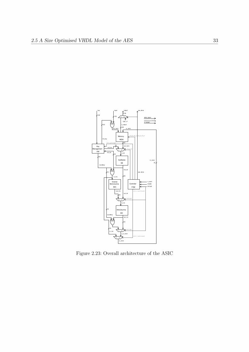
2.5 A Size Optimised VHDL Model of the AES 33
key
ManagementKey
KM
Memory
MEM
Controler
FSM
SubBytes
SB
MixColumns
MC
out_mem
init_key
init_mem
input
s_output
in_mem
in_mem
in_mem
s_in_mem
in_imc
in_imc
in_mc
out_imc
out_mc
roundkey
roundkey
in_sb
out_sb
out_sb
output
"000...0"
aes_done
aes_done
enable
n_reset
encrypt
ctrl_lastround
ctrl_lastround
encrypt
encrypt
ctrl_ks
rd_0,rd_1,rd_2,rd_3
ctrl_encrypt
out_sb
1 0
1 0
0 1
MixColumns
IMC
Inverse
1 0
out_km
1 0 data_signal
control_signal
in-/output
32
32
32
32
32
32
32
128 128
128
128
128
32
32
32
32
Figure 2.23: Overall architecture of the ASIC

2.6 Implementation of the AES in CMOS 34
fore the control signals ctrl ks as well as ctrl lastround, and encrypt must be set to
0.
The datapath of the final round in decryption mode consists of the signal out mem,
in sb, out sb, in imc, and in mem. In decryption as well as in encryption mode during
the final round the ctrl lastround signal must be set to 1, while the other control signals
stay the same like in a normal round.
2.6 Implementation of the AES in CMOS
In this section, the implementation results of the VHDL design, discussed in Section 2.5
are presented. First, in Section 2.6.1 a normal design flow for standard cell ASICs is
presented. Subsequently, we present our results in Section 2.6.2.
2.6.1 VLSI Design Flow for a Standard Cell ASIC
The top-down design flow at the Microelectronic System Laboratory (LSM) in Lausanne
is depicted in Figure 2.24. It consists of the following steps:
VHDL RTL model creation First of all, a synthesisable VHDL design has to be created
on the Register Transfer Level (RTL).
Logic Simulation Now, the VHDL RTL design is validated through simulation. We used
Mentor Graphics ModelSim SE PLUS 5.8c for all simulations.
Logic Synthesis The VHDL code is synthesised and mapped to standard cells from the
target library. We used Synopsys Design Vision V-2004.06-SP2 to map our AES
design to the Artisan UMC 0.18µm L180 Process 1.8-Volt Sage-X Standard Cell
Library.
Digital Simulation Then, with the generated verilog gate level netlist and the timing file
in Standard Delay Format 2.1 (SDF), a back-annotated post-synthesis simulation
is done.
Placement & Routing The verilog gate-level netlist, generated during synthesis, is used
as input for this step. Now the selected standard cells from the library have to be
geometrically arranged (Placement) and interconnected (Routing). This is called a
Layout. Again, a verilog netlist and a timing file are generated. We used Cadence
Silicon Ensemble 5.4 for this step

2.6 Implementation of the AES in CMOS 35
Figure 2.24: Top-Down VLSI design flow for standard cells

2.7 Simple Power Analysis on AES 36
operation mode encryption decryption
max. frequency 56.18 MHz 54.945 MHz
setup cycles 2 43
# clockcycles for 128 bit processing 53 53
max. throughput 16.96 MB/s 16.59 MB/s
area 0.151mm2
# Transistors 39567
Table 2.2: Implementation results of the AES ASIC
Post-Layout Simulation Finally, the verilog gate-level netlist together with the timing
file from the layout are simulated in the simulator.
2.6.2 Performance of the CMOS AES ASIC
As one can see from the following report, the complete layout after the Placement &
Routing - step consists of 6865 standard cells arranged in 67 rows.********************SILICON ENSEMBLE DESIGN SUMMARY REPORT********************Time : 1 3 : 0 7 : 4 8 , 2 5 October 2005
Design name : top
Report f i l e name : OR aes 71 4 . summary
page 8
** UTILIZATION OF ALL ROW TYPES
Type Number Length Area % Row Space
umc6site Rows 67 22950180 115668907200
umc6site Ce l l s 6865 22950180 115668907200 100.00
Area of chip : 151297608000 ( square DBU)
Area requ i r ed for a l l c e l l s : 115668907200 ( square DBU)
Area u t i l i z a t i o n of a l l c e l l s : 76 .45%
********************SILICON ENSEMBLE DESIGN SUMMARY REPORT********************
The ASIC has a total area of 151297.6µm2 and an area utilization of 76.45%. The
maximum clockfrequency is 56.18 MHz for encryption and 54.945 MHz for decryption.
It takes 53 clockcycles both for encryption as well as for decryption of one 128-bit block.
Thus the maximum throughput of this design is 16.96 MB/s for encryption and 16.59
MB/s for decryption. Table 2.2 summarise the results. The layout of the AES ASIC is
depicted in Figure 2.25.
2.7 Simple Power Analysis on AES
In this section we mount an SPA on the AES ASIC presented in Section 2.5. We simulate
the first three clockcycles of the ASIC in encryption mode with Synopsys NanoSim.

2.7 Simple Power Analysis on AES 37
Figure 2.25: Layout of the AES ASIC
Figure 2.26: Schematic of the first five clockcycles

2.7 Simple Power Analysis on AES 38
Figure 2.27: Powertrace of 128 Encryptions
Figure 2.7 depicts the initial dataflow of the ASIC. During reset in the first cycle all
flip-flops in the ASIC are set to zero. In the second cycle the 128-bits wide key is stored
in the key flip-flop. Hereby, the average number of flipped bits is 64. In the third cycle the
key is XORed with the 128-bits wide data and stored in four 32-bits wide data flip-flops.
In average hereby 64 bits are flipped. The key is also stored in four 32-bits wide key
flip-flops, causing in average 64 flipped bits. All together, there are in average 128 bits
flipped during this cycle. The keyscheduling uses the S-box in the fourth cycle, causing
32 flipped bits. The fifth cycle processes the first column of the data flip-flop, causing
32 bits to be flipped in average.
We successfully attacked the third cycle with an SPA. More precisely, we attacked the
data, which is stored after an XOR with the key. We simulated the first three cycles of
the ASIC 128 times. The key was the same, but we used every possible 128-bit wide input
vector with a Hamming weight of 1 as plaintext. That is, all combinations of one ”1” and
127 times ”0”. We started with a ”1” as the most significant bit and subsequently rotated
this vector to the right until the ”1” was the least significant bit. For each simulation,
three clockcycles of 18 ns each were needed, resulting in 384 clockcycles or 6.912 ms.
Figure 2.27 shows a fraction of the powertrace of the simulation. As one can see, if
the position of the ”1” in our data vector matches the position of a ”1” in the key vector,
the resulting XOR sum equals zero. Then, less bits are flipped and, hence, less power is
consumed. Thus, it is possible to derive the whole key just by looking at this powertrace.
In order to successfully perform this attack, both detailed timing information and power
consumption must be known. However, it was not possible to successfully attack this

2.8 Conclusion and Future Works 39
ASIC by mounting a DPA. We believe this is due to the fact, that the points in time,
when DPA related information leaks, is not synchronous.
2.8 Conclusion and Future Works
In this chapter, we introduced power analysis attacks and its countermeasures. We also
briefly introduced the alternative logic style MCML as a possible approach to thwart
power analysis attacks at the logic level. It was shown, that our standard cell CMOS
implementation of the AES cipher can be broken by an SPA. Next step is to mount SPA
and DPA on an MCML implementation of the AES cipher.

3 A Compact New DESX Variant
In this chapter, we first give a short introduction to the Data Encryption Standard
(DES) [Nat99] and its extension DESX in Section 3.1. Subsequently, in Section 3.2 we
recapitulate the design criteria of DES S-boxes. In the following Section 3.3 we derive
stronger design constraints, which are used to generate an improved S-box, presented in
Section 3.3.3. Then, in Section 3.4 we present our new DES variant, the DLX cipher.
A VHDL design of DESX and its implementation results for a standard-cell ASIC are
presented in Section 3.5 and Section 3.6.1, respectively. The implementation results of
our DLX algorithm for a standard-cell ASIC is presented in Section 3.6.2. Finally, in
Section 3.7 we summarise our results and give a conclusion.
3.1 Introduction to the Data Encryption Standard
The Data Encryption Standard (DES) was developed by IBM in the mid 1970s. DES
became a public standard in the USA in 1977 by the National Bureau of Standards.
Since then, DES has been the most popular symmetric-key block-cipher in use world-
wide. Even though a more secure successor of DES, the Advanced Encryption Standard
(AES), has been chosen in 2001, DES is still widely used today. One example is the
authentication of smart cards with terminal devices (e.g., the German Geldkarte [Sel02]).
The DES cipher maps 64 bits of plaintext to 64 bits of ciphertext using a 56 bit key.
DES : {0, 1}56 × {0, 1}64 → {0, 1}64 (3.1)
The structure of DES is depicted in Figure 3.1 (a)1. The input data is transformed by
the Initial Permutation (IP) and split into two halves (so-called left half L0 and right
half R0) of 32 bits each. These halves are processed in 16 rounds using the Feistel cipher.
The Feistel cipher provides a bijective mapping: G−1(G(L,R)) = (L,R). It embeds an
arbitrary function fk, which does not need to be invertible (see Figure 3.1). In this
function, 32 bits of input (Ri) are expanded to 48 bits by the Expansion permutation2.
1Source:[Nat99]2This increases the dependency of the output bits on the input bits (diffusion)

3.1 Introduction to the Data Encryption Standard 41
(a) General Structure
Expansion
48
48
32
�S1 S2 S3 S4 S5 S6 S7 S8
roundkey
48
P-Box
32
4 4 4 4 4 4 4 4
(b) Structure of f-Function
Figure 3.1: Structure of the DES Cipher
They are XORed with a 48-bit wide round key ki. The result is split into eight inputs
for the S-boxes Si, each 6-bit wide. Each S-box substitutes a 6-bit wide input by a 4-bit
wide output:
Si : {0, 1}6 7→ {0, 1}4, i = 1, . . . , 8
Finally, this output is permutated by the P permutation (see Table 3.8). The result is
XORed with Li and stored as the new right half Ri+1. The old right half Ri is stored
as the new left half Li+13. This is repeated for another 15 rounds, then, the sides are
swapped and afterwards processed by the inverse Initial Permutation (IP−1). The result
is the ciphertext.
Figure 3.2 depicts the principle of the keyschedule4. From the 64 keybits 56 are selected
by the Permuted Choice 1 (PC1). The result is split into two 28-bit wide halves, called
C0 and D0. Theses halves are leftshifted each round by one or two bits (see Table 3.1).
The Permuted Choice 2 (PC2) selects 48 bits and reorders them, resulting in the round
key.
Due to the symmetry of the general structure of the DES, decryption is accomplished
by simply rearranging the round keys in reverse order.
3After five rounds, every ciphertext bit is a function of every plaintext bit and every key bit [Sch96].4Source: [Nat99]

3.1 Introduction to the Data Encryption Standard 42
Figure 3.2: Structure of Keyscheduling of DES Cipher.
Round 1 2 3 4 5 6 7 8 9 10 11 12 13 14 15 16
Offset 1 1 2 2 2 2 2 2 1 2 2 2 2 2 2 1
Table 3.1: Leftshift offset for each round of DES
3.2 Design Criteria of the DES S-boxes 43
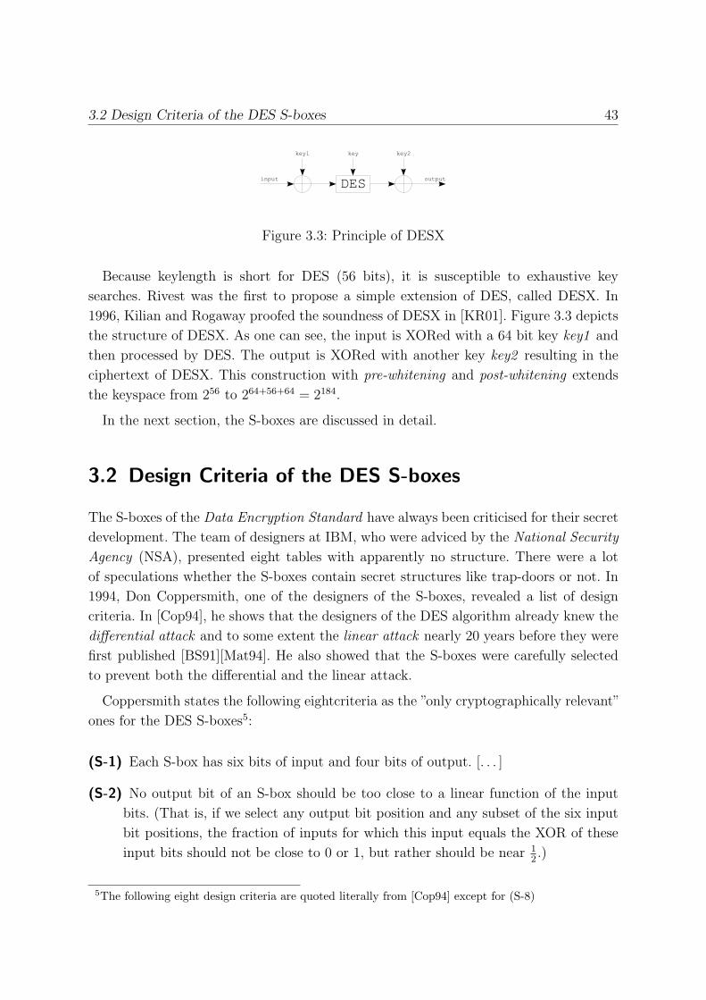
Figure 3.3: Principle of DESX
Because keylength is short for DES (56 bits), it is susceptible to exhaustive key
searches. Rivest was the first to propose a simple extension of DES, called DESX. In
1996, Kilian and Rogaway proofed the soundness of DESX in [KR01]. Figure 3.3 depicts
the structure of DESX. As one can see, the input is XORed with a 64 bit key key1 and
then processed by DES. The output is XORed with another key key2 resulting in the
ciphertext of DESX. This construction with pre-whitening and post-whitening extends
the keyspace from 256 to 264+56+64 = 2184.
In the next section, the S-boxes are discussed in detail.
3.2 Design Criteria of the DES S-boxes
The S-boxes of the Data Encryption Standard have always been criticised for their secret
development. The team of designers at IBM, who were adviced by the National Security
Agency (NSA), presented eight tables with apparently no structure. There were a lot
of speculations whether the S-boxes contain secret structures like trap-doors or not. In
1994, Don Coppersmith, one of the designers of the S-boxes, revealed a list of design
criteria. In [Cop94], he shows that the designers of the DES algorithm already knew the
differential attack and to some extent the linear attack nearly 20 years before they were
first published [BS91][Mat94]. He also showed that the S-boxes were carefully selected
to prevent both the differential and the linear attack.
Coppersmith states the following eightcriteria as the ”only cryptographically relevant”
ones for the DES S-boxes5:
(S-1) Each S-box has six bits of input and four bits of output. [. . . ]
(S-2) No output bit of an S-box should be too close to a linear function of the input
bits. (That is, if we select any output bit position and any subset of the six input
bit positions, the fraction of inputs for which this input equals the XOR of these
input bits should not be close to 0 or 1, but rather should be near 12.)
5The following eight design criteria are quoted literally from [Cop94] except for (S-8)

3.2 Design Criteria of the DES S-boxes 44
(S-3) If we fix the leftmost and rightmost input bits of the S-box and vary the four
middle bits, each possible 4-bit output is attained exactly once as the middle
input bits range over their 16 possibilities.
(S-4) If two inputs to an S-box differ in exactly one bit, the outputs must differ in at
least two bits.
(That is, if |∆Ii,j| = 1, then |∆Oi,j| ≥ 2, where |x| is the number of 1-bits in the
quantity x.)
(S-5) If two inputs to an S-box differ in the two middle bits exactly, the outputs must
differ in at least two bits.
(If ∆Ii,j = 001100, then |∆Oi,j| ≥ 2.)
(S-6) If two inputs to an S-box differ in their first two bits and are identical in their
last two bits, the two outputs must not be the same.
(If ∆Ii,j = 11xy00, where x and y are arbitrary bits, then ∆Oi,j 6= 0.)
(S-7) For any nonzero 6-bit-difference between inputs, ∆Ii,j, no more than eight of the
32 pairs of inputs exhibiting ∆Ii,j may result in the same output difference ∆Oi,j.
(S-8) Define
q0,j = maxc,d
prob(∆Oi,j = 0|∆Ii,j = 00cd11),
q1,j = maxg,h
prob(∆Oi,j = 0|∆Ii,j = 11gh10),
q2,j = maxk,m
prob(∆Oi,j = 0|∆Ii,j = 10km00).
dj = q0,jq1,j+1q2,j+2.
S-boxes must be arranged to minimize
maxj=1,2,...,8
dj.
In other words, the qi,j define the maximum number of input pairs, which cause a
collision for the specified input difference ∆Ii,j. For all possible combinations of S-box
triplets the maximum of dj should be minimised.
Subsequently, we give a short reasoning why these criteria are important. The DES al-
gorithm mainly consists of linear components like permutations, bitshiftings, and XORs.
Criterion (S-2) in particular ensures, that the entire algorithm is not linear, and thus can
be trivially broken. The maximum bias for all combinations of input bits for all S-boxes
is shown in Table 3.5.
Criterion (S-3) defines, that every row of an S-box is a permutation and accordingly
bijective. The avalanche effect is ensured by the criteria (S-4) and (S-5). To mount the

3.3 Improved Design Criteria 45
S-box i S7max ∆Ii,j ∆Oi,j
1 8 110100 000010
2 8 001000 001010
3 8 100000 001101
4 8 000001 000101
5 8 000101 001010
6 8 000001 001101
7 8 011000 000001
8 8 000001 000101
Table 3.2: Maximum values concerning criterion (S-7) of DES S-boxes
differential attack is complicated by criterion (S-7), because it reduces the probability
of collisions at the S-box output to 14
or less. Criterion (S-7) is already very strict, hence
we adopted it. As a matter of fact all DES S-boxes satisfy the criterion (S-7) exactly.
This is depicted in Table 3.2 together with an appropriate input difference.
The criteria (S-1) to (S-7) refer to one single S-box. The only criterion which deals
with the combinations of S-boxes is criterion (S-8). The designers goal was to minimize
the probability of collisions at the output of the S-boxes and thus at the output of the
f-function. As a matter of fact, it is only possible to cause a collision in three adjacent
S-boxes, but not in a single S-box or a pair of S-boxes due to the diffusion caused by
the expansion permutation. An attacker would like to find the input difference with the
highest probability of such collisions. Table 3.3 shows the values q0,j, q1,j, q2,j, and the
appropriate input differences for each of the eight DES S-boxes. The maximum proba-
bility for collisions of each S-box triplet together with the appropriate input difference
is shown in Table 3.4. As one can see, d3 is the smallest and d1 is the highest probability
for collisions in the DES S-boxes.
3.3 Improved Design Criteria
For the S-boxes of our lightweight design we tightened the constraints. We focused on
the criteria (S-2) and (S-6) because they are the most promising regarding linear and
differential cryptanalysis.
In the remainder of this section, we discuss criteria (S-2) and (S-6) and derive our
stronger design criteria (S-2”) and (S-6’).

3.3 Improved Design Criteria 46
S-boxes q0,j ∆Ii,j q1,j ∆Ii,j q2,j ∆Ii,j
1 0.218750 000011 0.093750 111010 0.187500 100100
2 0.093750 001011 0.125000 110010 0.156250 100100
3 0.125000 000011 0.125000 111110 0.156250 101100
4 0.125000 000011 0.250000 110010 0.250000 101000
5 0.125000 000011 0.062500 110010 0.125000 101100
6 0.093750 000111 0.125000 111010 0.156250 100100
7 0.125000 000011 0.250000 111010 0.218750 101000
8 0.125000 001111 0.125000 111010 0.156250 101000
Table 3.3: For criterion (S-8) maximum probabilities for collisions at single S-box outputs
Active S-boxes j dj ∆mj (hex)
1,2,3 0.004272 19600000
2,3,4 0.002930 05f40000
3,4,5 0.003906 00196000
4,5,6 0.001221 00019200
5,6,7 0.003418 00001d40
6,7,8 0.003662 000003d4
7,8,1 0.002930 2000001d
8,1,2 0.001831 d2000007
Table 3.4: Maximum probabilities dj of collisions in S-box triplets for 32-bit input dif-
ferentials ∆mj
3.3 Improved Design Criteria 47
3.3.1 Improved Criteria (S-2’) and (S-2”)
One possible step to improve the resistance of DES against linear cryptanalysis was
already proposed by Coppersmith. He defines a stronger criterion (S-2’) (difference to
(S-2) is printed bold) as follows:
(S-2’) No combination of output bits of an S-box should be too close to a linear
function of the input bits. (That is, if we select any subset of the four output
bit positions and any subset of the six input bits, the fraction of inputs for which
this input equals the XOR of these input bits should not be close to 0 or 1, but
rather should be near 12.)
All arbitrary combinations of input bits x and output bits S(x) can be linearly
approximated by the scalar products 〈a, x〉 and 〈b, S (x)〉, with a, x ∈ GF (2)6 and
b, S (x) ∈ GF (2)4, respectively. Let Sb = 〈b, S (x)〉 denote a combination of output bits,
that is determined by b. Then, the Walsh-coefficient Swb (a) is a measure for the linear
approximation of the output combination Sb by an input combination, that is determined
by a.
Swb (a) = # {x|Sb (x) = 〈a, x〉} −# {x|Sb (x) 6= 〈a, x〉} = 2# {x|Sb (x) = 〈a, x〉} − 26
(3.2)
The probability of a linear approximation of a combination of output bits Sb by a
combination of input bits, that is determined by a, in round i can be written as:
pi =# {x|Sb (x) = 〈a, x〉}
26(3.3)
Combining equations 3.2 and 3.3 leads to:
pi =Sw
b (a)
27+
1
2(3.4)
The linear probability bias ε is a correlation measure for this deviation from probability12
for which it is entirely uncorrelated. It is
ε =
∣∣∣∣pi − 1
2
∣∣∣∣ =
∣∣∣∣Sw
b (a)
27
∣∣∣∣ (3.5)
Let us denote the maximum value derived from the Walsh-Transformation by S2max.
Then:
ε =
∣∣∣∣S2max (a)
27
∣∣∣∣ (3.6)
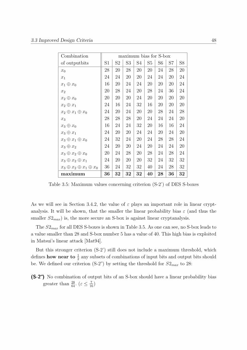
3.3 Improved Design Criteria 48
Combination maximum bias for S-box
of outputbits S1 S2 S3 S4 S5 S6 S7 S8
x0 28 20 28 20 20 24 28 20
x1 24 24 20 20 24 24 20 24
x1 ⊕ x0 16 20 24 24 20 20 20 24
x2 20 28 24 20 28 24 36 24
x2 ⊕ x0 20 20 20 24 20 20 20 20
x2 ⊕ x1 24 16 24 32 16 20 20 20
x2 ⊕ x1 ⊕ x0 24 20 24 20 20 28 24 28
x3 28 28 28 20 24 24 24 20
x3 ⊕ x0 16 24 24 32 20 16 16 24
x3 ⊕ x1 24 20 20 24 24 20 24 20
x3 ⊕ x1 ⊕ x0 24 32 24 20 24 28 28 24
x3 ⊕ x2 24 20 20 24 20 24 24 20
x3 ⊕ x2 ⊕ x0 20 24 28 20 28 24 28 24
x3 ⊕ x2 ⊕ x1 24 20 20 20 32 24 32 32
x3 ⊕ x2 ⊕ x1 ⊕ x0 36 24 32 32 40 24 28 32
maximum 36 32 32 32 40 28 36 32
Table 3.5: Maximum values concerning criterion (S-2’) of DES S-boxes
As we will see in Section 3.4.2, the value of ε plays an important role in linear crypt-
analysis. It will be shown, that the smaller the linear probability bias ε (and thus the
smaller S2max) is, the more secure an S-box is against linear cryptanalysis.
The S2max for all DES S-boxes is shown in Table 3.5. As one can see, no S-box leads to
a value smaller than 28 and S-box number 5 has a value of 40. This high bias is exploited
in Matsui’s linear attack [Mat94].
But this stronger criterion (S-2’) still does not include a maximum threshold, which
defines how near to 12
any subsets of combinations of input bits and output bits should
be. We defined our criterion (S-2”) by setting the threshold for S2max to 28:
(S-2”) No combination of output bits of an S-box should have a linear probability bias
greater than 2864
. (ε ≤ 716
)

3.3 Improved Design Criteria 49
3.3.2 Improved Criterion (S-6’)
Better than minimising the probability for collisions in three or more adjacent S-boxes,
is to eliminate them. Consider an input difference ∆Ii,j of the an S-box i which results
in an output difference ∆Oi,j = 0:
∆Ii,j = abcdef,
where a, b, c, d, e, f are arbitrary bits. If S-box i is the rightmost active S-box of an S-box
tuple and there are seven or less active S-boxes, then input bits e and f have to be 0.
∆Ii,j = abcd00
Design criterion (S-4) states, that there are no collisions in one row of an S-box, hence
a has to be 1.
∆Ii,j = 1bcd00
This is always the input difference of the rightmost active S-box for any number of
adjacent S-boxes except for eight adjacent active S-boxes. If there are no collisions with
such kind of input differences, differential attacks using differentials like the one presented
by Biham and Shamir in [BS92], will not work any longer. Hence, we can replace (S-6)
and (S-8’) by our improved design criterion (S-6’):
(S-6’) If two inputs to an S-box differ in their first bit and are identical in their last
two bits, the two outputs must not be the same.
(If ∆Ii,j = 1xyz00, where x,y and z are arbitrary bits, then ∆Oi,j 6= 0.)
Note that the pattern ∆Ii,j = 11xy00 used to define q2,j in (S-8) is a special case of the
input difference ∆Ii,j = 1xyz00 used in (S-6’). Hence, dj always will be zero.
3.3.3 Improved S-box
In Section 3.3, we derived stronger requirements for an S-box. We randomly generated
S-boxes, which fulfill the original DES criteria (S-1), (S-3), (S-4), (S-5), (S-7), and the
newly defined criteria (S-2”) and (S-6’). Our goal was to find one single S-box, which
is significantly more resistant against differential and linear cryptanalysis. In our DLX
algorithm this S-box will replace all eight S-boxes in DES. This approach gives rise to a
greatly decreased demand for chip size (see Section 3.6.2).
We chose an S-box which achieves a maximum linear bias of 28 (S-2”) and a maximum
occurrence of 7 for a fixed input and output difference (S-7). Table 3.6 shows the best
S-box we found in 1000 S-boxes, that fulfill all criteria. During the search, more than
200 million S-boxes were discarded.

3.4 DLX - A Modified Lightweight DESX Variant 50
S
14 9 5 6 2 12 11 0 7 4 8 15 13 3 1 10
8 14 11 13 5 0 6 3 1 2 7 4 10 15 12 9
9 2 3 8 15 5 4 11 12 7 6 1 0 14 10 13
4 7 14 1 2 11 13 8 15 12 0 10 9 5 3 6
Table 3.6: Improved DLX S-box
3.4 DLX - A Modified Lightweight DESX Variant
In this section our new DLX algorithm is presented. DLX stands for DES Lightweight
eXtension. Similar to DESX, it uses key whitening at the input and output of the
block cipher. First we give a description of the algorithm, where the modifications in
comparison to DESX are presented. Subsequently, the cryptographic properties of DLX
are discussed.
3.4.1 Description of DLX
We wanted to build an encryption engine suitable for RFIDs, hence we substituted time
by chip size wherever possible. With our DESX ASIC design registers take up the main
part of chip size (29.67%), followed by the S-boxes (28.2%), multiplexors (27.4%) and
XORs (13.1%)6. chip size of registers, multiplexors and XORS can not be optimised any
further, hence we thought about possibilities to optimize the chip size of the S-boxes.
The only difference between DLX and DESX or DES, respectively, lies in the f -
function. We substituted the eight original DES S-boxes by a single but stronger S-box,
which is repeated eight times. There have been other approaches to alter the S-boxes, like
key-dependent S-boxes [BB94][BS92] or the so-called siDES [KLPL94][KLPL95][KPL].
But all these approaches, despite the fact that some of them have worse properties than
DES [Knu], just change the content and not the number of S-boxes. To the best of our
knowledge, no one has ever discussed a DES variant with just one S-box, repeated eight
times.
The structure of the f -function of our modified DES is depicted in Figure 3.4.
692.9% of the XOR chip size is used by pre- and postwhitening due to DESX.
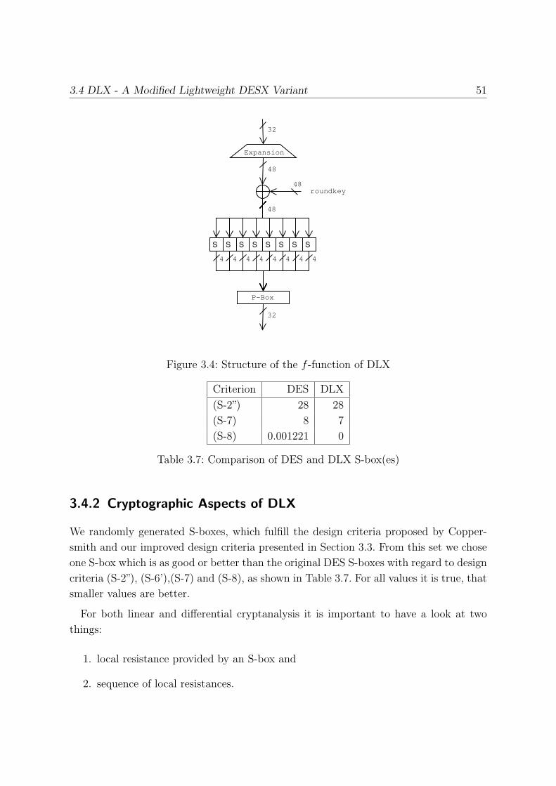
3.4 DLX - A Modified Lightweight DESX Variant 51
Expansion
48
48
32
S S S S S S S S
roundkey
48
P-Box
32
4 4 4 4 4 4 4 4
Figure 3.4: Structure of the f -function of DLX
Criterion DES DLX
(S-2”) 28 28
(S-7) 8 7
(S-8) 0.001221 0
Table 3.7: Comparison of DES and DLX S-box(es)
3.4.2 Cryptographic Aspects of DLX
We randomly generated S-boxes, which fulfill the design criteria proposed by Copper-
smith and our improved design criteria presented in Section 3.3. From this set we chose
one S-box which is as good or better than the original DES S-boxes with regard to design
criteria (S-2”), (S-6’),(S-7) and (S-8), as shown in Table 3.7. For all values it is true, that
smaller values are better.
For both linear and differential cryptanalysis it is important to have a look at two
things:
1. local resistance provided by an S-box and
2. sequence of local resistances.

3.4 DLX - A Modified Lightweight DESX Variant 52
Local resistance provided by an S-box against linear cryptanalysis is given by the maxi-
mum bias or maximum linear correlation, determined by the (S-2”) value. For differential
cryptanalysis local resistance is given by a low differential probability, determined by the
(S-7) value. After looking at the local resistance, one should have a look at the sequence
of local resistances. It is important to prevent that a sequence of local resistances can be
concatenated together to attack the whole cipher.
In the remainder of this section we discuss differential as well as linear cryptanalysis
and show that DLX is more resistant to both attacks than DES.
Differential Cryptanalysis
This attack was first presented by Biham and Shamir [BS91] in 1990. An attacker starts
with two messages m and m’, which differ by a known XOR differential ∆m. Let ∆mi =
mi ⊕ m′i denote the difference between intermediate message halves. The input to the
f -function is always given by: E (mi ⊕ ki)j or E (m′i ⊕ ki)j, respectively. The XOR of
these two inputs leads to: (E (mi ⊕ ki))j ⊕ (E (m′i ⊕ ki))j = E (mi ⊕m′
i)j = E (∆mi)j.
As one can see, the input difference of an S-box does not depend anymore on round
key ki. Following Coppersmith we denote the input difference of round i in S-box j as
∆Ii,j ∈ GF (2)6 and the XOR sum of the corresponding outputs as ∆Oi,j ∈ GF (2)4. If
the input difference ∆Ii,j is fixed, one can compute the output differences ∆Oi,j for all
32 pairs of inputs, which provide the given input difference ∆Ii,j. The number of equal
output differences is a criterion for differential cryptanalysis: the higher the number of
occurrences of an output difference ∆Oi,j, the higher the probability, that for a given
input difference ∆Ii,j this output difference will occur. Hence, an attacker can guess the
output difference for any input difference ∆Ii,j with probability p (∆Oi,j = 0|∆Ii,j). The
maximum probability is a benchmark for the local resistance provided by this S-box,
where a high probability means bad resistance.
Let us define a characteristic Γ as follows:
Γ := (∆m,λ, ∆c)
∆m = m⊕m′
∆c = c⊕ c′
λ = (λ1, . . . , λn) , λi = (∆xi, ∆yi)
where ∆xi denotes the input difference of the f -function in round i, ∆yi denotes the
output difference of the f -function in round i, n denotes the number of rounds, ∆m

3.4 DLX - A Modified Lightweight DESX Variant 53
denotes the input difference and ∆c the output difference of the whole 16 rounds DES.
For DES the following equations hold true:
∆x1 = ∆mr
∆x2 = ∆ml ⊕∆y1
∆yn = ∆cl ⊕∆xn−1
∆yi = ∆xi−1 ⊕∆xi+1, 2 ≤ i ≤ n− 1
The probability that the n-round characteristic pΓ holds true, is defined as the product
of the probabilities pi of output collisions for each round i:
pΓ =n∏
i=1
pi =n∏
i=1
p (∆xi∆yi|F )
This probability is based on the assumption that the round keys are statistically inde-
pendent. As a matter of fact, the round keys of DES are deduced in a linear fashion and,
thus, they are statistically dependent.
To derive keybits an attacker has to perform the following steps:
1. generate chosen plaintexts m and m′ with m⊕m′ = ∆m.
2. encrypt m and m′ with DES and determine ∆c = c⊕ c′, where c = DES (m) and
c′ = DES (m′).
3. always check which keys can lead to input difference ∆xn in round n.
In step three, some keys can always create the required input difference, they are
called candidates. If the characteristic holds true, the right key must be included in the
set of key candidates. If the characteristic is wrong, random keys are added to the set of
candidates. Let M denote pairs of chosen plaintexts with input difference ∆m and let α
denote candidates for the key. Because the characteristic Γ holds true with probability
pΓ, the right key must be approximately MpΓ times included in the set of key candidates.
If M is big enough, the right key is significantly more often included in the set of key
candidates, because it is reasonable to assume that any other key candidate is randomly
added.
The Feistel -structure of DES can be used to extend weak local resistance to a sequence
of weak local resistances, a so called characteristic. Most promising for differential crypt-
analysis are three adjacent active S-boxes in round i and no active S-box in round i+1,

3.4 DLX - A Modified Lightweight DESX Variant 54
because these characteristics can be concatenated to two-rounds characteristic, as de-
picted in Figure 3.5. The input difference propagates through all 16 rounds of DES,
resulting in a differential path.
Consider the following input differences for the three adjacent active S-boxes j,j+1
and j+2 in round i:
∆Ii,j = abcdef
∆Ii,j+1 = efghij
∆Ii,j+3 = ijkmnp
with a, b, c, d, e, f, g, h, i, j, k, m, n, p ∈ 0, 1. Because all other S-boxes are passive the
input bits a,b,n and p have to be 0. Hence we have
∆Ii,j = 00cdef
∆Ii,j+1 = efghij
∆Ii,j+2 = ijkm00
Because design criterion (S-3) states, that each row of any S-box is a permutation, and
hence can not cause a collision, the input bits f and i have to be 1. Thus we get
∆Ii,j = 00cde1
∆Ii,j+1 = e1gh1j
∆Ii,j+2 = 1jkm00
Considering design criterion (S-6), which states, that any input difference ∆Ii,j = 11xy00
can not cause a collision, it is obvious that j has to be zero and thus we get
∆Ii,j = 00cde1
∆Ii,j+1 = e1gh10
∆Ii,j+2 = 10km00
From design criterion (S-4) it is possible to derive another bit for ∆Ii,j+1. Because each
row has to be a permutation, input bit e has to be 1, resulting in:
∆Ii,j = 00cd11
∆Ii,j+1 = 11gh10
∆Ii,j+2 = 10km00

3.4 DLX - A Modified Lightweight DESX Variant 55
The example depicted in Figure 3.5 uses the pattern of [BS92]:
∆Ii,1 = 000011
∆Ii,2 = 110010
∆Ii,3 = 101100
∆Ii,j = 000000, j = 4, 5, 6, 7, 8
Before expansion the input differences are (in hexadecimal notation):
∆Ii,1 = 0001 = 1(hex)
∆Ii,2 = 1001 = 9(hex)
∆Ii,3 = 0110 = 6(hex)
As one can see in this example, for the input difference
∆Ii = (∆Ii,1∆Ii,2∆Ii,3∆Ii,4∆Ii,5∆Ii,6∆Ii,7∆Ii,8) = 19600000
in round i there are collisions in three adjacent S-boxes, resulting in an output difference
of
∆Oi = 00000000.
The right half, denoted by ∆Ri, is always stored as the new left half, denoted by ∆Li+1,
hence ∆Li+1 = ∆Ri = ∆Ii. The left half (∆Li) is XORed with the output of the f -
function (∆Oi) and stored as the new right half (∆Ri+1), thus ∆Ri+1 = ∆Oi ⊕∆Li =
∆Li. In round i+1 the - nonexistent - input difference ∆Ii+1 = 00000000(hex) of course
leads to an output difference of ∆Oi+1 = 00000000 (hex). The fact, that ∆Li+1 = ∆Ii =
19600000 is XORed with ∆Oi+1 = 0000000 leads to the result, that ∆Ri+2 = ∆Li+1 =
∆Ii = 19600000 and hence, more important, that ∆Ii+2 = ∆Ii. This can be extended
for more than two rounds, resulting in a characteristic for all 16 rounds of DES.
Every wrong key candidate is included in roughly Mα256 sets of key candidates. A measure
for the success of a differential attack is defined by the Signal-to-Noise-Ratio
S
N:=
MpΓ
Mα256
=pΓ
α256.
If the Signal-to-Noise-Ratio is too small, it may happen that the right key cannot be
spotted inside the set of candidates. Thus, the higher the Signal-to-Noise-Ratio the easier
the attack.

3.4 DLX - A Modified Lightweight DESX Variant 56
As a rule-of-thumb for the number of needed chosen plaintexts M , [How] states
M ≈ c
pΓ,
where c is a small constant. We can conclude, that a smaller probability pΓ increases the
amount of needed chosen plaintexts M .
To thwart such attacks, the team of designers at IBM implemented two countermea-
sures. With design criterion (S-7) the probability of a characteristic got an upper bound.
Furthermore they increased the number of active S-boxes by design criteria for the per-
mutations.
The probability for the most successfull characteristic is determined by the probability
of a collision in three adjacent S-boxes. Since this value is bounded by the (S-8) crite-
rion, the probability of a successful differential attack is the product of all sequential
probabilities.
Coppersmith showed in [Cop94], that it is impossible to create collisions if only one or
two adjacent S-boxes are active. Furthermore, in our DLX algorithm, the probability for
a collision in three, four, five, six, or seven adjacent S-boxes is 0, as indicated by criterion
(S-6’). Hence, if an attacker wants to combine a two-round characteristic, he needs to
create a collision in at least eight adjacent S-boxes. The probability p (∆Oi,j = 0|∆Ii,j)
is bounded by the design criterion (S-7) to:
p (∆Oi,j = 0|∆Ii,j) ≤ S7max
32=
7
32As one can see from Table 3.7 our S-box has a maximum of seven out of 32 input
differences, that can create collisions, hence the probability pi for collisions in eight
adjacent S-boxes is
pi =
(7
32
)8
.
Together with the fact, that one has to iterate this six times, we have an upper bound
of
p =6∏
i=1
pi =
(7
32
)48
resulting in at least 2105 chosen plaintexts. Hence, a differential attack using the best
characteristics is not possible anymore.
Linear Cryptanalysis
Linear cryptanalysis, first published in 1993 by Matsui [Mat94], uses linear approxima-
tion to describe the encryption algorithm. It is the most efficient attack on DES with
approximately 243 needed known plaintexts.

3.4 DLX - A Modified Lightweight DESX Variant 57
Figure 3.5: 2 round characteristic in DES
3.5 A size-optimised VHDL Design of DESX and DLX 58
For all combinations of S-box output bits an attacker calculates the Walsh-coefficients
of all combinations of S-box input bits. If the S-box were completely immune against
linear attacks, the input and output bits of the S-boxes would be uncorrelated and all
Walsh-coefficients would be 0, instead of ranging from −26 to 26. A Walsh-coefficient of
26 means that this combination of output bits is always the XOR sum of the appropriate
combination of input bits, hence it is linear. If a combination of output bits has a Walsh-
coefficient of −26, this combination is affine. In the last row of Table 3.5, the absolute
values of the Walsh-coefficients for all DES S-boxes are shown.
As introduced in Section 3.3, ε is a correlation measurement for the deviation from
probability 12:
ε =
∣∣∣∣pi − 1
2
∣∣∣∣ ,
where pi = S2max
27 describes the probability of a linear approximation, based on the
Walsh-coefficient. From the well-known pilling-up lemma [Sti02] we derive the following
equation for the n-rounds bias ε(n) :
ε(n) = 2n−1
n∏i=1
∣∣∣∣pi − 1
2
∣∣∣∣ = 2n−1
n∏i=1
∣∣∣∣S2max
27
∣∣∣∣ (3.7)
According to [Mat94], the amount (m) of needed plaintexts for the linear attack is :
m ≈ c
ε2(n)
,
where c is a small constant. As one can see, the amount of plaintext increases with
quadratic complexity with smaller bias ε(n) and hence with smaller S2max. Matsui ex-
ploited the high bias of S-box 5 (40) and S-box 1 (36). Our chosen S-box has a S2max
value of 28, which is much smaller than these values. This leads to an attacker needing
about 90000 times more plaintexts for successfully performing a linear attack on DLX
compared to DES.
3.5 A size-optimised VHDL Design of DESX and DLX
In this section a size-optimised VHDL design of the DESX algorithm is presented. The
goal was to design an encryption engine, which can be used in an RFID tag for authen-
tication. Hence, this design is suitable only for encryption but not for decryption.
The remainder of this section is organised as follows: first, the modules are treated,
and second, the datapath is discussed.

3.5 A size-optimised VHDL Design of DESX and DLX 59
3.5.1 The Modules
The overall architecture of the ASIC is depicted in Figure 3.6. It has the following input
and output signals:
� Input signals
clk clocks the chip
n reset resets the chip. This flag is active low.
input is a 64-bit wide input bus. This data will be processed by the ASIC as
plaintext to be encrypted.
key is a 56-bit wide input bus. This key is used in the DES cipher for encryption.
key1 is a 64-bit wide input bus. This key is used for pre-whitening.
key2 is a 64-bit wide input bus. This key is used for post-whitening.
� Output signals
output is a 64-bit wide output bus. The result of the encryption will be sent to
this bus.
done is a flag, that shows if the output is valid or not.
entity desx i sport (
c l k : in s t d l o g i c ;n r e s e t : in s t d l o g i c ;input : in s t d l o g i c v e c t o r (63 downto 0 ) ;key : in s t d l o g i c v e c t o r (55 downto 0 ) ;key1 : in s t d l o g i c v e c t o r (63 downto 0 ) ;key2 : in s t d l o g i c v e c t o r (63 downto 0 ) ;output : out s t d l o g i c v e c t o r (63 downto 0 ) ;done : out s t d l o g i c) ;
end entity desx ;
Our design is composed of five modules: mem left, mem right, keyschedule, controller,
and sbox. A description of these modules is given in the subsequent sections.

3.5 A size-optimised VHDL Design of DESX and DLX 60
Sbox
Mem-
left
Key-
schedule
Mem-
right
Con-
troller
CLK
n_reset
input[64]
key[56]
key1[64]
key2[64]
output[64]
done
Figure 3.6: Input and Output of the DESX ASIC
controller
The controller module manages all control signals in the ASIC based on the finite state
machine depicted in Figure 3.7. After the ASIC is reset by the active-low n reset signal,
it transits to the IDLE state. In this state counters are reset and flip-flops are loaded
with initial inputs. One cycle later it transits to the ROUND state, where it stays
for another eight cycles. During this period, the 4-bit output of the eight flip-flops in
module mem right are processed consecutively. The right part of the round key and the
appropriate S-box are selected by the count signal. If the s counter signal equals eight, it
transits to the INIT ROUND state. During this state, the content of mem left flip-flop
and mem right flip-flop is swapped in one cycle. In round 2, 9, and 16, the key is rotated
by one instead of two bits, which is controlled by the ctrl key signal during this state.
One cycle later it transits back to the ROUND state. This repeats another 15 times
until the count rounds signal equals 16. Now, all 16 rounds of DES have been processed
and the ASIC transits to the DONE state, where the done output flag signals a valid
output. One cycle later, it is again in the IDLE state.
Below is a list of the input and output signals of the controller entity:
entity c o n t r o l l e r i sport (
c l k : in s t d l o g i c ;n r e s e t : in s t d l o g i c ;c t r l k e y f f : out s t d l o g i c v e c t o r ( 1 downto 0 ) ;c t r l i n i t : out s t d l o g i c v e c t o r ( 1 downto 0 ) ;count : out s t d l o g i c v e c t o r ( 2 downto 0 ) ;c t r l d on e : out s t d l o g i c) ;
end entity c o n t r o l l e r ;

3.5 A size-optimised VHDL Design of DESX and DLX 61
Figure 3.7: Finite State Machine of the DESX ASIC
keyschedule
In this module all round keys are generated. It is composed of a 56-bit register, an input
multiplexor, and an output multiplexor. The input multiplexor of the key flip-flop is
controlled by the 2-bit wide ctrl keyff signal. It allows to select input between initial
key and the current value of the key flip-flop. The current value is either saved without
modification, or applied to the leftshift permutation of DES once (LS) or twice (LS2).
The output multiplexor is controlled by the 3-bit wide count signal. All permutations
like permuted choice 1 (PC1), permuted choice 2 (PC2), leftshift by one bit (LS), and
leftshift by two bits (LS2) can be implemented by wiring. Input signals for this module
are the 56-bit wide key input bus, 2-bit wide ctrl keyff, and 3-bit wide count control
signals. Output signal is 6-bit wide round key output bus. The following VHDL code
fragment lists all input and output signals of the Keyschedule module:
entity keyschedule i sport (
c l k : in s t d l o g i c ;key : in s t d l o g i c v e c t o r (55 downto 0 ) ;c t r l k e y f f : in s t d l o g i c v e c t o r ( 1 downto 0 ) ;count : in s t d l o g i c v e c t o r ( 2 downto 0 ) ;key out : out s t d l o g i c v e c t o r ( 5 downto 0 )) ;
end entity keyschedule ;

3.5 A size-optimised VHDL Design of DESX and DLX 62
mem left
This module consists of eight 4-bit wide registers, each composed of D-flip-flops. Input
signals are 2-bit wide ctrl init control signal, 4-bit wide input bus in p, 32-bit wide input
bus in right, and 32-bit wide input bus in ip. Output signals are 4-bit wide output bus
out p and 32-bit wide output bus out right.
entity mem left i sport (
c l k : in s t d l o g i c ;i n i p : in s t d l o g i c v e c t o r (31 downto 0 ) ;i n r i g h t : in s t d l o g i c v e c t o r (31 downto 0 ) ;in p : in s t d l o g i c v e c t o r ( 3 downto 0 ) ;c t r l i n i t : in s t d l o g i c v e c t o r ( 1 downto 0 ) ;ou t r i gh t : out s t d l o g i c v e c t o r (31 downto 0 ) ;out p : out s t d l o g i c v e c t o r ( 3 downto 0 )) ;
end entity mem left ;
When the ASIC is in ROUND state, outputs of the flip-flops are clocked into the
succeeding flip-flops. The output of the last flip-flop is XORed with the output of the
sbox module and stored in the first flip-flop. When the ASIC is in INIT ROUND state,
the 32-bit wide input in right is split into eight times 4-bit and stored in the flip-flops.
The 32-bit wide output bus out right is composed of the 4-bit wide outputs of all eight
flip-flops.
mem right
This module is similar to the the mem left module with slight differences. It also consists
of eight 4-bit wide registers, but it has different input and output signals, as shown in
the following VHDL code fragment.
entity mem right i sport (
c l k : in s t d l o g i c ;i n i p : in s t d l o g i c v e c t o r (31 downto 0 ) ;i n l e f t : in s t d l o g i c v e c t o r (31 downto 0 ) ;c t r l i n i t : in s t d l o g i c v e c t o r ( 1 downto 0 ) ;o u t l e f t : out s t d l o g i c v e c t o r (31 downto 0 ) ;out sbox : out s t d l o g i c v e c t o r ( 5 downto 0 )) ;
end entity mem right ;

3.5 A size-optimised VHDL Design of DESX and DLX 63
When the ASIC is in ROUND state, outputs of the flip-flops are clocked into the
succeeding flip-flops. The output of the last flip-flop is stored in the first flip-flop. When
the ASIC is in INIT ROUND state, the 32-bit wide input in right is split into eight
times 4-bit and stored in the flip-flops. The 6-bit wide output bus out sbox is composed
of the output of the last flip-flop, the most-significant bit of its predecessor flip-flop
and the least-significant it of the first flip-flop. Hence, the expansion function of DES
is implemented by wiring. This is depicted by the light-gray box, labeled with E, in
Figure 3.8 The 32-bit wide output bus out left is composed of the 4-bit wide outputs of
all eight flip-flops.
sbox
This module consists of eight S-boxes of the DES algorithm and an output multiplexor.
Input signals are a 6-bit wide input bus sbox in and a 3-bit wide control signal count. A
4-bit wide output bus sbox out forwards the selected S-box output.
The S-boxes are realised in combinatorial logic.
entity sbox i sport (
sbox in : in s t d l o g i c v e c t o r ( 5 downto 0 ) ;count : in s t d l o g i c v e c t o r ( 2 downto 0 ) ;sbox out : out s t d l o g i c v e c t o r ( 3 downto 0 )) ;
end entity sbox ;
3.5.2 The Datapath
Figure 3.8 shows the datapath of our DESX design. As one can see, the key is stored
in the key flip-flop after the permuted choice 1 and a left shift by one bit is applied.
Initially, the input is XORed with the key1 for pre-whitening. Afterwards the Initial
Permutation (IP) is applied, and the data is split into two 32-bit wide inputs for the
modules mem left and mem right, respectively. The input of mem left is modified by the
inverse of the P permutation (P−1). Since the P permutation and its inverse are linear
functions, the following equation holds true:
P(P−1 (x)
)= x
We will discuss this modification later in this section. Both 32-bit input blocks are each
split into eight 4-bit fractions. They are stored in the registers of the modules mem left

3.5 A size-optimised VHDL Design of DESX and DLX 64
and mem right in one cycle. Now, the output of the last register in mem right is both
stored in the first register of mem right and expanded to six bits. After an XOR operation
with the appropriate fraction of the round key, this expanded value is processed by the
sbox module. Here it is substituted by all eight DES S-boxes. The count signal selects
the right value, which is, after an XOR operation with the last output of the mem left
module, stored in the first flip-flop of the mem left module. This is repeated eight times,
until all 32 bit of the right half are processed.
Due to the fact, that we wanted to develop a design, which is extremely size-optimised,
we always substituted chip size by time. Therefore, we chose a 4-bit wide datapath
instead of a 32-bit wide datapath. In DES, the P permutation is applied in the f -
function after the S-box substitution, as depicted in Figure 3.1. Afterwards the left half
is XORed and stored as the new right half. The P permutation of DES has an impact
on all 32 bits, hence it has to be processed at once. In our design, we applied the P
permutation in each ninth round. Because the P−1 permutation was applied before the
left half was stored in the mem left module, we implemented the following:
P(P−1 (Li)⊕ S (E (Ri)⊕ keyi)
),
where Li denotes the left half, Ri denotes the right half, and keyi denotes the round
key. Because in DES all permutations are linear, the equation can be transformed to:⇒ P (P−1 (Li)⊕ S (E (Ri)⊕ keyi))
⇒ P (P−1 (Li))⊕ P (S (E (Ri)⊕ keyi))
⇒ Li ⊕ S (E (Ri)⊕ keyi)
Obviously, this is one round of DES. Table 3.8 shows the P function and its inverse
P−1.
Table 3.9 shows the number of needed transistors for some standard gates. As one can
see, for a 1-bit XOR operation 10 transistors are needed and for a 2-to-1-multiplexor
with a 1-bit wide input, 12 transistors are needed.
Hence, by reducing the datapath from 32-bit to 4-bit, only 6 ∗ 10 + 4 ∗ 10 = 100
transistors are needed, compared to 48∗10+32∗10 = 800 transistors. This saving comes
with the disadvantage of two additional multiplexors, each one for the round key (288
transistors) and for the S-box output (192 transistors). As we will show in Section 3.6.2,
the multiplexor for the S-box output is not necessary in our DLX algorithm.
When all eight fractions of both halves are processed, they are concatenated to two
32-bit wide outputs of the modules mem left and mem right. The output of the module
mem left is transformed by the P permutation and stored as the new content of the
mem right module, while the output of the mem right module is stored as the new
content of the mem left module.

3.6 Implementations of DESX and DLX 65
(a) P function
P
16 7 20 21
29 12 28 17
1 15 23 26
5 18 31 10
2 8 24 14
32 27 3 9
19 13 30 6
22 11 4 25
(b) P−1 function
P−1
9 17 23 31
13 28 2 18
24 16 30 6
26 20 10 1
8 14 25 3
4 29 11 19
32 12 22 7
5 27 15 21
Table 3.8: P function and P−1 function of DES
Gate Transistors
1-bit-XOR 10
2-to-1-MUX 12
Table 3.9: Number of transistors necessary for some standard gates
This procedure is repeated another 15 times. Then, both outputs of the memory
modules mem left and mem right are concatenated to a 64-bit wide data word. This
data word is processed by the Inverse Initial Permutation (IP−1) before the key2 is
XORed for post-whitening. The result is a valid ciphertext of the DESX algorithm.
3.5.3 VHDL Design of DLX
The design of our DLX algorithm is exactly the same as for the DESX algorithm, except
for the sbox module. We changed it to a module, which implements only one S-box. As
one can see in Figure 3.9, this module does not need the count control signal nor an
output multiplexor, which saves another 192 transistors.
3.6 Implementations of DESX and DLX
In this section the implementation results of DESX and DLX are presented.

3.6 Implementations of DESX and DLX 66
Figure 3.8: Datapath of the DESX
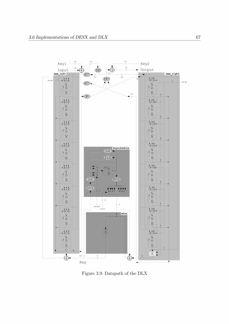
3.6 Implementations of DESX and DLX 67
Figure 3.9: Datapath of the DLX

3.6 Implementations of DESX and DLX 68
(a) Size
setup cycles 1
# clock cycles 144
# transistors 10516
area 0.049697mm2
(b) Power consumption and throughput at 100
kHz and 500 kHz
frequency 100 kHz 500 kHz
peak power [mA] 23.431 23.429
average power [µA] 1.1868 5.9466
[µW] 2.136 10.7
RMS power [µA] 92.678 207.53
[µW] 166.84 373.53
throughput [KB/s] 5.55 27.77
Table 3.10: Results of DESX, built in 0.18 µm CMOS
3.6.1 Implementation of DESX
We synthesized the VHDL design presented in Section 3.5 with the design flow described
in Section 2.6.1. Again, we used Synopsys Design Vision V-2004.06-SP2 to map our
DESX design to the Artisan UMC 0.18µm L180 Process 1.8-Volt Sage-X Standard Cell
Library and Cadence Silicon Ensemble 5.4 for the Placement & Routing-step.
As one can see from the following report, the complete layout after the Placement &
Routing - step consists of 1718 standard cells arranged in 35 rows.********************SILICON ENSEMBLE DESIGN SUMMARY REPORT********************Time : 1 7 : 4 1 : 2 0 , 2 5 October 2005
Design name : desx
Report f i l e name : PAR/RPT/OR des . summary
page 8
** UTILIZATION OF ALL ROW TYPES
Type Number Length Area % Row Space
umc6site Rows 35 6167700 31085208000
umc6site Ce l l s 1718 6167700 31085208000 100.00
Area of chip : 49697524800 ( square DBU)
Area requ i r ed for a l l c e l l s : 31085208000 ( square DBU)
Area u t i l i z a t i o n of a l l c e l l s : 62 .55%
********************SILICON ENSEMBLE DESIGN SUMMARY REPORT********************
The ASIC has a total area of 49697µm2 and an area utilization of 62.55%. It takes 144
clock cycles to encrypt one 64-bit block of plaintext. For one encryption at 100 kHz the
average power consumption is 1.1868 µA, at 500 kHz it is 5.9466 µA. The throughput
reaches 5.55 KB/s at 100 kHz and 27.78 KB/s at 500 kHz. All results are summarised
in Table 3.6.1. The layout of the DESX ASIC is depicted in Figure 3.10.

3.6 Implementations of DESX and DLX 69
Figure 3.10: Layout of the DESX ASIC
3.6.2 Implementation of DLX
In this section the results of the synthesised DLX are presented. As one can see from
the following report, the complete layout after the Placement & Routing - step consists
of 1312 standard cells arranged in 31 rows.********************SILICON ENSEMBLE DESIGN SUMMARY REPORT********************Time : 1 : 1 9 : 0 0 , 2 9 November 2005
Design name : dlx
Report f i l e name : PAR/RPT/OR dlx . summary
page 6
** UTILIZATION OF ALL ROW TYPES
Type Number Length Area % Row Space
umc6site Rows 31 4971780 25057771200
umc6site Ce l l s 1312 4971780 25057771200 100.00
Area of chip : 42919060800 ( square DBU)
Area requ i r ed for a l l c e l l s : 25057771200 ( square DBU)
Area u t i l i z a t i o n of a l l c e l l s : 58 .38%
********************SILICON ENSEMBLE DESIGN SUMMARY REPORT********************
The ASIC has a total area of 42919µm2 and an area utilization of 58.38%. It takes 144
clock cycles to encrypt one 64-bit block of plaintext. For one encryption at 100 kHz the
average power consumption is 0.89 µA, at 500 kHz it is 4.4477 µA. The throughput
reaches 5.55 KB/s at 100 kHz and 27.78 KB/s at 500 kHz. All results are summarised
in Table 3.6.2. The layout of the DLX ASIC is depicted in Figure 3.11.

3.6 Implementations of DESX and DLX 70
(a) Size
setup cycles 1
# clock cycles 144
# transistors 8672
area 0.042919mm2
(b) Power consumption and throughput at 100
kHz and 500 kHz
frequency 100 kHz 500 kHz
peak power [mA] 24.633 24.019
average power [µA] 0.89 4.4477
[µW] 1.604 8.0
RMS power [µA] 79.579 177.87
[µW] 143.24 320.15
throughput [KB/s] 5.55 27.77
Table 3.11: Results of DLX, built in 0.18 µm CMOS
Figure 3.11: Layout of the DLX ASIC

3.7 DESX versus DLX 71
3.7 DESX versus DLX
We presented our implementation results of DESX in Section 3.6.1 and of DLX in Sec-
tion 3.6.2. Table 3.6.1 and Table 3.6.2 show, that our DLX cipher needs 17.54% less
transistors resulting in 13.64% less chip size compared with DESX. They also show, that
DLX uses 25% less average power than DESX. In Section 3.4.2 we showed, that a differ-
ential cryptanalysis with characteristics similar to the characteristics used by Biham and
Shamir in [BS91] is not feasible anymore. We also showed, that DLX is more resistant
against linear cryptanalysis than DESX due to the improved non-linearity of the S-box.
Finally, we can conclude, that DLX is more secure, more size-optimised, and more
power efficient than DESX. Next step is, to investigate the resistance of the new S-box
further.

4 Conclusion and Future Works
In this thesis we discussed two topics: a side channel resistant implementation of the
AES and a lightweight encryption core for usage in RFIDs. Therefore, this conclusion is
split into two parts: in Section 4.1 we summarise the results, we achieved with our work
on the AES. Subsequently, we present the results of our work on the DLX cipher.
4.1 Concerning Our Work on the AES
In Chapter 2, we investigated countermeasures against differential power analysis at the
circuit level. Therefore, we introduced power analysis attacks and corresponding coun-
termeasures. We also briefly introduced the alternative logic style MCML as a possible
approach to thwart power analysis attacks at the logic level. A size-optimised VHDL
design of the AES was presented. It was shown, that our standard cell CMOS imple-
mentation does not resist simple power analysis.
In the future the AES must be implemented in MCML and simple and differential
power analysis must be performed.
4.2 Concerning Our Work on the DES
In Chapter 3, we investigated a new cipher based on the Data Encryption Standard.
Therefore, we briefly introduced the DES and its extension DESX. We recapitulated
the design criteria of the DES S-boxes and derived new, stronger design criteria. From
a randomly generated set of S-boxes, which fulfill the new design criteria, we chose a
single S-box for the DLX cipher. Our newly developed cipher DLX is similar to DESX
except for the substitution boxes in the f function. DES and DESX, respectively, have
eight different S-boxes, whereas DLX has one strong S-box, repeatedly used eight times.
The implementation results of DESX and DLX showed, that DLX needs 17.54% less
transistors resulting in 13.64% less chip size compared with DESX. They also showed,
that DLX uses 25% less average power than DESX.
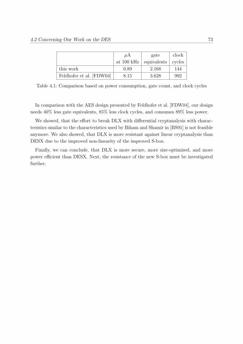
4.2 Concerning Our Work on the DES 73
µA gate clock
at 100 kHz equivalents cycles
this work 0.89 2.168 144
Feldhofer et al. [FDW04] 8.15 3.628 992
Table 4.1: Comparison based on power consumption, gate count, and clock cycles
In comparison with the AES design presented by Feldhofer et al. [FDW04], our design
needs 40% less gate equivalents, 85% less clock cycles, and consumes 89% less power.
We showed, that the effort to break DLX with differential cryptanalysis with charac-
teristics similar to the characteristics used by Biham and Shamir in [BS91] is not feasible
anymore. We also showed, that DLX is more resistant against linear cryptanalysis than
DESX due to the improved non-linearity of the improved S-box.
Finally, we can conclude, that DLX is more secure, more size-optimised, and more
power efficient than DESX. Next, the resistance of the new S-box must be investigated
further.
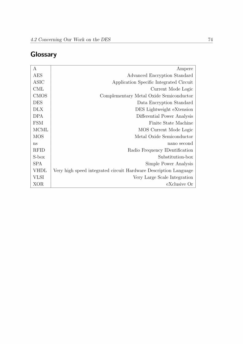
4.2 Concerning Our Work on the DES 74
Glossary
A Ampere
AES Advanced Encryption Standard
ASIC Application Specific Integrated Circuit
CML Current Mode Logic
CMOS Complementary Metal Oxide Semiconductor
DES Data Encryption Standard
DLX DES Lightweight eXtension
DPA Differential Power Analysis
FSM Finite State Machine
MCML MOS Current Mode Logic
MOS Metal Oxide Semiconductor
ns nano second
RFID Radio Frequency IDentification
S-box Substitution-box
SPA Simple Power Analysis
VHDL Very high speed integrated circuit Hardware Description Language
VLSI Very Large Scale Integration
XOR eXclusive Or

Bibliography
[AG00] James R. Armstrong and F. Gail Gray. VHDL Design Representation and
Synthesis. Prentice Hall PTR, second edition, 2000.
[AK96] R. Anderson and M. Kuhn. Tamper Resistance - a Cautionary Note. In Second
Usenix Workshop on Electronic Commerce, pages 1–11, November 1996.
[AO] M. Aigner and E. Oswald. Power Analysis Tutorial.
www.iaik.tugraz.at/aboutus/people/oswald/papers/dpa tutorial.pdf. Sem-
inar paper.
[BB94] Biham and Biryukov. How to Strengthen DES Using Existing Hardware. In
ASIACRYPT: Advances in Cryptology – ASIACRYPT: International Confer-
ence on the Theory and Application of Cryptology. LNCS, Springer-Verlag, 1994.
available for download at citeseer.ist.psu.edu/biham94how.html.
[Bha99] J. Bhasker. A VHDL Primer. Prentice Hall PTR, third edition, 1999.
[BS91] E. Biham and A. Shamir. Differential Cryptanalysis of DES-like Cryptosys-
tems. In A. J. Menezes and S. A. Vanstone, editors, Advances in Cryptology —
CRYPTO ’90, volume LNCS 537, pages 2–21, Berlin, Germany, 1991. Springer-
Verlag.
[BS92] Eli Biham and Adi Shamir. Differential Cryptanalysis of the Full 16-Round
DES. In CRYPTO, pages 487–496, 1992. available for download at citeseer.
ist.psu.edu/biham93differential.html.
[C. 00] C. Clavier, J.-S. Coron and N. Dabbous. Differential Power Analysis in the Pres-
ence of Hardware Countermeasures. In Cryptographic Hardware and Embedded
Systems — CHES 2000, volume 1965 of Lecture Notes in Computer Science,
pages 252–263. Springer Verlag, Berlin, Germany, 2000.

Bibliography 76
[Cop94] D. Coppersmith. The Data Encryption Standard (DES) and its Strength
Against Attacks. Technical report rc 186131994, IBM Thomas J. Watson Re-
search Center, December 1994.
[DR02] Joan Daemen and Vincent Rijmen. The Design of Rijndael: AES - The Advanced
Encryption Standard. Springer Verlag, 2002.
[Eli04] Elisabeth Oswald and Stefan Mangard and Norbert Pramstaller. Secure and
Efficient Masking of AES - A Mission Impossible? Cryptology ePrint Archive,
Report 2004/134, 2004. available for download at http://eprint.iacr.org/.
[FDW04] Martin Feldhofer, Sandra Dominikus, and Johannes Wolkerstorfer. Strong
authentication for RFID systems using the AES algorithm. In Marc Joye and
Jean-Jacques Quisquater, editors, Cryptographic Hardware and Embedded Sys-
tems — CHES 2004, volume 3156 of Lecture Notes in Computer Science, pages
357–370. Springer Verlag, Berlin, Germany, 2004.
[Gla] W. H. Glauert. VHDL tutorial. available for download at http://www.
vhdl-online.de/tutorial.
[How] Howard M. Heys. A Tutorial on Linear and Differential Cryptanalysis. available
for download at www.engr.mun.ca/~howard/PAPERS/ldc_tutorial.pdf.
[I. 05] I. Hatirnaz, S. Badel, Y. Leblebici. Towards a Unified Top-Down Design Flow
For Fully Differential Logic Blocks With Improved Speed and Noise Immunity.
In Proceedings of PRIME05, volume I, pages 63–66, July 2005.
[Ien] Paolo Ienne. Architecture des ordinateurs. available for download at http://
lapwww.epfl.ch/courses/archord1/index.html and http://lapwww.epfl.
ch/courses/archord2/index.html.
[KJJ99] Paul C. Kocher, Joshua Jaffe, and Benjamin Jun. Differential Power Analysis.
In Michael J. Wiener, editor, Advances in Cryptology — CRYPTO ’99, volume
1666 of Lecture Notes in Computer Science, pages 388–397. Springer Verlag,
Berlin, Germany, 1999.
[KLPL94] K. Kim, S. Lee, S. Park, and D. Lee. DES can be immune to linear cryptanaly-
sis, 1994. available for download at citeseer.csail.mit.edu/kim94des.html.
[KLPL95] K. Kim, S. Lee, S. Park, and D. Lee. Securing DES S-boxes Against Three
Robust Cryptanalysis, 1995. available for download at citeseer.ist.psu.edu/
kim95securing.html.
Bibliography 77
[Knu] Lars Ramkilde Knudsen. Iterative Characteristics of DES and s2-DES. available
for download at citeseer.csail.mit.edu/21658.html.
[Koc96] P. Kocher. Timing Attacks on Implementations of Diffie-Hellman, RSA, DSS,
and Other Systems. In Advances in Cryptology — CRYPTO ’96, volume LNCS
1666, pages 104–113. Springer-Verlag, 1996.
[KPL] Kwangjo Kim, Sangjun Park, and Sangjin Lee. Reconstruction of s2-DES S-
Boxes and their Immunity to Differential Cryptanalysis. available for download
at citeseer.csail.mit.edu/kim93reconstruction.html.
[KR01] Joe Kilian and Phillip Rogaway. How to Protect DES Against Exhaustive Key
Search (an Analysis of DESX). Journal of Cryptology: the journal of the Inter-
national Association for Cryptologic Research, 14(1):17–35, 2001. available for
download at citeseer.ist.psu.edu/article/kilian96how.html.
[Mae] Andreas Maeder. VHDL Kompakt. available for download at
http://tams-www.informatik.uni-hamburg.de/vhdl/doc/cookbook/
VHDL-Cookbook.pdf.
[Mat94] M. Matsui. Linear Cryptanalysis of DES Cipher. In T. Hellenseth, editor,
Advances in Cryptology — EUROCRYPT ’93, volume LNCS 0765, pages 286 –
397, Berlin, Germany, 1994. Springer-Verlag.
[MDS99] T. S. Messerges, E. A. Dabbish, and R. H. Sloan. Investigations of Power Anal-
ysis Attacks on Smartcards. In USENIX Workshop on Smartcard Technology,
pages 151–162, 1999.
[Nat99] National Institute of Standards and Technology (NIST). Data Encryption Stan-
dard (DES), October 1999. Federal Information Processing Standards (FIPS)
Publication 46-3.
[Nat01] National Institute of Standards and Technology (NIST). Advanced Encryption
Standard (AES), November 2001. Federal Information Processing Standards
(FIPS) Publication 197.
[Pay03] Payam Heydari. Design and Analysis of Low-Voltage Current-Mode Logic
Buffers. In ISQED, pages 293–298, 2003.
[Pos05] Axel Poschmann. A Semi-Custom, Standard Cell ASIC Implementation of the
Advanced Encryption Standard. available on request. to obtain it send an email
to [email protected], April 2005.

Bibliography 78
[Rij] Vincent Rijmen. Efficient Implementation of the Rijndael SBoxes. available for
download at http://www.iaik.tu-graz.ac.at/research/krypto/AES/old/
~rijmen/rijndael/sbox.pdf.
[S. 05] S. Mangard, N. Pramstaller, and E. Oswald. Successfully Attacking Masked
AES Hardware Implementations. In Josyula R. Rao Berk Sunar, editor, Crypto-
graphic Hardware and Embedded Systems — CHES 2005, volume 3659 of Lecture
Notes in Computer Science, pages 157–171. Springer Verlag, Berlin, Germany,
2005.
[Sch96] B. Schneier. Applied Cryptography. John Wiley & Sons, 2nd edition edition,
1996.
[Sel02] M. Selhorst. Die Geldkarte - Eine sichere elektronische Geldborse?! Seminar
paper, 2002. Universitat Bochum, Germany.
[Smi97] Michael John Sebastian Smith. Application Specific Integrated Circuits.
Addison-Wesley, first edition, 1997.
[Sti02] Douglas R. Stinson. Cryptography: Theory and Practice, Second Edition. Chap-
man & Hall/CRC, February 2002.
[WOL02] Johannes Wolkerstorfer, Elisabeth Oswald, and Mario Lamberger. An ASIC
Implementation of the AES SBoxes. In Bart Preenel, editor, Proceedings of
the Cryptographer’s Track at the RSA Conference 2002, volume 2271 of Lecture
Notes in Computer Science, pages 67–78. Springer Verlag, Berlin, Germany,
2002.