SiC Power Semiconductor Devices for new Applications in ...
8
HAL Id: hal-00373016 https://hal.archives-ouvertes.fr/hal-00373016 Submitted on 13 Oct 2020 HAL is a multi-disciplinary open access archive for the deposit and dissemination of sci- entific research documents, whether they are pub- lished or not. The documents may come from teaching and research institutions in France or abroad, or from public or private research centers. L’archive ouverte pluridisciplinaire HAL, est destinée au dépôt et à la diffusion de documents scientifiques de niveau recherche, publiés ou non, émanant des établissements d’enseignement et de recherche français ou étrangers, des laboratoires publics ou privés. SiC Power Semiconductor Devices for new Applications in Power Electronics Dominique Planson, Dominique Tournier, Pascal Bevilacqua, Nicolas Dheilly, Hervé Morel, Christophe Raynaud, Mihai Lazar, Dominique Bergogne, Bruno Allard, Jean-Pierre Chante To cite this version: Dominique Planson, Dominique Tournier, Pascal Bevilacqua, Nicolas Dheilly, Hervé Morel, et al.. SiC Power Semiconductor Devices for new Applications in Power Electronics. 13th IEEE PEMC, Sep 2008, Poznan, Poland. pp.2457 - 2463, 10.1109/EPEPEMC.2008.4635632. hal-00373016
Transcript of SiC Power Semiconductor Devices for new Applications in ...

HAL Id: hal-00373016https://hal.archives-ouvertes.fr/hal-00373016
Submitted on 13 Oct 2020
HAL is a multi-disciplinary open accessarchive for the deposit and dissemination of sci-entific research documents, whether they are pub-lished or not. The documents may come fromteaching and research institutions in France orabroad, or from public or private research centers.
L’archive ouverte pluridisciplinaire HAL, estdestinée au dépôt et à la diffusion de documentsscientifiques de niveau recherche, publiés ou non,émanant des établissements d’enseignement et derecherche français ou étrangers, des laboratoirespublics ou privés.
SiC Power Semiconductor Devices for new Applicationsin Power Electronics
Dominique Planson, Dominique Tournier, Pascal Bevilacqua, Nicolas Dheilly,Hervé Morel, Christophe Raynaud, Mihai Lazar, Dominique Bergogne, Bruno
Allard, Jean-Pierre Chante
To cite this version:Dominique Planson, Dominique Tournier, Pascal Bevilacqua, Nicolas Dheilly, Hervé Morel, et al.. SiCPower Semiconductor Devices for new Applications in Power Electronics. 13th IEEE PEMC, Sep2008, Poznan, Poland. pp.2457 - 2463, �10.1109/EPEPEMC.2008.4635632�. �hal-00373016�
SiC Power Semiconductor Devices for new
Applications in Power Electronics
Dominique Planson∗, Dominique Tournier, Pascal Bevilacqua, Nicolas Dheilly, Herve Morel,
Christophe Raynaud, Mihai Lazar, Dominique Bergogne, Bruno Allard, Jean-Pierre Chante∗Ampere Lab INSA Lyon, F-69621 Villeurbanne Cedex, France, e-mail: [email protected]
Abstract— This paper addresses the benefits of SiC semi-conductor, owning excellent physical properties able to fulfillnew scope of applications in terms of high temperature,high voltage and for more specific applications. Devices andapplications developed at Ampere laboratory are detailed.
Keywords— SiC-device, High temperature electronics,Power semiconductor device, High voltage Device, Powerintegrated circuit.
I. INTRODUCTION
The first unipolar power silicon carbide devices (Schot-
tky diodes) were commercialized in 2001 [1], [2]. Nowa-
days power JFETs are available as engineering samples
[3], [4] . These two devices enable to build a large
number of power switching converters. It is worth listing
the scope of applications for which silicon carbide de-
vices can advantageously replace classical silicon power
semiconductor devices. The first kind of applications for
SiC power devices are applications for which the use
of silicon is impossible or restricted. The second kind
of applications for SiC devices correspond to systems in
which mass reduction is a key issue, e.g. for embedded
systems like in transport.
Fig. 1. On state resistance for unipolar devices for various semiconduc-tor materials.
Figure 1 illustrates the on-state resistance for differ-
ent semiconductor materials. It yields the optimal on-
resistance limit versus breakdown voltage of an infi-
nite plane junction for different semiconductor materials.
These are theoretical limits. Stars correspond to power
device demonstrators. It is clear that there are over the
theoretical limit of Si and also from the SiC limits. From
this figure, it is clear that there is still a great margin to get
the optimal performances of SiC devices.So, clearly, SiC
power device applications are high temperature and/or
high voltage applications. However, most of recent studies
have shown that the use of SiC devices does not consist in
a simple replacement of silicon devices by silicon carbide
devices. Indeed a new design of power electronic systems
must take advantage of the properties of the new SiC
power devices.
II. HIGH VOLTAGE APPLICATIONS
Such applications are medium term applications be-
cause high voltage devices are not ready for industrial
applications. However 10 kV demonstrators have been
developed, 15kV demonstrators are under development
even 30kV and further may soon be obtained. The interest
in such devices is huge since they enable to :
• replace heavy 50Hz high voltage electrical trans-
formers by high voltage static power electronics.
• replace AC-current distribution networks by DC-
current distribution networks and eliminating numer-
ous associated problems like instability (wind-power
farm ...) even blackout. This enables an easier inte-
gration of renewable energy sources (Photovoltaic,
Wing power...) and removes the need of 50Hzelectric transformers.
• improve the high voltage system protection with very
fast active protection systems.
The main issues of these new applications are :
• availability of high bipolar diodes and switches (BJT,
Thyristors, ...),
• electrical insulation of the high voltage converters
(packaging, passivation, ...),
• thermal cooling of the high voltage converters,
highly insulated driver for high voltage converters
even multi-level converters.
Ampere lab works are divided in several tasks:
A. Design of high voltage periphery protection
Design of efficient peripheral protection is fundamental
for high voltage devices. This protection should have an
optimum geometry in order to avoid local critical electric
field areas. There are various possible protections such as
JTE (Junction Termination Extension), Mesa, field plates
2488
978-1-4244-1742-1/08/$25.00 c© 2008 IEEE

or guard rings [5]. Design of classical JTE needs an
accurate control of the doping dose to reach the complete
depletion of the termination well for a given reverse
voltage (VBR). The peripheral protection efficiency is the
ratio between breakdown voltage of the protected diode
and of the ideal diode (plane parallel junction), this last
being named theoretical breakdown voltage afterwards.
JTE process for SiC device is most often an ionic implan-
tation followed by a thermal annealing. Figure 2 shows
the breakdown voltage of a bipolar diode against the
termination doping dose for several JTE lengths.
Fig. 2. Breakdown voltage against implanted dose for a constant lateraldoping profile and for several JTE lengths.
With an epitaxial layer thickness of 50μm and a doping
level of 1015cm−3, the diode is able to sustain 7.5kV .
The JTE depth is 0.8μm. As can be observed from Figure
1, breakdown voltage is very sensitive to the implanted
dose. Besides this voltage is almost independent from the
well length if the JTE is longer than 100μm. The break-
down voltage is calculated by numerical bi-dimensional
simulation using MEDICITM software [6] and impact
ionization coefficients published by Konstantinov [7].
VBR is defined as the voltage involving a leakage current
of 1μA.μm−1. JTE with variable lateral doping is a
good way to get an efficient protection valid for a wide
range of doping concentration. Thanks to the diffusion
process, it is possible to realise this kind of JTE in silicon.
However, due to the lack of dopant diffusion in SiC,
variable doping JTE is very difficult to obtain. A good
alternative is a JTE with multiple constant doping zones to
approximate the optimum lateral profile. Figure 3 presents
a SiC bipolar diode protected by a three-zone JTE that has
been optimized to achieve a breakdown voltage that is as
close as possible to the theoretical breakdown voltage.
Each zone is defined by its doping dose Di and its
length Xi. Figure 4 shows 5 possible configurations of
doping variation of the three zones enabling a VBR of
7500 V i.e. 99% of the theoretical breakdown voltage.
The highest doped zone is the first one and its variation
range is the widest. For the two other zones, dose choices
are more critical, because of the wider D2 variation range,
and of the narrower D3 one.
A 7500 V breakdown voltage can be obtained using
Fig. 3. Vertical cross-section of the triple JTE (D1, D2 and D3)protected diode.
Fig. 4. Five possible dose configurations and their variation ranges toobtain a 99% protection efficiency.
simple or triple JTE. Nevertheless the latter option (which
is a discretization of the ideal variable lateral doping
profile) enables a larger flexibility on doping concentra-
tions. The only drawback of this technique is a little more
complicated technological process.
B. Fabrication of high voltage bipolar devices
The aim of this study is to show potentialities of silicon
carbide for high voltage power systems. Test structures
are SiC bipolar diodes able to sustain 1.3kV and 5kV .
Emitter and periphery protection (JTE) are obtained by
ion implantation of Aluminium in epitaxial n-type layer
grown on commercial substrate. The number of devices
which exhibit efficiency > 84% has been improved during
the last four years. Indeed 70% of the 1.3kV diodes with
an emitter implanted at 300˚C and a long JTE (120 m)
exhibit a breakdown voltage higher than 1100V (up to
1300V ) without any impact of the ambient conditions (air
or SF6 gas or dielectric liquid). The ambient conditions
impact breakdown voltage only for diodes with short JTE
length (50m) [8]. These results show in the same time that
post-implantation annealing realized in the lab furnace [8]
allows a full activation of dopants in JTE. In forward
state, current densities and efficiency have been improved
2008 13th International Power Electronics and Motion Control Conference (EPE-PEMC 2008) 2489

(200 A/cm2 @ 5 V at room temperature) also due to
the improvement of metallization step and subsequent
annealing at IMM Bologne [9]. Results of acceptable
ohmic contacts on highly doped P+ zones are comparable
with other results already published in literature [10]. As
it can be observed in Figure 5, Ampere-lab is now able
to present results of breakdown voltage in the range of 4
kV, with a maximum of 4.8 kV with low reverse current
density in fluoride ambient (Galden and SF6) [11].
Fig. 5. Reverse I-V characteristics of 5kV bipolar diodes measuredin three different ambient conditions: air, galden and SF6. Active areaA = 0.05mm2.
Without passivation, breakdown voltage is only 1.3kVfor these devices with a JTE length of 250m (optimized
with respect to the semiconductor properties). This clearly
proves the need for passivation in order to fully take
benefit of SiC properties for high voltage applications.
Theoretical interest to use passivation materials with high
dielectric permittivity (ε) in order to reduce electric field
outside SiC have been shown using simulation software
MEDICI on a 5 kV bipolar diode protected by JTE. For
a given structure, only a sufficiently high ε value allows
to reduce electric field peaks both at emitter and JTE
extremities, by stretching space charge region outside the
JTE [12]. Another advantage to use a high ε material
is to significantly reduce the sensitivity on breakdown
voltage with respect to the optimal dose of JTE. From the
technological point of view, choice of such material (with
high ε) and a compatible deposition method remains to
be solved before obtaining experimental results. Among
available and practical insulating materials, polyimide
materials specifications exhibit good dielectric together
with good thermal properties under usual conditions. Thus
an experimental characterization using MIM and MIS
structures has been launched in order to quantify their
effective characteristics within an extended temperature
range. For high voltage (up to 50kV ) and high tempera-
ture (up to 500˚C) measurements, a specific set-up has
to be developed.
1) Fabrication of high voltage thyristor: Since silicon
based technology is reaching its physical limits concern-
ing blocking and power handling capability, GTO thyris-
tors based on SiC are under investigation for compact
future pulsed power systems [13]. Reaching breakdown
voltages of 19kV [14], the potential of SiC based devices
appears very interesting. According to primary device
simulations using the finite element code MEDICITM,
the developed GTO-thyristors should be able to block
voltages up to 6kV . For the device realization, a n-
type 4H-SiC wafer material is obtained from Cree Re-
searchTM, including a PP − NP+ (from the wafer up
to the top) epitaxial layer structure (6). Anode P+ type
Fig. 6. Thyristor structure with planar electrodes for anode and gateand combined periphery protection: MESA and JTE
and gate N+ type layers were obtained by Aluminium
(Al) and Nitrogen (N ) ion implantation doping followed
by a high temperature annealing in the 1700˚C/30minrange in order to activate the dopants. Mesa structures
were fabricated by Reactive Ion Etching with Ni masks
with a particular attention to avoid micromasking forma-
tion and preserving the initial roughness of the surface.
Ohmic contacts are formed by deposing layers composed
on Al/Ni/T i alloys followed by a RTA annealing at
1000˚C during 1 to 2 min. Measurements have been
performed on chip, in oil and as shown in Figure 7 a
breakdown voltage of nearly 5kV has been reached.
Fig. 7. Forward blocking characteristics of the device.
2490 2008 13th International Power Electronics and Motion Control Conference (EPE-PEMC 2008)
III. SPECIFIC APPLICATIONS USING SIC DEVICES
The ability for SiC devices to operate in the high tem-
perature range, 250˚C up to 600˚C allows applications
not possible with conventional silicon devices, especially
for mains-operated systems.
A. Current limiting devices
To protect power electronic circuits against over-current
or over-voltage either serial protection (SP) or a parallel
protection (PP) can be used. For the serial protection
(8, usually used components are Serial Protection Device
(SPD) or Current Limiting Device (CLD), being either
fuses, mechanical contactors, superconductors or poly-
mers.
Fig. 8. Circuit using the protecting device
In all cases it is necessary to dissipate the overload
energy through the protection device which has to sus-
tain high voltage and high current simultaneously. These
constraints imply a very fast temperature increase. So,
when the protection device is active it has to sustain high
junction temperature. All these constraints will globally
define the electrical specifications of this kind of device.
Up to now, only few semiconductor current limiter struc-
tures have been described in the literature [17], [16].
Although Current Regulative Diode components already
exist, their voltage and current capabilities (VBR = 100V ,
IMAX = 10mA), do not allow to use them in power
systems. A promising application of SiC-based devices
is current limitation for power system protection, which
benefits from its high thermal conductivity and wide band
gap. In the steady state operating mode (or passive state),
the voltage drop across the component must be as low as
possible. In the active state, (limiting phase), the current
limiter must sustain a high current, under high voltage
bias. The resulting high power density must not cause the
component failure. Two specific current limiting devices
(CLD) have been studied [18], [20], [19] taking into
account previous considerations.
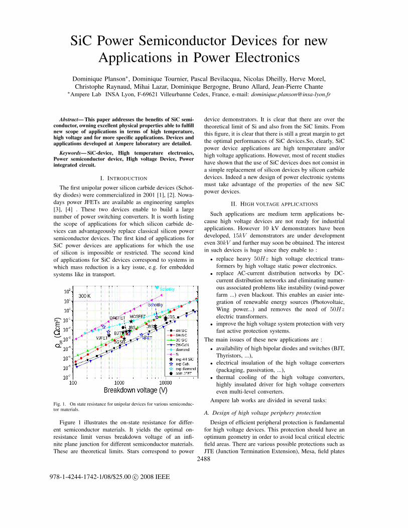
Figure 9 shows a cross section schema of the VJFET
and the main parameters to adjust. This device has a
channel divided in two parts: a vertical one and a lateral
one. The source is grounded and current flows from drain
to source. P-buried layers are designed so that the VJFET
is normally-on and presents a low specific resistance.
When the drain voltage rises, the current saturates at a
voltage corresponding to the pinch-off of both vertical and
horizontal channels. In the saturation mode, the device
Fig. 9. VJFET parameters to be optimized.
presents an important on resistance (RON ), resulting from
the serial resistance of both parts of the channel and the
drift resistance of the epitaxial layer. Due to self heating,
current decreases as the voltage increases (since electron
mobility decreases and induces a current reduction). This
effect is amplified while increasing the limiting current
density. When a negative bias is applied between gate
and source, the PN junction formed by the Pwell and
the epitaxial layer is reverse biased leading to current
modulation. The device optimization job consists in the
design of buried layer (the gate electrode of the devices,
which is formed by either high energy implantation or
epitaxial process), and the tuning of horizontal channel
parameters. A trade off between specific resistance and
blocking capabilities was investigated by means of ana-
lytical model and finite element simulations.
Fig. 10. JFET structure with its parameters.
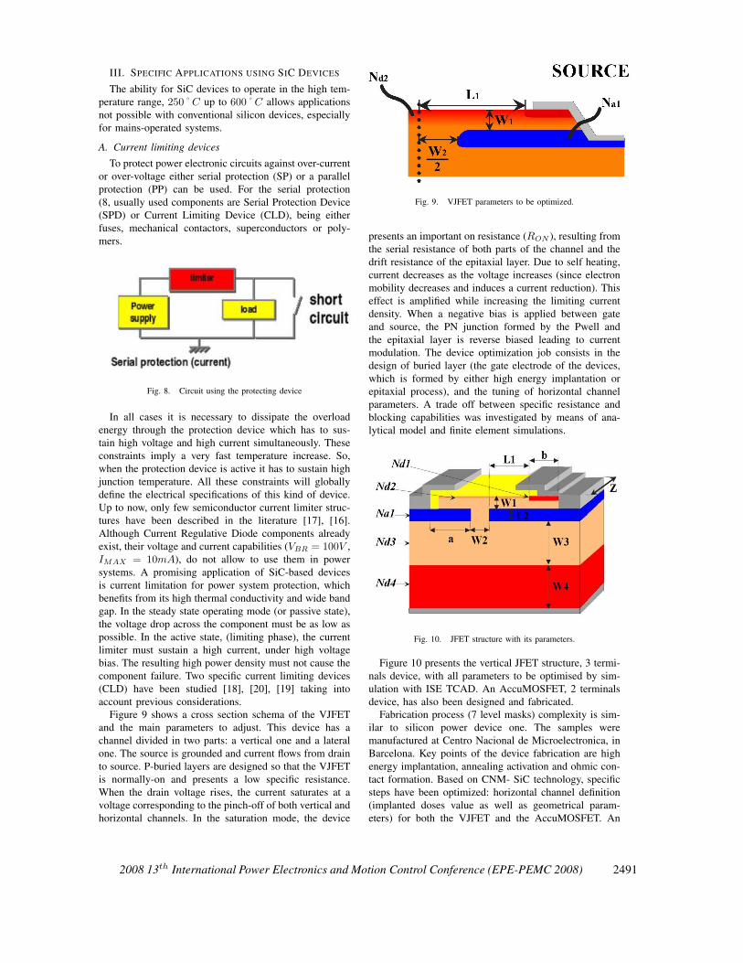
Figure 10 presents the vertical JFET structure, 3 termi-
nals device, with all parameters to be optimised by sim-
ulation with ISE TCAD. An AccuMOSFET, 2 terminals
device, has also been designed and fabricated.
Fabrication process (7 level masks) complexity is sim-
ilar to silicon power device one. The samples were
manufactured at Centro Nacional de Microelectronica, in
Barcelona. Key points of the device fabrication are high
energy implantation, annealing activation and ohmic con-
tact formation. Based on CNM- SiC technology, specific
steps have been optimized: horizontal channel definition
(implanted doses value as well as geometrical param-
eters) for both the VJFET and the AccuMOSFET. An
2008 13th International Power Electronics and Motion Control Conference (EPE-PEMC 2008) 2491
additional step has been tuned for the AccuMOSFET:
the MOSFET channel oxide layer. First batch of small
area devices has been fabricated. Figure 11 presents the
Fig. 11. Electrical measured characteristics for unidirectional and bi-directional limiter.
measured electrical characteristics for an unidirectional
VJFET. Measurements were done by applying 0.5s pulse
(f = 2Hz), with drain biased up to 400 V. The specific
on-resistance varies from 176mΩ.cm2 up to 237mΩ.cm2.
The maximum pulsed power density dissipated by the
CLD in the limiting mode is 160kW/cm2. Limiting capa-
bilities have also been measured for a bi-directional device
made of two unidirectional devices connected head to tail
(i.e. drain connected). This one exhibits a specific on-
resistance of 700mΩ.cm2. Highest breakdown in current
limiting state were measured to be 810V , corresponding
to a high pulsed power density of 140kW/cm2. As it can
be observed from Figure 12, the current limiting device
is able to react in a very short time (less than 1μs).
Fig. 12. Switching waveforms of the current limiter with gate control.
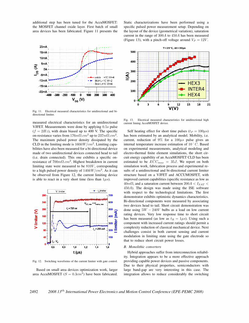
Based on small area devices optimization work, larger
area AccuMOSFET (S = 0.3cm2) have been fabricated.
Static characterizations have been performed using a
specific pulsed power measurement setup. Depending on
the layout of the device (geometrical variation), saturation
current in the range of 300A to 450A has been measured
(Figure 13), with a pinch-off voltage around VP = 12V .
Fig. 13. Electrical measured characteristics for unidirectional highcurrent liming AccuMOSFET device.
Self heating effect for short time pulses (tP = 100μs)
has been estimated by an analytical model. Mobility, i.e.
current, reduction of 9% for a 100μs pulse gives an
internal temperature increase estimation of 10˚C. Based
on experimental measurements, analytical modeling and
electro-thermal finite element simulations, the short cir-
cuit energy capability of an AccuMOSFET CLD has been
estimated to be ECCmax = 35J . We report on both
simulation work, fabrication process and experimental re-
sults of a unidirectional and bi-directional current limiter
structure based on a VJFET and ACCUMOSFET, with
improved current capabilities (specific resistance as low as
40mΩ, and a saturation current between 200A < ISAT <450A). The design was made using the ISE software
with respect to the technological limitations. The first
demonstrator exhibits optimistic dynamics characteristics.
Bi-directional components were measured by associating
two devices head to tail. Short circuit demonstration was
done using 5W − 240V bulbs as a load on low current
rating devices. Very low response time to short circuit
has been measured (as low as tR = 1μs). Using such a
component with increased current ratings should permit a
complexity reduction of classical mechanical device. Next
challenges consist in both current sensing and current
modulation in limiting state using the gate electrode so
that to reduce short circuit power losses.
B. Monolithic converters
Hybrid approaches suffer from interconnection reliabil-
ity. Integration appears to be a more effective approach
providing capable power devices and passive components.
Due to their physical properties, semiconductors with
large band-gap are very interesting in this case. The
integration allows to reduce considerably the switching
2492 2008 13th International Power Electronics and Motion Control Conference (EPE-PEMC 2008)

time and to reduce losses and parasitics related to the
device interconnections. This integrated system based on
the design of SiC lateral JFET with a breakdown voltage
of 900V is presented in Figure 14.
Fig. 14. Schematic presentation of the SiC lateral JFET with a doubleRESURF structure.
In order to improve the blocking voltage and to reduce
the Ron-resistance, the RESURF technique [15] is applied
in this work to design SiC lateral JFETs. The P+typeregion (gate), N+type region (source and drain), N type
active layer and P − type top layer are realized by
ion implantation. The epitaxial layer at the top of the
substrate is defined by a P − type region with a uniform
doping concentration. A double-junction is created in
the top and the bottom of the active n − type layer,
improving its lateral depletion and allowing increasing
of its doping. The n − type active layer constituting the
JFET channel, this technique allows to obtain a JFET
with higher channel doping and so a lower on-resistance
by keeping a high VBR. A relationship between the
doping concentration and the thickness of layers must be
respected to vertically deplete both the p− type top layer
and n − type channel layer before the lateral junction
breakdown. The structure of these devices was studied
with MEDICITM . In each area of the device structure,
different parameters are defined such as profile and con-
centration of doping impurities which were estimated by
Monte-Carlo simulations taking into account the 4H-SiC
crystalline structure. The lateral JFET is a normally-on
device. A negative gate voltage is required to turn the
device off. The channel doping is 2.1017cm−3 and its
thickness is 0.40μm which is smaller than the thickness
of the depleted region produced by the applied drain-to-
source voltage. The thickness of the p − type top layer
is 0.12μm The potential line distributions in the double
RESURF SiC JFET in forward blocking mode are shown
in Figure 15 for different doping concentrations of the top
layer varying from 5.1016cm−3 to 5.1017cm−3.
The VBR variation is also presented in Figure 16. The
potential lines are distributed mainly in the p-type epi-
layer due to the low doping concentration of this layer.
The presence of the top layer with a low doping concen-
tration (5.1016cm−3 -Figure 15-a) generates a potential
line distribution transversally at the device surface. In this
Fig. 15. Potential distribution for the lateral JFETwith a doping concentration of the Ptop layer :5.1016cm3(a), 1.1017cm3(b), 2.1017cm3(c)and5.1017cm3(d)
case, the value of blocking voltage is equal to 385V . In
the same way, a high doping concentration of the top layer
with a high doping concentration (5.1017cm3 - Figure
15-d) makes difficult to deplete this layer. The maximum
value of electric field is obtained at the drain side. In this
case, the potential lines are concentrated that involves the
device to reach prematurely the blocking voltage.
The potential distribution is optimum, when the doping
concentration of the top layer ranges between 1017cm−3
and 2.1017cm−3, thus obtaining a trapezoidal electric
field profile between the drain and the gate. In this case,
the Space Charge Region (SCR) surface is wider when he
VBR of the JFET is increased up to 1kV , as presented
in Figure 16.
Fig. 16. VBR versus top layer doping for the JFET structure.
The lateral JFETs run is performed (Figure 17). The
first results show that in blocking state, the RESURF
structures are validated in terms of voltage rating. Break-
down voltage values as high as 600V were obtained which
is conform to the specific requirements for which these
2008 13th International Power Electronics and Motion Control Conference (EPE-PEMC 2008) 2493

Fig. 17. Top view of the SiC lateral JFETs with different inter-digitatedstructures and different sizes.
devices have been designed.
IV. CONCLUSION
This paper shows the already existing devices and
applications using SiC devices. Higher theoretical values
could be reached but the environment of the devices
remains a critical issue. Dealing with Current Limiting
Devices, although we demonstrate they are able to sustain
high current densities, the packaging and interconnections
are limiting their performances. It seems to be clear that
for high voltage devices, the periphery protection must
now combine several classical techniques, and must take
into account the passivation features (dielectric permit-
tivity, thicknesses and interface states density). There is
still works to be done to reach the real performances of
SiC semiconductor material, for the fabrication of high
voltage, high temperature and integrated power systems.
ACKNOWLEDGMENT
The authors would like to thank all the financial support
from different institutions and companies, namely DGA,
CNRS, ISL, Schneider-Electric, ST micro-electronics,
Alstom and Hispano-Suiza. Authors also gives special
thanks to Philippe Godigon of the “Centro Nacional
de Microelectronica” of Barcelona for clean-room SiC-
process support.
REFERENCES
[1] D. Stephani, Status, prospects and commercialization of SiC powerdevices. Device Research Conference, in proceedings, p14, 2001.
[2] http://www.cree.com[3] S. Round, M. Heldwein, J. Kolar I. Hofsajer P. Friedrichs, A SiC
JFET Driver for a 5 kW, 150 kHz Three-Phase PWM Converter,IAS Conference, p 410-416, 2005.
[4] http://www.siced.de[5] B.J. Baliga, “Modern Power Devices”, New York : Wiley, 1987[6] Technology Modeling Associates, Inc. MEDICI: Two dimension-
nal semiconductor device simulation, Version 2005.2.0, Vol. 1 etVol. 2, 2005
[7] ]A. O. Konstantinov, Q. Wahab, N. Nordell, U. Lindefelt. Ioniza-tion Rates and Critical Fields in 4H-SiC Junction devices, Appl.
Phys. Lett. 71, 1, 1997, p. 90-92
[8] M. Lazar, G. Cardinali, C. Raynaud, A. Poggi, D. Planson, R.Nipoti, J.P. Chante, The role of the ion implanted emitter stateon 6H-SiC power diodes behavior. A statistical study, 2004 -Materials Science Forum, vol. 457-460, p. 1025-1028
[9] R. Nipoti, F. Moscatelli, A. Scorzoni, A. Poggi, G. C. Cardinali,M. Lazar, C. Raynaud, D. Planson, M-L. Locatelli, J-P. Chante,Contact Resistivity of Al/Ti Ohmic Contacts on p-Type Ion Im-planted 4H- and 6H-SiC, MRS Proceedings vol. 742, 2002 Fall,
p. K6.2
[10] J. Crofton, S. E. Mohney, J.R. Williams, T. Isaacs-Smith, Findingthe Optimum Al-Ti Alloy Composition for Use as an OhmicContact to P-Type SiC, 2002, Solid State Electronics, vol. 46, No.
1, pp 109-113,[11] C. Raynaud, M. Lazar, D. Planson, J.P. Chante, Z. Sassi Design,
fabrication and characterization of 5 kV 4H-SiC p+n planar bipolardiodes protected by junction termination extension 2004 Materials
Science Forum, vol. 457-460, p. 1033-1036.
[12] M.L. Locatelli, K. Isoird, S. Dinculescu, V. Bley, T. Lebey, D.Planson, E. Dutarde, M. Mermet-Guyennet, ”Study of suitabledielectric material properties for high electric field and high tem-perature power semiconductor environment”, EPE’03 conference,
2-4 Sept 2003, Toulouse, France.[13] S. Scharnholz, V. Zorngiebel, P. Brosselard, and E. Spahn; in IEE
Proc. of the 1st European Pulsed Power Symposium (EPPS), 22-24October 2002, Saint Louis, France; 2002; p. 14/1-14/6.
[14] Y. Sugawara, D. Takayama, K. Asano, R. Singh, J. Palmour,T. Hayashi 1219 kV 4H-SiC pin diodes with low power loss,Proceedings of 2001 International Symposium on Power Semi-
conductor Devices & Ics, Osaka, p. 27-30[15] Adriaan W. Ludikhuize ”A Review of RESURF Technology”
ISPSD’2000 Toulouse. France, p. 11-18[16] Siemens Corp. Current limiter circuit, Patent n W09727657,
30/07/97,[17] J.L. Sanchez et al., Design and fabrication of a new high voltage
current limiting device for serial protection applications, Proc. 8th
International Symposium on Power Semiconductor Devices and
ICs, ISPSD96, Hawai, USA, 1996, pp. 201-205.[18] D. Tournier et. al. Current limitation with SiC devices, in proceed-
ings of 2002 EPE conference, Toulouse 2002.[19] Nallet, F. et. al. ,Very low R/sub ON/ measured on 4H-SiC accu-
MOSFET high power device, Power Semiconductor Devices and
ICs, 2002. Proceedings of the 14th International Symposium on,
2002, pp. 209- 212[20] D. Tournier et. al., Optimal layout for 6HSiC VJFET controlled
current limiting device, Diamond and Related Materials Volume
12, Issues 3-7, March-July 2003, Pages 1220-1223
2494 2008 13th International Power Electronics and Motion Control Conference (EPE-PEMC 2008)