Si5351A/B/C Data Sheet
72
Preliminary Rev. 0.95 8/11 Copyright © 2011 by Silicon Laboratories Si5351A/B/C This information applies to a product under development. Its characteristics and specifications are subject to change without notice. Si5351A/B/C I 2 C-P ROGRAMMABLE A NY -F REQUENCY CMOS C LOCK G ENERATOR + VCXO Features Applications Description The Si5351 is an I 2 C configurable clock generator that is ideally suited for replacing crystals, crystal oscillators, VCXOs, phase-locked loops (PLLs), and fanout buffers in cost-sensitive applications. Based on a PLL/VCXO + high resolution MultiSynth fractional divider architecture, the Si5351 can generate any frequency up to 160 MHz on each of its outputs with 0 ppm error. Three versions of the Si5351 are available to meet a wide variety of applications. The Si5351A generates up to 8 free-running clocks using an internal oscillator for replacing crystals and crystal oscillators. The Si5351B adds an internal VCXO and provides the flexibility to replace both free-running clocks and synchronous clocks. The Si5351B eliminates the need for higher cost, custom pullable crystals while providing reliable operation over a wide tuning range. The Si5351C offers the same flexibility but synchronizes to an external reference clock (CLKIN). Functional Block Diagram Generates up to 8 non-integer-related frequencies from 8 kHz to 160 MHz I 2 C user definable configuration Exact frequency synthesis at each output (0 ppm error) Highly linear VCXO Optional clock input (CLKIN) Low output period jitter: 100 ps pp Configurable spread spectrum selectable at each output Operates from a low-cost, fixed frequency crystal: 25 or 27 MHz Supports static phase offset Programmable rise/fall time control Glitchless frequency changes Separate voltage supply pins: Core VDD: 2.5 or 3.3 V Output VDDO: 1.8, 2.5, or 3.3 V Excellent PSRR eliminates external power supply filtering Very low power consumption Adjustable output-output delay Available in 3 packages types: 10-MSOP: 3 outputs 24-QSOP: 8 outputs 20-QFN (4x4 mm): 8 outputs PCIE Gen 1 compliant Supports HCSL compatible swing HDTV, DVD/Blu-ray, set-top box Audio/video equipment, gaming Printers, scanners, projectors Residential gateways Networking/communication Servers, storage XO replacement Si5351A Multi Synth N N = 2 or 7 I 2 C SSEN OEB Multi Synth 0 Multi Synth 1 Si5351B PLL VC VCXO I 2 C SSEN OEB Multi Synth 0 Multi Synth 1 Multi Synth 2 Multi Synth 3 Multi Synth 4 Multi Synth 5 Multi Synth 6 Multi Synth 7 Si5351C PLLA CLKIN PLLB I 2 C INTR OEB Multi Synth 0 Multi Synth 1 Multi Synth 2 Multi Synth 3 Multi Synth 4 Multi Synth 5 Multi Synth 6 Multi Synth 7 XA XB OSC XA XB OSC PLLB PLLA XA XB OSC Ordering Information: See page 66 10-MSOP 24-QSOP 20-QFN
Transcript of Si5351A/B/C Data Sheet

Preliminary Rev. 0.95 8/11 Copyright © 2011 by Silicon Laboratories Si5351A/B/CThis information applies to a product under development. Its characteristics and specifications are subject to change without notice.
Si5351A/B/C
I2C-PROGRAMMABLE ANY-FREQUENCY CMOS CLOCK GENERATOR + VCXOFeatures
Applications
Description
The Si5351 is an I2C configurable clock generator that is ideally suited for replacingcrystals, crystal oscillators, VCXOs, phase-locked loops (PLLs), and fanout buffers incost-sensitive applications. Based on a PLL/VCXO + high resolution MultiSynth fractionaldivider architecture, the Si5351 can generate any frequency up to 160 MHz on each of itsoutputs with 0 ppm error. Three versions of the Si5351 are available to meet a widevariety of applications. The Si5351A generates up to 8 free-running clocks using aninternal oscillator for replacing crystals and crystal oscillators. The Si5351B adds aninternal VCXO and provides the flexibility to replace both free-running clocks andsynchronous clocks. The Si5351B eliminates the need for higher cost, custom pullablecrystals while providing reliable operation over a wide tuning range. The Si5351C offersthe same flexibility but synchronizes to an external reference clock (CLKIN).
Functional Block Diagram
Generates up to 8 non-integer-related frequencies from 8 kHz to 160 MHz
I2C user definable configuration Exact frequency synthesis at each output
(0 ppm error) Highly linear VCXO Optional clock input (CLKIN) Low output period jitter: 100 ps pp Configurable spread spectrum selectable
at each output Operates from a low-cost, fixed frequency
crystal: 25 or 27 MHz Supports static phase offset Programmable rise/fall time control
Glitchless frequency changes Separate voltage supply pins:
Core VDD: 2.5 or 3.3 VOutput VDDO: 1.8, 2.5, or 3.3 V
Excellent PSRR eliminates external power supply filtering
Very low power consumption Adjustable output-output delay Available in 3 packages types:
10-MSOP: 3 outputs24-QSOP: 8 outputs20-QFN (4x4 mm): 8 outputs
PCIE Gen 1 compliant Supports HCSL compatible swing
HDTV, DVD/Blu-ray, set-top box Audio/video equipment, gaming Printers, scanners, projectors
Residential gateways Networking/communication Servers, storage XO replacement
Si5351A
Multi Synth
N
N = 2 or 7
I2C
SSENOEB
Multi Synth
0
Multi Synth
1
Si5351B
PLL
VC VCXO
I2C
SSENOEB
Multi Synth
0
Multi Synth
1
Multi Synth
2
Multi Synth
3
Multi Synth
4
Multi Synth
5
Multi Synth
6
Multi Synth
7
Si5351C
PLLA
CLKINPLLB
I2C
INTROEB
Multi Synth
0
Multi Synth
1
Multi Synth
2
Multi Synth
3
Multi Synth
4
Multi Synth
5
Multi Synth
6
Multi Synth
7
XA
XB
OSC
XA
XB
OSC
PLLB
PLLAXA
XB
OSC
Ordering Information:
See page 66
10-MSOP
24-QSOP
20-QFN

Si5351A/B/C
2 Preliminary Rev. 0.95
Si5351A/B/C
Preliminary Rev. 0.95 3
TABLE OF CONTENTS
Section Page
1. Electrical Specifications . . . . . . . . . . . . . . . . . . . . . . . . . . . . . . . . . . . . . . . . . . . . . . . . . . .42. Detailed Block Diagrams . . . . . . . . . . . . . . . . . . . . . . . . . . . . . . . . . . . . . . . . . . . . . . . . . . .93. Functional Description . . . . . . . . . . . . . . . . . . . . . . . . . . . . . . . . . . . . . . . . . . . . . . . . . . .11
3.1. Input Stage . . . . . . . . . . . . . . . . . . . . . . . . . . . . . . . . . . . . . . . . . . . . . . . . . . . . . . . .113.2. Synthesis Stages . . . . . . . . . . . . . . . . . . . . . . . . . . . . . . . . . . . . . . . . . . . . . . . . . . .123.3. Output Stage . . . . . . . . . . . . . . . . . . . . . . . . . . . . . . . . . . . . . . . . . . . . . . . . . . . . . . .123.4. Spread Spectrum . . . . . . . . . . . . . . . . . . . . . . . . . . . . . . . . . . . . . . . . . . . . . . . . . . .133.5. Control Pins (OEB, SSEN) . . . . . . . . . . . . . . . . . . . . . . . . . . . . . . . . . . . . . . . . . . . .13
4. I2C Interface . . . . . . . . . . . . . . . . . . . . . . . . . . . . . . . . . . . . . . . . . . . . . . . . . . . . . . . . . . . .145. Configuring the Si5351 . . . . . . . . . . . . . . . . . . . . . . . . . . . . . . . . . . . . . . . . . . . . . . . . . . .16
5.1. Writing a Custom Configuration to RAM . . . . . . . . . . . . . . . . . . . . . . . . . . . . . . . . . .165.2. Si5351 Application Examples . . . . . . . . . . . . . . . . . . . . . . . . . . . . . . . . . . . . . . . . . .185.3. Replacing Crystals and Crystal Oscillators . . . . . . . . . . . . . . . . . . . . . . . . . . . . . . . .185.4. Replacing Crystals, Crystal Oscillators, and VCXOs . . . . . . . . . . . . . . . . . . . . . . . .195.5. Replacing Crystals, Crystal Oscillators, and PLLs . . . . . . . . . . . . . . . . . . . . . . . . . .195.6. Replacing a Crystal with a Clock . . . . . . . . . . . . . . . . . . . . . . . . . . . . . . . . . . . . . . . .205.7. HCSL Compatible Outputs . . . . . . . . . . . . . . . . . . . . . . . . . . . . . . . . . . . . . . . . . . . .20
6. Design Considerations . . . . . . . . . . . . . . . . . . . . . . . . . . . . . . . . . . . . . . . . . . . . . . . . . . .216.1. Power Supply Decoupling/Filtering . . . . . . . . . . . . . . . . . . . . . . . . . . . . . . . . . . . . . .216.2. Power Supply Sequencing . . . . . . . . . . . . . . . . . . . . . . . . . . . . . . . . . . . . . . . . . . . .216.3. External Crystal . . . . . . . . . . . . . . . . . . . . . . . . . . . . . . . . . . . . . . . . . . . . . . . . . . . . .216.4. External Crystal Load Capacitors . . . . . . . . . . . . . . . . . . . . . . . . . . . . . . . . . . . . . . .216.5. Unused Pins . . . . . . . . . . . . . . . . . . . . . . . . . . . . . . . . . . . . . . . . . . . . . . . . . . . . . . .216.6. Trace Characteristics . . . . . . . . . . . . . . . . . . . . . . . . . . . . . . . . . . . . . . . . . . . . . . . .22
7. Register Map Summary . . . . . . . . . . . . . . . . . . . . . . . . . . . . . . . . . . . . . . . . . . . . . . . . . . .238. Register Descriptions . . . . . . . . . . . . . . . . . . . . . . . . . . . . . . . . . . . . . . . . . . . . . . . . . . . .259. Si5351A Pin Descriptions (20-Pin QFN, 24-Pin QSOP) . . . . . . . . . . . . . . . . . . . . . . . . . .6210. Si5351B Pin Descriptions (20-Pin QFN, 24-Pin QSOP) . . . . . . . . . . . . . . . . . . . . . . . . .6311. Si5351C Pin Descriptions (20-Pin QFN, 24-Pin QSOP) . . . . . . . . . . . . . . . . . . . . . . . . .6412. Si5351A Pin Descriptions (10-Pin MSOP) . . . . . . . . . . . . . . . . . . . . . . . . . . . . . . . . . . .6513. Ordering Information . . . . . . . . . . . . . . . . . . . . . . . . . . . . . . . . . . . . . . . . . . . . . . . . . . . .6614. Package Outline (24-Pin QSOP) . . . . . . . . . . . . . . . . . . . . . . . . . . . . . . . . . . . . . . . . . . .6715. Package Outline (20-Pin QFN) . . . . . . . . . . . . . . . . . . . . . . . . . . . . . . . . . . . . . . . . . . . . .6816. Package Outline (10-Pin MSOP) . . . . . . . . . . . . . . . . . . . . . . . . . . . . . . . . . . . . . . . . . . .69Document Change List . . . . . . . . . . . . . . . . . . . . . . . . . . . . . . . . . . . . . . . . . . . . . . . . . . . . .70Contact Information . . . . . . . . . . . . . . . . . . . . . . . . . . . . . . . . . . . . . . . . . . . . . . . . . . . . . . . .72

Si5351A/B/C
4 Preliminary Rev. 0.95
1. Electrical Specifications
Table 1. Recommended Operating Conditions
Parameter Symbol Test Condition Min Typ Max Unit
Ambient Temperature TA –40 25 85 °C
Core Supply Voltage VDD
3.0 3.3 3.60 V
2.25 2.5 2.75 V
Output Buffer Voltage VDDOx
1.71 1.8 1.89 V
2.25 2.5 2.75 V
3.0 3.3 3.60 V
Notes:All minimum and maximum specifications are guaranteed and apply across the recommended operating conditions. Typical values apply at nominal supply voltages and an operating temperature of 25 °C unless otherwise noted.VDD and VDDOx can be operated at independent voltages.Power supply sequencing for VDD and VDDOx requires that both voltage rails are powered at the same time.
Table 2. DC Characteristics(VDD = 2.5 V ±10%, or 3.3 V ±10%, TA = –40 to 85 °C)
Parameter Symbol Test Condition Min Typ Max Unit
Core Supply Current IDD
Enabled 3 outputs — 22 35 mA
Enabled 8 outputs — 27 45 mA
Power Down (PDN = VDD) — — 20 µA
Output Buffer Supply Current (Per Output)*
IDDOx CL = 5 pF — 2.2 5 mA
Input Current ICLKIN
CLKIN, SDA, SCLVin < 3.6 V
— — 10 µA
IVC VC — — 30 µA
Output Impedance ZO
8 mA output drive current. See "6. Design Consider-
ations" on page 21.— 85 —
*Note: Output clocks less than or equal to 100 MHz.
Si5351A/B/C
Preliminary Rev. 0.95 5
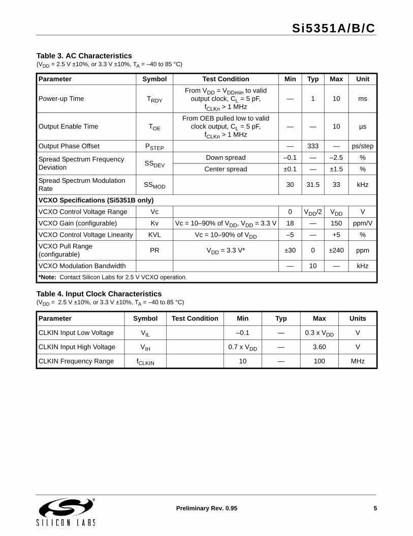
Table 3. AC Characteristics(VDD = 2.5 V ±10%, or 3.3 V ±10%, TA = –40 to 85 °C)
Parameter Symbol Test Condition Min Typ Max Unit
Power-up Time TRDY
From VDD = VDDmin to valid output clock, CL = 5 pF,
fCLKn > 1 MHz— 1 10 ms
Output Enable Time TOE
From OEB pulled low to valid clock output, CL = 5 pF,
fCLKn > 1 MHz— — 10 µs
Output Phase Offset PSTEP — 333 — ps/step
Spread Spectrum Frequency Deviation
SSDEVDown spread –0.1 — –2.5 %
Center spread ±0.1 — ±1.5 %
Spread Spectrum Modulation Rate
SSMOD 30 31.5 33 kHz
VCXO Specifications (Si5351B only)
VCXO Control Voltage Range Vc 0 VDD/2 VDD V
VCXO Gain (configurable) Kv Vc = 10–90% of VDD, VDD = 3.3 V 18 — 150 ppm/V
VCXO Control Voltage Linearity KVL Vc = 10–90% of VDD –5 — +5 %
VCXO Pull Range (configurable)
PR VDD = 3.3 V* ±30 0 ±240 ppm
VCXO Modulation Bandwidth — 10 — kHz
*Note: Contact Silicon Labs for 2.5 V VCXO operation.
Table 4. Input Clock Characteristics(VDD = 2.5 V ±10%, or 3.3 V ±10%, TA = –40 to 85 °C)
Parameter Symbol Test Condition Min Typ Max Units
CLKIN Input Low Voltage VIL –0.1 — 0.3 x VDD V
CLKIN Input High Voltage VIH 0.7 x VDD — 3.60 V
CLKIN Frequency Range fCLKIN 10 — 100 MHz

Si5351A/B/C
6 Preliminary Rev. 0.95
Table 5. Output Clock Characteristics(VDD = 2.5 V ±10%, or 3.3 V ±10%, TA = –40 to 85 °C)
Parameter Symbol Test Condition Min Typ Max Units
Frequency Range FCLK 0.008 — 160 MHz
Load Capacitance CL — 5 15 pF
Duty Cycle DCMeasured at VDD/2,
fCLK = 50 MHz45 50 55 %
Rise/Fall Timetr 20%–80%, CL = 5 pF,
Drive Strength = 8 mA
0.5 1 1.5 ns
tf 0.5 1 1.5 ns
Output High Voltage VOHCL = 5 pF
VDD – 0.6 — — V
Output Low Voltage VOL — — 0.6 V
Period Jitter JPERMeasured over 10k cycles
— 35 100 ps pk-pk
Period Jitter VCXO JPER_VCXO — 60 110 ps pk-pk
Cycle-to-Cycle Jitter JCC
Measured over 10k cycles
— 30 90 ps pk
Cycle-to-Cycle Jitter VCXO
JCC_VCXO — 50 95 ps pk
RMS Phase Jitter JRMS12 kHz–20 MHz
— 3.5 11 ps rms
RMS Phase Jitter VCXO JRMS_VCXO — 8.5 18.5 ps rms
Table 6. Crystal Requirements1,2
Parameter Symbol Min Typ Max Unit
Crystal Frequency fXTAL 25 — 27 MHz
Load Capacitance CL 6 — 12 pF
Equivalent Series Resistance rESR — — 150
Crystal Max Drive Level dL — — 100 µW
Notes:1. Crystals which require load capacitances of 6, 8, or 10 pF should use the device’s internal load capacitance for
optimum performance. See register 183 bits 7:6. A crystal with a 12 pF load capacitance requirement should use a combination of the internal 10 pF load capacitors in addition to external 2 pF load capacitors.
2. Refer to “AN551: Crystal Selection Guide” for more details.

Si5351A/B/C
Preliminary Rev. 0.95 7
Table 7. I2C Specifications (SCL,SDA)1
Parameter Symbol Test Condition Standard Mode
100 kbpsFast Mode
400 kbpsUnit
Min Max Min Max
LOW Level Input Voltage
VILI2C –0.5 0.3 x VDDI2
C –0.5 0.3 x VDDI2C
2 V
HIGH Level Input Voltage
VIHI2C0.7 x VDDI2
C3.63 0.7 x VDDI2C
2 3.63 V
Hysteresis of Schmitt Trigger Inputs
VHYS — — 0.1 — V
LOW Level Output Voltage (open drain or open collector) at 3 mA Sink Current
VOLI2C2
VDDI2C2 = 2.5/3.3 V 0 0.4 0 0.4 V
VDDI2C2 = 1.8 V — — 0 0.2 x VDDI2C V
Input Current III2C –10 10 –10 10 µA
Capacitance for Each I/O Pin
CII2C VIN = –0.1 to VDDI2C — 4 — 4 pF
I2C Bus Timeout
TTO Timeout Enabled 25 35 25 35 ms
Notes:1. Refer to NXP’s UM10204 I2C-bus specification and user manual, revision 03, for further details, go to:
www.nxp.com/acrobat_download/usermanuals/UM10204_3.pdf.2. Only I2C pullup voltages (VDDI2C) of 2.25 to 3.63 V are supported.
Table 8. Thermal Characteristics
Parameter Symbol Test Condition Package Value Unit
Thermal Resistance Junction to Ambient
JA Still Air
10-MSOP 131 °C/W
24-QSOP 80 °C/W
20-QFN 51 °C/W
Thermal Resistance Junction to Case
JC Still Air
10-MSOP 43 °C/W
24-QSOP 31 °C/W
20-QFN 16 °C/W

Si5351A/B/C
8 Preliminary Rev. 0.95
Table 9. Absolute Maximum Ratings1
Parameter Symbol Test Condition Value Unit
DC Supply Voltage VDD_max –0.5 to 3.8 V
Input Voltage
VIN_CLKIN CLKIN, SCL, SDA –0.5 to 3.8 V
VIN_VC VC –0.5 to (VDD+0.3) V
VIN_XA/B Pins XA, XB –0.5 to 1.3 V V
Junction Temperature TJ –55 to 150 °C
Soldering Temperature (Pb-free profile)2
TPEAK 260 °C
Soldering Temperature Time at TPEAK (Pb-free profile)2
TP 20–40 Sec
Notes:1. Permanent device damage may occur if the absolute maximum ratings are exceeded. Functional operation should be
restricted to the conditions as specified in the operational sections of this data sheet. Exposure to absolute maximum rating conditions for extended periods may affect device reliability.
2. The device is compliant with JEDEC J-STD-020.

Si5351A/B/C
Preliminary Rev. 0.95 9
2. Detailed Block Diagrams
Figure 1. Block Diagrams of 3-Output and 8-Output Si5351A Devices
PLLB
PLLA
SDA
SCL
OSCXA
XB
VDDO
R0
R1
CLK0
CLK1
R2 CLK2
MultiSynth 0
MultiSynth 1
MultiSynth 2
VDD
GND 10-MSOP
Si5351A 3-Output
R0
R1
CLK0
CLK1
VDDOA
R2
R3
CLK2
CLK3
VDDOB
R4
R5
CLK4
CLK5
VDDOC
R6
R7
CLK6
CLK7
VDDOD
MultiSynth 0
MultiSynth 1
MultiSynth 2
MultiSynth 3
MultiSynth 4
MultiSynth 5
MultiSynth 6
MultiSynth 7
VDD
GND 20-QFN, 24-QSOP
SCL
A0
SDA
Control Logic
OEB
SSEN
I2C Interface
Si5351A 8-Output
I2C Interface
PLLB
PLLA
OSCXA
XB
Si5351A/B/C
10 Preliminary Rev. 0.95
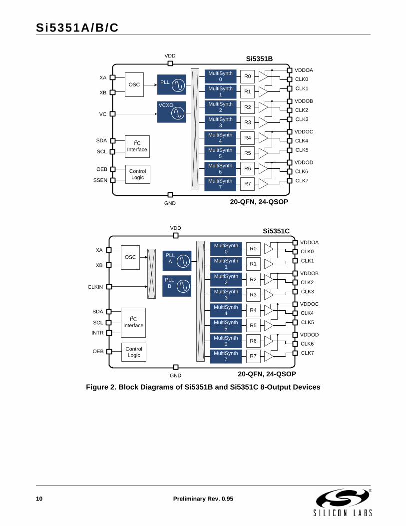
Figure 2. Block Diagrams of Si5351B and Si5351C 8-Output Devices
OSCXA
XB
PLL
VCXO
R0
R1
CLK0
CLK1
VDDOA
R2
R3
CLK2
CLK3
VDDOB
R4
R5
CLK4
CLK5
VDDOC
R6
R7
CLK6
CLK7
VDDOD
MultiSynth 0
MultiSynth 1
MultiSynth 2
MultiSynth 3
MultiSynth 4
MultiSynth 5
MultiSynth 6
MultiSynth 7
VC
VDD
GND
Si5351B
SCL
SDA
Control Logic
OEB
SSEN
I2C Interface
20-QFN, 24-QSOP
R0
R1
CLK0
CLK1
VDDOA
R2
R3
CLK2
CLK3
VDDOB
R4
R5
CLK4
CLK5
VDDOC
R6
R7
CLK6
CLK7
VDDOD
MultiSynth 0
MultiSynth 1
MultiSynth 2
MultiSynth 3
MultiSynth 4
MultiSynth 5
MultiSynth 6
MultiSynth 7
VDD
GND
Si5351C
PLLA
PLLB
XA
XB
OSC
CLKIN
SCL
SDA
Control Logic
INTR
OEB
I2C Interface
20-QFN, 24-QSOP

Si5351A/B/C
Preliminary Rev. 0.95 11
3. Functional Description
The Si5351 is a versatile I2C programmable clock generator that is ideally suited for replacing crystals, crystaloscillators, VCXOs, PLLs, and buffers. A block diagram showing the general architecture of the Si5351 is shown inFigure 3. The device consists of an input stage, two synthesis stages, and an output stage.
The input stage accepts an external crystal (XTAL), a clock input (CLKIN), or a control voltage input (VC)depending on the version of the device (A/B/C). The first stage of synthesis multiplies the input frequencies to anhigh-frequency intermediate clock, while the second stage of synthesis uses high resolution MultiSynth fractionaldividers to generate the desired output frequencies. Additional integer division is provided at the output stage forgenerating output frequencies as low as 8 kHz. Crosspoint switches at each of the synthesis stages allows totalflexibility in routing any of the inputs to any of the outputs.
Because of this high resolution and flexible synthesis architecture, the Si5351 is capable of generatingsynchronous or free-running non-integer related clock frequencies at each of its outputs, enabling one device tosynthesize clocks for multiple clock domains in a design.
Figure 3. Si5351 Block Diagram
3.1. Input Stage3.1.1. Crystal Inputs (XA, XB)
The Si5351 uses a fixed-frequency standard AT-cut crystal as a reference to the internal oscillator. The output ofthe oscillator can be used to provide a free-running reference to one or both of the PLLs for generatingasynchronous clocks. The output frequency of the oscillator will operate at the crystal frequency, either 25 MHz or27 MHz. The crystal is also used as a reference to the VCXO to help maintain its frequency accuracy.
Internal load capacitors (CL) are provided to eliminate the need for external components when connecting a crystalto the Si5351. Options for internal load capacitors are 6, 8, or 10 pF. Crystals with alternate load capacitancerequirements are supported using additional external load capacitors as shown in Figure 4. Refer to applicationnote AN551 for crystal recommendations.
Figure 4. External XTAL with Optional Load Capacitors
Input Stage
Synthesis Stage 1
PLL B (VCXO)
PLL A(SSC)
VC VCXO
XA
XB
OSCXTAL
CLKIN Div
Multi Synth
0
Multi Synth
1
Multi Synth
2
Multi Synth
3
Multi Synth
4
Multi Synth
5
Multi Synth
6
Multi Synth
7
Synthesis Stage 2
R0
R1
R2
R3
R4
R5
R6
R7
Output Stage
CLK0
CLK1
VDDOA
CLK2
CLK3
VDDOB
CLK4
CLK5
VDDOC
CLK6
CLK7
VDDOD
XA
XB
Selectable internal load capacitors
6 pF, 8 pF, 10 pF
CL CL
CL
Optional Additional external
load capacitors (< 2 pF)
CL
Si5351A/B/C
12 Preliminary Rev. 0.95
3.1.2. External Clock Input (CLKIN)
The external clock input is used as a clock reference for the PLLs when generating synchronous clock outputs.CLKIN can accept any frequency from 10 to 100 MHz. A divider at the input stage limits the PLL input frequency to30 MHz.
3.1.3. Voltage Control Input (VC)
The VCXO architecture of the Si5350B eliminates the need for an external pullable crystal. Only a standard, low-cost, fixed-frequency (25 or 27 MHz) AT-cut crystal is required.
The tuning range of the VCXO is configurable allowing for a wide variety of applications. Key advantages of theVCXO design in the Si5351 include high linearity, a wide operating range (linear from 10 to 90% of VDD), andreliable startup and operation. Refer to Table 3 on page 5 for VCXO specification details.
A unique feature of the Si5351B is its ability to generate multiple output frequencies controlled by the same controlvoltage applied to the VC pin. This replaces multiple PLLs or VCXOs that would normally be locked to the samereference. An example is illustrated in Figure 9 on page 15.
3.2. Synthesis StagesThe Si5351 uses two stages of synthesis to generate its final output clocks. The first stage uses PLLs to multiplythe lower frequency input references to a high-frequency intermediate clock. The second stage uses high-resolution MultiSynth fractional dividers to generate frequencies in the range of 1 MHz to 100 MHz. It is alsopossible to generate two unique frequencies up to 160 MHz on two or more of the outputs.
A crosspoint switch at the input of the first stage allows each of the PLLs to lock to the CLKIN or the XTAL input.This allows each of the PLLs to lock to a different source for generating independent free-running and synchronousclocks. Alternatively, both PLLs could lock to the same source. The crosspoint switch at the input of the secondstage allows any of the MultiSynth dividers to connect to PLLA or PLLB. This flexible synthesis architecture allowsany of the outputs to generate synchronous or non-synchronous clocks, with spread spectrum or without spreadspectrum, and with the flexibility of generating non-integer related clock frequencies at each output.
Since the VCXO already generates a high-frequency intermediate clock, it is fed directly into the second stage ofsynthesis. The MultiSynth high-resolution dividers synthesize the VCXO center frequency to any frequency in therange of ~391 kHz to 160 MHz. The center frequency is then controlled (or pulled) by the VC input. An interestingfeature of the Si5351 is that the VCXO output can be routed to more than one MultiSynth divider. This creates aVCXO with multiple output frequencies controlled from one VC input as shown in Figure 5.
Frequencies down to 8 kHz can be generated by applying the R divider at the output of the Multisynth (seeFigure 5 below).
Figure 5. Using the Si5351 as a Multi-Output VCXO
3.3. Output StageAn additional level of division (R) is available at the output stage for generating clocks as low as 8 kHz. All outputdrivers generate CMOS level outputs with separate output voltage supply pins (VDDOx) allowing a different voltagesignal level (1.8, 2.5, or 3.3 V) at each of the four 2-output banks.
CLK0
VC
Multi Synth
2
CLK1
CLK2
Additional MultiSynths can be “linked” to the
VCXO to generate additional clock
frequencies
XA XB
OSC
VCXOMulti Synth
1
Multi Synth
0
Control Voltage
Fixed Frequency Crystal (non-pullable)
The clock frequency generated from CLK0 is
controlled by the VC input
R2
R1
R0

Si5351A/B/C
Preliminary Rev. 0.95 13
3.4. Spread SpectrumSpread spectrum can be enabled on any of the clock outputs that use PLLA as its reference. Spread spectrum isuseful for reducing electromagnetic interference (EMI). Enabling spread spectrum on an output clock modulates itsfrequency, which effectively reduces the overall amplitude of its radiated energy. See “AN554: Si5350/51 PCBLayout Guide” for details. Note that spread spectrum is not available on clocks synchronized to PLLB or to theVCXO.
The Si5351 supports several levels of spread spectrum allowing the designer to chose an ideal compromisebetween system performance and EMI compliance.
Figure 6. Available Spread Spectrum Profiles
3.5. Control Pins (OEB, SSEN)The Si5351 offers control pins for enabling/disabling clock outputs and spread spectrum.
3.5.1. Output Enable (OEB)
The output enable pin allows enabling or disabling outputs clocks. Output clocks are enabled when the OEB pin isheld low, and disabled when pulled high. When disabled, the output state is configurable as disabled high, disabledlow, or disabled in high-impedance.
The output enable control circuitry ensures glitchless operation by starting the output clock cycle on the first leadingedge after OEB is pulled low. When OEB is pulled high, the clock is allowed to complete its full clock cycle beforegoing into a disabled state.
3.5.2. Spread Spectrum Enable (SSEN)—Si5351A and Si5351B only
This control pin allows disabling the spread spectrum feature for all outputs that were configured with spreadspectrum enabled. Hold SSEN low to disable spread spectrum. The SSEN pin provides a convenient method ofevaluating the effect of using spread spectrum clocks during EMI compliance testing.
fc
Reduced Amplitude and EMI
Down Spread
fc
Reduced Amplitude and EMI
Center Spread
fcNo Spread Spectrum
Center FrequencyAmplitude

Si5351A/B/C
14 Preliminary Rev. 0.95
4. I2C Interface
Many of the functions and features of the Si5351 are controlled by reading and writing to the RAM space using theI2C interface. The following is a list of the common features that are controllable through the I2C interface. Asummary of register functions is shown in Section 7.
Read Status IndicatorsLoss of signal (LOS) for the CLKIN inputLoss of lock (LOL) for PLLA and PLLB
Configuration of multiplication and divider values for the PLLs, MultiSynth dividers
Configuration of the Spread Spectrum profile (down or center spread, modulation percentage)
Control of the cross point switch selection for each of the PLLs and MultiSynth dividers
Set output clock optionsEnable/disable for each clock outputInvert/non-invert for each clock output
Output divider values (2n, n=1.. 7)Output state when disabled (stop hi, stop low, Hi-Z) Output phase offset
The I2C interface operates in slave mode with 7-bit addressing and can operate in Standard-Mode (100 kbps) orFast-Mode (400 kbps) and supports burst data transfer with auto address increments.
The I2C bus consists of a bidirectional serial data line (SDA) and a serial clock input (SCL) as shown in Figure 7.Both the SDA and SCL pins must be connected to the VDD supply via an external pull-up as recommended by theI2C specification.
Figure 7. I2C and Control Signals
The 7-bit device (slave) address of the Si5351 consist of a 6-bit fixed address plus a user selectable LSB bit asshown in Figure 8. The LSB bit is selectable as 0 or 1 using the optional A0 pin which is useful for applications thatrequire more than one Si5351 on a single I2C bus.
Figure 8. Si5351 I2C Slave Address
Data is transferred MSB first in 8-bit words as specified by the I2C specification. A write command consists of a 7-bit device (slave) address + a write bit, an 8-bit register address, and 8 bits of data as shown in Figure 9. A writeburst operation is also shown where every additional data word is written using to an auto-incremented address.
SCL
VDD
SDAI2C Bus
INTR
A0I2C Address Select:Pull-up to VDD (A0 = 1)
Pull-down to GND (A0 = 0)
Si5351>1k >1k
4.7 k
Slave Address 1 1 0 0 0 0 0/1
A0
0123456

Si5351A/B/C
Preliminary Rev. 0.95 15
Figure 9. I2C Write Operation
A read operation is performed in two stages. A data write is used to set the register address, then a data read isperformed to retrieve the data from the set address. A read burst operation is also supported. This is shown inFigure 10.
Figure 10. I2C Read Operation
AC and DC electrical specifications for the SCL and SDA pins are shown in Table 7. The timing specifications andtiming diagram for the I2C bus is compatible with the I2C-Bus Standard. SDA timeout is supported for compatibilitywith SMBus interfaces.
1 – Read0 – WriteA – Acknowledge (SDA LOW)N – Not Acknowledge (SDA HIGH)S – START conditionP – STOP condition
From slave to master
From master to slave
Write Operation – Single Byte
S 0 A Reg Addr [7:0]Slv Addr [6:0] A Data [7:0] PA
Write Operation - Burst (Auto Address Increment)
Reg Addr +1
S 0 A Reg Addr [7:0]Slv Addr [6:0] A Data [7:0] A Data [7:0] PA
1 – Read0 – WriteA – Acknowledge (SDA LOW)N – Not Acknowledge (SDA HIGH)S – START conditionP – STOP condition
From slave to master
From master to slave
Read Operation – Single Byte
S 0 A Reg Addr [7:0]Slv Addr [6:0] A P
Read Operation - Burst (Auto Address Increment)
Reg Addr +1
S 1 ASlv Addr [6:0] Data [7:0] PN
S 0 A Reg Addr [7:0]Slv Addr [6:0] A P
S 1 ASlv Addr [6:0] Data [7:0] A PNData [7:0]
Si5351A/B/C
16 Preliminary Rev. 0.95
5. Configuring the Si5351
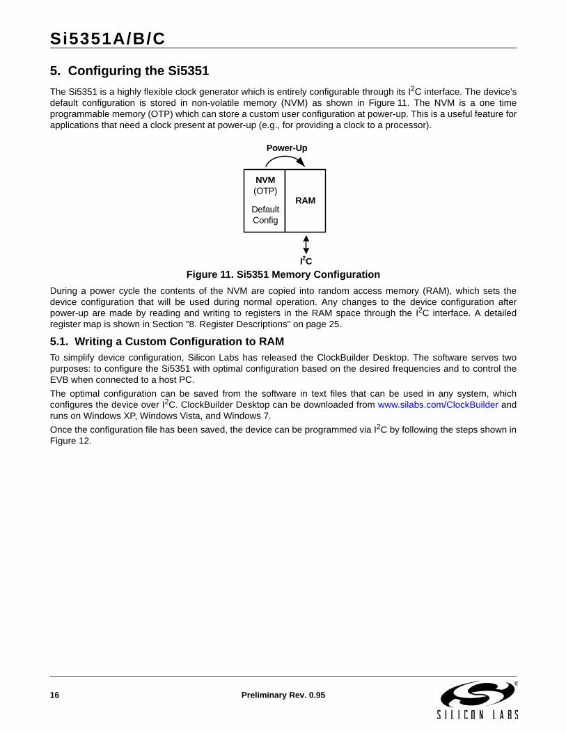
The Si5351 is a highly flexible clock generator which is entirely configurable through its I2C interface. The device’sdefault configuration is stored in non-volatile memory (NVM) as shown in Figure 11. The NVM is a one timeprogrammable memory (OTP) which can store a custom user configuration at power-up. This is a useful feature forapplications that need a clock present at power-up (e.g., for providing a clock to a processor).
Figure 11. Si5351 Memory Configuration
During a power cycle the contents of the NVM are copied into random access memory (RAM), which sets thedevice configuration that will be used during normal operation. Any changes to the device configuration afterpower-up are made by reading and writing to registers in the RAM space through the I2C interface. A detailedregister map is shown in Section "8. Register Descriptions" on page 25.
5.1. Writing a Custom Configuration to RAMTo simplify device configuration, Silicon Labs has released the ClockBuilder Desktop. The software serves twopurposes: to configure the Si5351 with optimal configuration based on the desired frequencies and to control theEVB when connected to a host PC.
The optimal configuration can be saved from the software in text files that can be used in any system, whichconfigures the device over I2C. ClockBuilder Desktop can be downloaded from www.silabs.com/ClockBuilder andruns on Windows XP, Windows Vista, and Windows 7.
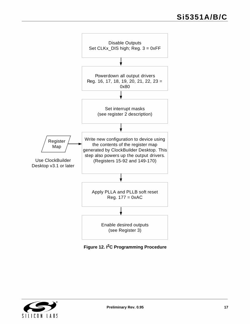
Once the configuration file has been saved, the device can be programmed via I2C by following the steps shown inFigure 12.
Power-Up
I2C
RAM
NVM (OTP)
Default Config
Si5351A/B/C
Preliminary Rev. 0.95 17
Figure 12. I2C Programming Procedure
Disable OutputsSet CLKx_DIS high; Reg. 3 = 0xFF
Powerdown all output driversReg. 16, 17, 18, 19, 20, 21, 22, 23 =
0x80
Set interrupt masks(see register 2 description)
Write new configuration to device using the contents of the register map
generated by ClockBuilder Desktop. This step also powers up the output drivers.
(Registers 15-92 and 149-170)
Apply PLLA and PLLB soft resetReg. 177 = 0xAC
Enable desired outputs(see Register 3)
Use ClockBuilder Desktop v3.1 or later
RegisterMap

Si5351A/B/C
18 Preliminary Rev. 0.95
5.2. Si5351 Application ExamplesThe Si5351 is a versatile clock generator which serves a wide variety of applications. The following examples showhow it can be used to replace crystals, crystal oscillators, VCXOs, and PLLs.
5.3. Replacing Crystals and Crystal OscillatorsUsing an inexpensive external crystal, the Si5351A can generate up to 8 different free-running clock frequenciesfor replacing crystals and crystal oscillators. A 3-output version packaged in a small 10-MSOP is also available forapplications that require fewer clocks. An example is shown in Figure 13.
Figure 13. Using the Si5351A to Replace Multiple Crystals, Crystal Oscillators, and PLLs
48 MHz USB Controller
28.322 MHz
125 MHz
Video/Audio Processor
74.25/1.001 MHz
24.576 MHz
OSC
XA
XB
CLK0
CLK1
CLK2
CLK3
CLK4
CLK5
PLL
Multi Synth
0
Multi Synth
1
Multi Synth
2
74.25 MHz
27 MHz
Si5351A
Multi Synth
3
Multi Synth
4
Multi Synth
5
Multi Synth
7
HDMI Port
Ethernet PHY
Multi Synth
6
22.5792 MHzCLK6
33.3333 MHzCLK7CPU
Note: Si5351A replaces crystals, XOs, and PLLs.

Si5351A/B/C
Preliminary Rev. 0.95 19
5.4. Replacing Crystals, Crystal Oscillators, and VCXOsThe Si5351B combines free-running clock generation and a VCXO in a single package for cost sensitive videoapplications. An example is shown in Figure 14.
Figure 14. Using the Si5351B to Replace Crystals, Crystal Oscillators, VCXOs, and PLLs
5.5. Replacing Crystals, Crystal Oscillators, and PLLsThe Si5350C generates synchronous clocks for applications that require a fully integrated PLL instead of a VCXO.Because of its dual PLL architecture, the Si5351C is capable of generating both synchronous and free-runningclocks. An example is shown in Figure 15.
Figure 15. Using the Si5351C to Replace Crystals, Crystal Oscillators, and PLLs
Ethernet PHY
USB Controller
HDMI Port
28.322 MHz
48 MHz
125 MHz
Video/Audio Processor
74.25/1.001 MHz
24.576 MHz
OSC
XA
XB
CLK0
CLK1
CLK2
CLK3
CLK4
CLK5
PLL
VCXO
Multi Synth
0
Multi Synth
1
Multi Synth
2
74.25 MHz
VC
27 MHz
Si5351B
Multi Synth
3
Multi Synth
4
Multi Synth
5
Free-running Clocks
Synchronous Clocks
Note: FBW = 10 kHz
Ethernet PHY
USB Controller
HDMI Port
28.322 MHz
48 MHz
125 MHz
Video/Audio Processor
74.25/1.001 MHz
24.576 MHz
OSC
XA
XB
CLK0
CLK1
CLK2
CLK3
CLK4
CLK5
PLL
PLL
Multi Synth
0
Multi Synth
1
Multi Synth
2
74.25 MHz
CLKIN
25 MHz
Si5351C
Multi Synth
3
Multi Synth
4
Multi Synth
5
54 MHz
Free-running Clocks
Synchronous Clocks

Si5351A/B/C
20 Preliminary Rev. 0.95
5.6. Replacing a Crystal with a ClockThe Si5351 can be driven with a clock signal through the XA input pin.
Figure 16. Si5351 Driven by a Clock Signal
5.7. HCSL Compatible OutputsThe Si5351 can be configured to support HCSL compatible swing when the VDDO of the output pair of interest isset to 2.5 V (i.e., VDDOA must be 2.5 V when using CLK0/1; VDDOB must be 2.5 V for CLK2/3 and so on).
The circuit in the figure below must be applied to each of the two clocks used, and one of the clocks in the pairmust also be inverted to generate a differential pair. See register setting CLKx_INV.
Figure 17. Si5350C Output is HCSL Compatible
Multi Synth
N
Multi Synth
0
Multi Synth
1
PLLB
PLLAXA
XB
OSC
VIN = 1 VPP
25/27 MHz
Note: Float the XB input while driving the XA input with a clock
0.1 µF
Multi Synth
N
Multi Synth
0
Multi Synth
1
PLLB
PLLA
OSC
Note: The complementary -180 degree out of phase output clock is generated using the INV function
R1
511
240 R2
ZO = 70
0
HCSLCLKIN
R1
511
240 R2
ZO = 70
0

Si5351A/B/C
Preliminary Rev. 0.95 21
6. Design Considerations
The Si5351 is a self-contained clock generator that requires very few external components. The following generalguidelines are recommended to ensure optimum performance. Refer to “AN554: Si5350/51 PCB Layout Guide” foradditional layout recommendations.
6.1. Power Supply Decoupling/FilteringThe Si5351 has built-in power supply filtering circuitry and extensive internal Low Drop Out (LDO) voltageregulators to help minimize the number of external bypass components. All that is recommended is one 0.1 µFdecoupling capacitor per power supply pin. This capacitor should be mounted as close to the VDD and VDDOxpins as possible without using vias.
6.2. Power Supply SequencingThe VDD and VDDOx (i.e., VDDO0, VDDO1, VDDO2, VDDO3) power supply pins have been separated to allowflexibility in output signal levels. If a minimum output-to-output skew is important, then all VDDOx must be appliedbefore VDD. Unused VDDOx pins should be tied to VDD.
6.3. External CrystalThe external crystal should be mounted as close to the pins as possible using short PCB traces. The XA and XBtraces should be kept away from other high-speed signal traces. See “AN551: Crystal Selection Guide” for moredetails.
6.4. External Crystal Load CapacitorsThe Si5351 provides the option of using internal and external crystal load capacitors. If internal load capacitance isinsufficient, capacitors of value < 2 pF may be used to increased equivalent load capacitance. If external loadcapacitors are used, they should be placed as close to the XA/XB pads as possible. See AN554 for more details.
6.5. Unused PinsUnused voltage control pin should be tied to GND.
Unused CLKIN pin should be tied to GND.
Unused XA/XB pins should be left floating. Refer to "5.6. Replacing a Crystal with a Clock" on page 20 when usingXA as a clock input pin.
Unused output pins (CLK0–CLK7) should be left floating.
Unused VDDOx pins should be tied to VDD.

Si5351A/B/C
22 Preliminary Rev. 0.95
6.6. Trace CharacteristicsThe Si5351A/B/C features various output current drives ranging from 2 to 8 mA (default). It is recommended toconfigure the trace characteristics as shown in Figure 18 when an output drive setting of 8 mA is used.
Figure 18. Recommended Trace Characteristics with 8 mA Drive Strength Setting
Note: Jitter is only specified at 6 and 8 mA drive strength.
ZO = 85 ohms
Length = No Restrictions
CLK
(Optional resistor for EMI management)
R = 0 ohms

Si5351A/B/C
Preliminary Rev. 0.95 23
7. Register Map Summary
The following is a summary of the register map used to read status, control, and configure the Si5351.
Register 7 6 5 4 3 2 1 0
0 SYS_INIT LOL_B LOL_A LOS REVID[1:0]
1 SYSCAL_STKY
LOS_B_STKY
LOL_A_STKY
LOS_STKY
2 SYSCAL_MASK
LOS_B_MASK
LOL_A _MASK
LOS_MASK
3 CLK7_EN CLK6_EN CLK5_EN CLK4_EN CLK3_EN CLK2_EN CLK1_EN CLK0_EN
4–8 Reserved
9 OEB_CLK7 OEB_CLK6 OEB_CLK5 OEB_CLK4 OEB_CLK3 OEB_CLK2 OEB_CLK1 OEB_CLK0
10–14 Reserved
15 0 0 0 0 PLLB_SRC PLLA_SRC 0 0
16 CLK0_PDN MS0_INT MS0_SRC CLK0_INV CLK0_SRC[1:0] CLK0_IDRV[1:0]
17 CLK1_PDN MS1_INT MS1_SRC CLK1_INV CLK1_SRC[1:0] CLK1_IDRV[1:0]
18 CLK2_PDN MS2_INT MS2_SRC CLK2_INV CLK2_SRC[1:0] CLK2_IDRV[1:0]
19 CLK3_PDN MS3_INT MS3_SRC CLK3_INV CLK3_SRC[1:0] CLK3_IDRV[1:0]
20 CLK4_PDN MS4_INT MS4_SRC CLK4_INV CLK4_SRC[1:0] CLK4_IDRV[1:0]
21 CLK5_PDN MS5_INT MS5_SRC CLK5_INV CLK5_SRC[1:0] CLK5_IDRV[1:0]
22 CLK6_PDN FBA_INT MS6_SRC CLK6_INV CLK6_SRC[1:0] CLK6_IDRV[1:0]
23 CLK7_PDN FBB_INT MS6_SRC CLK7_INV CLK7_SRC[1:0] CLK7_IDRV[1:0]
24 CLK3_DIS_STATE CLK2_DIS_STATE CLK1_DIS_STATE CLK0_DIS_STATE
25 CLK7_DIS_STATE CLK6_DIS_STATE CLK5_DIS_STATE CLK4_DIS_STATE
26–41 PLL, MultiSynth, and output clock delay offset Configuration Registers. Use ClockBuilder Desktop Software to Determine These Register Values.
42 MS0_P3[15:8]
43 MS0_P3[7:0]
44 R0_DIV[2:0] MS0_P1[17:16]
45 MS0_P1[15:8]
46 MS0_P1[7:0]
47 MS0_P3[19:16] MS0_P2[19:16]
48 MS0_P2[15:8]
49 MS0_P2[7:0]
50 MS1_P3[15:8]
51 MS1_P3[7:0]
52 R1_DIV[2:0] MS1_P1[17:16]
53 MS1_P1[15:8]
54 MS1_P1[7:0]
55 MS1_P3[19:16] MS1_P2[19:16]
56 MS1_P2[15:8]
57 MS1_P2[7:0]
58 MS2_P3[15:8]
59 MS2_P3[7:0]
60 R2_DIV[2:0] MS2_P1[17:16]
61 MS2_P1[15:8]
62 MS2_P1[7:0]
63 MS2_P3[19:16] MS2_P2[19:16]
64 MS2_P2[15:8]
65 MS2_P2[7:0]

Si5351A/B/C
24 Preliminary Rev. 0.95
66 MS3_P3[15:8]
67 MS3_P3[7:0]
68 R3_DIV[2:0] MS3_P1[17:16]
69 MS3_P1[15:8]
70 MS3_P1[7:0]
71 MS3_P3[19:16] MS3_P2[19:16]
72 MS3_P2[15:8]
73 MS3_P2[7:0]
74 MS4_P3[15:8]
75 MS4_P3[7:0]
76 R4_DIV[2:0] MS4_P1[17:16]
77 MS4_P1[15:8]
78 MS4_P1[7:0]
79 MS4_P3[19:16] MS4_P2[19:16]
80 MS4_P2[15:8]
81 MS4_P2[7:0]
82 MS5_P3[15:8]
83 MS5_P3[7:0]
84 R5_DIV[2:0] MS5_P1[17:16]
85 MS5_P1[15:8]
86 MS5_P1[7:0]
87 MS5_P3[19:16] MS5_P2[19:16]
88 MS5_P2[15:8]
89 MS5_P2[7:0]
90 MS6_P1[7:0]
91 MS7_P1[7:0]
92 R7_DIV[2:0] R6_DIV[2:0]
93–164 PLL, MultiSynth, and output clock delay offset Configuration Registers. Use ClockBuilder Desktop Software to Determine These Register Values.
165 CLK0_PHOFF[7:0]
166 CLK1_PHOFF[7:0]
167 CLK2_PHOFF[7:0]
168 CLK3_PHOFF[7:0]
189 CLK4_PHOFF[7:0]
170 CLK5_PHOFF[7:0]
173–176 Reserved
177 PLLB_RST PLLA_RST
178–182 Reserved
183 XTAL_CL
184–255 Reserved
Register 7 6 5 4 3 2 1 0

Si5351A/B/C
Preliminary Rev. 0.95 25
8. Register Descriptions
Reset value = 0000 0000
Register 0. Device Status
Bit D7 D6 D5 D4 D3 D2 D1 D0
Name SYS_INIT LOL_B LOL_A LOS REVID[1:0]
Type R R R R R R R
Bit Name Function
7 SYS_INIT System Initialization Status.
During power up the device copies the content of the NVM into RAM and performs a system initialization. The device is not operational until initialization is complete. It is not recom-mended to read or write registers in RAM through the I2C interface until initialization is com-plete. An interrupt will be triggered (INTR pin = 0, Si5351C only) during the system initialization period.0: System initialization is complete. Device is ready.1: Device is in system initialization mode.
6 LOL_B PLLB Loss Of Lock Status.
Si5351A/C only. PLLB will operate in a locked state when it has a valid reference from CLKIN or XTAL. A loss of lock will occur if the frequency of the reference clock forces the PLL to operate outside of its lock range as specified in Table 3, or if the reference clock fails to meet the minimum requirements of a valid input signal as specified in Table 4. An interrupt will be triggered (INTR pin = 0, Si5351C) during a LOL condition.0: PLL B is locked.1: PLL B is unlocked. When the device is in this state it will trigger an interrupt causing the INTR pin to go low (Si5351C only).
5 LOL_A PLL A Loss Of Lock Status.
PLL A will operate in a locked state when it has a valid reference from CLKIN or XTAL. A loss of lock will occur if the frequency of the reference clock forces the PLL to operate outside of its lock range as specified in Table 3, or if the reference clock fails to meet the minimum requirements of a valid input signal as specified in Table 4. An interrupt will be triggered (INTR pin = 0, Si5351C only) during a LOL condition.0: PLL A is operating normally.1: PLL A is unlocked. When the device is in this state it will trigger an interrupt causing the INTR pin to go low (Si5351C only).
4 LOS CLKIN Loss Of Signal (Si5351C Only).
A loss of signal status indicates if the reference clock fails to meet the minimum requirements of a valid input signal as specified in Table 4. An interrupt will be triggered (INTR pin = 0, Si5351C only) during a LOS condition.0: Valid clock signal at the CLKIN pin.1: Loss of signal detected at the CLKIN pin.
3:2 Reserved Leave as default.
1:0 REVID[1:0] Revision ID. Device revision number. Set at the factory.
Si5351A/B/C
26 Preliminary Rev. 0.95
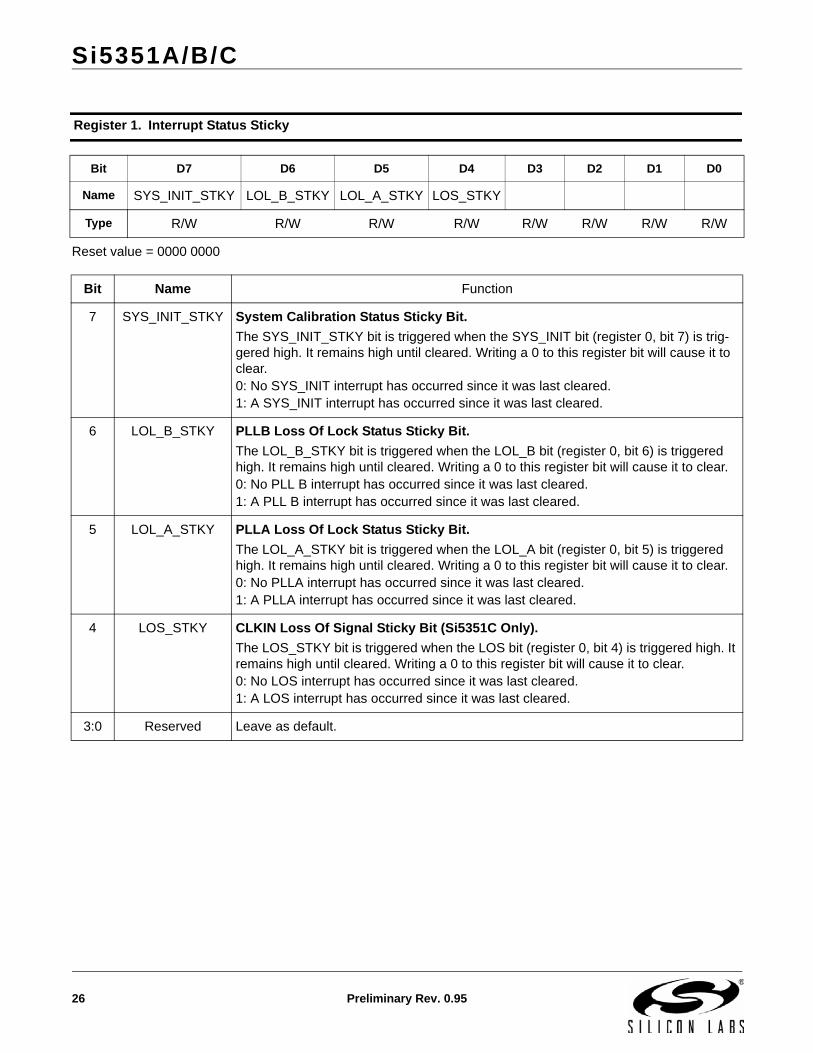
Reset value = 0000 0000
Register 1. Interrupt Status Sticky
Bit D7 D6 D5 D4 D3 D2 D1 D0
Name SYS_INIT_STKY LOL_B_STKY LOL_A_STKY LOS_STKY
Type R/W R/W R/W R/W R/W R/W R/W R/W
Bit Name Function
7 SYS_INIT_STKY System Calibration Status Sticky Bit.
The SYS_INIT_STKY bit is triggered when the SYS_INIT bit (register 0, bit 7) is trig-gered high. It remains high until cleared. Writing a 0 to this register bit will cause it to clear. 0: No SYS_INIT interrupt has occurred since it was last cleared.1: A SYS_INIT interrupt has occurred since it was last cleared.
6 LOL_B_STKY PLLB Loss Of Lock Status Sticky Bit.
The LOL_B_STKY bit is triggered when the LOL_B bit (register 0, bit 6) is triggered high. It remains high until cleared. Writing a 0 to this register bit will cause it to clear. 0: No PLL B interrupt has occurred since it was last cleared.1: A PLL B interrupt has occurred since it was last cleared.
5 LOL_A_STKY PLLA Loss Of Lock Status Sticky Bit.
The LOL_A_STKY bit is triggered when the LOL_A bit (register 0, bit 5) is triggered high. It remains high until cleared. Writing a 0 to this register bit will cause it to clear. 0: No PLLA interrupt has occurred since it was last cleared.1: A PLLA interrupt has occurred since it was last cleared.
4 LOS_STKY CLKIN Loss Of Signal Sticky Bit (Si5351C Only).
The LOS_STKY bit is triggered when the LOS bit (register 0, bit 4) is triggered high. It remains high until cleared. Writing a 0 to this register bit will cause it to clear. 0: No LOS interrupt has occurred since it was last cleared.1: A LOS interrupt has occurred since it was last cleared.
3:0 Reserved Leave as default.

Si5351A/B/C
Preliminary Rev. 0.95 27
Reset value = 0000 0000
Register 2. Interrupt Status Mask
Bit D7 D6 D5 D4 D3 D2 D1 D0
Name SYS_INIT_MASK LOL_B_MASK LOL_A_MASK LOS_MASK
Type R/W R/W R/W R/W R/W R/W R/W R/W
Bit Name Function
7 SYS_INIT_MASK System Initialization Status Mask.
Use this mask bit to prevent the INTR pin (Si5351C only) from going low when SYS_INIT is asserted. 0: Do not mask the SYS_INIT interrupt.1: Mask the SYS_INIT interrupt.
6 LOL_B_MASK PLLB Loss Of Lock Status Mask.
Use this mask bit to prevent the INTR pin (Si5351C only) from going low when LOL_B is asserted. 0: Do not mask the LOL_B interrupt. 1: Mask the LOL_B interrupt.
5 LOL_A_MASK PLL A Loss Of Lock Status Mask.
Use this mask bit to prevent the INTR pin (Si5351C only) from going low when LOL_A is asserted.0: Do not mask the LOL_A interrupt.1: Mask the LOL_A interrupt.
4 LOS_MASK CLKIN Loss Of Signal Mask (Si5351C Only).
Use this mask bit to prevent the INTR pin (Si5351C only) from going low when LOS is asserted.0: Do not mask the LOS interrupt. 1: Mask the LOS interrupt.
3:0 Reserved Leave as default.
Si5351A/B/C
28 Preliminary Rev. 0.95
Reset value = 0000 0000
Reset value = 0000 0000
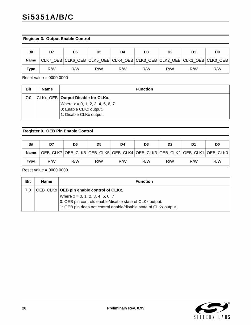
Register 3. Output Enable Control
Bit D7 D6 D5 D4 D3 D2 D1 D0
Name CLK7_OEB CLK6_OEB CLK5_OEB CLK4_OEB CLK3_OEB CLK2_OEB CLK1_OEB CLK0_OEB
Type R/W R/W R/W R/W R/W R/W R/W R/W
Bit Name Function
7:0 CLKx_OEB Output Disable for CLKx.
Where x = 0, 1, 2, 3, 4, 5, 6, 70: Enable CLKx output.1: Disable CLKx output.
Register 9. OEB Pin Enable Control
Bit D7 D6 D5 D4 D3 D2 D1 D0
Name OEB_CLK7 OEB_CLK6 OEB_CLK5 OEB_CLK4 OEB_CLK3 OEB_CLK2 OEB_CLK1 OEB_CLK0
Type R/W R/W R/W R/W R/W R/W R/W R/W
Bit Name Function
7:0 OEB_CLKx OEB pin enable control of CLKx.
Where x = 0, 1, 2, 3, 4, 5, 6, 70: OEB pin controls enable/disable state of CLKx output.1: OEB pin does not control enable/disable state of CLKx output.
Si5351A/B/C
Preliminary Rev. 0.95 29
Reset value = 0000 0000
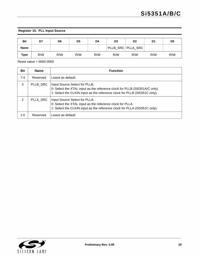
Register 15. PLL Input Source
Bit D7 D6 D5 D4 D3 D2 D1 D0
Name PLLB_SRC PLLA_SRC
Type R/W R/W R/W R/W R/W R/W R/W R/W
Bit Name Function
7:4 Reserved Leave as default.
3 PLLB_SRC Input Source Select for PLLB.0: Select the XTAL input as the reference clock for PLLB (Si5351A/C only).1: Select the CLKIN input as the reference clock for PLLB (Si5351C only).
2 PLLA_SRC Input Source Select for PLLA.0: Select the XTAL input as the reference clock for PLLA.1: Select the CLKIN input as the reference clock for PLLA (Si5351C only).
1:0 Reserved Leave as default.
Si5351A/B/C
30 Preliminary Rev. 0.95
Reset value = 0000 0000
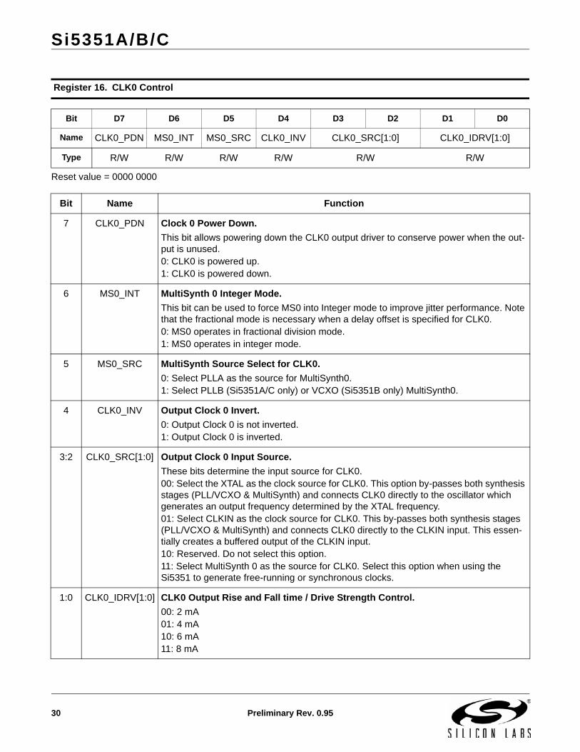
Register 16. CLK0 Control
Bit D7 D6 D5 D4 D3 D2 D1 D0
Name CLK0_PDN MS0_INT MS0_SRC CLK0_INV CLK0_SRC[1:0] CLK0_IDRV[1:0]
Type R/W R/W R/W R/W R/W R/W
Bit Name Function
7 CLK0_PDN Clock 0 Power Down.
This bit allows powering down the CLK0 output driver to conserve power when the out-put is unused.0: CLK0 is powered up.1: CLK0 is powered down.
6 MS0_INT MultiSynth 0 Integer Mode.
This bit can be used to force MS0 into Integer mode to improve jitter performance. Note that the fractional mode is necessary when a delay offset is specified for CLK0.0: MS0 operates in fractional division mode.1: MS0 operates in integer mode.
5 MS0_SRC MultiSynth Source Select for CLK0.
0: Select PLLA as the source for MultiSynth0.1: Select PLLB (Si5351A/C only) or VCXO (Si5351B only) MultiSynth0.
4 CLK0_INV Output Clock 0 Invert.
0: Output Clock 0 is not inverted.1: Output Clock 0 is inverted.
3:2 CLK0_SRC[1:0] Output Clock 0 Input Source.
These bits determine the input source for CLK0.00: Select the XTAL as the clock source for CLK0. This option by-passes both synthesis stages (PLL/VCXO & MultiSynth) and connects CLK0 directly to the oscillator which generates an output frequency determined by the XTAL frequency.01: Select CLKIN as the clock source for CLK0. This by-passes both synthesis stages (PLL/VCXO & MultiSynth) and connects CLK0 directly to the CLKIN input. This essen-tially creates a buffered output of the CLKIN input. 10: Reserved. Do not select this option.11: Select MultiSynth 0 as the source for CLK0. Select this option when using the Si5351 to generate free-running or synchronous clocks.
1:0 CLK0_IDRV[1:0] CLK0 Output Rise and Fall time / Drive Strength Control.
00: 2 mA01: 4 mA10: 6 mA11: 8 mA
Si5351A/B/C
Preliminary Rev. 0.95 31
Reset value = 0000 0000
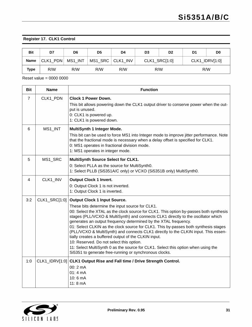
Register 17. CLK1 Control
Bit D7 D6 D5 D4 D3 D2 D1 D0
Name CLK1_PDN MS1_INT MS1_SRC CLK1_INV CLK1_SRC[1:0] CLK1_IDRV[1:0]
Type R/W R/W R/W R/W R/W R/W
Bit Name Function
7 CLK1_PDN Clock 1 Power Down.
This bit allows powering down the CLK1 output driver to conserve power when the out-put is unused.0: CLK1 is powered up. 1: CLK1 is powered down.
6 MS1_INT MultiSynth 1 Integer Mode.
This bit can be used to force MS1 into Integer mode to improve jitter performance. Note that the fractional mode is necessary when a delay offset is specified for CLK1.0: MS1 operates in fractional division mode.1: MS1 operates in integer mode.
5 MS1_SRC MultiSynth Source Select for CLK1.
0: Select PLLA as the source for MultiSynth0.1: Select PLLB (Si5351A/C only) or VCXO (Si5351B only) MultiSynth0.
4 CLK1_INV Output Clock 1 Invert.
0: Output Clock 1 is not inverted.1: Output Clock 1 is inverted.
3:2 CLK1_SRC[1:0] Output Clock 1 Input Source.
These bits determine the input source for CLK1.00: Select the XTAL as the clock source for CLK1. This option by-passes both synthesis stages (PLL/VCXO & MultiSynth) and connects CLK1 directly to the oscillator which generates an output frequency determined by the XTAL frequency.01: Select CLKIN as the clock source for CLK1. This by-passes both synthesis stages (PLL/VCXO & MultiSynth) and connects CLK1 directly to the CLKIN input. This essen-tially creates a buffered output of the CLKIN input.10: Reserved. Do not select this option.11: Select MultiSynth 0 as the source for CLK1. Select this option when using the Si5351 to generate free-running or synchronous clocks.
1:0 CLK1_IDRV[1:0] CLK1 Output Rise and Fall time / Drive Strength Control.
00: 2 mA01: 4 mA10: 6 mA11: 8 mA
Si5351A/B/C
32 Preliminary Rev. 0.95
Reset value = 0000 0000
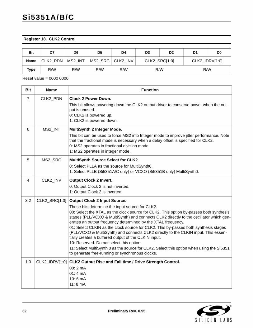
Register 18. CLK2 Control
Bit D7 D6 D5 D4 D3 D2 D1 D0
Name CLK2_PDN MS2_INT MS2_SRC CLK2_INV CLK2_SRC[1:0] CLK2_IDRV[1:0]
Type R/W R/W R/W R/W R/W R/W
Bit Name Function
7 CLK2_PDN Clock 2 Power Down.
This bit allows powering down the CLK2 output driver to conserve power when the out-put is unused.0: CLK2 is powered up. 1: CLK2 is powered down.
6 MS2_INT MultiSynth 2 Integer Mode.
This bit can be used to force MS2 into Integer mode to improve jitter performance. Note that the fractional mode is necessary when a delay offset is specified for CLK2.0: MS2 operates in fractional division mode.1: MS2 operates in integer mode.
5 MS2_SRC MultiSynth Source Select for CLK2.
0: Select PLLA as the source for MultiSynth0.1: Select PLLB (Si5351A/C only) or VCXO (Si5351B only) MultiSynth0.
4 CLK2_INV Output Clock 2 Invert.
0: Output Clock 2 is not inverted.1: Output Clock 2 is inverted.
3:2 CLK2_SRC[1:0] Output Clock 2 Input Source.
These bits determine the input source for CLK2.00: Select the XTAL as the clock source for CLK2. This option by-passes both synthesis stages (PLL/VCXO & MultiSynth) and connects CLK2 directly to the oscillator which gen-erates an output frequency determined by the XTAL frequency.01: Select CLKIN as the clock source for CLK2. This by-passes both synthesis stages (PLL/VCXO & MultiSynth) and connects CLK2 directly to the CLKIN input. This essen-tially creates a buffered output of the CLKIN input.10: Reserved. Do not select this option.11: Select MultiSynth 0 as the source for CLK2. Select this option when using the Si5351 to generate free-running or synchronous clocks.
1:0 CLK2_IDRV[1:0] CLK2 Output Rise and Fall time / Drive Strength Control.
00: 2 mA01: 4 mA10: 6 mA11: 8 mA

Si5351A/B/C
Preliminary Rev. 0.95 33
Reset value = 0000 0000
Register 19. CLK3 Control
Bit D7 D6 D5 D4 D3 D2 D1 D0
Name CLK3_PDN MS3_INT MS3_SRC CLK3_INV CLK3_SRC[1:0] CLK3_IDRV[1:0]
Type R/W R/W R/W R/W R/W R/W
Bit Name Function
7 CLK3_PDN Clock 3 Power Down.
This bit allows powering down the CLK3 output driver to conserve power when the out-put is unused.0: CLK3 is powered up. 1: CLK3 is powered down.
6 MS3_INT MultiSynth 3 Integer Mode.
This bit can be used to force MS3 into Integer mode to improve jitter performance. Note that the fractional mode is necessary when a delay offset is specified for CLK3.0: MS3 operates in fractional division mode.1: MS3 operates in integer mode.
5 MS3_SRC MultiSynth Source Select for CLK3.
0: Select PLLA as the source for MultiSynth0.1: Select PLLB (Si5351A/C only) or VCXO (Si5351B only) MultiSynth0.
4 CLK3_INV Output Clock 3 Invert.
0: Output Clock 3 is not inverted.1: Output Clock 3 is inverted.
3:2 CLK3_SRC[1:0] Output Clock 3 Input Source.
These bits determine the input source for CLK3.
1:0 CLK3_IDRV[1:0] CLK3 Output Rise and Fall time / Drive Strength Control.
00: 2 mA01: 4 mA10: 6 mA11: 8 mA

Si5351A/B/C
34 Preliminary Rev. 0.95
Reset value = 0000 0000
Register 20. CLK4 Control
Bit D7 D6 D5 D4 D3 D2 D1 D0
Name CLK4_PDN MS4_INT MS4_SRC CLK4_INV CLK4_SRC[1:0] CLK4_IDRV[1:0]
Type R/W R/W R/W R/W R/W R/W
Bit Name Function
7 CLK4_PDN Clock 4 Power Down.
This bit allows powering down the CLK4 output driver to conserve power when the out-put is unused.0: CLK4 is powered up. 1: CLK4 is powered down.
6 MS4_INT MultiSynth 4 Integer Mode.
This bit can be used to force MS4 into Integer mode to improve jitter performance. Note that the fractional mode is necessary when a delay offset is specified for CLK4.0: MS4 operates in fractional division mode. 1: MS4 operates in integer mode.
5 MS4_SRC MultiSynth Source Select for CLK4.
0: Select PLLA as the source for MultiSynth0.1: Select PLLB (Si5351A/C only) or VCXO (Si5351B only) MultiSynth0.
4 CLK4_INV Output Clock 4 Invert.
0: Output Clock 4 is not inverted.1: Output Clock 4 is inverted.
3:2 CLK4_SRC[1:0] Output Clock 4 Input Source.
These bits determine the input source for CLK4.00: Select the XTAL as the clock source for CLK4. This option by-passes both synthe-sis stages (PLL/VCXO & MultiSynth) and connects CLK4 directly to the oscillator which generates an output frequency determined by the XTAL frequency.01: Select CLKIN as the clock source for CLK4. This by-passes both synthesis stages (PLL/VCXO & MultiSynth) and connects CLK4 directly to the CLKIN input. This essen-tially creates a buffered output of the CLKIN input. 10: Reserved. Do not select this option.11: Select MultiSynth 0 as the source for CLK4. Select this option when using the Si5351 to generate free-running or synchronous clocks.
1:0 CLK4_IDRV[1:0] CLK4 Output Rise and Fall time / Drive Strength Control.
00: 2 mA01: 4 mA10: 6 mA11: 8 mA
Si5351A/B/C
Preliminary Rev. 0.95 35
Reset value = 0000 0000
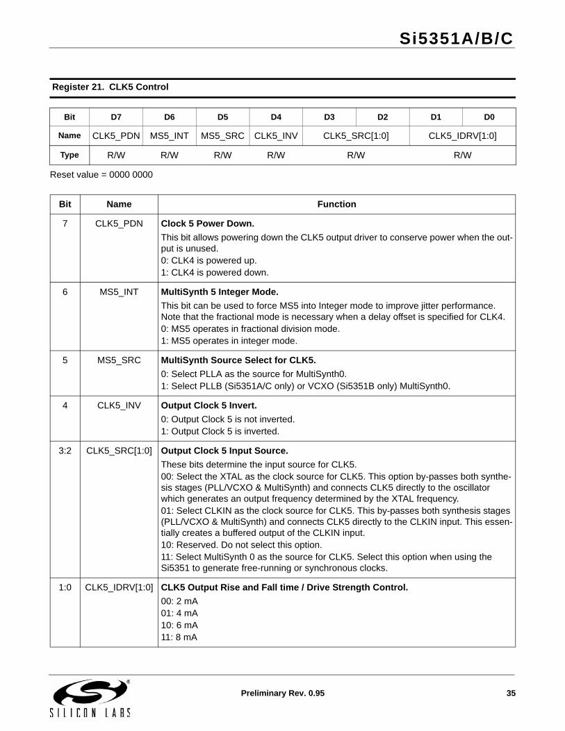
Register 21. CLK5 Control
Bit D7 D6 D5 D4 D3 D2 D1 D0
Name CLK5_PDN MS5_INT MS5_SRC CLK5_INV CLK5_SRC[1:0] CLK5_IDRV[1:0]
Type R/W R/W R/W R/W R/W R/W
Bit Name Function
7 CLK5_PDN Clock 5 Power Down.
This bit allows powering down the CLK5 output driver to conserve power when the out-put is unused.0: CLK4 is powered up. 1: CLK4 is powered down.
6 MS5_INT MultiSynth 5 Integer Mode.
This bit can be used to force MS5 into Integer mode to improve jitter performance. Note that the fractional mode is necessary when a delay offset is specified for CLK4.0: MS5 operates in fractional division mode. 1: MS5 operates in integer mode.
5 MS5_SRC MultiSynth Source Select for CLK5.
0: Select PLLA as the source for MultiSynth0.1: Select PLLB (Si5351A/C only) or VCXO (Si5351B only) MultiSynth0.
4 CLK5_INV Output Clock 5 Invert.
0: Output Clock 5 is not inverted.1: Output Clock 5 is inverted.
3:2 CLK5_SRC[1:0] Output Clock 5 Input Source.
These bits determine the input source for CLK5.00: Select the XTAL as the clock source for CLK5. This option by-passes both synthe-sis stages (PLL/VCXO & MultiSynth) and connects CLK5 directly to the oscillator which generates an output frequency determined by the XTAL frequency.01: Select CLKIN as the clock source for CLK5. This by-passes both synthesis stages (PLL/VCXO & MultiSynth) and connects CLK5 directly to the CLKIN input. This essen-tially creates a buffered output of the CLKIN input. 10: Reserved. Do not select this option.11: Select MultiSynth 0 as the source for CLK5. Select this option when using the Si5351 to generate free-running or synchronous clocks.
1:0 CLK5_IDRV[1:0] CLK5 Output Rise and Fall time / Drive Strength Control.
00: 2 mA01: 4 mA10: 6 mA11: 8 mA

Si5351A/B/C
36 Preliminary Rev. 0.95
Reset value = 0000 0000
Register 22. CLK6 Control
Bit D7 D6 D5 D4 D3 D2 D1 D0
Name CLK6_PDN FBA_INT MS6_SRC CLK6_INV CLK6_SRC[1:0] CLK6_IDRV[1:0]
Type R/W R/W R/W R/W R/W R/W
Bit Name Function
7 CLK6_PDN Clock 7 Power Down.
This bit allows powering down the CLK6 output driver to conserve power when the out-put is unused.0: CLK6 is powered up. 1: CLK6 is powered down.
6 FBA_INT FBA MultiSynth Integer Mode.
Set this bit according to ClockBuilder Desktop generated register map file.
5 MS6_SRC MultiSynth Source Select for CLK6.
0: Select PLLA as the source for MultiSynth0.1: Select PLLB (Si5351A/C only) or VCXO (Si5351B only) MultiSynth0.
4 CLK6_INV Output Clock 6 Invert.
0: Output Clock 6 is not inverted.1: Output Clock 6 is inverted.
3:2 CLK6_SRC[1:0] Output Clock 0 Input Source.
These bits determine the input source for CLK6.00: Select the XTAL as the clock source for CLK6. This option by-passes both synthe-sis stages (PLL/VCXO & MultiSynth) and connects CLK6 directly to the oscillator which generates an output frequency determined by the XTAL frequency.01: Select CLKIN as the clock source for CLK6. This by-passes both synthesis stages (PLL/VCXO & MultiSynth) and connects CLK6 directly to the CLKIN input. This essen-tially creates a buffered output of the CLKIN input. 10: Reserved. Do not select this option.11: Select MultiSynth 0 as the source for CLK6. Select this option when using the Si5351 to generate free-running or synchronous clocks.
1:0 CLK6_IDRV[1:0] CLK6 Output Rise and Fall time / Drive Strength Control.
00: 2 mA01: 4 mA10: 6 mA11: 8 mA
Si5351A/B/C
Preliminary Rev. 0.95 37
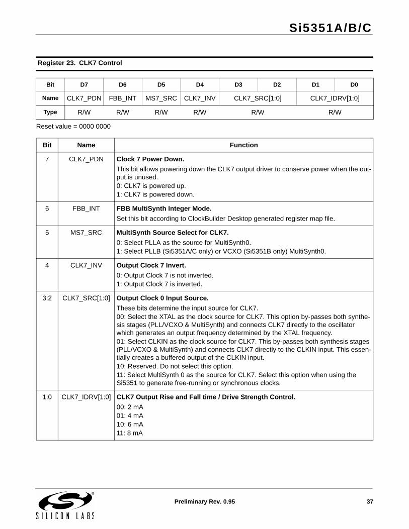
Reset value = 0000 0000
Register 23. CLK7 Control
Bit D7 D6 D5 D4 D3 D2 D1 D0
Name CLK7_PDN FBB_INT MS7_SRC CLK7_INV CLK7_SRC[1:0] CLK7_IDRV[1:0]
Type R/W R/W R/W R/W R/W R/W
Bit Name Function
7 CLK7_PDN Clock 7 Power Down.
This bit allows powering down the CLK7 output driver to conserve power when the out-put is unused.0: CLK7 is powered up. 1: CLK7 is powered down.
6 FBB_INT FBB MultiSynth Integer Mode.
Set this bit according to ClockBuilder Desktop generated register map file.
5 MS7_SRC MultiSynth Source Select for CLK7.
0: Select PLLA as the source for MultiSynth0.1: Select PLLB (Si5351A/C only) or VCXO (Si5351B only) MultiSynth0.
4 CLK7_INV Output Clock 7 Invert.
0: Output Clock 7 is not inverted.1: Output Clock 7 is inverted.
3:2 CLK7_SRC[1:0] Output Clock 0 Input Source.
These bits determine the input source for CLK7.00: Select the XTAL as the clock source for CLK7. This option by-passes both synthe-sis stages (PLL/VCXO & MultiSynth) and connects CLK7 directly to the oscillator which generates an output frequency determined by the XTAL frequency.01: Select CLKIN as the clock source for CLK7. This by-passes both synthesis stages (PLL/VCXO & MultiSynth) and connects CLK7 directly to the CLKIN input. This essen-tially creates a buffered output of the CLKIN input. 10: Reserved. Do not select this option.11: Select MultiSynth 0 as the source for CLK7. Select this option when using the Si5351 to generate free-running or synchronous clocks.
1:0 CLK7_IDRV[1:0] CLK7 Output Rise and Fall time / Drive Strength Control.
00: 2 mA01: 4 mA10: 6 mA11: 8 mA
Si5351A/B/C
38 Preliminary Rev. 0.95
Reset value = 0000 0000
Reset value = 0000 0000
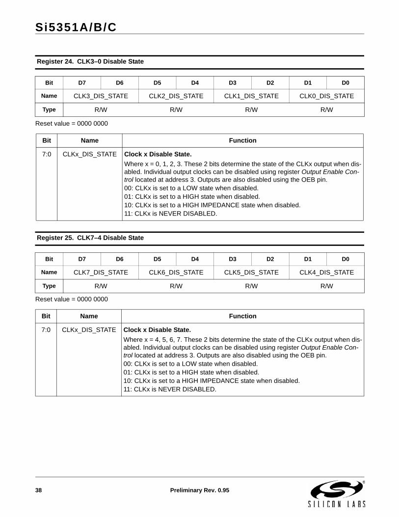
Register 24. CLK3–0 Disable State
Bit D7 D6 D5 D4 D3 D2 D1 D0
Name CLK3_DIS_STATE CLK2_DIS_STATE CLK1_DIS_STATE CLK0_DIS_STATE
Type R/W R/W R/W R/W
Bit Name Function
7:0 CLKx_DIS_STATE Clock x Disable State.
Where x = 0, 1, 2, 3. These 2 bits determine the state of the CLKx output when dis-abled. Individual output clocks can be disabled using register Output Enable Con-trol located at address 3. Outputs are also disabled using the OEB pin. 00: CLKx is set to a LOW state when disabled.01: CLKx is set to a HIGH state when disabled.10: CLKx is set to a HIGH IMPEDANCE state when disabled.11: CLKx is NEVER DISABLED.
Register 25. CLK7–4 Disable State
Bit D7 D6 D5 D4 D3 D2 D1 D0
Name CLK7_DIS_STATE CLK6_DIS_STATE CLK5_DIS_STATE CLK4_DIS_STATE
Type R/W R/W R/W R/W
Bit Name Function
7:0 CLKx_DIS_STATE Clock x Disable State.
Where x = 4, 5, 6, 7. These 2 bits determine the state of the CLKx output when dis-abled. Individual output clocks can be disabled using register Output Enable Con-trol located at address 3. Outputs are also disabled using the OEB pin. 00: CLKx is set to a LOW state when disabled.01: CLKx is set to a HIGH state when disabled.10: CLKx is set to a HIGH IMPEDANCE state when disabled.11: CLKx is NEVER DISABLED.
Si5351A/B/C
Preliminary Rev. 0.95 39
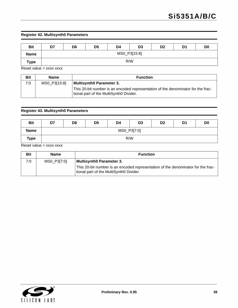
Reset value = xxxx xxxx
Reset value = xxxx xxxx
Register 42. Multisynth0 Parameters
Bit D7 D6 D5 D4 D3 D2 D1 D0
Name MS0_P3[15:8]
Type R/W
Bit Name Function
7:0 MS0_P3[15:8] Multisynth0 Parameter 3.
This 20-bit number is an encoded representation of the denominator for the frac-tional part of the MultiSynth0 Divider.
Register 43. Multisynth0 Parameters
Bit D7 D6 D5 D4 D3 D2 D1 D0
Name MS0_P3[7:0]
Type R/W
Bit Name Function
7:0 MS0_P3[7:0] Multisynth0 Parameter 3.
This 20-bit number is an encoded representation of the denominator for the frac-tional part of the MultiSynth0 Divider.

Si5351A/B/C
40 Preliminary Rev. 0.95
Reset value = xxxx xxxx
Reset value = xxxx xxxx
Register 44. Multisynth0 Parameters
Bit D7 D6 D5 D4 D3 D2 D1 D0
Name R0_DIV[2:0] MS0_P1[17:16]
Type R/W R/W R/W R/W R/W
Bit Name Function
7 Unused
6:4 R0_DIV[2:0] R0 Output Divider.
000b: Divide by 1001b: Divide by 2010b: Divide by 4011b: Divide by 8100b: Divide by 16101b: Divide by 32110b: Divide by 64111b: Divide by 128
3:2 Reserved
1:0 MS0_P1[17:16] Multisynth0 Parameter 1.
This 18-bit number is an encoded representation of the integer part of the MultiSynth0 divider.
Register 45. Multisynth0 Parameters
Bit D7 D6 D5 D4 D3 D2 D1 D0
Name MS0_P1[15:8]
Type R/W
Bit Name Function
7:0 MS0_P1[15:8] Multisynth0 Parameter 1.
This 18-bit number is an encoded representation of the integer part of the MultiSynth1 divider.

Si5351A/B/C
Preliminary Rev. 0.95 41
Reset value = xxxx xxxx
Reset value = xxxx xxxx
Reset value = xxxx xxxx
Register 46. Multisynth0 Parameters
Bit D7 D6 D5 D4 D3 D2 D1 D0
Name MS0_P1[7:0]
Type R/W
Bit Name Function
7:0 MS0_P1[7:0] Multisynth0 Parameter 1.
This 18-bit number is an encoded representation of the integer part of the MultiSynth1 divider.
Register 47. Multisynth0 Parameters
Bit D7 D6 D5 D4 D3 D2 D1 D0
Name MS0_P3[19:16] MS0_P2[19:16]
Type R/W R/W
Bit Name Function
7:4 MS0_P3[19:16] Multisynth0 Parameter 3.
This 20-bit number is an encoded representation of the denominator for the frac-tional part of the MultiSynth0 Divider
3:0 MS0_P2[19:16] Multisynth0 Parameter 2.
This 20-bit number is an encoded representation of the numerator for the fractional part of the MultiSynth1 Divider.
Register 48. Multisynth0 Parameters
Bit D7 D6 D5 D4 D3 D2 D1 D0
Name MS0_P2[15:8]
Type R/W
Bit Name Function
7:0 MS0_P2[15:8] Multisynth0 Parameter 2.
This 20-bit number is an encoded representation of the numerator for the fractional part of the MultiSynth1 Divider.

Si5351A/B/C
42 Preliminary Rev. 0.95
Reset value = xxxx xxxx
Reset value = xxxx xxxx
Reset value = xxxx xxxx
Register 49. Multisynth0 Parameters
Bit D7 D6 D5 D4 D3 D2 D1 D0
Name MS0_P2[7:0]
Type R/W
Bit Name Function
7:0 MS0_P2[7:0] Multisynth0 Parameter 2.
This 20-bit number is an encoded representation of the numerator for the fractional part of the MultiSynth1 Divider.
Register 50. Multisynth1 Parameters
Bit D7 D6 D5 D4 D3 D2 D1 D0
Name MS1_P3[15:8]
Type R/W
Bit Name Function
7:0 MS1_P3[15:8] Multisynth1 Parameter 3.
This 20-bit number is an encoded representation of the denominator for the frac-tional part of the MultiSynth1 Divider.
Register 51. Multisynth1 Parameters
Bit D7 D6 D5 D4 D3 D2 D1 D0
Name MS1_P3[7:0]
Type R/W
Bit Name Function
7:0 MS1_P3[7:0] Multisynth1 Parameter 3.
This 20-bit number is an encoded representation of the denominator for the frac-tional part of the MultiSynth1 Divider.

Si5351A/B/C
Preliminary Rev. 0.95 43
Reset value = xxxx xxxx
Reset value = xxxx xxxx
Register 52. Multisynth1 Parameters
Bit D7 D6 D5 D4 D3 D2 D1 D0
Name R1_DIV[2:0] MS1_P1[17:16]
Type R/W R/W R/W R/W R/W
Bit Name Function
7 Unused
6:4 R1_DIV[2:0] R1 Output Divider.
000b: Divide by 1001b: Divide by 2010b: Divide by 4011b: Divide by 8100b: Divide by 16101b: Divide by 32110b: Divide by 64111b: Divide by 128
3:2 Reserved
1:0 MS1_P1[17:16] Multisynth1 Parameter 1.
This 18-bit number is an encoded representation of the integer part of the MultiSynth1 divider.
Register 53. Multisynth1 Parameters
Bit D7 D6 D5 D4 D3 D2 D1 D0
Name MS1_P1[15:8]
Type R/W
Bit Name Function
7:0 MS1_P1[15:8] Multisynth1 Parameter 1.
This 18-bit number is an encoded representation of the integer part of the MultiSynth1 divider.

Si5351A/B/C
44 Preliminary Rev. 0.95
Reset value = xxxx xxxx
Reset value = xxxx xxxx
Reset value = xxxx xxxx
Register 54. Multisynth1 Parameters
Bit D7 D6 D5 D4 D3 D2 D1 D0
Name MS1_P1[7:0]
Type R/W
Bit Name Function
7:0 MS1_P1[7:0] Multisynth1 Parameter 1.
This 18-bit number is an encoded representation of the integer part of the MultiSynth1 divider.
Register 55. Multisynth1 Parameters
Bit D7 D6 D5 D4 D3 D2 D1 D0
Name MS1_P3[19:16] MS1_P2[19:16]
Type R/W R/W
Bit Name Function
7:4 MS1_P3[19:16] Multisynth1 Parameter 3.
This 20-bit number is an encoded representation of the denominator for the frac-tional part of the Multisynth1 Divider
3:0 MS1_P2[19:16] Multisynth1 Parameter 2.
This 20-bit number is an encoded representation of the numerator for the fractional part of the MultiSynth1 Divider.
Register 56. Multisynth1 Parameters
Bit D7 D6 D5 D4 D3 D2 D1 D0
Name MS1_P2[15:8]
Type R/W
Bit Name Function
7:0 MS1_P2[15:8] Multisynth1 Parameter 2.
This 20-bit number is an encoded representation of the numerator for the fractional part of the MultiSynth1 divider.
Si5351A/B/C
Preliminary Rev. 0.95 45
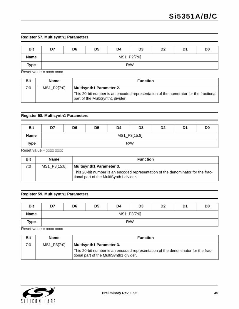
Reset value = xxxx xxxx
Reset value = xxxx xxxx
Reset value = xxxx xxxx
Register 57. Multisynth1 Parameters
Bit D7 D6 D5 D4 D3 D2 D1 D0
Name MS1_P2[7:0]
Type R/W
Bit Name Function
7:0 MS1_P2[7:0] Multisynth1 Parameter 2.
This 20-bit number is an encoded representation of the numerator for the fractional part of the MultiSynth1 divider.
Register 58. Multisynth1 Parameters
Bit D7 D6 D5 D4 D3 D2 D1 D0
Name MS1_P3[15:8]
Type R/W
Bit Name Function
7:0 MS1_P3[15:8] Multisynth1 Parameter 3.
This 20-bit number is an encoded representation of the denominator for the frac-tional part of the MultiSynth1 divider.
Register 59. Multisynth1 Parameters
Bit D7 D6 D5 D4 D3 D2 D1 D0
Name MS1_P3[7:0]
Type R/W
Bit Name Function
7:0 MS1_P3[7:0] Multisynth1 Parameter 3.
This 20-bit number is an encoded representation of the denominator for the frac-tional part of the MultiSynth1 divider.

Si5351A/B/C
46 Preliminary Rev. 0.95
Reset value = xxxx xxxx
Reset value = xxxx xxxx
Register 60. Multisynth2 Parameters
Bit D7 D6 D5 D4 D3 D2 D1 D0
Name R2_DIV[2:0] MS2_P1[17:16]
Type R/W R/W R/W R/W R/W
Bit Name Function
7 Unused
6:4 R2_DIV[2:0] R2 Output Divider.
000b: Divide by 1001b: Divide by 2010b: Divide by 4011b: Divide by 8100b: Divide by 16101b: Divide by 32110b: Divide by 64111b: Divide by 128
3:2 Reserved
1:0 MS2_P1[17:16] Multisynth2 Parameter 1.
This 18-bit number is an encoded representation of the integer part of the Multisynth2 divider.
Register 61. Multisynth2 Parameters
Bit D7 D6 D5 D4 D3 D2 D1 D0
Name MS2_P1[15:8]
Type R/W
Bit Name Function
7:0 MS2_P1[15:8] Multisynth2 Parameter 1.
This 18-bit number is an encoded representation of the integer part of the Multisynth2 divider.
Si5351A/B/C
Preliminary Rev. 0.95 47
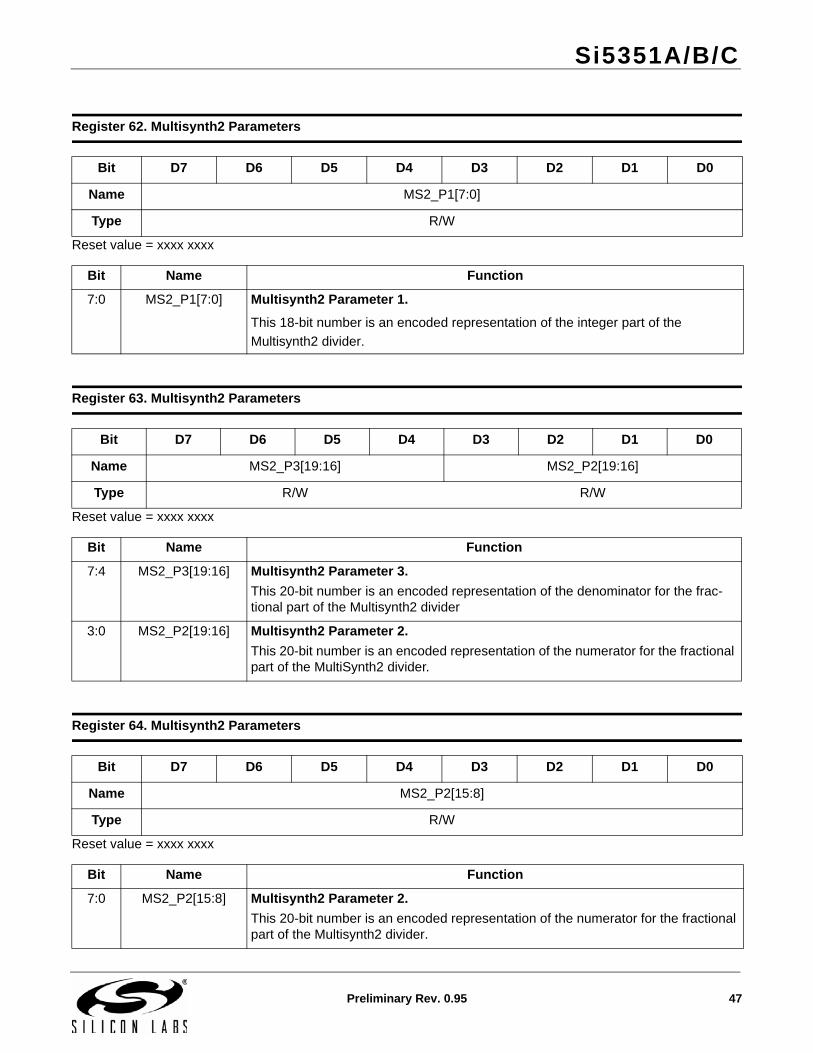
Reset value = xxxx xxxx
Reset value = xxxx xxxx
Reset value = xxxx xxxx
Register 62. Multisynth2 Parameters
Bit D7 D6 D5 D4 D3 D2 D1 D0
Name MS2_P1[7:0]
Type R/W
Bit Name Function
7:0 MS2_P1[7:0] Multisynth2 Parameter 1.
This 18-bit number is an encoded representation of the integer part of the
Multisynth2 divider.
Register 63. Multisynth2 Parameters
Bit D7 D6 D5 D4 D3 D2 D1 D0
Name MS2_P3[19:16] MS2_P2[19:16]
Type R/W R/W
Bit Name Function
7:4 MS2_P3[19:16] Multisynth2 Parameter 3.
This 20-bit number is an encoded representation of the denominator for the frac-tional part of the Multisynth2 divider
3:0 MS2_P2[19:16] Multisynth2 Parameter 2.
This 20-bit number is an encoded representation of the numerator for the fractional part of the MultiSynth2 divider.
Register 64. Multisynth2 Parameters
Bit D7 D6 D5 D4 D3 D2 D1 D0
Name MS2_P2[15:8]
Type R/W
Bit Name Function
7:0 MS2_P2[15:8] Multisynth2 Parameter 2.
This 20-bit number is an encoded representation of the numerator for the fractional part of the Multisynth2 divider.

Si5351A/B/C
48 Preliminary Rev. 0.95
Reset value = xxxx xxxx
Reset value = xxxx xxxx
Reset value = xxxx xxxx
Register 65. Multisynth2 Parameters
Bit D7 D6 D5 D4 D3 D2 D1 D0
Name MS2_P2[7:0]
Type R/W
Bit Name Function
7:0 MS2_P2[7:0] Multisynth2 Parameter 2.
This 20-bit number is an encoded representation of the numerator for the fractional
part of the Multisynth2 divider.
Register 66. Multisynth3 Parameters
Bit D7 D6 D5 D4 D3 D2 D1 D0
Name MS3_P3[15:8]
Type R/W
Bit Name Function
7:0 MS3_P3[15:8] Multisynth3 Parameter 3.
This 20-bit number is an encoded representation of the denominator for the frac-tional part of the Multisynth3 divider.
Register 67. Multisynth3 Parameters
Bit D7 D6 D5 D4 D3 D2 D1 D0
Name MS3_P3[7:0]
Type R/W
Bit Name Function
7:0 MS3_P3[7:0] Multisynth3 Parameter 3.
This 20-bit number is an encoded representation of the denominator for the frac-
tional part of the Multisynth3 divider.
Si5351A/B/C
Preliminary Rev. 0.95 49
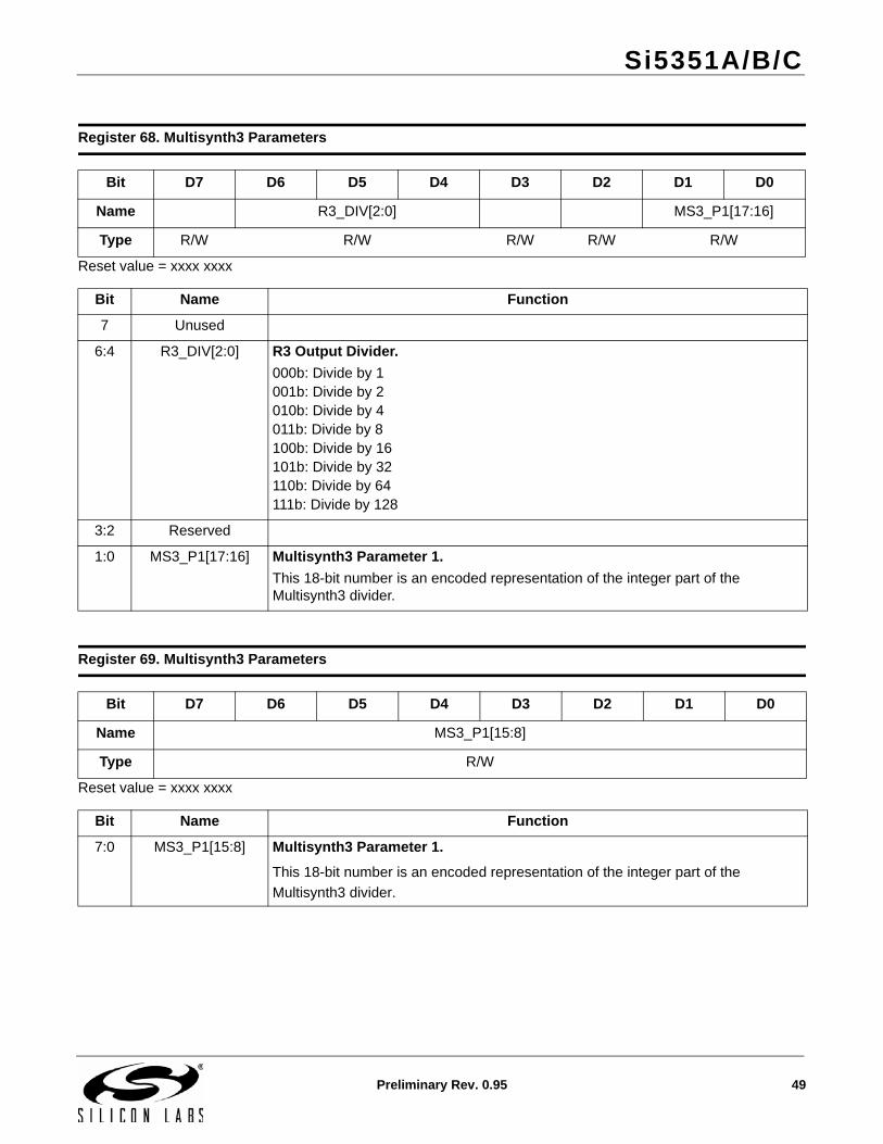
Reset value = xxxx xxxx
Reset value = xxxx xxxx
Register 68. Multisynth3 Parameters
Bit D7 D6 D5 D4 D3 D2 D1 D0
Name R3_DIV[2:0] MS3_P1[17:16]
Type R/W R/W R/W R/W R/W
Bit Name Function
7 Unused
6:4 R3_DIV[2:0] R3 Output Divider.
000b: Divide by 1001b: Divide by 2010b: Divide by 4011b: Divide by 8100b: Divide by 16101b: Divide by 32110b: Divide by 64111b: Divide by 128
3:2 Reserved
1:0 MS3_P1[17:16] Multisynth3 Parameter 1.
This 18-bit number is an encoded representation of the integer part of the Multisynth3 divider.
Register 69. Multisynth3 Parameters
Bit D7 D6 D5 D4 D3 D2 D1 D0
Name MS3_P1[15:8]
Type R/W
Bit Name Function
7:0 MS3_P1[15:8] Multisynth3 Parameter 1.
This 18-bit number is an encoded representation of the integer part of the
Multisynth3 divider.

Si5351A/B/C
50 Preliminary Rev. 0.95
Reset value = xxxx xxxx
Reset value = xxxx xxxx
Reset value = xxxx xxxx
Register 70. Multisynth3 Parameters
Bit D7 D6 D5 D4 D3 D2 D1 D0
Name MS3_P1[7:0]
Type R/W
Bit Name Function
7:0 MS3_P1[7:0] Multisynth3 Parameter 1.
This 18-bit number is an encoded representation of the integer part of the
Multisynth3 divider.
Register 71. Multisynth3 Parameters
Bit D7 D6 D5 D4 D3 D2 D1 D0
Name MS3_P3[19:16] MS3_P2[19:16]
Type R/W R/W
Bit Name Function
7:4 MS3_P3[19:16] Multisynth3 Parameter 3.
This 20-bit number is an encoded representation of the denominator for the frac-tional part of the Multisynth3 divider
3:0 MS3_P2[19:16] Multisynth3 Parameter 2.
This 20-bit number is an encoded representation of the numerator for the fractional part of the MultiSynth3 divider.
Register 72. Multisynth3 Parameters
Bit D7 D6 D5 D4 D3 D2 D1 D0
Name MS3_P2[15:8]
Type R/W
Bit Name Function
7:0 MS3_P2[15:8] Multisynth3 Parameter 2.
This 20-bit number is an encoded representation of the numerator for the fractional part of the Multisynth3 divider.

Si5351A/B/C
Preliminary Rev. 0.95 51
Reset value = xxxx xxxx
Reset value = xxxx xxxx
Reset value = xxxx xxxx
Register 73. Multisynth3 Parameters
Bit D7 D6 D5 D4 D3 D2 D1 D0
Name MS3_P2[7:0]
Type R/W
Bit Name Function
7:0 MS3_P2[7:0] Multisynth3 Parameter 2.
This 20-bit number is an encoded representation of the numerator for the fractional
part of the Multisynth3 divider.
Register 74. Multisynth4 Parameters
Bit D7 D6 D5 D4 D3 D2 D1 D0
Name MS4_P3[15:8]
Type R/W
Bit Name Function
7:0 MS4_P3[15:8] Multisynth4 Parameter 3.
This 20-bit number is an encoded representation of the denominator for the frac-tional part of the Multisynth4 divider.
Register 75. Multisynth4 Parameters
Bit D7 D6 D5 D4 D3 D2 D1 D0
Name MS4_P3[7:0]
Type R/W
Bit Name Function
7:0 MS4_P3[7:0] Multisynth4 Parameter 3.
This 20-bit number is an encoded representation of the numerator for the fractional
part of the Multisynth4 divider.
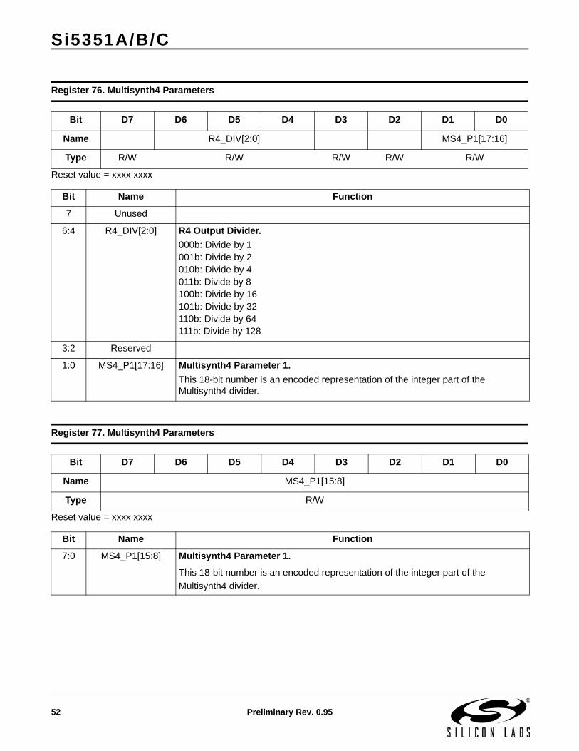
Si5351A/B/C
52 Preliminary Rev. 0.95
Reset value = xxxx xxxx
Reset value = xxxx xxxx
Register 76. Multisynth4 Parameters
Bit D7 D6 D5 D4 D3 D2 D1 D0
Name R4_DIV[2:0] MS4_P1[17:16]
Type R/W R/W R/W R/W R/W
Bit Name Function
7 Unused
6:4 R4_DIV[2:0] R4 Output Divider.
000b: Divide by 1001b: Divide by 2010b: Divide by 4011b: Divide by 8100b: Divide by 16101b: Divide by 32110b: Divide by 64111b: Divide by 128
3:2 Reserved
1:0 MS4_P1[17:16] Multisynth4 Parameter 1.
This 18-bit number is an encoded representation of the integer part of the Multisynth4 divider.
Register 77. Multisynth4 Parameters
Bit D7 D6 D5 D4 D3 D2 D1 D0
Name MS4_P1[15:8]
Type R/W
Bit Name Function
7:0 MS4_P1[15:8] Multisynth4 Parameter 1.
This 18-bit number is an encoded representation of the integer part of the
Multisynth4 divider.

Si5351A/B/C
Preliminary Rev. 0.95 53
Reset value = xxxx xxxx
Reset value = xxxx xxxx
Reset value = xxxx xxxx
Register 78. Multisynth4 Parameters
Bit D7 D6 D5 D4 D3 D2 D1 D0
Name MS4_P1[7:0]
Type R/W
Bit Name Function
7:0 MS4_P1[7:0] Multisynth4 Parameter 1.
This 18-bit number is an encoded representation of the integer part of the
Multisynth4 divider.
Register 79. Multisynth4 Parameters
Bit D7 D6 D5 D4 D3 D2 D1 D0
Name MS4_P3[19:16] MS4_P2[19:16]
Type R/W R/W
Bit Name Function
7:4 MS4_P3[19:16] Multisynth4 Parameter 3.
This 20-bit number is an encoded representation of the denominator for the frac-tional part of the Multisynth4 divider
3:0 MS4_P2[19:16] Multisynth4 Parameter 2.
This 20-bit number is an encoded representation of the numerator for the fractional part of the MultiSynth4 divider.
Register 80. Multisynth4 Parameters
Bit D7 D6 D5 D4 D3 D2 D1 D0
Name MS4_P2[15:8]
Type R/W
Bit Name Function
7:0 MS4_P2[15:8] Multisynth4 Parameter 2.
This 20-bit number is an encoded representation of the numerator for the fractional part of the Multisynth4 Divider.

Si5351A/B/C
54 Preliminary Rev. 0.95
Reset value = xxxx xxxx
Reset value = xxxx xxxx
Reset value = xxxx xxxx
Register 81. Multisynth4 Parameters
Bit D7 D6 D5 D4 D3 D2 D1 D0
Name MS4_P2[7:0]
Type R/W
Bit Name Function
7:0 MS4_P2[7:0] Multisynth4 Parameter 2.
This 20-bit number is an encoded representation of the numerator for the fractional
part of the Multisynth4 divider.
Register 82. Multisynth5 Parameters
Bit D7 D6 D5 D4 D3 D2 D1 D0
Name MS5_P3[15:8]
Type R/W
Bit Name Function
7:0 MS5_P3[15:8] Multisynth5 Parameter 3.
This 20-bit number is an encoded representation of the denominator for the frac-tional part of the Multisynth5 divider.
Register 83. Multisynth5 Parameters
Bit D7 D6 D5 D4 D3 D2 D1 D0
Name MS5_P3[7:0]
Type R/W
Bit Name Function
7:0 MS5_P3[7:0] Multisynth5 Parameter 3.
This 20-bit number is an encoded representation of the denominator for the frac-
tional part of the Multisynth5 divider.

Si5351A/B/C
Preliminary Rev. 0.95 55
Reset value = xxxx xxxx
Reset value = xxxx xxxx
Register 84. Multisynth5 Parameters
Bit D7 D6 D5 D4 D3 D2 D1 D0
Name R5_DIV[2:0] MS5_P1[17:16]
Type R/W R/W R/W R/W R/W
Bit Name Function
7 Unused
6:4 R5_DIV[2:0] R5 Output Divider.
000b: Divide by 1001b: Divide by 2010b: Divide by 4011b: Divide by 8100b: Divide by 16101b: Divide by 32110b: Divide by 64111b: Divide by 128
3:2 Reserved
1:0 MS5_P1[17:16] Multisynth5 Parameter 1.
This 18-bit number is an encoded representation of the integer part of the Multisynth5 divider.
Register 85. Multisynth5 Parameters
Bit D7 D6 D5 D4 D3 D2 D1 D0
Name MS5_P1[15:8]
Type R/W
Bit Name Function
7:0 MS5_P1[15:8] Multisynth5 Parameter 1.
This 18-bit number is an encoded representation of the integer part of the
Multisynth5 divider.

Si5351A/B/C
56 Preliminary Rev. 0.95
Reset value = xxxx xxxx
Reset value = xxxx xxxx
Reset value = xxxx xxxx
Register 86. Multisynth5 Parameters
Bit D7 D6 D5 D4 D3 D2 D1 D0
Name MS5_P1[7:0]
Type R/W
Bit Name Function
7:0 MS5_P1[7:0] Multisynth5 Parameter 1.
This 18-bit number is an encoded representation of the integer part of the
Multisynth5 divider.
Register 87. Multisynth5 Parameters
Bit D7 D6 D5 D4 D3 D2 D1 D0
Name MS5_P3[19:16] MS5_P2[19:16]
Type R/W R/W
Bit Name Function
7:4 MS5_P3[19:16] Multisynth5 Parameter 3.
This 20-bit number is an encoded representation of the denominator for the frac-tional part of the Multisynth5 divider
3:0 MS5_P2[19:16] Multisynth5 Parameter 2.
This 20-bit number is an encoded representation of the numerator for the fractional part of the MultiSynth5 divider.
Register 88. Multisynth5 Parameters
Bit D7 D6 D5 D4 D3 D2 D1 D0
Name MS5_P2[15:8]
Type R/W
Bit Name Function
7:0 MS5_P2[15:8] Multisynth5 Parameter 2.
This 20-bit number is an encoded representation of the numerator for the fractional
part of the Multisynth5 Divider.
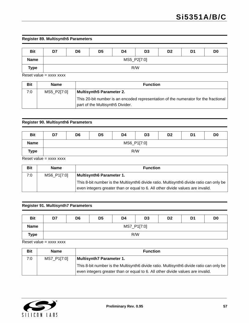
Si5351A/B/C
Preliminary Rev. 0.95 57
Reset value = xxxx xxxx
Reset value = xxxx xxxx
Reset value = xxxx xxxx
Register 89. Multisynth5 Parameters
Bit D7 D6 D5 D4 D3 D2 D1 D0
Name MS5_P2[7:0]
Type R/W
Bit Name Function
7:0 MS5_P2[7:0] Multisynth5 Parameter 2.
This 20-bit number is an encoded representation of the numerator for the fractional
part of the Multisynth5 Divider.
Register 90. Multisynth6 Parameters
Bit D7 D6 D5 D4 D3 D2 D1 D0
Name MS6_P1[7:0]
Type R/W
Bit Name Function
7:0 MS6_P1[7:0] Multisynth6 Parameter 1.
This 8-bit number is the Multisynth6 divide ratio. Multisynth6 divide ratio can only be
even integers greater than or equal to 6. All other divide values are invalid.
Register 91. Multisynth7 Parameters
Bit D7 D6 D5 D4 D3 D2 D1 D0
Name MS7_P1[7:0]
Type R/W
Bit Name Function
7:0 MS7_P1[7:0] Multisynth7 Parameter 1.
This 8-bit number is the Multisynth6 divide ratio. Multisynth6 divide ratio can only be
even integers greater than or equal to 6. All other divide values are invalid.

Si5351A/B/C
58 Preliminary Rev. 0.95
Reset value = xxxx xxxx
Register 92. Clock 6 and 7 Output Divider
Bit D7 D6 D5 D4 D3 D2 D1 D0
Name R7_DIV[2:0] R6_DIV[2:0]
Type R/W R/W R/W R/W
Bit Name Function
7 Reserved Leave as default.
6:4 R7_DIV[2:0] R7 Output Divider.
000b: Divide by 1001b: Divide by 2010b: Divide by 4011b: Divide by 8100b: Divide by 16101b: Divide by 32110b: Divide by 64111b: Divide by 128
3 Reserved Leave as default.
1:0 R6_DIV[2:0] R6 Output Divider.
000b: Divide by 1001b: Divide by 2010b: Divide by 4011b: Divide by 8100b: Divide by 16101b: Divide by 32110b: Divide by 64111b: Divide by 128
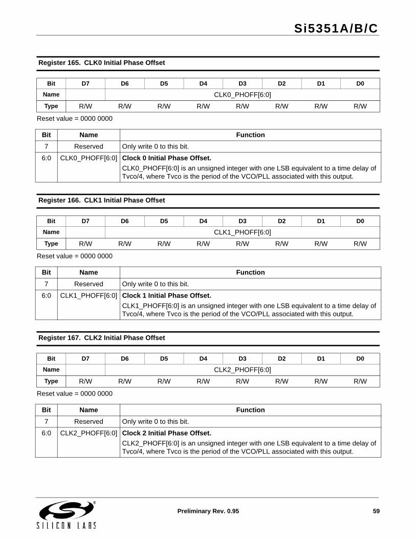
Si5351A/B/C
Preliminary Rev. 0.95 59
Reset value = 0000 0000
Reset value = 0000 0000
Reset value = 0000 0000
Register 165. CLK0 Initial Phase Offset
Bit D7 D6 D5 D4 D3 D2 D1 D0
Name CLK0_PHOFF[6:0]
Type R/W R/W R/W R/W R/W R/W R/W R/W
Bit Name Function
7 Reserved Only write 0 to this bit.
6:0 CLK0_PHOFF[6:0] Clock 0 Initial Phase Offset.
CLK0_PHOFF[6:0] is an unsigned integer with one LSB equivalent to a time delay of Tvco/4, where Tvco is the period of the VCO/PLL associated with this output.
Register 166. CLK1 Initial Phase Offset
Bit D7 D6 D5 D4 D3 D2 D1 D0
Name CLK1_PHOFF[6:0]
Type R/W R/W R/W R/W R/W R/W R/W R/W
Bit Name Function
7 Reserved Only write 0 to this bit.
6:0 CLK1_PHOFF[6:0] Clock 1 Initial Phase Offset.
CLK1_PHOFF[6:0] is an unsigned integer with one LSB equivalent to a time delay of Tvco/4, where Tvco is the period of the VCO/PLL associated with this output.
Register 167. CLK2 Initial Phase Offset
Bit D7 D6 D5 D4 D3 D2 D1 D0
Name CLK2_PHOFF[6:0]
Type R/W R/W R/W R/W R/W R/W R/W R/W
Bit Name Function
7 Reserved Only write 0 to this bit.
6:0 CLK2_PHOFF[6:0] Clock 2 Initial Phase Offset.
CLK2_PHOFF[6:0] is an unsigned integer with one LSB equivalent to a time delay of Tvco/4, where Tvco is the period of the VCO/PLL associated with this output.

Si5351A/B/C
60 Preliminary Rev. 0.95
Reset value = 0000 0000
Reset value = 0000 0000
Reset value = 0000 0000
Register 168. CLK3 Initial Phase Offset
Bit D7 D6 D5 D4 D3 D2 D1 D0
Name CLK3_PHOFF[6:0]
Type R/W R/W R/W R/W R/W R/W R/W R/W
Bit Name Function
7 Reserved Only write 0 to this bit.
6:0 CLK3_PHOFF[6:0] Clock 3 Initial Phase Offset.
CLK3_PHOFF[6:0] is an unsigned integer with one LSB equivalent to a time delay of Tvco/4, where Tvco is the period of the VCO/PLL associated with this output.
Register 169. CLK4 Initial Phase Offset
Bit D7 D6 D5 D4 D3 D2 D1 D0
Name CLK4_PHOFF[6:0]
Type R/W R/W R/W R/W R/W R/W R/W R/W
Bit Name Function
7 Reserved Only write 0 to this bit.
6:0 CLK4_PHOFF[6:0] Clock 4 Initial Phase Offset.
CLK4_PHOFF[6:0] is an unsigned integer with one LSB equivalent to a time delay of Tvco/4, where Tvco is the period of the VCO/PLL associated with this output.
Register 170. CLK5 Initial Phase Offset
Bit D7 D6 D5 D4 D3 D2 D1 D0
Name CLK5_PHOFF[6:0]
Type R/W R/W R/W R/W R/W R/W R/W R/W
Bit Name Function
7 Reserved Only write 0 to this bit.
6:0 CLK5_PHOFF[6:0] Clock 5 Initial Phase Offset.
CLK5_PHOFF[6:0] is an unsigned integer with one LSB equivalent to a time delay of Tvco/4, where Tvco is the period of the VCO/PLL associated with this output.

Si5351A/B/C
Preliminary Rev. 0.95 61
Reset value = 0000 0000
Reset value = 11xx xxxx
Register 177. PLL Reset
Bit D7 D6 D5 D4 D3 D2 D1 D0
Name PLLB_RST PLLA_RST
Type R/W R/W R/W R/W R/W R/W R/W R/W
Bit Name Function
7 PLLB_RST PLLB_Reset.
Writing a 1 to this bit will reset PLLB. This is a self clearing bit (Si5351A/C only).
6 Reserved Leave as default.
5 PLLA_RST PLLA_Reset.
Writing a 1 to this bit will reset PLLA. This is a self clearing bit.
4:0 Reserved Leave as default.
Register 183. Crystal Internal Load Capacitance
Bit D7 D6 D5 D4 D3 D2 D1 D0
Name XTAL_CL[1:0]
Type R/W R/W R/W R/W R/W R/W R/W R/W
Bit Name Function
7:6 XTAL_CL[1:0] Crystal Load Capacitance Selection.
These 2 bits determine the internal load capacitance value for the crystal. See "3.1.1. Crystal Inputs (XA, XB)" on page 11.00: Reserved. Do not select this option.01: Internal CL = 6 pF. 10: Internal CL = 8 pF. 11: Internal CL = 10 pF (default).
5:0 Reserved Leave as default.

Si5351A/B/C
62 Preliminary Rev. 0.95
9. Si5351A Pin Descriptions (20-Pin QFN, 24-Pin QSOP)
Table 10. Si5351A Pin Descriptions
Pin NamePin Number
Pin Type* Function20-QFN 24-QSOP
XA 1 6 I Input pin for external crystal.
XB 2 7 I Input pin for external crystal.
CLK0 13 21 O Output clock 0.
CLK1 12 20 O Output clock 1.
CLK2 9 15 O Output clock 2.
CLK3 8 14 O Output clock 3.
CLK4 19 3 O Output clock 4.
CLK5 17 1 O Output clock 5.
CLK6 16 24 O Output clock 6.
CLK7 15 23 O Output clock 7.
A0 3 9 I I2C address bit.
SCL 4 10 I I2C bus serial clock input. Pull-up to VDD core with 1 k
SDA 5 11 I/O I2C bus serial data input. Pull-up to VDD core with 1 k
SSEN 6 12 I Spread spectrum enable. High = enabled, Low = disabled.
OEB 7 13 I Output driver enable. Low = enabled, High = disabled.
VDD 20 4 P Core voltage supply pin. See 6.2.
VDDOA 11 18 P Output voltage supply pin for CLK0 and CLK1. See 6.2.
VDDOB 10 16 P Output voltage supply pin for CLK2 and CLK3. See 6.2.
VDDOC 18 2 P Output voltage supply pin for CLK4 and CLK5. See 6.2.
VDDOD 14 22 P Output voltage supply pin for CLK6 and CLK7. See 6.2.
GND Center Pad 5, 8, 17, 19 P Ground. Use multiple vias to ensure a solid path to GND.
1. I = Input, O = Output, P = Power. 2. Input pins are not internally pulled up.
1
2
3
4
5
6 7 8 9 10
15
14
13
12
11
20
19 18
17 16
XA
XB
A0
SCL
SDA
OE
B
CL
K3
CL
K2
VD
DO
B
SS
EN
Si5351A 20-QFNTop View
GND PAD
CL
K6
CLK
5
VD
DO
C
CLK
4
VD
D
VDDOA
CLK1
CLK0
VDDOD
CLK7
2
1
4
3
6
5
8
7
10
9
12
11
23
24
21
22
19
20
17
18
15
16
13
14
Si5351A 24-QSOPTop View
CLK7
CLK6
CLK0
VDD0D
GND
CLK1
GND
VDDOA
CLK2
VDD0B
OEB
CLK3
VDDOC
CLK5
VDD
CLK4
XA
GND
GND
XB
SCL
A0
SSEN
SDA

Si5351A/B/C
Preliminary Rev. 0.95 63
10. Si5351B Pin Descriptions (20-Pin QFN, 24-Pin QSOP)
Table 11. Si5351B Pin Descriptions
Pin NamePin Number
Pin Type* Function20-QFN 24-QSOP
XA 1 6 I Input pin for external crystal
XB 2 7 I Input pin for external crystal
CLK0 13 21 O Output clock 0
CLK1 12 20 O Output clock 1
CLK2 9 15 O Output clock 2
CLK3 8 14 O Output clock 3
CLK4 19 3 O Output clock 4
CLK5 17 1 O Output clock 5
CLK6 16 24 O Output clock 6
CLK7 15 23 O Output clock 7
VC 3 9 I VCXO control voltage input
SCL 4 10 I I2C bus serial clock input. Pull-up to VDD core with 1 k
SDA 5 11 I/O I2C bus serial data input. Pull-up to VDD core with 1 k
SSEN 6 12 I Spread spectrum enable. High = enabled, Low = disabled.
OEB 7 13 I Output driver enable. Low = enabled, High = disabled.
VDD 20 4 P Core voltage supply pin
VDDOA 11 18 P Output voltage supply pin for CLK0 and CLK1. See 6.2
VDDOB 10 16 P Output voltage supply pin for CLK2 and CLK3. See 6.2
VDDOC 18 2 P Output voltage supply pin for CLK4 and CLK5. See 6.2
VDDOD 14 22 P Output voltage supply pin for CLK6 and CLK7. See 6.2
GND Center Pad 5, 8, 17, 19 P Ground
*Note: I = Input, O = Output, P = Power*Note: Input pins are not internally pulled up.
1
2
3
4
5
6 7 8 9 10
15
14
13
12
11
20
19 18
17 16
XA
XB
VC
SCL
SDA
OE
B
CLK
3
CLK
2
VD
DO
B
SS
EN
Si5351B 20-QFNTop View
GND PAD
CL
K6
CLK
5
VD
DO
C
CLK
4
VD
D
VDDOA
CLK1
CLK0
VDDOD
CLK7
2
1
4
3
6
5
8
7
10
9
12
11
23
24
21
22
19
20
17
18
15
16
13
14
Si5351B 24-QSOPTop View
VDDOC
CLK5
VDD
CLK4
XA
GND
GND
XB
SCL
VC
SSEN
SDA
CLK7
CLK6
CLK0
VDD0D
GND
CLK1
GND
VDDOA
CLK2
VDD0B
OEB
CLK3

Si5351A/B/C
64 Preliminary Rev. 0.95
11. Si5351C Pin Descriptions (20-Pin QFN, 24-Pin QSOP)
Table 12. Si5351C Pin Descriptions
Pin NamePin Number
Pin Type* Function20-QFN 24-QSOP
XA 1 6 I Input pin for external crystal.
XB 2 7 I Input pin for external crystal.
CLK0 13 21 O Output clock 0.
CLK1 12 20 O Output clock 1.
CLK2 9 15 O Output clock 2.
CLK3 8 14 O Output clock 3.
CLK4 19 3 O Output clock 4.
CLK5 17 1 O Output clock 5.
CLK6 16 24 O Output clock 6.
CLK7 15 23 O Output clock 7.
INTR 3 9 O Interrupt pin. Open drain active low output, requires a pull-up resistor greater than 1 k
SCL 4 10 I I2C bus serial clock input. Pull-up to VDD core with 1 k
SDA 5 11 I/O I2C bus serial data input. Pull-up to VDD core with 1 k
CLKIN 6 12 I PLL clock input.
OEB 7 13 I Output driver enable. Low = enabled, High = disabled.
VDD 20 4 P Core voltage supply pin
VDDOA 11 18 P Output voltage supply pin for CLK0 and CLK1. See 6.2
VDDOB 10 16 P Output voltage supply pin for CLK2 and CLK3. See 6.2
VDDOC 18 2 P Output voltage supply pin for CLK4 and CLK5. See 6.2
VDDOD 14 22 P Output voltage supply pin for CLK6 and CLK7. See 6.2
GND Center Pad 5, 8, 17, 19 P Ground.
Notes:1. I = Input, O = Output, P = Power.2. Input pins are not internally pulled up.
1
2
3
4
5
6 7 8 9 10
15
14
13
12
11
20
19 18 17 16
XA
XB
INTR
SCL
SDA
OE
B
CLK
3
CLK
2
VD
DO
B
CL
KIN
Si5351C 20-QFNTop View
GND PAD
CL
K6
CLK
5
VD
DO
C
CLK
4
VD
D
VDDOA
CLK1
CLK0
VDDOD
CLK7
2
1
4
3
6
5
8
7
10
9
12
11
23
24
21
22
19
20
17
18
15
16
13
14
Si5351C 24-QSOPTop View
VDDOC
CLK5
VDD
CLK4
XA
GND
GND
XB
SCL
INTR
CLKIN
SDA
CLK7
CLK6
CLK0
VDD0D
GND
CLK1
GND
VDDOA
CLK2
VDD0B
OEB
CLK3

Si5351A/B/C
Preliminary Rev. 0.95 65
12. Si5351A Pin Descriptions (10-Pin MSOP)
Table 13. Si5351A 10-MSOP Pin Descriptions
Pin Name
Pin Number Pin Type* Function
10-MSOP
XA 2 I Input pin for external crystal.
XB 3 I Input pin for external crystal.
CLK0 10 O Output clock 0.
CLK1 9 O Output clock 1.
CLK2 6 O Output clock 2.
SCL 4 I Serial clock input for the I2C bus. This pin must be pulled-up using a pull-
up resistor of at least 1 k.
SDA 5 I/O Serial data input for the I2C bus. This pin must be pulled-up using a pull-up resistor of at least 1 k.
VDD 1 P Core voltage supply pin.
VDDO 7 P Output voltage supply pin for CLK0, CLK1, and CLK2. See "6.2. Power Supply Sequencing" on page 21.
GND 8 P Ground.
*Note: I = Input, O = Output, P = Power
Si5351A 10-MSOPTop View
XA
VDD
SCL
XB
2
1
4
3
CLK1
CLK0
VDDO
GND
9
10
7
8
SDA 5 CLK26
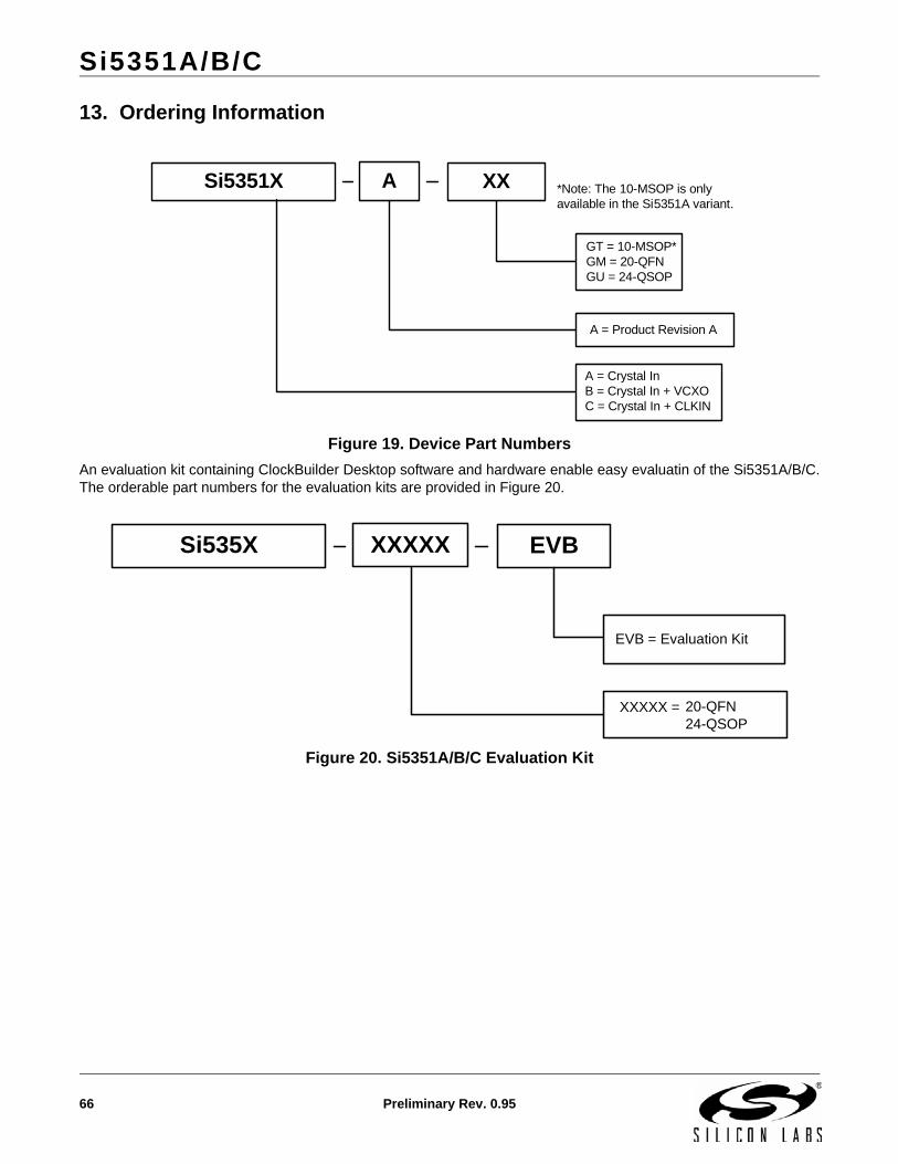
Si5351A/B/C
66 Preliminary Rev. 0.95
13. Ordering Information
Figure 19. Device Part Numbers
An evaluation kit containing ClockBuilder Desktop software and hardware enable easy evaluatin of the Si5351A/B/C.The orderable part numbers for the evaluation kits are provided in Figure 20.
Figure 20. Si5351A/B/C Evaluation Kit
Si5351X XXA
A = Product Revision A
A = Crystal InB = Crystal In + VCXOC = Crystal In + CLKIN
GT = 10-MSOP*GM = 20-QFNGU = 24-QSOP
*Note: The 10-MSOP is only available in the Si5351A variant.
Si535X EVBXXXXX
XXXXX =
EVB = Evaluation Kit
20-QFN24-QSOP

Si5351A/B/C
Preliminary Rev. 0.95 67
14. Package Outline (24-Pin QSOP)
Table 14. 24-QSOP Package Dimensions
Dimension Min Nom Max
A — — 1.75
A1 0.10 — 0.25
b 0.19 — 0.30
c 0.15 — 0.25
D 8.55 8.65 8.75
E 6.00 BSC
E1 3.81 3.90 3.99
e 0.635 BSC
L 0.40 — 1.27
L2 0.25 BSC
q 0 — 8
aaa 0.10
bbb 0.17
ccc 0.10
Notes:1. All dimensions shown are in millimeters (mm) unless otherwise noted.2. Dimensioning and Tolerancing per ANSI Y14.5M-1994.3. This drawing conforms to the JEDEC Solid State Outline MO-137, Variation C 4. Recommended card reflow profile is per the JEDEC/IPC J-STD-020 specification for Small Body
Components.
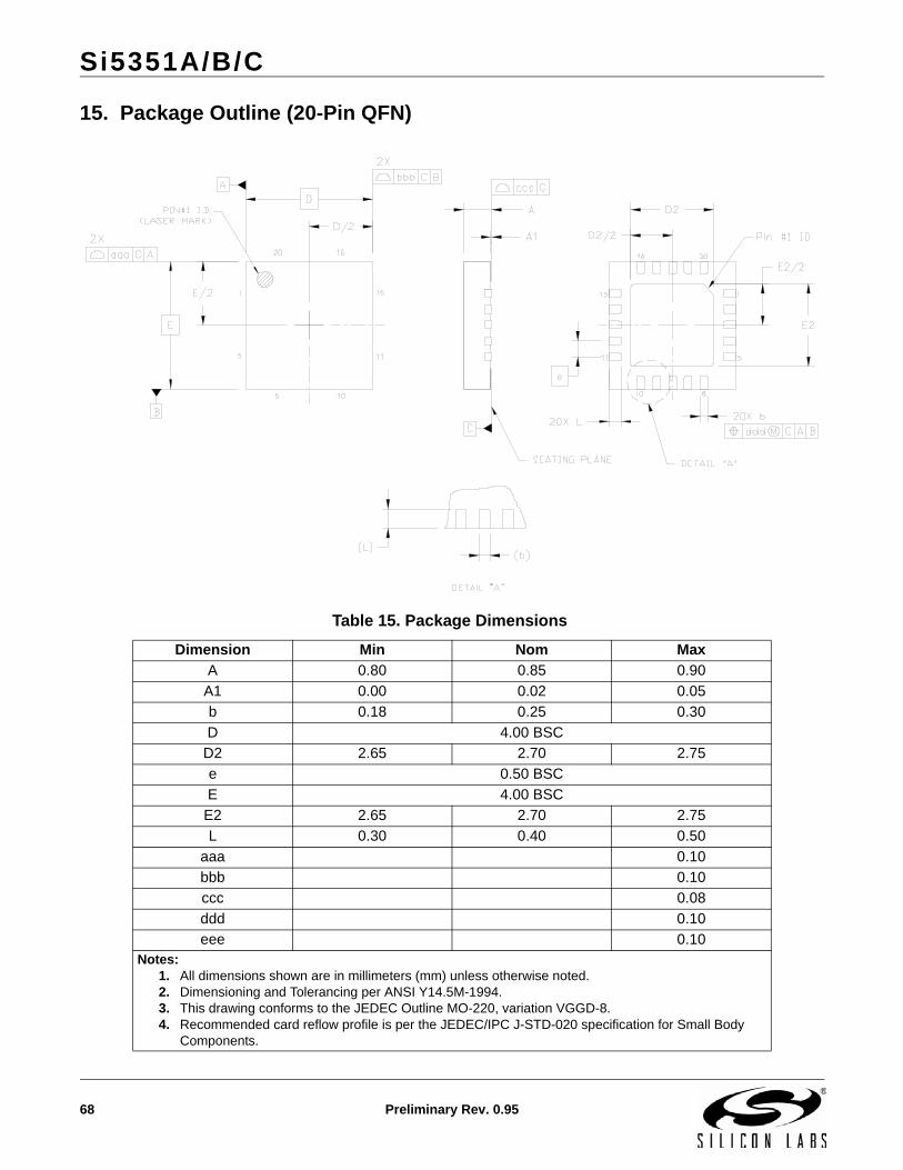
Si5351A/B/C
68 Preliminary Rev. 0.95
15. Package Outline (20-Pin QFN)
Table 15. Package Dimensions
Dimension Min Nom Max
A 0.80 0.85 0.90
A1 0.00 0.02 0.05
b 0.18 0.25 0.30
D 4.00 BSC
D2 2.65 2.70 2.75
e 0.50 BSC
E 4.00 BSC
E2 2.65 2.70 2.75
L 0.30 0.40 0.50
aaa 0.10
bbb 0.10
ccc 0.08
ddd 0.10
eee 0.10Notes:
1. All dimensions shown are in millimeters (mm) unless otherwise noted.2. Dimensioning and Tolerancing per ANSI Y14.5M-1994.3. This drawing conforms to the JEDEC Outline MO-220, variation VGGD-8. 4. Recommended card reflow profile is per the JEDEC/IPC J-STD-020 specification for Small Body
Components.
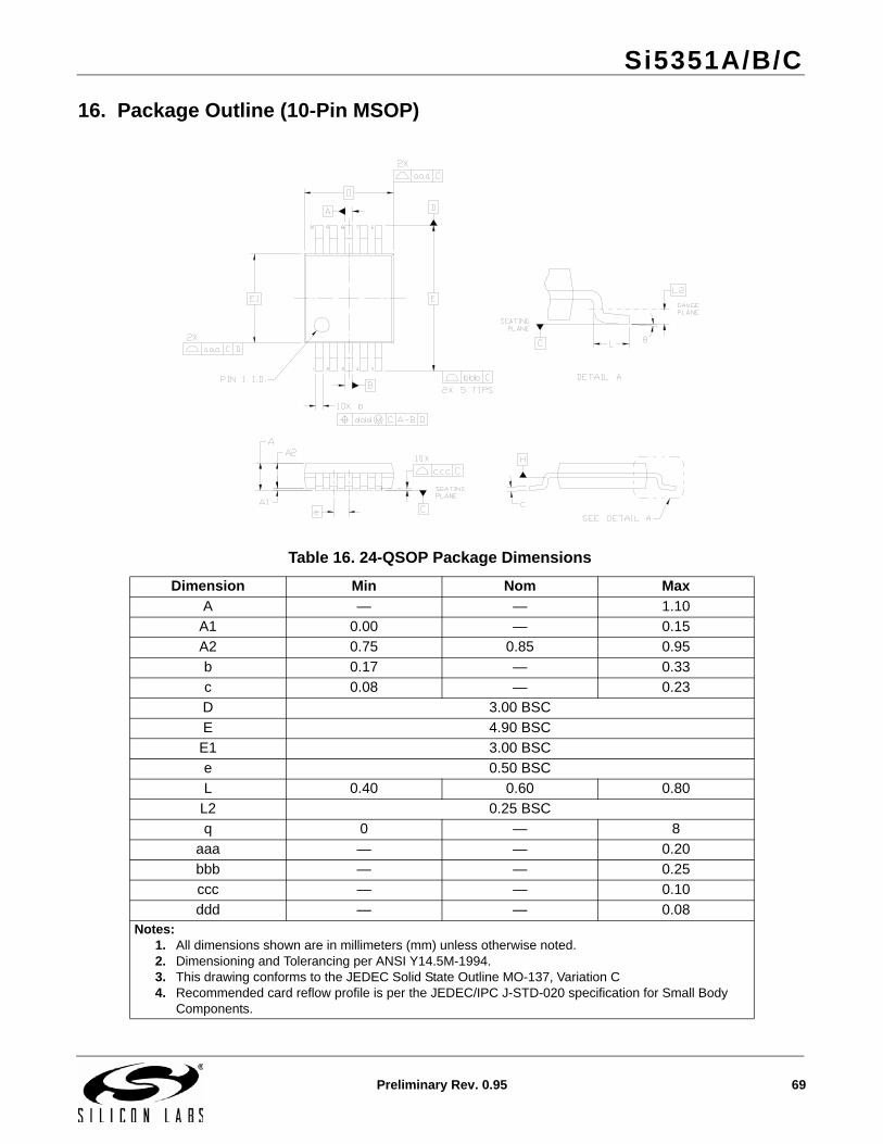
Si5351A/B/C
Preliminary Rev. 0.95 69
16. Package Outline (10-Pin MSOP)
Table 16. 24-QSOP Package Dimensions
Dimension Min Nom Max
A — — 1.10
A1 0.00 — 0.15
A2 0.75 0.85 0.95
b 0.17 — 0.33
c 0.08 — 0.23
D 3.00 BSC
E 4.90 BSC
E1 3.00 BSC
e 0.50 BSC
L 0.40 0.60 0.80
L2 0.25 BSC
q 0 — 8
aaa — — 0.20
bbb — — 0.25
ccc — — 0.10
ddd — — 0.08Notes:
1. All dimensions shown are in millimeters (mm) unless otherwise noted.2. Dimensioning and Tolerancing per ANSI Y14.5M-1994.3. This drawing conforms to the JEDEC Solid State Outline MO-137, Variation C 4. Recommended card reflow profile is per the JEDEC/IPC J-STD-020 specification for Small Body
Components.
Si5351A/B/C
70 Preliminary Rev. 0.95
DOCUMENT CHANGE LIST
Revision 0.1 to Revision 0.9 Updated max output frequency.
Updated kV values in Table 3 on page 5.
Updated "3.4. Spread Spectrum" on page 13.
Added "5.1. Writing a Custom Configuration to RAM" on page 16.
Added "5.7. HCSL Compatible Outputs" on page 20.
Added "6.6. Trace Characteristics" on page 22.
Updated "8. Register Descriptions" on page 25.Added register descriptions.
Revision 0.9 to Revision 0.95 Added 1.8 V VDDO support.
Updated Table 2, “DC Characteristics,” on page 4.
Added soldering profile specs to Table 9, “Absolute
Maximum Ratings1,” on page 8.
Si5351A/B/C
Preliminary Rev. 0.95 71
NOTES:

Si5351A/B/C
72 Preliminary Rev. 0.95
CONTACT INFORMATIONSilicon Laboratories Inc.
400 West Cesar ChavezAustin, TX 78701Tel: 1+(512) 416-8500Fax: 1+(512) 416-9669Toll Free: 1+(877) 444-3032
Please visit the Silicon Labs Technical Support web page:https://www.silabs.com/support/pages/contacttechnicalsupport.aspxand register to submit a technical support request.
Silicon Laboratories and Silicon Labs are trademarks of Silicon Laboratories Inc.Other products or brandnames mentioned herein are trademarks or registered trademarks of their respective holders.
The information in this document is believed to be accurate in all respects at the time of publication but is subject to change without notice. Silicon Laboratories assumes no responsibility for errors and omissions, and disclaims responsibility for any consequences resulting from the use of information included herein. Additionally, Silicon Laboratories assumes no responsibility for the functioning of undescribed features or parameters. Silicon Laboratories reserves the right to make changes without further notice. Silicon Laboratories makes no warranty, rep-resentation or guarantee regarding the suitability of its products for any particular purpose, nor does Silicon Laboratories assume any liability arising out of the application or use of any product or circuit, and specifically disclaims any and all liability, including without limitation conse-quential or incidental damages. Silicon Laboratories products are not designed, intended, or authorized for use in applications intended to support or sustain life, or for any other application in which the failure of the Silicon Laboratories product could create a situation where per-sonal injury or death may occur. Should Buyer purchase or use Silicon Laboratories products for any such unintended or unauthorized ap-plication, Buyer shall indemnify and hold Silicon Laboratories harmless against all claims and damages.