Si47xx-EVB -- Si47xx-EVB User's Guide
164
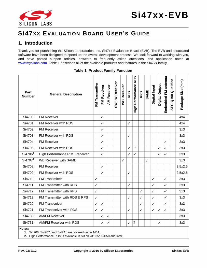
Rev. 0.8 2/12 Copyright © 2016 by Silicon Laboratories Si47xx-EVB Si47xx-EVB Si47 XX E VALUATION B OARD U SER ’ S G UIDE 1. Introduction Thank you for purchasing the Silicon Laboratories, Inc. Si47xx Evaluation Board (EVB). The EVB and associated software have been designed to speed up the overall development process. We look forward to working with you, and have posted support articles, answers to frequently asked questions, and application notes at www.mysilabs.com. Table 1 describes all of the available products and features in the Si47xx family. Table 1. Product Family Function Part Number General Description FM Transmitter FM Receiver AM Receiver SW/LW Receiver WB Receiver RDS High Performance RDS RPS SAME Digital Input Digital Output Embedded FM antenna AEC-Q100 Qualified Package Size (mm) Si4700 FM Receiver 4x4 Si4701 FM Receiver with RDS 4x4 Si4702 FM Receiver 3x3 Si4703 FM Receiver with RDS 3x3 Si4704 FM Receiver 3x3 Si4705 FM Receiver with RDS 2 3x3 Si4706 1 High Performance RDS Receiver 3x3 Si4707 1 WB Receiver with SAME 3x3 Si4708 FM Receiver 2.5x2.5 Si4709 FM Receiver with RDS 2.5x2.5 Si4710 FM Transmitter 3x3 Si4711 FM Transmitter with RDS 3x3 Si4712 FM Transmitter with RPS 3x3 Si4713 FM Transmitter with RDS & RPS 3x3 Si4720 FM Transceiver 3x3 Si4721 FM Transceiver with RDS 3x3 Si4730 AM/FM Receiver 3x3 Si4731 AM/FM Receiver with RDS 2 3x3 Notes: 1. Si4706, Si4707, and Si474x are covered under NDA. 2. High Performance RDS is available in Si4705/31/35/85-D50 and later.
Transcript of Si47xx-EVB -- Si47xx-EVB User's Guide
Rev. 0.8 2/12 Copyright © 2016 by Silicon Laboratories Si47xx-EVB
Si47xx-EVB
Si47XX EVALUATION BOARD USER’S GUIDE
1. Introduction
Thank you for purchasing the Silicon Laboratories, Inc. Si47xx Evaluation Board (EVB). The EVB and associatedsoftware have been designed to speed up the overall development process. We look forward to working with you,and have posted support articles, answers to frequently asked questions, and application notes atwww.mysilabs.com. Table 1 describes all of the available products and features in the Si47xx family.
Table 1. Product Family Function
Part Number
General DescriptionF
M T
ran
smit
ter
FM
Re
ceiv
er
AM
Re
ce
ive
r
SW
/LW
Re
ceiv
er
WB
Re
cei
ver
RD
S
Hig
h P
erf
orm
an
ce
RD
S
RP
S
SA
ME
Dig
ita
l In
pu
t
Dig
ital
Ou
tpu
t
Em
bed
de
d F
M a
nte
nn
a
AE
C-Q
100
Qu
alif
ied
Pa
cka
ge
Siz
e (
mm
)
Si4700 FM Receiver 4x4
Si4701 FM Receiver with RDS 4x4
Si4702 FM Receiver 3x3
Si4703 FM Receiver with RDS 3x3
Si4704 FM Receiver 3x3
Si4705 FM Receiver with RDS 2
3x3
Si47061 High Performance RDS Receiver 3x3
Si47071 WB Receiver with SAME 3x3
Si4708 FM Receiver 2.5x2.5
Si4709 FM Receiver with RDS 2.5x2.5
Si4710 FM Transmitter 3x3
Si4711 FM Transmitter with RDS 3x3
Si4712 FM Transmitter with RPS 3x3
Si4713 FM Transmitter with RDS & RPS 3x3
Si4720 FM Transceiver 3x3
Si4721 FM Transceiver with RDS 3x3
Si4730 AM/FM Receiver 3x3
Si4731 AM/FM Receiver with RDS 2 3x3
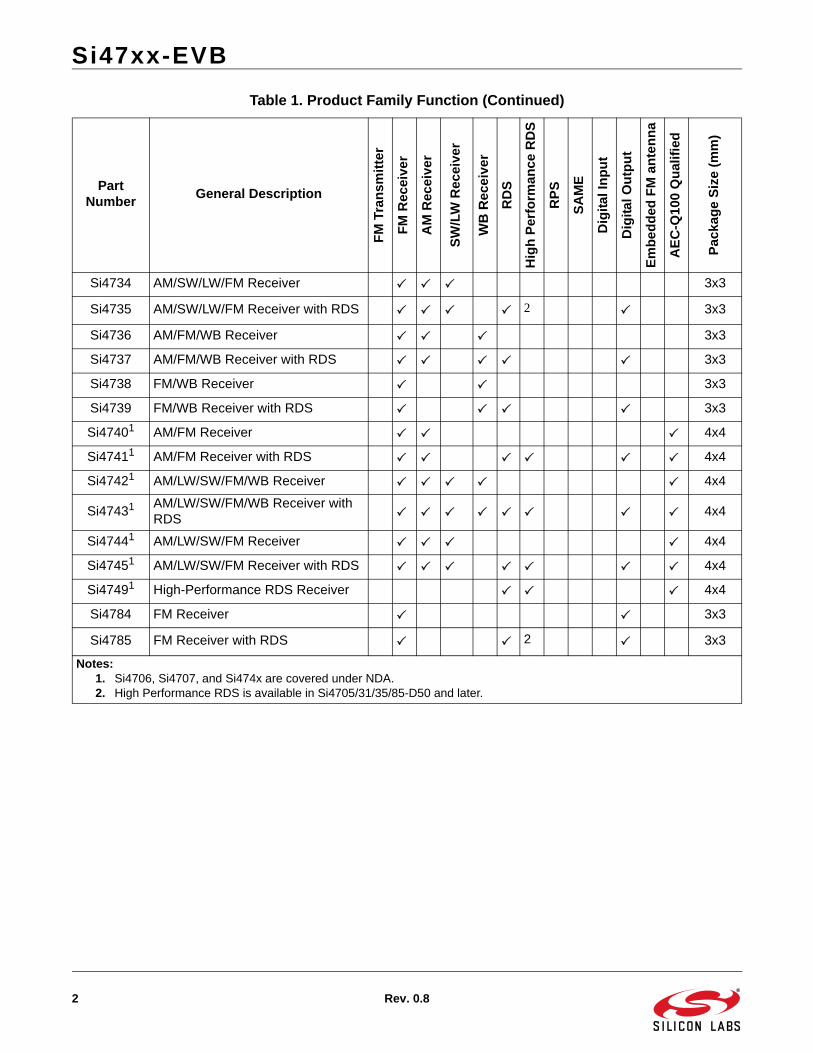
Notes:1. Si4706, Si4707, and Si474x are covered under NDA.2. High Performance RDS is available in Si4705/31/35/85-D50 and later.
Si47xx-EVB
2 Rev. 0.8
Si4734 AM/SW/LW/FM Receiver 3x3
Si4735 AM/SW/LW/FM Receiver with RDS 2 3x3
Si4736 AM/FM/WB Receiver 3x3
Si4737 AM/FM/WB Receiver with RDS 3x3
Si4738 FM/WB Receiver 3x3
Si4739 FM/WB Receiver with RDS 3x3
Si47401 AM/FM Receiver 4x4
Si47411 AM/FM Receiver with RDS 4x4
Si47421 AM/LW/SW/FM/WB Receiver 4x4
Si47431 AM/LW/SW/FM/WB Receiver with RDS 4x4
Si47441 AM/LW/SW/FM Receiver 4x4
Si47451 AM/LW/SW/FM Receiver with RDS 4x4
Si47491 High-Performance RDS Receiver 4x4
Si4784 FM Receiver 3x3
Si4785 FM Receiver with RDS 2 3x3
Table 1. Product Family Function (Continued)
Part Number
General Description
FM
Tra
nsm
itte
r
FM
Rec
eive
r
AM
Rec
eiv
er
SW
/LW
Rec
eive
r
WB
Re
ceiv
er
RD
S
Hig
h P
erf
orm
an
ce
RD
S
RP
S
SA
ME
Dig
ital
In
pu
t
Dig
ita
l O
utp
ut
Em
be
dd
ed F
M a
nte
nn
a
AE
C-Q
100
Qu
alif
ied
Pac
kag
e S
ize
(mm
)
Notes:1. Si4706, Si4707, and Si474x are covered under NDA.2. High Performance RDS is available in Si4705/31/35/85-D50 and later.
Si47xx-EVB
Rev. 0.8 3
TABLE OF CONTENTS
1. Introduction . . . . . . . . . . . . . . . . . . . . . . . . . . . . . . . . . . . . . . . . . . . . . . . . . . . . . . . . . . . . .12. Description . . . . . . . . . . . . . . . . . . . . . . . . . . . . . . . . . . . . . . . . . . . . . . . . . . . . . . . . . . . . . .8
2.1. Si47xx Baseboard . . . . . . . . . . . . . . . . . . . . . . . . . . . . . . . . . . . . . . . . . . . . . . . . . . . .82.2. Si47xx Daughtercards . . . . . . . . . . . . . . . . . . . . . . . . . . . . . . . . . . . . . . . . . . . . . . . .15
3. Recommended Hardware Setup . . . . . . . . . . . . . . . . . . . . . . . . . . . . . . . . . . . . . . . . . . . .283.1. Hardware Setup for FM Transmitter Test . . . . . . . . . . . . . . . . . . . . . . . . . . . . . . . . .283.2. Hardware Setup for FM or Weather Band Receiver Test . . . . . . . . . . . . . . . . . . . . .293.3. Hardware Setup for AM Receiver Test . . . . . . . . . . . . . . . . . . . . . . . . . . . . . . . . . . .30
4. Getting Started . . . . . . . . . . . . . . . . . . . . . . . . . . . . . . . . . . . . . . . . . . . . . . . . . . . . . . . . . .324.1. Software Installation . . . . . . . . . . . . . . . . . . . . . . . . . . . . . . . . . . . . . . . . . . . . . . . . .324.2. Board Initialization . . . . . . . . . . . . . . . . . . . . . . . . . . . . . . . . . . . . . . . . . . . . . . . . . . .334.3. Switching Functions . . . . . . . . . . . . . . . . . . . . . . . . . . . . . . . . . . . . . . . . . . . . . . . . .364.4. State Management . . . . . . . . . . . . . . . . . . . . . . . . . . . . . . . . . . . . . . . . . . . . . . . . . .374.5. Disconnecting the EVB . . . . . . . . . . . . . . . . . . . . . . . . . . . . . . . . . . . . . . . . . . . . . . .39
5. FM Transmitter GUI . . . . . . . . . . . . . . . . . . . . . . . . . . . . . . . . . . . . . . . . . . . . . . . . . . . . . .405.1. Configuring the Si47xx as an FM Transmitter Using Analog Audio Input . . . . . . . . .405.2. Configuring the Si47xx as an FM Transmitter Using Digital Audio with
Analog Audio Source . . . . . . . . . . . . . . . . . . . . . . . . . . . . . . . . . . . . . . . . . . . . . . . . .415.3. Configuring the Si47xx as an FM Transmitter Using Digital Audio with
SPDIF Digital Source . . . . . . . . . . . . . . . . . . . . . . . . . . . . . . . . . . . . . . . . . . . . . . . .425.4. FM Transmitter Main Window . . . . . . . . . . . . . . . . . . . . . . . . . . . . . . . . . . . . . . . . . .435.5. FM Transmitter Settings (Analog Mode) Property Window . . . . . . . . . . . . . . . . . . . .455.6. FM Transmitter Settings (Digital Mode) Property Window . . . . . . . . . . . . . . . . . . . .475.7. CODEC Settings . . . . . . . . . . . . . . . . . . . . . . . . . . . . . . . . . . . . . . . . . . . . . . . . . . . .495.8. SPDIF Settings . . . . . . . . . . . . . . . . . . . . . . . . . . . . . . . . . . . . . . . . . . . . . . . . . . . . .505.9. FM Transmitter Receive Power Scan Window . . . . . . . . . . . . . . . . . . . . . . . . . . . . .515.10. FM Transmitter Radio Data Service (RDS) . . . . . . . . . . . . . . . . . . . . . . . . . . . . . . .525.11. FM Transmitter Register Map Window . . . . . . . . . . . . . . . . . . . . . . . . . . . . . . . . . .60
6. FM Receiver GUI . . . . . . . . . . . . . . . . . . . . . . . . . . . . . . . . . . . . . . . . . . . . . . . . . . . . . . . . .616.1. Configuring the Si47xx as an FM Receiver . . . . . . . . . . . . . . . . . . . . . . . . . . . . . . . .616.2. FM Receiver Main Window . . . . . . . . . . . . . . . . . . . . . . . . . . . . . . . . . . . . . . . . . . . .626.3. FM Receiver Settings Property Window . . . . . . . . . . . . . . . . . . . . . . . . . . . . . . . . . .646.4. CODEC and SPDIF Settings . . . . . . . . . . . . . . . . . . . . . . . . . . . . . . . . . . . . . . . . . . .736.5. FM Receiver RDS Window . . . . . . . . . . . . . . . . . . . . . . . . . . . . . . . . . . . . . . . . . . . .746.6. FM Receiver RDS Settings . . . . . . . . . . . . . . . . . . . . . . . . . . . . . . . . . . . . . . . . . . . .776.7. FM UI Settings . . . . . . . . . . . . . . . . . . . . . . . . . . . . . . . . . . . . . . . . . . . . . . . . . . . . .796.8. FM Receiver RSSI/SNR Graph Window . . . . . . . . . . . . . . . . . . . . . . . . . . . . . . . . . .806.9. FM Receiver Register Map Window . . . . . . . . . . . . . . . . . . . . . . . . . . . . . . . . . . . . .816.10. FM Receiver Logging Tools . . . . . . . . . . . . . . . . . . . . . . . . . . . . . . . . . . . . . . . . . .826.11. FM Receiver Configuration Helper . . . . . . . . . . . . . . . . . . . . . . . . . . . . . . . . . . . . .83
7. Weather Band GUI . . . . . . . . . . . . . . . . . . . . . . . . . . . . . . . . . . . . . . . . . . . . . . . . . . . . . . .907.1. WB Receiver Initialization . . . . . . . . . . . . . . . . . . . . . . . . . . . . . . . . . . . . . . . . . . . . .907.2. Weather Band Main Window . . . . . . . . . . . . . . . . . . . . . . . . . . . . . . . . . . . . . . . . . . .91
Si47xx-EVB
4 Rev. 0.8
7.3. Weather Band Settings Property Window . . . . . . . . . . . . . . . . . . . . . . . . . . . . . . . . .927.4. Weather Band Receiver RSSI/SNR Graph Window . . . . . . . . . . . . . . . . . . . . . . . . .947.5. Weather Band Receiver Register Map Window . . . . . . . . . . . . . . . . . . . . . . . . . . . .957.6. Weather Band Receiver SAME Event Data (Si4707 only) . . . . . . . . . . . . . . . . . . . .96
8. AM Receiver GUI . . . . . . . . . . . . . . . . . . . . . . . . . . . . . . . . . . . . . . . . . . . . . . . . . . . . . . . .978.1. AM Receiver Initialization . . . . . . . . . . . . . . . . . . . . . . . . . . . . . . . . . . . . . . . . . . . . .978.2. AM Receiver Main Window . . . . . . . . . . . . . . . . . . . . . . . . . . . . . . . . . . . . . . . . . . . .988.3. AM Receiver Property Settings Window . . . . . . . . . . . . . . . . . . . . . . . . . . . . . . . . .1008.4. AM Receiver RSSI/SNR Graph Window . . . . . . . . . . . . . . . . . . . . . . . . . . . . . . . . .1058.5. AM Receiver Register Map Window . . . . . . . . . . . . . . . . . . . . . . . . . . . . . . . . . . . .1068.6. AM Receiver Logging Tools Info . . . . . . . . . . . . . . . . . . . . . . . . . . . . . . . . . . . . . . .1078.7. AM Receiver Configuration Helper . . . . . . . . . . . . . . . . . . . . . . . . . . . . . . . . . . . . .108
9. Using the EVB with a 9 V Battery . . . . . . . . . . . . . . . . . . . . . . . . . . . . . . . . . . . . . . . . . .10910. Debugging Guidelines for Si47xx EVB . . . . . . . . . . . . . . . . . . . . . . . . . . . . . . . . . . . . .11011. Bill of Materials . . . . . . . . . . . . . . . . . . . . . . . . . . . . . . . . . . . . . . . . . . . . . . . . . . . . . . . .11212. Schematics . . . . . . . . . . . . . . . . . . . . . . . . . . . . . . . . . . . . . . . . . . . . . . . . . . . . . . . . . . .124
12.1. Si47xx-EVB Baseboard Rev 1.6 . . . . . . . . . . . . . . . . . . . . . . . . . . . . . . . . . . . . . .12412.2. Si471x/2x-EVB Daughtercard Rev 1.4 . . . . . . . . . . . . . . . . . . . . . . . . . . . . . . . . .13112.3. Si473x-EVB Daughtercard Rev. 1.4 . . . . . . . . . . . . . . . . . . . . . . . . . . . . . . . . . . .13312.4. Si474x–EVB Daughtercard Rev 1.3 . . . . . . . . . . . . . . . . . . . . . . . . . . . . . . . . . . .13512.5. Si4749-EVB Daughtercard Rev 1.1 . . . . . . . . . . . . . . . . . . . . . . . . . . . . . . . . . . .13712.6. Antenna Card Schematics . . . . . . . . . . . . . . . . . . . . . . . . . . . . . . . . . . . . . . . . . .139
13. Layout . . . . . . . . . . . . . . . . . . . . . . . . . . . . . . . . . . . . . . . . . . . . . . . . . . . . . . . . . . . . . . .14113.1. Si47xx-EVB Baseboard Rev 1.6 . . . . . . . . . . . . . . . . . . . . . . . . . . . . . . . . . . . . . .14113.2. Si471x/2x-EVB Daughtercard Rev 1.4 . . . . . . . . . . . . . . . . . . . . . . . . . . . . . . . . .14413.3. Si473x-EVB Daughtercard Rev 1.4 . . . . . . . . . . . . . . . . . . . . . . . . . . . . . . . . . . . .14713.4. Si474x-EVB Daughtercard Rev 1.3 . . . . . . . . . . . . . . . . . . . . . . . . . . . . . . . . . . . .15013.5. Si4749-EVB Daughtercard Rev 1.1 . . . . . . . . . . . . . . . . . . . . . . . . . . . . . . . . . . .15213.6. Antenna Cards . . . . . . . . . . . . . . . . . . . . . . . . . . . . . . . . . . . . . . . . . . . . . . . . . . .155
Documentation Change List . . . . . . . . . . . . . . . . . . . . . . . . . . . . . . . . . . . . . . . . . . . . . . . .163Contact Information . . . . . . . . . . . . . . . . . . . . . . . . . . . . . . . . . . . . . . . . . . . . . . . . . . . . . . .164
Si47xx-EVB
Rev. 0.8 5
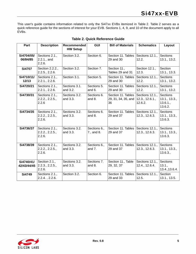
This user's guide contains information related to only the Si47xx EVBs itemized in Table 2. Table 2 serves as aquick reference guide for the sections of interest for your EVB. Sections 1, 4, 9, and 10 of the document apply to allEVBs.
Table 2. Quick Reference Guide
Part Description Recommended HW Setup
GUI Bill of Materials Schematics Layout
Si4704/05/06/84/85
Sections 2.1., 2.2.1., and 2.2.6.
Section 3.2. Section 6. Section 11. Tables 29 and 30
Sections 12.1., 12.2.
Sections 13.1., 13.2.
Si4707 Section 2.2.2., 2.2.5., 2.2.6.
Section 3.2. Section 7. Section 11., Tables 29 and 31
Section 12.1., 12.3.
Section 13.1., 13.3.
Si4710/11/12/13
Sections 2.1., 2.2.1., 2.2.6.
Section 3.1. Section 5. Section 11. Tables 29 and 30
Sections 12.1., 12.2.
Sections 13.1., 13.2.
Si4720/21 Sections 2.1., 2.2.1., 2.2.6.
Sections 3.1. and 3.2.
Sections 5. and 6.
Section 11. Tables 29 and 30
Sections 12.1., 12.2.
Sections 13.1., 13.2.
Si4730/31 Sections 2.1., 2.2.2., 2.2.5., 2.2.6
Sections 3.2. and 3.3.
Sections 6. and 8.
Section 11. Tables 29, 31, 34, 35, and 36
Sections 12.1., 12.3., 12.6.1., 12.6.2.
Sections 13.1., 13.3., 13.6.1., 13.6.2.
Si4734/35 Sections 2.1., 2.2.2., 2.2.5., 2.2.6.
Sections 3.2. and 3.3.
Sections 6. and 8.
Section 11. Tables 29 and 37
Sections 12.1., 12.3., 12.6.3.
Sections 13.1., 13.3., 13.6.3.
Si4736/37 Sections 2.1., 2.2.2., 2.2.5., 2.2.6.
Sections 3.2. and 3.3.
Sections 6., 7., and 8.
Section 11. Tables 29 and 37
Sections 12.1., 12.3., 12.6.3.
Sections 13.1., 13.3., 13.6.3.
Si4738/39 Sections 2.1., 2.2.2., 2.2.5., 2.2.6.
Sections 3.2. and 3.3.
Sections 6., and 7.
Section 11. Tables 29 and 37
Sections 12.1., 12.3., 12.6.3.
Sections 13.1., 13.3., 13.6.3.,
Si4740/41/42/43/44/45
Section 2.1., 2.2.3., 2.2.5., 2.2.6.
Sections 3.2. and 3.3.
Sections 7. and 8.
Section 11., Table 29, 32, 37
Sections 12.1., 12.4., 12.6.4.
Sections 13.1., 13.4.,13.6.4.
Si4749 Sections 2.1., 2.2.4. , 2.2.6.
Section 3.2. Section 6. Section 11. Tables 29 and 33
Sections 12.1., 12.5.
Section 13.1., 13.5.
Si47xx-EVB
6 Rev. 0.8
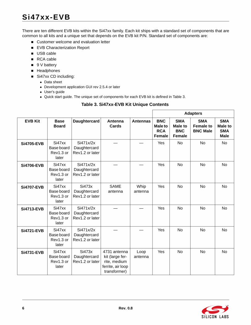
There are ten different EVB kits within the Si47xx family. Each kit ships with a standard set of components that arecommon to all kits and a unique set that depends on the EVB kit P/N. Standard set of components are:
Customer welcome and evaluation letter
EVB Characterization Report
USB cable
RCA cable
9 V battery
Headphones
Si47xx CD including:Data sheetDevelopment application GUI rev 2.5.4 or laterUser's guideQuick start guide. The unique set of components for each EVB kit is defined in Table 3.
Table 3. Si47xx-EVB Kit Unique Contents
Adapters
EVB Kit Base Board
Daughtercard Antenna Cards
Antennas BNC Male to
RCA Female
SMA Male to
BNC Female
SMA Female to BNC Male
SMA Male to
SMA Male
Si4705-EVB Si47xx Base board Rev1.3 or
later
Si471x/2x Daughtercard Rev1.2 or later
— — Yes No No No
Si4706-EVB Si47xx Base board Rev1.3 or
later
Si471x/2x Daughtercard Rev1.2 or later
— — Yes No No No
Si4707-EVB Si47xx Base board Rev1.3 or
later
Si473x Daughtercard Rev1.2 or later
SAME antenna
Whip antenna
Yes No No No
Si4713-EVB Si47xx Base board Rev1.3 or
later
Si471x/2x Daughtercard Rev1.2 or later
— — Yes No No No
Si4721-EVB Si47xx Base board Rev1.3 or
later
Si471x/2x Daughtercard Rev1.2 or later
— — Yes No No No
Si4731-EVB Si47xx Base board Rev1.3 or
later
Si473x Daughtercard Rev1.2 or later
4731 antenna kit (large fer-rite, medium
ferrite, air loop transformer)
Loop antenna
Yes No No No
Si47xx-EVB
Rev. 0.8 7
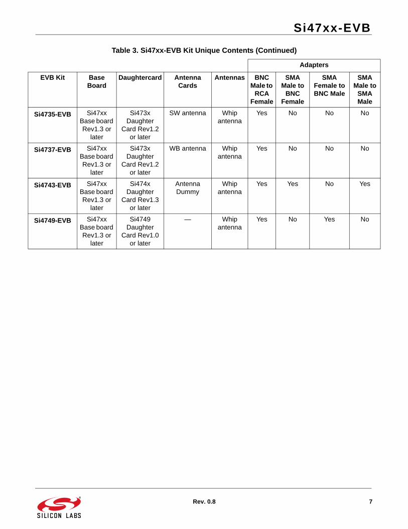
Si4735-EVB Si47xx Base board Rev1.3 or
later
Si473x Daughter
Card Rev1.2 or later
SW antenna Whip antenna
Yes No No No
Si4737-EVB Si47xx Base board Rev1.3 or
later
Si473x Daughter
Card Rev1.2 or later
WB antenna Whip antenna
Yes No No No
Si4743-EVB Si47xx Base board Rev1.3 or
later
Si474x Daughter
Card Rev1.3 or later
Antenna Dummy
Whip antenna
Yes Yes No Yes
Si4749-EVB Si47xx Base board Rev1.3 or
later
Si4749 Daughter
Card Rev1.0 or later
— Whip antenna
Yes No Yes No
Table 3. Si47xx-EVB Kit Unique Contents (Continued)
Adapters
EVB Kit Base Board
Daughtercard Antenna Cards
Antennas BNC Male to
RCA Female
SMA Male to
BNC Female
SMA Female to BNC Male
SMA Male to
SMA Male
Si47xx-EVB
8 Rev. 0.8
2. Description
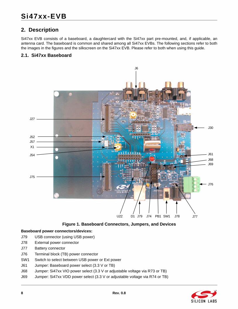
Si47xx EVB consists of a baseboard, a daughtercard with the Si47xx part pre-mounted, and, if applicable, anantenna card. The baseboard is common and shared among all Si47xx EVBs. The following sections refer to boththe images in the figures and the silkscreen on the Si47xx EVB. Please refer to both when using this guide.
2.1. Si47xx Baseboard
Figure 1. Baseboard Connectors, Jumpers, and Devices
Baseboard power connectors/devices:
J79 USB connector (using USB power)
J78 External power connector
J77 Battery connector
J76 Terminal block (TB) power connector
SW1 Switch to select between USB power or Ext power
J61 Jumper: Baseboard power select (3.3 V or TB)
J68 Jumper: Si47xx VIO power select (3.3 V or adjustable voltage via R73 or TB)
J69 Jumper: Si47xx VDD power select (3.3 V or adjustable voltage via R74 or TB)
J79 SW1 J78
J76
J74 PB1
J69J68
J61
J30
J6
J52
X1
J54
J57
J27
J75
U22 D1 J77
Si47xx-EVB
Rev. 0.8 9
Baseboard audio I/O connectors:
J6 RCA output
J30 Line outputNote: Line output will not be supported on new EVBs as of February 14, 2011.
Baseboard clock connectors/devices:
X1 32.768 kHz crystal oscillator
J52 Solder bump: select internal RCLK from oscillator
J54 Ext RCLK SMA connector input
J57 Jumper: Enable or Disable Int RCLK
Baseboard MCU connectors/devices:
U22 C8051F342 MCU
J79 USB connector to communicate with the MCU
J74 JTAG connector for the MCU
PB1 Push button to reset the MCU
D1 LED to confirm power supply to the MCU
Baseboard to Daughtercard connectors:
J27 Si47xx daughtercard connector
J75 Expansion card connector (reserved)
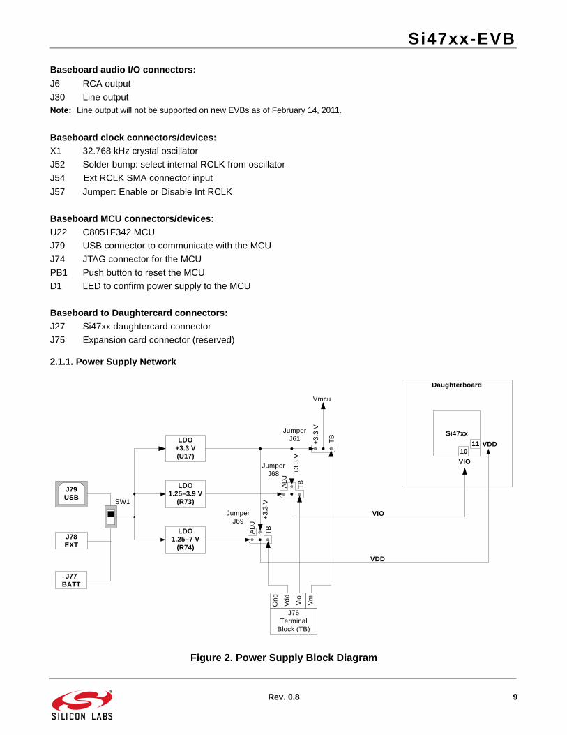
2.1.1. Power Supply Network
Figure 2. Power Supply Block Diagram
SW1
J78EXT
LDO1.25–3.9 V
(R73)
LDO1.25–7 V
(R74)
JumperJ68
JumperJ69
Daughterboard
Si47xx
VIO
1011 VDD
AD
J
TB
+3.
3 V
LDO+3.3 V(U17)
J79USB
J76Terminal
Block (TB)
Gnd
Vdd Vio
Vm
AD
J
+3.
3 V
TB
+3
.3 V
TB
Vmcu
JumperJ61
VIO
VDD
J77BATT
Si47xx-EVB
10 Rev. 0.8
The Si47xx EVB can be powered using one of the following power supply options:
1. USB power supply via J79
2. External dc (Ext DC) power supply via power jack J78 or battery via J77
3. Three separate power supplies (Vdd, Vio, Vmcu) via terminal block J76
The EVB has three supply rails: Vdd, Vio, and Vmcu. Vdd and Vio are routed directly to the daughtercard to powerthe Vdd and Vio pins on the Si47xx chip, while Vmcu is used to power the baseboard.
The external dc power supply and battery should not be connected simultaneously. Refer to Section 9. "Using theEVB with a 9 V Battery‚" on page 109 for more information.
USB Power Supply & EXT DC Power Supply
Switch SW1 is used to select between the USB power supply and Ext dc power supply.
The USB power supply or the Ext dc power supply can be configured in one of the following two modes:
1. Fixed +3.3 V
2. Adjustable Vdd and Vio
Fixed +3.3 V
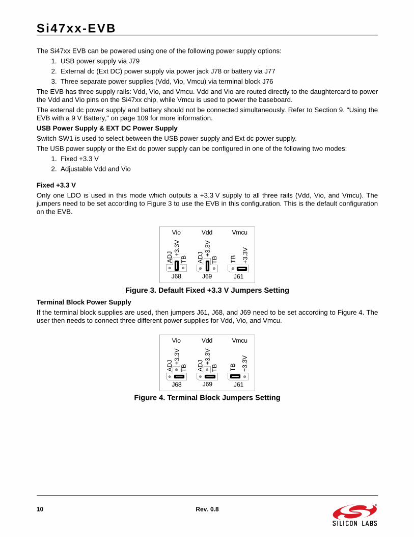
Only one LDO is used in this mode which outputs a +3.3 V supply to all three rails (Vdd, Vio, and Vmcu). Thejumpers need to be set according to Figure 3 to use the EVB in this configuration. This is the default configurationon the EVB.
Figure 3. Default Fixed +3.3 V Jumpers Setting
Terminal Block Power Supply
If the terminal block supplies are used, then jumpers J61, J68, and J69 need to be set according to Figure 4. Theuser then needs to connect three different power supplies for Vdd, Vio, and Vmcu.
Figure 4. Terminal Block Jumpers Setting
J69J68 J61
AD
J +3
.3V
TB
AD
J +3.
3VT
B
+3.
3V
TB
Vio Vdd Vmcu
AD
J +3.
3VT
B
+3.
3V
TB
AD
J +3.
3VT
B
J69J68 J61
Vio Vdd Vmcu
Si47xx-EVB
Rev. 0.8 11
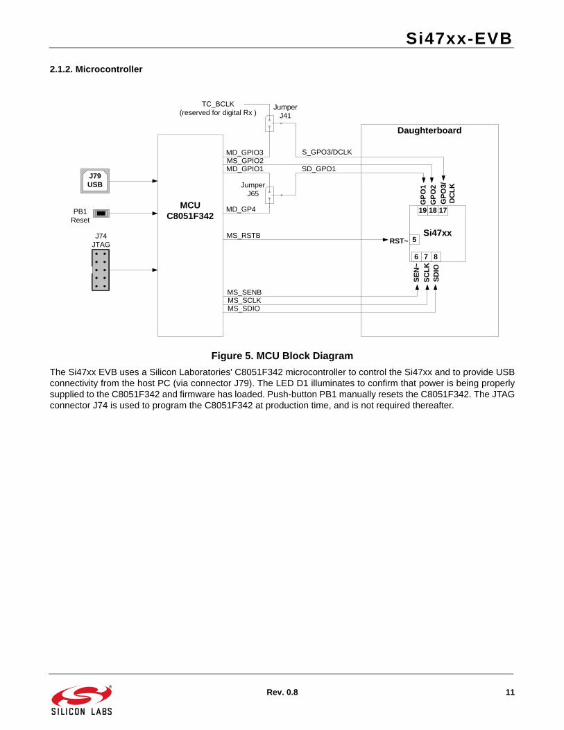
2.1.2. Microcontroller
Figure 5. MCU Block Diagram
The Si47xx EVB uses a Silicon Laboratories' C8051F342 microcontroller to control the Si47xx and to provide USBconnectivity from the host PC (via connector J79). The LED D1 illuminates to confirm that power is being properlysupplied to the C8051F342 and firmware has loaded. Push-button PB1 manually resets the C8051F342. The JTAGconnector J74 is used to program the C8051F342 at production time, and is not required thereafter.
MCUC8051F342
Si47xx
SE
N~
6 7 8
5
19 18 17
SC
LK
SD
IO
GP
O1
GP
O2
GP
O3/
DC
LK
RST~
MS_SENB
MS_RSTB
MS_SCLKMS_SDIO
S_GPO3/DCLKMS_GPIO2
SD_GPO1
Daughterboard
MD_GPIO3
TC_BCLK(reserved for digital Rx )
JumperJ41
MD_GPIO1
MD_GP4
J74JTAG
PB1Reset
J79USB Jumper
J65
Si47xx-EVB
12 Rev. 0.8
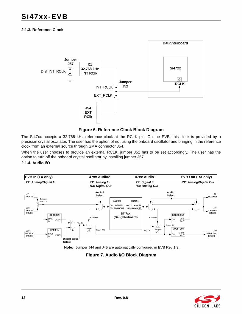
2.1.3. Reference Clock
Figure 6. Reference Clock Block Diagram
The Si47xx accepts a 32.768 kHz reference clock at the RCLK pin. On the EVB, this clock is provided by aprecision crystal oscillator. The user has the option of not using the onboard oscillator and bringing in the referenceclock from an external source through SMA connector J54.
When the user chooses to provide an external RCLK, jumper J52 has to be set accordingly. The user has theoption to turn off the onboard crystal oscillator by installing jumper J57.
2.1.4. Audio I/O
Figure 7. Audio I/O Block Diagram
Daughterboard
Si47xx
RCLK9
X132.768 kHzINT RClk
JumperJ52
J54EXT RClk
JumperJ57
DIS_INT_RCLK
INT_RCLK
EXT_RCLK
Note: Jumper J44 and J45 are automatically configured in EVB Rev 1.3.
JumperJ5&J13
EVB In (TX only) 47xx Audio2 47xx Audio1 EVB Out (RX only)
1
0
0
1
CODEC OUT
DIN LINE OUT
CODEC IN
LINE IN
DOUT
S/PDIF IN
SPDIF IN
DOUT
S/PDIF OUT
DINSPDIF
OUT
0
1
0
1
JumperJ45
TX: Analog/Digital In TX: Analog In TX: Digital In RX: Analog/Digital OutRX: Digital Out RX: Analog Out
AUDIO2
To_TX
From_RX
AUDIO1
From_RX
To_TX JumperJ44
RCA In
Line In(white)
SPDIF In(white)
RCA Out
Line Out(black)
SPDIF Out(black)
Si47xx(Daughterboard)
LIN/ DFS2
RIN/ DOUTLOUT/ DFS1
ROUT/ DIN
14
13
AUDIO1AUDIO2
15
16
J7
J19
J19
J6
J30
J30
Audio2 Select
Audio1Select
Digital Input Select
Si47xx-EVB
Rev. 0.8 13
The EVB supports three different kinds of configurations for the FM transmitter:
Analog In to Analog In
Analog In to Digital In
Digital In to Digital In
Analog In to Analog In: This configuration provides a way for the user to evaluate the analog audio input for FMtransmission.
The input to the EVB is an analog audio provided via the RCA input connector J7 or LINE In connector J19 (white).Jumpers J5 and J13 are set to RCA input by default. The user has to change this jumper accordingly if LINE In isbeing used. Then the analog audio input is routed directly through a switch to the Si47xx Rin/Lin inputs pin 15 and16 (Audio2).
Analog In to Digital In: This configuration provides a way for the user to evaluate the Si47xx digital audio input forFM transmission using an analog audio input.
The input to the EVB is an analog audio provided via the RCA input connector J7 or LINE In connector J19 (white).Jumpers J5 and J13 are set to RCA input by default. The user has to change this jumper accordingly if LINE In isbeing used. Then the analog audio input is converted by CODEC U10 to a serial audio digital data before it isrouted to the Si47xx digital audio input DIO and DFS pin 13 and 14 (Audio1). The DCLK input is routed to theGPO3/DCLK pin 17. Make sure that jumper J41 is set to DCLK to ensure proper operation.
Digital In to Digital In: This configuration provides a way for the user to evaluate the Si47xx digital audio input forFM transmission using S/PDIF digital audio commonly found in sound cards.
The input to the EVB is a digital S/PDIF data provided via the S/PDIF In connector J19 (white). The digital S/PDIFinput is converted by S/PDIF Translator U9 to a serial audio digital data before it is routed to the Si47xx digitalaudio input DIO and DFS pin 13 and 14 (Audio1). The DCLK input is routed to the GPO3/DCLK pin 17. Make surethat jumper J41 is set to DCLK to ensure proper operation.
Note: Digital in through J19 will not be supported on new EVBs as of February 14, 2011.
The EVB supports three different kinds of configurations for the FM receiver:
Analog Out to Analog Out
Digital Out to Digital and Analog Out
Dual Output (Digital and Analog Out)
Analog Out to Analog Out: This configuration provides a way for the user to evaluate the analog audio output forreceiver operation. The output of the Si47xx is routed to RCA output connector J6 and Line output connector J30.
Digital Out to Digital and Analog Out: This configuration provides a way for the user to evaluate the digital audiooutput for FM and AM receive using either S/PDIF digital audio or analog audio through the onboard CODEC. TheSi47xx digital audio out is routed through the S/PDIF translator µ9 to S/PDIF output connector J30 and routedthrough the CODEC to RCA output connector J6 and line output connector J30.
Note: Digital output through J30 will not be supported on new EVBs as of February 14, 2011.
Dual Output (Digital and Analog Out): This configuration provides a way for the user to evaluate the analogaudio out and digital audio using S/PDIF digital audio for FM and AM. The analog output of the Si47xx is routed toRCA output connector J6 and line output connector J30 and the digital audio out is routed through the S/PDIFtranslator to S/PDIF output connector J30.
Note: Digital output through J30 will not be supported on new EVBs as of February 14, 2011.

Si47xx-EVB
14 Rev. 0.8
IMPORTANT: Jumper Settings
Because of the many possibilities available to configure the EVB, ensure that these four jumpers are setaccordingly:
1. J41: GPO3/DCLK setting
2. J44: TX/RX setting for Audio1 I/O (automatically set by the GUI for baseboard 1.3 and later)
3. J45: TX/RX setting for Audio2 I/O (automatically set by the GUI for baseboard 1.3 and later)
4. J5, J13: Analog Audio Source, RCA or Line In
J41: GPO3/DCLK Setting
Upper—DCLK digital audio clock
Lower—GPO3 digital control signal
For configuring the Si47xx digital audio input, make sure that the jumper is set in the Upper position so that theDCLK signal will be routed to the Si47xx.
J44: TX/RX Setting for Audio1 I/O (automatically set by the GUI for baseboard 1.3 and later)
Upper—Audio1 is set to FM transmit (pin 13 and 14 will be the digital audio input).
Lower—Audio1 is set for FM receive (pin 13 and 14 will be analog/digital audio output).
J45: TX/RX Setting for Audio2 I/O (automatically set by the GUI for baseboard 1.3 and later)
Upper—Audio2 is set to FM transmit (pin 15 and 16 will be the analog/digital audio input).
Lower—Audio2 is set for FM receive (pin 15 and 16 will be the digital audio output).
J5, J13: Analog Audio Source, RCA or Line In
Upper—RCA inputs are used for analog audio source.
Lower—Line inputs are used for analog audio source.
Si47xx-EVB
Rev. 0.8 15
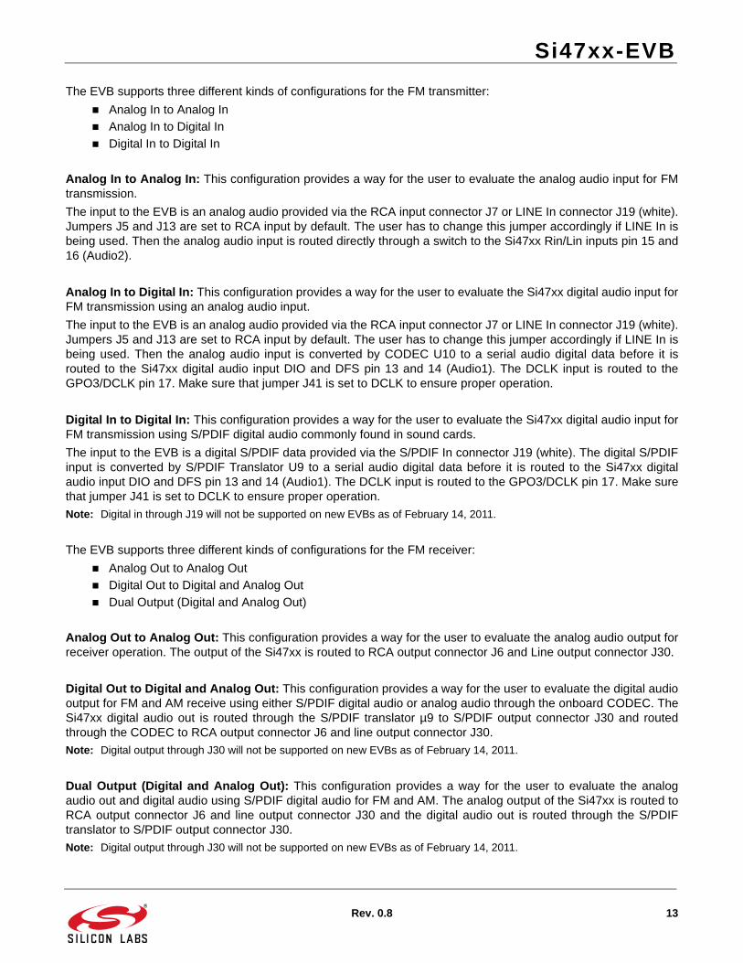
2.2. Si47xx Daughtercards2.2.1. Si471x/2x Daughtercard
Figure 8. Si471x/2x Daughtercard Connectors and Devices
Daughtercard Connectors and Components:
U1 Si472x FM Transceiver or Si470x FM Receiver or Si471x FM Transmitter
L2 Tuning Inductor
R2 0 resistor to connect FM TX output to 10 cm trace built-in antenna
C8 2 pF capacitor to connect FM TX output to J1 SMA connector
R4 50 termination resistor
J1 SMA connector for FM transmitter output or FM receiver input for embedded antenna
J2 Header for putting external antenna for FM transmitter or embedded antenna for FM receiver
J28 SMA connector for FM receiver input
J29 Headphone jack for FM receiver
Si47xx-EVB
16 Rev. 0.8
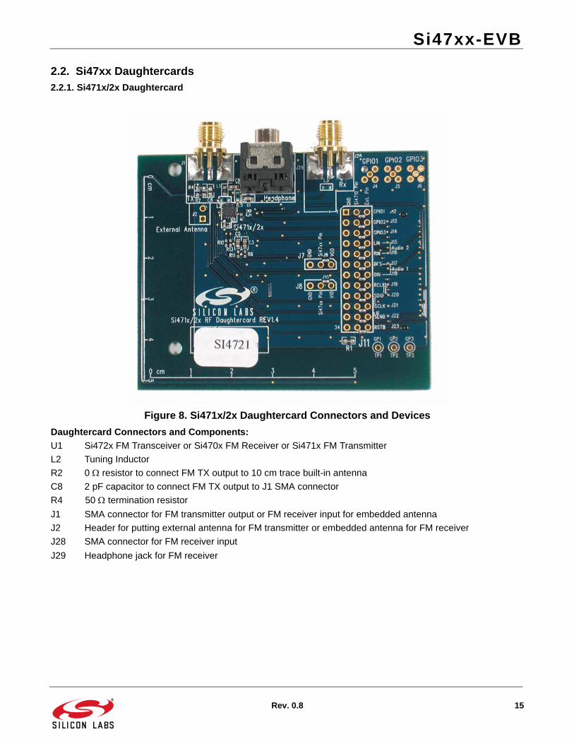
Figure 9. Fully Assembled Si471x/2x EVB
Si470x/1x/2x EVBs use Si471x/2x daughtercard with different population options depending on the individualSi470x/1x/2x part. Please refer to individual Bill of Materials for each board.
Si47xx-EVB
Rev. 0.8 17
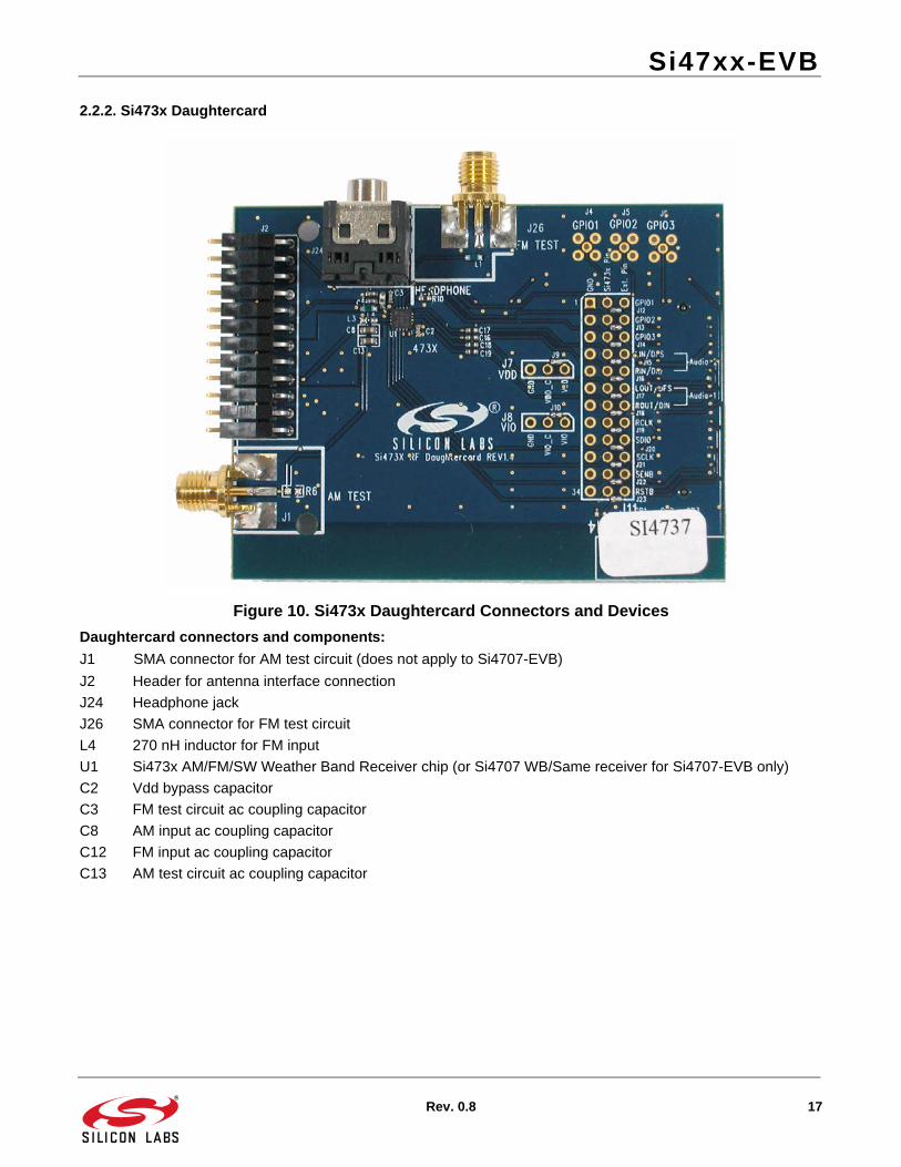
2.2.2. Si473x Daughtercard
Figure 10. Si473x Daughtercard Connectors and Devices
Daughtercard connectors and components:
J1 SMA connector for AM test circuit (does not apply to Si4707-EVB)
J2 Header for antenna interface connection
J24 Headphone jack
J26 SMA connector for FM test circuit
L4 270 nH inductor for FM input
U1 Si473x AM/FM/SW Weather Band Receiver chip (or Si4707 WB/Same receiver for Si4707-EVB only)
C2 Vdd bypass capacitor
C3 FM test circuit ac coupling capacitor
C8 AM input ac coupling capacitor
C12 FM input ac coupling capacitor
C13 AM test circuit ac coupling capacitor
Si47xx-EVB
18 Rev. 0.8
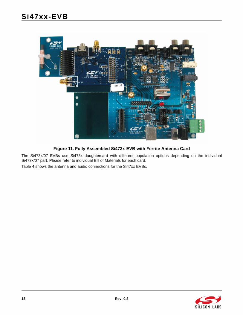
Figure 11. Fully Assembled Si473x-EVB with Ferrite Antenna Card
The Si473x/07 EVBs use Si473x daughtercard with different population options depending on the individualSi473x/07 part. Please refer to individual Bill of Materials for each card.
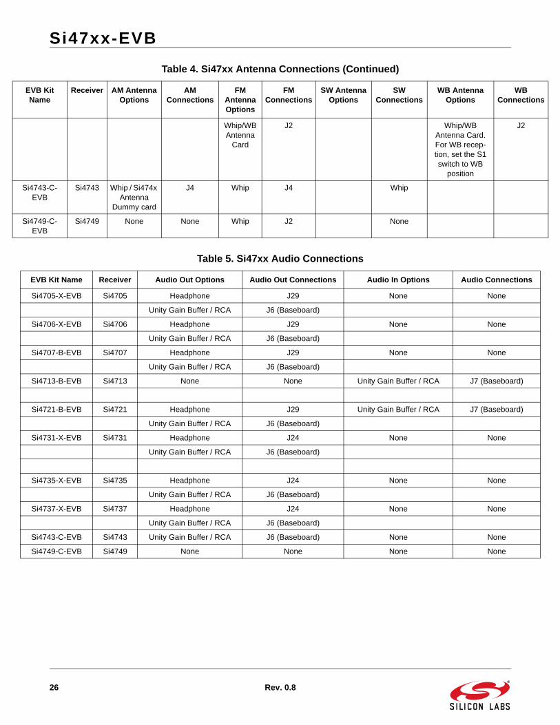
Table 4 shows the antenna and audio connections for the Si47xx EVBs.
Si47xx-EVB
Rev. 0.8 19
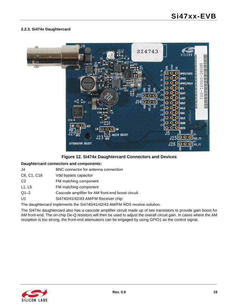
2.2.3. Si474x Daughtercard
Figure 12. Si474x Daughtercard Connectors and Devices
Daughtercard connectors and components:
J4 BNC connector for antenna connection
C6, C1, C18 Vdd bypass capacitor
C2 FM matching component
L1, L5 FM matching component
Q1–2 Cascode amplifier for AM front-end boost circuit.
U1 Si4740/41/42/43 AM/FM Receiver chip
The daughtercard implements the Si4740/41/42/43 AM/FM RDS receive solution.
The Si474x daughtercard also has a cascode amplifier circuit made up of two transistors to provide gain boost forAM front-end. The on-chip De-Q resistors will then be used to adjust the overall circuit gain. In cases where the AMreception is too strong, the front-end attenuators can be engaged by using GPIO1 as the control signal.
Si47xx-EVB
20 Rev. 0.8
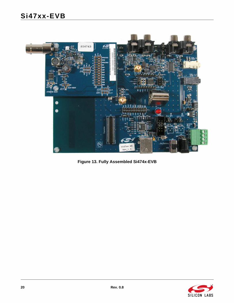
Figure 13. Fully Assembled Si474x-EVB
Si47xx-EVB
Rev. 0.8 21
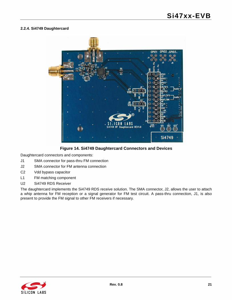
2.2.4. Si4749 Daughtercard
Figure 14. Si4749 Daughtercard Connectors and Devices
Daughtercard connectors and components:
J1 SMA connector for pass-thru FM connection
J2 SMA connector for FM antenna connection
C2 Vdd bypass capacitor
L1 FM matching component
U2 Si4749 RDS Receiver
The daughtercard implements the Si4749 RDS receive solution. The SMA connector, J2, allows the user to attacha whip antenna for FM reception or a signal generator for FM test circuit. A pass-thru connection, J1, is alsopresent to provide the FM signal to other FM receivers if necessary.
Si47xx-EVB
22 Rev. 0.8
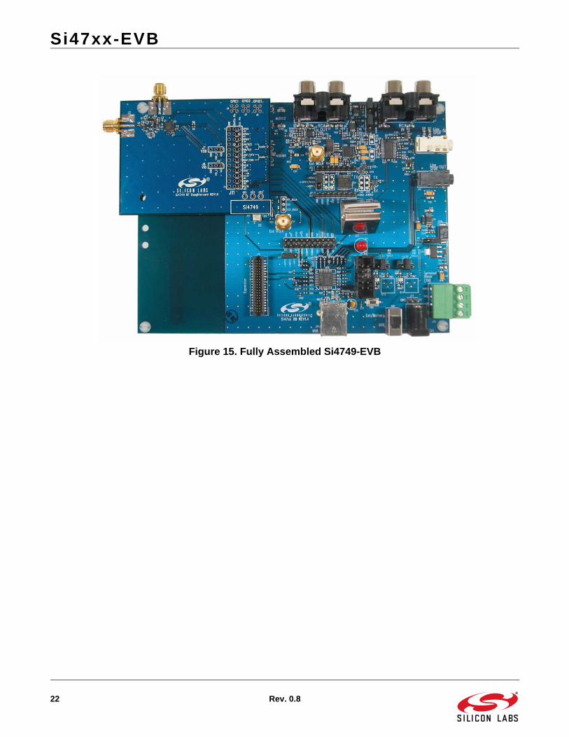
Figure 15. Fully Assembled Si4749-EVB
Si47xx-EVB
Rev. 0.8 23
2.2.5. Antenna Interfaces
2.2.5.1. AM Antenna Interface
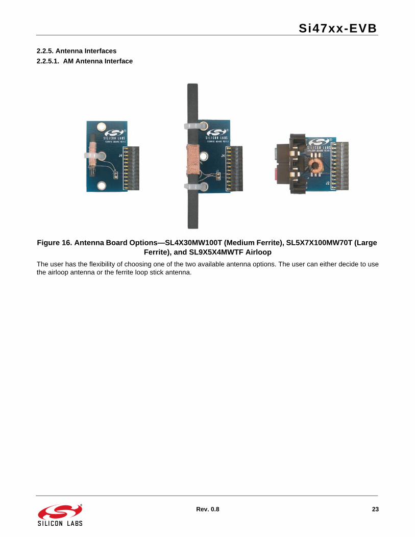
Figure 16. Antenna Board Options—SL4X30MW100T (Medium Ferrite), SL5X7X100MW70T (Large Ferrite), and SL9X5X4MWTF Airloop
The user has the flexibility of choosing one of the two available antenna options. The user can either decide to usethe airloop antenna or the ferrite loop stick antenna.
Si47xx-EVB
24 Rev. 0.8
2.2.5.2. SW and Weather Band Antenna Interfaces
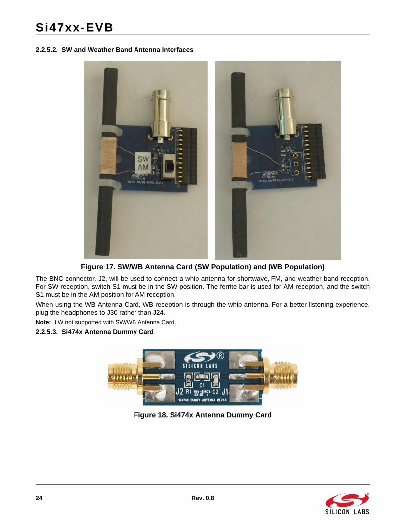
Figure 17. SW/WB Antenna Card (SW Population) and (WB Population)
The BNC connector, J2, will be used to connect a whip antenna for shortwave, FM, and weather band reception.For SW reception, switch S1 must be in the SW position. The ferrite bar is used for AM reception, and the switchS1 must be in the AM position for AM reception.
When using the WB Antenna Card, WB reception is through the whip antenna. For a better listening experience,plug the headphones to J30 rather than J24.
Note: LW not supported with SW/WB Antenna Card.
2.2.5.3. Si474x Antenna Dummy Card
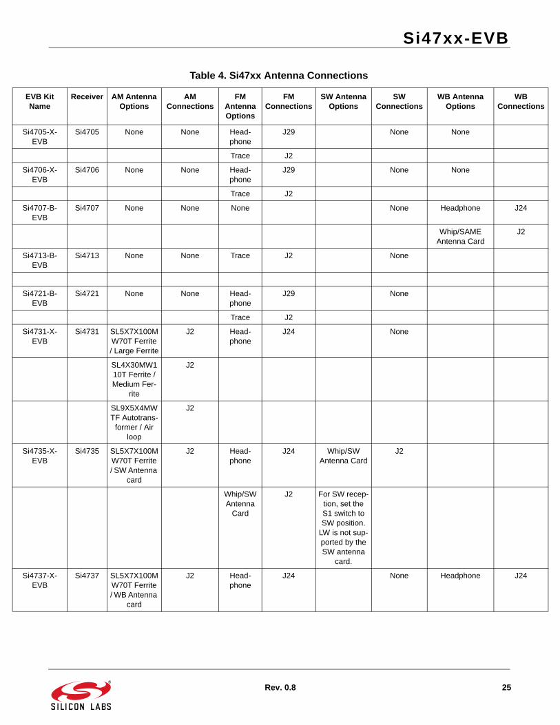
Figure 18. Si474x Antenna Dummy Card
Si47xx-EVB
Rev. 0.8 25
Table 4. Si47xx Antenna Connections
EVB Kit Name
Receiver AM Antenna Options
AM Connections
FM Antenna Options
FM Connections
SW Antenna Options
SW Connections
WB Antenna Options
WB Connections
Si4705-X-EVB
Si4705 None None Head-phone
J29 None None
Trace J2
Si4706-X-EVB
Si4706 None None Head-phone
J29 None None
Trace J2
Si4707-B-EVB
Si4707 None None None None Headphone J24
Whip/SAME Antenna Card
J2
Si4713-B-EVB
Si4713 None None Trace J2 None
Si4721-B-EVB
Si4721 None None Head-phone
J29 None
Trace J2
Si4731-X-EVB
Si4731 SL5X7X100MW70T Ferrite / Large Ferrite
J2 Head-phone
J24 None
SL4X30MW110T Ferrite / Medium Fer-
rite
J2
SL9X5X4MWTF Autotrans-
former / Air loop
J2
Si4735-X-EVB
Si4735 SL5X7X100MW70T Ferrite / SW Antenna
card
J2 Head-phone
J24 Whip/SW Antenna Card
J2
Whip/SW Antenna
Card
J2 For SW recep-tion, set the S1 switch to SW position.
LW is not sup-ported by the SW antenna
card.
Si4737-X-EVB
Si4737 SL5X7X100MW70T Ferrite / WB Antenna
card
J2 Head-phone
J24 None Headphone J24
Si47xx-EVB
26 Rev. 0.8
Whip/WB Antenna
Card
J2 Whip/WB Antenna Card. For WB recep-tion, set the S1 switch to WB
position
J2
Si4743-C-EVB
Si4743 Whip / Si474x Antenna
Dummy card
J4 Whip J4 Whip
Si4749-C-EVB
Si4749 None None Whip J2 None
Table 5. Si47xx Audio Connections
EVB Kit Name Receiver Audio Out Options Audio Out Connections Audio In Options Audio Connections
Si4705-X-EVB Si4705 Headphone J29 None None
Unity Gain Buffer / RCA J6 (Baseboard)
Si4706-X-EVB Si4706 Headphone J29 None None
Unity Gain Buffer / RCA J6 (Baseboard)
Si4707-B-EVB Si4707 Headphone J29 None None
Unity Gain Buffer / RCA J6 (Baseboard)
Si4713-B-EVB Si4713 None None Unity Gain Buffer / RCA J7 (Baseboard)
Si4721-B-EVB Si4721 Headphone J29 Unity Gain Buffer / RCA J7 (Baseboard)
Unity Gain Buffer / RCA J6 (Baseboard)
Si4731-X-EVB Si4731 Headphone J24 None None
Unity Gain Buffer / RCA J6 (Baseboard)
Si4735-X-EVB Si4735 Headphone J24 None None
Unity Gain Buffer / RCA J6 (Baseboard)
Si4737-X-EVB Si4737 Headphone J24 None None
Unity Gain Buffer / RCA J6 (Baseboard)
Si4743-C-EVB Si4743 Unity Gain Buffer / RCA J6 (Baseboard) None None
Si4749-C-EVB Si4749 None None None None
Table 4. Si47xx Antenna Connections (Continued)
EVB Kit Name
Receiver AM Antenna Options
AM Connections
FM Antenna Options
FM Connections
SW Antenna Options
SW Connections
WB Antenna Options
WB Connections
Si47xx-EVB
Rev. 0.8 27
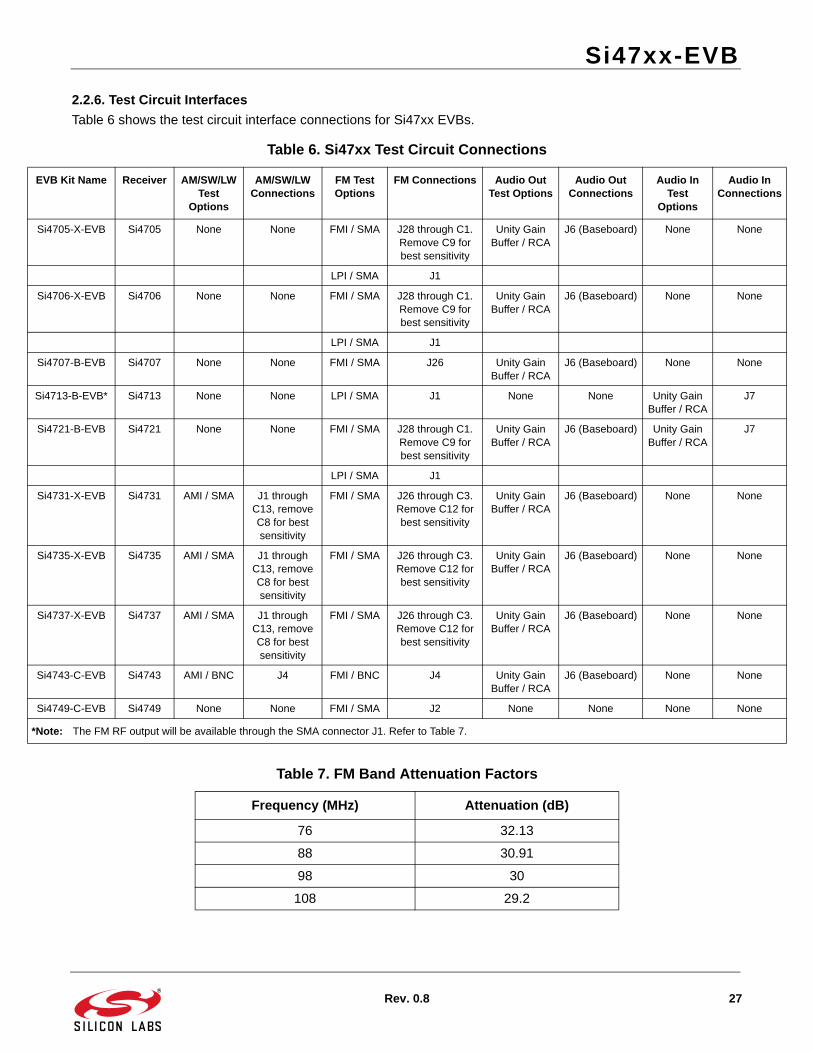
2.2.6. Test Circuit Interfaces
Table 6 shows the test circuit interface connections for Si47xx EVBs.
Table 6. Si47xx Test Circuit Connections
EVB Kit Name Receiver AM/SW/LW Test
Options
AM/SW/LW Connections
FM Test Options
FM Connections Audio Out Test Options
Audio Out Connections
Audio In Test
Options
Audio In Connections
Si4705-X-EVB Si4705 None None FMI / SMA J28 through C1. Remove C9 for best sensitivity
Unity Gain Buffer / RCA
J6 (Baseboard) None None
LPI / SMA J1
Si4706-X-EVB Si4706 None None FMI / SMA J28 through C1. Remove C9 for best sensitivity
Unity Gain Buffer / RCA
J6 (Baseboard) None None
LPI / SMA J1
Si4707-B-EVB Si4707 None None FMI / SMA J26 Unity Gain Buffer / RCA
J6 (Baseboard) None None
Si4713-B-EVB* Si4713 None None LPI / SMA J1 None None Unity Gain Buffer / RCA
J7
Si4721-B-EVB Si4721 None None FMI / SMA J28 through C1. Remove C9 for best sensitivity
Unity Gain Buffer / RCA
J6 (Baseboard) Unity Gain Buffer / RCA
J7
LPI / SMA J1
Si4731-X-EVB Si4731 AMI / SMA J1 through C13, remove C8 for best sensitivity
FMI / SMA J26 through C3. Remove C12 for best sensitivity
Unity Gain Buffer / RCA
J6 (Baseboard) None None
Si4735-X-EVB Si4735 AMI / SMA J1 through C13, remove C8 for best sensitivity
FMI / SMA J26 through C3. Remove C12 for best sensitivity
Unity Gain Buffer / RCA
J6 (Baseboard) None None
Si4737-X-EVB Si4737 AMI / SMA J1 through C13, remove C8 for best sensitivity
FMI / SMA J26 through C3. Remove C12 for best sensitivity
Unity Gain Buffer / RCA
J6 (Baseboard) None None
Si4743-C-EVB Si4743 AMI / BNC J4 FMI / BNC J4 Unity Gain Buffer / RCA
J6 (Baseboard) None None
Si4749-C-EVB Si4749 None None FMI / SMA J2 None None None None
*Note: The FM RF output will be available through the SMA connector J1. Refer to Table 7.
Table 7. FM Band Attenuation Factors
Frequency (MHz) Attenuation (dB)
76 32.13
88 30.91
98 30
108 29.2
Si47xx-EVB
28 Rev. 0.8
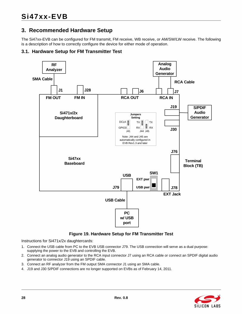
3. Recommended Hardware Setup
The Si47xx-EVB can be configured for FM transmit, FM receive, WB receive, or AM/SW/LW receive. The followingis a description of how to correctly configure the device for either mode of operation.
3.1. Hardware Setup for FM Transmitter Test
Figure 19. Hardware Setup for FM Transmitter Test
Instructions for Si471x/2x daughtercards:
1. Connect the USB cable from PC to the EVB USB connector J79. The USB connection will serve as a dual purpose: supplying the power to the EVB and controlling the EVB.
2. Connect an analog audio generator to the RCA input connector J7 using an RCA cable or connect an SPDIF digital audio generator to connector J19 using an SPDIF cable.
3. Connect an RF analyzer from the FM output SMA connector J1 using an SMA cable.4. J19 and J30 S/PDIF connections are no longer supported on EVBs as of February 14, 2011.
Si471x/2x Daughterboard
RFAnalyzer
Analog Audio
Generator
PC w/ USB
port
J28
RCA OUT
USB
FM IN
J6
J79
USB Cable
SMA CableRCA Cable
EXT pwr
USB pwr
EXT Jack
SW1
Terminal Block (TB)
J76
J78
Si47xxBaseboard
J1
FM OUT RCA IN
J7
J19
J30
S/PDIF Audio
Generator
J44 J45
JumpersSetting
J41
TX
RX
TX
RX
DCLK
GPIO3
Note: J44 and J45 are automatically configured in
EVB Rev1.3 and later
Si47xx-EVB
Rev. 0.8 29
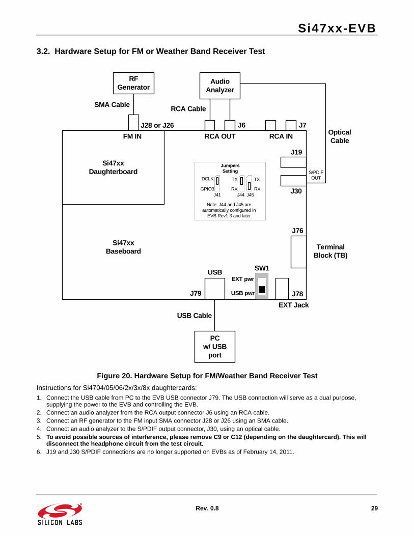
3.2. Hardware Setup for FM or Weather Band Receiver Test
Figure 20. Hardware Setup for FM/Weather Band Receiver Test
Instructions for Si4704/05/06/2x/3x/8x daughtercards:
1. Connect the USB cable from PC to the EVB USB connector J79. The USB connection will serve as a dual purpose, supplying the power to the EVB and controlling the EVB.
2. Connect an audio analyzer from the RCA output connector J6 using an RCA cable.3. Connect an RF generator to the FM input SMA connector J28 or J26 using an SMA cable.4. Connect an audio analyzer to the S/PDIF output connector, J30, using an optical cable.5. To avoid possible sources of interference, please remove C9 or C12 (depending on the daughtercard). This will
disconnect the headphone circuit from the test circuit. 6. J19 and J30 S/PDIF connections are no longer supported on EVBs as of February 14, 2011.
Si47xx Daughterboard
RFGenerator
AudioAnalyzer
PC w/ USB
port
J28 or J26
RCA OUT
USB
FM IN
J6
J79
USB Cable
SMA CableRCA Cable
EXT pwr
USB pwr
EXT Jack
SW1
Terminal Block (TB)
J76
J78
J44 J45
JumpersSetting
J41
TX
RX
TX
RX
DCLK
GPIO3
Note: J44 and J45 are automatically configured in
EVB Rev1.3 and later
Si47xxBaseboard
RCA IN
J7
J19
J30
Optical Cable
S/PDIF OUT
Si47xx-EVB
30 Rev. 0.8
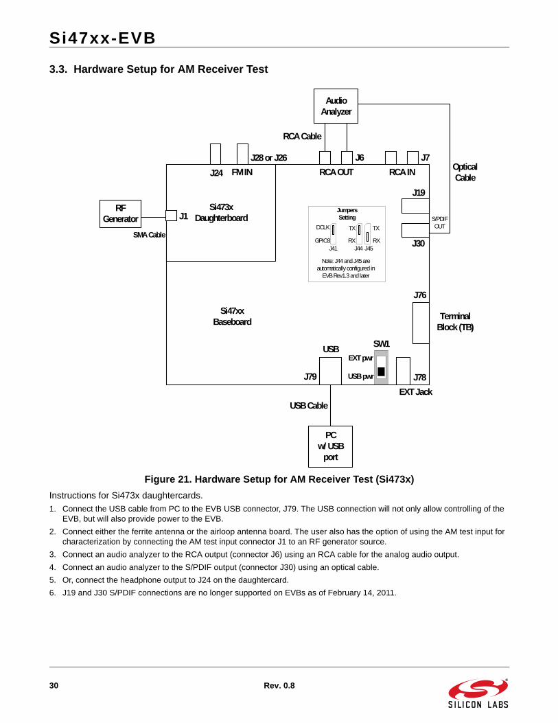
3.3. Hardware Setup for AM Receiver Test
Figure 21. Hardware Setup for AM Receiver Test (Si473x)
Instructions for Si473x daughtercards.
1. Connect the USB cable from PC to the EVB USB connector, J79. The USB connection will not only allow controlling of the EVB, but will also provide power to the EVB.
2. Connect either the ferrite antenna or the airloop antenna board. The user also has the option of using the AM test input for characterization by connecting the AM test input connector J1 to an RF generator source.
3. Connect an audio analyzer to the RCA output (connector J6) using an RCA cable for the analog audio output.
4. Connect an audio analyzer to the S/PDIF output (connector J30) using an optical cable.
5. Or, connect the headphone output to J24 on the daughtercard.
6. J19 and J30 S/PDIF connections are no longer supported on EVBs as of February 14, 2011.
Si473x Daughterboard
RFGenerator
AudioAnalyzer
PC w/ USB
port
J28 or J26
RCA OUT
USB
FM IN
J6
J79
USB Cable
SMA Cable
RCA Cable
EXT pwr
USB pwr
EXT Jack
SW1
Terminal Block (TB)
J76
J78
J44 J45
JumpersSetting
J41
TX
RX
TX
RX
DCLK
GPIO3
Note: J44 and J45 are automatically configured in
EVB Rev1.3 and later
Si47xxBaseboard
J24 RCA IN
J7
J19
J30
Optical Cable
S/PDIF OUT
J1
Si47xx-EVB
Rev. 0.8 31
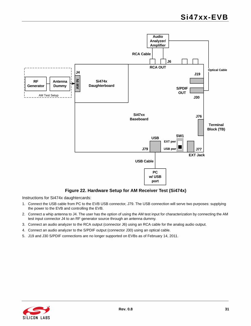
Figure 22. Hardware Setup for AM Receiver Test (Si474x)
Instructions for Si474x daughtercards:
1. Connect the USB cable from PC to the EVB USB connector, J79. The USB connection will serve two purposes: supplying the power to the EVB and controlling the EVB.
2. Connect a whip antenna to J4. The user has the option of using the AM test input for characterization by connecting the AM test input connector J4 to an RF generator source through an antenna dummy.
3. Connect an audio analyzer to the RCA output (connector J6) using an RCA cable for the analog audio output.
4. Connect an audio analyzer to the S/PDIF output (connector J30) using an optical cable.
5. J19 and J30 S/PDIF connections are no longer supported on EVBs as of February 14, 2011.
Si47xx Baseboard
Si474x Daughterboard
RF Generator
Audio Analyzer/Amplifier
PC w/ USB
port
RCA OUT
USB
J79
USB Cable
RCA Cable
EXT pwr
USB pwr
EXT Jack
SW1
Terminal Block (TB)
J76
J77
AM
IN
J6
J19
J30
S/PDIF OUT
Optical CableJ4
Antenna Dummy
AM Test Setup
Si47xx-EVB
32 Rev. 0.8
4. Getting Started
4.1. Software InstallationThe Si47xx Windows GUI (graphical user interface) software is designed for use with the Si47xx evaluation board(EVB). The GUI software revision number is available under HelpAbout.
The GUI software development program uses a host machine USB port to communicate with the Si47xx EVB andis tested for use with Windows XP, Windows 2000, and Windows 7.
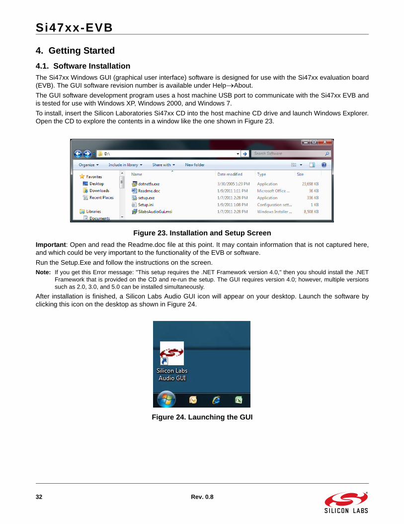
To install, insert the Silicon Laboratories Si47xx CD into the host machine CD drive and launch Windows Explorer.Open the CD to explore the contents in a window like the one shown in Figure 23.
Figure 23. Installation and Setup Screen
Important: Open and read the Readme.doc file at this point. It may contain information that is not captured here,and which could be very important to the functionality of the EVB or software.
Run the Setup.Exe and follow the instructions on the screen.
Note: If you get this Error message: "This setup requires the .NET Framework version 4.0," then you should install the .NETFramework that is provided on the CD and re-run the setup. The GUI requires version 4.0; however, multiple versionssuch as 2.0, 3.0, and 5.0 can be installed simultaneously.
After installation is finished, a Silicon Labs Audio GUI icon will appear on your desktop. Launch the software byclicking this icon on the desktop as shown in Figure 24.
Figure 24. Launching the GUI
Si47xx-EVB
Rev. 0.8 33
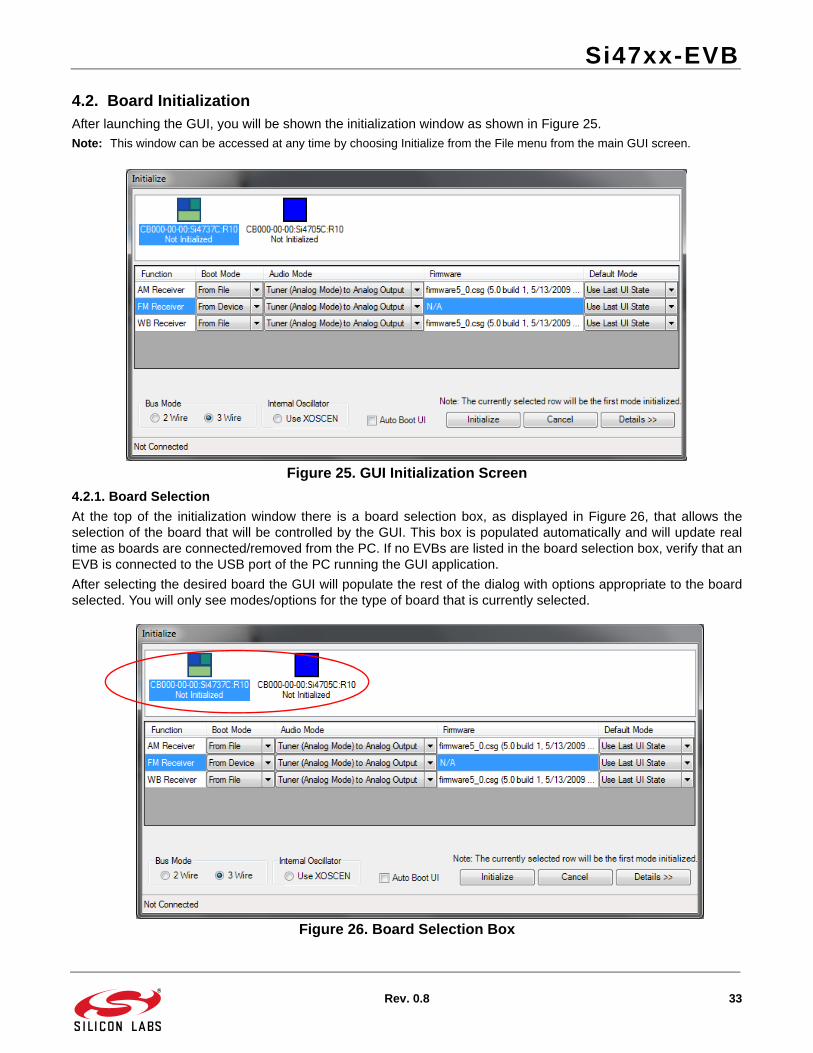
4.2. Board InitializationAfter launching the GUI, you will be shown the initialization window as shown in Figure 25.
Note: This window can be accessed at any time by choosing Initialize from the File menu from the main GUI screen.
Figure 25. GUI Initialization Screen
4.2.1. Board Selection
At the top of the initialization window there is a board selection box, as displayed in Figure 26, that allows theselection of the board that will be controlled by the GUI. This box is populated automatically and will update realtime as boards are connected/removed from the PC. If no EVBs are listed in the board selection box, verify that anEVB is connected to the USB port of the PC running the GUI application.
After selecting the desired board the GUI will populate the rest of the dialog with options appropriate to the boardselected. You will only see modes/options for the type of board that is currently selected.
Figure 26. Board Selection Box
Si47xx-EVB
34 Rev. 0.8
4.2.2. Board Discovery Bus Mode
The initialize process can be configured to use either 2-wire or 3-wire bus mode. This can be configured byselecting File Board Discovery Bus Mode.
This feature is useful when using the Silabs EVB and GUI to control a prototype that is designed to use one busmode only.
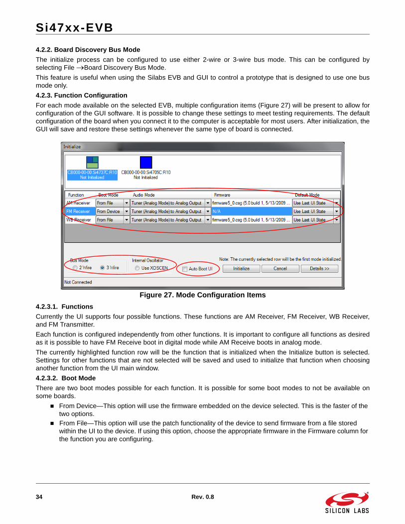
4.2.3. Function Configuration
For each mode available on the selected EVB, multiple configuration items (Figure 27) will be present to allow forconfiguration of the GUI software. It is possible to change these settings to meet testing requirements. The defaultconfiguration of the board when you connect it to the computer is acceptable for most users. After initialization, theGUI will save and restore these settings whenever the same type of board is connected.
Figure 27. Mode Configuration Items
4.2.3.1. Functions
Currently the UI supports four possible functions. These functions are AM Receiver, FM Receiver, WB Receiver,and FM Transmitter.
Each function is configured independently from other functions. It is important to configure all functions as desiredas it is possible to have FM Receive boot in digital mode while AM Receive boots in analog mode.
The currently highlighted function row will be the function that is initialized when the Initialize button is selected.Settings for other functions that are not selected will be saved and used to initialize that function when choosinganother function from the UI main window.
4.2.3.2. Boot Mode
There are two boot modes possible for each function. It is possible for some boot modes to not be available onsome boards.
From Device—This option will use the firmware embedded on the device selected. This is the faster of the two options.
From File—This option will use the patch functionality of the device to send firmware from a file stored within the UI to the device. If using this option, choose the appropriate firmware in the Firmware column for the function you are configuring.
Si47xx-EVB
Rev. 0.8 35
4.2.3.3. Default Mode
There are two or more default modes possible for each function.
Use Last UI State: When selected, the GUI will restore all settings on the device to the previous settings configured in the GUI the last time it was closed.
Use Chip Defaults: When selected, the GUI will use the settings that were default in the firmware on the device. Only properties related to the correct setting of RCLK (such as frequency and prescaling) and initial tuning (such as frequency) will be changed. If an error occurs during initialization of a function, choose this setting to default the GUI settings back to the chip defaults.
Saved Configuration States: If you have previously saved or imported any configuration states, they will be listed by name. When one of these is selected, the GUI will restore all settings on the device to the previously saved settings.
4.2.3.4. Audio Mode
This option allows the user to change between Analog or Digital modes if the board connected supports digital.Sections 2.1.4, 5, 6, and 7 each document the possible settings in more detail depending on what function is beingconfigured.
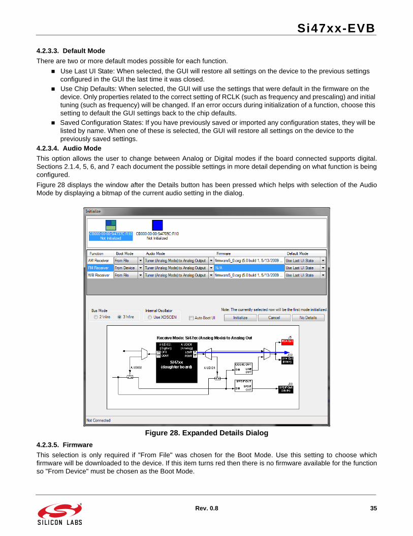
Figure 28 displays the window after the Details button has been pressed which helps with selection of the AudioMode by displaying a bitmap of the current audio setting in the dialog.
Figure 28. Expanded Details Dialog
4.2.3.5. Firmware
This selection is only required if "From File" was chosen for the Boot Mode. Use this setting to choose whichfirmware will be downloaded to the device. If this item turns red then there is no firmware available for the functionso "From Device" must be chosen as the Boot Mode.
Si47xx-EVB
36 Rev. 0.8
4.2.3.6. Bus Mode
This setting affects all functions that are configured. It allows the device to be booted either in 2-wire or 3-wiremode.
4.2.3.7. Internal Oscillator
When the "Use XOSCEN" is enabled and the board is configured to use the crystal oscillator, the GUI will boot thedevice using the crystal oscillator. This option is only available on devices that support the crystal oscillator option.
4.2.3.8. Auto Boot when UI Opened and only One Board is Connected
When this item is selected, the GUI, when launched, will automatically boot the board if the same board isconnected. If more than one board is connected, the GUI will display the initialization dialog to allow selection ofthe board to initialize.
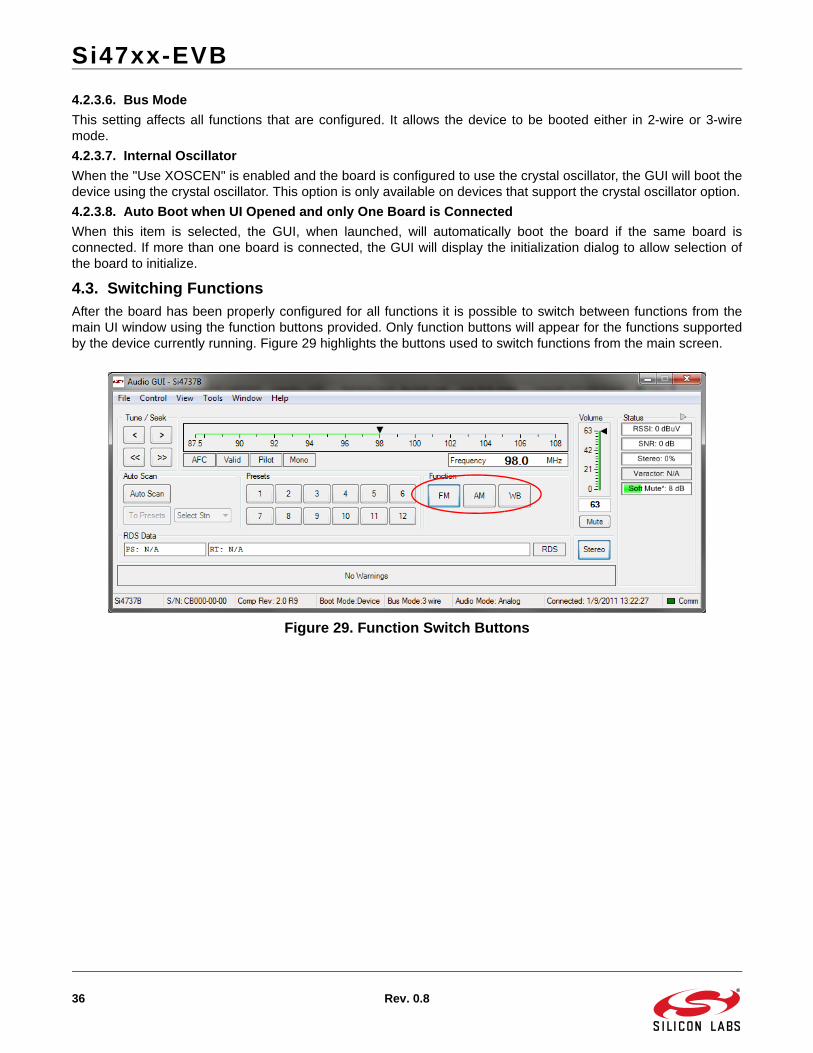
4.3. Switching FunctionsAfter the board has been properly configured for all functions it is possible to switch between functions from themain UI window using the function buttons provided. Only function buttons will appear for the functions supportedby the device currently running. Figure 29 highlights the buttons used to switch functions from the main screen.
Figure 29. Function Switch Buttons
Si47xx-EVB
Rev. 0.8 37
4.4. State ManagementOnce the part has been initialized, a State Management option becomes available in the File Menu. This GUIfeature allows the user to save, retrieve, load, and delete the configuration state which contains the propertyvalues.
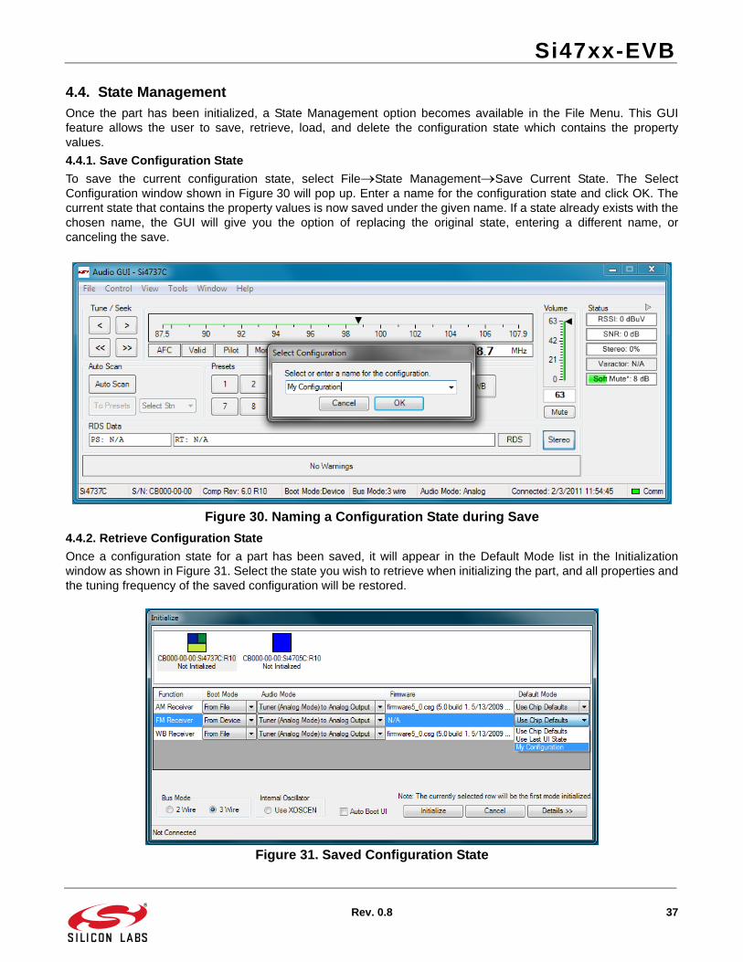
4.4.1. Save Configuration State
To save the current configuration state, select FileState ManagementSave Current State. The SelectConfiguration window shown in Figure 30 will pop up. Enter a name for the configuration state and click OK. Thecurrent state that contains the property values is now saved under the given name. If a state already exists with thechosen name, the GUI will give you the option of replacing the original state, entering a different name, orcanceling the save.
Figure 30. Naming a Configuration State during Save
4.4.2. Retrieve Configuration State
Once a configuration state for a part has been saved, it will appear in the Default Mode list in the Initializationwindow as shown in Figure 31. Select the state you wish to retrieve when initializing the part, and all properties andthe tuning frequency of the saved configuration will be restored.
Figure 31. Saved Configuration State
Si47xx-EVB
38 Rev. 0.8
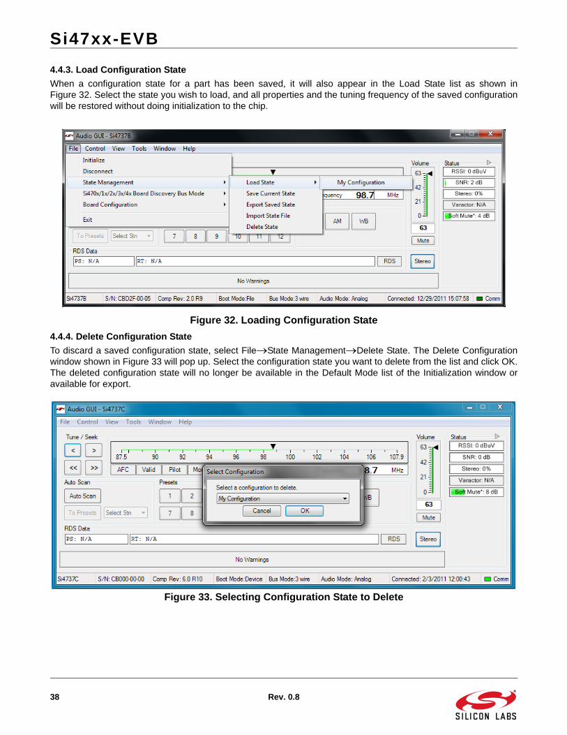
4.4.3. Load Configuration State
When a configuration state for a part has been saved, it will also appear in the Load State list as shown inFigure 32. Select the state you wish to load, and all properties and the tuning frequency of the saved configurationwill be restored without doing initialization to the chip.
Figure 32. Loading Configuration State
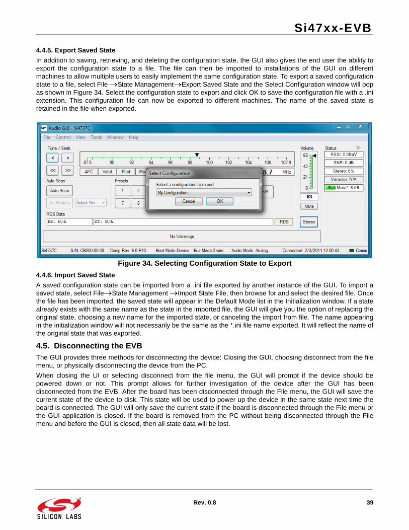
4.4.4. Delete Configuration State
To discard a saved configuration state, select FileState ManagementDelete State. The Delete Configurationwindow shown in Figure 33 will pop up. Select the configuration state you want to delete from the list and click OK.The deleted configuration state will no longer be available in the Default Mode list of the Initialization window oravailable for export.
Figure 33. Selecting Configuration State to Delete
Si47xx-EVB
Rev. 0.8 39
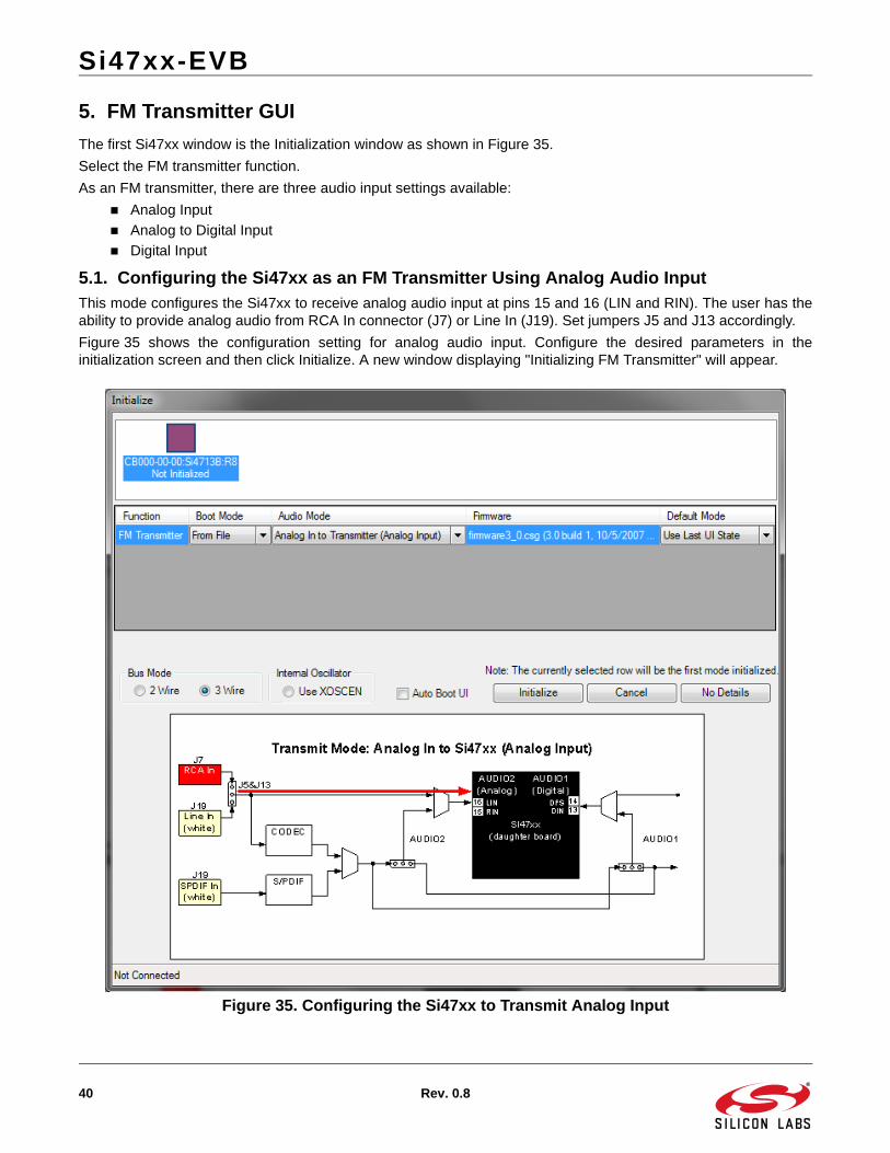
4.4.5. Export Saved State
In addition to saving, retrieving, and deleting the configuration state, the GUI also gives the end user the ability toexport the configuration state to a file. The file can then be imported to installations of the GUI on differentmachines to allow multiple users to easily implement the same configuration state. To export a saved configurationstate to a file, select File State ManagementExport Saved State and the Select Configuration window will popas shown in Figure 34. Select the configuration state to export and click OK to save the configuration file with a .iniextension. This configuration file can now be exported to different machines. The name of the saved state isretained in the file when exported.
Figure 34. Selecting Configuration State to Export
4.4.6. Import Saved State
A saved configuration state can be imported from a .ini file exported by another instance of the GUI. To import asaved state, select FileState Management Import State File, then browse for and select the desired file. Oncethe file has been imported, the saved state will appear in the Default Mode list in the Initialization window. If a statealready exists with the same name as the state in the imported file, the GUI will give you the option of replacing theoriginal state, choosing a new name for the imported state, or canceling the import from file. The name appearingin the initialization window will not necessarily be the same as the *.ini file name exported. It will reflect the name ofthe original state that was exported.
4.5. Disconnecting the EVBThe GUI provides three methods for disconnecting the device: Closing the GUI, choosing disconnect from the filemenu, or physically disconnecting the device from the PC.
When closing the UI or selecting disconnect from the file menu, the GUI will prompt if the device should bepowered down or not. This prompt allows for further investigation of the device after the GUI has beendisconnected from the EVB. After the board has been disconnected through the File menu, the GUI will save thecurrent state of the device to disk. This state will be used to power up the device in the same state next time theboard is connected. The GUI will only save the current state if the board is disconnected through the File menu orthe GUI application is closed. If the board is removed from the PC without being disconnected through the Filemenu and before the GUI is closed, then all state data will be lost.
Si47xx-EVB
40 Rev. 0.8
5. FM Transmitter GUI
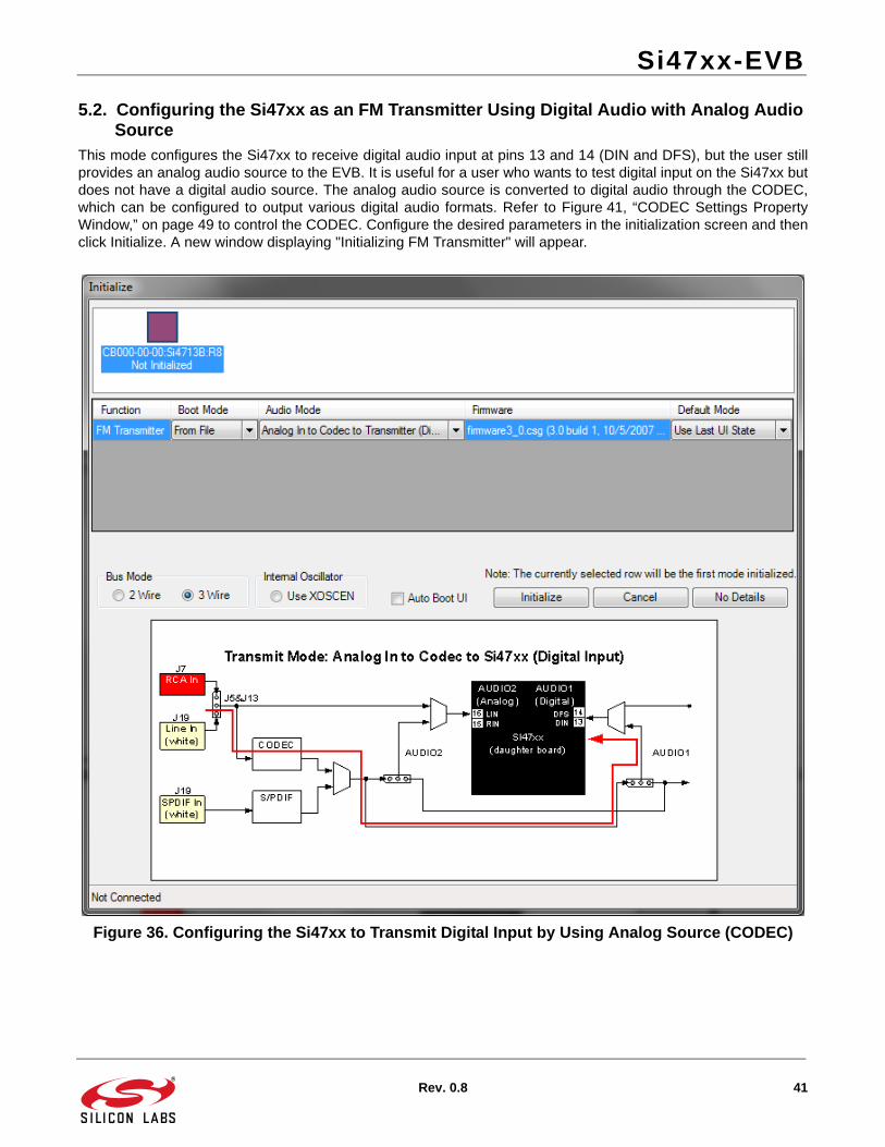
The first Si47xx window is the Initialization window as shown in Figure 35.
Select the FM transmitter function.
As an FM transmitter, there are three audio input settings available:
Analog Input
Analog to Digital Input
Digital Input
5.1. Configuring the Si47xx as an FM Transmitter Using Analog Audio InputThis mode configures the Si47xx to receive analog audio input at pins 15 and 16 (LIN and RIN). The user has theability to provide analog audio from RCA In connector (J7) or Line In (J19). Set jumpers J5 and J13 accordingly.
Figure 35 shows the configuration setting for analog audio input. Configure the desired parameters in theinitialization screen and then click Initialize. A new window displaying "Initializing FM Transmitter" will appear.
Figure 35. Configuring the Si47xx to Transmit Analog Input
Si47xx-EVB
Rev. 0.8 41
5.2. Configuring the Si47xx as an FM Transmitter Using Digital Audio with Analog Audio Source
This mode configures the Si47xx to receive digital audio input at pins 13 and 14 (DIN and DFS), but the user stillprovides an analog audio source to the EVB. It is useful for a user who wants to test digital input on the Si47xx butdoes not have a digital audio source. The analog audio source is converted to digital audio through the CODEC,which can be configured to output various digital audio formats. Refer to Figure 41, “CODEC Settings PropertyWindow,” on page 49 to control the CODEC. Configure the desired parameters in the initialization screen and thenclick Initialize. A new window displaying "Initializing FM Transmitter" will appear.
Figure 36. Configuring the Si47xx to Transmit Digital Input by Using Analog Source (CODEC)
Si47xx-EVB
42 Rev. 0.8
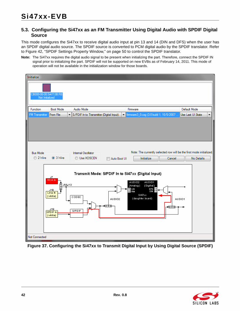
5.3. Configuring the Si47xx as an FM Transmitter Using Digital Audio with SPDIF Digital Source
This mode configures the Si47xx to receive digital audio input at pin 13 and 14 (DIN and DFS) when the user hasan SPDIF digital audio source. The SPDIF source is converted to PCM digital audio by the SPDIF translator. Referto Figure 42, “SPDIF Settings Property Window,” on page 50 to control the SPDIF translator.
Note: The Si47xx requires the digital audio signal to be present when initializing the part. Therefore, connect the SPDIF IN signal prior to initializing the part. SPDIF will not be supported on new EVBs as of February 14, 2011. This mode of operation will not be available in the initialization window for those boards.
Figure 37. Configuring the Si47xx to Transmit Digital Input by Using Digital Source (SPDIF)
Si47xx-EVB
Rev. 0.8 43
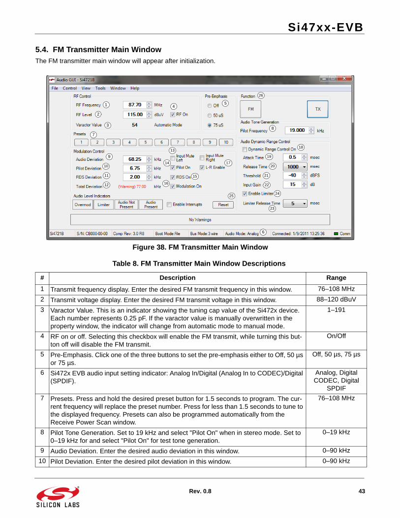
5.4. FM Transmitter Main WindowThe FM transmitter main window will appear after initialization.
Figure 38. FM Transmitter Main Window
Table 8. FM Transmitter Main Window Descriptions
# Description Range
1 Transmit frequency display. Enter the desired FM transmit frequency in this window. 76–108 MHz
2 Transmit voltage display. Enter the desired FM transmit voltage in this window. 88–120 dBuV
3 Varactor Value. This is an indicator showing the tuning cap value of the Si472x device. Each number represents 0.25 pF. If the varactor value is manually overwritten in the property window, the indicator will change from automatic mode to manual mode.
1–191
4 RF on or off. Selecting this checkbox will enable the FM transmit, while turning this but-ton off will disable the FM transmit.
On/Off
5 Pre-Emphasis. Click one of the three buttons to set the pre-emphasis either to Off, 50 µs or 75 µs.
Off, 50 µs, 75 µs
6 Si472x EVB audio input setting indicator: Analog In/Digital (Analog In to CODEC)/Digital (SPDIF).
Analog, Digital CODEC, Digital
SPDIF
7 Presets. Press and hold the desired preset button for 1.5 seconds to program. The cur-rent frequency will replace the preset number. Press for less than 1.5 seconds to tune to the displayed frequency. Presets can also be programmed automatically from the Receive Power Scan window.
76–108 MHz
8 Pilot Tone Generation. Set to 19 kHz and select "Pilot On" when in stereo mode. Set to 0–19 kHz for and select "Pilot On" for test tone generation.
0–19 kHz
9 Audio Deviation. Enter the desired audio deviation in this window. 0–90 kHz
10 Pilot Deviation. Enter the desired pilot deviation in this window. 0–90 kHz
1
2
3
45
6
7
8
9
11
10
12
13
14
15
16
17
18
19
20
21
22
23
2425
26
Si47xx-EVB
44 Rev. 0.8
11 RDS Deviation. Enter the desired RDS deviation in this window (Si4711/13/21 only). 0–7.5 kHz
12 Total Deviation. This is an indicator only displaying the sum of the audio, pilot and RDS deviation. If the total deviation exceeds 75 kHz, the indicator will turn red and a warning sign is displayed.
0–187.5 kHz
13 Input Mute Left/Right. Selecting this checkbox will mute the Left or Right audio channel. On/Off
14 Turn on or off the pilot tone for stereo or mono FM transmit mode. On/Off
15 Turn on or off the RDS transmission (Si4711/13/21 only). On/Off
16 Modulation On. Selecting this checkbox will modulate the audio, pilot, and RDS signal according to the audio, pilot, and RDS deviation. De-selecting this checkbox will turn off modulation for all audio, pilot, and RDS signal and only the carrier will be transmitted.
On/Off
17 Turn on or off the L-R channel for stereo or mono FM transmit mode. On/Off
18 Turn on or off the compressor for the audio signal. On/Off
19 Attack time. Set the attack time for the compressor in milliseconds. 0.5–5 ms
20 Release time. Set the release time for the compressor in milliseconds. 100–1000 ms
21 Threshold. Set the threshold for the compressor. –40 to 0 dBFS
22 Input Gain. Set the compressor gain. 0 to 20 dB
23 Limiter Release Time. Set the limiter release time constant.(Not available in Si4710-A10).
0.5,1,2,3,4,5,6,7,8,9,10,20,30,40,50,
75,100 ms
24 Turn on or off the limiter feature. On/Off
25 Audio Level Indicators. Overmodulation, Limiter, Audio input level below low-level threshold (silence detection), and Audio input level below high-level threshold (loud detection). To enable these four indicators, check the Enable Interrupts box. These indicators are sticky; to clear them, click the Reset button.
26 Mode switch buttons to switch between different modes on the device. See section 4 for more information.
Table 8. FM Transmitter Main Window Descriptions (Continued)
# Description Range
Si47xx-EVB
Rev. 0.8 45
5.5. FM Transmitter Settings (Analog Mode) Property WindowFM transmitter settings can be configured through the properties window by selecting WindowProperties.Properties are grouped into categories which can be selected from the drop-down box in the upper right of thewindow. For convenience, all FM transmitter properties are also located in WindowPropertiesTX: All. Analogmode properties will be available if Analog Mode was selected in the initialization window.
Figure 39. FM Transmitter Settings in Analog Mode Property Window
Table 9. FM Transmitter Settings in Analog Mode Property Window Descriptions
Item Description Range Devices
Line Input Attenuation (k)
The Si47xx has four attenuator settings (636, 416, 301, and 190 mVp). It will tell the maximum audio input signal that the user can give to the LIN and RIN input. The attenuator setting will determine the audio input impedance (LIN and RIN) of the device.
190 mVp, 301 mVpk, 416 mVp, 636 mVpk
All
Maximum Line Input Level (mVpk)
The maximum line input level of the max audio input signal that the user supplies to the device. This num-ber has to be less than or equal to the attenuation set-ting. The max line input level will correspond to the max audio deviation set in the audio deviation window on the main GUI. Make sure that the actual audio input signal does not exceed this limit, otherwise the audio signal will become distorted.
0–Line Input Attenu-ation
All
Reference Clock Frequency (Hz)
This field is used to specify the frequency of the reference clock. The input to the RCLK pin divided by the prescaler is the reference clock. The reference clock must be in the range of 31130 to 34406 Hz.
31130–34406 Hz All
Si47xx-EVB
46 Rev. 0.8
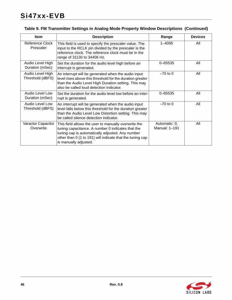
Reference Clock Prescaler
This field is used to specify the prescaler value. The input to the RCLK pin divided by the prescaler is the reference clock. The reference clock must be in the range of 31130 to 34406 Hz.
1–4095 All
Audio Level High Duration (mSec)
Set the duration for the audio level high before an interrupt is generated.
0–65535 All
Audio Level High Threshold (dBFS)
An interrupt will be generated when the audio input level rises above this threshold for the duration greater than the Audio Level High Duration setting. This may also be called loud detection indicator.
–70 to 0 All
Audio Level Low Duration (mSec)
Set the duration for the audio level low before an inter-rupt is generated.
0–65535 All
Audio Level Low Threshold (dBFS)
An interrupt will be generated when the audio input level falls below this threshold for the duration greater than the Audio Level Low Distortion setting. This may be called silence detection indicator.
–70 to 0 All
Varactor Capacitor Overwrite
This field allows the user to manually overwrite the tuning capacitance. A number 0 indicates that the tuning cap is automatically adjusted. Any number other than 0 (1 to 191) will indicate that the tuning cap is manually adjusted.
Automatic: 0, Manual: 1–191
All
Table 9. FM Transmitter Settings in Analog Mode Property Window Descriptions (Continued)
Item Description Range Devices
Si47xx-EVB
Rev. 0.8 47
5.6. FM Transmitter Settings (Digital Mode) Property WindowFM transmitter settings can be configured through the properties window by selecting WindowProperties.Properties are grouped into categories which can be selected from the drop-down box in the upper right of thewindow. For convenience, all FM transmitter properties are also located in WindowProperties TX: All. Digitalmode properties will be available if CODED or SPDIF modes was selected in the initialization window.
Figure 40. FM Transmitter Settings in Digital Mode Property Window
Table 10. FM Transmitter Settings in Digital Mode Property Window Descriptions
Item Description Range Applicable Devices
Reference Clock Frequency (Hz)
This field is used to specify the frequency of the refer-ence clock. The input to the RCLK pin divided by the prescaler is the reference clock. The reference clock must be in the range of 31130 to 34406 Hz.
31130–34406 Hz All
Reference Clock Prescaler
This field is used to specify the prescaler value. The input to the RCLK pin divided by the prescaler is the reference clock. The reference clock must be in the range of 31130 to 34406 Hz.
1–4095 All
Digital Format Sets I2S of left justified digital format. Left-Justified, I2S, DSP (MSB on first
DCLK), or DSP (MSB on second
DCLK)
All except Si4710-A10
Digital Sample Precision
Select the precision of the digital audio input. 8, 16, 20, 24 bits All
Digital Sample Rate (Hz)
Sets the DFS digital sample rate. Must be set to 0 Hz before DCLK/DFS is removed.
0, 32000–48000 Hz
All except Si4710-A10
Si47xx-EVB
48 Rev. 0.8
Digital Mono Mode Enable
Select between Digital Stereo or Mono. On/Off All
Digital DCLK Falling Edge
Select between using rising edge or falling edge of DCLK when sampling Digital Input (DIN) data.
On/Off All
Audio Level Low Threshold (dBFS)
An interrupt will be generated when the audio input level falls below this threshold for the duration greater than the Audio Level Low Distortion setting. This may be called silence detection indicator.
–70 to 0 All
Audio Level Low Duration (mSec)
Set the duration for the audio level low before an interrupt is generated.
0–65535 All
Audio Level High Threshold (dBFS)
An interrupt will be generated when the audio input level rises above this threshold for the duration greater than the Audio Level High Duration setting. This may also be called loud detection indicator.
–70 to 0 All
Audio Level High Duration (mSec)
Set the duration for the audio level high before an interrupt is generated.
0–65535 All
Varactor Capacitor Overwrite
This field allows the user to manually overwrite the tuning capacitance. 0 indicates that the tuning cap is automatically adjusted. Any number other than 0 (1 to 191) will indicate that the tuning cap is manually adjusted.
Automatic: 0 Manual: 1–191
All
Table 10. FM Transmitter Settings in Digital Mode Property Window Descriptions (Continued)
Item Description Range Applicable Devices
Si47xx-EVB
Rev. 0.8 49
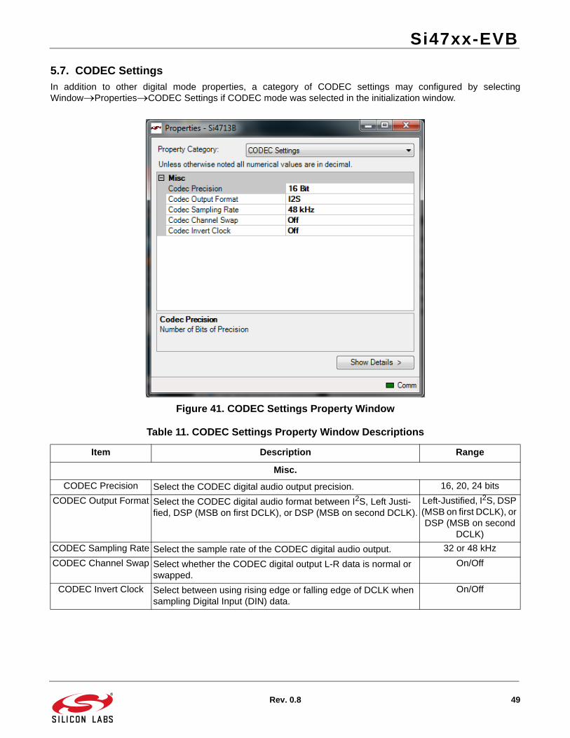
5.7. CODEC SettingsIn addition to other digital mode properties, a category of CODEC settings may configured by selectingWindowPropertiesCODEC Settings if CODEC mode was selected in the initialization window.
Figure 41. CODEC Settings Property Window
Table 11. CODEC Settings Property Window Descriptions
Item Description Range
Misc.
CODEC Precision Select the CODEC digital audio output precision. 16, 20, 24 bits
CODEC Output Format Select the CODEC digital audio format between I2S, Left Justi-fied, DSP (MSB on first DCLK), or DSP (MSB on second DCLK).
Left-Justified, I2S, DSP (MSB on first DCLK), or DSP (MSB on second
DCLK)
CODEC Sampling Rate Select the sample rate of the CODEC digital audio output. 32 or 48 kHz
CODEC Channel Swap Select whether the CODEC digital output L-R data is normal or swapped.
On/Off
CODEC Invert Clock Select between using rising edge or falling edge of DCLK when sampling Digital Input (DIN) data.
On/Off
Si47xx-EVB
50 Rev. 0.8
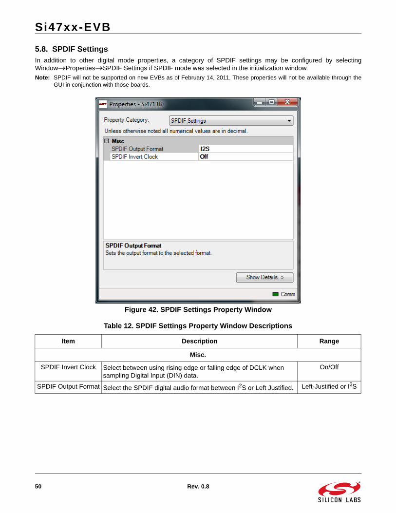
5.8. SPDIF SettingsIn addition to other digital mode properties, a category of SPDIF settings may be configured by selectingWindowPropertiesSPDIF Settings if SPDIF mode was selected in the initialization window.
Note: SPDIF will not be supported on new EVBs as of February 14, 2011. These properties will not be available through theGUI in conjunction with those boards.
Figure 42. SPDIF Settings Property Window
Table 12. SPDIF Settings Property Window Descriptions
Item Description Range
Misc.
SPDIF Invert Clock Select between using rising edge or falling edge of DCLK when sampling Digital Input (DIN) data.
On/Off
SPDIF Output Format Select the SPDIF digital audio format between I2S or Left Justified. Left-Justified or I2S
Si47xx-EVB
Rev. 0.8 51
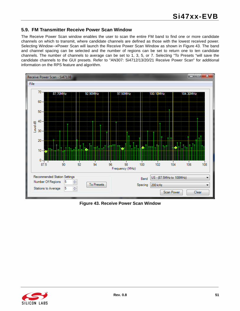
5.9. FM Transmitter Receive Power Scan WindowThe Receive Power Scan window enables the user to scan the entire FM band to find one or more candidatechannels on which to transmit, where candidate channels are defined as those with the lowest received power.Selecting WindowPower Scan will launch the Receive Power Scan Window as shown in Figure 43. The bandand channel spacing can be selected and the number of regions can be set to return one to ten candidatechannels. The number of channels to average can be set to 1, 3, 5, or 7. Selecting “To Presets “will save thecandidate channels to the GUI presets. Refer to "AN307: Si4712/13/20/21 Receive Power Scan" for additionalinformation on the RPS feature and algorithm.
Figure 43. Receive Power Scan Window
Si47xx-EVB
52 Rev. 0.8
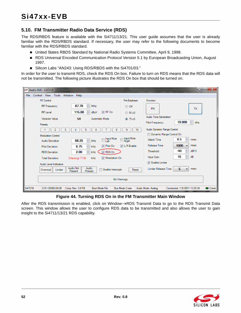
5.10. FM Transmitter Radio Data Service (RDS)The RDS/RBDS feature is available with the Si4711/13/21. This user guide assumes that the user is alreadyfamiliar with the RDS/RBDS standard. If necessary, the user may refer to the following documents to becomefamiliar with the RDS/RBDS standard.
United States RBDS Standard by National Radio Systems Committee, April 9, 1998.
RDS Universal Encoded Communication Protocol Version 5.1 by European Broadcasting Union, August 1997.
Silicon Labs “AN243: Using RDS/RBDS with the Si4701/03.”
In order for the user to transmit RDS, check the RDS On box. Failure to turn on RDS means that the RDS data willnot be transmitted. The following picture illustrates the RDS On box that should be turned on.
Figure 44. Turning RDS On in the FM Transmitter Main Window
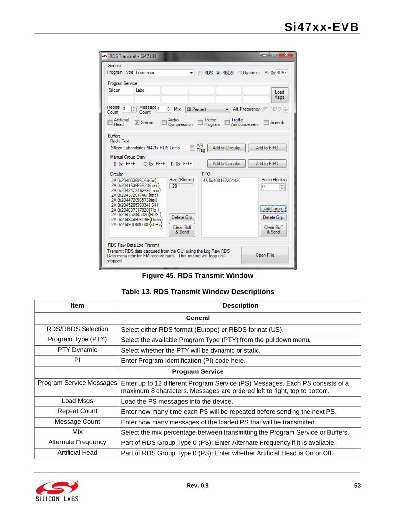
After the RDS transmission is enabled, click on WindowRDS Transmit Data to go to the RDS Transmit Datascreen. This window allows the user to configure RDS data to be transmitted and also allows the user to gaininsight to the Si4711/13/21 RDS capability.
Si47xx-EVB
Rev. 0.8 53
Figure 45. RDS Transmit Window
Table 13. RDS Transmit Window Descriptions
Item Description
General
RDS/RBDS Selection Select either RDS format (Europe) or RBDS format (US).
Program Type (PTY) Select the available Program Type (PTY) from the pulldown menu.
PTY Dynamic Select whether the PTY will be dynamic or static.
PI Enter Program Identification (PI) code here.
Program Service
Program Service Messages Enter up to 12 different Program Service (PS) Messages. Each PS consists of a maximum 8 characters. Messages are ordered left to right, top to bottom.
Load Msgs Load the PS messages into the device.
Repeat Count Enter how many time each PS will be repeated before sending the next PS.
Message Count Enter how many messages of the loaded PS that will be transmitted.
Mix Select the mix percentage between transmitting the Program Service or Buffers.
Alternate Frequency Part of RDS Group Type 0 (PS): Enter Alternate Frequency if it is available.
Artificial Head Part of RDS Group Type 0 (PS): Enter whether Artificial Head is On or Off.
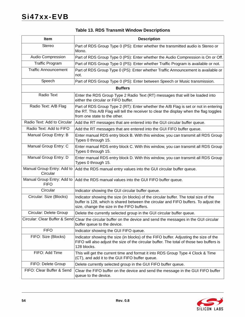
Si47xx-EVB
54 Rev. 0.8
Stereo Part of RDS Group Type 0 (PS): Enter whether the transmitted audio is Stereo or Mono.
Audio Compression Part of RDS Group Type 0 (PS): Enter whether the Audio Compression is On or Off.
Traffic Program Part of RDS Group Type 0 (PS): Enter whether Traffic Program is available or not.
Traffic Announcement Part of RDS Group Type 0 (PS): Enter whether Traffic Announcement is available or not.
Speech Part of RDS Group Type 0 (PS): Enter between Speech or Music transmission.
Buffers
Radio Text Enter the RDS Group Type 2 Radio Text (RT) messages that will be loaded into either the circular or FIFO buffer.
Radio Text: A/B Flag Part of RDS Group Type 2 (RT): Enter whether the A/B Flag is set or not in entering the RT. This A/B Flag will tell the receiver to clear the display when the flag toggles from one state to the other.
Radio Text: Add to Circular Add the RT messages that are entered into the GUI circular buffer queue.
Radio Text: Add to FIFO Add the RT messages that are entered into the GUI FIFO buffer queue.
Manual Group Entry: B Enter manual RDS entry block B. With this window, you can transmit all RDS Group Types 0 through 15.
Manual Group Entry: C Enter manual RDS entry block C. With this window, you can transmit all RDS Group Types 0 through 15.
Manual Group Entry: D Enter manual RDS entry block D. With this window, you can transmit all RDS Group Types 0 through 15.
Manual Group Entry: Add to Circular
Add the RDS manual entry values into the GUI circular buffer queue.
Manual Group Entry: Add to FIFO
Add the RDS manual values into the GUI FIFO buffer queue.
Circular Indicator showing the GUI circular buffer queue.
Circular: Size (Blocks) Indicator showing the size (in blocks) of the circular buffer. The total size of the buffer is 128, which is shared between the circular and FIFO buffers. To adjust the size, change the size in the FIFO buffers.
Circular: Delete Group Delete the currently selected group in the GUI circular buffer queue.
Circular: Clear Buffer & Send Clear the circular buffer on the device and send the messages in the GUI circular buffer queue to the device.
FIFO Indicator showing the GUI FIFO queue.
FIFO: Size (Blocks) Indicator showing the size (in blocks) of the FIFO buffer. Adjusting the size of the FIFO will also adjust the size of the circular buffer. The total of those two buffers is 128 blocks.
FIFO: Add Time This will get the current time and format it into RDS Group Type 4 Clock & Time (CT), and add it to the GUI FIFO buffer queue.
FIFO: Delete Group Delete currently selected group in the GUI FIFO buffer queue.
FIFO: Clear Buffer & Send Clear the FIFO buffer on the device and send the message in the GUI FIFO buffer queue to the device.
Table 13. RDS Transmit Window Descriptions
Item Description
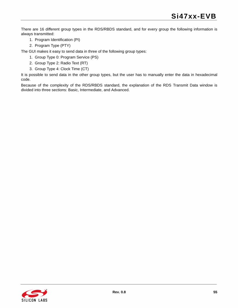
Si47xx-EVB
Rev. 0.8 55
There are 16 different group types in the RDS/RBDS standard, and for every group the following information isalways transmitted:
1. Program Identification (PI)
2. Program Type (PTY)
The GUI makes it easy to send data in three of the following group types:
1. Group Type 0: Program Service (PS)
2. Group Type 2: Radio Text (RT)
3. Group Type 4: Clock Time (CT)
It is possible to send data in the other group types, but the user has to manually enter the data in hexadecimalcode.
Because of the complexity of the RDS/RBDS standard, the explanation of the RDS Transmit Data window isdivided into three sections: Basic, Intermediate, and Advanced.
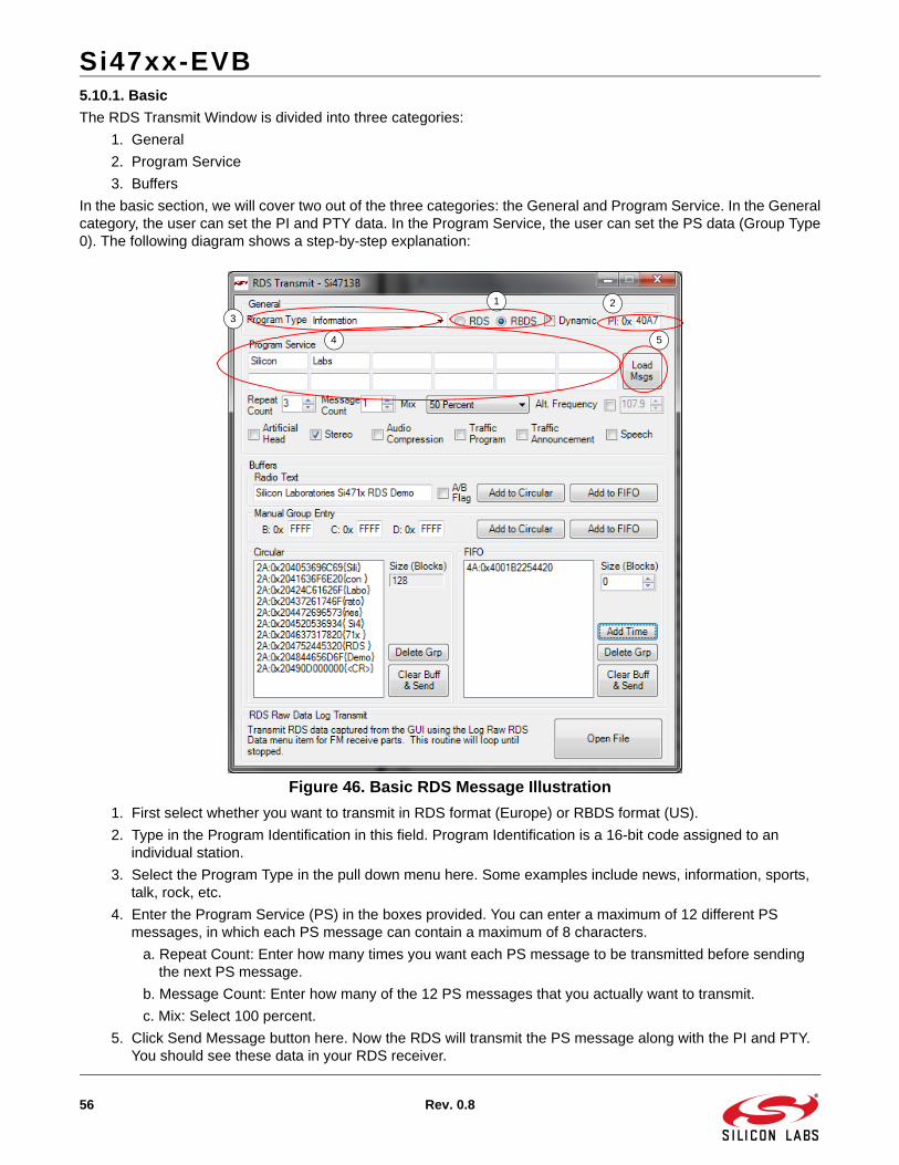
Si47xx-EVB
56 Rev. 0.8
5.10.1. Basic
The RDS Transmit Window is divided into three categories:
1. General
2. Program Service
3. Buffers
In the basic section, we will cover two out of the three categories: the General and Program Service. In the Generalcategory, the user can set the PI and PTY data. In the Program Service, the user can set the PS data (Group Type0). The following diagram shows a step-by-step explanation:
Figure 46. Basic RDS Message Illustration
1. First select whether you want to transmit in RDS format (Europe) or RBDS format (US).
2. Type in the Program Identification in this field. Program Identification is a 16-bit code assigned to an individual station.
3. Select the Program Type in the pull down menu here. Some examples include news, information, sports, talk, rock, etc.
4. Enter the Program Service (PS) in the boxes provided. You can enter a maximum of 12 different PS messages, in which each PS message can contain a maximum of 8 characters.
a. Repeat Count: Enter how many times you want each PS message to be transmitted before sending the next PS message.
b. Message Count: Enter how many of the 12 PS messages that you actually want to transmit.
c. Mix: Select 100 percent.
5. Click Send Message button here. Now the RDS will transmit the PS message along with the PI and PTY. You should see these data in your RDS receiver.
2
3
4
1
5
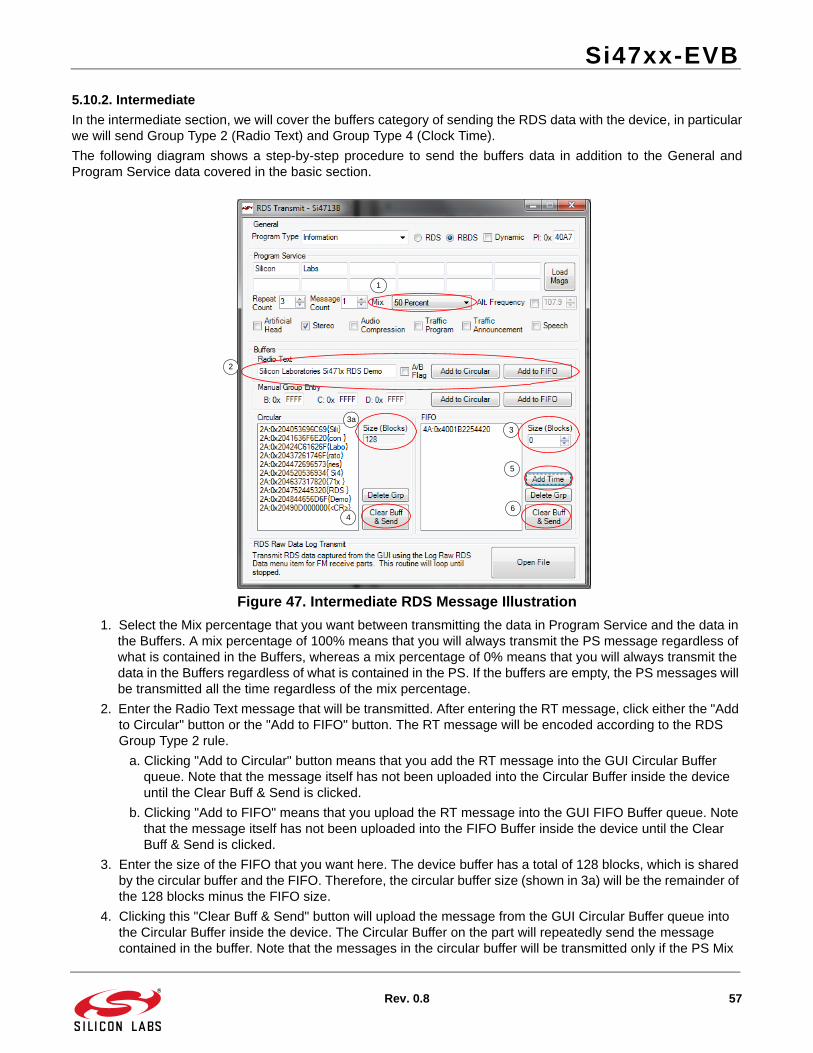
Si47xx-EVB
Rev. 0.8 57
5.10.2. Intermediate
In the intermediate section, we will cover the buffers category of sending the RDS data with the device, in particularwe will send Group Type 2 (Radio Text) and Group Type 4 (Clock Time).
The following diagram shows a step-by-step procedure to send the buffers data in addition to the General andProgram Service data covered in the basic section.
Figure 47. Intermediate RDS Message Illustration
1. Select the Mix percentage that you want between transmitting the data in Program Service and the data in the Buffers. A mix percentage of 100% means that you will always transmit the PS message regardless of what is contained in the Buffers, whereas a mix percentage of 0% means that you will always transmit the data in the Buffers regardless of what is contained in the PS. If the buffers are empty, the PS messages will be transmitted all the time regardless of the mix percentage.
2. Enter the Radio Text message that will be transmitted. After entering the RT message, click either the "Add to Circular" button or the "Add to FIFO" button. The RT message will be encoded according to the RDS Group Type 2 rule.
a. Clicking "Add to Circular" button means that you add the RT message into the GUI Circular Buffer queue. Note that the message itself has not been uploaded into the Circular Buffer inside the device until the Clear Buff & Send is clicked.
b. Clicking "Add to FIFO" means that you upload the RT message into the GUI FIFO Buffer queue. Note that the message itself has not been uploaded into the FIFO Buffer inside the device until the Clear Buff & Send is clicked.
3. Enter the size of the FIFO that you want here. The device buffer has a total of 128 blocks, which is shared by the circular buffer and the FIFO. Therefore, the circular buffer size (shown in 3a) will be the remainder of the 128 blocks minus the FIFO size.
4. Clicking this "Clear Buff & Send" button will upload the message from the GUI Circular Buffer queue into the Circular Buffer inside the device. The Circular Buffer on the part will repeatedly send the message contained in the buffer. Note that the messages in the circular buffer will be transmitted only if the PS Mix
2
3
4
1
5
3a
6
Si47xx-EVB
58 Rev. 0.8
value is set to anything other than 100%.
5. Clicking the "Add Time" button here will add the current time as a RDS Group Type 4 message to the GUI FIFO Buffer queue.
6. Clicking the "Clear Buff & Send" button will upload the message from the FIFO Buffer Indicator Window into the FIFO Buffer inside the device. The FIFO Buffer on the part will only send the messages contained in the buffer once. A good example of using FIFO buffer is when you want to send the time data. Time is something that occurs only once, so it will not be beneficial to upload time to the circular buffer and transmit it continuously. Refer to step 5 for information on sending time data. Note that the messages in the FIFO buffer will be transmitted only if the PS Mix value is set to anything other than 100%.
5.10.3. Advanced
In the advanced section, we will cover the remaining RDS topics.
Figure 48. Advanced RDS Sending Illustration
1. Dynamic: This tells whether the PTY code is static or dynamic.
2. Alternate Frequency: This provides the ability to inform the receiver of a single alternate frequency. This field is transmitted along with the Group Type 0 (PS).
3. Miscellaneous bits in Group Type 0 (PS):
a. Artificial Head: 0 = Not Artificial Head; 1 = Artificial Head
b. Stereo: 0 = Mono; 1 = Stereo
c. Audio Compressor: 0 = Not compressed; 1 = Compressed
d. Traffic Program (TP): 0 = No TP; 1 = TP
e. Traffic Announcement (TA): 0 = No TA; 1 = TA
f. Speech: 0 = Speech; 1= Music
4. A/B Flag: This is an important flag in the RDS Group Type 2 (RT). Checking this box when a Radio Text is
2
3
4
1
5
6
7
8
9

Si47xx-EVB
Rev. 0.8 59
uploaded means that the RT is uploaded with the flag set. Un-checking this box when an RT is uploaded means that the flag is not set. This flag tells the receiver that when the flag toggles from set to reset or vice versa, the receiver will clear the display before showing the next RT.
5. Manual Group Entry: Use this box to upload the RDS data manually. You can use this box to upload messages from the Group Type for which the GUI does not have encoding support. For these messages, the user must encode the messages into hexadecimal code.
6. Circular Buffer Indicator: This displays the message that gets uploaded into the Circular Buffer in hexadecimal code. This can be useful to see how the Group Type 0 (PS), Type 2 (RT), and Type 4 (CT) is encoded into RDS data.
7. Delete Circular Buffer Group: This deletes a group that is selected in the Circular Buffer Indicator.
8. FIFO Buffer Indicator: This displays the message that gets uploaded into the FIFO buffer in hexadecimal code.
9. Delete FIFO Buffer Group: This deletes a group that is selected in the FIFO Buffer Indicator.
Si47xx-EVB
60 Rev. 0.8
5.11. FM Transmitter Register Map WindowThe register map window allows the user to manually program the device by sending commands to the chip. Referto “AN332: Si47xx Programming Guide” to manually program the device. Clicking on WindowRegister Map willlaunch the Register Map Window as shown in Figure 49.
Figure 49. FM Transmitter Register Map Window
Si47xx-EVB
Rev. 0.8 61
6. FM Receiver GUI
The first Si47xx window is the Initialization window as shown in Figure 50.
Select the FM receiver function.
As an FM receiver, analog audio out is available on pins 13 and 14.
6.1. Configuring the Si47xx as an FM ReceiverSelect the device, busmode, firmware revision, and initial part settings and then click Initialize. A new windowdisplaying "Initializing FM Receiver" will appear. If you check “Use XOSCEN,” the daughtercard crystal and on-chiposcillator will be used to clock the Si47xx. Crystal operation is not supported on Si474x-EVB (that supports Si4740/41/42/43/44/45) and Si4749-EVB. You can use the EVB Audio Settings drop down box to select the audio modeused by the Si47xx part. See Section 2.1.4 of the Si47xx-EVB User’s Guide for more information on this setting.The Si4749 can also be programmed as an RDS only tuner. This selection is available through the EVB AudioSetting drop down box as well.
Note: As of February 2011, SPDIF is not supported on new EVBs. Modes of operation requiring the SPDIF will not be availablein the initialization window for those boards.
Figure 50. FM Receiver Initialization
Si47xx-EVB
62 Rev. 0.8
6.2. FM Receiver Main WindowThe FM receiver main window will appear after initialization.
Figure 51. FM Receiver Main Window
Figure 52. FM Receiver Main Window for Si474x
1 2 3
45
6
1
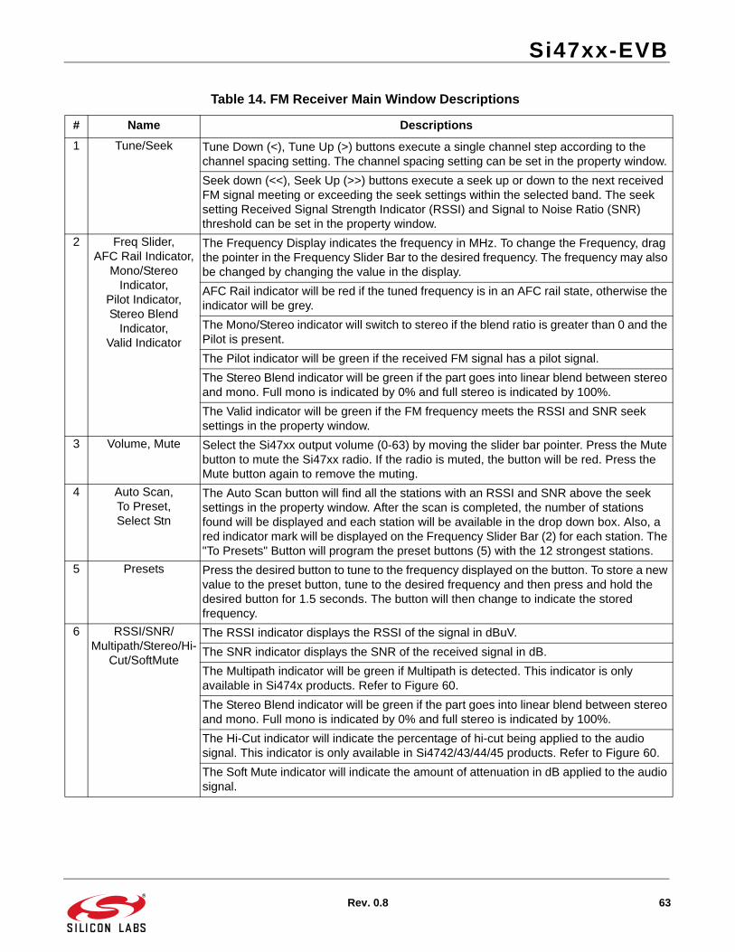
Si47xx-EVB
Rev. 0.8 63
Table 14. FM Receiver Main Window Descriptions
# Name Descriptions
1 Tune/Seek Tune Down (<), Tune Up (>) buttons execute a single channel step according to the channel spacing setting. The channel spacing setting can be set in the property window.
Seek down (<<), Seek Up (>>) buttons execute a seek up or down to the next received FM signal meeting or exceeding the seek settings within the selected band. The seek setting Received Signal Strength Indicator (RSSI) and Signal to Noise Ratio (SNR) threshold can be set in the property window.
2 Freq Slider, AFC Rail Indicator,
Mono/Stereo Indicator,
Pilot Indicator, Stereo Blend
Indicator, Valid Indicator
The Frequency Display indicates the frequency in MHz. To change the Frequency, drag the pointer in the Frequency Slider Bar to the desired frequency. The frequency may also be changed by changing the value in the display.
AFC Rail indicator will be red if the tuned frequency is in an AFC rail state, otherwise the indicator will be grey.
The Mono/Stereo indicator will switch to stereo if the blend ratio is greater than 0 and the Pilot is present.
The Pilot indicator will be green if the received FM signal has a pilot signal.
The Stereo Blend indicator will be green if the part goes into linear blend between stereo and mono. Full mono is indicated by 0% and full stereo is indicated by 100%.
The Valid indicator will be green if the FM frequency meets the RSSI and SNR seek settings in the property window.
3 Volume, Mute Select the Si47xx output volume (0-63) by moving the slider bar pointer. Press the Mute button to mute the Si47xx radio. If the radio is muted, the button will be red. Press the Mute button again to remove the muting.
4 Auto Scan, To Preset, Select Stn
The Auto Scan button will find all the stations with an RSSI and SNR above the seek settings in the property window. After the scan is completed, the number of stations found will be displayed and each station will be available in the drop down box. Also, a red indicator mark will be displayed on the Frequency Slider Bar (2) for each station. The "To Presets" Button will program the preset buttons (5) with the 12 strongest stations.
5 Presets Press the desired button to tune to the frequency displayed on the button. To store a new value to the preset button, tune to the desired frequency and then press and hold the desired button for 1.5 seconds. The button will then change to indicate the stored frequency.
6 RSSI/SNR/Multipath/Stereo/Hi-
Cut/SoftMute
The RSSI indicator displays the RSSI of the signal in dBuV.
The SNR indicator displays the SNR of the received signal in dB.
The Multipath indicator will be green if Multipath is detected. This indicator is only available in Si474x products. Refer to Figure 60.
The Stereo Blend indicator will be green if the part goes into linear blend between stereo and mono. Full mono is indicated by 0% and full stereo is indicated by 100%.
The Hi-Cut indicator will indicate the percentage of hi-cut being applied to the audio signal. This indicator is only available in Si4742/43/44/45 products. Refer to Figure 60.
The Soft Mute indicator will indicate the amount of attenuation in dB applied to the audio signal.
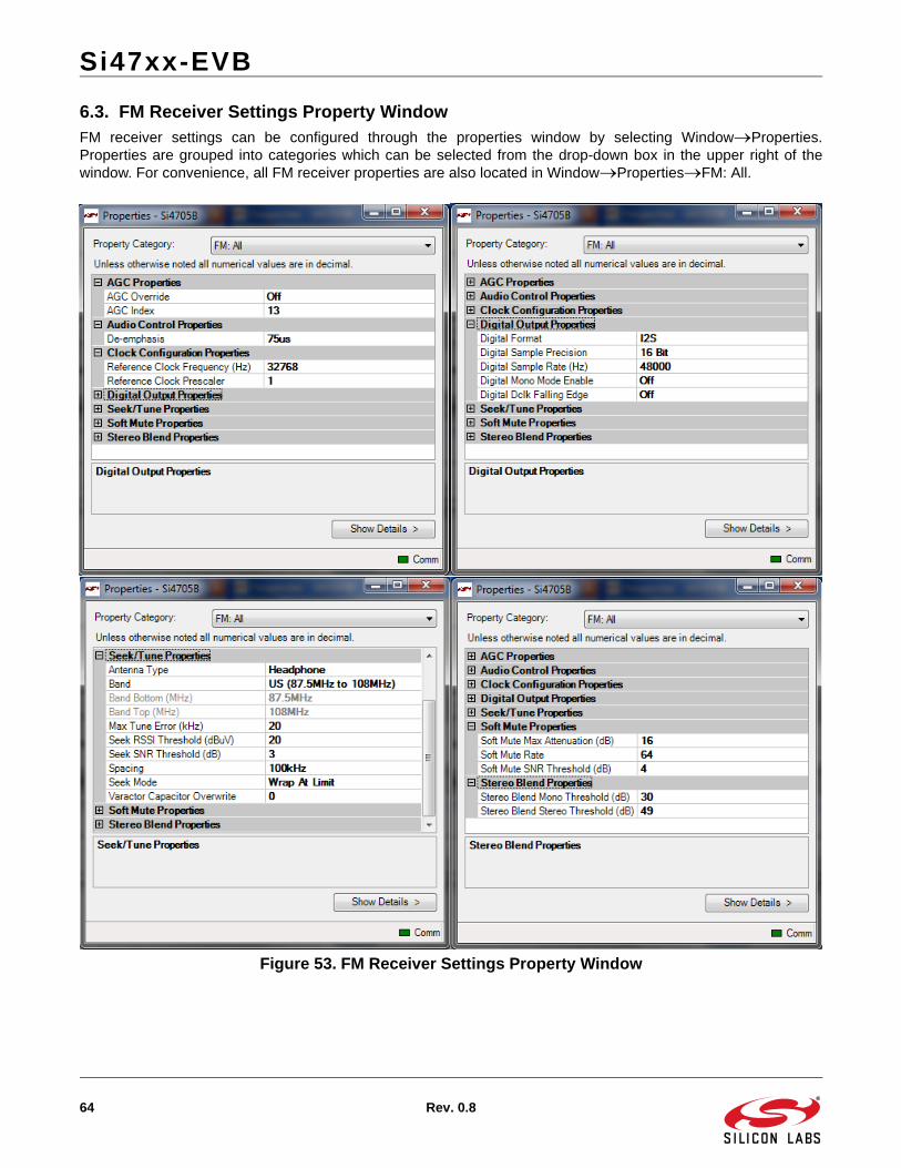
Si47xx-EVB
64 Rev. 0.8
6.3. FM Receiver Settings Property WindowFM receiver settings can be configured through the properties window by selecting WindowProperties.Properties are grouped into categories which can be selected from the drop-down box in the upper right of thewindow. For convenience, all FM receiver properties are also located in WindowPropertiesFM: All.
Figure 53. FM Receiver Settings Property Window
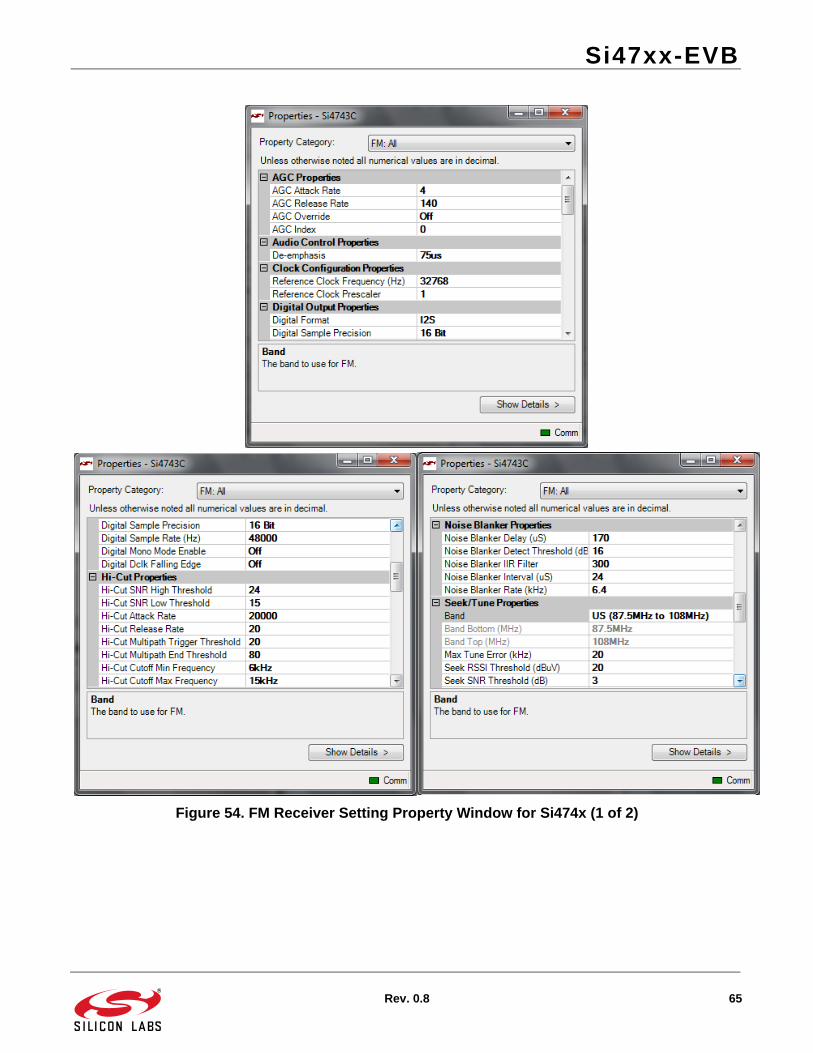
Si47xx-EVB
Rev. 0.8 65
Figure 54. FM Receiver Setting Property Window for Si474x (1 of 2)

Si47xx-EVB
66 Rev. 0.8
Figure 55. FM Receiver Setting Property Window for Si474x continued (2 of 2)
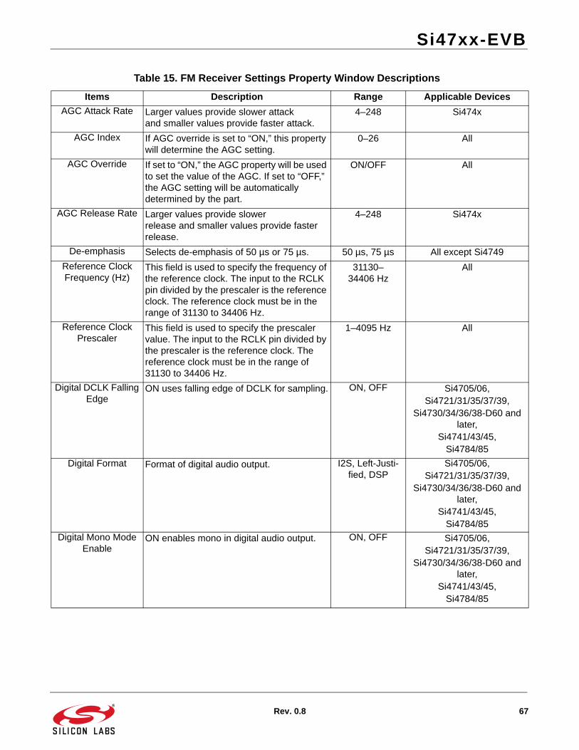
Si47xx-EVB
Rev. 0.8 67
Table 15. FM Receiver Settings Property Window Descriptions
Items Description Range Applicable Devices
AGC Attack Rate Larger values provide slower attackand smaller values provide faster attack.
4–248 Si474x
AGC Index If AGC override is set to “ON,” this property will determine the AGC setting.
0–26 All
AGC Override If set to “ON,” the AGC property will be used to set the value of the AGC. If set to “OFF,” the AGC setting will be automatically determined by the part.
ON/OFF All
AGC Release Rate Larger values provide slowerrelease and smaller values provide faster release.
4–248 Si474x
De-emphasis Selects de-emphasis of 50 µs or 75 µs. 50 µs, 75 µs All except Si4749
Reference Clock Frequency (Hz)
This field is used to specify the frequency of the reference clock. The input to the RCLK pin divided by the prescaler is the reference clock. The reference clock must be in the range of 31130 to 34406 Hz.
31130–34406 Hz
All
Reference Clock Prescaler
This field is used to specify the prescaler value. The input to the RCLK pin divided by the prescaler is the reference clock. The reference clock must be in the range of 31130 to 34406 Hz.
1–4095 Hz All
Digital DCLK Falling Edge
ON uses falling edge of DCLK for sampling. ON, OFF Si4705/06,Si4721/31/35/37/39,
Si4730/34/36/38-D60 and later,
Si4741/43/45,Si4784/85
Digital Format Format of digital audio output. I2S, Left-Justi-fied, DSP
Si4705/06,Si4721/31/35/37/39,
Si4730/34/36/38-D60 and later,
Si4741/43/45,Si4784/85
Digital Mono Mode Enable
ON enables mono in digital audio output. ON, OFF Si4705/06,Si4721/31/35/37/39,
Si4730/34/36/38-D60 and later,
Si4741/43/45,Si4784/85
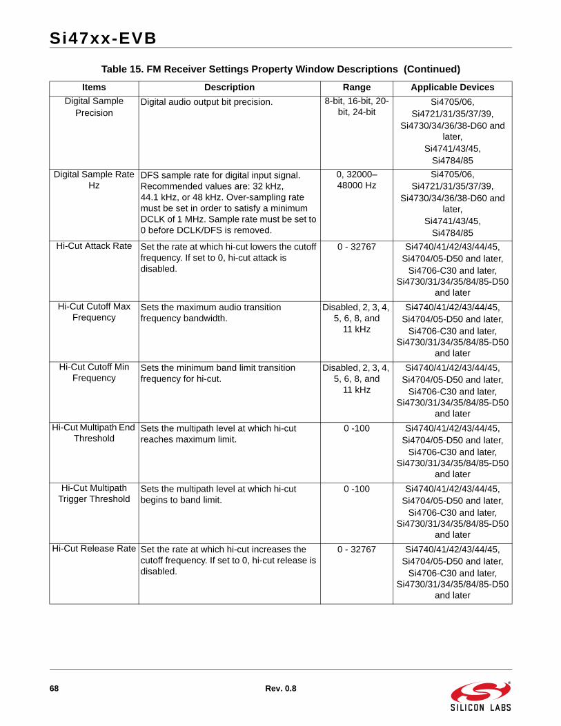
Si47xx-EVB
68 Rev. 0.8
Digital Sample Precision
Digital audio output bit precision. 8-bit, 16-bit, 20-bit, 24-bit
Si4705/06,Si4721/31/35/37/39,
Si4730/34/36/38-D60 and later,
Si4741/43/45,Si4784/85
Digital Sample Rate Hz
DFS sample rate for digital input signal. Recommended values are: 32 kHz, 44.1 kHz, or 48 kHz. Over-sampling rate must be set in order to satisfy a minimum DCLK of 1 MHz. Sample rate must be set to 0 before DCLK/DFS is removed.
0, 32000–48000 Hz
Si4705/06,Si4721/31/35/37/39,
Si4730/34/36/38-D60 and later,
Si4741/43/45,Si4784/85
Hi-Cut Attack Rate Set the rate at which hi-cut lowers the cutoff frequency. If set to 0, hi-cut attack is disabled.
0 - 32767 Si4740/41/42/43/44/45, Si4704/05-D50 and later,
Si4706-C30 and later, Si4730/31/34/35/84/85-D50
and later
Hi-Cut Cutoff Max Frequency
Sets the maximum audio transition frequency bandwidth.
Disabled, 2, 3, 4, 5, 6, 8, and
11 kHz
Si4740/41/42/43/44/45, Si4704/05-D50 and later,
Si4706-C30 and later, Si4730/31/34/35/84/85-D50
and later
Hi-Cut Cutoff Min Frequency
Sets the minimum band limit transition frequency for hi-cut.
Disabled, 2, 3, 4, 5, 6, 8, and
11 kHz
Si4740/41/42/43/44/45, Si4704/05-D50 and later,
Si4706-C30 and later, Si4730/31/34/35/84/85-D50
and later
Hi-Cut Multipath End Threshold
Sets the multipath level at which hi-cut reaches maximum limit.
0 -100 Si4740/41/42/43/44/45, Si4704/05-D50 and later,
Si4706-C30 and later, Si4730/31/34/35/84/85-D50
and later
Hi-Cut Multipath Trigger Threshold
Sets the multipath level at which hi-cut begins to band limit.
0 -100 Si4740/41/42/43/44/45, Si4704/05-D50 and later,
Si4706-C30 and later, Si4730/31/34/35/84/85-D50
and later
Hi-Cut Release Rate Set the rate at which hi-cut increases the cutoff frequency. If set to 0, hi-cut release is disabled.
0 - 32767 Si4740/41/42/43/44/45, Si4704/05-D50 and later,
Si4706-C30 and later, Si4730/31/34/35/84/85-D50
and later
Table 15. FM Receiver Settings Property Window Descriptions (Continued)
Items Description Range Applicable Devices
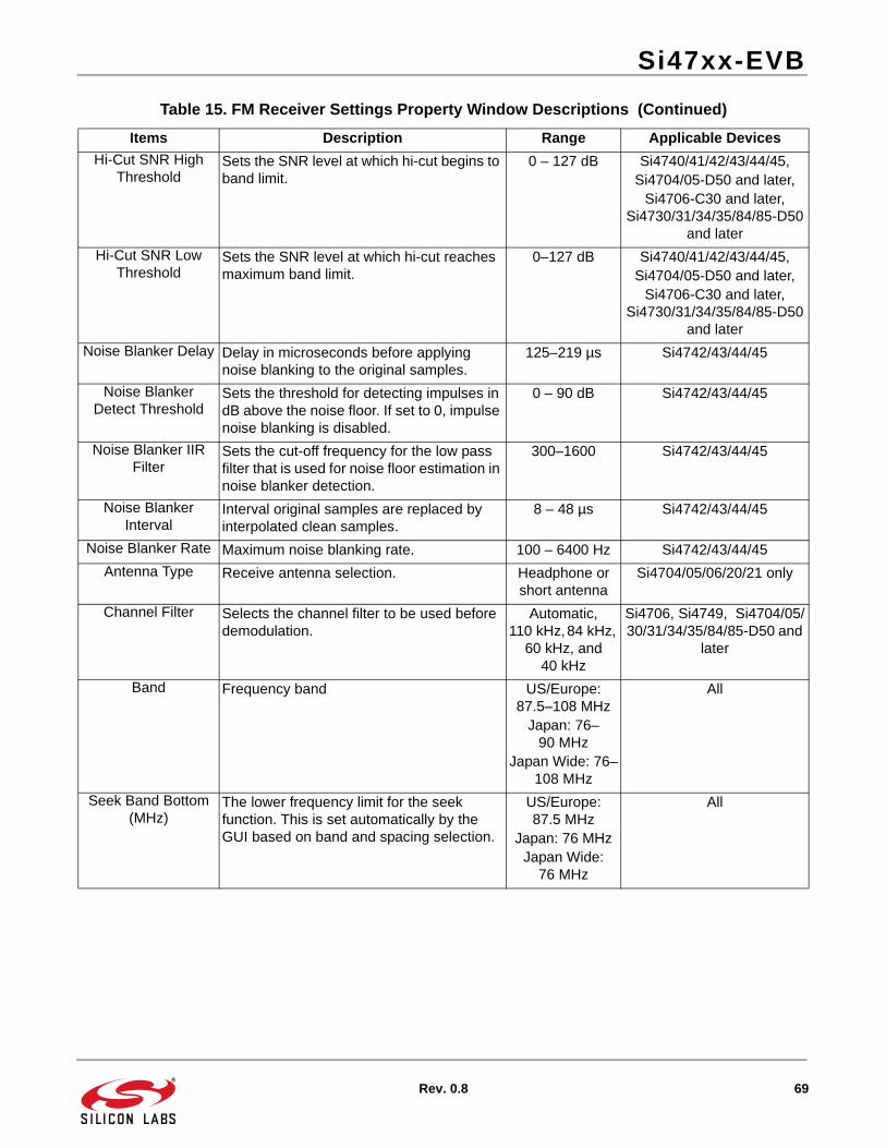
Si47xx-EVB
Rev. 0.8 69
Hi-Cut SNR High Threshold
Sets the SNR level at which hi-cut begins to band limit.
0 – 127 dB Si4740/41/42/43/44/45, Si4704/05-D50 and later,
Si4706-C30 and later, Si4730/31/34/35/84/85-D50
and later
Hi-Cut SNR Low Threshold
Sets the SNR level at which hi-cut reaches maximum band limit.
0–127 dB Si4740/41/42/43/44/45, Si4704/05-D50 and later,
Si4706-C30 and later, Si4730/31/34/35/84/85-D50
and later
Noise Blanker Delay Delay in microseconds before applying noise blanking to the original samples.
125–219 µs Si4742/43/44/45
Noise Blanker Detect Threshold
Sets the threshold for detecting impulses in dB above the noise floor. If set to 0, impulse noise blanking is disabled.
0 – 90 dB Si4742/43/44/45
Noise Blanker IIR Filter
Sets the cut-off frequency for the low pass filter that is used for noise floor estimation in noise blanker detection.
300–1600 Si4742/43/44/45
Noise Blanker Interval
Interval original samples are replaced by interpolated clean samples.
8 – 48 µs Si4742/43/44/45
Noise Blanker Rate Maximum noise blanking rate. 100 – 6400 Hz Si4742/43/44/45
Antenna Type Receive antenna selection. Headphone or short antenna
Si4704/05/06/20/21 only
Channel Filter Selects the channel filter to be used before demodulation.
Automatic, 110 kHz, 84 kHz,
60 kHz, and 40 kHz
Si4706, Si4749, Si4704/05/30/31/34/35/84/85-D50 and
later
Band Frequency band US/Europe: 87.5–108 MHz
Japan: 76–90 MHz
Japan Wide: 76–108 MHz
All
Seek Band Bottom (MHz)
The lower frequency limit for the seek function. This is set automatically by the GUI based on band and spacing selection.
US/Europe: 87.5 MHz
Japan: 76 MHzJapan Wide:
76 MHz
All
Table 15. FM Receiver Settings Property Window Descriptions (Continued)
Items Description Range Applicable Devices
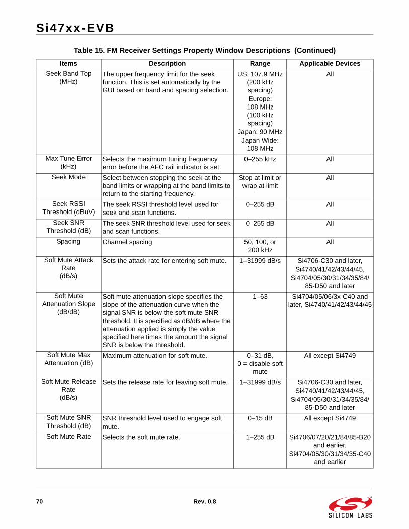
Si47xx-EVB
70 Rev. 0.8
Seek Band Top (MHz)
The upper frequency limit for the seek function. This is set automatically by the GUI based on band and spacing selection.
US: 107.9 MHz (200 kHz spacing)Europe: 108 MHz (100 kHz spacing)
Japan: 90 MHzJapan Wide:
108 MHz
All
Max Tune Error (kHz)
Selects the maximum tuning frequency error before the AFC rail indicator is set.
0–255 kHz All
Seek Mode Select between stopping the seek at the band limits or wrapping at the band limits to return to the starting frequency.
Stop at limit or wrap at limit
All
Seek RSSI Threshold (dBuV)
The seek RSSI threshold level used for seek and scan functions.
0–255 dB All
Seek SNR Threshold (dB)
The seek SNR threshold level used for seek and scan functions.
0–255 dB All
Spacing Channel spacing 50, 100, or 200 kHz
All
Soft Mute Attack Rate(dB/s)
Sets the attack rate for entering soft mute. 1–31999 dB/s Si4706-C30 and later,Si4740/41/42/43/44/45,
Si4704/05/30/31/34/35/84/85-D50 and later
Soft Mute Attenuation Slope
(dB/dB)
Soft mute attenuation slope specifies the slope of the attenuation curve when the signal SNR is below the soft mute SNR threshold. It is specified as dB/dB where the attenuation applied is simply the value specified here times the amount the signal SNR is below the threshold.
1–63 Si4704/05/06/3x-C40 and later, Si4740/41/42/43/44/45
Soft Mute Max Attenuation (dB)
Maximum attenuation for soft mute. 0–31 dB, 0 = disable soft
mute
All except Si4749
Soft Mute Release Rate(dB/s)
Sets the release rate for leaving soft mute. 1–31999 dB/s Si4706-C30 and later,Si4740/41/42/43/44/45,
Si4704/05/30/31/34/35/84/85-D50 and later
Soft Mute SNR Threshold (dB)
SNR threshold level used to engage soft mute.
0–15 dB All except Si4749
Soft Mute Rate Selects the soft mute rate. 1–255 dB Si4706/07/20/21/84/85-B20 and earlier,
Si4704/05/30/31/34/35-C40 and earlier
Table 15. FM Receiver Settings Property Window Descriptions (Continued)
Items Description Range Applicable Devices
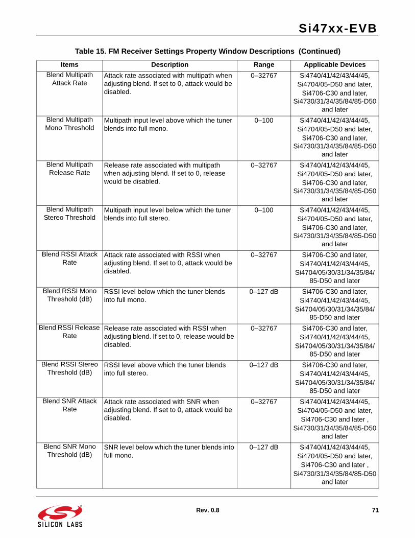
Si47xx-EVB
Rev. 0.8 71
Blend Multipath Attack Rate
Attack rate associated with multipath when adjusting blend. If set to 0, attack would be disabled.
0–32767 Si4740/41/42/43/44/45, Si4704/05-D50 and later,
Si4706-C30 and later, Si4730/31/34/35/84/85-D50
and later
Blend Multipath Mono Threshold
Multipath input level above which the tuner blends into full mono.
0–100 Si4740/41/42/43/44/45, Si4704/05-D50 and later,
Si4706-C30 and later, Si4730/31/34/35/84/85-D50
and later
Blend Multipath Release Rate
Release rate associated with multipath when adjusting blend. If set to 0, release would be disabled.
0–32767 Si4740/41/42/43/44/45, Si4704/05-D50 and later,
Si4706-C30 and later, Si4730/31/34/35/84/85-D50
and later
Blend Multipath Stereo Threshold
Multipath input level below which the tuner blends into full stereo.
0–100 Si4740/41/42/43/44/45, Si4704/05-D50 and later,
Si4706-C30 and later, Si4730/31/34/35/84/85-D50
and later
Blend RSSI Attack Rate
Attack rate associated with RSSI when adjusting blend. If set to 0, attack would be disabled.
0–32767 Si4706-C30 and later,Si4740/41/42/43/44/45,
Si4704/05/30/31/34/35/84/85-D50 and later
Blend RSSI Mono Threshold (dB)
RSSI level below which the tuner blends into full mono.
0–127 dB Si4706-C30 and later,Si4740/41/42/43/44/45,
Si4704/05/30/31/34/35/84/85-D50 and later
Blend RSSI Release Rate
Release rate associated with RSSI when adjusting blend. If set to 0, release would be disabled.
0–32767 Si4706-C30 and later,Si4740/41/42/43/44/45,
Si4704/05/30/31/34/35/84/85-D50 and later
Blend RSSI Stereo Threshold (dB)
RSSI level above which the tuner blends into full stereo.
0–127 dB Si4706-C30 and later,Si4740/41/42/43/44/45,
Si4704/05/30/31/34/35/84/85-D50 and later
Blend SNR Attack Rate
Attack rate associated with SNR when adjusting blend. If set to 0, attack would be disabled.
0–32767 Si4740/41/42/43/44/45,Si4704/05-D50 and later,Si4706-C30 and later ,
Si4730/31/34/35/84/85-D50 and later
Blend SNR Mono Threshold (dB)
SNR level below which the tuner blends into full mono.
0–127 dB Si4740/41/42/43/44/45,Si4704/05-D50 and later,Si4706-C30 and later ,
Si4730/31/34/35/84/85-D50 and later
Table 15. FM Receiver Settings Property Window Descriptions (Continued)
Items Description Range Applicable Devices
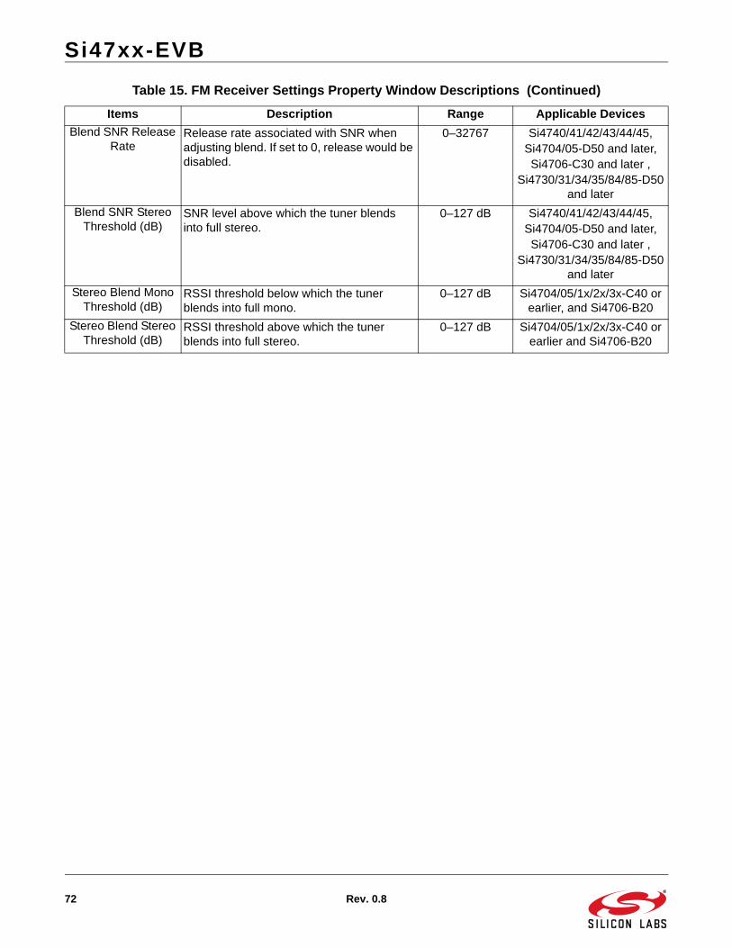
Si47xx-EVB
72 Rev. 0.8
Blend SNR Release Rate
Release rate associated with SNR when adjusting blend. If set to 0, release would be disabled.
0–32767 Si4740/41/42/43/44/45,Si4704/05-D50 and later,Si4706-C30 and later ,
Si4730/31/34/35/84/85-D50 and later
Blend SNR Stereo Threshold (dB)
SNR level above which the tuner blends into full stereo.
0–127 dB Si4740/41/42/43/44/45,Si4704/05-D50 and later,Si4706-C30 and later ,
Si4730/31/34/35/84/85-D50 and later
Stereo Blend Mono Threshold (dB)
RSSI threshold below which the tuner blends into full mono.
0–127 dB Si4704/05/1x/2x/3x-C40 or earlier, and Si4706-B20
Stereo Blend Stereo Threshold (dB)
RSSI threshold above which the tuner blends into full stereo.
0–127 dB Si4704/05/1x/2x/3x-C40 or earlier and Si4706-B20
Table 15. FM Receiver Settings Property Window Descriptions (Continued)
Items Description Range Applicable Devices
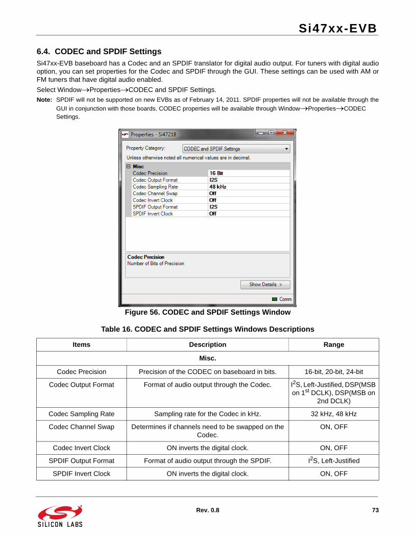
Si47xx-EVB
Rev. 0.8 73
6.4. CODEC and SPDIF SettingsSi47xx-EVB baseboard has a Codec and an SPDIF translator for digital audio output. For tuners with digital audiooption, you can set properties for the Codec and SPDIF through the GUI. These settings can be used with AM orFM tuners that have digital audio enabled.
Select WindowPropertiesCODEC and SPDIF Settings.
Note: SPDIF will not be supported on new EVBs as of February 14, 2011. SPDIF properties will not be available through the
GUI in conjunction with those boards. CODEC properties will be available through WindowPropertiesCODEC Settings.
Figure 56. CODEC and SPDIF Settings Window
Table 16. CODEC and SPDIF Settings Windows Descriptions
Items Description Range
Misc.
Codec Precision Precision of the CODEC on baseboard in bits. 16-bit, 20-bit, 24-bit
Codec Output Format Format of audio output through the Codec. I2S, Left-Justified, DSP(MSB on 1st DCLK), DSP(MSB on
2nd DCLK)
Codec Sampling Rate Sampling rate for the Codec in kHz. 32 kHz, 48 kHz
Codec Channel Swap Determines if channels need to be swapped on the Codec.
ON, OFF
Codec Invert Clock ON inverts the digital clock. ON, OFF
SPDIF Output Format Format of audio output through the SPDIF. I2S, Left-Justified
SPDIF Invert Clock ON inverts the digital clock. ON, OFF
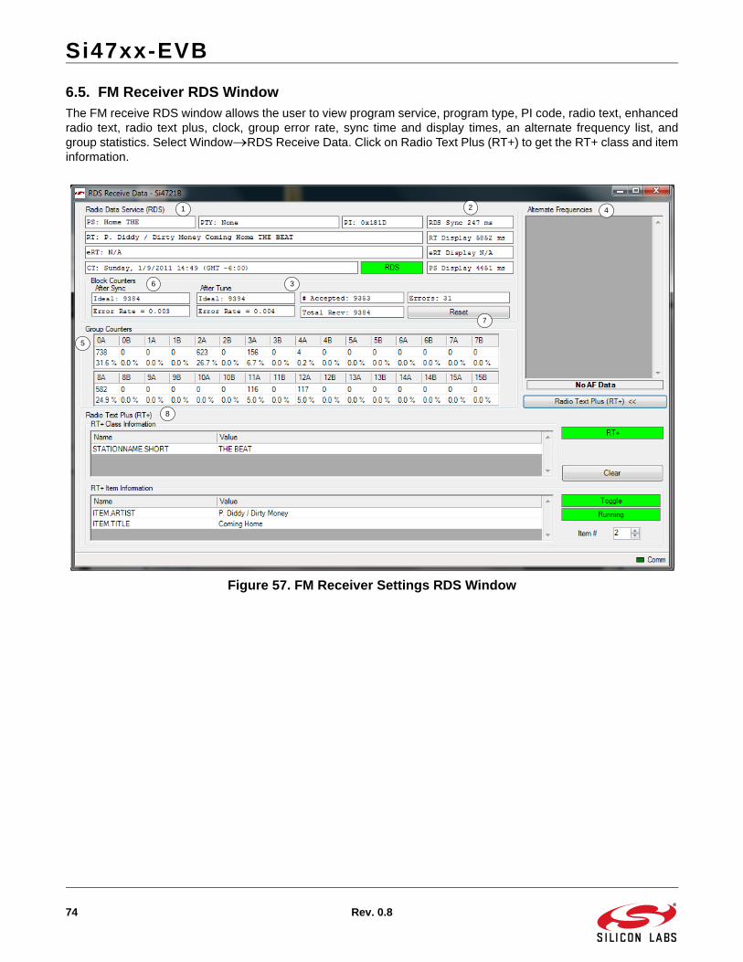
Si47xx-EVB
74 Rev. 0.8
6.5. FM Receiver RDS WindowThe FM receive RDS window allows the user to view program service, program type, PI code, radio text, enhancedradio text, radio text plus, clock, group error rate, sync time and display times, an alternate frequency list, andgroup statistics. Select WindowRDS Receive Data. Click on Radio Text Plus (RT+) to get the RT+ class and iteminformation.
Figure 57. FM Receiver Settings RDS Window
1 2
3
4
5
6
7
8
Si47xx-EVB
Rev. 0.8 75
Table 17. FM Receiver Settings RDS Window Descriptions
# Items Description
1 Radio Data Service PS: Program Service Indicator (8 characters).
RT: Radio Text Indicator (64 characters).
eRT: Enhanced Radio Text Indicator
CT: Clock Indicator showing time, day, and date.
Group Error Rate indicates the percentage of uncorrectable groups received.
PTY: Program Type Indicator
PI: PI Code Indicator
2 Sync Times Time required to synchronize, display radio text, and display program service.
3 RDS Synchronization
Indicator
Indicates that RDS is synchronized.
4 Alternate Frequency Indicator
When present, shows a list of alternate frequencies. Alternate frequency methods A and B are supported.
5 Group Counters Provides the total number and percentage breakdown of group types 0–15, A/B. To view this information, select WindowRDS Group Counters. Please refer to Figure 58.
6 Block Counters Provides the block error rates after tune and after RDS Sync. After Tune Error Rate: After tune (STC interrupt), the ideal number of blocks the FM tuner should have received is calculated. Also, the number of accepted blocks and errors are calculated. Error Rate = number of errors / number of ideal blocks after tune.After Sync Error Rate: After RDS Sync (RDS interrupt), the ideal number of blocks the FM tuner should have received is calculated. Also, the number of accepted blocks and errors are calculated. Error Rate = number of errors / number of ideal blocks after syncBecause it usually takes 100~200ms for the FM tuner to synchronize to RDS data (STC interrupt always comes before RDS interrupt), "After Tune Error Rate" will always be greater than "After Sync Error Rate." After a long time, both error rates should consolidate at similar levels.
7 Reset Resets the block counter numbers.
8 Radio Text Plus Radio Text Plus (RT+) Class and Item Information Indicator
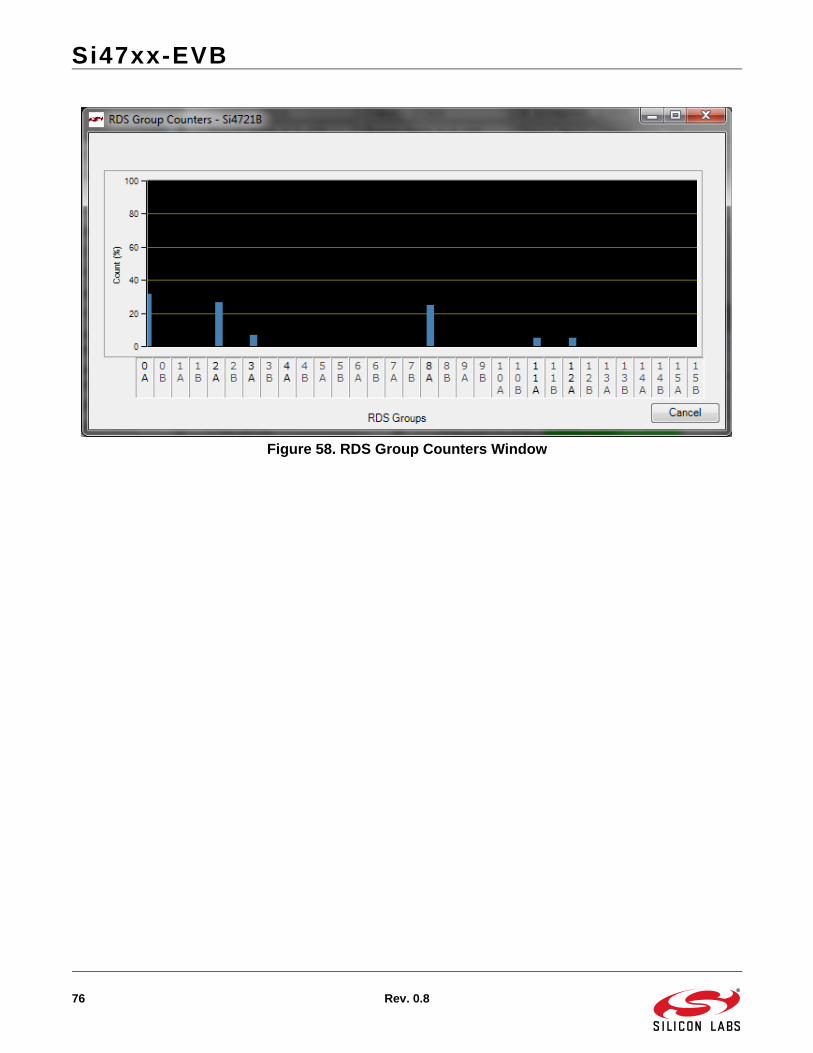
Si47xx-EVB
76 Rev. 0.8
Figure 58. RDS Group Counters Window
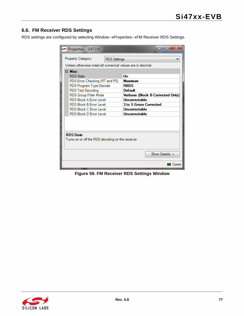
Si47xx-EVB
Rev. 0.8 77
6.6. FM Receiver RDS SettingsRDS settings are configured by selecting WindowPropertiesFM Receiver RDS Settings.
Figure 59. FM Receiver RDS Settings Window
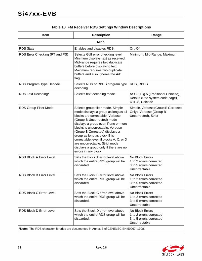
Si47xx-EVB
78 Rev. 0.8
Table 18. FM Receiver RDS Settings Window Descriptions
Item Description Range
Misc.
RDS State Enables and disables RDS. On, Off
RDS Error Checking (RT and PS) Selects GUI error checking level. Minimum displays text as received. Mid-range requires two duplicate buffers before displaying text. Maximum requires two duplicate buffers and also ignores the A/B flag.
Minimum, Mid-Range, Maximum
RDS Program Type Decode Selects RDS or RBDS program type decoding.
RDS, RBDS
RDS Text Decoding* Selects text decoding mode. ASCII, Big 5 (Traditional Chinese), Default (Use system code page), UTF-8, Unicode
RDS Group Filter Mode Selects group filter mode. Simple mode displays a group as long as all blocks are correctable. Verbose (Group B Uncorrected) mode displays a group even if one or more blocks is uncorrectable. Verbose (Group B Corrected) displays a group as long as block B is correctable, even if blocks A, C, or D are uncorrectable. Strict mode displays a group only if there are no errors in any block.
Simple, Verbose (Group B Corrected Only), Verbose (Group B Uncorrected), Strict
RDS Block A Error Level Sets the Block A error level above which the entire RDS group will be discarded.
No Block Errors1 to 2 errors corrected3 to 5 errors correctedUncorrectable
RDS Block B Error Level Sets the Block B error level above which the entire RDS group will be discarded.
No Block Errors1 to 2 errors corrected3 to 5 errors correctedUncorrectable
RDS Block C Error Level Sets the Block C error level above which the entire RDS group will be discarded.
No Block Errors1 to 2 errors corrected3 to 5 errors correctedUncorrectable
RDS Block D Error Level Sets the Block D error level above which the entire RDS group will be discarded.
No Block Errors1 to 2 errors corrected3 to 5 errors correctedUncorrectable
*Note: The RDS character libraries are documented in Annex E of CENELEC EN 50067: 1998.
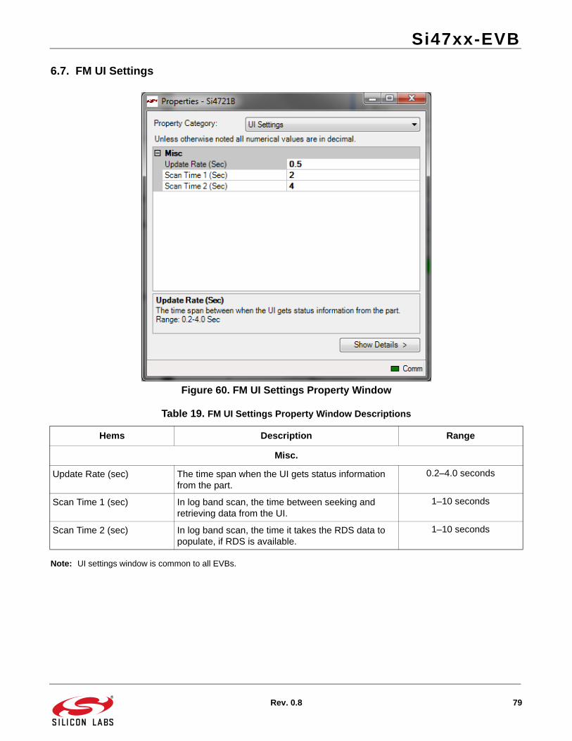
Si47xx-EVB
Rev. 0.8 79
6.7. FM UI Settings
Figure 60. FM UI Settings Property Window
Note: UI settings window is common to all EVBs.
Table 19. FM UI Settings Property Window Descriptions
Hems Description Range
Misc.
Update Rate (sec) The time span when the UI gets status information from the part.
0.2–4.0 seconds
Scan Time 1 (sec) In log band scan, the time between seeking and retrieving data from the UI.
1–10 seconds
Scan Time 2 (sec) In log band scan, the time it takes the RDS data to populate, if RDS is available.
1–10 seconds
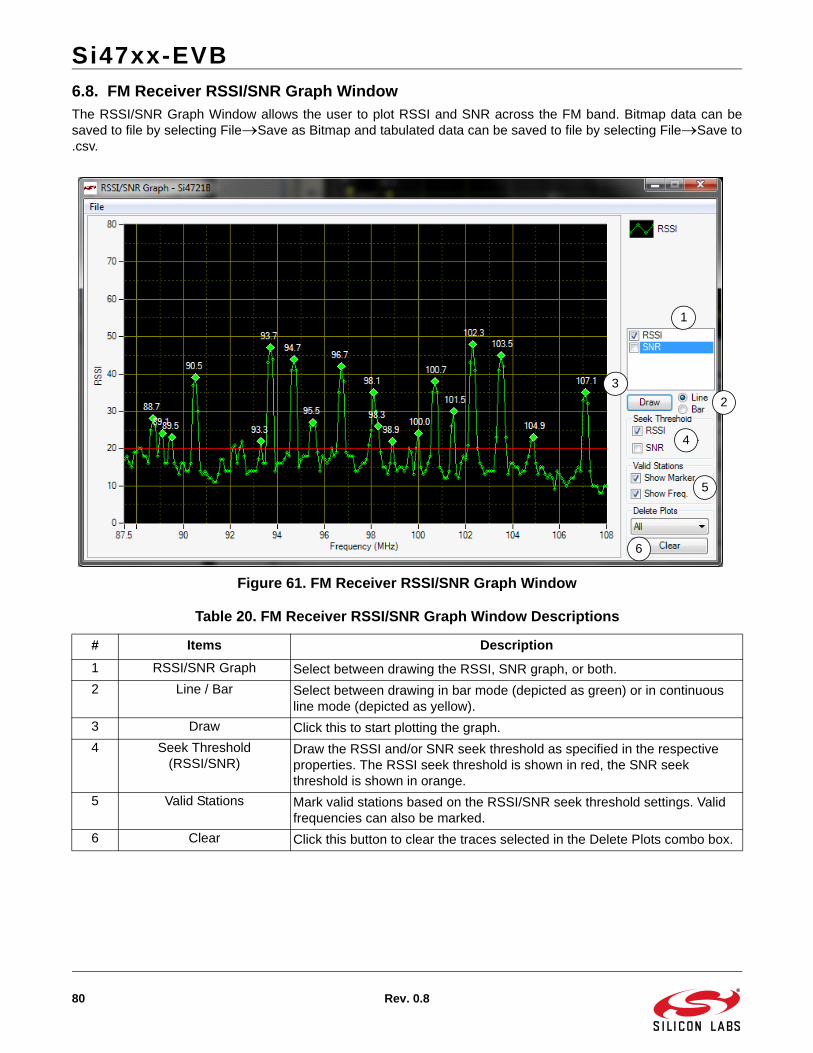
Si47xx-EVB
80 Rev. 0.8
6.8. FM Receiver RSSI/SNR Graph WindowThe RSSI/SNR Graph Window allows the user to plot RSSI and SNR across the FM band. Bitmap data can besaved to file by selecting FileSave as Bitmap and tabulated data can be saved to file by selecting FileSave to.csv.
Figure 61. FM Receiver RSSI/SNR Graph Window
Table 20. FM Receiver RSSI/SNR Graph Window Descriptions
# Items Description
1 RSSI/SNR Graph Select between drawing the RSSI, SNR graph, or both.
2 Line / Bar Select between drawing in bar mode (depicted as green) or in continuous line mode (depicted as yellow).
3 Draw Click this to start plotting the graph.
4 Seek Threshold (RSSI/SNR)
Draw the RSSI and/or SNR seek threshold as specified in the respective properties. The RSSI seek threshold is shown in red, the SNR seek threshold is shown in orange.
5 Valid Stations Mark valid stations based on the RSSI/SNR seek threshold settings. Valid frequencies can also be marked.
6 Clear Click this button to clear the traces selected in the Delete Plots combo box.
1
2
3
4
5
6
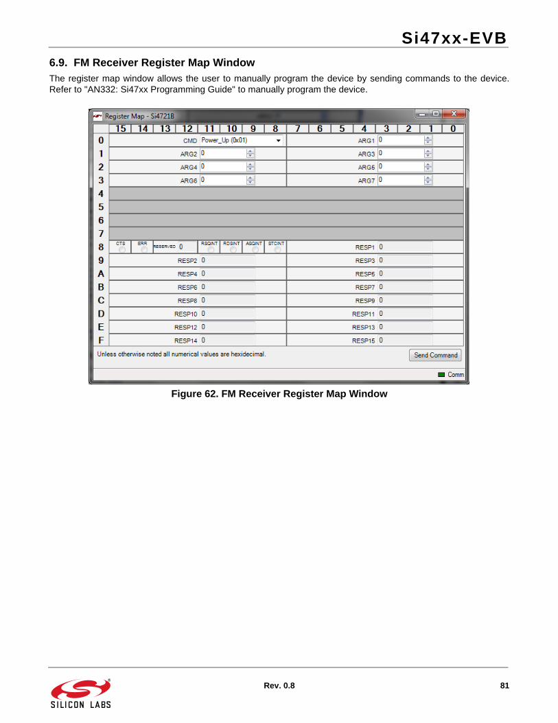
Si47xx-EVB
Rev. 0.8 81
6.9. FM Receiver Register Map WindowThe register map window allows the user to manually program the device by sending commands to the device.Refer to "AN332: Si47xx Programming Guide" to manually program the device.
Figure 62. FM Receiver Register Map Window
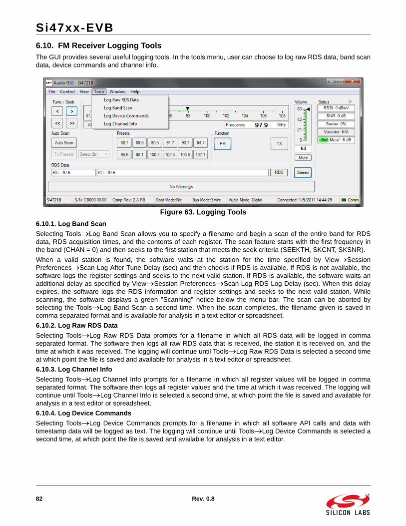
Si47xx-EVB
82 Rev. 0.8
6.10. FM Receiver Logging ToolsThe GUI provides several useful logging tools. In the tools menu, user can choose to log raw RDS data, band scandata, device commands and channel info.
Figure 63. Logging Tools
6.10.1. Log Band Scan
Selecting ToolsLog Band Scan allows you to specify a filename and begin a scan of the entire band for RDSdata, RDS acquisition times, and the contents of each register. The scan feature starts with the first frequency inthe band (CHAN = 0) and then seeks to the first station that meets the seek criteria (SEEKTH, SKCNT, SKSNR).
When a valid station is found, the software waits at the station for the time specified by ViewSessionPreferencesScan Log After Tune Delay (sec) and then checks if RDS is available. If RDS is not available, thesoftware logs the register settings and seeks to the next valid station. If RDS is available, the software waits anadditional delay as specified by ViewSession PreferencesScan Log RDS Log Delay (sec). When this delayexpires, the software logs the RDS information and register settings and seeks to the next valid station. Whilescanning, the software displays a green "Scanning" notice below the menu bar. The scan can be aborted byselecting the ToolsLog Band Scan a second time. When the scan completes, the filename given is saved incomma separated format and is available for analysis in a text editor or spreadsheet.
6.10.2. Log Raw RDS Data
Selecting ToolsLog Raw RDS Data prompts for a filename in which all RDS data will be logged in commaseparated format. The software then logs all raw RDS data that is received, the station it is received on, and thetime at which it was received. The logging will continue until ToolsLog Raw RDS Data is selected a second timeat which point the file is saved and available for analysis in a text editor or spreadsheet.
6.10.3. Log Channel Info
Selecting ToolsLog Channel Info prompts for a filename in which all register values will be logged in commaseparated format. The software then logs all register values and the time at which it was received. The logging willcontinue until ToolsLog Channel Info is selected a second time, at which point the file is saved and available foranalysis in a text editor or spreadsheet.
6.10.4. Log Device Commands
Selecting ToolsLog Device Commands prompts for a filename in which all software API calls and data withtimestamp data will be logged as text. The logging will continue until ToolsLog Device Commands is selected asecond time, at which point the file is saved and available for analysis in a text editor.
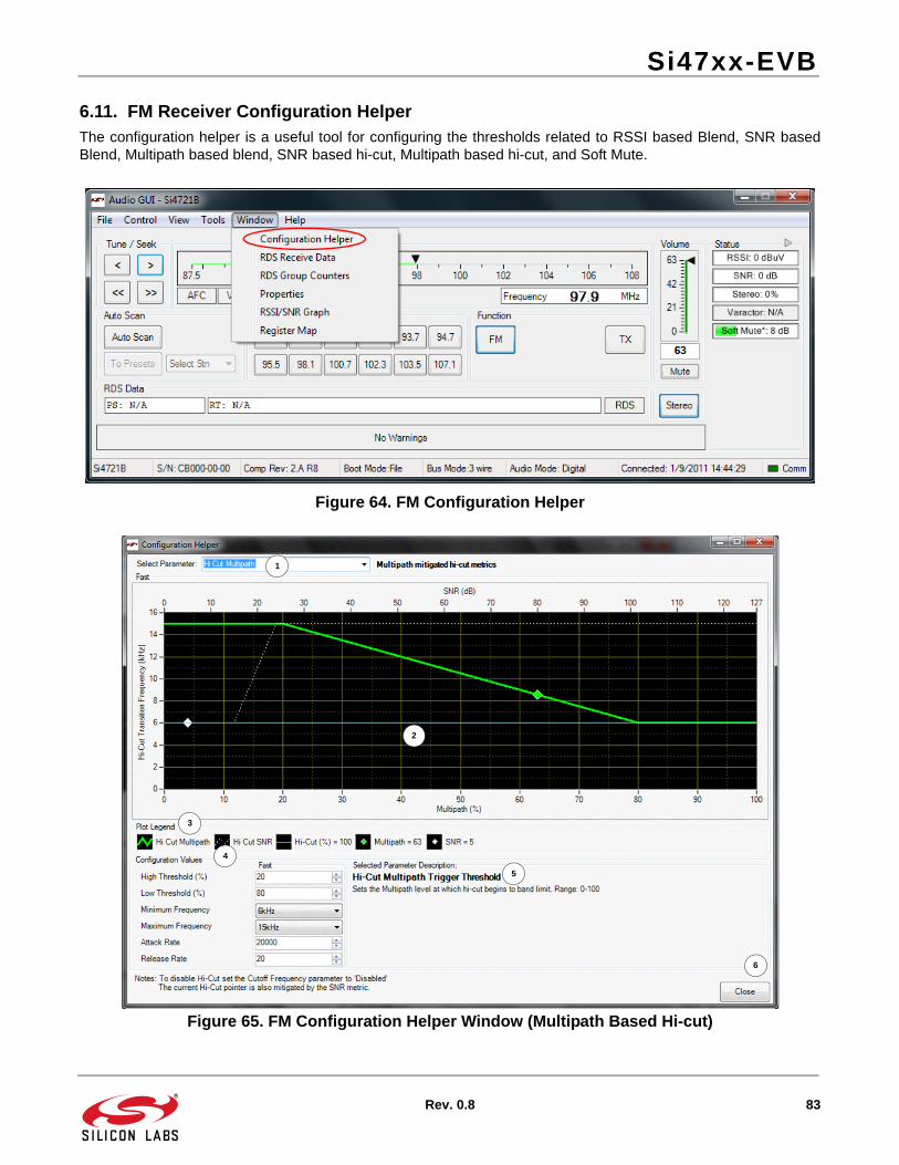
Si47xx-EVB
Rev. 0.8 83
6.11. FM Receiver Configuration HelperThe configuration helper is a useful tool for configuring the thresholds related to RSSI based Blend, SNR basedBlend, Multipath based blend, SNR based hi-cut, Multipath based hi-cut, and Soft Mute.
Figure 64. FM Configuration Helper
Figure 65. FM Configuration Helper Window (Multipath Based Hi-cut)
1
2
3
4
5
6
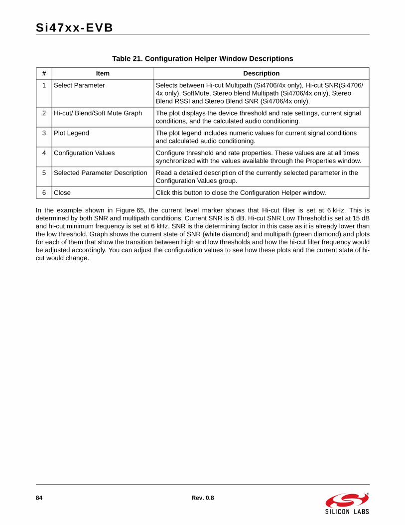
Si47xx-EVB
84 Rev. 0.8
In the example shown in Figure 65, the current level marker shows that Hi-cut filter is set at 6 kHz. This isdetermined by both SNR and multipath conditions. Current SNR is 5 dB. Hi-cut SNR Low Threshold is set at 15 dBand hi-cut minimum frequency is set at 6 kHz. SNR is the determining factor in this case as it is already lower thanthe low threshold. Graph shows the current state of SNR (white diamond) and multipath (green diamond) and plotsfor each of them that show the transition between high and low thresholds and how the hi-cut filter frequency wouldbe adjusted accordingly. You can adjust the configuration values to see how these plots and the current state of hi-cut would change.
Table 21. Configuration Helper Window Descriptions
# Item Description
1 Select Parameter Selects between Hi-cut Multipath (Si4706/4x only), Hi-cut SNR(Si4706/4x only), SoftMute, Stereo blend Multipath (Si4706/4x only), Stereo Blend RSSI and Stereo Blend SNR (Si4706/4x only).
2 Hi-cut/ Blend/Soft Mute Graph The plot displays the device threshold and rate settings, current signal conditions, and the calculated audio conditioning.
3 Plot Legend The plot legend includes numeric values for current signal conditions and calculated audio conditioning.
4 Configuration Values Configure threshold and rate properties. These values are at all times synchronized with the values available through the Properties window.
5 Selected Parameter Description Read a detailed description of the currently selected parameter in the Configuration Values group.
6 Close Click this button to close the Configuration Helper window.
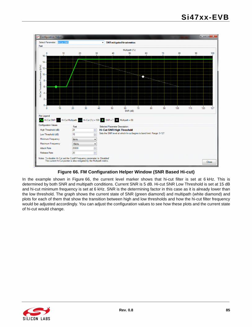
Si47xx-EVB
Rev. 0.8 85
Figure 66. FM Configuration Helper Window (SNR Based Hi-cut)
In the example shown in Figure 66, the current level marker shows that hi-cut filter is set at 6 kHz. This isdetermined by both SNR and multipath conditions. Current SNR is 5 dB. Hi-cut SNR Low Threshold is set at 15 dBand hi-cut minimum frequency is set at 6 kHz. SNR is the determining factor in this case as it is already lower thanthe low threshold. The graph shows the current state of SNR (green diamond) and multipath (white diamond) andplots for each of them that show the transition between high and low thresholds and how the hi-cut filter frequencywould be adjusted accordingly. You can adjust the configuration values to see how these plots and the current stateof hi-cut would change.
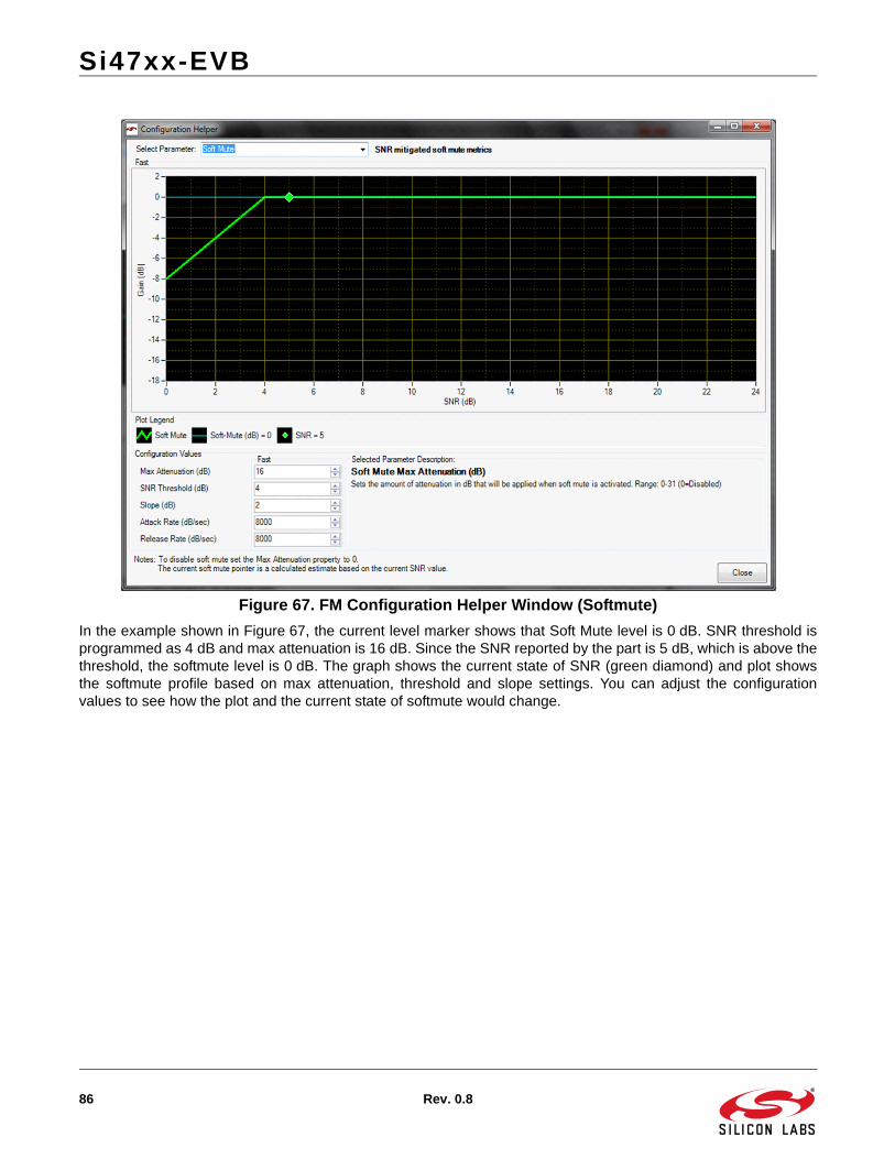
Si47xx-EVB
86 Rev. 0.8
Figure 67. FM Configuration Helper Window (Softmute)
In the example shown in Figure 67, the current level marker shows that Soft Mute level is 0 dB. SNR threshold isprogrammed as 4 dB and max attenuation is 16 dB. Since the SNR reported by the part is 5 dB, which is above thethreshold, the softmute level is 0 dB. The graph shows the current state of SNR (green diamond) and plot showsthe softmute profile based on max attenuation, threshold and slope settings. You can adjust the configurationvalues to see how the plot and the current state of softmute would change.
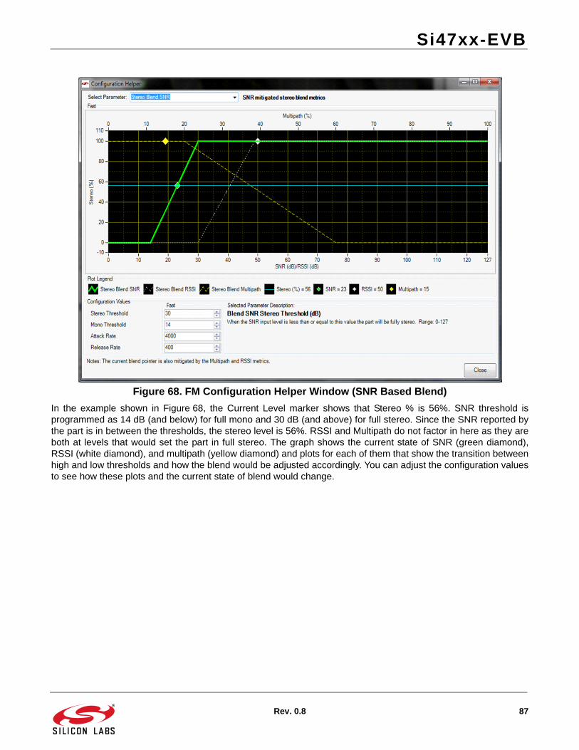
Si47xx-EVB
Rev. 0.8 87
Figure 68. FM Configuration Helper Window (SNR Based Blend)
In the example shown in Figure 68, the Current Level marker shows that Stereo % is 56%. SNR threshold isprogrammed as 14 dB (and below) for full mono and 30 dB (and above) for full stereo. Since the SNR reported bythe part is in between the thresholds, the stereo level is 56%. RSSI and Multipath do not factor in here as they areboth at levels that would set the part in full stereo. The graph shows the current state of SNR (green diamond),RSSI (white diamond), and multipath (yellow diamond) and plots for each of them that show the transition betweenhigh and low thresholds and how the blend would be adjusted accordingly. You can adjust the configuration valuesto see how these plots and the current state of blend would change.
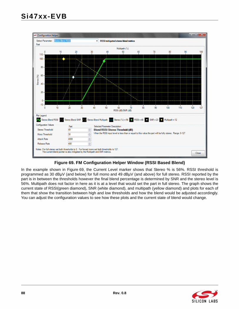
Si47xx-EVB
88 Rev. 0.8
Figure 69. FM Configuration Helper Window (RSSI Based Blend)
In the example shown in Figure 69, the Current Level marker shows that Stereo % is 56%. RSSI threshold isprogrammed as 30 dBµV (and below) for full mono and 49 dBµV (and above) for full stereo. RSSI reported by thepart is in between the thresholds however the final blend percentage is determined by SNR and the stereo level is56%. Multipath does not factor in here as it is at a level that would set the part in full stereo. The graph shows thecurrent state of RSSI(green diamond), SNR (white diamond), and multipath (yellow diamond) and plots for each ofthem that show the transition between high and low thresholds and how the blend would be adjusted accordingly.You can adjust the configuration values to see how these plots and the current state of blend would change.
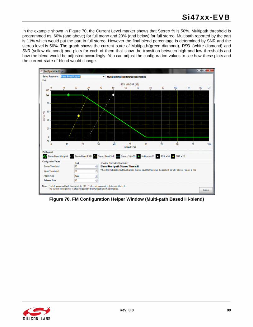
Si47xx-EVB
Rev. 0.8 89
In the example shown in Figure 70, the Current Level marker shows that Stereo % is 50%. Multipath threshold isprogrammed as: 60% (and above) for full mono and 20% (and below) for full stereo. Multipath reported by the partis 11% which would put the part in full stereo. However the final blend percentage is determined by SNR and thestereo level is 56%. The graph shows the current state of Multipath(green diamond), RSSI (white diamond) andSNR (yellow diamond) and plots for each of them that show the transition between high and low thresholds andhow the blend would be adjusted accordingly. You can adjust the configuration values to see how these plots andthe current state of blend would change.
Figure 70. FM Configuration Helper Window (Multi-path Based Hi-blend)

Si47xx-EVB
90 Rev. 0.8
7. Weather Band GUI
7.1. WB Receiver InitializationThe first Si47xx window is the Initialization window as shown in Figure 71. On the function menu, select andhighlight the function of the Si47xx as a WB Receiver. Select the Boot Mode, Audio Mode, Firmware, Bus Mode,and initial part settings and then click Initialize. A new window displaying "Initializing WB Receiver" will appear. Ifyou check "Use XOSCEN," the daughter card crystal and on-chip oscillator will be used to clock the Si47xx. Youcan also select "(Analog Mode) to Analog Output", "(Digital Mode) to SPDIF and CODEC (Analog Output)", or"(Analog & Digital Mode) to Analog Output and SPDIF" with the Audio Mode drop down menu.
Note: SPDIF will not be supported on new EVBs as of February 14, 2011. Modes of operation requiring the SPDIF will not beavailable in the initialization window for those boards.
Figure 71. Weather Band Receiver Initialization
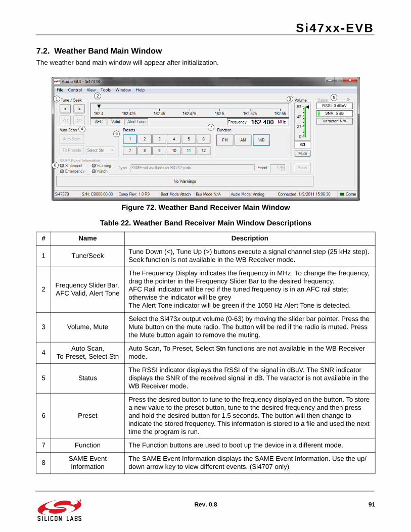
Si47xx-EVB
Rev. 0.8 91
7.2. Weather Band Main WindowThe weather band main window will appear after initialization.
Figure 72. Weather Band Receiver Main Window
Table 22. Weather Band Receiver Main Window Descriptions
# Name Description
1 Tune/SeekTune Down (<), Tune Up (>) buttons execute a signal channel step (25 kHz step). Seek function is not available in the WB Receiver mode.
2Frequency Slider Bar, AFC Valid, Alert Tone
The Frequency Display indicates the frequency in MHz. To change the frequency, drag the pointer in the Frequency Slider Bar to the desired frequency. AFC Rail indicator will be red if the tuned frequency is in an AFC rail state; otherwise the indicator will be greyThe Alert Tone indicator will be green if the 1050 Hz Alert Tone is detected.
3 Volume, MuteSelect the Si473x output volume (0-63) by moving the slider bar pointer. Press the Mute button on the mute radio. The button will be red if the radio is muted. Press the Mute button again to remove the muting.
4Auto Scan,
To Preset, Select StnAuto Scan, To Preset, Select Stn functions are not available in the WB Receiver mode.
5 StatusThe RSSI indicator displays the RSSI of the signal in dBuV. The SNR indicator displays the SNR of the received signal in dB. The varactor is not available in the WB Receiver mode.
6 Preset
Press the desired button to tune to the frequency displayed on the button. To store a new value to the preset button, tune to the desired frequency and then press and hold the desired button for 1.5 seconds. The button will then change to indicate the stored frequency. This information is stored to a file and used the next time the program is run.
7 Function The Function buttons are used to boot up the device in a different mode.
8SAME Event Information
The SAME Event Information displays the SAME Event Information. Use the up/down arrow key to view different events. (Si4707 only)
12
3
4
5
6
7
8
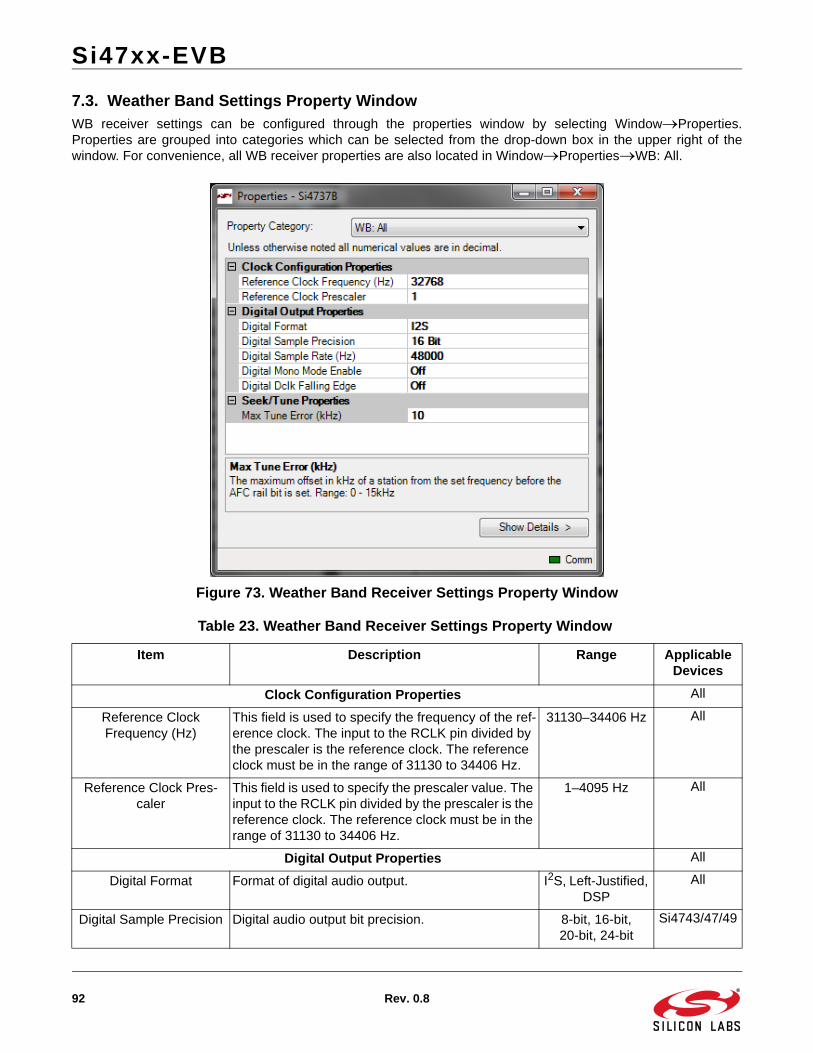
Si47xx-EVB
92 Rev. 0.8
7.3. Weather Band Settings Property WindowWB receiver settings can be configured through the properties window by selecting WindowProperties.Properties are grouped into categories which can be selected from the drop-down box in the upper right of thewindow. For convenience, all WB receiver properties are also located in WindowPropertiesWB: All.
Figure 73. Weather Band Receiver Settings Property Window
Table 23. Weather Band Receiver Settings Property Window
Item Description Range Applicable Devices
Clock Configuration Properties All
Reference Clock Frequency (Hz)
This field is used to specify the frequency of the ref-erence clock. The input to the RCLK pin divided by the prescaler is the reference clock. The reference clock must be in the range of 31130 to 34406 Hz.
31130–34406 Hz All
Reference Clock Pres-caler
This field is used to specify the prescaler value. The input to the RCLK pin divided by the prescaler is the reference clock. The reference clock must be in the range of 31130 to 34406 Hz.
1–4095 Hz All
Digital Output Properties All
Digital Format Format of digital audio output. I2S, Left-Justified, DSP
All
Digital Sample Precision Digital audio output bit precision. 8-bit, 16-bit, 20-bit, 24-bit
Si4743/47/49
Si47xx-EVB
Rev. 0.8 93
Digital Sample Rate Hz DFS sample rate for digital input signal. Recom-mended values are: 32 kHz, 44.1 kHz, or 48 kHz. Over-sampling rate must be set in order to satisfy a minimum DCLK of 1MHz. Sample rate must be set to 0 before DCLK/DFS is removed.
0, 32000–48000 Hz
All
Digital Mono Mode Enable
ON enables mono in digital audio output. ON, OFF All
Digital DCLK Falling Edge ON uses falling edge of DCLK for sampling. ON, OFF All
Seek/Tune Properties All
Max Time Error (kHz) If a station is offset from the set frequency by this amount or more, the AFC rail bit is set.
1–15 kHz All
Table 23. Weather Band Receiver Settings Property Window (Continued)
Item Description Range Applicable Devices
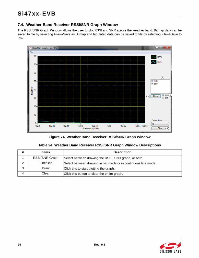
Si47xx-EVB
94 Rev. 0.8
7.4. Weather Band Receiver RSSI/SNR Graph WindowThe RSSI/SNR Graph Window allows the user to plot RSSI and SNR across the weather band. Bitmap data can besaved to file by selecting FileSave as Bitmap and tabulated data can be saved to file by selecting FileSave to.csv.
Figure 74. Weather Band Receiver RSSI/SNR Graph Window
Table 24. Weather Band Receiver RSSI/SNR Graph Window Descriptions
# Items Description
1 RSSI/SNR Graph Select between drawing the RSSI, SNR graph, or both.
2 Line/Bar Select between drawing in bar mode or in continuous line mode.
3 Draw Click this to start plotting the graph.
4 Clear Click this button to clear the entire graph.
1
23
4
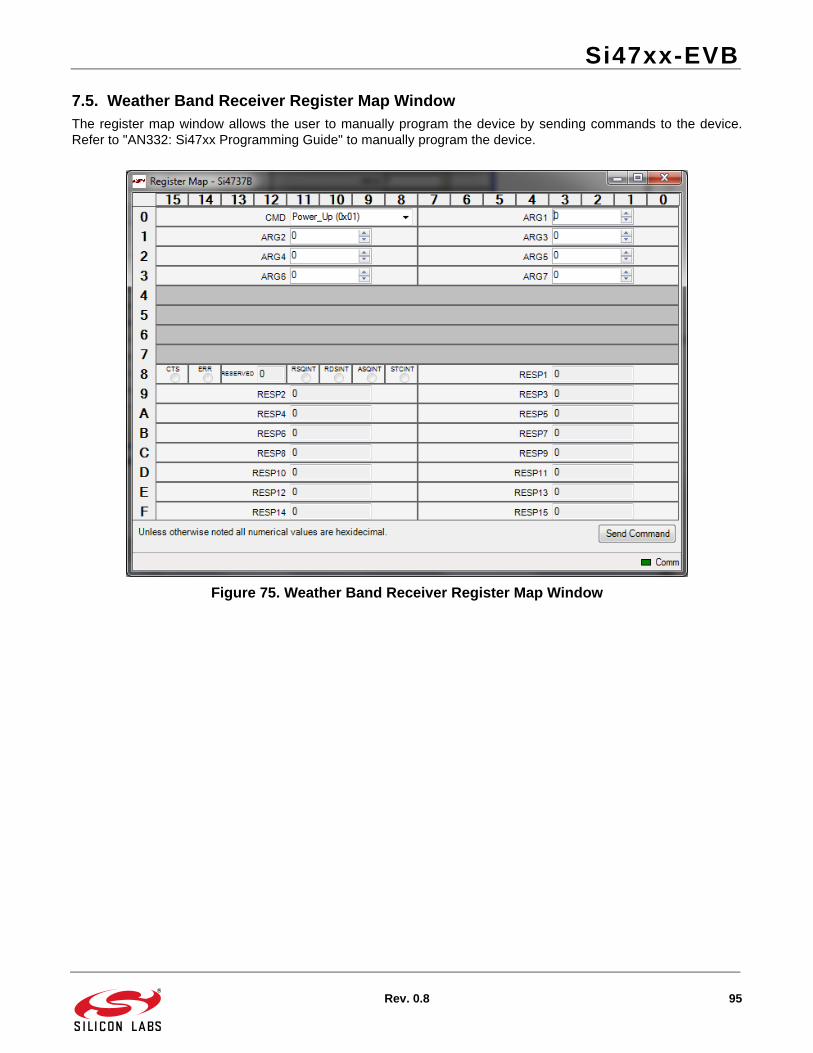
Si47xx-EVB
Rev. 0.8 95
7.5. Weather Band Receiver Register Map WindowThe register map window allows the user to manually program the device by sending commands to the device.Refer to "AN332: Si47xx Programming Guide" to manually program the device.
Figure 75. Weather Band Receiver Register Map Window
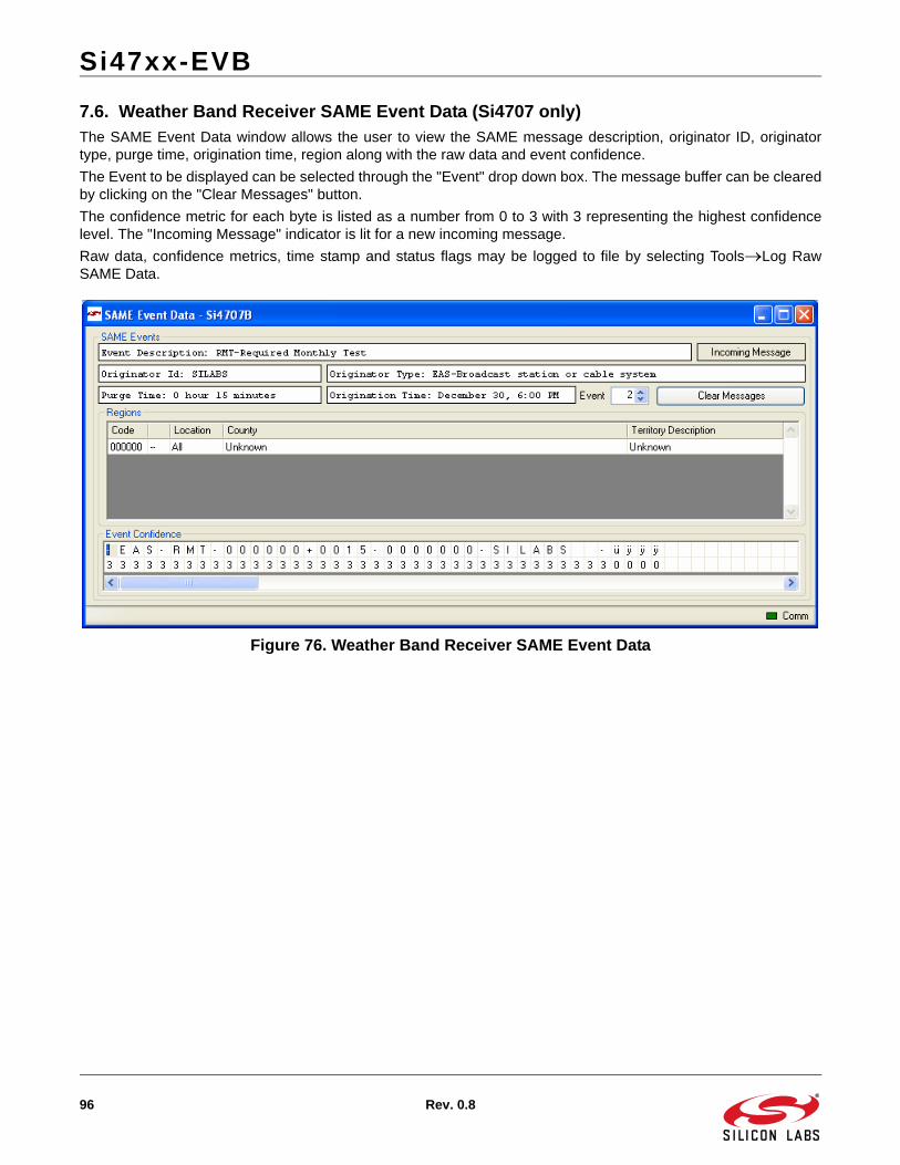
Si47xx-EVB
96 Rev. 0.8
7.6. Weather Band Receiver SAME Event Data (Si4707 only)The SAME Event Data window allows the user to view the SAME message description, originator ID, originatortype, purge time, origination time, region along with the raw data and event confidence.
The Event to be displayed can be selected through the "Event" drop down box. The message buffer can be clearedby clicking on the "Clear Messages" button.
The confidence metric for each byte is listed as a number from 0 to 3 with 3 representing the highest confidencelevel. The "Incoming Message" indicator is lit for a new incoming message.
Raw data, confidence metrics, time stamp and status flags may be logged to file by selecting ToolsLog RawSAME Data.
Figure 76. Weather Band Receiver SAME Event Data
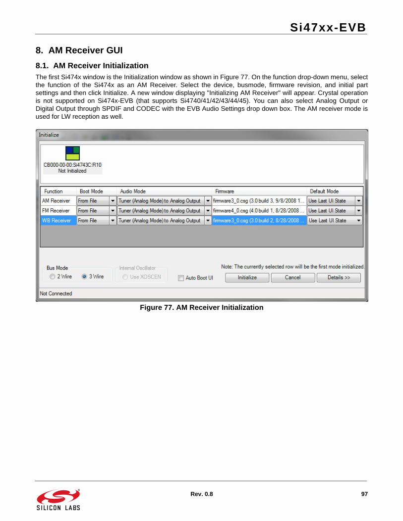
Si47xx-EVB
Rev. 0.8 97
8. AM Receiver GUI
8.1. AM Receiver InitializationThe first Si474x window is the Initialization window as shown in Figure 77. On the function drop-down menu, selectthe function of the Si474x as an AM Receiver. Select the device, busmode, firmware revision, and initial partsettings and then click Initialize. A new window displaying "Initializing AM Receiver" will appear. Crystal operationis not supported on Si474x-EVB (that supports Si4740/41/42/43/44/45). You can also select Analog Output orDigital Output through SPDIF and CODEC with the EVB Audio Settings drop down box. The AM receiver mode isused for LW reception as well.
Figure 77. AM Receiver Initialization

Si47xx-EVB
98 Rev. 0.8
8.2. AM Receiver Main WindowThe AM receiver main window will appear after initialization.
Figure 78. AM Receiver Window
Table 25. AM Receiver Window Descriptions
# Name Description
1 Tune/Seek Tune Down (<), Tune Up (>) buttons execute a single channel step according to the channel spacing setting. The channel spacing setting can be set in the property window.Seek down (<<), Seek Up (>>) buttons execute a seek up or down to the next received FM signal meeting or exceeding the seek settings within the selected band. The seek setting RSSI and SNR threshold can be set in the property window.
2 Frequency Slider
Bar, AFC, Valid
The Frequency Display indicates the frequency in kHz. To change the Frequency, drag the pointer in the Frequency Slider Bar to the desired frequency.AFC Rail indicator will be red if the tuned frequency is in an AFC rail state, otherwise the indicator will be grey.The Valid indicator will be green if the AM frequency meets the RSSI and SNR seek settings.
3 Volume, Mute
Select the Si473x output volume (0–63) by moving the slider bar pointer. Press the Mute button to mute the radio. If the radio is muted the button will be red. Press the Mute button again to remove the muting.
4 Auto Scan The Auto Scan button will find all the stations with an RSSI and SNR above the seek settings in the property window. After the scan is completed, the number of stations found will be displayed and each station will be available in the drop down box. Also, a red indicator mark will be dis-played on the Frequency Slider Bar (2) for each station. The "To Presets" Button will program the preset buttons (5) with the 12 strongest stations.
5 Presets Press the desired button to tune to the frequency displayed on the button. To store a new value to the preset button, tune to the desired frequency and then press and hold the desired button for 1.5 seconds. The button will then change to indicate the stored frequency. This information is stored to a file and used the next time the program is run.
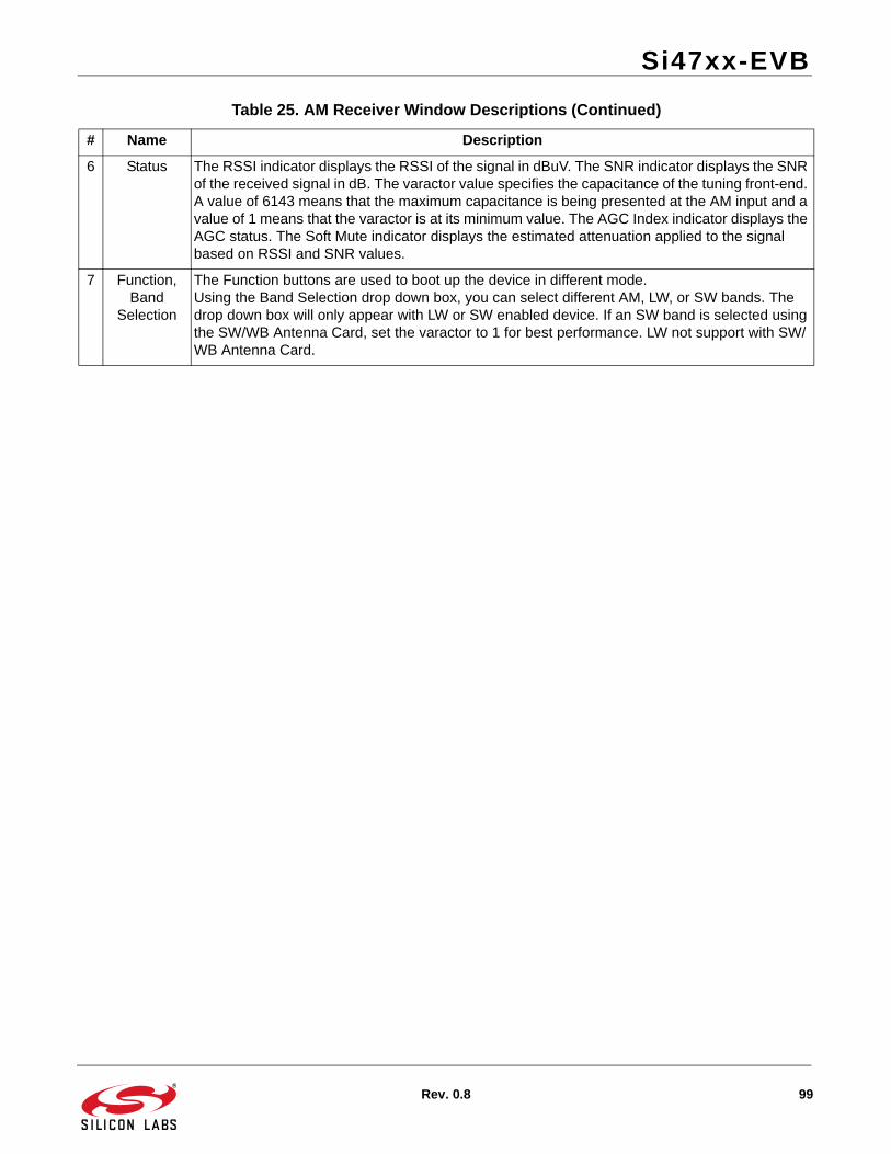
Si47xx-EVB
Rev. 0.8 99
6 Status The RSSI indicator displays the RSSI of the signal in dBuV. The SNR indicator displays the SNR of the received signal in dB. The varactor value specifies the capacitance of the tuning front-end. A value of 6143 means that the maximum capacitance is being presented at the AM input and a value of 1 means that the varactor is at its minimum value. The AGC Index indicator displays the AGC status. The Soft Mute indicator displays the estimated attenuation applied to the signal based on RSSI and SNR values.
7 Function, Band
Selection
The Function buttons are used to boot up the device in different mode. Using the Band Selection drop down box, you can select different AM, LW, or SW bands. The drop down box will only appear with LW or SW enabled device. If an SW band is selected using the SW/WB Antenna Card, set the varactor to 1 for best performance. LW not support with SW/WB Antenna Card.
Table 25. AM Receiver Window Descriptions (Continued)
# Name Description
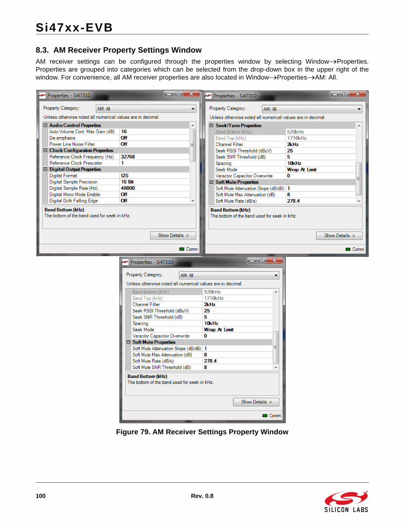
Si47xx-EVB
100 Rev. 0.8
8.3. AM Receiver Property Settings WindowAM receiver settings can be configured through the properties window by selecting WindowProperties.Properties are grouped into categories which can be selected from the drop-down box in the upper right of thewindow. For convenience, all AM receiver properties are also located in WindowPropertiesAM: All.
Figure 79. AM Receiver Settings Property Window
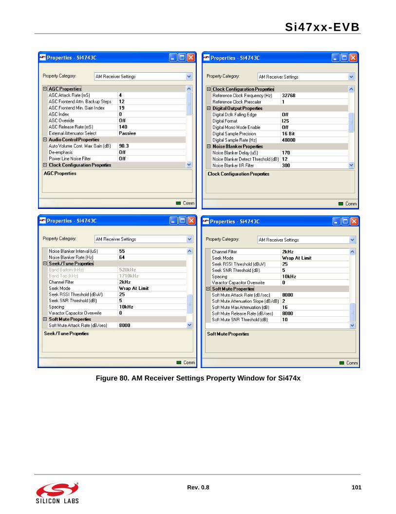
Si47xx-EVB
Rev. 0.8 101
Figure 80. AM Receiver Settings Property Window for Si474x
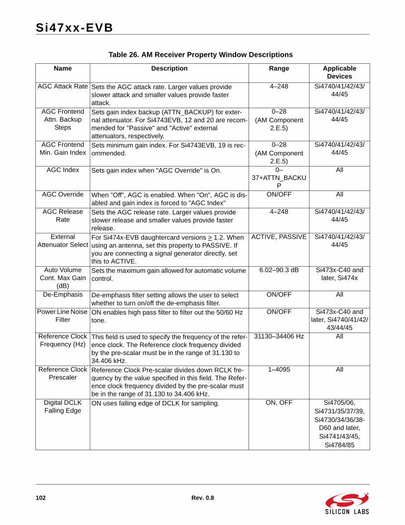
Si47xx-EVB
102 Rev. 0.8
Table 26. AM Receiver Property Window Descriptions
Name Description Range Applicable Devices
AGC Attack Rate Sets the AGC attack rate. Larger values provide slower attack and smaller values provide faster attack.
4–248 Si4740/41/42/43/44/45
AGC Frontend Attn. Backup
Steps
Sets gain index backup (ATTN_BACKUP) for exter-nal attenuator. For Si4743EVB, 12 and 20 are recom-mended for "Passive" and "Active" external attenuators, respectively.
0–28(AM Component
2.E.5)
Si4740/41/42/43/44/45
AGC Frontend Min. Gain Index
Sets minimum gain index. For Si4743EVB, 19 is rec-ommended.
0–28(AM Component
2.E.5)
Si4740/41/42/43/44/45
AGC Index Sets gain index when "AGC Override" is On. 0–37+ATTN_BACKU
P
All
AGC Override When "Off", AGC is enabled. When "On", AGC is dis-abled and gain index is forced to "AGC Index"
ON/OFF All
AGC Release Rate
Sets the AGC release rate. Larger values provide slower release and smaller values provide faster release.
4–248 Si4740/41/42/43/44/45
External Attenuator Select
For Si474x-EVB daughtercard versions > 1.2. When using an antenna, set this property to PASSIVE. If you are connecting a signal generator directly, set this to ACTIVE.
ACTIVE, PASSIVE Si4740/41/42/43/44/45
Auto Volume Cont. Max Gain
(dB)
Sets the maximum gain allowed for automatic volume control.
6.02–90.3 dB Si473x-C40 and later, Si474x
De-Emphasis De-emphasis filter setting allows the user to select whether to turn on/off the de-emphasis filter.
ON/OFF All
Power Line Noise Filter
ON enables high pass filter to filter out the 50/60 Hz tone.
ON/OFF Si473x-C40 and later, Si4740/41/42/
43/44/45Reference Clock Frequency (Hz)
This field is used to specify the frequency of the refer-ence clock. The Reference clock frequency divided by the pre-scalar must be in the range of 31.130 to 34.406 kHz.
31130–34406 Hz All
Reference Clock Prescaler
Reference Clock Pre-scalar divides down RCLK fre-quency by the value specified in this field. The Refer-ence clock frequency divided by the pre-scalar must be in the range of 31.130 to 34.406 kHz.
1–4095 All
Digital DCLK Falling Edge
ON uses falling edge of DCLK for sampling. ON, OFF Si4705/06,Si4731/35/37/39,Si4730/34/36/38-
D60 and later,Si4741/43/45,
Si4784/85
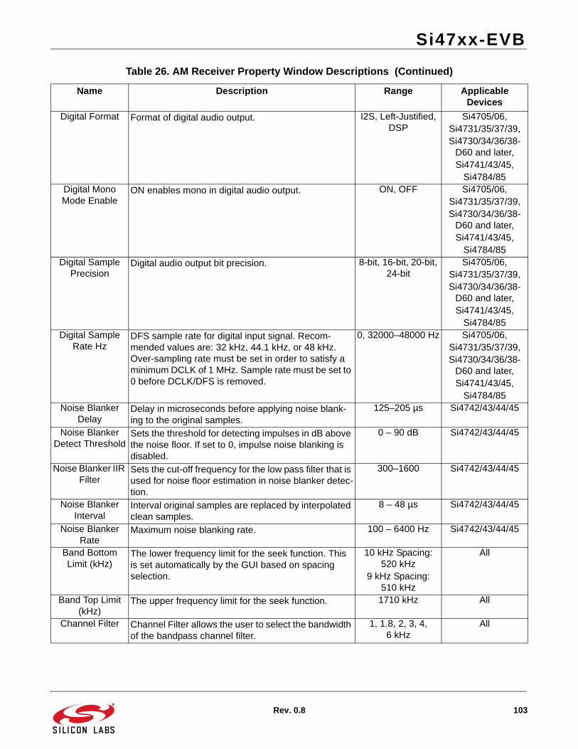
Si47xx-EVB
Rev. 0.8 103
Digital Format Format of digital audio output. I2S, Left-Justified, DSP
Si4705/06,Si4731/35/37/39,Si4730/34/36/38-
D60 and later,Si4741/43/45,
Si4784/85Digital Mono Mode Enable
ON enables mono in digital audio output. ON, OFF Si4705/06,Si4731/35/37/39,Si4730/34/36/38-
D60 and later,Si4741/43/45,
Si4784/85Digital Sample
PrecisionDigital audio output bit precision. 8-bit, 16-bit, 20-bit,
24-bitSi4705/06,
Si4731/35/37/39,Si4730/34/36/38-
D60 and later,Si4741/43/45,
Si4784/85Digital Sample
Rate HzDFS sample rate for digital input signal. Recom-mended values are: 32 kHz, 44.1 kHz, or 48 kHz. Over-sampling rate must be set in order to satisfy a minimum DCLK of 1 MHz. Sample rate must be set to 0 before DCLK/DFS is removed.
0, 32000–48000 Hz Si4705/06,Si4731/35/37/39,Si4730/34/36/38-
D60 and later,Si4741/43/45,
Si4784/85Noise Blanker
DelayDelay in microseconds before applying noise blank-ing to the original samples.
125–205 µs Si4742/43/44/45
Noise Blanker Detect Threshold
Sets the threshold for detecting impulses in dB above the noise floor. If set to 0, impulse noise blanking is disabled.
0 – 90 dB Si4742/43/44/45
Noise Blanker IIR Filter
Sets the cut-off frequency for the low pass filter that is used for noise floor estimation in noise blanker detec-tion.
300–1600 Si4742/43/44/45
Noise Blanker Interval
Interval original samples are replaced by interpolated clean samples.
8 – 48 µs Si4742/43/44/45
Noise Blanker Rate
Maximum noise blanking rate. 100 – 6400 Hz Si4742/43/44/45
Band Bottom Limit (kHz)
The lower frequency limit for the seek function. This is set automatically by the GUI based on spacing selection.
10 kHz Spacing: 520 kHz
9 kHz Spacing: 510 kHz
All
Band Top Limit (kHz)
The upper frequency limit for the seek function. 1710 kHz All
Channel Filter Channel Filter allows the user to select the bandwidth of the bandpass channel filter.
1, 1.8, 2, 3, 4, 6 kHz
All
Table 26. AM Receiver Property Window Descriptions (Continued)
Name Description Range Applicable Devices
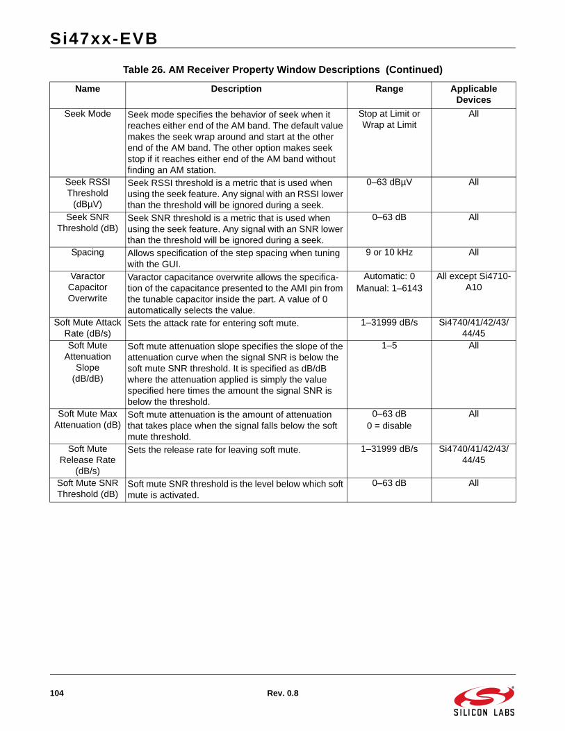
Si47xx-EVB
104 Rev. 0.8
Seek Mode Seek mode specifies the behavior of seek when it reaches either end of the AM band. The default value makes the seek wrap around and start at the other end of the AM band. The other option makes seek stop if it reaches either end of the AM band without finding an AM station.
Stop at Limit or Wrap at Limit
All
Seek RSSI Threshold
(dBµV)
Seek RSSI threshold is a metric that is used when using the seek feature. Any signal with an RSSI lower than the threshold will be ignored during a seek.
0–63 dBµV All
Seek SNR Threshold (dB)
Seek SNR threshold is a metric that is used when using the seek feature. Any signal with an SNR lower than the threshold will be ignored during a seek.
0–63 dB All
Spacing Allows specification of the step spacing when tuning with the GUI.
9 or 10 kHz All
Varactor Capacitor Overwrite
Varactor capacitance overwrite allows the specifica-tion of the capacitance presented to the AMI pin from the tunable capacitor inside the part. A value of 0 automatically selects the value.
Automatic: 0Manual: 1–6143
All except Si4710-A10
Soft Mute Attack Rate (dB/s)
Sets the attack rate for entering soft mute. 1–31999 dB/s Si4740/41/42/43/44/45
Soft Mute Attenuation
Slope (dB/dB)
Soft mute attenuation slope specifies the slope of the attenuation curve when the signal SNR is below the soft mute SNR threshold. It is specified as dB/dB where the attenuation applied is simply the value specified here times the amount the signal SNR is below the threshold.
1–5 All
Soft Mute Max Attenuation (dB)
Soft mute attenuation is the amount of attenuation that takes place when the signal falls below the soft mute threshold.
0–63 dB0 = disable
All
Soft Mute Release Rate
(dB/s)
Sets the release rate for leaving soft mute. 1–31999 dB/s Si4740/41/42/43/44/45
Soft Mute SNR Threshold (dB)
Soft mute SNR threshold is the level below which soft mute is activated.
0–63 dB All
Table 26. AM Receiver Property Window Descriptions (Continued)
Name Description Range Applicable Devices
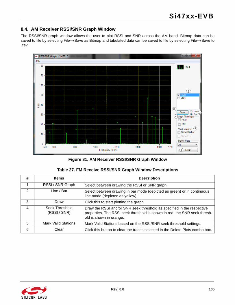
Si47xx-EVB
Rev. 0.8 105
8.4. AM Receiver RSSI/SNR Graph WindowThe RSSI/SNR graph window allows the user to plot RSSI and SNR across the AM band. Bitmap data can besaved to file by selecting FileSave as Bitmap and tabulated data can be saved to file by selecting FileSave to.csv.
Figure 81. AM Receiver RSSI/SNR Graph Window
Table 27. FM Receive RSSI/SNR Graph Window Descriptions
# Items Description
1 RSSI / SNR Graph Select between drawing the RSSI or SNR graph.
2 Line / Bar Select between drawing in bar mode (depicted as green) or in continuous line mode (depicted as yellow).
3 Draw Click this to start plotting the graph
4 Seek Threshold (RSSI / SNR)
Draw the RSSI and/or SNR seek threshold as specified in the respective properties. The RSSI seek threshold is shown in red; the SNR seek thresh-old is shown in orange.
5 Mark Valid Stations Mark Valid Stations based on the RSSI/SNR seek threshold settings.
6 Clear Click this button to clear the traces selected in the Delete Plots combo box.
1
2
3
4
5
6
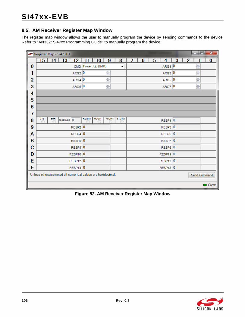
Si47xx-EVB
106 Rev. 0.8
8.5. AM Receiver Register Map WindowThe register map window allows the user to manually program the device by sending commands to the device.Refer to "AN332: Si47xx Programming Guide" to manually program the device.
Figure 82. AM Receiver Register Map Window
Si47xx-EVB
Rev. 0.8 107
8.6. AM Receiver Logging Tools Info8.6.1. Log Band Scan
Selecting ToolsLog Band Scan allows you to specify a filename and begin a scan of the entire band. The scanfeature starts with the first frequency in the band and then seeks to the first station that meets the seek criteria(Seek RSSI Threshold, Seek SNR Threshold). When a valid station is found, the software waits at the station andlogs Frequency, AFC, RSSI, SNR, Soft Mute etc settings and then seeks to the next valid station. While scanning,the software displays a green "Scanning" notice below the menu bar. The scan can be aborted by selecting theToolsLog Band Scan a second time. When the scan completes, the filename given is saved in comma separatedformat and is available for analysis in a text editor or spreadsheet.
8.6.2. Log Device Commands
Selecting ToolsLog Device Commands prompts for a filename in which all software API calls and data withtimestamp data will be logged as text. The logging will continue until ToolsLog Device Commands is selected asecond time, at which point the file is saved and available for analysis in a text editor.
8.6.3. Log Channel Info
Selecting ToolsLog Channel Info prompts for a filename in which all register values will be logged in commaseparated format. The software then logs all register values and the time at which it was received. The logging willcontinue until ToolsLog Channel Info is selected a second time, at which point the file is saved and available foranalysis in a text editor or spreadsheet.
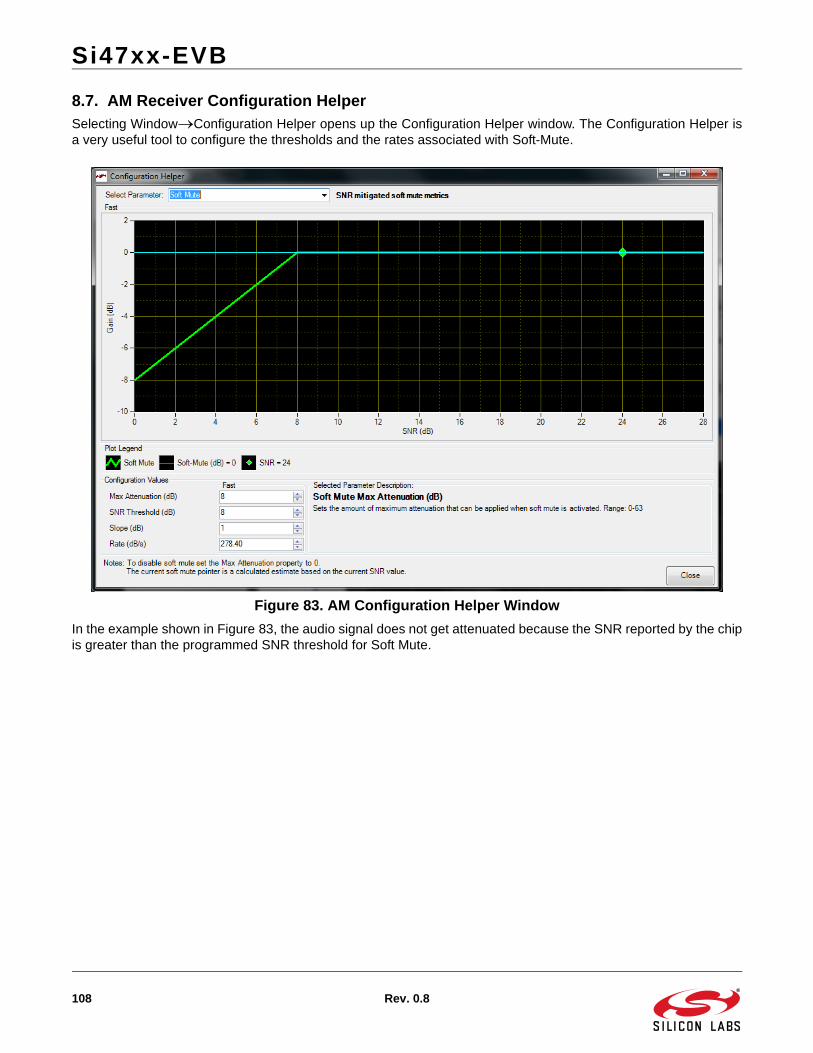
Si47xx-EVB
108 Rev. 0.8
8.7. AM Receiver Configuration HelperSelecting WindowConfiguration Helper opens up the Configuration Helper window. The Configuration Helper isa very useful tool to configure the thresholds and the rates associated with Soft-Mute.
Figure 83. AM Configuration Helper Window
In the example shown in Figure 83, the audio signal does not get attenuated because the SNR reported by the chipis greater than the programmed SNR threshold for Soft Mute.

Si47xx-EVB
Rev. 0.8 109
9. Using the EVB with a 9 V Battery
The EVB can be used with a 9 V battery that allows the user to disconnect the board from the computer forevaluating the Si47xx. Follow the guidelines listed below to use your EVB with a 9 V battery.
1. Put the switch SW1 in the Ext/Battery position.
2. Connect a 9 V battery to jumper J77.
3. Connect the USB cable.
4. Launch the GUI.
5. Initialize the EVB for AM or FM reception.
6. Once the desired station is tuned and all the settings for the receiver are according to the user's liking, please exit the GUI.
7. When asked whether to leave the device on, please click on yes.
8. Remove the USB cable.
9. The EVB can now be moved around.
Note that once the EVB is using its 9 V battery, it is not possible to change the tuned station. Repeat steps 3–9 totune the EVB to a different station while running on the 9 V battery.

Si47xx-EVB
110 Rev. 0.8
10. Debugging Guidelines for Si47xx EVB
Table 28. Debugging Guidelines for Si47xx EVB
Mode Symptom Solution
Configuration EVB not recognized If the EVB is not recognized by the PC, remove the USB connection and reconnect. Ensure the EVB is recognized by the PC by right-clicking on My Computer and selecting PropertiesHardwareDevice Manager. Under Human Interface Devices, select each HID-Compliant Device“Details entry and confirm one contains VID_10C4&PID_8244.
IF the EVB is not recognized by the GUI, but is recognized by the PC, it is likely that another process has erroneously acquired the handle to the EVB. Two processes known to cause this issue are lxhidsve.exe and EAUSBKBD.exe. Terminate these processes in the Task Manager.
If EVB is not recognized by the GUI, uninstall .NET framework 2.0 and reinstall from the installation CD or Microsoft’s website. The GUI requires .NET Framework 2.0; however, multiple versions such as 1.1, 2.0, and 3.0 may be installed simultaneously.
Initialization GUI crashes The GUI may crash if a previous GUI .ini file was not removed properly. Close the GUI, and delete all .ini files from the GUI directory. Launch the GUI and try again.
If the GUI continues to crash, close the GUI, remove the GUI from Control PanelAdd or Remove Programs, and then delete the GUI directory. Launch the GUI and try again.
Receive Audio clicking noise Disable "Update" under the "Control" menu (disables continuous GUI/Si47xx updates).
Receive Excess interference/Poor Reception
If using a laptop, ensure it is running off the battery and not plugged in to the ac mains.
Alternatively, disconnect from the host PC and run from battery power.
Move to a stronger signal environment.
Receive Seek/scan doesn’t find expected channels
Adjust Seek SNR and Seek RSSI thresholds downwards.
Verify band and channel spacing for the region.
Receive Seek/scan stops on noise
Adjust Seek SNR and Seek RSSI thresholds upwards.
If using a laptop, ensure it is running off the battery and not plugged in to the ac mains.
FM/WB Receive
Poor sensitivity from FM test port
Remove ac coupling cap from the headphone input path to eliminate possible sources of interference.
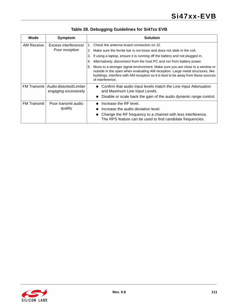
Si47xx-EVB
Rev. 0.8 111
AM Receive Excess interference/ Poor reception
1. Check the antenna board connection on J2.
2. Make sure the ferrite bar is not loose and does not slide in the coil.
3. If using a laptop, ensure it is running off the battery and not plugged in.
4. Alternatively, disconnect from the host PC and run from battery power.
5. Move to a stronger signal environment. Make sure you are close to a window or outside in the open when evaluating AM reception. Large metal structures, like buildings, interfere with AM reception so it is best to be away from these sources of interference.
FM Transmit Audio distorted/Limiter engaging excessively
Confirm that audio input levels match the Line Input Attenuation and Maximum Line Input Levels.
Disable or scale back the gain of the audio dynamic range control.
FM Transmit Poor transmit audio quality
Increase the RF level.
Increase the audio deviation level.
Change the RF frequency to a channel with less interference.The RPS feature can be used to find candidate frequencies.
Table 28. Debugging Guidelines for Si47xx EVB
Mode Symptom Solution
Si47xx-EVB
112 Rev. 0.8
11. Bill of Materials
Table 29. Si47xx-EVB Baseboard Rev 1.6 Bill of Materials
Item Qty RefDes Description Value Mfg/Vendor Mfg/Vendor_PN
1 1 J78 2.1 mm power plug CUI CONN_PJ-01
2 27 C1,C2,C4,C11,C13,C28,C31,C33,C34,C35,C36,C39,C40,C42,C43,C46,C50,C52,C54,C55,C57,
C61,C62,C68,C71,C73,C74
CAP,SM,0402,0.1UF,10% 0.1UF VENKEL C0402X7R160-104KNE
3 1 C72 RADIAL CAP 4.7UF Kemet T350B475K016AS
4 1 C70 CAP,SM,0805 0.1UF
5 1 C60 CAP,SM,7343,15UF,10% 15UF VISHAY 293D156X9020D2T
6 6 C18,C21,C22,C38,C69, C77
CAP,SM,0603,1UF,X7R 1UF VENKEL C0603X7R100-105KNE
7 2 C20,C41 CAP,SM,0402 24pf MURATA GRM1555C1H240JZ01D
8 5 C23,C26,C27,C30,C53 CAP,SM,0402,.01UF,10%,25V 0.01uF Kemet C0402C103K3RACTU
9 1 C59 CAP,SM,0402,22PF,10% 22Pf PANASONIC-ECG ECJ-0EC1H220J
10 8 C32,C37,C45,C47,C48,C49,C51,C65
CAP,SM,3216,16V 10UF VISHAY 293D106X9016A2
11 12 CAP,SM,0805 10UF MURATA GRM21BR71A106KE51L
12 3 C25,C3, C75 CAP,SM,0402,220PF,5% 220PF PANASONIC - ECG ECJ-0EC1H221J
13 1 C58 CAP,SM,3216,10V,10%,6.8UF 6.8UF EPCOS INC B45196H2685K109
14 1 C56 CAP,SM,0805,25V,10%,4.7UF 4.7UF MURATA GRM21BR61E475KA12L
15 2 C12,C76 CAP,SM,0402,820PF,5% 820pF MURATA GRM1555C1E821JA01
16 1 D1 LED,T-1 3/4.RED DIFFUSED LITEON LTL-10223W
17 2 FB1,FB2 FERRITE BEAD,SM STEWARD MI0805K400R-00
18 2 C100, C101 RES,SM,0805 0ohm VENKEL CR0805-16W-000T
19 3 J2,J17,J21 Solder jumpers
20 1 J77 CONN,TH,1X2,HDR SAMTEC TSW-102-07-G-S
21 5 J5,J13,J41,J61,J65 CONN,TH,1X3,HDR SAMTEC TSW-103-07-G-S
22 1 J62 CONN,TH,2X10,HDR SAMTEC TSW-110-07-G-D
23 1 J76 PCB TERMINAL BLOCK, 4 POSITION
MOUSER ELECTRONICS
651-1803293
24 2 J27,J75 CONN,TH,TFM,HDR,2X20,0.05X0.05IN PITCH
SAMTEC TFM-120-02-S-D-A
25 2 J24,J54 SMA_VERTICAL Digikey ARFX1231-ND
26 2 J32,J51 CONN,TH,1X8,HDR SAMTEC TSW-108-07-G-S
27 2 J68, J69 CONN,TH,1X3,HDR \ CONN,TH,1X1,HDR
SAMTEC TSW-103-07-G-S \ TSW-101-07-G-S
28 2 J6,J7 CONN,RCA,RIGHT ANGLE CUI RCJ-2123
29 1 J30 MINIJACK,3.3V,8MBPS SHARP GP1FD310TP
30 1 J19 MINIJACK,RCVR,3.3V,8MBPS SHARP GP1FD210RP
31 1 J74 HEADER,SHROUDED,5X2 3M 2510-6002UB
32 1 J79 CONN,TH,USB,RCPT,TYPE B 67068-0000 MOLEX/WALDOM ELECTRO
33 1 PB1 BUTTON,SM,LIGHT-TOUCH,160GF,6X3.5MM
PANASONIC - ECG EVQ-PPBA25
Note: SPDIF will not be supported on new EVBs as of February 14, 2011. On those boards items 29, 30, and 68—silkscreened as J30, J19 and U9—will not be populated.
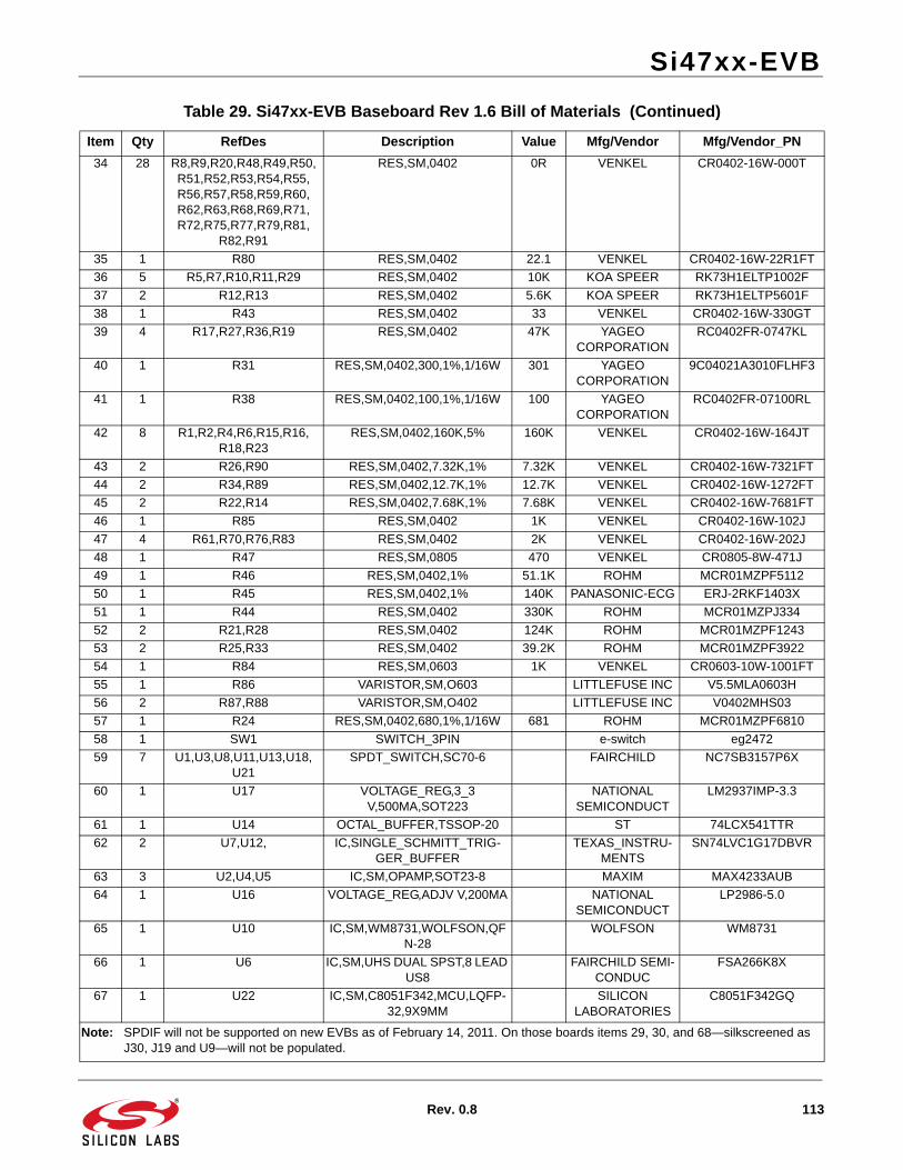
Si47xx-EVB
Rev. 0.8 113
34 28 R8,R9,R20,R48,R49,R50,R51,R52,R53,R54,R55,R56,R57,R58,R59,R60,R62,R63,R68,R69,R71,R72,R75,R77,R79,R81,
R82,R91
RES,SM,0402 0R VENKEL CR0402-16W-000T
35 1 R80 RES,SM,0402 22.1 VENKEL CR0402-16W-22R1FT
36 5 R5,R7,R10,R11,R29 RES,SM,0402 10K KOA SPEER RK73H1ELTP1002F
37 2 R12,R13 RES,SM,0402 5.6K KOA SPEER RK73H1ELTP5601F
38 1 R43 RES,SM,0402 33 VENKEL CR0402-16W-330GT
39 4 R17,R27,R36,R19 RES,SM,0402 47K YAGEO CORPORATION
RC0402FR-0747KL
40 1 R31 RES,SM,0402,300,1%,1/16W 301 YAGEO CORPORATION
9C04021A3010FLHF3
41 1 R38 RES,SM,0402,100,1%,1/16W 100 YAGEO CORPORATION
RC0402FR-07100RL
42 8 R1,R2,R4,R6,R15,R16,R18,R23
RES,SM,0402,160K,5% 160K VENKEL CR0402-16W-164JT
43 2 R26,R90 RES,SM,0402,7.32K,1% 7.32K VENKEL CR0402-16W-7321FT
44 2 R34,R89 RES,SM,0402,12.7K,1% 12.7K VENKEL CR0402-16W-1272FT
45 2 R22,R14 RES,SM,0402,7.68K,1% 7.68K VENKEL CR0402-16W-7681FT
46 1 R85 RES,SM,0402 1K VENKEL CR0402-16W-102J
47 4 R61,R70,R76,R83 RES,SM,0402 2K VENKEL CR0402-16W-202J
48 1 R47 RES,SM,0805 470 VENKEL CR0805-8W-471J
49 1 R46 RES,SM,0402,1% 51.1K ROHM MCR01MZPF5112
50 1 R45 RES,SM,0402,1% 140K PANASONIC-ECG ERJ-2RKF1403X
51 1 R44 RES,SM,0402 330K ROHM MCR01MZPJ334
52 2 R21,R28 RES,SM,0402 124K ROHM MCR01MZPF1243
53 2 R25,R33 RES,SM,0402 39.2K ROHM MCR01MZPF3922
54 1 R84 RES,SM,0603 1K VENKEL CR0603-10W-1001FT
55 1 R86 VARISTOR,SM,O603 LITTLEFUSE INC V5.5MLA0603H
56 2 R87,R88 VARISTOR,SM,O402 LITTLEFUSE INC V0402MHS03
57 1 R24 RES,SM,0402,680,1%,1/16W 681 ROHM MCR01MZPF6810
58 1 SW1 SWITCH_3PIN e-switch eg2472
59 7 U1,U3,U8,U11,U13,U18,U21
SPDT_SWITCH,SC70-6 FAIRCHILD NC7SB3157P6X
60 1 U17 VOLTAGE_REG,3_3 V,500MA,SOT223
NATIONAL SEMICONDUCT
LM2937IMP-3.3
61 1 U14 OCTAL_BUFFER,TSSOP-20 ST 74LCX541TTR
62 2 U7,U12, IC,SINGLE_SCHMITT_TRIG-GER_BUFFER
TEXAS_INSTRU-MENTS
SN74LVC1G17DBVR
63 3 U2,U4,U5 IC,SM,OPAMP,SOT23-8 MAXIM MAX4233AUB
64 1 U16 VOLTAGE_REG,ADJV V,200MA NATIONAL SEMICONDUCT
LP2986-5.0
65 1 U10 IC,SM,WM8731,WOLFSON,QFN-28
WOLFSON WM8731
66 1 U6 IC,SM,UHS DUAL SPST,8 LEAD US8
FAIRCHILD SEMI-CONDUC
FSA266K8X
67 1 U22 IC,SM,C8051F342,MCU,LQFP-32,9X9MM
SILICON LABORATORIES
C8051F342GQ
Table 29. Si47xx-EVB Baseboard Rev 1.6 Bill of Materials (Continued)
Item Qty RefDes Description Value Mfg/Vendor Mfg/Vendor_PN
Note: SPDIF will not be supported on new EVBs as of February 14, 2011. On those boards items 29, 30, and 68—silkscreened as J30, J19 and U9—will not be populated.
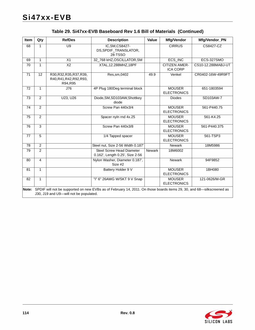
Si47xx-EVB
114 Rev. 0.8
68 1 U9 IC,SM,CS8427-DS,SPDIF_TRANSLATOR,
28-TSSO
CIRRUS CS8427-CZ
69 1 X1 32_768 kHZ,OSCILLATOR,SM ECS_INC ECS-327SMO
70 1 X2 XTAL,12.288MHZ,18PF CITIZEN AMER-ICA CORP
CS10-12.288MABJ-UT
71 12 R30,R32,R35,R37,R39,R40,R41,R42,R92,R93,
R94,R95
Res,sm,0402 49.9 Venkel CR0402-16W-49R9FT
72 1 J76 4P Plug 180Deg terminal block MOUSER ELECTRONICS
651-1803594
73 2 U23, U26 Diode,SM,SD103AW,Shottkey diode
Diodes SD103AW-7
74 2 Screw Pan 440x3/4 MOUSER ELECTRONICS
561-P440.75
75 2 Spacer nyln rnd 4x.25 MOUSER ELECTRONICS
561-K4.25
76 3 Screw Pan 440x3/8 MOUSER ELECTRONICS
561-P440.375
77 5 1/4 Tapped spacer MOUSER ELECTRONICS
561-TSP3
78 2 Steel nut, Size 2-56 Width 0.187' Newark 18M5986
79 2 Steel Screw Head Diameter 0.162', Length 0.25', Size 2-56
Newark 18M6002
80 4 Nylon Washer, Diameter 0.187', Size #2
Newark 94F9852
81 1 Battery Holder 9 V MOUSER ELECTRONICS
1BH080
82 1 "I" 6" 26AWG W/SKT 9 V Snap MOUSER ELECTRONICS
121-0626/M-GR
Table 29. Si47xx-EVB Baseboard Rev 1.6 Bill of Materials (Continued)
Item Qty RefDes Description Value Mfg/Vendor Mfg/Vendor_PN
Note: SPDIF will not be supported on new EVBs as of February 14, 2011. On those boards items 29, 30, and 68—silkscreened as J30, J19 and U9—will not be populated.
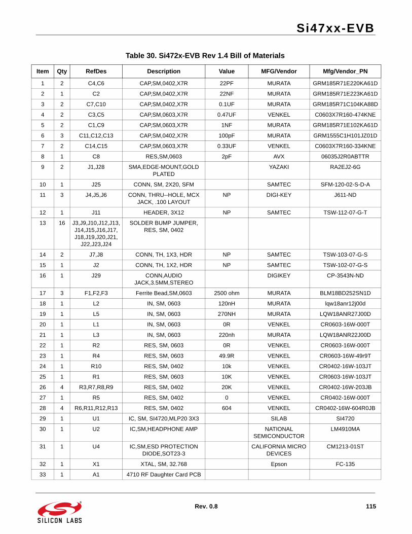
Si47xx-EVB
Rev. 0.8 115
Table 30. Si472x-EVB Rev 1.4 Bill of Materials
Item Qty RefDes Description Value MFG/Vendor Mfg/Vendor_PN
1 2 C4,C6 CAP,SM,0402,X7R 22PF MURATA GRM185R71E220KA61D
2 1 C2 CAP,SM,0402,X7R 22NF MURATA GRM185R71E223KA61D
3 2 C7,C10 CAP,SM,0402,X7R 0.1UF MURATA GRM185R71C104KA88D
4 2 C3,C5 CAP,SM,0603,X7R 0.47UF VENKEL C0603X7R160-474KNE
5 2 C1,C9 CAP,SM,0603,X7R 1NF MURATA GRM185R71E102KA61D
6 3 C11,C12,C13 CAP,SM,0402,X7R 100pF MURATA GRM1555C1H101JZ01D
7 2 C14,C15 CAP,SM,0603,X7R 0.33UF VENKEL C0603X7R160-334KNE
8 1 C8 RES,SM,0603 2pF AVX 06035J2R0ABTTR
9 2 J1,J28 SMA,EDGE-MOUNT,GOLD PLATED
YAZAKI RA2EJ2-6G
10 1 J25 CONN, SM, 2X20, SFM SAMTEC SFM-120-02-S-D-A
11 3 J4,J5,J6 CONN, THRU--HOLE, MCX JACK, .100 LAYOUT
NP DIGI-KEY J611-ND
12 1 J11 HEADER, 3X12 NP SAMTEC TSW-112-07-G-T
13 16 J3,J9,J10,J12,J13,J14,J15,J16,J17,J18,J19,J20,J21,
J22,J23,J24
SOLDER BUMP JUMPER, RES, SM, 0402
14 2 J7,J8 CONN, TH, 1X3, HDR NP SAMTEC TSW-103-07-G-S
15 1 J2 CONN, TH, 1X2, HDR NP SAMTEC TSW-102-07-G-S
16 1 J29 CONN,AUDIO JACK,3.5MM,STEREO
DIGIKEY CP-3543N-ND
17 3 F1,F2,F3 Ferrite Bead,SM,0603 2500 ohm MURATA BLM18BD252SN1D
18 1 L2 IN, SM, 0603 120nH MURATA lqw18anr12j00d
19 1 L5 IN, SM, 0603 270NH MURATA LQW18ANR27J00D
20 1 L1 IN, SM, 0603 0R VENKEL CR0603-16W-000T
21 1 L3 IN, SM, 0603 220nh MURATA LQW18ANR22J00D
22 1 R2 RES, SM, 0603 0R VENKEL CR0603-16W-000T
23 1 R4 RES, SM, 0603 49.9R VENKEL CR0603-16W-49r9T
24 1 R10 RES, SM, 0402 10k VENKEL CR0402-16W-103JT
25 1 R1 RES, SM, 0603 10K VENKEL CR0603-16W-103JT
26 4 R3,R7,R8,R9 RES, SM, 0402 20K VENKEL CR0402-16W-203JB
27 1 R5 RES, SM, 0402 0 VENKEL CR0402-16W-000T
28 4 R6,R11,R12,R13 RES, SM, 0402 604 VENKEL CR0402-16W-604R0JB
29 1 U1 IC, SM, SI4720,MLP20 3X3 SILAB SI4720
30 1 U2 IC,SM,HEADPHONE AMP NATIONAL SEMICONDUCTOR
LM4910MA
31 1 U4 IC,SM,ESD PROTECTION DIODE,SOT23-3
CALIFORNIA MICRO DEVICES
CM1213-01ST
32 1 X1 XTAL, SM, 32.768 Epson FC-135
33 1 A1 4710 RF Daughter Card PCB
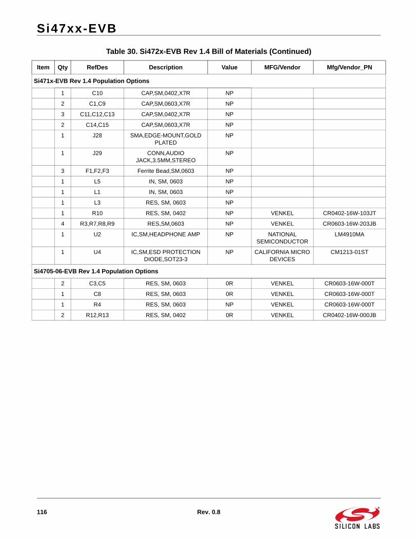
Si47xx-EVB
116 Rev. 0.8
Si471x-EVB Rev 1.4 Population Options
1 C10 CAP,SM,0402,X7R NP
2 C1,C9 CAP,SM,0603,X7R NP
3 C11,C12,C13 CAP,SM,0402,X7R NP
2 C14,C15 CAP,SM,0603,X7R NP
1 J28 SMA,EDGE-MOUNT,GOLD PLATED
NP
1 J29 CONN,AUDIO JACK,3.5MM,STEREO
NP
3 F1,F2,F3 Ferrite Bead,SM,0603 NP
1 L5 IN, SM, 0603 NP
1 L1 IN, SM, 0603 NP
1 L3 RES, SM, 0603 NP
1 R10 RES, SM, 0402 NP VENKEL CR0402-16W-103JT
4 R3,R7,R8,R9 RES,SM,0603 NP VENKEL CR0603-16W-203JB
1 U2 IC,SM,HEADPHONE AMP NP NATIONAL SEMICONDUCTOR
LM4910MA
1 U4 IC,SM,ESD PROTECTION DIODE,SOT23-3
NP CALIFORNIA MICRO DEVICES
CM1213-01ST
Si4705-06-EVB Rev 1.4 Population Options
2 C3,C5 RES, SM, 0603 0R VENKEL CR0603-16W-000T
1 C8 RES, SM, 0603 0R VENKEL CR0603-16W-000T
1 R4 RES, SM, 0603 NP VENKEL CR0603-16W-000T
2 R12,R13 RES, SM, 0402 0R VENKEL CR0402-16W-000JB
Table 30. Si472x-EVB Rev 1.4 Bill of Materials (Continued)
Item Qty RefDes Description Value MFG/Vendor Mfg/Vendor_PN
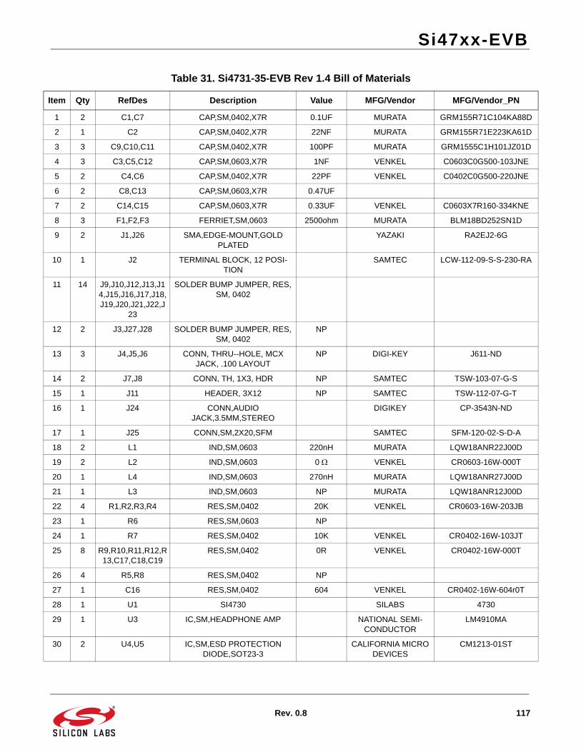
Si47xx-EVB
Rev. 0.8 117
Table 31. Si4731-35-EVB Rev 1.4 Bill of Materials
Item Qty RefDes Description Value MFG/Vendor MFG/Vendor_PN
1 2 C1,C7 CAP,SM,0402,X7R 0.1UF MURATA GRM155R71C104KA88D
2 1 C2 CAP,SM,0402,X7R 22NF MURATA GRM155R71E223KA61D
3 3 C9,C10,C11 CAP,SM,0402,X7R 100PF MURATA GRM1555C1H101JZ01D
4 3 C3,C5,C12 CAP,SM,0603,X7R 1NF VENKEL C0603C0G500-103JNE
5 2 C4,C6 CAP,SM,0402,X7R 22PF VENKEL C0402C0G500-220JNE
6 2 C8,C13 CAP,SM,0603,X7R 0.47UF
7 2 C14,C15 CAP,SM,0603,X7R 0.33UF VENKEL C0603X7R160-334KNE
8 3 F1,F2,F3 FERRIET,SM,0603 2500ohm MURATA BLM18BD252SN1D
9 2 J1,J26 SMA,EDGE-MOUNT,GOLD PLATED
YAZAKI RA2EJ2-6G
10 1 J2 TERMINAL BLOCK, 12 POSI-TION
SAMTEC LCW-112-09-S-S-230-RA
11 14 J9,J10,J12,J13,J14,J15,J16,J17,J18,J19,J20,J21,J22,J
23
SOLDER BUMP JUMPER, RES, SM, 0402
12 2 J3,J27,J28 SOLDER BUMP JUMPER, RES, SM, 0402
NP
13 3 J4,J5,J6 CONN, THRU--HOLE, MCX JACK, .100 LAYOUT
NP DIGI-KEY J611-ND
14 2 J7,J8 CONN, TH, 1X3, HDR NP SAMTEC TSW-103-07-G-S
15 1 J11 HEADER, 3X12 NP SAMTEC TSW-112-07-G-T
16 1 J24 CONN,AUDIO JACK,3.5MM,STEREO
DIGIKEY CP-3543N-ND
17 1 J25 CONN,SM,2X20,SFM SAMTEC SFM-120-02-S-D-A
18 2 L1 IND,SM,0603 220nH MURATA LQW18ANR22J00D
19 2 L2 IND,SM,0603 0 VENKEL CR0603-16W-000T
20 1 L4 IND,SM,0603 270nH MURATA LQW18ANR27J00D
21 1 L3 IND,SM,0603 NP MURATA LQW18ANR12J00D
22 4 R1,R2,R3,R4 RES,SM,0402 20K VENKEL CR0603-16W-203JB
23 1 R6 RES,SM,0603 NP
24 1 R7 RES,SM,0402 10K VENKEL CR0402-16W-103JT
25 8 R9,R10,R11,R12,R13,C17,C18,C19
RES,SM,0402 0R VENKEL CR0402-16W-000T
26 4 R5,R8 RES,SM,0402 NP
27 1 C16 RES,SM,0402 604 VENKEL CR0402-16W-604r0T
28 1 U1 SI4730 SILABS 4730
29 1 U3 IC,SM,HEADPHONE AMP NATIONAL SEMI-CONDUCTOR
LM4910MA
30 2 U4,U5 IC,SM,ESD PROTECTION DIODE,SOT23-3
CALIFORNIA MICRO DEVICES
CM1213-01ST
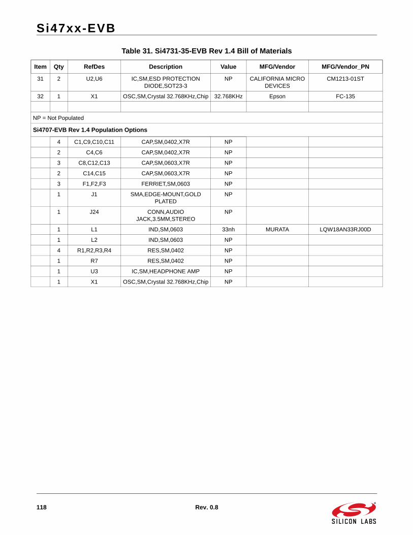
Si47xx-EVB
118 Rev. 0.8
31 2 U2,U6 IC,SM,ESD PROTECTION DIODE,SOT23-3
NP CALIFORNIA MICRO DEVICES
CM1213-01ST
32 1 X1 OSC,SM,Crystal 32.768KHz,Chip 32.768KHz Epson FC-135
NP = Not Populated
Si4707-EVB Rev 1.4 Population Options
4 C1,C9,C10,C11 CAP,SM,0402,X7R NP
2 C4,C6 CAP,SM,0402,X7R NP
3 C8,C12,C13 CAP,SM,0603,X7R NP
2 C14,C15 CAP,SM,0603,X7R NP
3 F1,F2,F3 FERRIET,SM,0603 NP
1 J1 SMA,EDGE-MOUNT,GOLD PLATED
NP
1 J24 CONN,AUDIO JACK,3.5MM,STEREO
NP
1 L1 IND,SM,0603 33nh MURATA LQW18AN33RJ00D
1 L2 IND,SM,0603 NP
4 R1,R2,R3,R4 RES,SM,0402 NP
1 R7 RES,SM,0402 NP
1 U3 IC,SM,HEADPHONE AMP NP
1 X1 OSC,SM,Crystal 32.768KHz,Chip NP
Table 31. Si4731-35-EVB Rev 1.4 Bill of Materials
Item Qty RefDes Description Value MFG/Vendor MFG/Vendor_PN
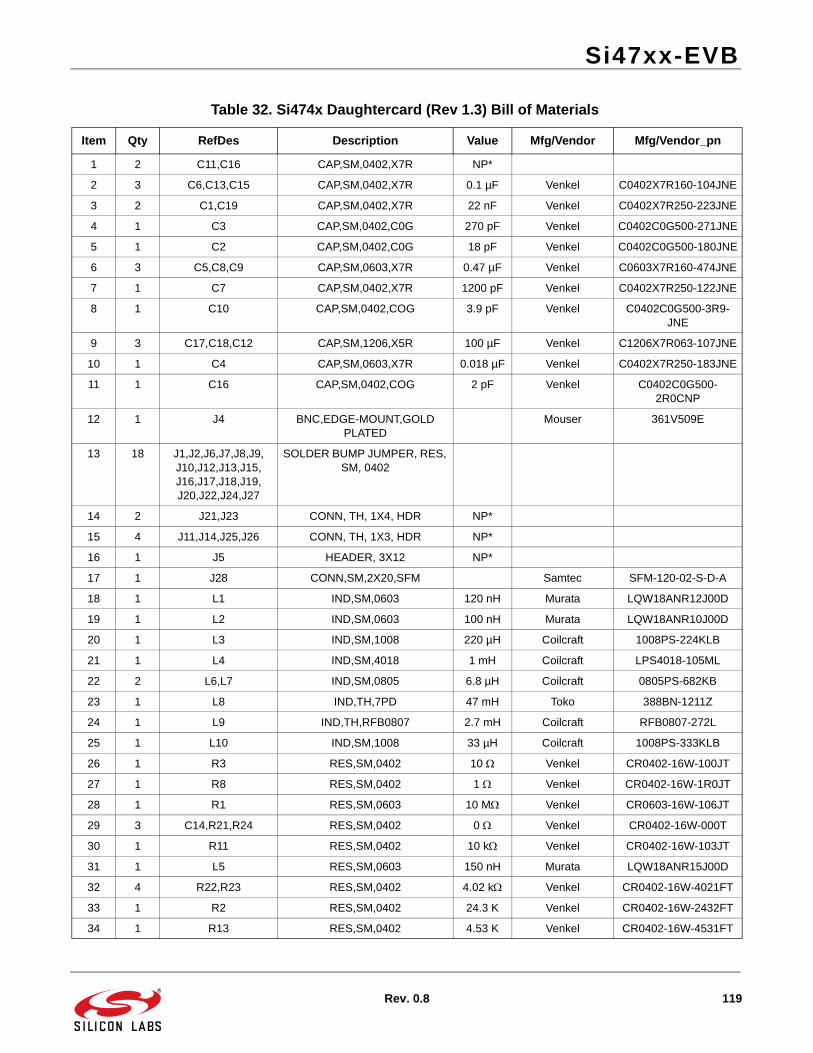
Si47xx-EVB
Rev. 0.8 119
Table 32. Si474x Daughtercard (Rev 1.3) Bill of Materials
Item Qty RefDes Description Value Mfg/Vendor Mfg/Vendor_pn
1 2 C11,C16 CAP,SM,0402,X7R NP*
2 3 C6,C13,C15 CAP,SM,0402,X7R 0.1 µF Venkel C0402X7R160-104JNE
3 2 C1,C19 CAP,SM,0402,X7R 22 nF Venkel C0402X7R250-223JNE
4 1 C3 CAP,SM,0402,C0G 270 pF Venkel C0402C0G500-271JNE
5 1 C2 CAP,SM,0402,C0G 18 pF Venkel C0402C0G500-180JNE
6 3 C5,C8,C9 CAP,SM,0603,X7R 0.47 µF Venkel C0603X7R160-474JNE
7 1 C7 CAP,SM,0402,X7R 1200 pF Venkel C0402X7R250-122JNE
8 1 C10 CAP,SM,0402,COG 3.9 pF Venkel C0402C0G500-3R9-JNE
9 3 C17,C18,C12 CAP,SM,1206,X5R 100 µF Venkel C1206X7R063-107JNE
10 1 C4 CAP,SM,0603,X7R 0.018 µF Venkel C0402X7R250-183JNE
11 1 C16 CAP,SM,0402,COG 2 pF Venkel C0402C0G500-2R0CNP
12 1 J4 BNC,EDGE-MOUNT,GOLD PLATED
Mouser 361V509E
13 18 J1,J2,J6,J7,J8,J9,J10,J12,J13,J15,J16,J17,J18,J19,J20,J22,J24,J27
SOLDER BUMP JUMPER, RES, SM, 0402
14 2 J21,J23 CONN, TH, 1X4, HDR NP*
15 4 J11,J14,J25,J26 CONN, TH, 1X3, HDR NP*
16 1 J5 HEADER, 3X12 NP*
17 1 J28 CONN,SM,2X20,SFM Samtec SFM-120-02-S-D-A
18 1 L1 IND,SM,0603 120 nH Murata LQW18ANR12J00D
19 1 L2 IND,SM,0603 100 nH Murata LQW18ANR10J00D
20 1 L3 IND,SM,1008 220 µH Coilcraft 1008PS-224KLB
21 1 L4 IND,SM,4018 1 mH Coilcraft LPS4018-105ML
22 2 L6,L7 IND,SM,0805 6.8 µH Coilcraft 0805PS-682KB
23 1 L8 IND,TH,7PD 47 mH Toko 388BN-1211Z
24 1 L9 IND,TH,RFB0807 2.7 mH Coilcraft RFB0807-272L
25 1 L10 IND,SM,1008 33 µH Coilcraft 1008PS-333KLB
26 1 R3 RES,SM,0402 10 Venkel CR0402-16W-100JT
27 1 R8 RES,SM,0402 1 Venkel CR0402-16W-1R0JT
28 1 R1 RES,SM,0603 10 M Venkel CR0603-16W-106JT
29 3 C14,R21,R24 RES,SM,0402 0 Venkel CR0402-16W-000T
30 1 R11 RES,SM,0402 10 k Venkel CR0402-16W-103JT
31 1 L5 RES,SM,0603 150 nH Murata LQW18ANR15J00D
32 4 R22,R23 RES,SM,0402 4.02 k Venkel CR0402-16W-4021FT
33 1 R2 RES,SM,0402 24.3 K Venkel CR0402-16W-2432FT
34 1 R13 RES,SM,0402 4.53 K Venkel CR0402-16W-4531FT
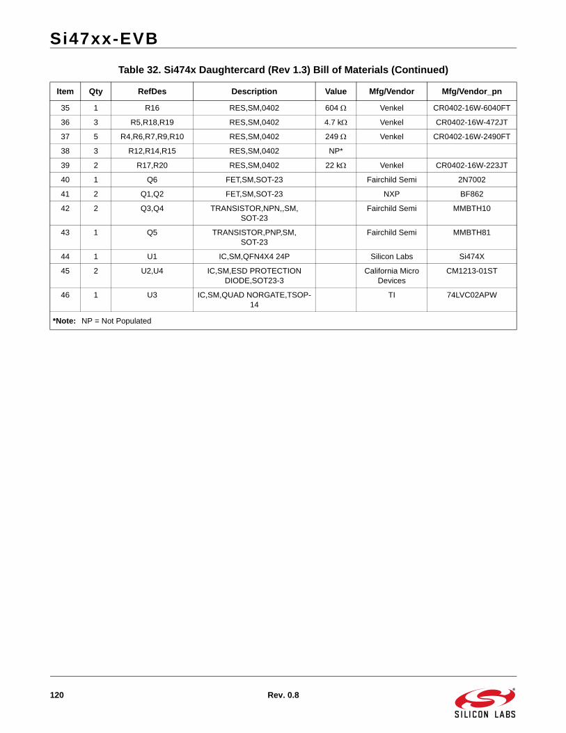
Si47xx-EVB
120 Rev. 0.8
35 1 R16 RES,SM,0402 604 Venkel CR0402-16W-6040FT
36 3 R5,R18,R19 RES,SM,0402 4.7 k Venkel CR0402-16W-472JT
37 5 R4,R6,R7,R9,R10 RES,SM,0402 249 Venkel CR0402-16W-2490FT
38 3 R12,R14,R15 RES,SM,0402 NP*
39 2 R17,R20 RES,SM,0402 22 k Venkel CR0402-16W-223JT
40 1 Q6 FET,SM,SOT-23 Fairchild Semi 2N7002
41 2 Q1,Q2 FET,SM,SOT-23 NXP BF862
42 2 Q3,Q4 TRANSISTOR,NPN,,SM,SOT-23
Fairchild Semi MMBTH10
43 1 Q5 TRANSISTOR,PNP,SM,SOT-23
Fairchild Semi MMBTH81
44 1 U1 IC,SM,QFN4X4 24P Silicon Labs Si474X
45 2 U2,U4 IC,SM,ESD PROTECTION DIODE,SOT23-3
California Micro Devices
CM1213-01ST
46 1 U3 IC,SM,QUAD NORGATE,TSOP-14
TI 74LVC02APW
*Note: NP = Not Populated
Table 32. Si474x Daughtercard (Rev 1.3) Bill of Materials (Continued)
Item Qty RefDes Description Value Mfg/Vendor Mfg/Vendor_pn
Si47xx-EVB
Rev. 0.8 121
Table 33. Si4749 Daughtercard (Rev 1.1) Bill of Materials
Item Qty RefDes Description Value Mfg/Vendor Mfg/Vendor_pn
1 3 C4,C6,C7 CAP,SM,0402,X7R 0.1 µF Venkel C0402X7R160-104JNE
2 1 C2 CAP,SM,0402,X7R 22 nF Venkel C0402X7R250-223JNE
3 2 C4,C6 CAP,SM,0402,C0G 24 pF Venkel C0402C0G500-240JNE
4 1 C1 CAP,SM,0402,C0G 100 pF Venkel C0402C0G500-101JNE
5 1 C8 CAP,SM,0402,X7R NP*
6 2 C3,C5 CAP,SM,0402,COG 0.01 µF Venkel C0402X7R250-103JNE
7 1 J1,J2 SMA,EDGE-MOUNT,GOLD PLATED
Yazaki RA2EJ2-6G
8 14 J9,J10,J12,J13,J14,J15,J16,J17,J18,J19,J
20,J21,J22,J23
SOLDER BUMP JUMPER, RES, SM, 0402
9 2 J27,J28 SOLDER BUMP JUMPER, RES, SM, 0402
NP*
10 3 J4,J5,J6 CONN, THRU--HOLE, MCX JACK, .100 LAYOUT
NP* Digi-Key J611-ND
11 2 J7,J8 CONN, TH, 1X3, HDR NP* SAMTEC TSW-103-07-G-S
12 1 J11 HEADER, 3X12 NP* SAMTEC TSW-112-07-G-T
13 1 J25 CONN,SM,2X20,SFM SAMTEC SFM-120-02-S-D-A
14 1 L1 IND,SM,0603 180 nH Murata LQW18ANR18J00D
15 1 L2 IND,SM,0603 NP
16 1 R1 RES,SM,0603 10 M Venkel CR0603-16W-106T
17 2 R2,R4 RES,SM,0402 64.9 Venkel CR0402-16W-64R9FT
18 6 R3,R7,R9 RES,SM,0402 0 Venkel CR0402-16W-000T
19 2 R6,R10 RES,SM,0402 2 k Venkel CR0402-16W-202T
20 1 R5 RES,SM,0402 604 Venkel CR0402-16W-604R0T
21 1 R9,.R11 RES,SM,0402 10 Venkel CR0402-16W-100JT
22 1 R8 RES,SM,0402 NP*
23 2 Q1,Q2 FET,SM,SOT-23 NXP BF862
24 1 U2 SI4749 Silicon Labs Si4749
25 1 U1 IC,SM,ESD PROTECTION DIODE,SOT23-3
California Micro Devices
CM1213-01ST
1 A1 PCB,Si4749EVB Silicon Labs
*Note: NP = Not Populated
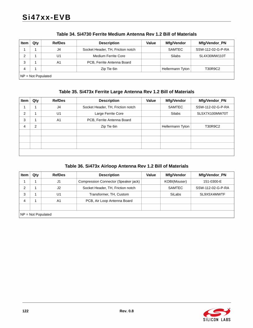
Si47xx-EVB
122 Rev. 0.8
Table 34. Si4730 Ferrite Medium Antenna Rev 1.2 Bill of Materials
Item Qty RefDes Description Value Mfg/Vendor Mfg/Vendor_PN
1 1 J4 Socket Header, TH, Friction notch SAMTEC SSW-112-02-G-P-RA
2 1 U1 Medium Ferrite Core Silabs SL4X30MW110T
3 1 A1 PCB, Ferrite Antenna Board
4 1 Zip Tie 6in Hellermann Tyton T30R9C2
NP = Not Populated
Table 35. Si473x Ferrite Large Antenna Rev 1.2 Bill of Materials
Item Qty RefDes Description Value Mfg/Vendor Mfg/Vendor_PN
1 1 J4 Socket Header, TH, Friction notch SAMTEC SSW-112-02-G-P-RA
2 1 U1 Large Ferrite Core Silabs SL5X7X100MW70T
3 1 A1 PCB, Ferrite Antenna Board
4 2 Zip Tie 6in Hellermann Tyton T30R9C2
Table 36. Si473x Airloop Antenna Rev 1.2 Bill of Materials
Item Qty RefDes Description Value Mfg/Vendor Mfg/Vendor_PN
1 1 J1 Compression Connector (Speaker jack) KOBI(Mouser) 151-0300-E
2 1 J2 Socket Header, TH, Friction notch SAMTEC SSW-112-02-G-P-RA
3 1 U1 Transformer, TH, Custom SiLabs SL9X5X4MWTF
4 1 A1 PCB, Air Loop Antenna Board
NP = Not Populated
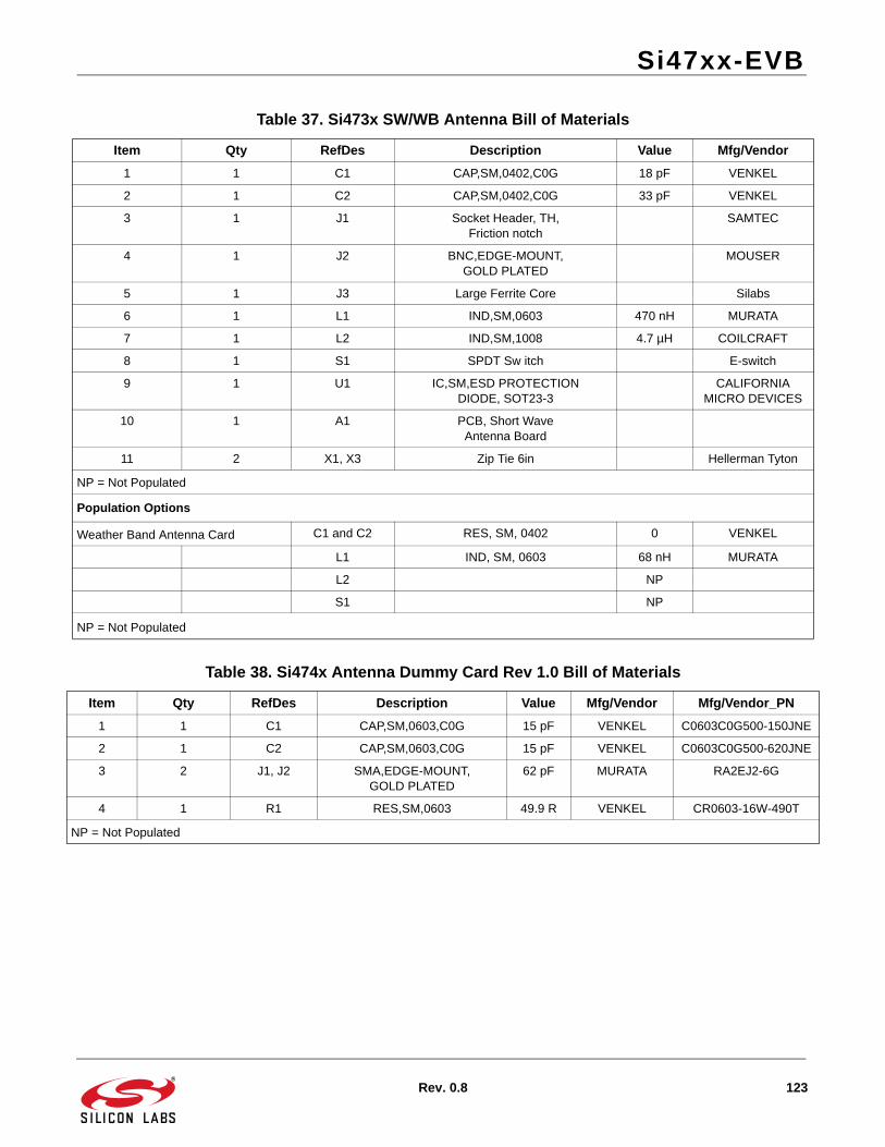
Si47xx-EVB
Rev. 0.8 123
Table 37. Si473x SW/WB Antenna Bill of Materials
Item Qty RefDes Description Value Mfg/Vendor
1 1 C1 CAP,SM,0402,C0G 18 pF VENKEL
2 1 C2 CAP,SM,0402,C0G 33 pF VENKEL
3 1 J1 Socket Header, TH,Friction notch
SAMTEC
4 1 J2 BNC,EDGE-MOUNT,GOLD PLATED
MOUSER
5 1 J3 Large Ferrite Core Silabs
6 1 L1 IND,SM,0603 470 nH MURATA
7 1 L2 IND,SM,1008 4.7 µH COILCRAFT
8 1 S1 SPDT Sw itch E-switch
9 1 U1 IC,SM,ESD PROTECTIONDIODE, SOT23-3
CALIFORNIA MICRO DEVICES
10 1 A1 PCB, Short WaveAntenna Board
11 2 X1, X3 Zip Tie 6in Hellerman Tyton
NP = Not Populated
Population Options
Weather Band Antenna Card C1 and C2 RES, SM, 0402 0 VENKEL
L1 IND, SM, 0603 68 nH MURATA
L2 NP
S1 NP
NP = Not Populated
Table 38. Si474x Antenna Dummy Card Rev 1.0 Bill of Materials
Item Qty RefDes Description Value Mfg/Vendor Mfg/Vendor_PN
1 1 C1 CAP,SM,0603,C0G 15 pF VENKEL C0603C0G500-150JNE
2 1 C2 CAP,SM,0603,C0G 15 pF VENKEL C0603C0G500-620JNE
3 2 J1, J2 SMA,EDGE-MOUNT,GOLD PLATED
62 pF MURATA RA2EJ2-6G
4 1 R1 RES,SM,0603 49.9 R VENKEL CR0603-16W-490T
NP = Not Populated
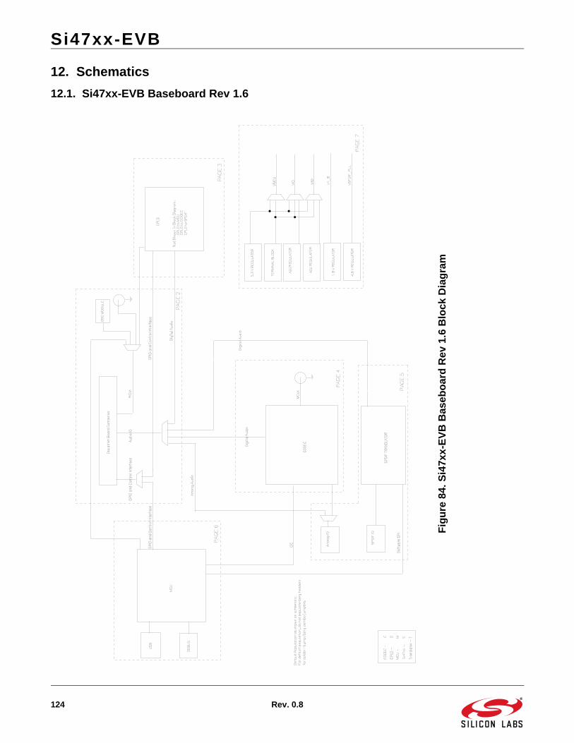
Si47xx-EVB
124 Rev. 0.8
12. Schematics
12.1. Si47xx-EVB Baseboard Rev 1.6
Fig
ure
84.S
i47x
x-E
VB
Bas
ebo
ard
Rev
1.6
Blo
ck D
iag
ram
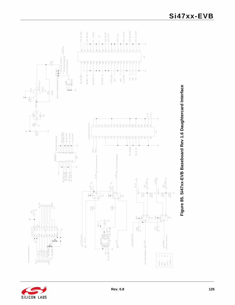
Si47xx-EVB
Rev. 0.8 125
Fig
ure
85.S
i47x
x-E
VB
Bas
ebo
ard
Rev
1.6
Dau
gh
terc
ard
Inte
rfac
e
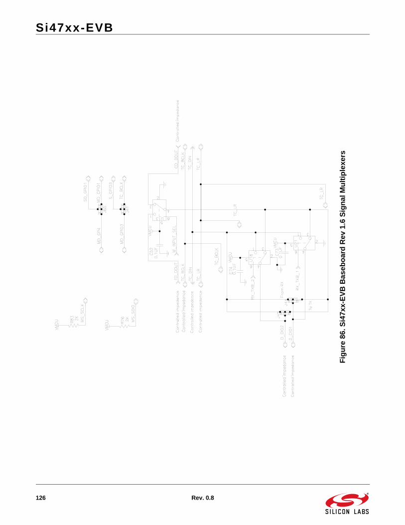
Si47xx-EVB
126 Rev. 0.8
Fig
ure
86.S
i47x
x-E
VB
Bas
ebo
ard
Rev
1.6
Sig
nal
Mu
ltip
lexe
rs
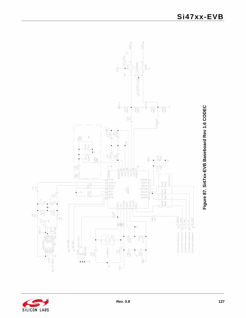
Si47xx-EVB
Rev. 0.8 127
Fig
ure
87.S
i47x
x-E
VB
Bas
ebo
ard
Rev
1.6
CO
DE
C
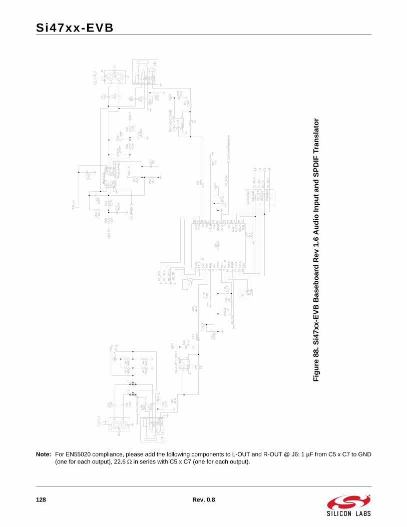
Si47xx-EVB
128 Rev. 0.8
Note: For EN55020 compliance, please add the following components to L-OUT and R-OUT @ J6: 1 µF from C5 x C7 to GND(one for each output), 22.6 in series with C5 x C7 (one for each output).
Fig
ure
88.S
i47x
x-E
VB
Bas
ebo
ard
Rev
1.6
Au
dio
Inp
ut
and
SP
DIF
Tra
nsl
ato
r
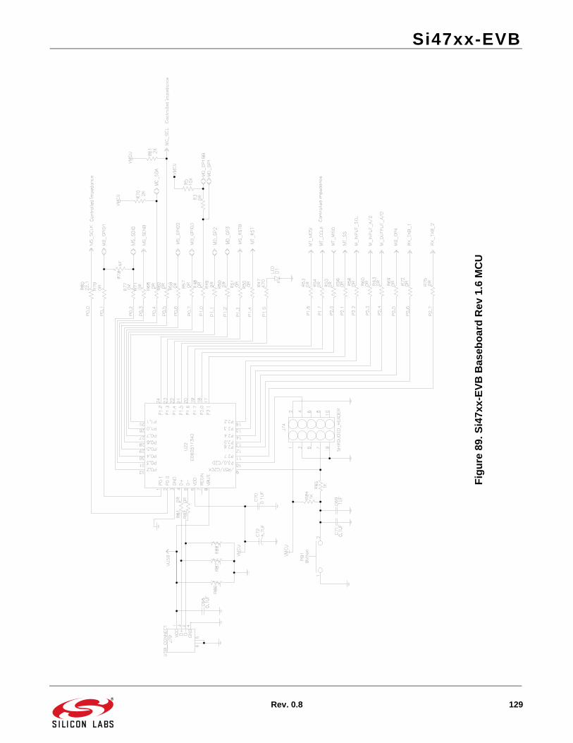
Si47xx-EVB
Rev. 0.8 129
Fig
ure
89.S
i47x
x-E
VB
Bas
ebo
ard
Rev
1.6
MC
U
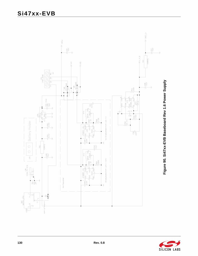
Si47xx-EVB
130 Rev. 0.8
Fig
ure
90.S
i47x
x-E
VB
Bas
ebo
ard
Rev
1.6
Po
wer
Su
pp
ly
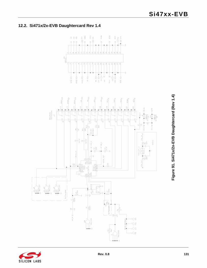
Si47xx-EVB
Rev. 0.8 131
12.2. Si471x/2x-EVB Daughtercard Rev 1.4
Fig
ure
91.S
i471
x/2x
-EV
B D
aug
hte
rcar
d (
Rev
1.4
)
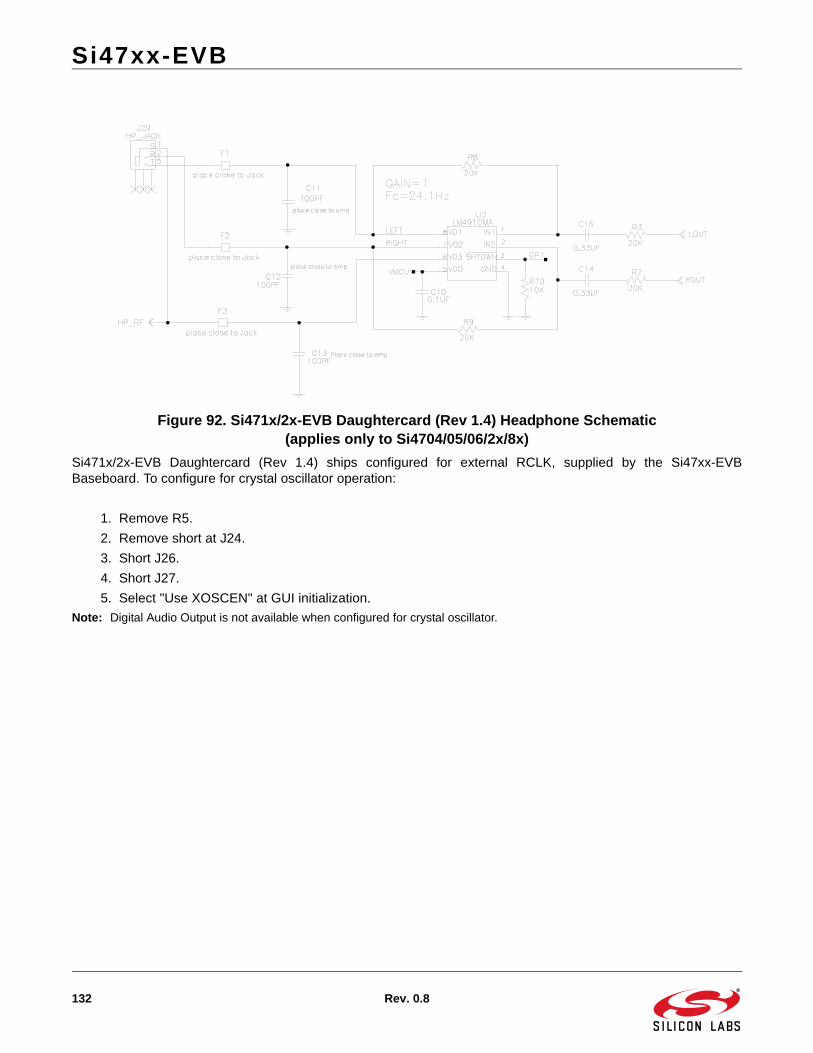
Si47xx-EVB
132 Rev. 0.8
Figure 92. Si471x/2x-EVB Daughtercard (Rev 1.4) Headphone Schematic (applies only to Si4704/05/06/2x/8x)
Si471x/2x-EVB Daughtercard (Rev 1.4) ships configured for external RCLK, supplied by the Si47xx-EVBBaseboard. To configure for crystal oscillator operation:
1. Remove R5.
2. Remove short at J24.
3. Short J26.
4. Short J27.
5. Select "Use XOSCEN" at GUI initialization.
Note: Digital Audio Output is not available when configured for crystal oscillator.
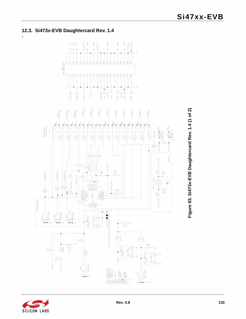
Si47xx-EVB
Rev. 0.8 133
12.3. Si473x-EVB Daughtercard Rev. 1.47
Fig
ure
93.S
i473
x-E
VB
Dau
gh
terc
ard
Rev
. 1.4
(1
of
2)
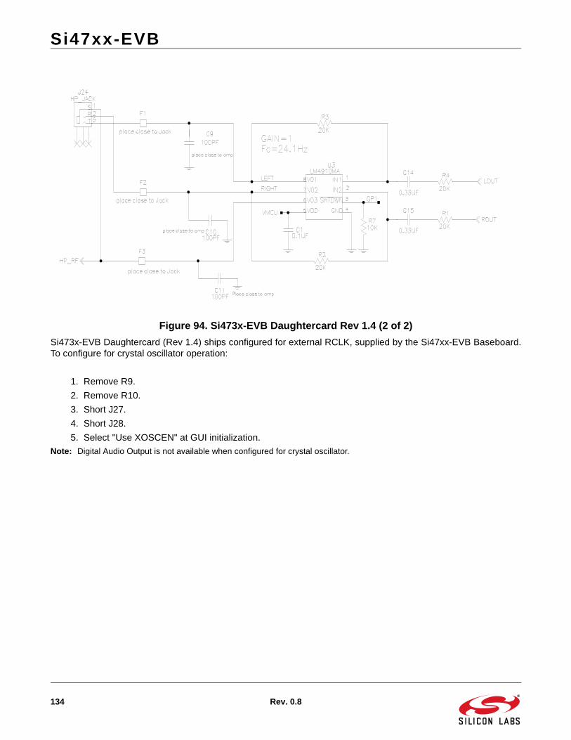
Si47xx-EVB
134 Rev. 0.8
Figure 94. Si473x-EVB Daughtercard Rev 1.4 (2 of 2)
Si473x-EVB Daughtercard (Rev 1.4) ships configured for external RCLK, supplied by the Si47xx-EVB Baseboard.To configure for crystal oscillator operation:
1. Remove R9.
2. Remove R10.
3. Short J27.
4. Short J28.
5. Select "Use XOSCEN" at GUI initialization.
Note: Digital Audio Output is not available when configured for crystal oscillator.
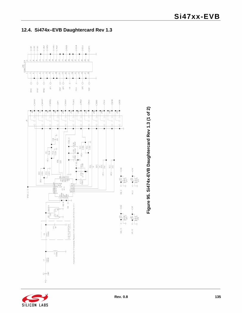
Si47xx-EVB
Rev. 0.8 135
12.4. Si474x–EVB Daughtercard Rev 1.3
Fig
ure
95.S
i474
x-E
VB
Dau
gh
terc
ard
Rev
1.3
(1
of
2)
Si47xx-EVB
136 Rev. 0.8
Fig
ure
96.S
i474
x-E
VB
Dau
gh
terc
ard
Rev
1.3
(2
of
2)
Si47xx-EVB
Rev. 0.8 137
12.5. Si4749-EVB Daughtercard Rev 1.1
Fig
ure
97.S
i474
9-E
VB
Dau
gh
terc
ard
Rev
1.1
(1
of
2)
Si47xx-EVB
138 Rev. 0.8
Figure 98. Si4749-EVB Daughtercard Rev 1.1 (2 of 2)
Note: C4, C6, R9, and R11 manually added to Si4749EVB Rev 1.0 to create Si4749EVB Rev 1.1.
Si47xx-EVB
Rev. 0.8 139
12.6. Antenna Card Schematics12.6.1. Si473x Ferrite Antenna Card Rev 1.2
Figure 99. Ferrite Antenna Card Rev 1.2
12.6.2. Si473x Air Loop Antenna Card Rev 1.2
Figure 100. Airloop Antenna Card Rev 1.2
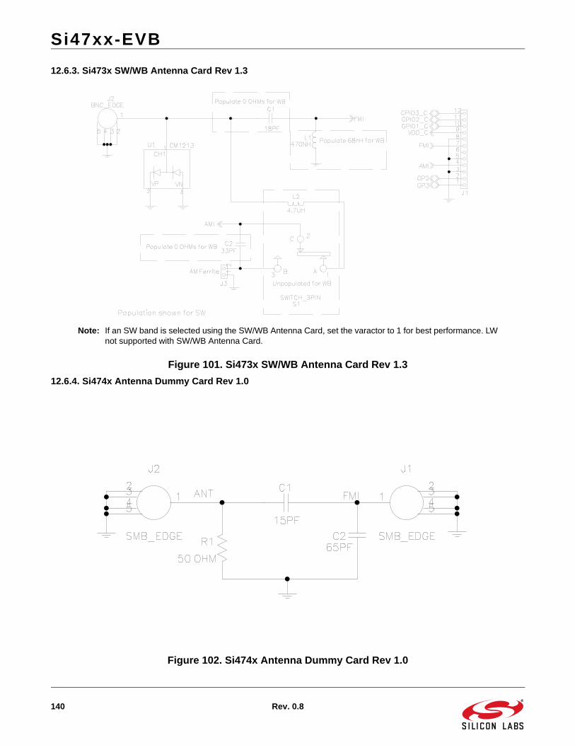
Si47xx-EVB
140 Rev. 0.8
12.6.3. Si473x SW/WB Antenna Card Rev 1.3
Figure 101. Si473x SW/WB Antenna Card Rev 1.3
12.6.4. Si474x Antenna Dummy Card Rev 1.0
Figure 102. Si474x Antenna Dummy Card Rev 1.0
Note: If an SW band is selected using the SW/WB Antenna Card, set the varactor to 1 for best performance. LWnot supported with SW/WB Antenna Card.
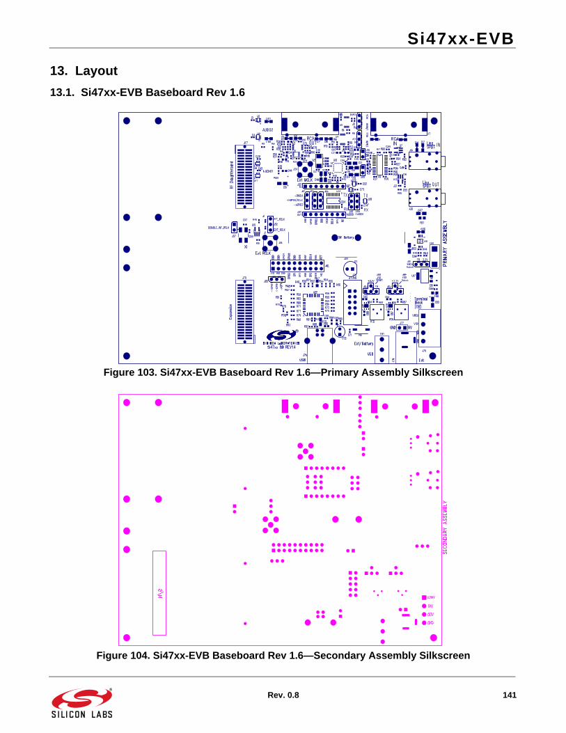
Si47xx-EVB
Rev. 0.8 141
13. Layout
13.1. Si47xx-EVB Baseboard Rev 1.6
Figure 103. Si47xx-EVB Baseboard Rev 1.6—Primary Assembly Silkscreen
Figure 104. Si47xx-EVB Baseboard Rev 1.6—Secondary Assembly Silkscreen
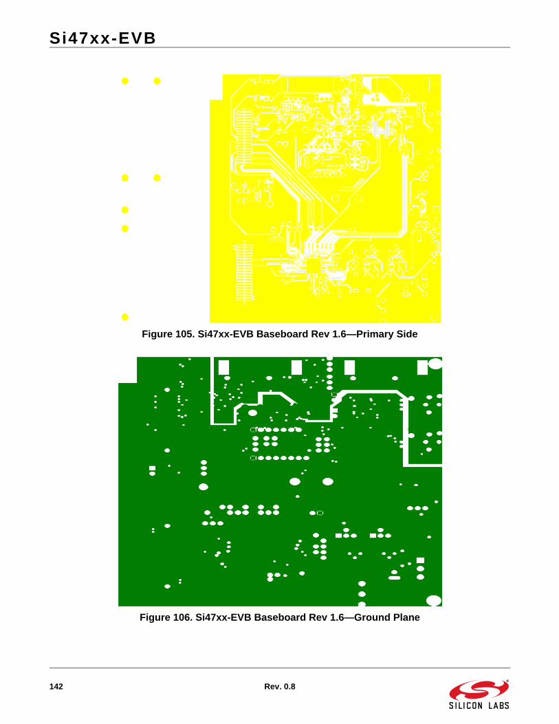
Si47xx-EVB
142 Rev. 0.8
Figure 105. Si47xx-EVB Baseboard Rev 1.6—Primary Side
Figure 106. Si47xx-EVB Baseboard Rev 1.6—Ground Plane
Si47xx-EVB
Rev. 0.8 143
Figure 107. Si47xx-EVB Baseboard Rev 1.6—Power Plane
Figure 108. Si47xx-EVB Baseboard Rev 1.6—Secondary Side
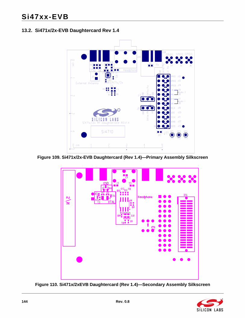
Si47xx-EVB
144 Rev. 0.8
13.2. Si471x/2x-EVB Daughtercard Rev 1.4
Figure 109. Si471x/2x-EVB Daughtercard (Rev 1.4)—Primary Assembly Silkscreen
Figure 110. Si471x/2xEVB Daughtercard (Rev 1.4)—Secondary Assembly Silkscreen
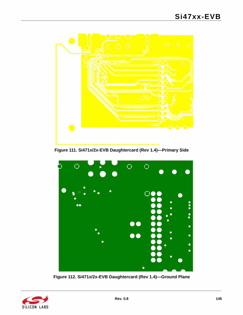
Si47xx-EVB
Rev. 0.8 145
Figure 111. Si471x/2x-EVB Daughtercard (Rev 1.4)—Primary Side
Figure 112. Si471x/2x-EVB Daughtercard (Rev 1.4)—Ground Plane
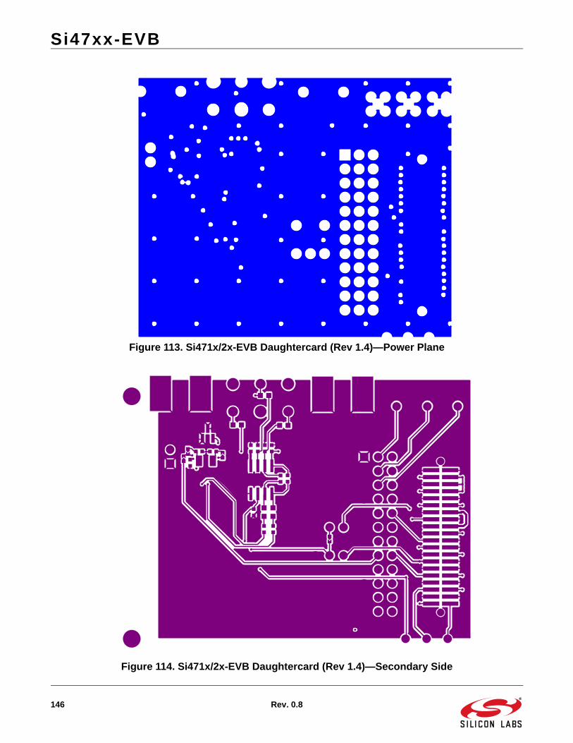
Si47xx-EVB
146 Rev. 0.8
Figure 113. Si471x/2x-EVB Daughtercard (Rev 1.4)—Power Plane
Figure 114. Si471x/2x-EVB Daughtercard (Rev 1.4)—Secondary Side

Si47xx-EVB
Rev. 0.8 147
13.3. Si473x-EVB Daughtercard Rev 1.4
Figure 115. Si473x-EVB Daughtercard Rev 1.4 - Primary Assembly Silkscreen
Figure 116. Si473x-EVB Daughtercard Rev 1.4 - Secondary Assembly Silkscreen
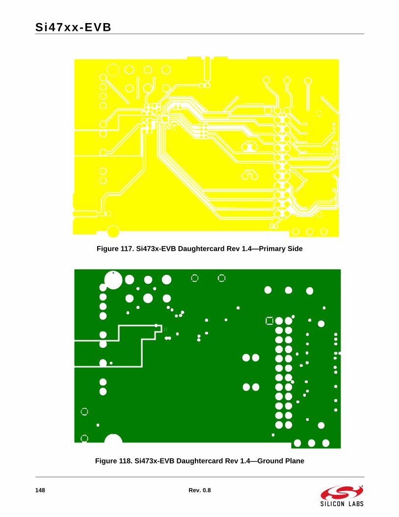
Si47xx-EVB
148 Rev. 0.8
Figure 117. Si473x-EVB Daughtercard Rev 1.4—Primary Side
Figure 118. Si473x-EVB Daughtercard Rev 1.4—Ground Plane
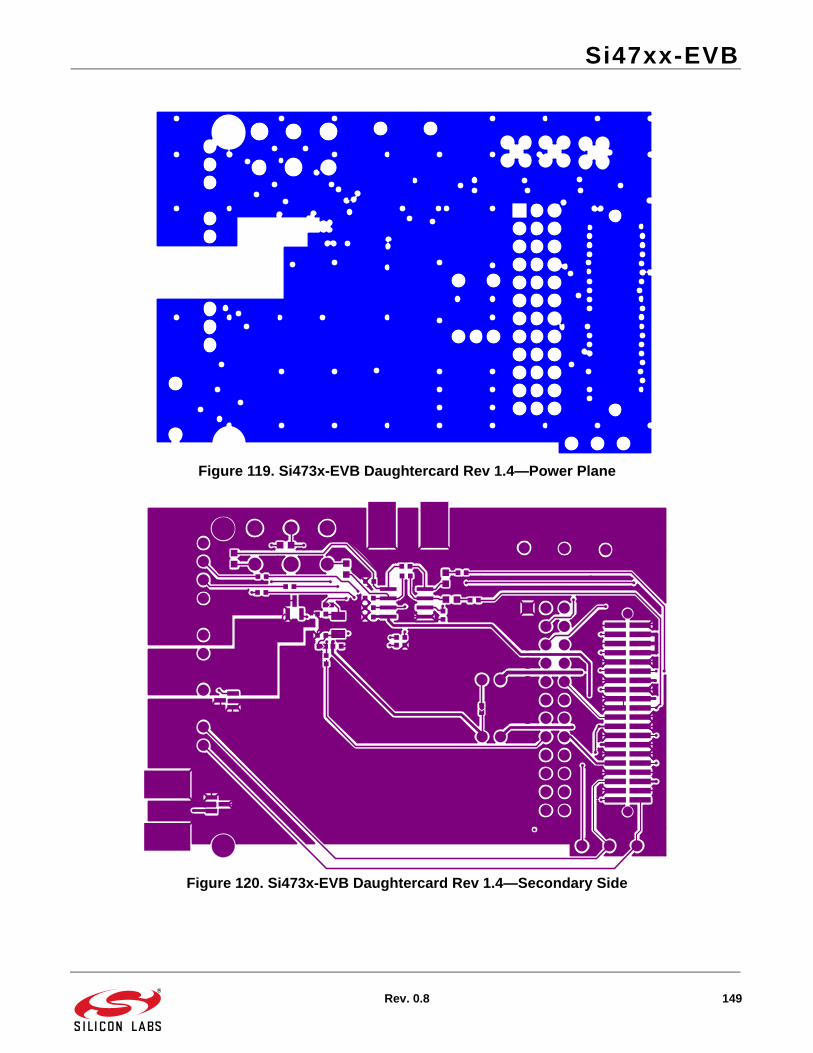
Si47xx-EVB
Rev. 0.8 149
Figure 119. Si473x-EVB Daughtercard Rev 1.4—Power Plane
Figure 120. Si473x-EVB Daughtercard Rev 1.4—Secondary Side
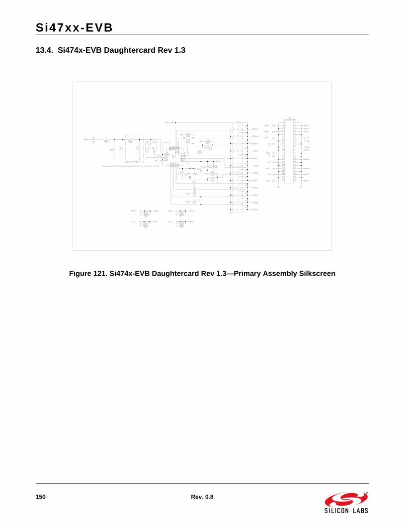
Si47xx-EVB
150 Rev. 0.8
13.4. Si474x-EVB Daughtercard Rev 1.3
Figure 121. Si474x-EVB Daughtercard Rev 1.3—Primary Assembly Silkscreen
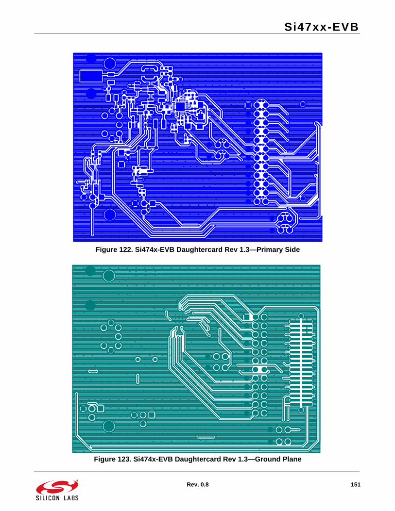
Si47xx-EVB
Rev. 0.8 151
Figure 122. Si474x-EVB Daughtercard Rev 1.3—Primary Side
Figure 123. Si474x-EVB Daughtercard Rev 1.3—Ground Plane
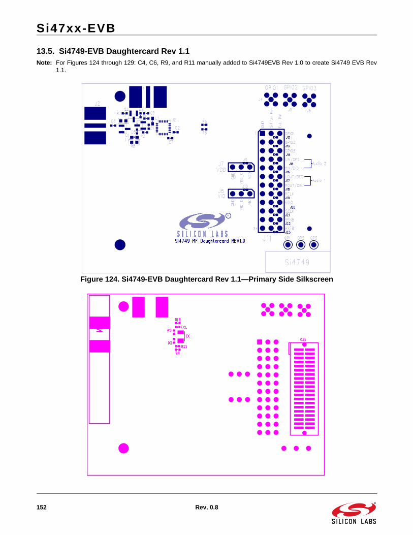
Si47xx-EVB
152 Rev. 0.8
13.5. Si4749-EVB Daughtercard Rev 1.1Note: For Figures 124 through 129: C4, C6, R9, and R11 manually added to Si4749EVB Rev 1.0 to create Si4749 EVB Rev
1.1.
Figure 124. Si4749-EVB Daughtercard Rev 1.1—Primary Side Silkscreen
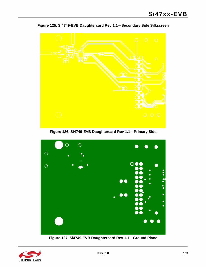
Si47xx-EVB
Rev. 0.8 153
Figure 125. Si4749-EVB Daughtercard Rev 1.1—Secondary Side Silkscreen
Figure 126. Si4749-EVB Daughtercard Rev 1.1—Primary Side
Figure 127. Si4749-EVB Daughtercard Rev 1.1—Ground Plane
Si47xx-EVB
154 Rev. 0.8
Figure 128. Si4749-EVB Daughtercard Rev 1.1—Power Plane
Figure 129. Si4749-EVB Daughtercard Rev 1.1—Secondary Side
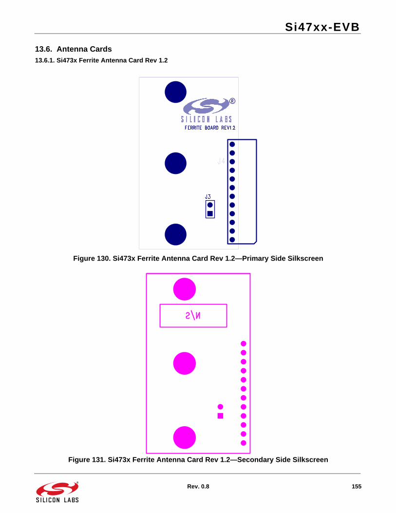
Si47xx-EVB
Rev. 0.8 155
13.6. Antenna Cards13.6.1. Si473x Ferrite Antenna Card Rev 1.2
Figure 130. Si473x Ferrite Antenna Card Rev 1.2—Primary Side Silkscreen
Figure 131. Si473x Ferrite Antenna Card Rev 1.2—Secondary Side Silkscreen
Si47xx-EVB
156 Rev. 0.8
Figure 132. Si473x Ferrite Antenna Card Rev 1.2—Primary Side
Figure 133. Si473x Ferrite Antenna Card Rev 1.2—Secondary Side
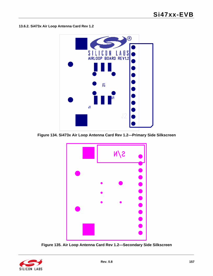
Si47xx-EVB
Rev. 0.8 157
13.6.2. Si473x Air Loop Antenna Card Rev 1.2
Figure 134. Si473x Air Loop Antenna Card Rev 1.2—Primary Side Silkscreen
Figure 135. Air Loop Antenna Card Rev 1.2—Secondary Side Silkscreen
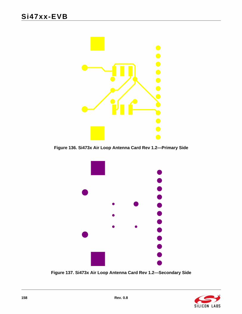
Si47xx-EVB
158 Rev. 0.8
Figure 136. Si473x Air Loop Antenna Card Rev 1.2—Primary Side
Figure 137. Si473x Air Loop Antenna Card Rev 1.2—Secondary Side
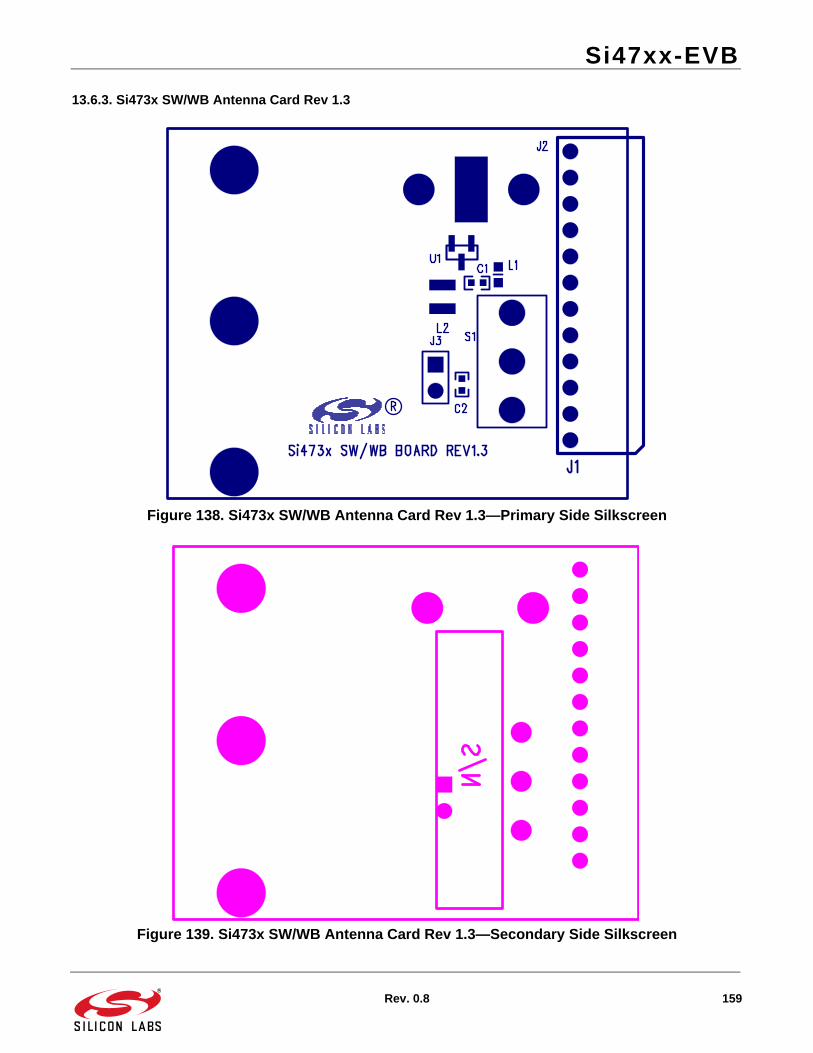
Si47xx-EVB
Rev. 0.8 159
13.6.3. Si473x SW/WB Antenna Card Rev 1.3
Figure 138. Si473x SW/WB Antenna Card Rev 1.3—Primary Side Silkscreen
Figure 139. Si473x SW/WB Antenna Card Rev 1.3—Secondary Side Silkscreen
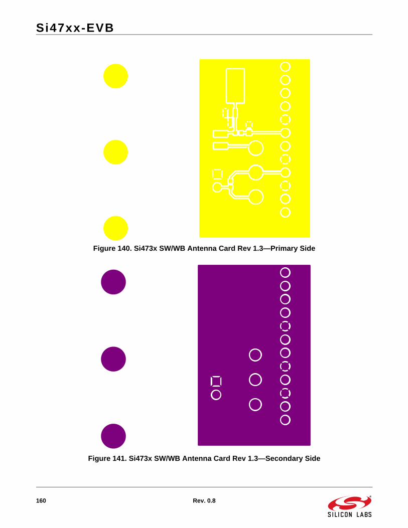
Si47xx-EVB
160 Rev. 0.8
Figure 140. Si473x SW/WB Antenna Card Rev 1.3—Primary Side
Figure 141. Si473x SW/WB Antenna Card Rev 1.3—Secondary Side
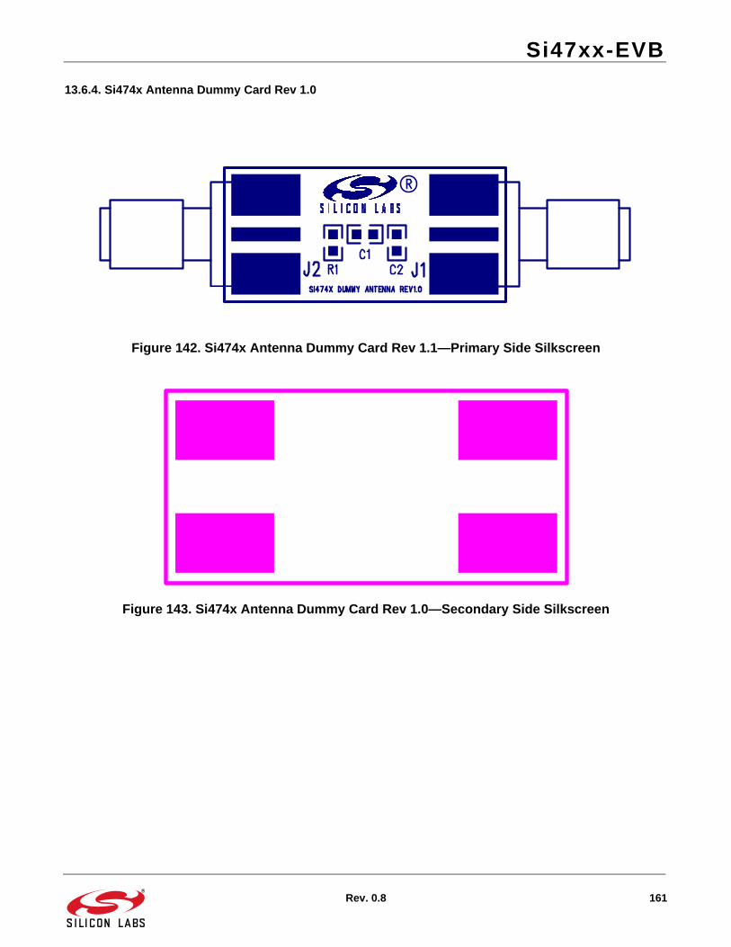
Si47xx-EVB
Rev. 0.8 161
13.6.4. Si474x Antenna Dummy Card Rev 1.0
Figure 142. Si474x Antenna Dummy Card Rev 1.1—Primary Side Silkscreen
Figure 143. Si474x Antenna Dummy Card Rev 1.0—Secondary Side Silkscreen
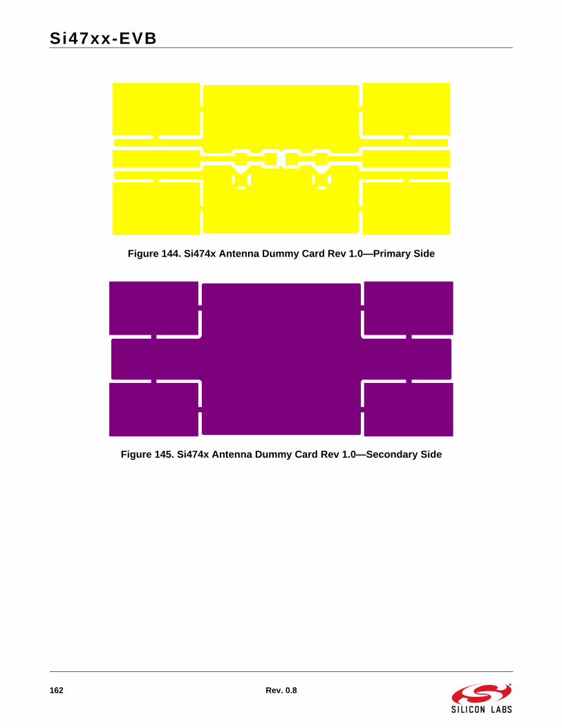
Si47xx-EVB
162 Rev. 0.8
Figure 144. Si474x Antenna Dummy Card Rev 1.0—Primary Side
Figure 145. Si474x Antenna Dummy Card Rev 1.0—Secondary Side
Si47xx-EVB
Rev. 0.8 163
DOCUMENTATION CHANGE LIST
Revision 0.1 to Revision 0.2 Updated Product Family in Table 1 on page 1.
Updated Si4740/41 Property List in Figure on page 67 and Table 15 on page 67.
Clarified varactor recommendation with SW operation using SW/WB Antenna Card.
Added instructions for daughtercard configurations with crystal oscillator operation.
Added Si4707 and SAME support to Section 7.
Revision 0.2 to Revision 0.3 Added Si4742/43 support.
Revision 0.3 to Revision 0.4 Removed Si4706, Si4707, and Si474x NDA
information from document.
Revision 0.4 to Revision 0.5 Updated for new 4.0 GUI version
Updated EVB BOM and Schematics to 1.6
Revision 0.5 to Revision 0.6 Added information on State Management
Updated figures to represent Silicon Labs Audio GUI version 07.2.0
Revision 0.6 to Revision 0.7 Added Si4706/07/4x-EVB information
Revision 0.7 to Revision 0.8 Updated for GUI version 8.2.13

DisclaimerSilicon Laboratories intends to provide customers with the latest, accurate, and in-depth documentation of all peripherals and modules available for system and software implementers using or intending to use the Silicon Laboratories products. Characterization data, available modules and peripherals, memory sizes and memory addresses refer to each specific device, and "Typical" parameters provided can and do vary in different applications. Application examples described herein are for illustrative purposes only. Silicon Laboratories reserves the right to make changes without further notice and limitation to product information, specifications, and descriptions herein, and does not give warranties as to the accuracy or completeness of the included information. Silicon Laboratories shall have no liability for the consequences of use of the information supplied herein. This document does not imply or express copyright licenses granted hereunder to design or fabricate any integrated circuits. The products must not be used within any Life Support System without the specific written consent of Silicon Laboratories. A "Life Support System" is any product or system intended to support or sustain life and/or health, which, if it fails, can be reasonably expected to result in significant personal injury or death. Silicon Laboratories products are generally not intended for military applications. Silicon Laboratories products shall under no circumstances be used in weapons of mass destruction including (but not limited to) nuclear, biological or chemical weapons, or missiles capable of delivering such weapons.
Trademark InformationSilicon Laboratories Inc., Silicon Laboratories, Silicon Labs, SiLabs and the Silicon Labs logo, CMEMS®, EFM, EFM32, EFR, Energy Micro, Energy Micro logo and combinations thereof, "the world’s most energy friendly microcontrollers", Ember®, EZLink®, EZMac®, EZRadio®, EZRadioPRO®, DSPLL®, ISOmodem ®, Precision32®, ProSLIC®, SiPHY®, USBXpress® and others are trademarks or registered trademarks of Silicon Laboratories Inc. ARM, CORTEX, Cortex-M3 and THUMB are trademarks or registered trademarks of ARM Holdings. Keil is a registered trademark of ARM Limited. All other products or brand names mentioned herein are trademarks of their respective holders.
http://www.silabs.com
Silicon Laboratories Inc.400 West Cesar ChavezAustin, TX 78701USA
Smart.Connected.Energy-Friendly
Productswww.silabs.com/products
Qualitywww.silabs.com/quality
Support and Communitycommunity.silabs.com