Si4420 Universal ISM Si4420 Band FSK Transceiver
32
Si4420 PIN ASSIGNMENT Rev C and later This document refers to Si4420-IC Rev D1. See www.silabs.com/integration for any applicable errata. See back page for ordering information. Si4420 Universal ISM Band FSK Transceiver DESCRIPTION Silicon Labs’ Si4420 is a single chip, low power, multi-channel FSK transceiver designed for use in applications requiring FCC or ETSI conformance for unlicensed use in the 315, 433, 868 and 915 MHz bands. The Si4420 transceiver is a part of Silicon Labs’ EZRadio TM product line, which produces a flexible, low cost, and highly integrated solution that does not require production alignments. The chip is a complete analog RF and baseband transceiver including a multi-band PLL synthesizer with PA, LNA, I/Q down converter mixers, baseband filters and amplifiers, and an I/Q demodulator. All required RF functions are integrated. Only an external crystal and bypass filtering are needed for operation. The Si4420 features a completely integrated PLL for easy RF design, and its rapid settling time allows for fast frequency-hopping, bypassing multipath fading and interference to achieve robust wireless links. The PLL’s high resolution allows the usage of multiple channels in any of the bands. The receiver baseband bandwidth (BW) is programmable to accommodate various deviation, data rate and crystal tolerance requirements. The transceiver employs the Zero-IF approach with I/Q demodulation. Consequently, no external components (except crystal and decoupling) are needed in most applications. The Si4420 dramatically reduces the load on the microcontroller with the integrated digital data processing features: data filtering, clock recovery, data pattern recognition, integrated FIFO and TX data register. The automatic frequency control (AFC) feature allows the use of a low accuracy (low cost) crystal. To minimize the system cost, the Si4420 can provide a clock signal for the microcontroller, avoiding the need for two crystals. For low power applications, the Si4420 supports low duty cycle operation based on the internal wake-up timer. FUNCTIONAL BLOCK DIAGRAM 1 Si4420-DS Rev 1.7r 0308 www.silabs.com RF Parts Low Power parts Data processing units BB Amp/Filt./Limiter AMP OC AMP OC LNA MIX I Q MIX Data Filt CLK Rec data clk DQD COMP RSSI AFC PLL & I/Q VCO with cal. Controller Xosc Self cal. LBD WTM with cal. CLK div Bias 13 RF1 RF2 12 8 9 CLK XTL / REF 10 15 nINT / VDI ARSSI 2 3 4 5 11 SCK nSEL SDO nIRQ 14 1 VSS VDD SDI 7 6 DCLK / CFIL / FFIT / FSK / DATA / nFFS FIFO 16 nRES PA I/Q DEMOD FEATURES Fully integrated (low BOM, easy design-in) No alignment required in production Fast-settling, programmable, high-resolution PLL synthesizer Fast frequency-hopping capability High bit rate (up to 115.2 kbps in digital mode and 256 kbps in analog mode) Direct differential antenna input/output Integrated power amplifier Programmable TX frequency deviation (15 to 240 KHz) Programmable RX baseband bandwidth (67 to 400 kHz) Analog and digital RSSI outputs Automatic frequency control (AFC) Data quality detection (DQD) Internal data filtering and clock recovery RX synchron pattern recognition SPI compatible serial control interface Clock and reset signals for microcontroller 16 bit RX Data FIFO Two 8 bit TX data registers Low power duty cycle mode Standard 10 MHz crystal reference Wake-up timer 2.2 to 5.4 V supply voltage Low power consumption Low standby current (0.3 A) Compact 16 pin TSSOP package TYPICAL APPLICATIONS Remote control Home security and alarm Wireless keyboard/mouse and other PC peripherals Toy controls Remote keyless entry Tire pressure monitoring Telemetry Remote automatic meter reading
Transcript of Si4420 Universal ISM Si4420 Band FSK Transceiver

Si4420
PIN ASSIGNMENT
Rev C and later
This document refers to Si4420-IC Rev D1.
See www.silabs.com/integration for any applicable errata. See back page for ordering information.
Si4420 Universal ISM Band FSK Transceiver DESCRIPTION Silicon Labs’ Si4420 is a single chip, low power, multi-channel FSK transceiver designed for use in applications requiring FCC or ETSIconformance for unlicensed use in the 315, 433, 868 and 915 MHzbands. The Si4420 transceiver is a part of Silicon Labs’ EZRadioTM product line, which produces a flexible, low cost, and highly integrated solution thatdoes not require production alignments. The chip is a complete analog RFand baseband transceiver including a multi-band PLL synthesizer with PA,LNA, I/Q down converter mixers, baseband filters and amplifiers, and anI/Q demodulator. All required RF functions are integrated. Only an externalcrystal and bypass filtering are needed for operation.
The Si4420 features a completely integrated PLL for easy RF design, andits rapid settling time allows for fast frequency-hopping, bypassing multipath fading and interference to achieve robust wireless links. ThePLL’s high resolution allows the usage of multiple channels in any of the bands. The receiver baseband bandwidth (BW) is programmable toaccommodate various deviation, data rate and crystal tolerancerequirements. The transceiver employs the Zero-IF approach with I/Qdemodulation. Consequently, no external components (except crystal anddecoupling) are needed in most applications.
The Si4420 dramatically reduces the load on the microcontroller with theintegrated digital data processing features: data filtering, clock recovery,data pattern recognition, integrated FIFO and TX data register. Theautomatic frequency control (AFC) feature allows the use of a low accuracy(low cost) crystal. To minimize the system cost, the Si4420 can provide a clock signal for the microcontroller, avoiding the need for two crystals.
For low power applications, the Si4420 supports low duty cycle operationbased on the internal wake-up timer.
FUNCTIONAL BLOCK DIAGRAM
1
Si4420-DS Rev 1.7r 0308 www.silabs.com
RF Parts
Low Power parts
Data processing unitsBB Amp/Filt./Limiter
AMP OC
AMP OC
LNA
MIXI
QMIX
Data FiltCLK Rec data
clk
DQDCOMPRSSI
AFCPLL & I/Q VCO
with cal.
ControllerXosc
Self cal.
LBDWTM
with cal.CLK div Bias
13RF1
RF2 12
8 9
CLK XTL /REF
1015
nINT /VDI
ARSSI
2 3 4 5 11
SCK nSEL SDO nIRQ
141
VSS VDDSDI
7
6
DCLK /CFIL /FFIT /
FSK /DATA /nFFS
FIFO
16
nRES
PA
I/QDEMOD
FEATURES Fully integrated (low BOM, easy design-in) No alignment required in production Fast-settling, programmable, high-resolution PLL synthesizer Fast frequency-hopping capability High bit rate (up to 115.2 kbps in digital mode and 256 kbps
in analog mode) Direct differential antenna input/output Integrated power amplifier Programmable TX frequency deviation (15 to 240 KHz) Programmable RX baseband bandwidth (67 to 400 kHz) Analog and digital RSSI outputs Automatic frequency control (AFC) Data quality detection (DQD) Internal data filtering and clock recovery RX synchron pattern recognition SPI compatible serial control interface Clock and reset signals for microcontroller 16 bit RX Data FIFO Two 8 bit TX data registers Low power duty cycle mode Standard 10 MHz crystal reference Wake-up timer 2.2 to 5.4 V supply voltage Low power consumption Low standby current (0.3 A) Compact 16 pin TSSOP package
TYPICAL APPLICATIONS Remote control Home security and alarm Wireless keyboard/mouse and other PC peripherals Toy controls Remote keyless entry Tire pressure monitoring Telemetry Remote automatic meter reading

Si4420
2
DETAILED FEATURE-LEVEL DESCRIPTION The Si4420 FSK transceiver is designed to cover the unlicensed frequency bands at 315, 433, 868 and 915 MHz. The devices facilitate compliance with FCC and ETSI requirements.
The receiver block employs the Zero-IF approach with I/Q demodulation, allowing the use of a minimal number of external components in a typical application. The Si4420 incorporates a fully integrated multi-band PLL synthesizer, PA with antenna tuning, an LNA with switchable gain, I/Q down converter mixers, baseband filters and amplifiers, and an I/Q demodulator followed by a data filter.
PLL The programmable PLL synthesizer determines the operating frequency, while preserving accuracy based on the on-chip crystal-controlled reference oscillator. The PLL’s high resolution allows the usage of multiple channels in any of the bands.
The RF VCO in the PLL performs automatic calibration, which requires only a few microseconds. Calibration always occurs when the synthesizer starts. If temperature or supply voltage changes significantly or operational band has changed, VCO recalibration is recommended.. Recalibration can be initiated at any time by switching the synthesizer off and back on again.
RF Power Amplifier (PA) The power amplifier has an open-collector differential output and can directly drive a loop antenna with a programmable output power level. An automatic antenna tuning circuit is built in to avoid costly trimming procedures and the so-called “hand effect.”
LNA The LNA has 250 Ohm input impedance, which functions well with the proposed antennas (see: Application Notes available from www.silabs.com/integration)
If the RF input of the chip is connected to 50 Ohm devices, an external matching circuit is required to provide the correct matching and to minimize the noise figure of the receiver.
The LNA gain can be selected (0, –6, –14, –20 dB relative to the highest gain) according to RF signal strength. It can be useful in an environment with strong interferers.
Baseband Filters The receiver bandwidth is selectable by programming the bandwidth (BW) of the baseband filters. This allows setting up the receiver according to the characteristics of the signal to be received.
An appropriate bandwidth can be chosen to accommodate various FSK deviation, data rate and crystal tolerance requirements. The filter structure is 7th order Butterworth low-pass with 40 dB suppression at 2*BW frequency. Offset cancellation is done by using a high-pass filter with a cut-off frequency below 7 kHz.
Data Filtering and Clock Recovery Output data filtering can be completed by an external capacitor or by using digital filtering according to the final application.
Analog operation: The filter is an RC type low-pass filter followed by a Schmitt-trigger (St). The resistor (10 kOhm) and the St are integrated on the chip. An (external) capacitor can be chosen according to the actual bit rate. In this mode, the receiver can handle up to 256 kbps data rate. The FIFO can not be used in this mode and clock is not provided for the demodulated data.
Digital operation: A digital filter is used with a clock frequency at 29 times the bit rate. In this mode there is a clock recovery circuit (CR), which can provide synchronized clock to the data. Using this clock the received data can fill a FIFO. The CR has three operation modes: fast, slow, and automatic. In slow mode, its noise immunity is very high, but it has slower settling time and requires more accurate data timing than in fast mode. In automatic mode the CR automatically changes between fast and slow mode. The CR starts in fast mode, then after locking it automatically switches to slow mode.
(Only the digital data filter and the clock recovery use the bit rate clock. For analog operation, there is no need for setting the correct bit rate.)
Si4420
3
When the microcontroller turns the crystal oscillator off by clearing the appropriate bit using the Configuration Setting Command, the chip provides a fixed number (196) of further clock pulses (“clock tail”) for the microcontroller to let it go to idle or sleep mode.
Data Validity Blocks
RSSI
A digital RSSI output is provided to monitor the input signal level. It goes high if the received signal strength exceeds a given preprogrammed level. An analog RSSI signal is also available. The RSSI settling time depends on the external filter capacitor. Pin 15 is used as analog RSSI output. The digital RSSI can be can be monitored by reading the status register.
Low Battery Voltage Detector
The low battery detector circuit monitors the supply voltage and generates an interrupt if it falls below a programmable threshold level. The detector circuit has 50 mV hysteresis. Analog RSSI Voltage vs. RF Input Power
Wake-Up Timer
The wake-up timer has very low current consumption (1.5 μA typical) and can be programmed from 1 ms to several days with an accuracy of ±5%.
It calibrates itself to the crystal oscillator at every startup. When the crystal oscillator is switched off, the calibration circuit switches it on only long enough for a quick calibration (a few milliseconds) to facilitate accurate wake-up timing.
Event Handling
In order to minimize current consumption, the transceiver supports different power saving modes. Active mode can be initiated by several wake-up events (negative logical pulse on nINT input, wake-up timer timeout, low supply voltage detection, on-chip FIFO filled up or receiving a request through the serial interface).
P1 -65 dBm 1300 mV
P2 -65 dBm 1000 mV
P3 -100 dBm 600 mV
P4 -100 dBm 300 mV If any wake-up event occurs, the wake-up logic generates an interrupt signal, which can be used to wake up the microcontroller, effectively reducing the period the microcontroller has to be active. The source of the interrupt can be read out from the transceiver by the microcontroller through the SDO pin.
DQD
The Data Quality Detector is based on counting the spikes on the unfiltered received data. For correct operation, the “DQD threshold” parameter must be filled in by using the Data Filter Command.
Interface and Controller AFC An SPI compatible serial interface lets the user select the frequency band, center frequency of the synthesizer, and the bandwidth of the baseband signal path. Division ratio for the microcontroller clock, wake-up timer period, and low supply voltage detector threshold are also programmable. Any of these auxiliary functions can be disabled when not needed. All parameters are set to default after power-on; the programmed values are retained during sleep mode. The interface supports the read-out of a status register, providing detailed information about the status of the transceiver and the received data.
By using an integrated Automatic Frequency Control (AFC) feature, the receiver can minimize the TX/RX offset in discrete steps, allowing the use of:
Inexpensive, low accuracy crystals
Narrower receiver bandwidth (i.e. increased sensitivity)
Higher data rate
Crystal Oscillator The Si4420 has a single-pin crystal oscillator circuit, which provides a 10 MHz reference signal for the PLL. To reduce external parts and simplify design, the crystal load capacitor is internal and programmable. Guidelines for selecting the appropriate crystal can be found later in this datasheet.
The transmitter block is equipped with an 8 bit wide TX data register. It is possible to write 8 bits into the register in burst mode and the internal bit rate generator transmits the bits out with the predefined rate.
It is also possible to store the received data bits into a FIFO register and read them out in a buffered mode.
The transceiver can supply the clock signal for the microcontroller; so accurate timing is possible without the need for a second crystal.

Si4420
4
PACKAGE PIN DEFINITIONS Pin type key: D=digital, A=analog, S=supply, I=input, O=output, IO=input/output
Pin Name Type Function
1 SDI DI Data input of the serial control interface
2 SCK DI Clock input of the serial control interface
3 nSEL DI Chip select input of the serial control interface (active low)
4 SDO DO Serial data output with bus hold (tri-state)
5 nIRQ DO Interrupt request output (active low)
FSK DI Transmit FSK data input
DATA DO Received data output (FIFO not used) 6
nFFS DI FIFO select input (active low) In FIFO mode, when bit ef is set in Configuration Setting Command
DLCK DO Received data clock output (Digital filter used, FIFO not used)
CFIL AIO External data filter capacitor connection (Analog filter used) 7
FFIT DO FIFO interrupt (active high) Number of the bits in the RX FIFO that reach the preprogrammed limit In FIFO mode, when bit ef is set in Configuration Setting Command
8 CLK DO Microcontroller clock output
XTL AIO Crystal connection (the other terminal of crystal to VSS) or external reference input 9
REF AIO External reference input. Use 33 pF series coupling capacitor
10 nRES DIO Open drain reset output with internal pull-up and input buffer (active low)
11 VSS S Ground reference voltage
12 RF2 AIO RF differential signal input/output
13 RF1 AIO RF differential signal input/output
14 VDD S Positive supply voltage
15 ARSSI AO Analog RSSI output
nINT DI Interrupt input (active low) 16
VDI DO Valid data indicator output
Note: The actual mode of the multipurpose pins (pin 6 and 7) is determined by the TX/RX data I/O settings of the transceiver.

Si4420
5
Typical Application
Typical application with FIFO usage
C2100p
C310p
X110MHz
C11u
Si4420
1
3
4
2
5
7
6
8 9
10
11
12
13
14
15
16
VCC
SCK
SDO
nIRQ
P4
P3
P1
P2
SDI
CLKin
nSEL
nFFS
FFIT
nRESPCB
Antenna
Mic
roco
ntro
ller
P5
P6
P7
nRES
C42.2n
P0CLK
(optional)
TP
(optional)
(optional)
(optional) (optional)
(optional)
VDI
Pin 6 Pin 7
Transmit mode
el=0 in Configuration Setting Command TX Data input -
Transmit mode
el=1 in Configuration Setting Command Connect to logic
high -
Receive mode
ef=0 in Configuration Setting Command RX Data output
RX Data clock output
Receive mode
ef=1 in Configuration Setting Command nFFS input FFIT output

Si4420
6
GENERAL DEVICE SPECIFICATIONS All voltages are referenced to Vss, the potential on the ground reference pin VSS.
Absolute Maximum Ratings (non-operating)
Symbol Parameter Min Max Units
Vdd Positive supply voltage -0.5 6 V
Vin Voltage on any pin (except RF1 and RF2) -0.5 Vdd+0.5 V
Voc Voltage on open collector outputs (RF1, RF2) -0.5 Vdd+1.5 (Note 1) V
I in Input current into any pin except VDD and VSS -25 25 mA
ESD Electrostatic discharge with human body model 1000 V
Tst Storage temperature -55 125 oC
Tld Lead temperature (soldering, max 10 s) 260 oC
Recommended Operating Range
Symbol Parameter Min Max Units
Vdd Positive supply voltage 2.2 5.4 V
VocDC DC voltage on open collector outputs (RF1, RF2) Vdd+1.5 (Note 2) V
VocAC AC peak voltage on open collector outputs (RF1, RF2) Vdd-1.5 (Note 1)
Vdd+1.5 V
Top Ambient operating temperature -40 85 oC
Note 1: At maximum, Vdd+1.5 V cannot be higher than 7 V. At minimum, Vdd - 1.5 V cannot be lower than 1.2 V.
Note 2: At maximum, Vdd+1.5 V cannot be higher than 5.5 V.
Si4420
7
ELECTRICAL SPECIFICATION (Min/max values are valid over the whole recommended operating range, typ conditions: Top = 27 oC; Vdd = Voc = 2.7 V)
DC Characteristics
Symbol Parameter Conditions/Notes Min Typ Max Units
315/433 MHz bands 13 14
868 MHz band 16 18 Idd_TX_0 Supply current (TX mode, Pout = 0 dBm)
915 MHz band
17 19
mA
315/433 MHz bands 21 22
868 MHz band 23 25 Idd_TX_PMAX Supply current (TX mode, Pout = Pmax)
915 MHz band 24 26
mA
315/433 MHz bands 11 13
868 MHz band 12 14 Idd_RX Supply current (RX mode)
915 MHz band
13 15
mA
Ipd Standby current (Sleep mode) All blocks disabled 0.3 µA
I lb Low battery voltage detector current consumption
0.5 µA
Iwt Wake-up timer current consumption 1.5 µA
Ix Idle current Crystal oscillator and baseband parts are on
3 3.5 mA
Vlb Low battery detect threshold Programmable in 0.1 V steps 2.25 5.35 V
Vlba Low battery detection accuracy +/-3 %
Vil Digital input low level voltage 0.3*Vdd V
Vih Digital input high level voltage 0.7*Vdd V
I il Digital input current Vil = 0 V -1 1 µA
I ih Digital input current Vih = Vdd, Vdd = 5.4 V -1 1 µA
Vol Digital output low level Iol = 2 mA 0.4 V
Voh Digital output high level Ioh = -2 mA Vdd-0.4 V

Si4420
8
AC Characteristics (PLL parameters)
Symbol Parameter Conditions/Notes Min Typ Max Units
f ref PLL reference frequency (Note 1) 8 10 12 MHz
315 MHz band, 2.5 kHz resolution 310.24 319.75
433 MHz band, 2.5 kHz resolution 430.24 439.75
868 MHz band, 5.0 kHz resolution 860.48 879.51 fo
Receiver LO/Transmitter carrier frequency
915 MHz band, 7.5 kHz resolution 900.72
929.27
MHz
Frequency error < 1kHz t lock PLL lock time
after 10 MHz step 20 µs
tst, P PLL startup time With a running crystal oscillator 250 µs
AC Characteristics (Receiver)
Symbol Parameter Conditions/Notes Min Typ Max Units
mode 0 60 67 75
mode 1 120 134 150
mode 2 180 200 225
mode 3 240 270 300
mode 4 300 350 375
BW Receiver bandwidth
mode 5 360 400 450
kHz
BR FSK bit rate With internal digital filters 0.6 115.2 kbps
BRA FSK bit rate With analog filter 256 kbps
Pmin Receiver Sensitivity BER 10-3, BW=67 kHz, BR=1.2 kbps (Note 2) -109 -100 dBm
AFCrange AFC locking range dfFSK: FSK deviation in the received signal 0.8*dfFSK
IIP3inh Input IP3 In band interferers in high bands (868, 915 MHz) -21 dBm
IIP3outh Input IP3 Out of band interferers l f-fo l > 4 MHz
-18 dBm
IIP3inl IIP3 (LNA –6 dB gain) In band interferers in low bands (315, 433 MHz) -15 dBm
IIP3outl IIP3 (LNA –6 dB gain) Out of band interferers l f-fo l > 4 MHz
-12 dBm
Pmax Maximum input power LNA: high gain 0 dBm
Cin RF input capacitance 1 pF
RSa RSSI accuracy +/-5 dB
RSr RSSI range 46 dB
CARSSI Filter capacitor for ARSSI 1 nF
RSstep RSSI programmable level steps
6 dB
RSresp DRSSI response time Until the RSSI signal goes high after the input signal exceeds the preprogrammed limit CARRSI = 5 nF
500 µs
All notes for tables above are on page 10.

Si4420
9
AC Characteristics (Transmitter)
Symbol Parameter Conditions/Notes Min Typ Max Units
IOUT Open collector output DC current Programmable 0.5 6 mA
In low bands 8 Pmax
Available output power with optimal antenna impedance (Note 3, 4) In high bands 4
dBm
Pout Typical output power Selectable in 2.5 dB steps (Note 5) Pmax-21 Pmax dBm
Psp Spurious emission At max power with loop antenna (Note 6)
-50 dBc
In low bands 2 2.6 3.2 Co
Output capacitance (set by the automatic antenna tuning circuit) In high bands 2.1 2.7 3.3
pF
In low bands 13 15 17 Qo
Quality factor of the output capacitance In high bands 8 10 12
100 kHz from carrier -75 Lout Output phase noise
1 MHz from carrier
-85 dBc/Hz
BR FSK bit rate 256 kbps
dffsk FSK frequency deviation Programmable in 15 kHz steps 15 240 kHz
AC Characteristics (Turn-on/Turnaround timings)
Symbol Parameter Conditions/Notes Min Typ Max Units
tsx Crystal oscillator startup time Crystal ESR < 100 (Note 8) 1 5 ms
Ttx_rx_XTAL_ON Transmitter - Receiver turnover time Synthesizer off, crystal oscillator on during TX/RX change with 10 MHz step
450 µs
Trx_tx_XTAL_ON Receiver - Transmitter turnover time Synthesizer off, crystal oscillator on during RX/TX change with 10 MHz step
350 µs
Ttx_rx_SYNT_ON Transmitter - Receiver turnover time Synthesizer and crystal oscillator on during TX/RX change with 10 MHz step
425 µs
Trx_tx_SYNT_ON Receiver - Transmitter turnover time Synthesizer and crystal oscillator on during RX/TX change with 10 MHz step
300 µs
AC Characteristics (Others)
Symbol Parameter Conditions/Notes Min Typ Max Units
Cxl Crystal load capacitance, see crystal selection guide
Programmable in 0.5 pF steps, tolerance +/- 10%
8.5 16 pF
tPOR Internal POR timeout After Vdd has reached 90% of final value (Note 7)
150 ms
tPBt Wake-up timer clock accuracy Crystal oscillator must be enabled to ensure proper calibration at startup (Note 8)
+/-10 %
Cin, D Digital input capacitance 2 pF
tr, f Digital output rise/fall time 15 pF pure capacitive load 10 ns
All notes for tables above are on page 10.

Si4420
10
AC Characteristics (continued)
Note 1: Not using a 10 MHz crystal is allowed but not recommended because all crystal referred timing and frequency parameters will change accordingly.
Note 2: See the BER diagrams in the measurement results section for detailed information (Not available at this time).
Note 3: See matching circuit parameters and antenna design guide for information.
Note 4: Optimal antenna admittance/impedance:
Si4420 Yantenna [S] Zantenna [Ohm] Lantenna [nH]
315 MHz 1.5E-3 - j5.14E-3 52 + j179 98.00
433 MHz 1.4E-3 - j7.1E-3 27 + j136 52.00
868 MHz 2E-3 - j1.5E-2 8.7 + j66 12.50
915 MHz 2.2E-3 - j1.55E-2 9 + j63 11.20
Note 5: Adjustable in 8 steps.
Note 6: With selective resonant antennas (see: Application Notes available from www.silabs.com/integration).
Note 7: During this period, commands are not accepted by the chip. For detailed information see the Reset modes section.
Note 8: The crystal oscillator start-up time strongly depends on the capacitance seen by the oscillator. Using low capacitance and low ESR crystal is recommended. When designing the PCB layout keep the trace connecting to the crystal short to minimize stray capacitance.

Si4420
11
CONTROL INTERFACE Commands (or TX data) to the transceiver are sent serially. Data bits on pin SDI are shifted into the device upon the rising edge of the clock on pin SCK whenever the chip select pin nSEL is low. When the nSEL signal is high, it initializes the serial interface. All commands consist of a command code, followed by a varying number of parameter or data bits. All data are sent MSB first (e.g. bit 15 for a 16-bit command). Bits having no influence (don’t care) are indicated with X. The Power On Reset (POR) circuit sets default values in all control and command registers.
The status information or received data can be read serially over the SDO pin. Bits are shifted out upon the falling edge of CLK signal. When the nSEL is high, the SDO output is in a high impedance state.
The receiver will generate an interrupt request (IT) for the microcontroller - by pulling the nIRQ pin low - on the following events:
The TX register is ready to receive the next byte (RGIT)
The FIFO has received the preprogrammed amount of bits (FFIT)
Power-on reset (POR)
FIFO overflow (FFOV) / TX register underrun (RGUR)
Wake-up timer timeout (WKUP)
Negative pulse on the interrupt input pin nINT (EXT)
Supply voltage below the preprogrammed value is detected (LBD)
FFIT and FFOV are applicable when the FIFO is enabled. RGIT and RGUR are applicable only when the TX register is enabled. To identify the source of the IT, the status bits should be read out.
Timing Specification
Symbol Parameter Minimum value [ns]
tCH Clock high time 25
tCL Clock low time 25
tSS Select setup time (nSEL falling edge to SCK rising edge) 10
tSH Select hold time (SCK falling edge to nSEL rising edge) 10
tSHI Select high time 25
tDS Data setup time (SDI transition to SCK rising edge) 5
tDH Data hold time (SCK rising edge to SDI transition) 5
tOD Data delay time 10
Timing Diagram

Si4420
12
Control Commands
Control Command Related Parameters/Functions Related control bits
1 Configuration Setting Command Frequency band, crystal oscillator load capacitance, TX register, RX FIFO
el, ef, b1 to b0, x3 to x0
2 Power Management Command Receiver/Transmitter mode change, synthesizer, xtal osc, PA, wake-up timer, clock output can be enabled here
er, ebb, et, es, ex, eb, ew, dc
3 Frequency Setting Command Frequency of the local oscillator/carrier signal f11 to f0
4 Data Rate Command Bit rate cs, r6 to r0
5 Receiver Control Command Function of pin 16, Valid Data Indicator, baseband bw, LNA gain, digital RSSI threshold
p16, d1 to d0, i2 to i0, g1 to g0, r2 to r0
6 Data Filter Command Data filter type, clock recovery parameters al, ml, s, f2 to f0
7 FIFO and Reset Mode Command Data FIFO IT level, FIFO start control, FIFO enable and FIFO fill enable
f3 to f0, al, ff, dr
8 Receiver FIFO Read Command RX FIFO can be read with this command
9 AFC Command AFC parameters a1 to a0, rl1 to rl0, st, fi, oe, en
10 TX Configuration Control Command Modulation parameters, output power, ea mp, m3 to m0, p2 to p0
11 Transmitter Register Write Command TX data register can be written with this command t7 to t0
12 Wake-Up Timer Command Wake-up time period r4 to r0, m7 to m0
13 Low Duty-Cycle Command Enable low duty-cycle mode. Set duty-cycle. d6 to d0, en
14 Low Battery Detector and Microcontroller Clock Divider Command
LBD voltage and microcontroller clock division ratio d2 to d0, v4 to v0
15 Status Read Command Status bits can be read out
In general, setting the given bit to one will activate the related function. In the following tables, the POR column shows the default values of the command registers after power-on.
Description of the Control Commands
1. Configuration Setting Command
Bit 15 14 13 12 11 10 9 8 7 6 5 4 3 2 1 0 POR1 0 0 0 0 0 0 0 el ef b1 b0 x3 x2 x1 x0 8008h
Bit el enables the internal data register. If the data register is used the FSK pin must be connected to logic high level. Bit ef enables the FIFO mode. If ef=0 then DATA (pin 6) and DCLK (pin 7) are used for data and data clock output.
b1 b0 Frequency Band {MHz]0 0 3150 1 4331 0 8681 1 915
x3 x2 x1 x0 Crystal Load Capacitance [pF]0 0 0 0 8.50 0 0 1 9.00 0 1 0 9.50 0 1 1 10.0
1 1 1 0 15.51 1 1 1 16.0
…

Si4420
13
2. Power Management Command
Bit 15 14 13 12 11 10 9 8 7 6 5 4 3 2 1 0 POR
1 0 0 0 0 0 1 0 er ebb et es ex eb ew dc 8208h
Bit Function of the control bit Related blocks
er Enables the whole receiver chain RF front end, baseband, synthesizer, oscillator
ebb The receiver baseband circuit can be separately switched on Baseband
et Switches on the PLL, the power amplifier, and starts the transmission (If TX register is enabled)
Power amplifier, synthesizer, oscillator
es Turns on the synthesizer Synthesizer
ex Turns on the crystal oscillator Crystal oscillator
eb Enables the low battery detector Low battery detector
ew Enables the wake-up timer Wake-up timer
dc Disables the clock output (pin 8) Clock output buffer
The ebb, es, and ex bits are provided to optimize the TX to RX or RX to TX turnaround time.
Logic connections between power control bits:
Edgedetector
et
er
es
ebb
ex
enableoscillator
enable basebandcircuits
enable RF front end
enableRF synthesizer
start TX
clear TX latch
(If TX latch is used)
(synt. must be on)
(osc.must be on)
enablepower amplifier

Si4420
14
3. Frequency Setting Command
Bit 15 14 13 12 11 10 9 8 7 6 5 4 3 2 1 0 POR
1 0 1 0 f11 f10 f9 f8 f7 f6 f5 f4 f3 f2 f1 f0 A680h
The 12-bit parameter F (bits f11 to f0) should be in the range of 96 and 3903. When F value sent is out of range, the previous value is kept. The synthesizer center frequency f0 can be calculated as:
f0 = 10 * C1 * (C2 + F/4000) [MHz]
The constants C1 and C2 are determined by the selected band as:
Band [MHz] C1 C2315 1 31
433 1 43
868 2 43
915 3 30
4. Data Rate Command
Bit 15 14 13 12 11 10 9 8 7 6 5 4 3 2 1 0 POR1 1 0 0 0 1 1 0 cs r6 r5 r4 r3 r2 r1 r0 C623h
The actual bit rate in transmit mode and the expected bit rate of the received data stream in receive mode is determined by the 7-bit parameter R (bits r6 to r0) and bit cs.
BR = 10000 / 29 / (R+1) / (1+cs*7) [kbps]
In the receiver set R according to the next function:
R= (10000 / 29 / (1+cs*7) / BR) – 1, where BR is the expected bit rate in kbps.
Apart from setting custom values, the standard bit rates from 600 bps to 115.2 kbps can be approximated with small error.
Data rate accuracy requirements:
Clock recovery in slow mode: BR / BR < 1 / (29*Nbit) Clock recovery in fast mode: BR / BR < 3 / (29*Nbit)
BR is the bit rate set in the receiver and BR is the bit rate difference between the transmitter and the receiver. Nbit is the maximal number of consecutive ones or zeros in the data stream. It is recommended for long data packets to include enough 1/0 and 0/1 transitions, and be careful to use the same division ratio in the receiver and in the transmitter.
5. Power Setting Command
Bit 15 14 13 12 11 10 9 8 7 6 5 4 3 2 1 0 POR
1 0 0 1 0 p16 d1 d0 i2 i1 i0 g1 g0 r2 r1 r0 9080h
Bit 10 (p16): pin16 function select
p16 Function of pin 16
0 Interrupt input
1 VDI output

Si4420
15
Bits 9-8 (d1 to d0): VDI (valid data indicator) signal response time setting:
d1 d0 Response0 0 Fast0 1 Medium1 0 Slow1 1 Always on
d0
R/S FF
LOGIC HIGH
d1CR_LOCK
DRSSI
DQD
IN0
IN1
IN2
IN3
SEL1
SEL0
Y
Q
CR_LOCK
DQD
CR_LOCK
DQD
DRSSI
SET
CLR
VDI
MUX
FAST
MEDIUM
SLOW
Bits 7-5 (i2 to i0): Receiver baseband bandwidth (BW) select:
i2 i1 i0 BW [kHz]0 0 0 reserved
0 0 1 400
0 1 0 340
0 1 1 270
1 0 0 200
1 0 1 134
1 1 0 67
1 1 1 reserved

Si4420
16
Bits 4-3 (g1 to g0): LNA gain select:
g1 g0 relative to maximum [dB]
0 0 00 1 -61 0 -141 1 -20
Bits 2-0 (r2 to r0): RSSI detector threshold:
r2 r1 r0 RSSIsetth [dBm]0 0 0 -1030 0 1 -97
0 1 0 -91
0 1 1 -851 0 0 -79
1 0 1 -73
1 1 0 Reserved1 1 1 Reserved
The RSSI threshold depends on the LNA gain, the real RSSI threshold can be calculated: RSSIth=RSSIsetth+GLNA
6. Data Filter Command
Bit 15 14 13 12 11 10 9 8 7 6 5 4 3 2 1 0 POR1 1 0 0 0 0 1 0 al ml 1 s 1 f2 f1 f0 C22Ch
Bit 7 (al): Clock recovery (CR) auto lock control, if set.
CR will start in fast mode, then after locking it will automatically switch to slow mode.
Bit 6 (ml): Clock recovery lock control
1: fast mode, fast attack and fast release (6 to 8 bit preamble (1010...) is recommended)
0: slow mode, slow attack and slow release (12 to 16 bit preamble is recommended)
Using the slow mode requires more accurate bit timing (see Data Rate Command).
Bits 4 (s): Select the type of the data filter:
s Filter Type0 Digital filter1 Analog RC filter
Digital: This is a digital realization of an analog RC filter followed by a comparator with hysteresis. The time constant is automatically adjusted to the bit rate defined by the Data Rate Command.
Note: Bit rate can not exceed 115 kpbs in this mode.
Analog RC filter: The demodulator output is fed to pin 7 over a 10 kOhm resistor. The filter cut-off frequency is set by the external capacitor connected to this pin and VSS.
C = 1 / (3 * R * Bit Rate), therefore the suggested value for 9600 bps is 3.3 nF
Note: If analog RC filter is selected the internal clock recovery circuit and the FIFO can not be used.

Si4420
17
Bits 2-0 (f2 to f0): DQD threshold parameter.
Note: To let the DQD report "good signal quality" the threshold parameter should be less than 4 in the case when the bitrate is close to the deviation. At higher deviation/bitrate settings higher threshold parameter can report "good signal quality" as well.
7. FIFO and Reset Mode Command
Bit 15 14 13 12 11 10 9 8 7 6 5 4 3 2 1 0 POR1 1 0 0 1 0 1 0 f3 f2 f1 f0 0 al ff dr CA80h
Bits 7-4 (f3 to f0): FIFO IT level. The FIFO generates IT when the number of received data bits reaches this level.
Bit 2 (al): Set the input of the FIFO fill start condition:
al0 Synchron pattern1 Always fill
Note: Synchron pattern in microcontroller mode is 2DD4h.
ef*
Note:* For details see the Configuration Setting Command
** For deatils see the Power Management Command
ff
er**
FFIT nFIFO_RESET
FFOVSYNCHRONPATTERN
al
FIFO_WRITE _EN
FIFO_LOGIC
Bit 1 (ff): FIFO fill will be enabled after synchron pattern reception. The FIFO fill stops when this bit is cleared.
Bit 0 (dr): Disables the highly sensitive RESET mode. If this bit is cleared, a 600 mV glitch in the power supply may cause a system reset. For more detailed description see the Reset modes section.
Note: To restart the synchron pattern recognition, bit 1 should be cleared and set.
Si4420
18
8. Receiver FIFO Read Command
Bit 15 14 13 12 11 10 9 8 7 6 5 4 3 2 1 0 POR
1 0 1 1 0 0 0 0 0 0 0 0 0 0 0 0 B000h
With this command, the controller can read 8 bits from the receiver FIFO. Bit 6 (ef) must be set in Configuration Setting Command.
nSEL
SCK
SDI
SDO
0 1 2 3 4 5 6
received bits out
FFIT in RX mode / RGIT otherwise MSB LSB
7 8 9 10 11 12 13 14 15
Note: The transceiver is in receive (RX) mode when bit er is set using the Power Management Command
9. AFC Command
Bit 15 14 13 12 11 10 9 8 7 6 5 4 3 2 1 0 POR
1 1 0 0 0 1 0 0 a1 a0 rl1 rl0 st fi oe en C4F7h
Bit 7-6 (a1 to a0): Automatic operation mode selector:
a1 a0
0 0 Auto mode off (Strobe is controlled by microcontroller)0 1 Runs only once after each power-up
1 0 Keep the foffset only during receiving
1 1 Keep the foffset value
Bit 5-4 (rl1 to rl0): Range limit. Limits the value of the frequency offset register to the next values:
rl1 rl0 Max deviation0 0 No restriction0 1 +15 fres to -16 fres
1 0 +7 fres to -8 fres
1 1 +3 fres to -4 fres
fres:
315, 433 MHz bands: 2.5 kHz
868 MHz band: 5 kHz
915 MHz band: 7.5 kHz
Bit 3 (st): Strobe edge, when st goes to high, the actual latest calculated frequency error is stored into the offset register of the AFC block.
Bit 2 (fi): Switches the circuit to high accuracy (fine) mode. In this case, the processing time is about twice longer, but the measurement uncertainty is about the half.
Bit 1 (oe): Enables the frequency offset register. It allows the addition of the offset register to the frequency control word of the PLL.
Bit 0 (en): Enables the calculation of the offset frequency by the AFC circuit.

Si4420
19
oe
10MHz CLKDIGITAL AFC
CORE LOGIC
st
fi
en
Parameter fromFrequency control word
F<11:0>
VDI*
a1 to a0
/4
DIGITAL LIMITER
IF IN>MaxDEV THENOUT=MaxDEV
IF IN<MinDEV THENOUT=MinDEV
ELSEOUT=IN
7 BIT
FREQ.OFFSET
REGISTER
CLK CLR
7 7
12 BIT
ADDER
OFFS<6:0>
NOTE:* VDI (valid data indicator) is an internal signal of thecontroller. See the Receiver Setting Command for details.** ATGL: toggling in each measurement cycle*** ASAME: logic high when the result is stable
Corrected frequencyparameter tosynthesizer
Fcorr<11:0>
CLK
FINE
rl1 to rl0 RANGE LIMIT
STROBE
OUTPUT ENABLE
AUTO OPERATION
BASEBAND SIGNAL IN
strobe
ATGL**
ASAME***
output enable
Power-on reset(POR)
singals for autooperation modes
ENABLE CALCULATION
MUX
SE L
YI0
I1
Note: Lock bit is high when the AFC loop is locked, f_same bit indicates when two subsequent measuring results are the same, toggle bit changes state in every measurement cycle.
In automatic operation mode (no strobe signal is needed from the microcontroller to update the output offset register) the AFC circuit is automatically enabled when the VDI indicates potential incoming signal during the whole measurement cycle and the circuit measures the same result in two subsequent cycles.
There are three operation modes, example from the possible application:
1, (a1=0, a0=1) The circuit measures the frequency offset only once after power up. In this way extended TX-RX maximum distance can be achieved.
Possible application:
In the final application, when the user inserts the battery, the circuit measures and compensates for the frequency offset caused by the crystal tolerances. This method allows for the use of a cheaper quartz in the application and provides protection against tracking an interferer.
2a, (a1=1, a0=0) The circuit automatically measures the frequency offset during an initial effective low data rate pattern –easier to receive- (i.e.: 00110011) of the package and changes the receiving frequency accordingly. The further part of the package can be received by the corrected frequency settings.
2b, (a1=1, a0=0) The transmitter must transmit the first part of the packet with a step higher deviation and later there is a possibility to reduce it.
In both cases (2a and 2b), when the VDI indicates poor receiving conditions (VDI goes low), the output register is automatically cleared. Use these settings when receiving signals from different transmitters transmitting in the same nominal frequencies.
3, (a1=1, a0=1) It’s the same as 2a and 2b modes, but suggested to use when a receiver operates with only one transmitter. After a complete measuring cycle, the measured value is kept independently of the state of the VDI signal.
10. TX Configuration Control Command
Bit 15 14 13 12 11 10 9 8 7 6 5 4 3 2 1 0 POR
1 0 0 1 1 0 0 mp m3 m2 m1 m0 0 p2 p1 p0 9800h

Si4420
20
Bits 8-4 (mp, m3 to m0): FSK modulation parameters:
The resulting output frequency can be calculated as:
fout = f0 + (-1)SIGN * (M + 1) * (15 kHz)
where: f0 is the channel center frequency (see the
Frequency Setting Command) M is the four bit binary number <m3 : m0> SIGN = (mp) XOR (FSK input)
Bits 2-0 (p2 to p0): Output power:
p2 p1 p0 Relative Output Power [dB]
0 0 0 00 0 1 -3
0 1 0 -60 1 1 -9
1 0 0 -121 0 1 -151 1 0 -181 1 1 -21
outf
outP
0f
fskdffskdf
mp=0 and FSK=0
mp=1 and FSK=1 mp=1 and FSK=0
mp=0 and FSK=1oror
The output power given in the table is relative to the maximum available power, which depends on the actual antenna impedance. (See: Antenna Application Note: IA ISM-AN1)
11. Transmitter Register Write Command
Bit 15 14 13 12 11 10 9 8 7 6 5 4 3 2 1 0 POR1 0 1 1 1 0 0 0 t7 t6 t5 t4 t3 t2 t1 t0 B8AAh
With this command, the controller can write 8 bits (t7 to t0) to the transmitter data register. Bit 7 (el) must be set in Configuration Setting Command.
12. Wake-Up Timer Command
Bit 15 14 13 12 11 10 9 8 7 6 5 4 3 2 1 0 POR1 1 1 r4 r3 r2 r1 r0 m7 m6 m5 m4 m3 m2 m1 m0 E196h
The wake-up time period can be calculated by (m7 to m0) and (r4 to r0):
Twake-up = M * 2R [ms]
Note:
For continual operation the et bit should be cleared and set at the end of every cycle.
For future compatibility, use R in a range of 0 and 29.
Software reset: Sending FE00h command to the chip triggers software reset. For more details see the Reset modes section.

Si4420
21
13. Low Duty-Cycle Command
Bit 15 14 13 12 11 10 9 8 7 6 5 4 3 2 1 0 POR1 1 0 0 1 0 0 0 d6 d5 d4 d3 d2 d1 d0 en C80Eh
With this command, Low Duty-Cycle operation can be set in order to decrease the average power consumption in receiver mode.
The time cycle is determined by the Wake-Up Timer Command.
The Duty-Cycle can be calculated by using (d6 to d0) and M. (M is parameter in a Wake-Up Timer Command.)
Duty-Cycle= (D * 2 +1) / M *100%
ReceiverOn
DQD
Twake-up
Xtal osc.enable
2.25ms
Ton
Twake-up
Ton
Twake-up
Ton
2.25ms
Bit 0 (en): Enables the Low Duty-Cycle Mode. Wake-up timer interrupt not generated in this mode.
Note: In this operation mode, bit er must be cleared and bit ew must be set in the Power Management Command.
14. Low Battery Detector and Microcontroller Clock Divider Command
Bit 15 14 13 12 11 10 9 8 7 6 5 4 3 2 1 0 POR1 1 0 0 0 0 0 0 d2 d1 d0 v4 v3 v2 v1 v0 C000h
The 5 bit parameter (v4 to v0) represents the value V, which defines the threshold voltage Vlb of the detector:
Vlb= 2.25 + V * 0.1 [V]
Clock divider configuration:
Clock OutputFrequency [MHz]
0 0 0 10 0 1 1.250 1 0 1.660 1 1 21 0 0 2.51 0 1 3.331 1 0 51 1 1 10
d2 d1 d0
The low battery detector and the clock output can be enabled or disabled by bits eb and dc, respectively, using the Power Management Command.

Si4420
22
15. Status Read Command
The read command starts with a zero, whereas all other control commands start with a one. If a read command is identified, the status bits will be clocked out on the SDO pin as follows:
Status Register Read Sequence with FIFO Read Example:
RGIT TX register is ready to receive the next byte (Can be cleared by Transmitter Register Write Command)
FFIT The number of data bits in the RX FIFO has reached the pre-programmed limit (Can be cleared by any of the FIFO read methods)
POR Power-on reset (Cleared after Status Read Command)
RGUR TX register under run, register over write (Cleared after Status Read Command)
FFOV RX FIFO overflow (Cleared after Status Read Command)
WKUP Wake-up timer overflow (Cleared after Status Read Command)
EXT Logic level on interrupt pin (pin 16) changed to low (Cleared after Status Read Command)
LBD Low battery detect, the power supply voltage is below the pre-programmed limit
FFEM FIFO is empty
ATS Antenna tuning circuit detected strong enough RF signal
RSSI The strength of the incoming signal is above the pre-programmed limit
DQD Data quality detector output
CRL Clock recovery locked
ATGL Toggling in each AFC cycle
OFFS(6) MSB of the measured frequency offset (sign of the offset value)
OFFS(3) -OFFS(0) Offset value to be added to the value of the frequency control parameter (Four LSB bits)

Si4420
23
TX REGISTER BUFFERED DATA TRANSMISSION In this operating mode (enabled by bit el, the Configuration Control Command) the TX data is clocked into one of the two 8-bit data registers. The transmitter starts to send out the data from the first register (with the given bit rate) when bit et is set with the Power Management Command. The initial value of the data registers (AAh) can be used to generate preamble. During this mode, the SDO pin can be monitored to check whether the register is ready (SDO is high) to receive the next byte from the microcontroller.
TX Register Simplified Block Diagram (Before Transmit)
TX Register Simplified Block Diagram (During Transmit)
Typical TX Register Usage
Note: The content of the data registers are initialized by clearing bit et.

Si4420
24
RX FIFO BUFFERED DATA READ In this operating mode, incoming data are clocked into a 16 bit FIFO buffer. The receiver starts to fill up the FIFO when the Valid Data Indicator (VDI) bit and the synchron pattern recognition circuit indicates potentially real incoming data. This prevents the FIFO from being filled with noise and overloading the external microcontroller.
Polling Mode:
The nFFS signal selects the buffer directly and its content can be clocked out through pin SDO by SCK. Set the FIFO IT level to 1. In this case, as long as FFIT indicates received bits in the FIFO, the controller may continue to take the bits away. When FFIT goes low, no more bits need to be taken. An SPI read command is also available.
Interrupt Controlled Mode:
The user can define the FIFO level (the number of received bits), which will generate the nFFIT when exceeded. The status bits report the changed FIFO status in this case.
FIFO Read Example with FFIT Polling
nSEL
SCK
nFFS
SDO
0 1 2 3 4
FO+1 FO+2FIFO OUT FO+4FO+3
FIFO read out
FFIT
During FIFO access fSCK cannot be higher than fref /4, where fref is the crystal oscillator frequency.

Si4420
25
CRYSTAL SELECTION GUIDELINES
The crystal oscillator of the Si4420 requires a 10 MHz parallel mode crystal. The circuit contains an integrated load capacitor in order to minimize the external component count. The internal load capacitance value is programmable from 8.5 pF to 16 pF in 0.5 pF steps. With appropriate PCB layout, the total load capacitance value can be 10 pF to 20 pF so a variety of crystal types can be used.
When the total load capacitance is not more than 20 pF and a worst case 7 pF shunt capacitance (C0) value is expected for the crystal, the oscillator is able to start up with any crystal having less than 300 ohms ESR (equivalent series loss resistance). However, lower C0 and ESR values guarantee faster oscillator startup.
The crystal frequency is used as the reference of the PLL, which generates the local oscillator frequency (fLO). Therefore fLO is directly proportional to the crystal frequency. The accuracy requirements for production tolerance, temperature drift and aging can thus be determined from the maximum allowable local oscillator frequency error.
Whenever a low frequency error is essential for the application, it is possible to “pull” the crystal to the accurate frequency by changing the load capacitor value. The widest pulling range can be achieved if the nominal required load capacitance of the crystal is in the “midrange”, for example 16 pF. The “pull-ability” of the crystal is defined by its motional capacitance and C0.
Maximum XTAL Tolerances Including Temperature and Aging [ppm]
Bit Rate: 2.4kbps
30 45 60 75 90 105 120
315 MHz 25 50 75 100 100 100 100
433 MHz 20 30 50 70 90 100 100
868 MHz 10 20 25 30 40 50 60
915 MHz 10 15 25 30 40 50 50
Bit Rate: 9.6kbps
30 45 60 75 90 105 120
315 MHz 20 50 70 75 100 100 100
433 MHz 15 30 50 70 80 100 100
868 MHz 8 15 25 30 40 50 60
915 MHz 8 15 25 30 40 50 50
Bit Rate: 38.3kbps
30 45 60 75 90 105 120
315 MHz don't use 7 30 50 75 100 100
433 MHz don't use 5 20 30 50 75 75
868 MHz don't use 3 10 20 25 30 40
915 MHz don't use 3 10 15 25 30 40
Deviation [+/- kHz]
Deviation [+/- kHz]
Deviation [+/- kHz]

Si4420
26
RESET MODES
The chip will enter into reset mode if any of the following conditions are met:
Power-on reset: During a power up sequence until the Vdd has reached the correct level and stabilized
Power glitch reset: Transients present on the Vdd line
Software reset: Special control command received by the chip
Hardware reset: nRES input activated
Power-on reset
After power up the supply voltage starts to rise from 0V. The reset block has an internal ramping voltage reference (reset-ramp signal), which is rising at 100mV/ms (typical) rate. The chip remains in reset state while the voltage difference between the actual Vdd and the internal reset-ramp signal is higher than the reset threshold voltage, which is 600 mV (typical). As long as the Vdd voltage is less than 1.6V (typical) the chip stays in reset mode regardless the voltage difference between the Vdd and the internal ramp signal.
The reset event can last up to 150ms supposing that the Vdd reaches 90% its final value within 1ms. During this period the chip does not accept control commands via the serial control interface.
Power-on reset example:
Power glitch reset
The internal reset block has two basic mode of operation: normal and sensitive reset. The default mode is sensitive, which can be changed by the appropriate control command (see Related control commands at the end of this section). In normal mode the power glitch detection circuit is disabled.
There can be spikes or glitches on the Vdd line if the supply filtering is not satisfactory or the internal resistance of the power supply is too high. In such cases if the sensitive reset is enabled an (unwanted) reset will be generated if the positive going edge of the Vdd has a rising rate greater than 100mV/ms and the voltage difference between the internal ramp signal and the Vdd reaches the reset threshold voltage (600 mV). Typical case when the battery is weak and due to its increased internal resistance a sudden decrease of the current consumption (for example turning off the power amplifier) might lead to an increase in supply voltage. If for some reason the sensitive reset cannot be disabled step-by-step decrease of the current consumption (by turning off the different stages one by one) can help to avoid this problem.
Any negative change in the supply voltage will not cause reset event unless the Vdd level reaches the reset threshold voltage (250mV in normal mode, 1.6V in sensitive reset mode).
If the sensitive mode is disabled and the power supply turned off the Vdd must drop below 250mV in order to trigger a power-on reset event when the supply voltage is turned back on. If the decoupling capacitors keep their charges for a long time it could happen that no reset will be generated upon power-up because the power glitch detector circuit is disabled.
Note that the reset event reinitializes the internal registers, so the sensitive mode will be enabled again.

Si4420
27
Sensitive Reset Enabled, Ripple on Vdd:
time
Vdd Reset threshold voltage (600mV)
nRes output
H
L
1.6V
Reset ramp line (100mV/ms)
Sensitive reset disabled:
time
Vdd
Reset threshold voltage (600mV)
nRes output
H
L
250mV
Reset ramp line (100mV/ms)
Hardware reset
The hardware reset puts the controller and the corresponding analog circuits into their default state and loads the power-on values of the registers. This mode can be activated by pulling the nRES input (pin 10) to logic low for at least 1us. The chip is ready for operation 1ms after releasing (setting to logic H) the nRES pin.
Software reset
Software reset can be issued by sending the appropriate control command (described at the end of the section) to the chip. The result of the command is the same as if power-on reset was occurred. When the nRES pin connected to the reset pin of the microcontroller, using the software reset command may cause unexpected problems.
Vdd line filtering
During the reset event (caused by power-on, fast positive spike on the supply line or software reset command) it is very important to keep the Vdd line as smooth as possible. Noise or periodic disturbing signal superimposed the supply voltage may prevent the part getting out from reset state. To avoid this phenomenon use adequate filtering on the power supply line to keep the level of the disturbing signal below 10mVp-p in the DC – 50kHz range for 200ms from Vdd ramp start.. Typical example when a switch-mode regulator is used to supply the radio, switching noise may be present on the Vdd line. Follow the manufacturer’s recommendations how to decrease the ripple of the regulator IC and/or how to shift the switching frequency.
Related control commands
“FIFO and Reset Mode Command”
Setting bit<0> to high will change the reset mode to normal from the default sensitive.
“SW Reset Command”
Issuing FE00h command will trigger software reset. See the Wake-up Timer Command.

Si4420
28
RX-TX ALIGNMENT PROCEDURES
RX-TX frequency offset can be caused only by the differences in the actual reference frequency. To minimize these errors it is suggested to use the same crystal type and the same PCB layout for the crystal placement on the RX and TX PCBs.
To verify the possible RX-TX offset it is suggested to measure the CLK output of both chips with a high level of accuracy. Do not measure the output at the XTL pin since the measurement process itself will change the reference frequency. Since the carrier frequencies are derived from the reference frequency, having identical reference frequencies and nominal frequency settings at the TX and RX side there should be no offset if the CLK signals have identical frequencies.
It is possible to monitor the actual RX-TX offset using the AFC status report included in the status byte of the receiver. By reading out the status byte from the receiver the actual measured offset frequency will be reported. In order to get accurate values the AFC has to be disabled during the read by clearing the "en" bit in the AFC Control Command (bit 0).
TYPICAL APPLICATIONS
Repeater Demo (915 MHz)
Schematics
6V3,3V
P0.02
P0.11
P0.228
P0.327
P0.426
P0.525
P0.624
P0.723
P1.022
P1.121
P1.220
P1.319
P1.418
P1.517
P1.616
P1.715
P2.0 14
P2.1 13
P2.2 12
P2.3 11
P2.4 10
P2.5 9
P2.6 8
P2.7 7
P3.0/C2D 6
/RST/C2CK 5
VDD 4
GND 3
IC1R1
R2
5341 SW1
6R3
R4
R5
R6
D1
D2
D3
D4
C1
21SJ1
R7
123
J1
123
DEBUG
C2 Q1
1
2
3 4
5
IC3
GND
IN
ON
OUT
POKR8
C3 C4
12
BATTERY
C5 C6 C7
L1L3
C8
C9 X1
SDI1
SCK2
NSEL3
SDO4
NIRQ5
FSK/DATA/NFFS6
DCLK/CFIL7
NINT/VDI 16
XTL/REF 9CLK8
VSS 11
RF2 12
RF1 13
VDD 14
ARSSI 15
NRES 10
IC2
TX
TX
RX
RX
SEL
SEL
CLK
CLK
IRQ
IRQSCK
SCK
MISO
MISO
MOSI
MOSI
FFSFFS
FFE FFEINT/VDI
INT/VDI
ARSSI
ARSSI
C8051F311
GND
VC
C
GND
820
820
820
820
Red
Gre
en
Yel
low
Red
VC
C
GND
GND
VCC
100nF
GND
GND
1k
4,7nF10MHz
GND GND
GN
D
VCC
GND
IA2112-3.3V
100k
2,2uF 2,2uF
VC
C
1uF 100pF 10pF
VC
C
GND
VC
C
GND
GN
D
IA4420-REVC
Si4420
29
PCB Layout
Top View
Bottom View

Si4420
30
PACKAGE INFORMATION
16-pin TSSOP
Detail “A”
Gauge Plane0.25
Section B-B
See Detail “A”
Min. Nom. Max. Min. Nom. Max.
740,002,1A
600,0200,051,050,01A
A2 0,80 0,90 1,05 0,031 0,035 0,041
210,0700,003,091,0b
b1 0,19 0,22 0,25 0,007 0,009 0,010
800,0400,002,090,0c
600,0400,061,090,01c
D 4,90 5,00 5,10 0,193 0,197 0,201
e
E
E1 4,30 4,40 4,50 0,169 0,173 0,177
L 0,50 0,60 0,75 0,020 0,024 0,030
L1
400,090,0R
400,090,01R
80801
23
SymbolDimensions in mm Dimensions in Inches
.CSB620.0.CSB56.0
6.40 BSC.
12 REF.12 REF.
12 REF.12 REF.
1.00 REF.
0.252 BSC.
0.39 REF.

Si4420
31
This page has been intentionally left blank.
Si4420
32
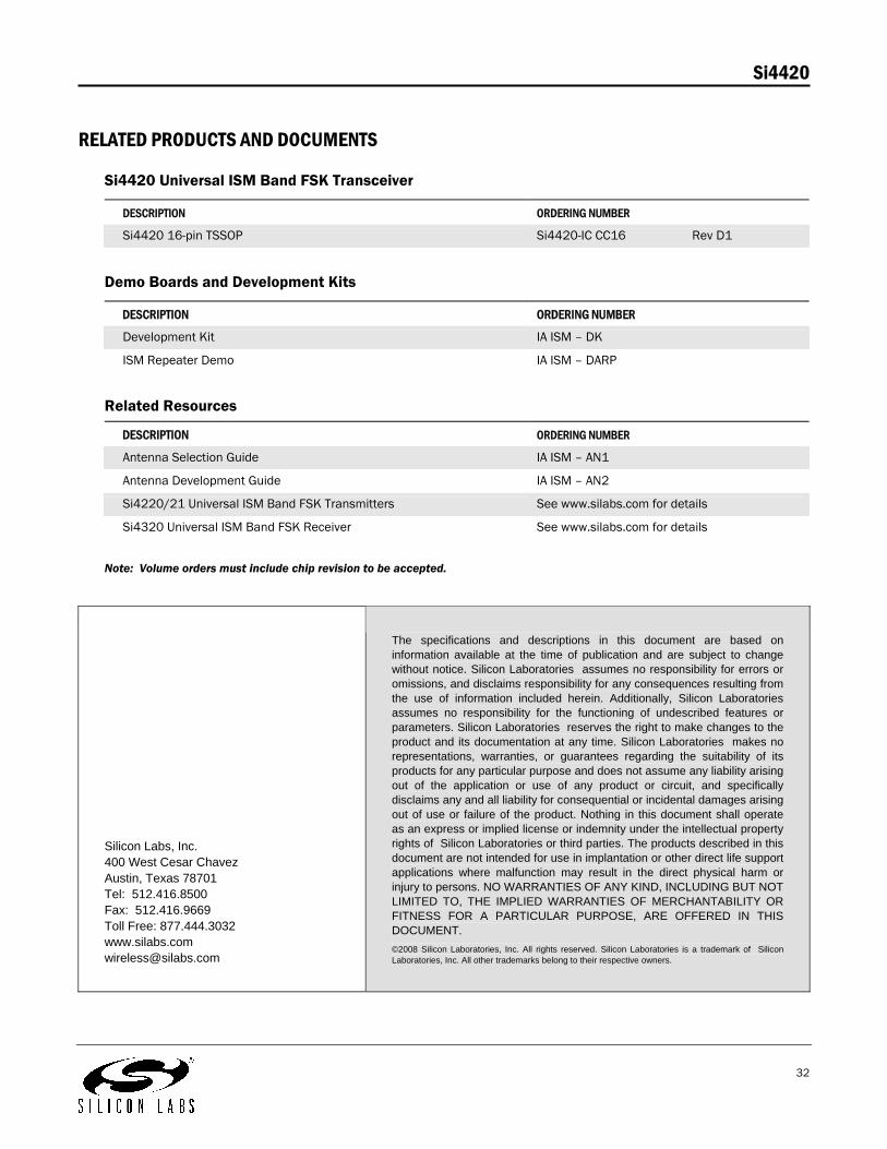
RELATED PRODUCTS AND DOCUMENTS
Si4420 Universal ISM Band FSK Transceiver
DESCRIPTION ORDERING NUMBER
Si4420 16-pin TSSOP Si4420-IC CC16 Rev D1
Demo Boards and Development Kits
DESCRIPTION ORDERING NUMBER Development Kit IA ISM – DK ISM Repeater Demo IA ISM – DARP
Related Resources
DESCRIPTION ORDERING NUMBER
Antenna Selection Guide IA ISM – AN1 Antenna Development Guide IA ISM – AN2 Si4220/21 Universal ISM Band FSK Transmitters See www.silabs.com for details Si4320 Universal ISM Band FSK Receiver See www.silabs.com for details
Note: Volume orders must include chip revision to be accepted.
Silicon Labs, Inc. 400 West Cesar Chavez Austin, Texas 78701 Tel: 512.416.8500 Fax: 512.416.9669 Toll Free: 877.444.3032 www.silabs.com [email protected]
The specifications and descriptions in this document are based on information available at the time of publication and are subject to change without notice. Silicon Laboratories assumes no responsibility for errors or omissions, and disclaims responsibility for any consequences resulting from the use of information included herein. Additionally, Silicon Laboratories assumes no responsibility for the functioning of undescribed features or parameters. Silicon Laboratories reserves the right to make changes to the product and its documentation at any time. Silicon Laboratories makes no representations, warranties, or guarantees regarding the suitability of its products for any particular purpose and does not assume any liability arising out of the application or use of any product or circuit, and specifically disclaims any and all liability for consequential or incidental damages arising out of use or failure of the product. Nothing in this document shall operate as an express or implied license or indemnity under the intellectual property rights of Silicon Laboratories or third parties. The products described in this document are not intended for use in implantation or other direct life support applications where malfunction may result in the direct physical harm or injury to persons. NO WARRANTIES OF ANY KIND, INCLUDING BUT NOT LIMITED TO, THE IMPLIED WARRANTIES OF MERCHANTABILITY OR FITNESS FOR A PARTICULAR PURPOSE, ARE OFFERED IN THIS DOCUMENT.
©2008 Silicon Laboratories, Inc. All rights reserved. Silicon Laboratories is a trademark of Silicon Laboratories, Inc. All other trademarks belong to their respective owners.