Si3406x Family Data Sheet - Mouser Electronics · Si3406x Family Data Sheet Fully-Integrated...
19
Si3406x Family Data Sheet Fully-Integrated 802.3-Compliant POE+ PD Interface and High- Efficiency Switching Regulators with Transistor Bypass, Sleep, Wake, and LED Drive The Si3406x family integrates all power management and control functions required in a Power-over-Ethernet Plus (PoE+) powered device (PD) application. These devices convert the high voltage supplied over the 10/100/1000BASE-T Ethernet connection to a regulated, low-voltage output supply. The optimized architecture of this device family minimizes the solution footprint and external BOM cost and enables the use of low-cost external components while maintaining high performance. The Si3406x family integra- tes the required diode bridges and transient surge suppressor, thus enabling direct connection of the IC to the Ethernet RJ-45 connector. The switching power FET and all associated functions are also integrated. The integrated, current mode controlled switching regulator supports isolated or non-isolated flyback and buck converter topolo- gies. The switching frequency for the regulator is tunable with a simple external resistor value to help avoid unwanted harmonics and includes clock spreading support for emissions reduction. A synchronous driver is provided to optionally drive a secondary side FET to improve efficiency of power conversion. Connection to the PSE switch is maintained during sleep by an optional automated maintain-power-signature (MPS) sig- nal. These devices fully support the IEEE 802.3at specification for the cases of single or two event classification. Standard external resistors provide the proper 802.3 signa- tures for the detection function and programming of the classification mode, and inter- nal startup circuits ensure well-controlled soft-start initial operation of both the hotswap switch and the voltage regulator. The Si34061 and Si34062 add auxiliary main transformer winding support for ultra- high-efficiency operation. The Si34061 includes support for external augmentation or full bypass of the internal hotswap and/or switching FET for best power handling and thermal management at the high end of Class 4, plus offers a further boost in power conversion efficiency when needed. The Si34062 includes support for sleep modes with wake function, as well as LED drive capability. These features can be utilized to minimize standby current, control sleep and wake states, and provide application status information using a solid or blinking LED. The Si3406 is available in a low-profile, 20-pin, 5 x 5 mm QFN package, and the Si34061 and Si34062 are available in low-profile, 24-pin, 5 x 5 mm QFN packages. KEY FEATURES • Type 1 (PoE) or Type 2 (PoE+) power • Full IEEE 802.3at compliance • Synchronous secondary FET driver • Current mode dc-dc converter • Tunable switching frequency with clock spreading • Auxiliary transformer winding support • Auxiliary adapter support • Internal hotswap and switching FET bypass support • Automated maintain-power-signature (MPS) support • Sleep mode augmented with wake pin, mode control, and LED driver • 120 V Absolute Max voltage performance • Industrial –40 to +85 °C temperature • Compact ROHS-compliant 5 mm x 5 mm QFN Package APPLICATIONS • Voice over IP telephones • Wireless access points • Security and surveillance IP cameras • Lighting luminaires • Point-of-sale terminals • Internet appliances • Network devices silabs.com | Smart. Connected. Energy-friendly. Preliminary Rev. 0.1 This information applies to a product under development. Its characteristics and specifications are subject to change without notice.
Transcript of Si3406x Family Data Sheet - Mouser Electronics · Si3406x Family Data Sheet Fully-Integrated...

Si3406x Family Data Sheet
Fully-Integrated 802.3-Compliant POE+ PD Interface and High-Efficiency Switching Regulators with Transistor Bypass, Sleep,Wake, and LED DriveThe Si3406x family integrates all power management and control functions required ina Power-over-Ethernet Plus (PoE+) powered device (PD) application. These devicesconvert the high voltage supplied over the 10/100/1000BASE-T Ethernet connection toa regulated, low-voltage output supply. The optimized architecture of this device familyminimizes the solution footprint and external BOM cost and enables the use of low-costexternal components while maintaining high performance. The Si3406x family integra-tes the required diode bridges and transient surge suppressor, thus enabling directconnection of the IC to the Ethernet RJ-45 connector. The switching power FET and allassociated functions are also integrated. The integrated, current mode controlledswitching regulator supports isolated or non-isolated flyback and buck converter topolo-gies. The switching frequency for the regulator is tunable with a simple external resistorvalue to help avoid unwanted harmonics and includes clock spreading support foremissions reduction. A synchronous driver is provided to optionally drive a secondaryside FET to improve efficiency of power conversion. Connection to the PSE switch ismaintained during sleep by an optional automated maintain-power-signature (MPS) sig-nal.
These devices fully support the IEEE 802.3at specification for the cases of single ortwo event classification. Standard external resistors provide the proper 802.3 signa-tures for the detection function and programming of the classification mode, and inter-nal startup circuits ensure well-controlled soft-start initial operation of both the hotswapswitch and the voltage regulator.
The Si34061 and Si34062 add auxiliary main transformer winding support for ultra-high-efficiency operation.
The Si34061 includes support for external augmentation or full bypass of the internalhotswap and/or switching FET for best power handling and thermal management at thehigh end of Class 4, plus offers a further boost in power conversion efficiency whenneeded.
The Si34062 includes support for sleep modes with wake function, as well as LED drivecapability. These features can be utilized to minimize standby current, control sleepand wake states, and provide application status information using a solid or blinkingLED.
The Si3406 is available in a low-profile, 20-pin, 5 x 5 mm QFN package, and theSi34061 and Si34062 are available in low-profile, 24-pin, 5 x 5 mm QFN packages.
KEY FEATURES
• Type 1 (PoE) or Type 2 (PoE+) power• Full IEEE 802.3at compliance• Synchronous secondary FET driver• Current mode dc-dc converter• Tunable switching frequency with clock
spreading• Auxiliary transformer winding support• Auxiliary adapter support• Internal hotswap and switching FET bypass
support• Automated maintain-power-signature (MPS)
support• Sleep mode augmented with wake pin,
mode control, and LED driver• 120 V Absolute Max voltage performance• Industrial –40 to +85 °C temperature• Compact ROHS-compliant 5 mm x 5 mm
QFN Package
APPLICATIONS
• Voice over IP telephones• Wireless access points• Security and surveillance IP cameras• Lighting luminaires• Point-of-sale terminals• Internet appliances• Network devices
silabs.com | Smart. Connected. Energy-friendly. Preliminary Rev. 0.1 This information applies to a product under development. Its characteristics and specifications are subject to change without notice.

1. System Overview
1.1 Block Diagrams
Figure 1.1. Si3406 Block Diagram
Figure 1.2. Si34061 Block Diagram
Figure 1.3. Si34062 Block Diagram
Si3406x Family Data SheetSystem Overview
silabs.com | Smart. Connected. Energy-friendly. Preliminary Rev. 0.1 | 1

1.2 Power over Ethernet (PoE) Line-Side Interface
The PoE line interface consists of diode bridges and surge protection. The internal diode bridge maximum current is given by the speci-fication, IRECT. If the application needs to consume more current from the power interface, an external diode bridge has to be used withSchottky diodes. The external bridge should be connected in parallel to the internal bridge and the designer must ensure that the inter-nal bridge will not conduct significant current by using low-voltage-drop external diodes.
The chip features active protection against surge transients and accidentally applied telephony voltages. The protection circuit is activa-ted if the VPOS-VNEG voltage exceeds TPROT and the hot swap switch is off (dcdc is not powered). If the hot swap switch is on, thesurge power is sunk in the dcdc’s capacitance.
The internal surge protection can be overridden with an external TVS if higher than specified surge conditions need be tolerated. Theexternal surge device must be connected in parallel to the internal one; therefore, the designer must ensure that the external surgeprotection will activate prior to the internal surge protection.
1.3 Hot Swap Switch
The internal hot swap switch is turned on (closed) when the PoE interface voltage goes above VUVLO_R. It provides limited inrush cur-rent until the dcdc side capacitor is charged. The hot swap switch turns off (open) if voltage on the switch is greater than VHSSW_OFF.
In overload, the hot swap switch goes into current-limiting mode with a current limit of IOVL. It can turn back on after TWAITHSSW elap-ses, the dcdc capacitor is recharged, and HSO-VSS voltage is less or greater than VHSSW_ON.
The hot swap switch (if it is in the on state and conducting) can detect if the current is lower than IMPSth. In this case, the chip turns onMPS pulse generation, which ensures that the PSE will not disconnect.
With the Si34061, an external hot swap switch can be used to improve efficiency in high current applications. For Class 3 applications,using an external hot swap switch is recommended; for Class 4, it is mandatory because the internal hot swap switch otherwise gener-ates significant heat. When an external hot swap switch is used, intelligent switch control ensures that inrush current limiting and auto-matic MPS request of the internal switch are still supported.
1.4 DC to DC Converter
The dc-to-dc converter is current-controlled for easier compensation and more robust protection of circuit magnetics. The controller hasthe following features:• High- and low-side feedback (supports buck and flyback topologies).• <1 Ω internal switching FET• Driver for optional synchronous rectification• Overcurrent detection• Low current detection• Cycle skipping at low current and short circuit conditions• Optional external switching FET driver (Si34061)
When the internal switching FET is used with the converter, internal peak current detection is employed. When the EXTGD pin and anexternal FET are used with Si34061, an external current sense resistor is used to measure the peak current. Changing that resistorallows the application to set the converter maximum current to protect the magnetic components like the transformer.
Feedback to the dcdc converter can be provided in three ways:• High side, referenced to VPOS, connected to FBH pin (buck converter)• Low side, referenced to VSS, connected to FBL pin (nonisolated flyback)• Directly to EROUT pin by a voltage to current converter (isolated flyback)
The EROUT pin provides current output (if FBL or FBH is used) and voltage input. Also, the loop compensation impedance is connec-ted to EROUT. The active voltage range is VEROUT, which is proportional to the converter peak current.
The converter startup is not configurable; soft start is accomplished by internal circuitry. Soft start time is TSOFTSTART.
Si3406x Family Data SheetSystem Overview
silabs.com | Smart. Connected. Energy-friendly. Preliminary Rev. 0.1 | 2

1.5 Average Current Sensing, Overcurrent, and Low-Current Detection
The chip current is sensed by an external resistor connected between VSS and ISNS. Overcurrent is detected and triggered when thevoltage on the sense resistor exceeds VISNS_OVC. Sizing the resistor allows the designer to set the overcurrent limit according to appli-cation needs. When overcurrent is triggered, the dcdc controller goes into reset until the overcurrent resolves. When the current goesback to normal, the controller starts up again.
The external resistor is also used to detect a low current situation. When the voltage on the sense resistor goes below VISNS_LC, thedcdc controller disables the sync FET and the external hot swap switch, allowing very low current consumption—the hot swap switchthen measures the chip current internally. If the chip current is lower than the PoE maintain power signature (MPS) limit, and if automat-ic sleep mode is enabled, the chip turns on the MPS generation. See the sleep mode section for further detail.
1.6 Sync FET Driver
The synchronous rectifying FET driver is always enabled in si3406 configurations, but, if the synchronous FET is not, the SYNCL pinmust not be connected. The driver is disabled only when the dcdc converter measures low average current (meaning lower thanVISNS_LC on ISNS), which ensures low sleep mode current consumption.
1.7 External Switching FET Driver
The chip automatically detects if the EXTGD pin is connected to VSS or to a FET gate at startup. If the external switching FET driverwill not be used (and instead the internal switching FET will be used), the EXTGD pin must be tied to VSS. If a transistor is detected,the external driver will be enabled and the SWO output disabled. In that case, the SWO pin must be not connected. The FET current issensed on an external resistor and connected between the SWISNS and VSS pins.
1.8 Regulators
The chip provides a 5 V output to power LEDs or optocouplers. This is a closed-loop regulator, which ensures accurate output voltage.The 5 V regulator is supplied by an internal 11 V open loop regulator, which also provides power for the external FET gate drivers. The11 V regulator is supplied by a coarse 15 V regulator, which is also open-loop. With the Si34061 and Si34062, the VT15V pin can beused to supply this regulator from an optional auxiliary transformer winding. The advantage of doing so is additional power saving sincethe external FET drivers’ current is not generated from the PoE 50 V but, rather, from a transformer-provided 12–16 V. The applicationmust be designed to ensure that the absolute maximum rating voltage for the VT15V pin is not exceeded.
1.9 Tunable Oscillator
The dcdc frequency can be fixed to 250 kHz or tunable by an external resistor. When tuning is used, spread spectrum is also employed.The dcdc switching is centered about the tuned frequency, but the actual switching varies several Hertz above and below the center, atechnique which improves the electromagnetic interference performance of the customer application.
The tuning resistor must be connected to the RFREQ pin. If RFREQ is grounded, the fixed frequency oscillator will provide clock,FOSCINT, to the dcdc converter; otherwise, the resistor will determine the frequency as shown in the following table.
Table 1.1. Sample Oscillator Frequencies with Various RFREQ Resistor Values
Symbol Parameter (Condition) Min Typ Max
FOSCEXT
RFREQ = 437 kΩ 43 50 61.2
RFREQ = 213 kΩ 86.3 100 121.7
RFREQ = 119 kΩ 150.9 175 211.2
RFREQ = 67.5 kΩ 258.4 300 359.5
RFREQ = 39 kΩ 430.9 500 598.9
RFREQ < 10 kΩ or RFREQ > 1 MΩ DC-DC Clock is 250 kHz.
Si3406x Family Data SheetSystem Overview
silabs.com | Smart. Connected. Energy-friendly. Preliminary Rev. 0.1 | 3

1.10 Sleep Mode
The Si3406, Si34061, and Si34062 have automatic and non-automatic sleep modes. When SLEEPb is tied to ground, the automaticsleep mode is enabled, meaning that if the current consumption is lower than IMPSth, the chip will automatically generate MPS pulsesto the PSE. If SLEEPb is tied to VDD, then it will not generate MPS pulses, and the PSE will disconnect if total application currentconsumption drops below 5–10 mA.
For non-automatic sleep mode, tie SLEEPb high at initial startup (right after the hot swap switch turns on). The chip turns OFF automat-ic mode, but pulling SLEEPb low will force MPS generation as long as the pin is held low.
Si3406x Family Data SheetSystem Overview
silabs.com | Smart. Connected. Energy-friendly. Preliminary Rev. 0.1 | 4

1.11 Extended Sleep Mode
In the Si34062, an extended sleep mode is available which includes LED, WAKE, and MODE pin support. The LED pin drives a lightemitting diode to, for example, illuminate a button on the application. The WAKE pin triggers wakeup, and the MODE button controls ifMPS generation is enabled in sleep. In the Si34062 case, SLEEPb is used to initiate sleep.
The sleep mode is initiated by a negative transition on SLEEPb. It is latched at that negative transition event together with MODE, sotheir status is kept until wakeup even if the input changes on these pins due to the secondary side losing power. MPS generation isenabled if MODE = 0 at the SLEEPb transition.
The following figure shows the Si34062 sleep mode behavior.
Figure 1.4. Si34062 Extended Sleep Mode Behavior
The following figure shows the connectivity for the Si34062 with the extended sleep mode.
Figure 1.5. Si34062 with Extended Sleep Mode
Si3406x Family Data SheetSystem Overview
silabs.com | Smart. Connected. Energy-friendly. Preliminary Rev. 0.1 | 5

2. Electrical Specifications
Table 2.1. Absolute Maximum Ratings1
Type Description Min Max Units
Voltage
CT1–CT2 or SP1–SP2 –100 100 V
VNEG-VSS, VPOS- VNEG, HSO2, RDET3 –0.7 100 V
SWO-VSS –0.7 120 V
ISNS, SWISNS –1 1 V
Low Voltage pins: FBH3, EROUT, FBL,VDD, NSLEEP, RCL, RFREQ, NT2P, AS-
UP, WAKE, MODE, LED–0.7 6 V
Mid Voltage pins: SYNCL, V11, VT15V,EXTGD, EXTHSSW –0.7 18 V
Peak Current CT1, CT2, SP1, SP2, VPOS –TBD TBD A
DC Current4 CT1, CT2, SP1, SP2 –0.2 0.2 A
TemperatureStorage Temperature –65 150
°CAmbient Operating Temperature –40 85
Note:1. Unless otherwise noted, all voltages referenced to VSS. Permanent device damage may occur if the maximum ratings are excee-
ded. Functional operation should be restricted to those conditions specified in the operational sections of this data sheet. Expo-sure to absolute maximum rating conditions for extended periods may adversely affect device reliability.
2. Voltage referenced to VNEG.3. Voltage referenced to VPOS.4. Higher dc current is possible in the application, but only utilizing external bridge diodes. Refer to reference design documentation
for further detail.
Si3406x Family Data SheetElectrical Specifications
silabs.com | Smart. Connected. Energy-friendly. Preliminary Rev. 0.1 | 6
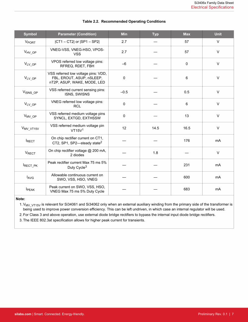
Table 2.2. Recommended Operating Conditions
Symbol Parameter (Condition) Min Typ Max Unit
VPORT |CT1 – CT2| or |SP1 – SP2| 2.7 — 57 V
VHV_OPVNEG-VSS, VNEG-HSO, VPOS-
VSS 2.7 — 57 V
VLV_OPVPOS referred low voltage pins:
RFREQ, RDET, FBH –6 — 0 V
VLV_OP
VSS referred low voltage pins: VDD,FBL, EROUT, ASUP, nSLEEP,
nT2P, ASUP, WAKE, MODE, LED0 — 6 V
VISNS_OPVSS referred current sensing pins:
ISNS, SWISNS –0.5 — 0.5 V
VLV_OPVNEG referred low voltage pins:
RCL 0 — 6 V
VMV_OPVSS referred medium voltage pins
SYNCL, EXTGD, EXTHSSW 0 — 13 V
VMV_VT15VVSS referred medium voltage pin
VT15V1 12 14.5 16.5 V
IRECTOn chip rectifier current on CT1,CT2, SP1, SP2—steady state2 — — 176 mA
VRECTOn chip rectifier voltage @ 200 mA,
2 diodes — 1.8 — V
IRECT_PKPeak rectifier current Max 75 ms 5%
Duty Cycle3 — — 231 mA
IAVGAllowable continuous current on
SWO, VSS, HSO, VNEG — — 600 mA
IPEAKPeak current on SWO, VSS, HSO,VNEG Max 75 ms 5% Duty Cycle — — 683 mA
Note:1. VMV_VT15V is relevant for Si34061 and Si34062 only when an external auxiliary winding from the primary side of the transformer is
being used to improve power conversion efficiency. This can be left undriven, in which case an internal regulator will be used.2. For Class 3 and above operation, use external diode bridge rectifiers to bypass the internal input diode bridge rectifiers.3. The IEEE 802.3at specification allows for higher peak current for transients.
Si3406x Family Data SheetElectrical Specifications
silabs.com | Smart. Connected. Energy-friendly. Preliminary Rev. 0.1 | 7

Table 2.3. Surge Immunity Ratings1, 2, 3
Symbol Description Rating Unit
HBM ESD JEDEC (JESD22-A114E) ±2 kV
CDM ESD JEDEC (JESD22-C101C) ±500 V
Vsurge_cm4 Common Mode (IEC 61000-4-5) ±4 kV
Vsurge_dm4 Differential (IEC 61000-4-5) ±TBD kV
Vtelephony IEEE 802.3at Clause 33.7.5 175 V
Note:1. Permanent device damage may occur if the maximum ratings are exceeded. Functional operation should be restricted to those
conditions specified in the operational sections of this data sheet. Exposure to absolute maximum rating conditions for extendedperiods may adversely affect device reliability.
2. For more information regarding system-level surge tolerance, refer to “ANXXXX: Robust Electrical Surge Immunity for Si3406xPoE PDs through Integrated Protection".
3. Designs must be compliant with the PCB layout and external component recommendations outlined in the Si3406 EVB User'sGuide and the Si3406 Design Guide.
4. For details on surge testing conditions, please refer to ANXXX.
Table 2.4. Electrical Characteristics
Symbol Parameter (Condition) Min Typ Max Unit
PoE PROTOCOL
Detection
VDET Detection Voltage (at VPORT) 2.7 — 10.1 V
RDET Detect resistor (on RDET pin) –1% 24.3 +1% kΩ
Classification
VRESET Classification Reset (at VPORT) 0 — 2.81 V
VCLASS Classification Voltage (at VPORT) 14.5 — 20.5 V
IPortCLASS
Class 0 (RCLASS = 0 to 681 Ω) 0 — 4 mA
Class 1 (RCLASS = 133 Ω) 9 — 12 mA
Class 2 (RCLASS = 73.2 Ω) 17 — 20 mA
Class 3 (RCLASS = 46.4 Ω) 26 — 30 mA
Class 4 (RCLASS = 33.2 Ω) 36 — 44 mA
Type 2 Classification
VMARK Mark event voltage (at VPORT) 6.9 — 10.1 V
IMARK Mark event current 0.25 TBD 4 mA
Power On and UVLO
VUVLO_R Hotswap closed and converter on — 37 — V
VUVLO_F Hotswap open and converter off — 32 — V
Si3406x Family Data SheetElectrical Specifications
silabs.com | Smart. Connected. Energy-friendly. Preliminary Rev. 0.1 | 8
Symbol Parameter (Condition) Min Typ Max Unit
Thermal Characteristics
Tshd Thermal shutdown — 160 — °C
THYST Thermal shutdown hysteresis — 20 — °C
On-Chip Transient Voltage Suppression/Protection
TPROTTVS protection activation voltage
(VPOS-VNEG) 100 — — V
HOT SWAP SWITCH
Iinrush Inrush current 100 170 200 mA
IMAXHSSWMaximum continuous operating cur-
rent — — 600 mA
VHSSW_ON Switch ON voltage — 380 — mV
VHSSW_OFFSwitch OFF voltage, HSSW goes to
overload cycle — 3.5 — V
IOVLSwitch current limit in OVERLOAD
State 8.7 10.5 12.4 mA
IMPSthMPS signal request current level
threshold 14 20 26 mA
IEXT_DRVExternal hot swap driver peak cur-
rent on EXTHSW pin — — 10 mA
VEXT_DRVExternal hot swap driver voltage on
EXTHSW pin TBD 11 — V
TWAITHSSWWait time in OVERLOAD and type 2
inrush 80 96 116 ms
DC-DC
ISWOPEAKPeak current limit of internal FET
(SWO pin) 2.5 — 3 A
VEXTGDExternal FET drive voltage (EXTGD
pin) 9 11 13 V
IEXTGDExternal FET drive current (EXTGD
pin) — — 500 mA
FOSCINT Using internal Oscillator — 350 — kHz
FOSCEXTUsing external Oscillator, tunable on
pin RFREQ 50 — 500 kHz
DUC Output duty cycle of PWM — TBD 75 %
VDCDCUVLODCDC UVLO level (Minimum adapt-
er voltage) 10.2 10.7 11.3 V
VFBREF FBH and FBL reference voltage — 1.36 — V
VEROUTOperating voltage range of error in-
put 1 — 4 V
VISNS_OVCOvercurrent limit voltage on ISNS
(ref. to VSS) — –270 — mV
VISNS_LCLow current limit voltage on ISNS
(ref. to VSS) — –27 — mV
TSOFTSTART Startup time — 4 — ms
Si3406x Family Data SheetElectrical Specifications
silabs.com | Smart. Connected. Energy-friendly. Preliminary Rev. 0.1 | 9
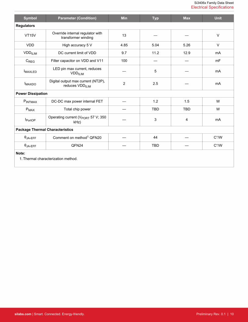
Symbol Parameter (Condition) Min Typ Max Unit
Regulators
VT15V Override internal regulator withtransformer winding 13 — — V
VDD High accuracy 5 V 4.85 5.04 5.26 V
VDDILIM DC current limit of VDD 9.7 11.2 12.9 mA
CREG Filter capacitor on VDD and V11 100 — — mF
IMAXLEDLED pin max current, reduces
VDDILIM— 5 — mA
IMAXDODigital output max current (NT2P),
reduces VDDILIM2 2.5 — mA
Power Dissipation
PINTMAX DC-DC max power internal FET — 1.2 1.5 W
PMAX Total chip power — TBD TBD W
IPortOPOperating current (VPORT 57 V; 350
kHz)— 3 4 mA
Package Thermal Characteristics
θJA-EFF Comment on method1 QFN20 — 44 — C°/W
θJA-EFF QFN24 — TBD — C°/W
Note:1. Thermal characterization method.
Si3406x Family Data SheetElectrical Specifications
silabs.com | Smart. Connected. Energy-friendly. Preliminary Rev. 0.1 | 10

3. Pin Descriptions
Si3406 Pinout (Top View) Si34061 Pinout (Top View) Si34062 Pinout (Top View)
FBH
EROUT
FBL
VDD
SLE
EP
b
RD
ET
SP
2
RC
L
RFR
EQ
SP1
HS
O
VPOS
CT2
CT1
VNEG(Pad)
ISN
S
VS
S
SY
NC
L
T2P
b
V11
SW
O
5 6 7 8 9 10
16 1517181920
1
2
3
4 11
12
13
14
ISNS
EROUT
FBL
VDD
SLE
EP
b
RD
ET
SP
2
RC
L
RFR
EQ
SP1
HS
O
VPOS
CT2
CT1VNEG(Pad)
SW
ISN
S
VS
S
SY
NC
L
V11
SW
O
7 8 9 10
20 1921222324
2
3
4
5
13
14
15
16
11 12
1
6
EXTHSW
ASUP
17
18
T2Pb
VT15
EX
TGD
FBH
EROUT
FBL
VDD
SLE
EP
b
RD
ET
SP
2
RC
L
RFR
EQ
SP1
HS
O
VPOS
CT2
CT1VNEG(Pad)
ISN
S
VS
S
SY
NC
L
V11
SW
O
7 8 9 10
20 1921222324
2
3
4
5
13
14
15
16
11 12
1
6
LED
WAKE
17
18
T2Pb
VT15
MO
DE
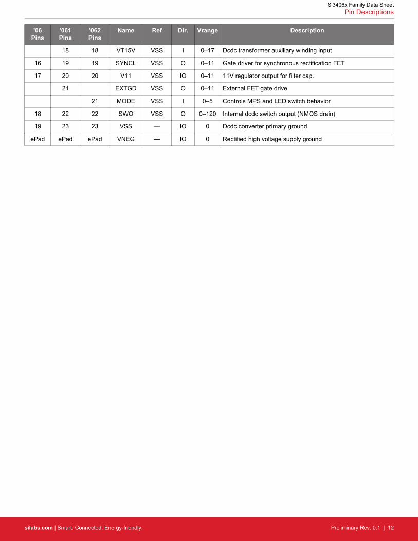
Table 3.1. Pin Descriptions
'06Pins
'061Pins
'062Pins
Name Ref Dir. Vrange Description
24 24 SWISNS VSS I 0–0.5 External FET current sense resistor voltage input
20 1 ISNS VSS I -0.5–0 Chip current sense resistor input
1 1 FBH VPOS I 0–5 High side (VPOS referred) dcdc feedback (buck converter)
2 2 2 EROUT VSS IO 0–5 Error amplifier current output, compensation impedance input
3 3 3 FBL VSS I 0–5 Low side (ground referenced) dcdc feedback (flyback convert-er)
4 4 4 VDD VSS O 0–5 5V regulator output
5 LED VSS O 0–5 Output to drive sleep LED
5 EXTHSW VNEG O 0–11 External hot swap switch drive
6 WAKE VSS I 0–5 Wakeup from sleep mode
6 ASUP VSS I 0–5 AUX auxiliary adapter present
5 7 7 SLEEPb VSS I 0–5 Sleep, with pull-up, driven by open drain
6 8 8 RDET VPOS IO 0–100 Detection resistor
7 9 9 HSO VNEG IO 0–100 Hot swap switch output
8 10 10 RCL VNEG IO 0–5 Classification resistor
9 11 11 RFREQ VPOS IO 0–5 Oscillator frequency tuning resistor, tie to VPOS to select de-fault freq
10 12 12 SP2 SP1 I 0 - 100 High-voltage supply input from spare pair; polarity-insensitive
11 13 13 SP1 SP2 I 0–100 High-voltage supply input from spare pair; polarity-insensitive
12 14 14 VPOS — IO 0–100 Rectified high-voltage supply positive rail
13 15 15 CT2 CT1 I 0–100 High-voltage supply input from main pair; polarity-insensitive
14 16 16 CT1 CT2 I 0 - 100 High-voltage supply input from main pair; polarity-insensitive
15 17 17 T2Pb VSS O 0–5 Type II classification was successful
Si3406x Family Data SheetPin Descriptions
silabs.com | Smart. Connected. Energy-friendly. Preliminary Rev. 0.1 | 11
'06Pins
'061Pins
'062Pins
Name Ref Dir. Vrange Description
18 18 VT15V VSS I 0–17 Dcdc transformer auxiliary winding input
16 19 19 SYNCL VSS O 0–11 Gate driver for synchronous rectification FET
17 20 20 V11 VSS IO 0–11 11V regulator output for filter cap.
21 EXTGD VSS O 0–11 External FET gate drive
21 MODE VSS I 0–5 Controls MPS and LED switch behavior
18 22 22 SWO VSS O 0–120 Internal dcdc switch output (NMOS drain)
19 23 23 VSS — IO 0 Dcdc converter primary ground
ePad ePad ePad VNEG — IO 0 Rectified high voltage supply ground
Si3406x Family Data SheetPin Descriptions
silabs.com | Smart. Connected. Energy-friendly. Preliminary Rev. 0.1 | 12

4. Ordering Guide
Table 4.1. Si3406x Ordering Guide
Ordering Part Number Package Temperature Range (Ambient) Applications
Si3406-A-GM5 x 5 mm 20-QFN
Pb-free, RoHS-compliant–40 to 85 °C Industrial All Purposes
Si34061-A-GM5 x 5 mm 24-QFN
Pb-free, RoHS-compliant–40 to 85 °C Industrial
Any high-power, high-efficiencyuses, such as Wireless Access
Points and IP Cameras
Si34062-A-GM5 x 5 mm 24-QFN
Pb-free, RoHS-compliant–40 to 85 °C Industrial IP Phones or other uses with
Sleep/Green mode
Si3406x Family Data SheetOrdering Guide
silabs.com | Smart. Connected. Energy-friendly. Preliminary Rev. 0.1 | 13

5. Top Markings
5.1 Si3406 Top Marking
Figure 5.1. Si3406 Top Marking
Table 5.1. Si3406 Top Marking Explanation
Mark Method: Laser
Pin 1 Mark: Circle = 0.50 mm Diameter (Lower-Left Corner)
Font Size: 2.0 Point (28 mils)
Line 1 Mark Format: Device Part Number Si3406
Line 2 Mark Format: Device Type A = Device Revision A
G = Extended temperature range
M = QFN package
Line 3 Mark Format: TTTTTT Trace code (assigned by the assembly subcontrac-tor)
Line 4 Mark Format: YY = Year
WW = Work Week
Assembly Year
Assembly Week
Si3406x Family Data SheetTop Markings
silabs.com | Smart. Connected. Energy-friendly. Preliminary Rev. 0.1 | 14

5.2 Si34061 Top Marking
Figure 5.2. Si34061 Top Marking
Table 5.2. Si34061 Top Marking Explanation
Mark Method: Laser
Pin 1 Mark: Circle = 0.50 mm Diameter (Lower-Left Corner)
Font Size: 2.0 Point (28 mils)
Line 1 Mark Format: Device Part Number Si34061
Line 2 Mark Format: Device Type A = Device Revision A
G = Extended temperature range
M = QFN package
Line 3 Mark Format: TTTTTT Trace code (assigned by the assembly subcontrac-tor)
Line 4 Mark Format: YY = Year
WW = Work Week
Assembly Year
Assembly Week
Si3406x Family Data SheetTop Markings
silabs.com | Smart. Connected. Energy-friendly. Preliminary Rev. 0.1 | 15
5.3 Si34062 Top Marking
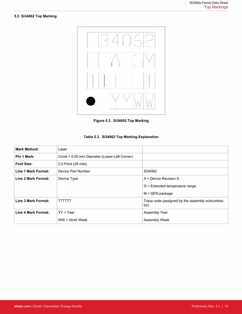
Figure 5.3. Si34062 Top Marking
Table 5.3. Si34062 Top Marking Explanation
Mark Method: Laser
Pin 1 Mark: Circle = 0.50 mm Diameter (Lower-Left Corner)
Font Size: 2.0 Point (28 mils)
Line 1 Mark Format: Device Part Number Si34062
Line 2 Mark Format: Device Type A = Device Revision A
G = Extended temperature range
M = QFN package
Line 3 Mark Format: TTTTTT Trace code (assigned by the assembly subcontrac-tor)
Line 4 Mark Format: YY = Year
WW = Work Week
Assembly Year
Assembly Week
Si3406x Family Data SheetTop Markings
silabs.com | Smart. Connected. Energy-friendly. Preliminary Rev. 0.1 | 16

Table of Contents1. System Overview . . . . . . . . . . . . . . . . . . . . . . . . . . . . . . 1
1.1 Block Diagrams . . . . . . . . . . . . . . . . . . . . . . . . . . . . . 1
1.2 Power over Ethernet (PoE) Line-Side Interface. . . . . . . . . . . . . . . . . . . 2
1.3 Hot Swap Switch . . . . . . . . . . . . . . . . . . . . . . . . . . . . . 2
1.4 DC to DC Converter . . . . . . . . . . . . . . . . . . . . . . . . . . . . 2
1.5 Average Current Sensing, Overcurrent, and Low-Current Detection . . . . . . . . . . . . 3
1.6 Sync FET Driver . . . . . . . . . . . . . . . . . . . . . . . . . . . . . 3
1.7 External Switching FET Driver . . . . . . . . . . . . . . . . . . . . . . . . 3
1.8 Regulators . . . . . . . . . . . . . . . . . . . . . . . . . . . . . . . 3
1.9 Tunable Oscillator . . . . . . . . . . . . . . . . . . . . . . . . . . . . 3
1.10 Sleep Mode . . . . . . . . . . . . . . . . . . . . . . . . . . . . . . 4
1.11 Extended Sleep Mode. . . . . . . . . . . . . . . . . . . . . . . . . . . 5
2. Electrical Specifications . . . . . . . . . . . . . . . . . . . . . . . . . . . 6
3. Pin Descriptions . . . . . . . . . . . . . . . . . . . . . . . . . . . . . 11
4. Ordering Guide . . . . . . . . . . . . . . . . . . . . . . . . . . . . . 13
5. Top Markings . . . . . . . . . . . . . . . . . . . . . . . . . . . . . . 145.1 Si3406 Top Marking . . . . . . . . . . . . . . . . . . . . . . . . . . . .14
5.2 Si34061 Top Marking . . . . . . . . . . . . . . . . . . . . . . . . . . .15
5.3 Si34062 Top Marking . . . . . . . . . . . . . . . . . . . . . . . . . . .16
Table of Contents 17

http://www.silabs.com
Silicon Laboratories Inc.400 West Cesar ChavezAustin, TX 78701USA
Smart.Connected.Energy-Friendly
Productswww.silabs.com/products
Qualitywww.silabs.com/quality
Support and Communitycommunity.silabs.com
DisclaimerSilicon Labs intends to provide customers with the latest, accurate, and in-depth documentation of all peripherals and modules available for system and software implementers using or intending to use the Silicon Labs products. Characterization data, available modules and peripherals, memory sizes and memory addresses refer to each specific device, and "Typical" parameters provided can and do vary in different applications. Application examples described herein are for illustrative purposes only. Silicon Labs reserves the right to make changes without further notice and limitation to product information, specifications, and descriptions herein, and does not give warranties as to the accuracy or completeness of the included information. Silicon Labs shall have no liability for the consequences of use of the information supplied herein. This document does not imply or express copyright licenses granted hereunder to design or fabricate any integrated circuits. The products are not designed or authorized to be used within any Life Support System without the specific written consent of Silicon Labs. A "Life Support System" is any product or system intended to support or sustain life and/or health, which, if it fails, can be reasonably expected to result in significant personal injury or death. Silicon Labs products are not designed or authorized for military applications. Silicon Labs products shall under no circumstances be used in weapons of mass destruction including (but not limited to) nuclear, biological or chemical weapons, or missiles capable of delivering such weapons.
Trademark InformationSilicon Laboratories Inc.® , Silicon Laboratories®, Silicon Labs®, SiLabs® and the Silicon Labs logo®, Bluegiga®, Bluegiga Logo®, Clockbuilder®, CMEMS®, DSPLL®, EFM®, EFM32®, EFR, Ember®, Energy Micro, Energy Micro logo and combinations thereof, "the world’s most energy friendly microcontrollers", Ember®, EZLink®, EZRadio®, EZRadioPRO®, Gecko®, ISOmodem®, Precision32®, ProSLIC®, Simplicity Studio®, SiPHY®, Telegesis, the Telegesis Logo®, USBXpress® and others are trademarks or registered trademarks of Silicon Labs. ARM, CORTEX, Cortex-M3 and THUMB are trademarks or registered trademarks of ARM Holdings. Keil is a registered trademark of ARM Limited. All other products or brand names mentioned herein are trademarks of their respective holders.