SI-8000JD Series - 1.5 A, Buck Converter IC
29
1.5 A, Buck Converter IC SI-8000JD Series Data Sheet SI-8000JD-DSE Rev.2.1 SANKEN ELECTRIC CO., LTD. 1 Sep. 03, 2020 https://www.sanken-ele.co.jp/en © SANKEN ELECTRIC CO., LTD. 2011 Description SI-8000JD series are buck converter ICs whose maximum output current is 1.5 A. These products have various functions including the Output On/Off Function, the Overcurrent Protection and the Thermal Shutdown, and achieve a buck converter circuit with few external components. Features ● High Efficiency 88% (SI-8120JD: VIN = 24 V, IOUT = 0.5 A) ● Few Components ● Downsized Choke Coil (Switching Frequency 125 kHz (typ.)) ● Fixed Output Voltage ● On/Off Function ● Low Supply Current during Output Off ● Protection Functions Overcurrent Protections (OCP): Fold-back Type, Auto-restart Thermal Shutdown (TSD): Auto-restart Typical Application C IN C OUT V IN V OUT 1 2 3 4 5 SI-8000JD VIN SW GND VOS ON/OFF D1 GND GND L1 Package TO263-5L Not to scale Selection Guide Part Number Output Voltage SI-8033JD 3.3 V SI-8050JD 5 V SI-8090JD 9 V SI-8120JD 12 V Applications For the systems requiring power supplies such as: ● Audio Visual Equipment ● Office Automation Equipment (e.g., Printer) ● Onboard power supply
Transcript of SI-8000JD Series - 1.5 A, Buck Converter IC

1.5 A, Buck Converter IC
SI-8000JD Series Data Sheet
SI-8000JD-DSE Rev.2.1 SANKEN ELECTRIC CO., LTD. 1 Sep. 03, 2020 https://www.sanken-ele.co.jp/en © SANKEN ELECTRIC CO., LTD. 2011
Description
SI-8000JD series are buck converter ICs whose
maximum output current is 1.5 A.
These products have various functions including the
Output On/Off Function, the Overcurrent Protection and
the Thermal Shutdown, and achieve a buck converter
circuit with few external components.
Features
● High Efficiency 88%
(SI-8120JD: VIN = 24 V, IOUT = 0.5 A)
● Few Components
● Downsized Choke Coil
(Switching Frequency 125 kHz (typ.))
● Fixed Output Voltage
● On/Off Function
● Low Supply Current during Output Off
● Protection Functions
Overcurrent Protections (OCP): Fold-back Type,
Auto-restart
Thermal Shutdown (TSD): Auto-restart
Typical Application
CIN
COUT
VIN VOUT1 2 3 4 5
SI-8000JD
VIN
SW
GN
D
VO
S
ON
/OF
F
D1
GND GND
L1
Package
TO263-5L
Not to scale
Selection Guide
Part Number Output Voltage
SI-8033JD 3.3 V
SI-8050JD 5 V
SI-8090JD 9 V
SI-8120JD 12 V
Applications
For the systems requiring power supplies such as:
● Audio Visual Equipment
● Office Automation Equipment (e.g., Printer)
● Onboard power supply

SI-8000JD
SI-8000JD-DSE Rev.2.1 SANKEN ELECTRIC CO., LTD. 2 Sep. 03, 2020 https://www.sanken-ele.co.jp/en © SANKEN ELECTRIC CO., LTD. 2011
Contents
Description ------------------------------------------------------------------------------------------------------ 1
Contents --------------------------------------------------------------------------------------------------------- 2
1. Absolute Maximum Ratings ----------------------------------------------------------------------------- 3
2. Thermal Resistance Characteristics ------------------------------------------------------------------- 3
3. Recommended Operating Conditions ----------------------------------------------------------------- 4
4. Electrical Characteristics -------------------------------------------------------------------------------- 5 4.1. SI-8033JD --------------------------------------------------------------------------------------------- 5 4.2. SI-8050JD --------------------------------------------------------------------------------------------- 6 4.3. SI-8090JD --------------------------------------------------------------------------------------------- 7 4.4. SI-8120JD --------------------------------------------------------------------------------------------- 8
5. Block Diagram --------------------------------------------------------------------------------------------- 9
6. Pin Configuration Definitions --------------------------------------------------------------------------- 9
7. Typical Application ------------------------------------------------------------------------------------- 10
8. Physical Dimensions ------------------------------------------------------------------------------------ 11 8.1. Land Pattern Example --------------------------------------------------------------------------- 11
9. Marking Diagram --------------------------------------------------------------------------------------- 12
10. Operational Description ------------------------------------------------------------------------------- 13 10.1. PWM Output Voltage Control------------------------------------------------------------------ 13 10.2. Input/output Current and Inductor Current ------------------------------------------------ 13 10.3. Overcurrent Protection Function (OCP) ----------------------------------------------------- 14 10.4. Thermal Shutdown (TSD) ----------------------------------------------------------------------- 14 10.5. Output On/Off Function ------------------------------------------------------------------------- 14
11. Design Notes ---------------------------------------------------------------------------------------------- 15 11.1. Selecting External Components ---------------------------------------------------------------- 15
11.1.1. Inductor, L1 ---------------------------------------------------------------------------------- 15 11.1.2. Input Capacitor, CIN ------------------------------------------------------------------------ 15 11.1.3. Output Capacitor, COUT -------------------------------------------------------------------- 16 11.1.4. Freewheeling Diode, D1 -------------------------------------------------------------------- 17 11.1.5. Spike Noise Reduction ---------------------------------------------------------------------- 17 11.1.6. Reverse Biasing Protection ---------------------------------------------------------------- 18
11.2. PCB Layout----------------------------------------------------------------------------------------- 18 11.2.1. High Current Line -------------------------------------------------------------------------- 18 11.2.2. Input/ Output Capacitor ------------------------------------------------------------------- 18
11.3. Operational Waveforms Confirmation ------------------------------------------------------- 19 11.4. Thermal Design ------------------------------------------------------------------------------------ 20
12. Pattern Layout Example ------------------------------------------------------------------------------- 21
13. Typical Characteristics --------------------------------------------------------------------------------- 22 13.1. SI-8033JD ------------------------------------------------------------------------------------------- 22 13.2. SI-8050JD ------------------------------------------------------------------------------------------- 23 13.3. SI-8090JD ------------------------------------------------------------------------------------------- 25 13.4. SI-8120JD ------------------------------------------------------------------------------------------- 26 13.6. Thermal Derating Curve ------------------------------------------------------------------------- 28
Important Notes ---------------------------------------------------------------------------------------------- 29

SI-8000JD
SI-8000JD-DSE Rev.2.1 SANKEN ELECTRIC CO., LTD. 3 Sep. 03, 2020 https://www.sanken-ele.co.jp/en © SANKEN ELECTRIC CO., LTD. 2011
1. Absolute Maximum Ratings
Current polarities are defined as follows: current going into the IC (sinking) is positive current (+); current coming
out of the IC (sourcing) is negative current (−). Unless specifically noted, TA = 25 °C.
Parameter Symbol Conditions Rating Unit Remarks
Input Voltage VIN 43 V
Allowable Power Dissipation PD(1) (2) 3 W
Junction Temperature TJ 125 °C
Storage Temperature TSTG −40 to 125 °C
(1) Limited by the thermal shutdown. (2) Glass-epoxy board (40 mm × 40 mm), copper area 100%
2. Thermal Resistance Characteristics
Parameter Symbol Conditions Min. Typ. Max. Unit
Thermal Resistance between Junction
and Ambient θJ-A
Mounted on the board.*
See Figure 2-1.
— — 33.3 °C/W
Thermal Resistance between Junction
and Lead θJ-L — — 3 °C/W
TC
Figure 2-1. Case Temperature Measurement Point
* Glass-epoxy board (40 mm × 40 mm), copper area 100%

SI-8000JD
SI-8000JD-DSE Rev.2.1 SANKEN ELECTRIC CO., LTD. 4 Sep. 03, 2020 https://www.sanken-ele.co.jp/en © SANKEN ELECTRIC CO., LTD. 2011
3. Recommended Operating Conditions
Parameter Symbol Conditions Min. Max. Unit Remarks
Input Voltage VIN
IOUT = 0 A to 1 A 5.3 40 V SI-8033JD
IOUT = 0 A to 1.5 A 6.3 40 V
IOUT = 0 A to 1 A 7 40 V SI-8050JD
IOUT = 0 A to 1.5 A 8 40 V
IOUT = 0 A to 1 A 11 40 V SI-8090JD
IOUT = 0 A to 1.5 A 12 40 V
IOUT = 0 A to 1 A 14 40 V SI-8120JD
IOUT = 0 A to 1.5 A 15 40 V
Output Current * IOUT VIN ≥ VOUT + 3 V 0 1.5 A
Operating Junction Temperature TJOP −30 125 °C
Operating Ambient Temperature* TOP −30 125 °C
* Must be used in the range of thermal derating (see Figure 13-25).

SI-8000JD
SI-8000JD-DSE Rev.2.1 SANKEN ELECTRIC CO., LTD. 5 Sep. 03, 2020 https://www.sanken-ele.co.jp/en © SANKEN ELECTRIC CO., LTD. 2011
4. Electrical Characteristics
4.1. SI-8033JD
Current polarities are defined as follows: a current flow going into the IC (sinking) is positive current (+); and a
current flow coming out of the IC (sourcing) is negative current (−).
Unless otherwise specified, TA = 25 °C.
Parameter Symbol Conditions Min. Typ. Max. Unit
Output Voltage VOUT VIN = 15 V, IOUT = 0.5 A 3.234 3.30 3.366 V
Output Voltage Temperature
Coefficient
ΔVOUT/Δ
T — ±0.5 — mV/°C
Efficiency Η VIN = 15 V, IOUT = 0.5 A — 77 — %
Operating Frequency fO VIN = 15 V, IOUT = 0.5 A — 125 — kHz
Line Regulation VLINE VIN = 8 V to 30 V,
IOUT = 0.5 A — 25 80 mV
Load Regulation VLOAD VIN = 15 V,
IOUT = 0.2 A to 0.8 A — 10 30 mV
Overcurrent Protection Start
Current IS VIN = 15 V 1.6 — — A
ON/OFF Pin Low Level Voltage VONOFF_L — — 0.5 V
ON/OFF Pin Source Current at
Low Level IONOFF_L VONOFF_L = 0 V — — 100 μA
Quiescent Current 1 IQ VIN = 15 V, IOUT = 0 A — 7 — mA
Quiescent Current 2 IQ(OFF) VIN = 15 V,
VONOFF_L = 0.3 A — — 200 μA
Efficiency is calculated by the following equation.
η(%) =VOUT × IOUT
VIN × IIN
× 100

SI-8000JD
SI-8000JD-DSE Rev.2.1 SANKEN ELECTRIC CO., LTD. 6 Sep. 03, 2020 https://www.sanken-ele.co.jp/en © SANKEN ELECTRIC CO., LTD. 2011
4.2. SI-8050JD
Current polarities are defined as follows: a current flow going into the IC (sinking) is positive current (+); and a
current flow coming out of the IC (sourcing) is negative current (−).
Unless otherwise specified, TA = 25 °C.
Parameter Symbol Conditions Min. Typ. Max. Unit
Output Voltage VOUT VIN = 20 V, IOUT = 0.5 A 4.9 5.0 5.1 V
Output Voltage Temperature
Coefficient ΔVOUT/ΔT — ±0.5 — mV/°C
Efficiency η VIN = 20 V, IOUT = 0.5 A — 82 — %
Operating Frequency fO VIN = 20 V, IOUT = 0.5 A — 125 — kHz
Line Regulation VLINE VIN = 10 V to 30 V,
IOUT = 0.5 A — 40 100 mV
Load Regulation VLOAD VIN = 20 V,
IOUT = 0.2 A to 0.8 A — 10 40 mV
Overcurrent Protection Start
Current IS VIN = 20 V 1.6 — — A
ON/OFF Pin Low Level
Voltage VONOFF_L — — 0.5 V
ON/OFF Pin Source Current at
Low Level IONOFF_L VONOFF_L = 0 V — — 100 μA
Quiescent Current 1 IQ VIN = 20 V, IOUT = 0 A — 7 — mA
Quiescent Current 2 IQ(OFF) VIN = 20 V,
VONOFF_L = 0.3 A — 200 μA
Efficiency is calculated by the following equation.
η(%) =VOUT × IOUT
VIN × IIN
× 100
SI-8000JD
SI-8000JD-DSE Rev.2.1 SANKEN ELECTRIC CO., LTD. 7 Sep. 03, 2020 https://www.sanken-ele.co.jp/en © SANKEN ELECTRIC CO., LTD. 2011
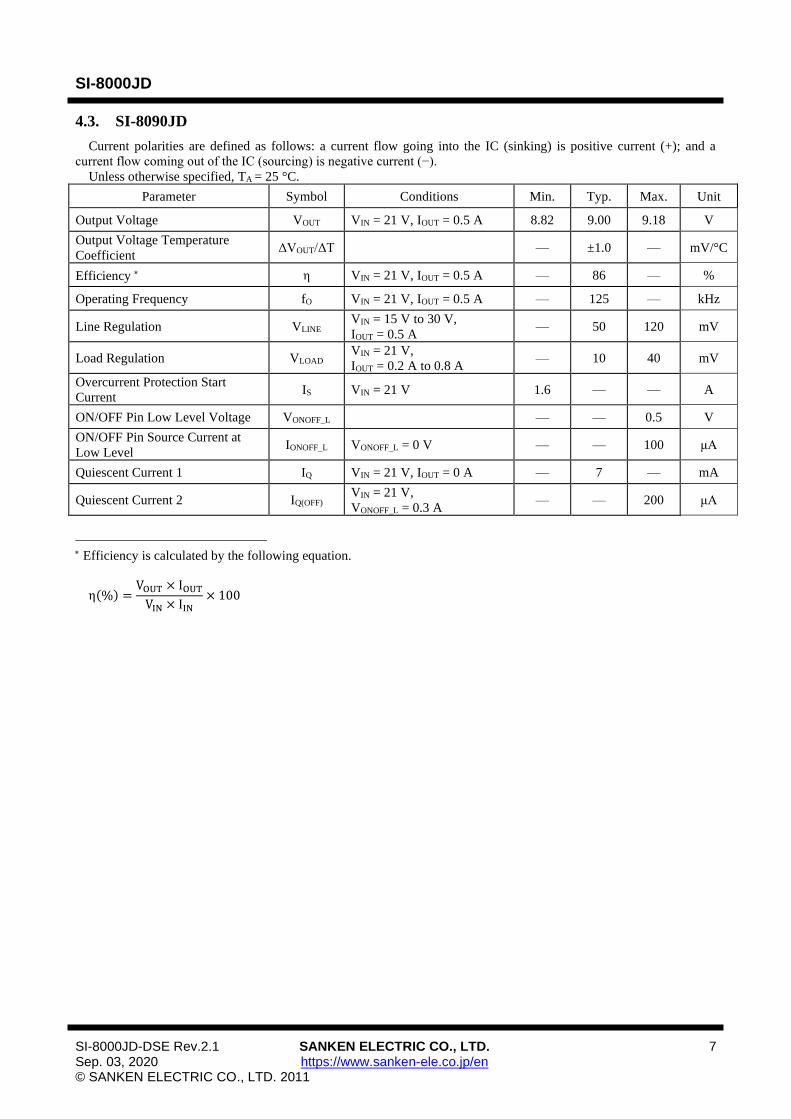
4.3. SI-8090JD
Current polarities are defined as follows: a current flow going into the IC (sinking) is positive current (+); and a
current flow coming out of the IC (sourcing) is negative current (−).
Unless otherwise specified, TA = 25 °C.
Parameter Symbol Conditions Min. Typ. Max. Unit
Output Voltage VOUT VIN = 21 V, IOUT = 0.5 A 8.82 9.00 9.18 V
Output Voltage Temperature
Coefficient ΔVOUT/ΔT — ±1.0 — mV/°C
Efficiency η VIN = 21 V, IOUT = 0.5 A — 86 — %
Operating Frequency fO VIN = 21 V, IOUT = 0.5 A — 125 — kHz
Line Regulation VLINE VIN = 15 V to 30 V,
IOUT = 0.5 A — 50 120 mV
Load Regulation VLOAD VIN = 21 V,
IOUT = 0.2 A to 0.8 A — 10 40 mV
Overcurrent Protection Start
Current IS VIN = 21 V 1.6 — — A
ON/OFF Pin Low Level Voltage VONOFF_L — — 0.5 V
ON/OFF Pin Source Current at
Low Level IONOFF_L VONOFF_L = 0 V — — 100 μA
Quiescent Current 1 IQ VIN = 21 V, IOUT = 0 A — 7 — mA
Quiescent Current 2 IQ(OFF) VIN = 21 V,
VONOFF_L = 0.3 A — — 200 μA
Efficiency is calculated by the following equation.
η(%) =VOUT × IOUT
VIN × IIN
× 100
SI-8000JD
SI-8000JD-DSE Rev.2.1 SANKEN ELECTRIC CO., LTD. 8 Sep. 03, 2020 https://www.sanken-ele.co.jp/en © SANKEN ELECTRIC CO., LTD. 2011
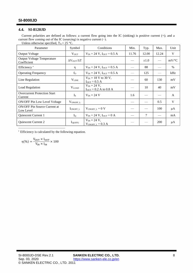
4.4. SI-8120JD
Current polarities are defined as follows: a current flow going into the IC (sinking) is positive current (+); and a
current flow coming out of the IC (sourcing) is negative current (−).
Unless otherwise specified, TA = 25 °C.
Parameter Symbol Conditions Min. Typ. Max. Unit
Output Voltage VOUT VIN = 24 V, IOUT = 0.5 A 11.76 12.00 12.24 V
Output Voltage Temperature
Coefficient ΔVOUT/ΔT — ±1.0 — mV/°C
Efficiency η VIN = 24 V, IOUT = 0.5 A — 88 — %
Operating Frequency fO VIN = 24 V, IOUT = 0.5 A — 125 — kHz
Line Regulation VLINE VIN = 18 V to 30 V,
IOUT = 0.5 A — 60 130 mV
Load Regulation VLOAD VIN = 24 V,
IOUT = 0.2 A to 0.8 A — 10 40 mV
Overcurrent Protection Start
Current IS VIN = 24 V 1.6 — — A
ON/OFF Pin Low Level Voltage VONOFF_L — — 0.5 V
ON/OFF Pin Source Current at
Low Level IONOFF_L VONOFF_L = 0 V — — 100 μA
Quiescent Current 1 IQ VIN = 24 V, IOUT = 0 A — 7 — mA
Quiescent Current 2 IQ(OFF) VIN = 24 V,
VONOFF_L = 0.3 A — — 200 μA
Efficiency is calculated by the following equation.
η(%) =VOUT × IOUT
VIN × IIN
× 100
SI-8000JD
SI-8000JD-DSE Rev.2.1 SANKEN ELECTRIC CO., LTD. 9 Sep. 03, 2020 https://www.sanken-ele.co.jp/en © SANKEN ELECTRIC CO., LTD. 2011
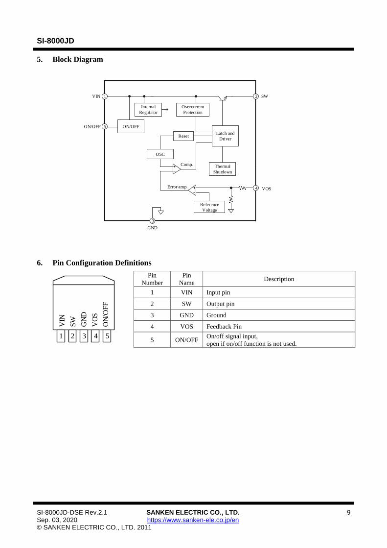
5. Block Diagram
Internal
Regulator
Overcurrent
Protection
Thermal
Shutdown
Reference
Voltage
2
OSC
Reset
Comp.
Error amp.
ON/OFF
GND
VOS
SWVIN
Latch and
Driver
3
4
5
1
ON/OFF
6. Pin Configuration Definitions
1 2 3 4 5
VIN
SW
GN
D
VO
S
ON
/OF
F
Pin
Number
Pin
Name Description
1 VIN Input pin
2 SW Output pin
3 GND Ground
4 VOS Feedback Pin
5 ON/OFF On/off signal input,
open if on/off function is not used.

SI-8000JD
SI-8000JD-DSE Rev.2.1 SANKEN ELECTRIC CO., LTD. 10 Sep. 03, 2020 https://www.sanken-ele.co.jp/en © SANKEN ELECTRIC CO., LTD. 2011
7. Typical Application
CIN COUT
VIN VOUT
1 2 3 4 5
SI-8000JD
VIN
SW
GN
D
VO
S
ON
/OF
F
D1
GND GND
L1
Figure 7-1. Typical Application
Table 7-1. Reference Value of External Components
Symbol Part Type Reference Value Remarks
CIN Electrolytic capacitor 50 V/220 μF See Section 11.1.2.
COUT Electrolytic capacitor 50 V/470 μF See Section 11.1.3.
D1 Schottky diode 60 V, 2 A See Section 11.1.4.
L1 Choke coil 100 μH See Section 11.1.1.

SI-8000JD
SI-8000JD-DSE Rev.2.1 SANKEN ELECTRIC CO., LTD. 11 Sep. 03, 2020 https://www.sanken-ele.co.jp/en © SANKEN ELECTRIC CO., LTD. 2011
8. Physical Dimensions
● TO263-5L
b
b1
c c1
c c
eb
L3
L
A1
A2
H
D
L4
EA
C2L1
(L1)
(E)
E1
D1
PLATING
BASE METAL
SECTION C-C
Symbol Min. Nom. Max.
A 4.40 4.57 4.70
A1 0 0.10 0.25
A2 2.59 2.69 2.79
b 0.77 — 0.90
b1 0.76 0.81 0.86
c 0.34 — 0.47
c1 0.33 0.38 0.43
C2 1.22 — 1.32
D 9.05 9.15 9.25
D1 6.86 — 7.50
E 10.06 10.16 10.26
E1 7.50 — 8.30
e 1.70
BSC
H 14.70 15.10 15.50
L 2.00 2.30 2.60
L1 1.17 1.27 1.40
L3 0.25 BSC
L4 2.00 REF
θ 0° — 8°
θ1 5° 7° 9°
θ2 1° 3° 5°
NOTES:
● Dimensions in millimeters
● Bare lead frame: Pb-free (RoHS compliant)
● Dimensions do not include mold burrs.
8.1. Land Pattern Example
6.8 ±0.1
3.7 ±0.05
4 ±0.1
11 ±0.2
9 ±0.1
1.7 ±0.1 1 ±0.05
9 ±0.2
Dimensions in millimeters

SI-8000JD
SI-8000JD-DSE Rev.2.1 SANKEN ELECTRIC CO., LTD. 12 Sep. 03, 2020 https://www.sanken-ele.co.jp/en © SANKEN ELECTRIC CO., LTD. 2011
9. Marking Diagram
1 5
Specific Device Code
Lot Number
Y is the last digit of the year of manufacture (0 to 9)
M is the month of the year (1 to 9, O, N, or D)
D is the period of days represented by:
1: the first 10 days of the month (1st to 10th)
2: the second 10 days of the month (11th to 20th)
3: the last 1 –11 days of the month (21st to 31st)
XXX is the control number
YMDXXX
Table 9-1. Specific Device Code
Specific Device Code Part Number
8033JD SI-8033JD
8050JD SI-8050JD
8090JD SI-8090JD
8120JD SI-8120JD
(See Table 9-1)

SI-8000JD
SI-8000JD-DSE Rev.2.1 SANKEN ELECTRIC CO., LTD. 13 Sep. 03, 2020 https://www.sanken-ele.co.jp/en © SANKEN ELECTRIC CO., LTD. 2011
10. Operational Description
All the characteristic values given in this section are
typical values, unless they are specified as minimum or
maximum.
10.1. PWM Output Voltage Control
The SI-8000JD series control the output voltage by the
PWM method and have a built-in PWM comparator,
oscillator, error amplifier, reference voltage, output
transistor drive circuit, etc. The PWM comparator
outputs the switching transistor control signal as a square
wave by comparing the triangular wave output (≈125
kHz) from the oscillator with the error amplifier output.
The PWM comparator controls the switching transistor to
turn on during the period when the error amplifier output
exceeds the oscillator output. When the output voltage
rises, the output of the error amplifier decreases because
the error amplifier is an inverting type. When the error
amplifier output decreases, the period below the
oscillator triangle wave level decreases. Thus, the turn-on
period of the switching transistor is shortened. In this
way, the output voltage is regulated by changing the
turn-on time of the switching transistor with the
switching frequency fixed. The higher the VIN, the
shorter the turn-on period of the switching transistor. The
square wave output of the switching transistor is
smoothed by an LC low-pass filter consisting of an
inductor and a capacitor. As a result, a regulated DC
voltage is supplied to the load.
COUT
VOUTSwitching Transistor
D1
L1
Drive
Circuit
PWMComparator
Error Amplifier
ReferenceVoltage
Oscillator
VIN
Figure 10-1. Basic Structure of Switching Regulator
with PWM Control
Oscillator Output
Error Amplifier Output
Switching Transistor OutputON OFF
Figure 10-2. PWM Comparator Operation Diagram
10.2. Input/output Current and Inductor
Current
The square wave output generated by the switching
transistor built in the IC is smoothed by the LC filter
composed of the inductor and the output capacitor, and
converted to the DC output voltage. The operation of the
LC filter significantly affects the stable operation of the
switching regulator. Figure 10-3 shows the schematic
diagram of the current flowing through the circuit, and
Figure 10-4 shows the waveforms of the current flowing
through each element.
COUT
D1
L1
VIN
TR
IDI
ITR IL = ITR + IDI
IOUT
Figure 10-3. Schematic Diagram of Circuit Current
TREmitter Voltage(Switching Output)
IDI
ITR
IL
0IIN
VIN
ΔIL
ILP
ILP
IOUTILP
0
0
TON TOFF
Figure 10-4. Waveforms of Current through Each
Element
As shown in Figure 10-3, the current, IL, flowing
through the inductor has a triangular waveform. This
triangular waveform is composed of two types of current
components, ITR and IDI. The current, ITR, is the current
supplied from the input side through the transistor at
transistor turn-on, and the average value is the input
current, IIN. The current, IDI, is the current that the energy

SI-8000JD
SI-8000JD-DSE Rev.2.1 SANKEN ELECTRIC CO., LTD. 14 Sep. 03, 2020 https://www.sanken-ele.co.jp/en © SANKEN ELECTRIC CO., LTD. 2011
stored in the inductor is commutated through the
freewheeling diode at transistor turn-off.
The inductor current, IL, is the sum of ITR and IDI.
Moreover, the average IL is the DC output current, IOUT,
because the triangular wave component on which IL is
superimposed is smoothed by the capacitor, COUT.
10.3. Overcurrent Protection Function
(OCP)
The IC has the fold-back type overcurrent protection
(OCP) circuit. The overcurrent protection circuit detects
the peak current of the switching transistor. When the
peak current exceeds the set value, the current is limited
by forcibly shortening the on-time of the transistor and
reducing the output voltage. When the output voltage
decreases further to 50% of the rated value, the switching
frequency is decreased to about 40 kHz. As a result, the
current increase at the low output voltage is suppressed.
When the overcurrent state is released, the output voltage
restarts automatically.
Oscillation frequency decreases at this point
Output Voltage
Output Current
Figure 10-5. Overcurrent Protection Characteristics
10.4. Thermal Shutdown (TSD)
The thermal shutdown (TSD) circuit of the IC detects
the junction temperature of the IC. When the junction
temperature exceeds the set value, the TSD turns off the
output by stopping the output transistor. When the
junction temperature drops for about 15 °C from the
thermal shutdown set value, the TSD automatically
restarts the normal operation.
Restart Set Temperature
Output Voltage
Junction Temperature
Protection Set Temperature
Figure 10-6. Thermal Shutdown Characteristics
10.5. Output On/Off Function
Output can be turned on/off using the ON/OFF pin. To
use on/off function, connect a transistor as shown in
Figure 10-7. When the ON/OFF pin voltage decreases to
be VONOFF_L or lower, the output is stopped.
SS
GND
5U1
3
Figure 10-7. On/Off Function
By connecting C3 as shown in Figure 10-8, the rising
delay time is set by using the on/off function. In this case,
the discharge current of C3 flows through the transistor
for on/off function. Therefore, protection such as current
limiting is required when the capacitance of C3 is large.
SS
GND
5U1
3C3
Figure 10-8. Rising Delay Time Setting
The voltage cannot be externally applied because the
ON/OFF pin is pulled up to the internal power supply.
Leave the ON/OFF pin open if the soft start function is
not used.

SI-8000JD
SI-8000JD-DSE Rev.2.1 SANKEN ELECTRIC CO., LTD. 15 Sep. 03, 2020 https://www.sanken-ele.co.jp/en © SANKEN ELECTRIC CO., LTD. 2011
11. Design Notes
11.1. Selecting External Components
11.1.1. Inductor, L1
The inductor, L, supplies the current to the load side at
switching transistor turn-off. For the regulator stable
operation, it is required to avoid saturating the inductor
and excessive self-heating. The following are the key
considerations and the guidelines for selecting an
inductor.
a) An inductor should be for switching regulator
Do not use an inductor for noise filter because it has
a large loss.
b) Rated current
The inductor rated current must be larger than the
maximum load current according to your application.
When the load current exceeds the rated current of
the inductor, the inductance decreases significantly,
resulting in saturation. Note that in this state, the
high frequency impedance decreases and an
excessive current flows.
c) Low noise
In the open magnetic circuit core such as drum type,
the peripheral circuit may be significantly affected
by noise because the magnetic flux passes outside
the coil. It is recommended to use a closed magnetic
circuit core coil such as a toroidal type, EI type, or
EE type.
d) Inductance value should be appropriate
The larger the inductance of the choke coil, the
larger the external size of the coil. On the other hand,
the ripple current flowing through the coil decreases
and the output ripple voltage also decreases (see
Figure 11-1).
The smaller the inductance, the larger the peak
current that flows through the switching transistor or
diode. Thus, the loss increases and the ripple voltage
also increases (see Figure 11-2).
COUT
High Inductance Small Ripple Voltage, Current
Figure 11-1. Ripple Voltage and Current
(High Inductance)
COUT
Low Inductance Large Ripple Voltage, Current
Figure 11-2. Ripple Voltage and Current (Low
Inductance)
Inductance is calculated by the Equation (1).
L =(VIN − VOUT) × VOUT
∆IL × VIN × f (1)
In the Equation, (1), ΔIL shows the ripple current value
of the choke coil, and the reference value is set as
follows:
● When the output current in your application is close to
the maximum rating (1.5 A): 0.2 to 0.3 times the
output current
● When the output current in your application is
approximately 0.5 A or less: 0.5 to 0.6 times the output
current
For example, when VIN = 25 V, VOUT = 5 V,
ΔIL = 0.3 A, and f = 125 kHz, L is calculated as follows:
L =(25 − 5) × 5
0.3 × 25 × 125 × 103≒ 106 μH
Thus, the inductor of about 100 μH should be selected.
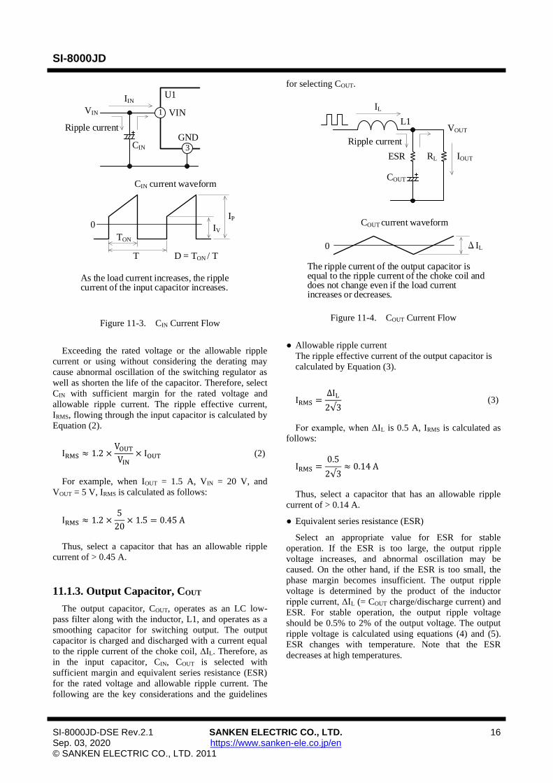
11.1.2. Input Capacitor, CIN
The input capacitor, CIN, operates as a bypass
capacitor for the input circuit. CIN compensates for the
voltage drop in the input side by supplying a steep
current at switching to the regulator. Therefore, CIN
should be placed as close as possible to the IC. When the
smoothing capacitor of AC rectifier circuit is in the input
circuit, the smoothing capacitor can also be used as the
input capacitor.
The following are the key considerations and the
guidelines for selecting CIN.
a) Within the rated voltage
b) Within the allowable ripple current
SI-8000JD
SI-8000JD-DSE Rev.2.1 SANKEN ELECTRIC CO., LTD. 16 Sep. 03, 2020 https://www.sanken-ele.co.jp/en © SANKEN ELECTRIC CO., LTD. 2011
0
IIN
VIN
IV
TON
VIN
GND
1
U1
3CIN
Ripple current
T
IP
CIN current waveform
As the load current increases, the ripple current of the input capacitor increases.
D = TON / T
Figure 11-3. CIN Current Flow
Exceeding the rated voltage or the allowable ripple
current or using without considering the derating may
cause abnormal oscillation of the switching regulator as
well as shorten the life of the capacitor. Therefore, select
CIN with sufficient margin for the rated voltage and
allowable ripple current. The ripple effective current,
IRMS, flowing through the input capacitor is calculated by
Equation (2).
IRMS ≈ 1.2 ×VOUT
VIN
× IOUT (2)
For example, when IOUT = 1.5 A, VIN = 20 V, and
VOUT = 5 V, IRMS is calculated as follows:
IRMS ≈ 1.2 ×5
20× 1.5 = 0.45 A
Thus, select a capacitor that has an allowable ripple
current of > 0.45 A.
11.1.3. Output Capacitor, COUT
The output capacitor, COUT, operates as an LC low-
pass filter along with the inductor, L1, and operates as a
smoothing capacitor for switching output. The output
capacitor is charged and discharged with a current equal
to the ripple current of the choke coil, ΔIL. Therefore, as
in the input capacitor, CIN, COUT is selected with
sufficient margin and equivalent series resistance (ESR)
for the rated voltage and allowable ripple current. The
following are the key considerations and the guidelines
for selecting COUT.
IOUT
VOUT
IL
ESR
Ripple current
0 ΔIL
COUT current waveform
The ripple current of the output capacitor is equal to the ripple current of the choke coil and does not change even if the load current increases or decreases.
COUT
RL
L1
Figure 11-4. COUT Current Flow
● Allowable ripple current
The ripple effective current of the output capacitor is
calculated by Equation (3).
IRMS =∆IL
2√3 (3)
For example, when ΔIL is 0.5 A, IRMS is calculated as
follows:
IRMS =0.5
2√3≈ 0.14 A
Thus, select a capacitor that has an allowable ripple
current of > 0.14 A.
● Equivalent series resistance (ESR)
Select an appropriate value for ESR for stable
operation. If the ESR is too large, the output ripple
voltage increases, and abnormal oscillation may be
caused. On the other hand, if the ESR is too small, the
phase margin becomes insufficient. The output ripple
voltage is determined by the product of the inductor
ripple current, ΔIL (= COUT charge/discharge current) and
ESR. For stable operation, the output ripple voltage
should be 0.5% to 2% of the output voltage. The output
ripple voltage is calculated using equations (4) and (5).
ESR changes with temperature. Note that the ESR
decreases at high temperatures.

SI-8000JD
SI-8000JD-DSE Rev.2.1 SANKEN ELECTRIC CO., LTD. 17 Sep. 03, 2020 https://www.sanken-ele.co.jp/en © SANKEN ELECTRIC CO., LTD. 2011
VRIP ≈(VIN − VOUT) × VOUT
L1 × VIN × f× ESR (4)
VRIP ≈ ∆IL × ESR (5)
If the ESR is too small (about 1 mΩ to 3 mΩ or
less), the phase delay becomes large and abnormal
oscillation may occur. Do not use tantalum capacitors
and monolithic ceramic capacitors alone for COUT as they
have low ESR. When used at low temperature (0 °C or
less), connecting a tantalum capacitor or a laminated
ceramic capacitor in parallel with the electrolytic
capacitor is effective in reducing the output ripple
voltage. In order to further reduce the output ripple
voltage, it is effective to add an LC filter to configure a
pi filter (see Figure 11-5). When an LC filter is added,
connect the point A to the VOS pin so that point A in
Figure 11-5 is the output voltage detection point. If point
A is not set as the output voltage detection point,
abnormal oscillation may occur.
VIN SW
GND
21
U1
3 D1
4VOS
COUT COUT2
L1 L2
A
Figure 11-5. Pi Filter
(L2: 20 μH, COUT2: 200 μF)
The output capacitor should be placed as close as
possible to the IC.
11.1.4. Freewheeling Diode, D1
The freewheel diode is used to release the energy
stored in the inductor at switching off. Be sure to use a
Schottky diode for the freewheeling diode. If a diode
with a long recovery time and a large forward voltage,
such as a general-purpose rectifier diode, is used, a
reverse voltage is applied to the IC, which may damage
the IC.
The voltage output from the SW pin is close to the
input voltage. Therefore, use a freewheeling diode whose
reverse breakdown voltage is higher than the input
voltage. Do not add ferrite beads to the freewheeling
diode.
11.1.5. Spike Noise Reduction
To reduce spike noise, add a noise reduction circuit
between the input and output of the IC and both ends of
the freewheeling diode, D1. Note that the efficiency is
decreased.
When measuring spike noise with an oscilloscope,
connect the probe to the root of the output capacitor with
the shortest probe lead wire. If the probe ground lead
wire is long, the spike noises may be measured
abnormally large because the lead wire acts as an antenna.
VIN SW
GND
0 Ω to 20 Ω
21
U1
3
100 pF to 3000 pF
D1
0 Ω to 20 Ω
100 pF to 4000 pF
Figure 11-6. Spike Noise Reduction
Figure 11-7. Without Noise Reduction Circuit
Figure 11-8. With Noise Reduction Circuit

SI-8000JD
SI-8000JD-DSE Rev.2.1 SANKEN ELECTRIC CO., LTD. 18 Sep. 03, 2020 https://www.sanken-ele.co.jp/en © SANKEN ELECTRIC CO., LTD. 2011
11.1.6. Reverse Biasing Protection
For the applications where the output pin voltage is
higher than the input pin voltage (e.g., battery charger),
add a diode for reverse bias protection between the input
and output.
VIN SW 21
U1
Protection Diode
Figure 11-9. Addition of Reverse Bias Protection
Diode
11.2. PCB Layout
11.2.1. High Current Line
Traces where the switching current flows (bold line in
Figure 11-10) should be as wide and short as possible.
VIN SW
GNDCIN
21U1
3
4VOS
L1
COUT
D1
GND GND
VIN VOUT
Figure 11-10. High Current Line
11.2.2. Input/ Output Capacitor
The input capacitor, CIN, and the output capacitor,
COUT, must be placed as close as possible to the IC.
When CIN and COUT are far from the IC, it may cause
poor regulation or abnormal oscillation due to increased
switching ripple.
When a smoothing capacitor for the AC rectifier
circuit is in the input side, the smoothing capacitor can
also be used as the input capacitor. When the input
smoothing capacitor and the IC are distant, connect an
input capacitor separated from the smoothing capacitor.
Since the large current is charged and discharged to the
input/output capacitor at high speed, the lead wire should
be as short as possible. The pattern of the capacitor
should also be the shortest.
CIN, COUT
Improper Pattern Example Proper Pattern Example
CIN, COUT
Figure 11-11. Pattern Example

SI-8000JD
SI-8000JD-DSE Rev.2.1 SANKEN ELECTRIC CO., LTD. 19 Sep. 03, 2020 https://www.sanken-ele.co.jp/en © SANKEN ELECTRIC CO., LTD. 2011
11.3. Operational Waveforms Confirmation
Whether the switching operation is normal can be
confirmed by the waveform between the SW and GND
pins of the IC. Figure 11-12 shows examples of
waveforms in normal operation and abnormal oscillation.
When the load current is large, the IC operates in
continuous conduction mode. In continuous conduction
mode, the period when the current through inductor
becomes zero does not occur. The switching waveform
has the shape of a normal square wave (waveform 1).
When the load current is small, the IC operates in
discontinuous conduction mode. In discontinuous
conduction mode, the period when the current through
inductor becomes zero occurs. The damped oscillation
occurs in the switching waveform, which is normal
operation (waveform 2).
If the IC and CIN, COUT are distant from each other,
abnormal on/off time of switching is disturbed, and
abnormal oscillation occurs as shown in waveform 3 and
waveform 4.
Figure 11-12. Waveform Examples
異常発振動作(CINが離れている場合) 異常発振動作(COUTが離れている場合)
1. Normal operation (continuous conduction mode) 2. Normal operation (discontinuous conduction mode)
3. Abnormal oscillation (when CIN is distant) 4. Abnormal oscillation (when COUT is distant)

SI-8000JD
SI-8000JD-DSE Rev.2.1 SANKEN ELECTRIC CO., LTD. 20 Sep. 03, 2020 https://www.sanken-ele.co.jp/en © SANKEN ELECTRIC CO., LTD. 2011
11.4. Thermal Design
Generally, the heat dissipation of an IC depends on the
size and material of the board and the copper area. To
improve the thermal performance, the copper area of the
part where the backside of the IC is soldered should be as
large as possible.
Figure 13-25 shows the thermal derating of the IC.
When using the IC, ensure a sufficient margin.
Follow the procedure below to design heat dissipation.
(1) Measure the maximum ambient temperature,
TA(MAX) of the IC.
(2) PD(MAX) is calculated by changing the input/output
conditions and checking the power dissipation, PD.
PD is calculated by Equation (6).
PD = VO × IO (100
η− 1) − VF × IO (1 −
VO
VIN
) (6)
Where:
VOUT is the output voltage
VIN is the input voltage
IOUT is the output current
η is the efficiency (%) (calculated by Figure 13-1 and
Figure 13-7)
VF is D1 forward voltage
(3) Determine the copper area by confirming the
intersection of ambient temperature and power
dissipation by the thermal derating characteristics
shown in Figure 13-25.
For reference, Figure 11-13 shows the relationship
between the copper area and thermal resistance of a
single-sided copper foil board, FR-4.
Copper Area (mm2)
Figure 11-13. Thermal Resistance - Copper Area Reference Characteristics
(Single-sided Copper Foil Board, FR-4)*
* Limited by the condition of the input voltage and output current because the power dissipation of the IC package is
3 W.
Jun
ctio
n-t
o-A
mb
ien
t T
her
mal
Res
ista
nce
, θ
J-A (
°C/W
)
Glass-epoxy Board (40 mm × 40 mm)

SI-8000JD
SI-8000JD-DSE Rev.2.1 SANKEN ELECTRIC CO., LTD. 21 Sep. 03, 2020 https://www.sanken-ele.co.jp/en © SANKEN ELECTRIC CO., LTD. 2011
12. Pattern Layout Example
Connect the ground traces to the GND pin at a single point. Place control components near the IC with a minimal
length of PCB traces.
Figure 12-1. Pattern Layout Example
SI-8000JD
SI-8000JD-DSE Rev.2.1 SANKEN ELECTRIC CO., LTD. 22 Sep. 03, 2020 https://www.sanken-ele.co.jp/en © SANKEN ELECTRIC CO., LTD. 2011
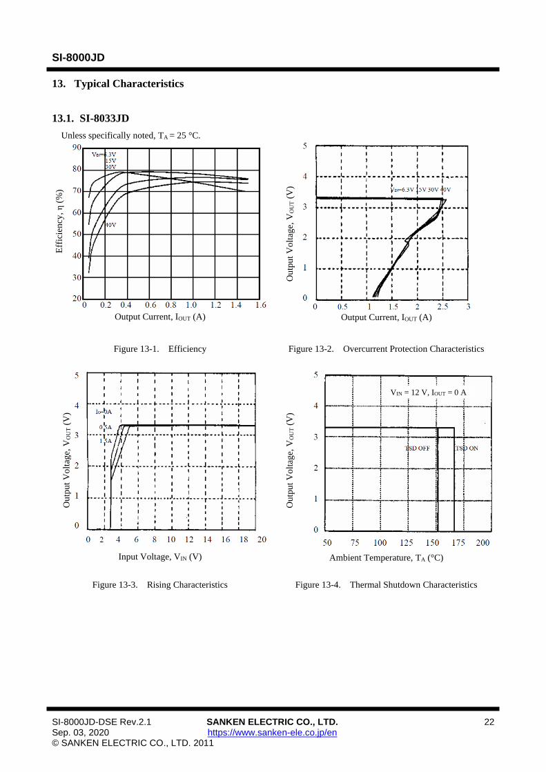
13. Typical Characteristics
13.1. SI-8033JD
Unless specifically noted, TA = 25 °C.
Output Current, IOUT (A)
Output Current, IOUT (A)
Figure 13-1. Efficiency Figure 13-2. Overcurrent Protection Characteristics
Input Voltage, VIN (V)
Ambient Temperature, TA (°C)
Figure 13-3. Rising Characteristics Figure 13-4. Thermal Shutdown Characteristics
Ou
tpu
t V
olt
age,
VO
UT (
V)
Ou
tpu
t V
olt
age,
VO
UT (
V)
Ou
tpu
t V
olt
age,
VO
UT (
V)
Eff
icie
ncy
, η
(%
)
VIN = 12 V, IOUT = 0 A

SI-8000JD
SI-8000JD-DSE Rev.2.1 SANKEN ELECTRIC CO., LTD. 23 Sep. 03, 2020 https://www.sanken-ele.co.jp/en © SANKEN ELECTRIC CO., LTD. 2011
Output Current, IOUT (A)
Ambient Temperature, TA (°C)
Figure 13-5. Load Regulation Figure 13-6. Temperature Characteristic
13.2. SI-8050JD
Unless specifically noted, TA = 25 °C.
Output Current, IOUT (A)
Output Current, IOUT (A)
Figure 13-7. Efficiency Figure 13-8. Overcurrent Protection Characteristics
Ou
tpu
t V
olt
age,
VO
UT (
V)
Ou
tpu
t V
olt
age,
VO
UT (
V)
Fre
qu
ency
(k
Hz)
E
ffic
ien
cy, η
(%
)
VIN = 15 V, IOUT = 0.5 A
Ou
tpu
t V
olt
age,
VO
UT (
V)
Eff
icie
ncy
, η
(%
)

SI-8000JD
SI-8000JD-DSE Rev.2.1 SANKEN ELECTRIC CO., LTD. 24 Sep. 03, 2020 https://www.sanken-ele.co.jp/en © SANKEN ELECTRIC CO., LTD. 2011
Input Voltage, VIN (V)
Ambient Temperature, TA (°C)
Figure 13-9. Rising Characteristics Figure 13-10. Thermal Shutdown Characteristics
Output Current, IOUT (A)
Ambient Temperature, TA (°C)
Figure 13-11. Load Regulation Figure 13-12. Temperature Characteristic
Ou
tpu
t V
olt
age,
VO
UT (
V)
Ou
tpu
t V
olt
age,
VO
UT (
V)
VIN = 20 V, IOUT = 0 A
Ou
tpu
t V
olt
age,
VO
UT (
V)
Ou
tpu
t V
olt
age,
VO
UT (
V)
Fre
qu
ency
(k
Hz)
E
ffic
ien
cy, η
(%
)
VIN = 20 V, IOUT = 1 A
SI-8000JD
SI-8000JD-DSE Rev.2.1 SANKEN ELECTRIC CO., LTD. 25 Sep. 03, 2020 https://www.sanken-ele.co.jp/en © SANKEN ELECTRIC CO., LTD. 2011
13.3. SI-8090JD
Unless specifically noted, TA = 25 °C.
Output Current, IOUT (A)
Output Current, IOUT (A)
Figure 13-13. Efficiency Figure 13-14. Overcurrent Protection Characteristics
Input Voltage, VIN (V)
Ambient Temperature, TA (°C)
Figure 13-15. Rising Characteristics Figure 13-16. Thermal Shutdown Characteristics
Ou
tpu
t V
olt
age,
VO
UT (
V)
Ou
tpu
t V
olt
age,
VO
UT (
V)
Ou
tpu
t V
olt
age,
VO
UT (
V)
Eff
icie
ncy
, η
(%
)
VIN = 21 V, IOUT = 0 A

SI-8000JD
SI-8000JD-DSE Rev.2.1 SANKEN ELECTRIC CO., LTD. 26 Sep. 03, 2020 https://www.sanken-ele.co.jp/en © SANKEN ELECTRIC CO., LTD. 2011
Output Current, IOUT (A)
Ambient Temperature, TA (°C)
Figure 13-17. Load Regulation Figure 13-18. Temperature Characteristic
13.4. SI-8120JD
Unless specifically noted, TA = 25 °C.
Output Current, IOUT (A)
Output Current, IOUT (A)
Figure 13-19. Efficiency Figure 13-20. Overcurrent Protection Characteristics
Ou
tpu
t V
olt
age,
VO
UT (
V)
Ou
tpu
t V
olt
age,
VO
UT (
V)
Fre
qu
ency
(k
Hz)
E
ffic
ien
cy, η
(%
)
VIN = 21 V, IOUT = 0.5 A
Ou
tpu
t V
olt
age,
VO
UT (
V)
Eff
icie
ncy
, η
(%
)

SI-8000JD
SI-8000JD-DSE Rev.2.1 SANKEN ELECTRIC CO., LTD. 27 Sep. 03, 2020 https://www.sanken-ele.co.jp/en © SANKEN ELECTRIC CO., LTD. 2011
Input Voltage, VIN (V)
Ambient Temperature, TA (°C)
Figure 13-21. Rising Characteristics Figure 13-22. Thermal Shutdown Characteristics
Output Current, IOUT (A)
Ambient Temperature, TA (°C)
Figure 13-23. Load Regulation Figure 13-24. Temperature Characteristic
Ou
tpu
t V
olt
age,
VO
UT (
V)
Ou
tpu
t V
olt
age,
VO
UT (
V)
VIN = 24 V, IOUT = 0 A
Ou
tpu
t V
olt
age,
VO
UT (
V)
Ou
tpu
t V
olt
age,
VO
UT (
V)
Fre
qu
ency
(k
Hz)
E
ffic
ien
cy, η
(%
)
VIN = 24 V, IOUT = 1 A

SI-8000JD
SI-8000JD-DSE Rev.2.1 SANKEN ELECTRIC CO., LTD. 28 Sep. 03, 2020 https://www.sanken-ele.co.jp/en © SANKEN ELECTRIC CO., LTD. 2011
13.6. Thermal Derating Curve
Ambient Temperature, TA (°C)
Figure 13-25. Thermal Derating
All
ow
able
Po
wer
Dis
sip
atio
n,
PD (
W)
Copper area 40 mm × 40 mm (θJ-A = 33.3 °C/W)
20 mm × 40 mm (θJ-A = 37 °C/W)
20 mm× 20 mm (θJ-A = 44 °C/W)
10 mm × 10 mm (θJ-A = 53 °C/W)
SI-8000JD
SI-8000JD-DSE Rev.2.1 SANKEN ELECTRIC CO., LTD. 29 Sep. 03, 2020 https://www.sanken-ele.co.jp/en © SANKEN ELECTRIC CO., LTD. 2011
Important Notes
● All data, illustrations, graphs, tables and any other information included in this document (the “Information”) as to Sanken’s
products listed herein (the “Sanken Products”) are current as of the date this document is issued. The Information is subject to any
change without notice due to improvement of the Sanken Products, etc. Please make sure to confirm with a Sanken sales
representative that the contents set forth in this document reflect the latest revisions before use.
● The Sanken Products are intended for use as components of general purpose electronic equipment or apparatus (such as home
appliances, office equipment, telecommunication equipment, measuring equipment, etc.). Prior to use of the Sanken Products,
please put your signature, or affix your name and seal, on the specification documents of the Sanken Products and return them to
Sanken. When considering use of the Sanken Products for any applications that require higher reliability (such as transportation
equipment and its control systems, traffic signal control systems or equipment, disaster/crime alarm systems, various safety
devices, etc.), you must contact a Sanken sales representative to discuss the suitability of such use and put your signature, or affix
your name and seal, on the specification documents of the Sanken Products and return them to Sanken, prior to the use of the
Sanken Products. The Sanken Products are not intended for use in any applications that require extremely high reliability such as:
aerospace equipment; nuclear power control systems; and medical equipment or systems, whose failure or malfunction may result
in death or serious injury to people, i.e., medical devices in Class III or a higher class as defined by relevant laws of Japan
(collectively, the “Specific Applications”). Sanken assumes no liability or responsibility whatsoever for any and all damages and
losses that may be suffered by you, users or any third party, resulting from the use of the Sanken Products in the Specific
Applications or in manner not in compliance with the instructions set forth herein. ● In the event of using the Sanken Products by either (i) combining other products or materials or both therewith or (ii) physically,
chemically or otherwise processing or treating or both the same, you must duly consider all possible risks that may result from all
such uses in advance and proceed therewith at your own responsibility. ● Although Sanken is making efforts to enhance the quality and reliability of its products, it is impossible to completely avoid the
occurrence of any failure or defect or both in semiconductor products at a certain rate. You must take, at your own responsibility,
preventative measures including using a sufficient safety design and confirming safety of any equipment or systems in/for which
the Sanken Products are used, upon due consideration of a failure occurrence rate and derating, etc., in order not to cause any
human injury or death, fire accident or social harm which may result from any failure or malfunction of the Sanken Products.
Please refer to the relevant specification documents and Sanken’s official website in relation to derating. ● No anti-radioactive ray design has been adopted for the Sanken Products. ● The circuit constant, operation examples, circuit examples, pattern layout examples, design examples, recommended examples, all
information and evaluation results based thereon, etc., described in this document are presented for the sole purpose of reference of
use of the Sanken Products. ● Sanken assumes no responsibility whatsoever for any and all damages and losses that may be suffered by you, users or any third
party, or any possible infringement of any and all property rights including intellectual property rights and any other rights of you,
users or any third party, resulting from the Information. ● No information in this document can be transcribed or copied or both without Sanken’s prior written consent.
● Regarding the Information, no license, express, implied or otherwise, is granted hereby under any intellectual property rights and
any other rights of Sanken. ● Unless otherwise agreed in writing between Sanken and you, Sanken makes no warranty of any kind, whether express or implied,
including, without limitation, any warranty (i) as to the quality or performance of the Sanken Products (such as implied warranty
of merchantability, and implied warranty of fitness for a particular purpose or special environment), (ii) that any Sanken Product is
delivered free of claims of third parties by way of infringement or the like, (iii) that may arise from course of performance, course
of dealing or usage of trade, and (iv) as to the Information (including its accuracy, usefulness, and reliability). ● In the event of using the Sanken Products, you must use the same after carefully examining all applicable environmental laws and
regulations that regulate the inclusion or use or both of any particular controlled substances, including, but not limited to, the EU
RoHS Directive, so as to be in strict compliance with such applicable laws and regulations. ● You must not use the Sanken Products or the Information for the purpose of any military applications or use, including but not
limited to the development of weapons of mass destruction. In the event of exporting the Sanken Products or the Information, or
providing them for non-residents, you must comply with all applicable export control laws and regulations in each country
including the U.S. Export Administration Regulations (EAR) and the Foreign Exchange and Foreign Trade Act of Japan, and
follow the procedures required by such applicable laws and regulations. ● Sanken assumes no responsibility for any troubles, which may occur during the transportation of the Sanken Products including
the falling thereof, out of Sanken’s distribution network. ● Although Sanken has prepared this document with its due care to pursue the accuracy thereof, Sanken does not warrant that it is
error free and Sanken assumes no liability whatsoever for any and all damages and losses which may be suffered by you resulting
from any possible errors or omissions in connection with the Information. ● Please refer to our official website in relation to general instructions and directions for using the Sanken Products, and refer to the
relevant specification documents in relation to particular precautions when using the Sanken Products.
● All rights and title in and to any specific trademark or tradename belong to Sanken and such original right holder(s).
DSGN-CEZ-16003