SHARCPAC™ Module Standard Promotes SHARC Multiprocessing
43
SHARCPAC™ Module Standard Promotes SHARC Multiprocessing A four-way collaborative effort culminated in the module interface standard for multiprocessor systems based on Analog Devices ADSP-2106x SHARC digital signal processor. Already adopted by numerous third-party developers, the "SHARCPAC(tm)" standard resulted from contributions made by Ariel Corporation (Highland Park, NJ), Analog Devices (Norwood, MA), BittWare Research Systems (Concord, NH), and Ixthos Incorporated (Leesburg, VA). With 480 MFLOPS delivered in only 13.95 square inches of space, SHARCPAC modules with four SHARCs deliver the industry's highest performance-per-area by a factor of three. Other SHARCPACs provide off-the-shelf processing, memory, and I/O device flexibility for multiprocessor system integrators. "Embedded applications are constantly trying to pack more MFLOPS into less space," said leading DSP observer Will Strauss of Forward Concepts. "The SHARCPAC's improvement on this metric will be heartily welcomed by the industry." The SHARCPAC standard is designed to provide modular, scalable integration for multiprocessor DSP designs. Commercially available SHARCPACs provide a fast way for developers to add DSPs, memory, and I/O to create custom systems using modules that are already established as stable and reliable circuit designs. The royalty-free open standard also allows developers to easily tailor system designs with custom-built SHARCPACs targeted at the functional requirements of particular applications. SHARCPAC building-blocks give developers the easiest way to create custom multiprocessor SHARC systems using off-the-shelf modular components. At more than 34 MFLOPS-per-square-inch, SHARCPACs bring an incredible amount of processing power to the well-proven modular-design approach. SHARCPAC modularity also allows designs to be quickly migrated between various host platforms such as ISA, PCI, and VME. System prototyping and early software development can be accomplished using the SHARCPAC site on the ISA-bus-based EZ-LAB® SHARC Development System from Analog Devices. Ariel Corp. launched the SHARCPAC module initiative with Analog Devices after realizing the dramatic performance-per-area achievable with a SHARC-based module. Ariel define the initial SHARCPAC specification and users' reference guide. Bittware Research Systems and Ixthos participated in finalizing the module specification. BittWare and Alex Computer Systems of Ithaca, New York, were the first companies to market SHARCPAC modules, offering a half-a-dozen variations including single, dual and quad SHARCs, SRAM, and DRAM modules. Now you can access the SHARCPAC specification on the World Wide Web. ### EZ-LAB is a registered trademark and SHARCPAC is a trademark of Analog Devices Corporation
Transcript of SHARCPAC™ Module Standard Promotes SHARC Multiprocessing

SHARCPAC™ Module Standard Promotes SHARC Multiprocessing
A four-way collaborative effort culminated in the module interface standard for multiprocessorsystems based on Analog Devices ADSP-2106x SHARC digital signal processor. Already adopted bynumerous third-party developers, the "SHARCPAC(tm)" standard resulted from contributions made byAriel Corporation (Highland Park, NJ), Analog Devices (Norwood, MA), BittWare Research Systems(Concord, NH), and Ixthos Incorporated (Leesburg, VA).
With 480 MFLOPS delivered in only 13.95 square inches of space, SHARCPAC modules with fourSHARCs deliver the industry's highest performance-per-area by a factor of three. Other SHARCPACsprovide off-the-shelf processing, memory, and I/O device flexibility for multiprocessor systemintegrators.
"Embedded applications are constantly trying to pack more MFLOPS into less space," said leadingDSP observer Will Strauss of Forward Concepts. "The SHARCPAC's improvement on this metric willbe heartily welcomed by the industry."
The SHARCPAC standard is designed to provide modular, scalable integration for multiprocessor DSPdesigns. Commercially available SHARCPACs provide a fast way for developers to add DSPs,memory, and I/O to create custom systems using modules that are already established as stable andreliable circuit designs. The royalty-free open standard also allows developers to easily tailor systemdesigns with custom-built SHARCPACs targeted at the functional requirements of particularapplications.
SHARCPAC building-blocks give developers the easiest way to create custom multiprocessorSHARC systems using off-the-shelf modular components. At more than 34 MFLOPS-per-square-inch,SHARCPACs bring an incredible amount of processing power to the well-proven modular-designapproach.
SHARCPAC modularity also allows designs to be quickly migrated between various host platformssuch as ISA, PCI, and VME. System prototyping and early software development can beaccomplished using the SHARCPAC site on the ISA-bus-based EZ-LAB® SHARC DevelopmentSystem fromAnalog Devices.
Ariel Corp. launched the SHARCPAC module initiative with Analog Devices after realizing thedramatic performance-per-area achievable with a SHARC-based module. Ariel define the initialSHARCPAC specification and users' reference guide. Bittware Research Systems and Ixthosparticipated in finalizing the module specification.
BittWare and Alex Computer Systems of Ithaca, New York, were the first companies to marketSHARCPAC modules, offering a half-a-dozen variations including single, dual and quad SHARCs,SRAM, and DRAM modules.
Now you can access the SHARCPAC specification on the World Wide Web.
###
EZ-LAB is a registered trademark and SHARCPAC is a trademark of AnalogDevices Corporation

Module Specification
Revision 1.2
Revision date:February 22, 1996

SHARCPAC Module Specification Rev. 1.2 – 02/22/96
ii
Published and maintained by:
BittWare Research Systems, Inc.33 N Main St.Concord, NH 03301Phone: (603) 226-0404FAX: (603) 226-6667E-mail: [email protected]
This specification was jointly developed by the following companies:
• Analog Devices, Inc., Norwood, MA
• Ariel Corporation, Highland Park, NJ
• BittWare Research Systems, Inc., Concord, NH
• Ixthos Inc., Leesburg, VA
SHARC and SHARCPAC are trademarks of Analog Devices, Inc.
Rev. 1.2 – 02/22/96 SHARCPAC Module Specification
iii
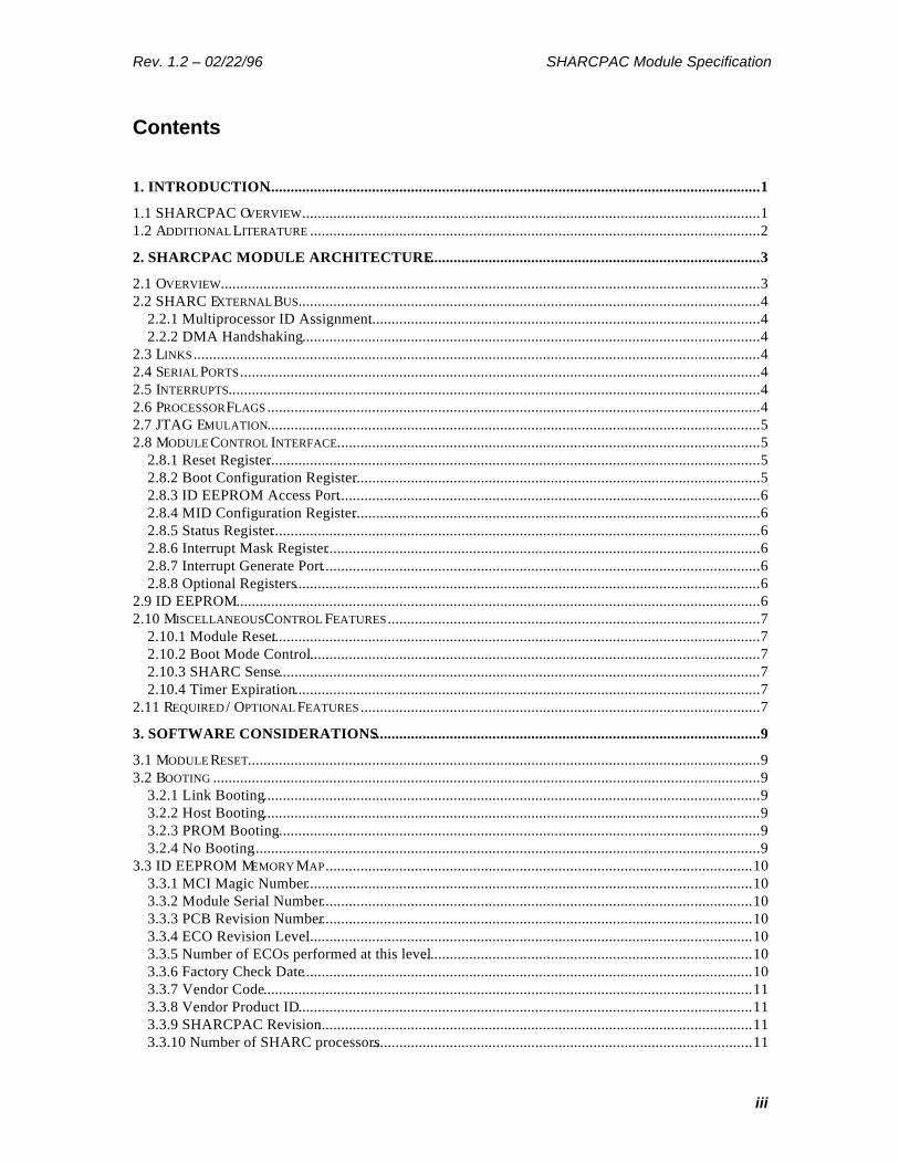
Contents
1. INTRODUCTION...............................................................................................................................1
1.1 SHARCPAC OVERVIEW......................................................................................................................11.2 ADDITIONAL LITERATURE ....................................................................................................................2
2. SHARCPAC MODULE ARCHITECTURE......................................................................................3
2.1 OVERVIEW...........................................................................................................................................32.2 SHARC EXTERNAL BUS.......................................................................................................................4
2.2.1 Multiprocessor ID Assignment.....................................................................................................42.2.2 DMA Handshaking......................................................................................................................4
2.3 LINKS ..................................................................................................................................................42.4 SERIAL PORTS......................................................................................................................................42.5 INTERRUPTS.........................................................................................................................................42.6 PROCESSOR FLAGS ...............................................................................................................................42.7 JTAG EMULATION...............................................................................................................................52.8 MODULE CONTROL INTERFACE.............................................................................................................5
2.8.1 Reset Register...............................................................................................................................52.8.2 Boot Configuration Register.........................................................................................................52.8.3 ID EEPROM Access Port.............................................................................................................62.8.4 MID Configuration Register.........................................................................................................62.8.5 Status Register..............................................................................................................................62.8.6 Interrupt Mask Register................................................................................................................62.8.7 Interrupt Generate Port.................................................................................................................62.8.8 Optional Registers........................................................................................................................6
2.9 ID EEPROM.......................................................................................................................................62.10 MISCELLANEOUS CONTROL FEATURES................................................................................................7
2.10.1 Module Reset..............................................................................................................................72.10.2 Boot Mode Control.....................................................................................................................72.10.3 SHARC Sense............................................................................................................................72.10.4 Timer Expiration........................................................................................................................7
2.11 REQUIRED / OPTIONAL FEATURES .......................................................................................................7
3. SOFTWARE CONSIDERATIONS....................................................................................................9
3.1 MODULE RESET....................................................................................................................................93.2 BOOTING .............................................................................................................................................9
3.2.1 Link Booting................................................................................................................................93.2.2 Host Booting................................................................................................................................93.2.3 PROM Booting.............................................................................................................................93.2.4 No Booting...................................................................................................................................9
3.3 ID EEPROM MEMORY MAP..............................................................................................................103.3.1 MCI Magic Number...................................................................................................................103.3.2 Module Serial Number...............................................................................................................103.3.3 PCB Revision Number................................................................................................................103.3.4 ECO Revision Level...................................................................................................................103.3.5 Number of ECOs performed at this level.....................................................................................103.3.6 Factory Check Date....................................................................................................................103.3.7 Vendor Code..............................................................................................................................113.3.8 Vendor Product ID.....................................................................................................................113.3.9 SHARCPAC Revision................................................................................................................113.3.10 Number of SHARC processors..................................................................................................11

SHARCPAC Module Specification Rev. 1.2 – 02/22/96
iv
3.3.11 Processor Descriptors................................................................................................................113.3.12 Memory Bank Descriptors........................................................................................................113.3.13 Link Descriptors.......................................................................................................................123.3.14 Flag / IRQ Descriptor...............................................................................................................133.3.15 EEPROM Checksum................................................................................................................13
4. ELECTRICAL SPECIFICATIONS.................................................................................................15
4.1 SIGNAL TYPE DEFINITION...................................................................................................................154.2 PIN FUNCTIONAL GROUPS...................................................................................................................16
4.2.1 System Control Signals...............................................................................................................164.2.2 Link Signals...............................................................................................................................174.2.3 Serial Port Signals......................................................................................................................174.2.4 Flag Signals...............................................................................................................................184.2.5 Interrupt Signals.........................................................................................................................184.2.6 JTAG Emulation Signals............................................................................................................184.2.7 External Bus Signals..................................................................................................................194.2.8 Power/Ground Signals................................................................................................................21
4.3 CLOCK DISTRIBUTION AND TERMINATION...........................................................................................214.4 5V VS. 3.3V ......................................................................................................................................214.5 AC TIMING CHARACTERISTICS...........................................................................................................21
4.5.1 Reset Timing..............................................................................................................................214.5.2 MCI Read Timing......................................................................................................................224.5.3 MCI Write Timing.....................................................................................................................22
5. MECHANICAL SPECIFICATIONS...............................................................................................25
5.1 DIMENSIONS......................................................................................................................................255.1.1 Module Dimensions....................................................................................................................255.1.2 Module Site Dimensions.............................................................................................................265.1.3 Module Site Spacing...................................................................................................................265.1.4 Mating Dimensions....................................................................................................................26
5.2 RECOMMENDED CONNECTOR..............................................................................................................275.3 PINOUT..............................................................................................................................................27
5.3.1 Alphabetical List........................................................................................................................285.3.2 Numerical List............................................................................................................................30
6. LIST OF MANUFACTURERS........................................................................................................33
7. SPECIFICATION REVISION HISTORY.......................................................................................35

Rev. 1.2 – 02/22/96 SHARCPAC Module Specification
v
FiguresFigure 2-1 – SHARCPAC Module Architecture........................................................................................3Figure 4-1 – Master Reset (MR) Timing Diagram...................................................................................22Figure 4-2 – MCI Read Timing Diagram................................................................................................22Figure 4-3 – MCI Write Timing Diagram...............................................................................................23Figure 5-1 – SHARCPAC Module Dimensions, Bottom View.................................................................25Figure 5-2 – SHARCPAC Carrier Site Dimensions, Top View................................................................26Figure 5-3 – Mated SHARCPAC Dimensions, Side View........................................................................26
TablesTable 2-1 – MCI Address Map..................................................................................................................5Table 2-2 – Required / Optional SHARCPAC Features.............................................................................7Table 3-1 – Primary SHARC Processor Boot Modes..................................................................................9Table 3-2 – ID EEPROM Data Format....................................................................................................10Table 4-1 – Active State Descriptions for SHARCPAC Signals...............................................................15Table 4-2 – Signal Type Descriptions of the SHARCPAC Module Signals..............................................15Table 4-3 – SHARCPAC Pin Count by Functional Group.......................................................................16Table 4-4 – Master Reset (MR) Timing Parameters.................................................................................21Table 4-5 – MCI Read Timing Parameters..............................................................................................22Table 4-6 – MCI Write Timing Parameters.............................................................................................23Table 5-1 – Mated SHARCPAC Dimensions...........................................................................................27Table 5-2 – Recommended Connectors....................................................................................................27

SHARCPAC Module Specification Rev. 1.2 – 02/22/96
vi

Rev. 1.2 – 02/22/96 SHARCPAC Module Specification
1
1. INTRODUCTIONThis document specifies the mechanical, electrical, and signal requirements for a SHARCPAC™ module.It is intended to provide the system designer all the information necessary to construct a SHARCPACmodule or a SHARCPAC-compatible module site on a host system board. A list of manufacturers thatprovide SHARCPAC-related components and services is presented in section 6.
This section contains a complete overview of the SHARCPAC module, including a discussion of requiredand optional features, and theory of operation. A list of literature relevant to this specification is located atthe end of this section.
1.1 SHARCPAC OVERVIEW
A SHARCPAC Module is a compact, modular solution to satisfy the need within the signal processingcommunity for multiple processors, high speed, and high density of memory and I/O capability. Byoffering a standardized, straightforward, and flexible design, system designers can concentrate onintegration and system-specific issues rather than core DSP/memory design. Modularity also brings theflexibility of upgrading processor types and speeds and memory with little impact on system hardwaredesign.
SHARCPAC Modules were conceived with Analog Devices’ ADSP-2106x Super Harvard ARchitectureComputer (SHARC™) as the processor of choice. The SHARC product family offers a variety of high-performance processors with the following features:
• ADSP-21020 compatible processor core, providing up to 40 MIPS sustained and up to 120MFLOPS peak.
• Up to 4 Megabits of zero wait-state, dual-ported, internal SRAM.
• Three independent internal busses allowing a maximum internal data transfer rate of over 500Mbytes per second.
• Six communications ports providing direct SHARC to SHARC communication capabilities.
• Two synchronous serial ports providing word lengths up to 32 bits, programmable ‘on the fly’ A-law or µ-law companding, and multichannel modes for TDM interfaces.
• 10-channel DMA controller that can be used by link ports, external ports, and the serial ports.
• Intelligent bus interface allowing multiple SHARCs to share the same system bus withoutexternal arbitration or buffer logic.
The SHARCPAC Module is designed to cover a wide range of DSP requirements, without burdening userswith extra unused features or tradeoffs. Modules can have multiple processors, external memory devices,and custom I/O circuitry. Host system boards can be designed with multiple SHARCPAC Module sitesand modules with different capabilities can be installed to create a custom system. The SHARCprocessor’s external system bus is included in the SHARCPAC interface connector to allow directinterprocessor communication and shared memory devices between SHARCPAC resources and systemboard resources.

SHARCPAC Module Specification Rev. 1.2 – 02/22/96
2
1.2 ADDITIONAL LITERATURE
In addition to this specification, the reader is referred to the following publications:
• ADSP-2106x SHARC User’s Manual, available from Analog Devices
• ADSP-21060/62 SHARC Data Sheet, available from Analog Devices
• NM93C46AL 1024-Bit Serial EEPROM Data Sheet, available from National Semiconductor

Rev. 1.2 – 02/22/96 SHARCPAC Module Specification
3
2. SHARCPAC MODULE ARCHITECTUREThe SHARCPAC module can accommodate many different processor and memory device configurations.Its 3.1 × 4.5 inch size allows sufficient space to mount up to four SHARC processors on a single side andsurface mount components can be mounted on both sides of the module (please note the restrictions givenin the section entitled Mechanical Specifications); however, certain characteristics of the moduleconnector interface will influence the architecture of the module.
2.1 OVERVIEW
The primary use for a SHARCPAC module is to provide SHARC processors that can be accessed by thehost system. For this reason, the interface contains all of the external SHARC signals required formultiprocessor connections. SHARC processors on a SHARCPAC module can connect to a cluster ofSHARC processors on the host system or on other SHARCPAC modules (up to 6 processors total percluster) which allows direct memory access through the SHARC external bus (see Figure 2-1). In addition,SHARC link ports, serial ports, flags, and interrupts provide alternate paths for communication andsignaling.
Memory banks can be accessed through the SHARC external bus, making it accessible to all SHARCprocessors in a cluster. The SHARCPAC interface supports up to four memory select signals. Input /output devices may be memory-mapped, connected directly to link ports or serial ports for data exchange.
Modules can be configured and identified through the Module Control Interface. This interface has an 8-bit data interface separate from the SHARC external bus that is accessible to the host system.
The following sections describe each of the SHARCPAC features in more detail.
Figure 2-1 – SHARCPAC Module Architecture

SHARCPAC Module Specification Rev. 1.2 – 02/22/96
4
2.2 SHARC EXTERNAL BUS
The SHARC external bus is the primary method for accessing SHARC processors. It supports the full 32address bits and 48 data bits offered by the SHARC processor. It provides access to other SHARCprocessors connected with the SHARC processor’s built-in bus master arbitration. Host system processorsthat do not have bus-master capability can control the bus with the Host Bus Request (HBR) and Host BusGrant (HBG) signals. Up to six SHARC processors can be selected by these processors using individualchip-select signals. Memory-mapped devices can be selected by the four memory select signals.
2.2.1 Multiprocessor ID AssignmentThe SHARC multiprocessor model defines clusters of up to six processors that share a single external bus.Individual SHARC processors are arbitrated and given access based on their multiprocessor identification(MID) number, which is defined by the ID2-0 pins on the SHARC. Valid MID numbers in a multiprocessorcluster range from 1 to 6. In order to avoid conflicting MID numbers, SHARCPAC modules shouldprovide a method for configuring these numbers for each processor that is connected to the SHARCexternal bus on the SHARCPAC interface. This can be accomplished with jumpers on the module or withregister bits in the Module Control Interface. When default MID numbers are assigned to SHARCPACmodule processors by the designer, the recommended starting number is 6; the recommended startingnumber for SHARC processors on host system boards is 1. The reduces the likelihood of having toreconfigure a SHARCPAC module before a system can be started.
2.2.2 DMA HandshakingA single set of DMA handshaking signals (DMAR / DMAG) is available on the SHARCPAC interface.The signals can be connected directly to the handshaking lines of one of a SHARC processor’s two DMAchannels.
2.3 LINKS
The SHARCPAC interface supports up to 16 off-module links. For purposes of generality they are namedL00 - L15. If less than 16 links go off-module, use of the lower numbered link ports is recommended.Link number zero (L00) must always be connected to the primary SHARC processor’s link port 4 tosupport link booting.
2.4 SERIAL PORTS
The four serial ports available in the SHARCPAC interface are named SP0 - SP3. They allow full-duplexconnections consisting of separate data, frame sync, and clock signals for receive and transmit paths.
2.5 INTERRUPTS
Up to eight interrupt signals from the host system can be connected to SHARC processors on aSHARCPAC module. No special assignments are required, however use of lower-numbered interruptsignals is recommended.
2.6 PROCESSOR FLAGS
Up to eight processor flag signals are available for passing status to and from the host system. Althoughthese signals are bi-directional when connected to the SHARC processor’s flag pins, they may beconnected to devices that are dedicated as inputs or outputs. Input-only devices on SHARCPAC modules(or output-only devices on the host system) should use flag signals 0 - 3. Output-only devices onSHARCPAC modules (or input-only devices on the host system) should use flag signals 4 - 7.

Rev. 1.2 – 02/22/96 SHARCPAC Module Specification
5
2.7 JTAG EMULATION
The SHARCPAC interface supports the standard SHARC in-circuit emulation signals. A JTAG scan paththat originates on the host system board can be routed through devices on the SHARCPAC module andthen routed back to the host board.
2.8 MODULE CONTROL INTERFACE
The Module Control Interface (MCI) provides a method for configuring a module and for providing statusand configuration information to the host system. It is accessed by the host system through a separate 8-bitdata bus. The MCI is optional on SHARCPAC modules; however, it is strongly recommended that amodule implements an MCI. The carrier board is required to support the MCI to ensure compatibility withSHARCPAC modules that need configuration before they can operate.
Four address bits define 16 ports / registers; seven of the ports have reserved functionality as defined bythis specification. The remaining ports can be defined by the module designer. Table 2-1 shows theaddresses of the ports that are defined by this specification.
Table 2-1 – MCI Address Map
AddressAddress Register / PortRegister / Port0x0 Reset Register0x1 Boot Configuration Register0x2 ID EEPROM Access Port0x3 MID Configuration Register0x4 Status Register0x5 Interrupt Mask Register0x6 Interrupt Generate Port
0x7 - 0xF Optional / Module Specific
The individual registers are described in detail below. When a register refers to control or statusinformation for multiple SHARC processors (up to eight), individual SHARC processors are named “A”through “H”. SHARC A should designate the primary SHARC processor on the module.
2.8.1 Reset Register7 6 5 4 3 2 1 0
RSTH RSTG RSTF RSTE RSTD RSTC RSTB RSTA
Each bit in this register is connected to the respective SHARC processor’s reset pin. Writing a zero bringsthe processor into reset, while a one takes it out of reset. The outputs of this register should be logicallycombined with the Master Reset (MR) signal so that when the host system asserts MR, all moduleprocessors are reset.
2.8.2 Boot Configuration Register7 6 5 4 3 2 1 0
BMH BMG BMF BME BMD BMC BMB —
The Boot Configuration register sets the boot mode of the secondary SHARC processors. The boot modeof the primary SHARC processor is programmed with the B0-B1 pins (see 4.2.1, System Control Signals).The following table defines the boot modes for secondary SHARC processors.

SHARCPAC Module Specification Rev. 1.2 – 02/22/96
6
BitBit DSP B-H Boot ModeDSP B-H Boot Mode0 Link booting1 Host booting
2.8.3 ID EEPROM Access Port7 6 5 4 3 2 1 0— — — — EEDO EEDI EESK EECS
EECS (Write-only) Chip SelectEESK (Write-only) Serial Data ClockEEDI (Write-only) Serial Data Input (to EEPROM)EEDO (Read-only) Serial Data Output (from EEPROM)
These register bits are connected directly to the serial EEPROM.
2.8.4 MID Configuration Register7 6 5 4 3 2 1 0— — — — — — — —
These register bits should be used to configure the multiprocessor identification (MID) pins on eachSHARC processor. Specific register bit definitions and MID assignment schemes can be defined by themodule designer.
2.8.5 Status Register7 6 5 4 3 2 1 0— — — — — — — —
These register bits should be used to provide real-time status of the module. Specific register bitdefinitions can be defined by the module designer.
2.8.6 Interrupt Mask Register7 6 5 4 3 2 1 0
IRQH IRQG IRQF IRQE IRQD IRQC IRQB IRQA
These register bits define a mask that controls which processors are interrupted when the host systemaccesses the Interrupt Generate Port. A zero will prevent (mask) the interrupt, while a one will allow theinterrupt to be generated.
2.8.7 Interrupt Generate PortA write to this port causes an interrupt to occur on each of the SHARC processors that are selected in theInterrupt Mask Register. The recommended interrupt pin that should be used on each processor is IRQ0.
2.8.8 Optional RegistersOptional registers are not controlled by this specification. They may be defined by a particular module forany purpose.

Rev. 1.2 – 02/22/96 SHARCPAC Module Specification
7
2.9 ID EEPROMThe ID EEPROM contains module identification and configuration information. The host system canread this information to make a run time determination of the system profile or to perform module-leveltesting. It should be a serial EEPROM, compatible with the National Semiconductor part numberNM93C46AL. It is accessed through the MCI.
2.10 MISCELLANEOUS CONTROL FEATURES
The following sections describe the remaining control features of the SHARCPAC interface.
2.10.1 Module ResetThis signal allows the host system to return the SHARCPAC module to its power-up state.
2.10.2 Boot Mode ControlThe SHARCPAC interface has two pins (B0 - B1) that are programmed by the host system to control thebooting method of the primary SHARC processor (at a minimum). These pins should be programmedprior to releasing the Module Reset signal.
2.10.3 SHARC SenseThis signal provides a method for SHARCPAC modules to indicate to the host system that at least oneSHARC processor is present on the module. The host can detect the state of this signal to changehardware configuration settings. For example, it may redefine MID numbers or reroute the JTAG scanpath.
2.10.4 Timer ExpirationThis signal can be used by the SHARCPAC module to provide a general purpose periodic signal to thehost system. It is usually connected to the TIMEXP output of a SHARC processor on the module.
2.11 REQUIRED / OPTIONAL FEATURES
Table 2-2 lists the major features described in this chapter and whether or not they are required forSHARCPAC module compatibility.

SHARCPAC Module Specification Rev. 1.2 – 02/22/96
8
Table 2-2 – Required / Optional SHARCPAC Features
FeatureFeature ModuleModule Host SiteHost SiteModule Control Interface • Optional • RequiredSHARC external bus • Not required for modules that do not
have memory-mapped devices.• Optional
Link Ports • Primary SHARC must have capability ofbooting from SHARCPAC link 0.
• Primary SHARC must be able to bootremaining SHARC processors.
• Must support booting a SHARCconnected to SHARCPAC link 0.
Serial Ports • Optional • OptionalProcessor Flags • Optional • OptionalInterrupts • Optional • OptionalJTAG signals • At a minimum, must route TDI to TDO if
SENSE is active.• Optional
Boot Mode Signals • Optional • RequiredModule Reset • Required • RequiredSHARC Sense • Optional • OptionalTimer Expiration • Optional • Optional

Rev. 1.2 – 02/22/96 SHARCPAC Module Specification
9
3. SOFTWARE CONSIDERATIONSThis section contains information related to software development for the SHARCPAC module. Issuesthat are discussed cover resetting the module, the different booting modes, accessing the Module ControlInterface, and programming the ID EEPROM.
3.1 MODULE RESET
The SHARCPAC module is placed in reset by asserting the MR (module reset) signal. This immediatelyhalts all SHARC processors and places them in their reset state. The programmer should ensure that theBoot Mode Control signals (B0 - B1) are programmed to the desired values before releasing the MRsignal.
3.2 BOOTING
The Boot Mode Control pins (B0 - B1) set the boot mode for the primary SHARC processor when it comesout of reset. Table 3-1 lists the boot modes defined by the Boot Mode Control pins. Each boot mode isdescribed in the following sections. More detailed information is in the ADSP-2106x SHARC User’sManual.
Table 3-1 – Primary SHARC Processor Boot Modes
B1B1 B0B0 SHARC A Boot ModeSHARC A Boot Mode0 0 Link booting0 1 Host booting1 0 PROM (if available)1 1 No booting (execute from external memory)
3.2.1 Link BootingWhen this mode is selected, the SHARC processor will wait for boot data to arrive at its Link 4. Since theprimary SHARC processor’s Link 4 is always tied to the SHARCPAC interface’s Link 0, the host systemmust provide the bootstrap data via this link port.
3.2.2 Host BootingWhen this mode is selected, the SHARC processor will wait for 16-bit boot data to arrive from externalport buffer zero (EPB0). The host system must provide the boot code through the SHARC processor’sexternal data bus.
3.2.3 PROM BootingWhen this mode is selected, the SHARC processor’s BMS pin becomes an output to be used as a chipselect for an 8-bit EPROM. It will automatically load the bootstrap code from the EPROM.
3.2.4 No BootingWhen this mode is selected, the SHARC processor will start executing instructions from address0x0040 0004 in external memory (bank 0).

SHARCPAC Module Specification Rev. 1.2 – 02/22/96
10
3.3 ID EEPROM MEMORY MAP
The ID EEPROM contains module identification and configuration information. It is a 1024-bit deviceorganized into 64 words that are 16 bits wide. Table 3-2 lists the information that is stored in theEEPROM and the following sections describe the data in detail.
Table 3-2 – ID EEPROM Data Format
LocationLocation DefinitionDefinition0 MCI Magic Number (0xBEEF)
1 - 2 Module Serial Number3 PCB Revision Number4 ECO Revision Level5 Number of ECOs performed at this level
6 - 8 Factory check date9 Vendor Code
10 Vendor Product ID11 SHARCPAC Revision12 Number of SHARC processors on module
13 - 14 Processor Descriptors15 - 18 Memory Bank Descriptors19 - 26 Link Descriptors
27 Flag / IRQ Descriptor28-39 Module Specific
40 EEPROM Checksum41 - 63 User Definable bits
3.3.1 MCI Magic NumberThis location is always programmed to 0xBEEF. Reading 0xBEEF from this location indicates that theEEPROM is programmed and contains valid information.
3.3.2 Module Serial NumberThese two locations contain the 32-bit module serial number. This number is defined by the modulemanufacturer. Location 1 should contain the most significant 16 bits and location 2 should contain theleast significant 16 bits.
3.3.3 PCB Revision NumberThe Printed Circuit Board revision number: 0 = A, 1 = B, 2 = C, etc.
3.3.4 ECO Revision LevelEngineering Change Order revision level. Indicates the level of ECO modifications to the PCB.
3.3.5 Number of ECOs performed at this levelEngineering Change Order minor level. Indicates the number of ECOs performed at the level described inthe ECO Revision Level.
3.3.6 Factory Check DateThese three locations contain the date that the module was tested at the factory. It is assumed that the IDEEPROM will be programmed during factory test. The following table describes the contents of eachlocation.

Rev. 1.2 – 02/22/96 SHARCPAC Module Specification
11
LocationLocation ContentsContents Format / RangeFormat / Range6 Day of month 1 - 317 Month 1 - 128 Year 0 - 9999
3.3.7 Vendor CodeThis 16-bit value identifies the manufacturer of the module. Unique vendor codes are maintained andassigned by Analog Devices (see section 6, List of Manufacturers).
3.3.8 Vendor Product IDThis 16-bit value identifies a particular module within a vendor’s own product line. It may specify amodule family or a specific assembly of a module. These ID numbers are maintained and assigned by themanufacturer of the module.
3.3.9 SHARCPAC RevisionThis specifies the minimum revision level of this SHARCPAC module specification that is required to besupported by the carrier board to operate properly with this module. The most significant 8 bits representsthe major revision number; the least significant 8 bits represents the minor revision number. For example,revision 1.2 would be represented by the value 0x0102.
3.3.10 Number of SHARC processorsThe number of ADSP-2106x SHARC processors installed on the module. This value can range from 0 to8.
3.3.11 Processor DescriptorsThese two locations describe up to eight SHARC processors that are installed on the module. Eachlocation contains four 4-bit codes that identify the processor type and speed of a single processor.
LocationLocation 1515 1414 1313 1212 1111 1010 99 88 77 66 55 44 33 22 11 0013 SHARC D SHARC C SHARC B SHARC A14 SHARC H SHARC G SHARC F SHARC E
CodeCode Processor type and speedProcessor type and speed0000 33 MHz ADSP-210620001 40 MHz ADSP-210620010 33 MHz ADSP-210600011 40 MHz ADSP-21060
All others Reserved for future use.
3.3.12 Memory Bank DescriptorsThese four locations describe up to four memory banks that are installed on the module. The four memorybanks are selected by the MS0-3 signals. Each location contains a 16-bit code that identifies the propertiesof a memory bank. The following table shows the bit fields:
LocationLocation BankBank 1515 1414 1313 1212 1111 1010 99 88 77 66 55 44 33 22 11 0015 0 — R WT_MODE WAIT_STATES DEPTH WIDTH TYPE16 1 — R WT_MODE WAIT_STATES DEPTH WIDTH TYPE17 2 — R WT_MODE WAIT_STATES DEPTH WIDTH TYPE18 3 — R WT_MODE WAIT_STATES DEPTH WIDTH TYPE

SHARCPAC Module Specification Rev. 1.2 – 02/22/96
12
Where the fields are defined as follows:
FieldField DescriptionDescriptionTYPE Memory type: 00 = None, 01 = SRAM, 10 = DRAM, 11 = Other
WIDTH The width of the memory bank in bytes.
DEPTH The depth of the memory is defined the same as the MSIZE field in the SHARC processor’s SYSCONregister, which can be described by:log2(bank size) - 13
WAIT_STATES The number of wait states required for access by the SHARC processor (see table below). This numberis defined the same as the EBxWS field in the SHARC processor’s WAIT register.
WT_MODE The wait state mode required for access by the SHARC processor (see table below). This number isdefined the same as the EMxWM field in the SHARC processor’s WAIT register.
R Indicates whether the memory bank is fixed at the default memory select or if it is relocatable. 0 = Fixed,1 = Relocatable
The WAIT_STATES field has the following definitions:
WAIT_STATEWAIT_STATESS
# of Wait# of WaitStatesStates
Bus IdleBus IdleCycle?Cycle?
Hold TimeHold TimeCycle?Cycle?
000 0 no no001 1 yes no010 2 yes no011 3 yes no100 4 no yes101 5 no yes110 6 no yes111 0 yes no
The WT_MODE field has the following definitions:
WT_MODEWT_MODE Wait State ModeWait State Mode00 External acknowledge only (ACK)01 Internal wait states only10 Both internal and external acknowledge required11 Either internal or external acknowledge sufficient
3.3.13 Link DescriptorsThese eight locations describe up to sixteen links from the SHARCPAC module interface that may beconnected to SHARC processors on the module. Each location describes the destination SHARC processorand link number for two SHARCPAC links.
LocationLocation 1515 1414 1313 1212 1111 1010 99 88 77 66 55 44 33 22 11 0019 Link 1 Proc. # — Link 1 Link # Link 0 Proc. # — Link 0 Link #20 Link 3 Proc. # — Link 3 Link # Link 2 Proc. # — Link 2 Link #21 Link 5 Proc. # — Link 5 Link # Link 4 Proc. # — Link 4 Link #22 Link 7 Proc. # — Link 7 Link # Link 6 Proc. # — Link 6 Link #23 Link 9 Proc. # — Link 9 Link # Link 8 Proc. # — Link 8 Link #24 Link 11 Proc. # — Link 11 Link # Link 10 Proc. # — Link 10 Link #25 Link 13 Proc. # — Link 13 Link # Link 12 Proc. # — Link 12 Link #26 Link 15 Proc. # — Link 15 Link # Link 14 Proc. # — Link 14 Link #

Rev. 1.2 – 02/22/96 SHARCPAC Module Specification
13
Where the fields are defined as follows:
Link x Proc. # This is the processor number to which Link x from the SHARCPAC interface connects.It can range from 0 to 7 (representing SHARC processors “A” to “H”).
Link x Link # This is the link number on the processor specified above to which Link x from theSHARCPAC interface connects. It can range from 0 to 5.
3.3.14 Flag / IRQ DescriptorThis value describes the SHARCPAC module’s use of the interrupt and flag signals. A zero indicates thatthe resource not used; a one indicates that the resource is connected to a device on the module.
1515 1414 1313 1212 1111 1010 99 88 77 66 55 44 33 22 11 00F7 F6 F5 F4 F3 F2 F1 F0 I7 I6 I5 I4 I3 I2 I1 I0
3.3.15 EEPROM ChecksumThis number is used to verify the contents of the ID EEPROM. It is calculated from the sum of all of theprogrammed values in locations 0 to 39, modulo 65536.

SHARCPAC Module Specification Rev. 1.2 – 02/22/96
14

Rev. 1.2 – 02/22/96 SHARCPAC Module Specification
15
4. ELECTRICAL SPECIFICATIONSThis section specifies all of the electrical parameters necessary to properly interface to a SHARCPACmodule. The SHARCPAC interface requires 360 signals for proper implementation. The various signaltypes and electrical characteristics of each type is described below.
4.1 SIGNAL TYPE DEFINITION
Each signal is described in the following manner:
NAME Active State Signal Type
Description of the signal.
NAME is simply the name of the signal. Multiple signals with numbered name schemes are representedby the first name and the last name with a hyphen as a separator. For example, there are four independentsignals HA0, HA1, HA2, HA3; however, they are named as HA0 - HA3.
Active State is one of the following:
Table 4-1 – Active State Descriptions for SHARCPAC Signals
Active State Description
Active High Indicates that the active state of the signal is represented by a nominal voltagelevel of +5 Volts.
Active Low Indicates that the active state of the signal is represented by a nominal voltagelevel of 0 Volts.
Falling Edge Triggered Indicates that the active state of the signal is the +5 Volt to 0 Volt transition oredge.
Rising Edge Triggered Indicates that the active state of the signal is the 0 Volt to +5 Volt transition oredge.
The Signal Type is one of the following:
Table 4-2 – Signal Type Descriptions of the SHARCPAC Module Signals
Signal Type Description
Input Indicates that the signal is an input to the SHARCPAC module.
Output Indicates that the signal is driven by the SHARCPAC module.
Bi-directional Indicates that the signal is both an input to and an output from the SHARCPACmodule.
Power/Ground Indicates that these signals provide power and ground references to the SHARCPACmodule.

SHARCPAC Module Specification Rev. 1.2 – 02/22/96
16
4.2 PIN FUNCTIONAL GROUPS
This section describes the various signals for the full implementation of the SHARCPAC module. Thesesignals can be divided into eight categories: system control, external bus, links, serial ports, flags,interrupts, JTAG emulation/control, and power/ground. All signals are described with respect to theSHARCPAC module.
The following table summarizes the pin count of a SHARCPAC module, organized by functional group.
Table 4-3 – SHARCPAC Pin Count by Functional Group
DescriptionDescription Total SignalsTotal SignalsSystem Control 32
External Bus Data (48 bits) 48External Bus Address (32 bits) 32
External Bus Control 28Link Ports (16) 96Serial Ports (4) 24
Flags (8) 8Interrupts (8) 8
JTAG 7Power/Ground 65User Defined 8RESERVED 4
TOTALTOTAL 360360
4.2.1 System Control SignalsB0 – B1 Active High Input
These signals are used to place the module in one of four known states following a module reset tocontrol the boot mode of the primary SHARC processor.
CLKINA – CLKINC Active High Input
These are the 33 or 40 MHz master clock signals used by the 2106x processors and the moduleresources. Further information is described in section 4.3, Clock Distribution and Termination.
HA0 – HA3 Active High Input
Four address lines to uniquely address the host interface’s sixteen MCI registers / ports.
HD0 – HD7 Active High Bi-directional
Eight bi-directional data lines used to exchange data with the host system. These signals shouldtristate or switch to inputs when HSEL is not active.
HPROG0 – HPROG7 Active High Bi-directional
These eight signals are used for internal test and configuration, typically for FPGA programming. Therecommended connector on the host system is an eight-pin, single-row, strip header (0.1 in. spacing).
HRD Active Low Input
HRD is the host read strobe and is used to indicate to the SHARCPAC module that the host system isreading one of the sixteen MCI registers / ports.
Rev. 1.2 – 02/22/96 SHARCPAC Module Specification
17
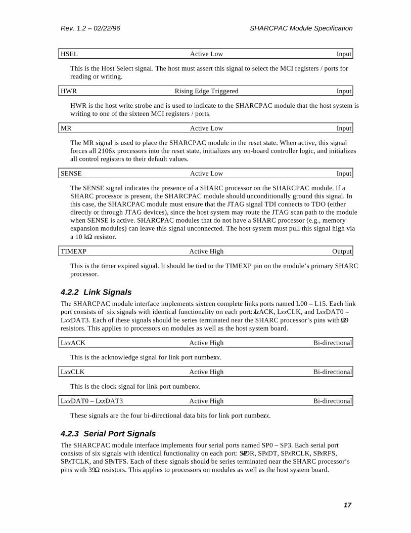
HSEL Active Low Input
This is the Host Select signal. The host must assert this signal to select the MCI registers / ports forreading or writing.
HWR Rising Edge Triggered Input
HWR is the host write strobe and is used to indicate to the SHARCPAC module that the host system iswriting to one of the sixteen MCI registers / ports.
MR Active Low Input
The MR signal is used to place the SHARCPAC module in the reset state. When active, this signalforces all 2106x processors into the reset state, initializes any on-board controller logic, and initializesall control registers to their default values.
SENSE Active Low Input
The SENSE signal indicates the presence of a SHARC processor on the SHARCPAC module. If aSHARC processor is present, the SHARCPAC module should unconditionally ground this signal. Inthis case, the SHARCPAC module must ensure that the JTAG signal TDI connects to TDO (eitherdirectly or through JTAG devices), since the host system may route the JTAG scan path to the modulewhen SENSE is active. SHARCPAC modules that do not have a SHARC processor (e.g., memoryexpansion modules) can leave this signal unconnected. The host system must pull this signal high viaa 10 kΩ resistor.
TIMEXP Active High Output
This is the timer expired signal. It should be tied to the TIMEXP pin on the module’s primary SHARCprocessor.
4.2.2 Link SignalsThe SHARCPAC module interface implements sixteen complete links ports named L00 – L15. Each linkport consists of six signals with identical functionality on each port: LxxACK, LxxCLK, and LxxDAT0 –LxxDAT3. Each of these signals should be series terminated near the SHARC processor’s pins with 39Ωresistors. This applies to processors on modules as well as the host system board.
LxxACK Active High Bi-directional
This is the acknowledge signal for link port number xx.
LxxCLK Active High Bi-directional
This is the clock signal for link port number xx.
LxxDAT0 – LxxDAT3 Active High Bi-directional
These signals are the four bi-directional data bits for link port number xx.
4.2.3 Serial Port SignalsThe SHARCPAC module interface implements four serial ports named SP0 – SP3. Each serial portconsists of six signals with identical functionality on each port: SPxDR, SPxDT, SPxRCLK, SPxRFS,SPxTCLK, and SPxTFS. Each of these signals should be series terminated near the SHARC processor’spins with 39Ω resistors. This applies to processors on modules as well as the host system board.

SHARCPAC Module Specification Rev. 1.2 – 02/22/96
18
SPxDR Active High Input
This is the data receive signal of serial port number x.
SPxDT Active High Output
This is the data transmit signal of serial port number x.
SPxRCLK Active High Bi-directional
This is the receive clock signal of serial port number x.
SPxRFS Active High Bi-directional
This is the receive frame sync signal of serial port number x.
SPxTCLK Active High Bi-directional
This is the transmit clock signal of serial port number x.
SPxTFS Active High Bi-directional
This is the transmit frame sync signal of serial port number x.
4.2.4 Flag SignalsFLAG0 – FLAG7 Active High Bi-directional
These signals are connected directly to the 2106x processors’ flag pins. Refer to section 2.6, ProcessorFlags for information regarding the connection of these signals to unidirectional devices.
4.2.5 Interrupt SignalsIRQ0 – IRQ7 Active Low or Falling Edge Triggered Input
These signals are connected directly to the interrupt request pins on the SHARCPAC module’sprocessors. Unused interrupt signals must be pulled high on the carrier board to prevent unintentionalinterrupts.
4.2.6 JTAG Emulation SignalsEMU Active Low Output
This is the JTAG emulation status signal.
ICSA Active Low Output
This is the JTAG in-circuit signal analysis signal. Its use is currently reserved and should not beconnected to any devices.
TCK Active High Input
This is the JTAG scan test clock signal that is generated by the host system and connected to all of theJTAG compatible devices on the SHARCPAC module that will participate in the JTAG boundary scanpath.

Rev. 1.2 – 02/22/96 SHARCPAC Module Specification
19
TDI Active High Input
This is the JTAG test data input signal which receives the boundary scan serial data. It should beconnected to the first JTAG compatible device on the SHARCPAC module that will participate in theJTAG boundary scan path. If no devices on the SHARCPAC module participate in the JTAG path, thissignal should be connected directly to TDO.
TDO Active High Output
This is the JTAG test data output signal which outputs the serial data from the last SHARCPACmodule device that is connected to the JTAG boundary scan path.
TMS Active Low Input
This is the JTAG test mode select signal. It should be connected to all of the JTAG compatible deviceson the SHARCPAC module that will participate in the JTAG boundary scan path.
TRST Active Low Input
This is the JTAG test reset signal that is generated by the host system and connected to all of theJTAG compatible devices on the SHARCPAC module that will participate in the JTAG boundary scanpath.
4.2.7 External Bus SignalsThe SHARCPAC module interface supports the following external bus signals to allow the host systemdirect access to external memory-mapped devices and the multiprocessor memory space of 2106xprocessors on the module. These signals can be directly connected to all devices in a shared cluster.
ACK Active High Bi-directional
This is the memory acknowledge signal.
ADDR00 – ADDR31 Active High Bi-directional
These are the thirty-two bus address signals.
ADRCLK Active High Bi-directional
This is the Address Clock signal for synchronous external memories.
BMS Active Low Bi-directional
This is the Boot Memory Select signal.
BR1 – BR6 Active Low Bi-directional
These are the six Multiprocessing Bus Request signals.
CPA Active Low Bi-directional
This is the Core Priority Access signal.
CS0 – CS5 Active Low Input
These are the six Chip Select signals that allow the host processor to select an 2106x processor.

SHARCPAC Module Specification Rev. 1.2 – 02/22/96
20
DATA00 – DATA47 Active High Bi-directional
These are the forty-eight bus data signals.
DMAG Active Low Bi-directional
This is the Direct Memory Access (DMA) Grant signal. It should be connected to the DMAG1* pin onall SHARC processors that are connected to the external bus.
DMAR Active Low Bi-directional
This is the DMA Request signal. It should be connected to the DMAR1* pin on all SHARC processorsthat are connected to the external bus.
HBG Active Low Bi-directional
This is the Host Bus Grant signal.
HBR Active Low Bi-directional
This is the Host Bus Request signal.
MS0 – MS3 Active Low Bi-directional
These are the four external memory bank select signals.
PAGE Active High Bi-directional
This is the DRAM page boundary signal.
RD Active Low Bi-directional
This is the memory read strobe signal.
REDY Active High Bi-directional
This is the Host Bus Acknowledge signal.
RPBA Active High Bi-directional
This is the Rotating Priority Bus Arbitration Select signal.
SBTS Active Low Bi-directional
This is the Suspend Bus Tristate signal.
SW Active Low Bi-directional
This is the synchronous write select signal.
WR Active Low Bi-directional
This is the memory write strobe signal.

Rev. 1.2 – 02/22/96 SHARCPAC Module Specification
21
4.2.8 Power/Ground SignalsVDD Power
These twenty signals supply the external power (nominally +5.0 VDC or +3.3 VDC) for the devices onthe SHARCPAC module.
GND Ground
These forty-five signals provide the external power supply return for the devices powered by the VDDsignals.
4.3 CLOCK DISTRIBUTION AND TERMINATION
A SHARCPAC module is provided with three clock lines that are driven by the host carrier board. Allthree lines should be driven independently and exactly in phase with the same clock signal that drivesSHARC processors on the carrier board. Multiprocessor SHARC designs require clock skew of <1nS. Tominimize skew between SHARC processors, the following rules should be adhered to:
1. Minimize clock trace length. Long traces increase delay to clock loads on that trace. This canlead to skew problems. Keep traces under six inches. Traces on the carrier board to theSHARCPAC interface should be especially short since the SHARCPAC module will haveadditional trace length on it.
2. Each clock trace should be end-terminated. The recommended termination is a seriescombination of a 50Ω resistor and a capacitor that brings the total load to 50pF.
3. Consider using an adjustable skew clock driver.
4.4 5V VS. 3.3VSince only one voltage is supplied to the SHARCPAC module, all of the components on a module shouldoperate at the same voltage level as the SHARC processor.
4.5 AC TIMING CHARACTERISTICS
The following sections detail the AC timing parameters for SHARCPAC module interfaces. Please notethat read and write timing are compatible with a 40 MHz SHARC processor operating with one wait state.
4.5.1 Reset TimingFigure 4-1 and Table 4-4 describe the timing parameters for the Master Reset (MR) signal and the BootMode Control (B0 - B1) signals.
Table 4-4 – Master Reset (MR) Timing Parameters
NameName DescriptionDescription MinMin MaxMax UnitUnittRP MR* pulse width 150 - nstBS B0/B1 setup to MR* inactive 50 - ns

SHARCPAC Module Specification Rev. 1.2 – 02/22/96
22
tRPtRPtBS
0ns 100ns
MR*
B0/B1
Figure 4-1 – Master Reset (MR) Timing Diagram
4.5.2 MCI Read TimingFigure 4-2 and Table 4-5 describe the timing parameters for the host system when it reads from theModule Control Interface.
Table 4-5 – MCI Read Timing Parameters
NameName DescriptionDescription MinMin MaxMax UnitUnittAS Address setup to HSEL* active 0 - nstAR Address setup to HRD* active 2 - nstAH Address hold from HRD* inactive 0 - nstSR HSEL* active to HRD* active 2 - nstRP HRD* pulse width 35 - nstDA Data access time from HRD* active - 30 nstDH Data hold time from HRD* inactive 0 - ns
tARtAS
tAH
tSR
tDAtRPtRP
tDH
0ns 50ns 100ns
HAx
HSEL*
HRD*
HDx
Figure 4-2 – MCI Read Timing Diagram

Rev. 1.2 – 02/22/96 SHARCPAC Module Specification
23
4.5.3 MCI Write TimingFigure 4-3 and Table 4-6 describe the timing parameters for the host system when it writes to the ModuleControl Interface.
Table 4-6 – MCI Write Timing Parameters
NameName DescriptionDescription MinMin MaxMax UnitUnittAS Address setup to HSEL* active 0 - nstAR Address setup to HWR* active 3 - nstAH Address hold from HWR* inactive 0 - nstSW HSEL* active to HWR* active 3 - nstWP HWR* pulse width 35 - nstDS Data setup time to HWR* inactive 30 - nstDH Data hold time from HWR* inactive 0 - ns
tAWtAS
tAH
tSW
tWPtDS tDH
tWP
0ns 50ns 100ns
HAx
HSEL*
HWR*
HDx
Figure 4-3 – MCI Write Timing Diagram

SHARCPAC Module Specification Rev. 1.2 – 02/22/96
24

Rev. 1.2 – 02/22/96 SHARCPAC Module Specification
25
5. MECHANICAL SPECIFICATIONSThis section specifies the dimensional requirements, pinout, and recommended connectors forSHARCPAC modules and carrier boards.
5.1 DIMENSIONS
5.1.1 Module DimensionsFigure 5-1 shows the dimensions for a SHARCPAC module. It shows the bottom side of the module (theside that faces the carrier board) and the mating connectors. The holes located at the corners are formounting purposes only and have no electrical connection.
Figure 5-1 – SHARCPAC Module Dimensions, Bottom View

SHARCPAC Module Specification Rev. 1.2 – 02/22/96
26
5.1.2 Module Site DimensionsFigure 5-2 shows the dimensions for a SHARCPAC site on a carrier board. As stated above, the holeslocated at the corners are for mounting purposes only and have no electrical connection.
Figure 5-2 – SHARCPAC Carrier Site Dimensions, Top View
5.1.3 Module Site SpacingSpecifications are being considered for a double-wide module that spans two module sites. Contact thepublisher of this document for the latest information regarding module site spacing.
5.1.4 Mating DimensionsFigure 5-3 shows the side view of a SHARCPAC module mounted on a carrier board. The connectors onthe carrier board have a fixed height; the connectors on the SHARCPAC module are available in multipleheights. Since components may be placed in the area below the SHARCPAC module, the module designershould chose the appropriate connector height to allow for adequate clearance for components installed onthe bottom side of the module.
Figure 5-3 – Mated SHARCPAC Dimensions, Side View

Rev. 1.2 – 02/22/96 SHARCPAC Module Specification
27
Table 5-1 – Mated SHARCPAC Dimensions
Label Description DimensionA Module clearance B + 0.025 in.B Module connector height Available heights (in.):
0.225, 0.295, 0.365, 0.440C Maximum component height on carrier board 0.165 in.D Minimum clearance between components on
module and components on carrier board0.050 in.
5.2 RECOMMENDED CONNECTOR
Table 5-2 lists the connectors that should be used on the SHARCPAC module and carrier board. Theconnectors that mount on the carrier board are available in one height. The connectors that mount on theSHARCPAC module are available in various heights to accommodate components that are installed on thebottom side of the module.
Table 5-2 – Recommended Connectors
LocationLocation TypeType ManufacturerManufacturer Height (in.)Height (in.) Part NumberPart NumberCarrier Board (receptacle) Surface Mount Samtec — SFM-145-L2-S-D-LCSHARCPAC Module (pin) Surface Mount Samtec 0.225 TFM-145-02-S-D-LC
0.295 TFM-145-12-S-D-LC0.365 TFM-145-22-S-D-LC0.435 TFM-145-32-S-D-LC
5.3 PINOUT
The SHARCPAC module’s 360 signals are implemented with four 90-pin connectors referenced by thenames J1 - J4. The pins are numbered sequentially: J1 contains pins numbered 1-90, J2 contains the pinsnumbered 91-180, J3 contains pins numbered 181-270, and J4 contains the pins numbered 271-360. Thefollowing sections list the mapping between the signal names and the pin numbers alphabetically and thennumerically. An asterisk (*) following a signal name indicates that the signal is active low.

SHARCPAC Module Specification Rev. 1.2 – 02/22/96
28
5.3.1 Alphabetical ListPINPIN NAMENAME306 ACK99 ADDR00100 ADDR01101 ADDR02102 ADDR03103 ADDR04104 ADDR05105 ADDR06106 ADDR07108 ADDR08109 ADDR09110 ADDR10111 ADDR11112 ADDR12113 ADDR13114 ADDR14115 ADDR15117 ADDR16118 ADDR17119 ADDR18120 ADDR19121 ADDR20122 ADDR21123 ADDR22124 ADDR23126 ADDR24127 ADDR25128 ADDR26129 ADDR27130 ADDR28131 ADDR29132 ADDR30133 ADDR31299 ADRCLK210 B0223 B1349 BMS*217 BR1*218 BR2*307 BR3*308 BR4*215 BR5*216 BR6*222 CLKINA135 CLKINB
PINPIN NAMENAME294 CLKINC171 CPA*50 CS0*303 CS1*84 CS2*304 CS3*51 CS4*52 CS5*226 DATA00227 DATA01228 DATA02229 DATA03230 DATA04231 DATA05232 DATA06233 DATA07235 DATA08236 DATA09237 DATA10238 DATA11239 DATA12240 DATA13241 DATA14242 DATA15244 DATA16245 DATA17246 DATA18247 DATA19248 DATA20249 DATA21250 DATA22251 DATA23253 DATA24254 DATA25255 DATA26256 DATA27257 DATA28258 DATA29259 DATA30260 DATA31262 DATA32263 DATA33264 DATA34265 DATA35266 DATA36
PINPIN NAMENAME267 DATA37268 DATA38269 DATA39359 DATA40358 DATA41357 DATA42356 DATA43355 DATA44354 DATA45353 DATA46352 DATA47346 DMAG*81 DMAR*96 EMU*8 FLAG0
30 FLAG1287 FLAG2286 FLAG3139 FLAG4138 FLAG5311 FLAG6310 FLAG77 GND
29 GND38 GND45 GND48 GND71 GND76 GND83 GND116 GND136 GND156 GND163 GND178 GND187 GND205 GND220 GND224 GND234 GND252 GND261 GND277 GND293 GND298 GND
PINPIN NAMENAME300 GND309 GND314 GND328 GND343 GND345 GND347 GND348 GND360 GND22 GND53 GND134 GND149 GND180 GND195 GND243 GND270 GND285 GND290 GND329 GND350 GND198 HA0199 HA1200 HA2201 HA3211 HBG*179 HBR*63 HD064 HD165 HD266 HD367 HD468 HD569 HD670 HD754 HPROG055 HPROG156 HPROG257 HPROG358 HPROG459 HPROG560 HPROG661 HPROG7203 HRD*204 HSEL*

Rev. 1.2 – 02/22/96 SHARCPAC Module Specification
29
PINPIN NAMENAME202 HWR*97 ICSA*289 IRQ0288 IRQ1197 IRQ2196 IRQ346 IRQ447 IRQ5312 IRQ6313 IRQ79 L00ACK
10 L00CLK11 L00DAT012 L00DAT113 L00DAT214 L00DAT3192 L01ACK191 L01CLK280 L01DAT0279 L01DAT1190 L01DAT2189 L01DAT3157 L02ACK158 L02CLK159 L02DAT0160 L02DAT1161 L02DAT2162 L02DAT3327 L03ACK326 L03CLK325 L03DAT0324 L03DAT1323 L03DAT2322 L03DAT323 L04ACK24 L04CLK25 L04DAT026 L04DAT127 L04DAT228 L04DAT3276 L05ACK275 L05CLK186 L05DAT0185 L05DAT1274 L05DAT2
PINPIN NAMENAME273 L05DAT3164 L06ACK165 L06CLK166 L06DAT0167 L06DAT1168 L06DAT2169 L06DAT3320 L07ACK319 L07CLK318 L07DAT0317 L07DAT1316 L07DAT2315 L07DAT316 L08ACK17 L08CLK18 L08DAT019 L08DAT120 L08DAT221 L08DAT3184 L09ACK183 L09CLK272 L09DAT0271 L09DAT1182 L09DAT2181 L09DAT3150 L10ACK151 L10CLK152 L10DAT0153 L10DAT1154 L10DAT2155 L10DAT3335 L11ACK334 L11CLK333 L11DAT0332 L11DAT1331 L11DAT2330 L11DAT36 L12ACK5 L12CLK4 L12DAT03 L12DAT12 L12DAT21 L12DAT3
284 L13ACK283 L13CLK
PINPIN NAMENAME194 L13DAT0193 L13DAT1282 L13DAT2281 L13DAT3143 L14ACK144 L14CLK145 L14DAT0146 L14DAT1147 L14DAT2148 L14DAT3342 L15ACK341 L15CLK340 L15DAT0339 L15DAT1338 L15DAT2337 L15DAT3140 MR*41 MS0*42 MS1*43 MS2*44 MS3*305 PAGE214 RD*212 REDY219 RESERVED208 RESERVED291 RESERVED141 RPBA39 SBTS221 SENSE*33 SP0DR36 SP0DT32 SP0RCLK31 SP0RFS35 SP0TCLK34 SP0TFS206 SP1DR297 SP1DT302 SP1RCLK301 SP1RFS296 SP1TCLK207 SP1TFS174 SP2DR177 SP2DT173 SP2RCLK
PINPIN NAMENAME172 SP2RFS176 SP2TCLK175 SP2TFS87 SP3DR90 SP3DT86 SP3RCLK85 SP3RFS89 SP3TCLK88 SP3TFS40 SW*91 TCK93 TDI95 TDO137 TIMEXP92 TMS*94 TRST*72 User Defined73 User Defined74 User Defined75 User Defined77 User Defined78 User Defined79 User Defined80 User Defined15 VDD37 VDD82 VDD98 VDD107 VDD170 VDD188 VDD209 VDD278 VDD292 VDD295 VDD321 VDD351 VDD49 VDD62 VDD125 VDD142 VDD225 VDD336 VDD344 VDD213 WR*

SHARCPAC Module Specification Rev. 1.2 – 02/22/96
30
5.3.2 Numerical List
J1J1 J2J2PinPin NameName PinPin NameName PinPin NameName PinPin NameName1 L12DAT3 2 L12DAT2 91 TCK 92 TMS*3 L12DAT1 4 L12DAT0 93 TDI 94 TRST*5 L12CLK 6 L12ACK 95 TDO 96 EMU*7 GND 8 FLAG0 97 ICSA* 98 VDD9 L00ACK 10 L00CLK 99 ADDR00 100 ADDR0111 L00DAT0 12 L00DAT1 101 ADDR02 102 ADDR0313 L00DAT2 14 L00DAT3 103 ADDR04 104 ADDR0515 VDD 16 L08ACK 105 ADDR06 106 ADDR0717 L08CLK 18 L08DAT0 107 VDD 108 ADDR0819 L08DAT1 20 L08DAT2 109 ADDR09 110 ADDR1021 L08DAT3 22 GND 111 ADDR11 112 ADDR1223 L04ACK 24 L04CLK 113 ADDR13 114 ADDR1425 L04DAT0 26 L04DAT1 115 ADDR15 116 GND27 L04DAT2 28 L04DAT3 117 ADDR16 118 ADDR1729 GND 30 FLAG1 119 ADDR18 120 ADDR1931 SP0RFS 32 SP0RCLK 121 ADDR20 122 ADDR2133 SP0DR 34 SP0TFS 123 ADDR22 124 ADDR2335 SP0TCLK 36 SP0DT 125 VDD 126 ADDR2437 VDD 38 GND 127 ADDR25 128 ADDR2639 SBTS 40 SW* 129 ADDR27 130 ADDR2841 MS0* 42 MS1* 131 ADDR29 132 ADDR3043 MS2* 44 MS3* 133 ADDR31 134 GND45 GND 46 IRQ4 135 CLKINB 136 GND47 IRQ5 48 GND 137 TIMEXP 138 FLAG549 VDD 50 CS0* 139 FLAG4 140 MR*51 CS4* 52 CS5* 141 RPBA 142 VDD53 GND 54 HPROG0 143 L14ACK 144 L14CLK55 HPROG1 56 HPROG2 145 L14DAT0 146 L14DAT157 HPROG3 58 HPROG4 147 L14DAT2 148 L14DAT359 HPROG5 60 HPROG6 149 GND 150 L10ACK61 HPROG7 62 VDD 151 L10CLK 152 L10DAT063 HD0 64 HD1 153 L10DAT1 154 L10DAT265 HD2 66 HD3 155 L10DAT3 156 GND67 HD4 68 HD5 157 L02ACK 158 L02CLK69 HD6 70 HD7 159 L02DAT0 160 L02DAT171 GND 72 User Defined 161 L02DAT2 162 L02DAT373 User Defined 74 User Defined 163 GND 164 L06ACK75 User Defined 76 GND 165 L06CLK 166 L06DAT077 User Defined 78 User Defined 167 L06DAT1 168 L06DAT279 User Defined 80 User Defined 169 L06DAT3 170 VDD81 DMAR* 82 VDD 171 CPA* 172 SP2RFS83 GND 84 CS2* 173 SP2RCLK 174 SP2DR85 SP3RFS 86 SP3RCLK 175 SP2TFS 176 SP2TCLK87 SP3DR 88 SP3TFS 177 SP2DT 178 GND89 SP3TCLK 90 SP3DT 179 HBR* 180 GND

Rev. 1.2 – 02/22/96 SHARCPAC Module Specification
31
J3J3 J4J4PinPin NameName PinPin NameName PinPin NameName PinPin NameName181 L09DAT3 182 L09DAT2 271 L09DAT1 272 L09DAT0183 L09CLK 184 L09ACK 273 L05DAT3 274 L05DAT2185 L05DAT1 186 L05DAT0 275 L05CLK 276 L05ACK187 GND 188 VDD 277 GND 278 VDD189 L01DAT3 190 L01DAT2 279 L01DAT1 280 L01DAT0191 L01CLK 192 L01ACK 281 L13DAT3 282 L13DAT2193 L13DAT1 194 L13DAT0 283 L13CLK 284 L13ACK195 GND 196 IRQ3 285 GND 286 FLAG3197 IRQ2 198 HA0 287 FLAG2 288 IRQ1199 HA1 200 HA2 289 IRQ0 290 GND201 HA3 202 HWR* 291 RESERVED 292 VDD203 HRD* 204 HSEL* 293 GND 294 CLKINC205 GND 206 SP1DR 295 VDD 296 SP1TCLK207 SP1TFS 208 RESERVED 297 SP1DT 298 GND209 VDD 210 B0 299 ADRCLK 300 GND211 HBG* 212 REDY 301 SP1RFS 302 SP1RCLK213 WR* 214 RD* 303 CS1* 304 CS3*215 BR5* 216 BR6* 305 PAGE 306 ACK217 BR1* 218 BR2* 307 BR3* 308 BR4*219 RESERVED 220 GND 309 GND 310 FLAG7221 SENSE* 222 CLKINA 311 FLAG6 312 IRQ6223 B1 224 GND 313 IRQ7 314 GND225 VDD 226 DATA00 315 L07DAT3 316 L07DAT2227 DATA01 228 DATA02 317 L07DAT1 318 L07DAT0229 DATA03 230 DATA04 319 L07CLK 320 L07ACK231 DATA05 232 DATA06 321 VDD 322 L03DAT3233 DATA07 234 GND 323 L03DAT2 324 L03DAT1235 DATA08 236 DATA09 325 L03DAT0 326 L03CLK237 DATA10 238 DATA11 327 L03ACK 328 GND239 DATA12 240 DATA13 329 GND 330 L11DAT3241 DATA14 242 DATA15 331 L11DAT2 332 L11DAT1243 GND 244 DATA16 333 L11DAT0 334 L11CLK245 DATA17 246 DATA18 335 L11ACK 336 VDD247 DATA19 248 DATA20 337 L15DAT3 338 L15DAT2249 DATA21 250 DATA22 339 L15DAT1 340 L15DAT0251 DATA23 252 GND 341 L15CLK 342 L15ACK253 DATA24 254 DATA25 343 GND 344 VDD255 DATA26 256 DATA27 345 GND 346 DMAG*257 DATA28 258 DATA29 347 GND 348 GND259 DATA30 260 DATA31 349 BMS* 350 GND261 GND 262 DATA32 351 VDD 352 DATA47263 DATA33 264 DATA34 353 DATA46 354 DATA45265 DATA35 266 DATA36 355 DATA44 356 DATA43267 DATA37 268 DATA38 357 DATA42 358 DATA41269 DATA39 270 GND 359 DATA40 360 GND

SHARCPAC Module Specification Rev. 1.2 – 02/22/96
32

Rev. 1.2 – 02/22/96 SHARCPAC Module Specification
33
6. LIST OF MANUFACTURERSThe following is a complete list of third-party manufacturers that provide components and servicesrelevant to the SHARCPAC module.
Analog DevicesOne Technology WayPO Box 9106Norwood, MA 02062-9106(617) 329-4700
For Vendor Code information only, contact:
Len May(617) 461-4308E-mail: [email protected]
Analog Devices manufactures the ADSP-2106x SHARC processor and maintains the list of uniqueSHARCPAC manufacturer Vendor Codes.
National Semiconductor2900 Semiconductor DrivePO Box 58090Santa Clara, CA 95052-8090(408) 721-5000
National Semiconductor manufactures the NM93C42AL serial EEPROM.
SAMTEC IncorporatedPO Box 1147New Albany, IN 47151-1147(800) SAMTEC-9 (USA & Canada)(812) 944-6733
SAMTEC manufactures the connectors used to bring the external signals of the SHARCPAC module tothe host system board.

SHARCPAC Module Specification Rev. 1.2 – 02/22/96
34
Rev. 1.2 – 02/22/96 SHARCPAC Module Specification
35
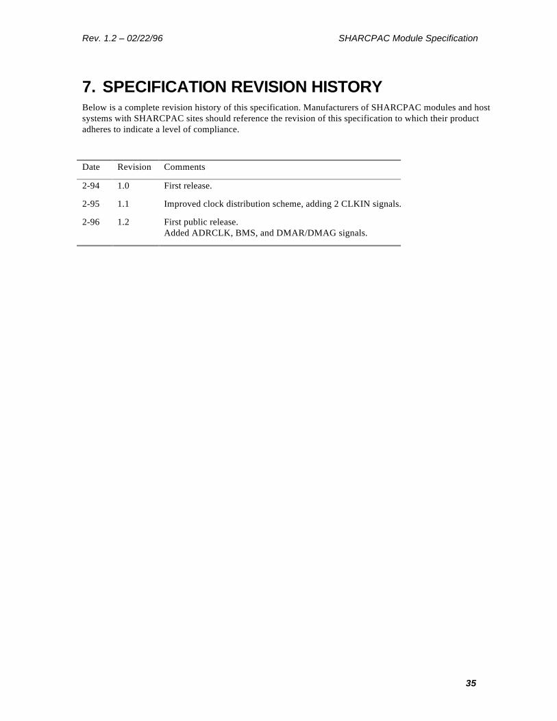
7. SPECIFICATION REVISION HISTORYBelow is a complete revision history of this specification. Manufacturers of SHARCPAC modules and hostsystems with SHARCPAC sites should reference the revision of this specification to which their productadheres to indicate a level of compliance.
Date Revision Comments
2-94 1.0 First release.
2-95 1.1 Improved clock distribution scheme, adding 2 CLKIN signals.
2-96 1.2 First public release.Added ADRCLK, BMS, and DMAR/DMAG signals.

SHARCPAC Module Specification Rev. 1.2 – 02/22/96
36