SFP Double Density 2X Pluggable Tranciver
107
Published Specifications SFP-DD/SFP-DD112/SFP112 Rev. 5.0 © SFP-DD MSA Page 1 October 1, 2021 1 2 3 SFP-DD MSA 4 5 SFP-DD/SFP-DD112/SFP112 Hardware Specification 6 7 for 8 9 SFP112 AND SFP DOUBLE DENSITY PLUGGABLE TRANSCEIVER 10 11 Revision 5.0 12 13 October 1, 2021 14 15 16 Abstract: This specification defines: the electrical and optical connectors, electrical signals and power supplies, 17 mechanical and thermal requirements of the pluggable SFP112 module, Double Density SFP-DD module, and 18 Double Density SFP-DD112 connector and cage system. This document provides a common specification for 19 systems manufacturers, system integrators, and suppliers of modules. 20 21 22 23 24 POINTS OF CONTACT: 25 Ali Ghiasi (Technical Editor) Ghiasi Quantum 19947 Lindenbrook Lane Cupertino, CA 95014 ali at ghiasiquantum dot com Scott Sommers (Chair) Molex 2222 Wellington Court Lisle, IL 60532-1682 scott.sommers at molex dot com 26 27 Website: 28 www.sfp-dd.com 29 30 Limitation on use of Information: 31 This specification is provided "AS IS" with NO WARRANTIES whatsoever and therefore the provision of this 32 specification does not include any warranty of merchantability, noninfringement, fitness for a particular 33 purpose, or any other warranty otherwise arising out of any proposal, specification or sample. The authors 34 further disclaim all liability, including liability for infringement of any proprietary rights, relating to use of 35 information in this specification. No license, express or implied, by estoppel or otherwise, to any intellectual 36 property rights is granted herein. 37 38 Permissions: 39 You are authorized to download, reproduce and distribute this document. All other rights are reserved. The 40 provision of this document should not be construed as the granting of any right to practice, make, use or 41 otherwise develop products that are based on the document. Any and all IP rights related to this document 42 and the designs disclosed within, except for the rights expressly mentioned above, are reserved by the 43 respective owners of those IP rights. 44 45 46
Transcript of SFP Double Density 2X Pluggable Tranciver

Published Specifications SFP-DD/SFP-DD112/SFP112 Rev. 5.0
© SFP-DD MSA Page 1 October 1, 2021
1 2 3
SFP-DD MSA 4
5
SFP-DD/SFP-DD112/SFP112 Hardware Specification 6
7
for 8
9
SFP112 AND SFP DOUBLE DENSITY PLUGGABLE TRANSCEIVER 10
11
Revision 5.0 12 13
October 1, 2021 14 15 16 Abstract: This specification defines: the electrical and optical connectors, electrical signals and power supplies, 17 mechanical and thermal requirements of the pluggable SFP112 module, Double Density SFP-DD module, and 18 Double Density SFP-DD112 connector and cage system. This document provides a common specification for 19 systems manufacturers, system integrators, and suppliers of modules. 20 21 22 23 24 POINTS OF CONTACT: 25 Ali Ghiasi (Technical Editor) Ghiasi Quantum 19947 Lindenbrook Lane Cupertino, CA 95014 ali at ghiasiquantum dot com
Scott Sommers (Chair) Molex 2222 Wellington Court Lisle, IL 60532-1682 scott.sommers at molex dot com
26 27 Website: 28 www.sfp-dd.com 29 30 Limitation on use of Information: 31 This specification is provided "AS IS" with NO WARRANTIES whatsoever and therefore the provision of this 32 specification does not include any warranty of merchantability, noninfringement, fitness for a particular 33 purpose, or any other warranty otherwise arising out of any proposal, specification or sample. The authors 34 further disclaim all liability, including liability for infringement of any proprietary rights, relating to use of 35 information in this specification. No license, express or implied, by estoppel or otherwise, to any intellectual 36 property rights is granted herein. 37 38 Permissions: 39 You are authorized to download, reproduce and distribute this document. All other rights are reserved. The 40 provision of this document should not be construed as the granting of any right to practice, make, use or 41 otherwise develop products that are based on the document. Any and all IP rights related to this document 42 and the designs disclosed within, except for the rights expressly mentioned above, are reserved by the 43 respective owners of those IP rights. 44 45 46

Published Specifications SFP-DD/SFP-DD112/SFP112 Rev. 5.0
© SFP-DD MSA Page 2 October 1, 2021
The following are Promoter member companies of the SFP-DD MSA. 1
Alibaba Group Hewlett Packard Enterprise Lumentum
Broadcom Huawei Molex
Cisco Intel TE Connectivity
Dell Technologies Juniper Networks
II-VI Nvidia
2 3 The following are Contributor member companies of the SFP-DD MSA. 4
Accelink Genesis Connected Solutions Nokia
Amphenol Hisense Broadband Senko
AOI Infinera Source Photonics
Eoptolink InnoLight US Conec
Foxconn Interconnect Technology Maxim Integrated Yamaichi Electronics
Fourte International MultiLane ZTE
5 6 Change History: 7
Revision Date Changes
1.0 September 14 2017 1st public release.
2.0 September 17, 2018 2nd public release. Added Type 2 module. Changed IntL pin to reserved, Changed TxFault to TxFault/Int Updated drawings to include new key. Added test conditions for insertion removal forces.
3.0 April 10 2019 3rd public release. Added 5 W power class. Added SN, MDC connectors. Deleted requirement that host shall not change the state of LPMode when module is present.
4.0 Withdrawn
4.1 August 10, 2020 4th public release. Added ResetL, IntL, ePPS, Fault signals. Added timing tables for low speeds signals, soft control and status. Chapter 7-Management Interface is now part of Chapter 4-Electrical Specification. Port mapping, optical connectors, and module color coding moved out of Mechanical and Board Definition Chapter-5 and into a new Chapter-5. Appendix A- Normative Connector Performance Requirements added.
4.2 August 17, 2020 5th public release. Added dual functionality IntL/TXFaultDD signal definition for SFP-DD.
5.0 October 1, 2021 Added chapter 5 Electrical Specifications for SFP112, added chapter 8 Mechanical specification of SFP-DD112, added chapter 9 Mechanical Specification of SFP112. Added ePPS/Clock signals definition for SFP-DD/SFP-DD112.
8 9 Foreword 10 The development work on this specification was done by the SFP-DD MSA, an industry group. The 11 membership of the committee since its formation in May 2017 has included a mix of companies which are 12 leaders across the industry. 13 14 The members of the SFP-DD MSA would like to acknowledge the contributions of Edmund Poh. He was an 15 excellent engineer; his technical skills and collaborative attitude will be missed. 16 17 18

Published Specifications SFP-DD/SFP-DD112/SFP112 Rev. 5.0
© SFP-DD MSA Page 3 October 1, 2021
TABLE OF CONTENTS 1 2
1. Scope .............................................................................................................................................................................. 9 3
1.1 Overview of SFP-DD/SFP-DD112/SFP112 Specifications .................................................................................... 9 4
2. References.................................................................................................................................................................... 10 5
2.1 Industry Documents .............................................................................................................................................. 10 6 2.2 SFF Specifications: ............................................................................................................................................... 10 7 2.3 Sources ................................................................................................................................................................. 10 8
3. Introduction ................................................................................................................................................................... 11 9
3.1 Objectives ............................................................................................................................................................. 11 10 3.2 SFP-DD/SFP-DD112/SFP112 System Overview................................................................................................. 11 11 3.3 Applications........................................................................................................................................................... 13 12
4. Electrical Specification and Management Interface Timing for SFP-DD/SFP-DD112 ................................................. 14 13
4.1 General Requirements .......................................................................................................................................... 14 14 4.2 Electrical Connector .............................................................................................................................................. 14 15 4.3 Overview of the Low Speed Electrical Hardware Signals .................................................................................... 17 16
4.3.1 TxDisable, TxDisableDD............................................................................................................................... 17 17 4.3.2 RxLOS, RxLOSDD ....................................................................................................................................... 17 18 4.3.3 Speed1, Speed2, Speed1DD, Speed2DD ................................................................................................... 17 19 4.3.4 TxFault .......................................................................................................................................................... 17 20 4.3.5 IntL/TxFaultDD .............................................................................................................................................. 18 21 4.3.6 Mod_ABS ...................................................................................................................................................... 18 22 4.3.7 LPMode ......................................................................................................................................................... 18 23 4.3.8 ResetL ........................................................................................................................................................... 18 24 4.3.9 ePPS/Clock PTP Reference Clock (Optional) .............................................................................................. 18 25 4.3.10 TWI Signals SCL, SDA ................................................................................................................................. 19 26
4.4 Example SFP-DD/SFP-DD112 Host Board Schematics ...................................................................................... 19 27 4.5 Low Speed Electrical Specification ....................................................................................................................... 23 28
4.5.1 TWI Logic Levels and Bus Loading .............................................................................................................. 23 29 4.6 Management Interface and Timing ....................................................................................................................... 24 30
4.6.1 Management Timing Specification ............................................................................................................... 25 31 4.6.1.1 Bus timing tBUF ........................................................................................................................................................................... 26 32 4.6.1.2 Bus timing tWR ............................................................................................................................................................................ 26 33 4.6.1.3 Bus timing tNACK ........................................................................................................................................................................ 27 34 4.6.1.4 Bus timing tBPC ........................................................................................................................................................................... 28 35
4.7 Timing for soft control and status functions .......................................................................................................... 29 36 4.8 High Speed Electrical Specifications .................................................................................................................... 30 37
4.8.1 RD0+, RD0-, RD1+, RD1- ............................................................................................................................ 30 38 4.8.2 TD0+, TD0-, TD1+, TD1- .............................................................................................................................. 31 39
4.9 Rate Select Hardware Control .............................................................................................................................. 31 40 4.10 Power Requirements ............................................................................................................................................ 32 41
4.10.1 Power Classes and Maximum Power Consumption .................................................................................... 32 42 4.10.2 Host Board Power Supply Filtering ............................................................................................................... 33 43 4.10.3 Module Power Supply Specification ............................................................................................................. 33 44 4.10.4 Host Board Power Supply Noise Output ...................................................................................................... 35 45 4.10.5 Module Power Supply Noise Output............................................................................................................. 36 46 4.10.6 Module Power Supply Noise Tolerance ....................................................................................................... 36 47
4.11 ESD ....................................................................................................................................................................... 37 48
5. Electrical Specification and Management Interface Timing for SFP112 ...................................................................... 38 49
5.1 General Requirements .......................................................................................................................................... 38 50 5.2 SFP112 Electrical Connector ............................................................................................................................... 38 51 5.3 Overview of the Low Speed Electrical Hardware Signals .................................................................................... 40 52
5.3.1 TxDisable ...................................................................................................................................................... 40 53 5.3.2 RxLOS .......................................................................................................................................................... 41 54 5.3.3 Speed1, Speed2 ........................................................................................................................................... 41 55

Published Specifications SFP-DD/SFP-DD112/SFP112 Rev. 5.0
© SFP-DD MSA Page 4 October 1, 2021
5.3.4 TxFault/IntL ................................................................................................................................................... 41 1 5.3.5 Mod_ABS ...................................................................................................................................................... 41 2 5.3.6 TWI Signals SCL, SDA ................................................................................................................................. 41 3
5.4 Example SFP112 Host Board Schematics ........................................................................................................... 41 4 5.5 Low Speed Electrical Specification ....................................................................................................................... 44 5
5.5.1 TWI Logic Levels and Bus Loading .............................................................................................................. 45 6 5.6 Management Interface and Timing ....................................................................................................................... 46 7
5.6.1 Management Timing Specification ............................................................................................................... 47 8 5.6.1.1 Bus timing tBUF ........................................................................................................................................................................... 48 9 5.6.1.2 Bus timing tWR ............................................................................................................................................................................ 48 10 5.6.1.3 Bus timing tNACK ........................................................................................................................................................................ 49 11 5.6.1.4 Bus timing tBPC ........................................................................................................................................................................... 50 12
5.7 Timing for soft control and status functions .......................................................................................................... 51 13 5.8 High Speed Electrical Specifications .................................................................................................................... 52 14
5.8.1 RD0+, RD0- .................................................................................................................................................. 52 15 5.8.2 TD0+, TD0- ................................................................................................................................................... 53 16
5.9 Rate Select Hardware Control .............................................................................................................................. 53 17 5.10 Power Requirements ............................................................................................................................................ 54 18
5.10.1 Power Classes and Maximum Power Consumption .................................................................................... 54 19 5.10.2 Host Board Power Supply Filtering ............................................................................................................... 55 20 5.10.3 Module Power Supply Specification ............................................................................................................. 55 21 5.10.4 Host Board Power Supply Noise Output ...................................................................................................... 57 22 5.10.5 Module Power Supply Noise Output............................................................................................................. 58 23 5.10.6 Module Power Supply Noise Tolerance ....................................................................................................... 58 24
5.11 ESD ....................................................................................................................................................................... 59 25
6. Optical Port Mapping and Optical Interfaces ................................................................................................................ 60 26
6.1 Electrical data input/output to optical port mapping.............................................................................................. 60 27 6.2 Optical Interfaces .................................................................................................................................................. 60 28
6.2.1 MPO Optical Cable connections ................................................................................................................... 61 29 6.2.2 Duplex LC Optical Cable connection ............................................................................................................ 61 30 6.2.3 SN Optical Cable connections ...................................................................................................................... 62 31 6.2.4 MDC Optical Cable connections ................................................................................................................... 63 32
6.3 Module Color Coding and Labeling ...................................................................................................................... 63 33
7. SFP-DD Mechanical and Board Definition ................................................................................................................... 64 34
7.1 Introduction to SFP-DD and SFP-DD112 ............................................................................................................. 64 35 7.2 SFP-DD/SFP-DD112/SFP112 Datums, Dimensions and Component Alignment ............................................... 66 36 7.3 SFP-DD Cage, Connector, Module Alignment ..................................................................................................... 67 37 7.4 SFP-DD/SFP-DD112 Module Mechanical Dimensions ........................................................................................ 68 38 7.5 SFP-DD/SFP-DD112/SFP112 Module Flatness and Roughness ........................................................................ 72 39 7.6 SFP-DD Module paddle card dimensions ............................................................................................................ 72 40 7.7 SFP-DD/SFP-DD112/SFP112 Module Extraction and Retention Forces ............................................................ 75 41 7.8 Press fit Cage Mechanical .................................................................................................................................... 75 42 7.9 SMT Electrical Connector Mechanical.................................................................................................................. 81 43
7.9.1 SMT connector and cage host PCB layout .................................................................................................. 84 44
8. SFP-DD112 Mechanical and Board Definition ............................................................................................................. 86 45
8.1 Introduction ........................................................................................................................................................... 86 46 8.2 SFP-DD112 module mechanical dimensions ....................................................................................................... 86 47 8.3 SFP-DD112 Improved Module paddle card dimensions ...................................................................................... 87 48 8.4 Press fit Cage Mechanical .................................................................................................................................... 90 49 8.5 SMT Electrical Connector Mechanical.................................................................................................................. 91 50
8.5.1 SMT connector and cage host PCB layout .................................................................................................. 93 51
9. SFP112 Mechanical and Board Definition .................................................................................................................... 95 52
9.1 Introduction ........................................................................................................................................................... 95 53 9.2 SFP112 Datum for Module, Cage, Connector and Host ...................................................................................... 95 54 9.3 SFP112 Cage, Connector, Module Alignment ..................................................................................................... 96 55 9.4 SFP112 module mechanical dimensions ............................................................................................................. 97 56
Published Specifications SFP-DD/SFP-DD112/SFP112 Rev. 5.0
© SFP-DD MSA Page 5 October 1, 2021
9.5 SFP112 Improved Module paddle card dimensions............................................................................................. 99 1 9.6 SFP112 SMT Electrical Connector ..................................................................................................................... 100 2
9.6.1 SFP112 SMT host PCB layout ................................................................................................................... 101 3
10. Environmental and Thermal........................................................................................................................................ 103 4
10.1 Thermal Requirements ....................................................................................................................................... 103 5
Appendix A Normative Module and Connector Performance Requirements ................................................................ 104 6
A.1 Performance Tables ........................................................................................................................................... 104 7 8 9 10

Published Specifications SFP-DD/SFP-DD112/SFP112 Rev. 5.0
© SFP-DD MSA Page 6 October 1, 2021
List of Tables 1
2 Table 1- Pad Function Definition .......................................................................................................................................... 16 3 Table 2- ePPS/Clock Advertising Capabilities ...................................................................................................................... 19 4 Table 3- ePPS or Clock Modes ............................................................................................................................................ 19 5 Table 4- ePPS or Clock Frequency ...................................................................................................................................... 19 6 Table 5- Low Speed Control and Sense Signals.................................................................................................................. 23 7 Table 6- Management Interface timing parameters ............................................................................................................. 26 8 Table 7- Timing for SFP-DD/SFP-DD112 soft control and status functions ........................................................................ 29 9 Table 8- I/O Timing for Squelch & Disable ........................................................................................................................... 30 10 Table 9- Rate Select Hardware Control................................................................................................................................ 31 11 Table 10- Power Classification ............................................................................................................................................. 32 12 Table 11- Power Supply specifications, Instantaneous, sustained and steady state current limits ..................................... 34 13 Table 12- Truncated Filter Response Coefficients for Host Power Supply Noise Output.................................................... 35 14 Table 13- Power Supply Output Noise and Tolerance Specifications ................................................................................. 36 15 Table 14- Pad Function Definition ........................................................................................................................................ 40 16 Table 15- Low Speed Control and Sense Signals................................................................................................................ 45 17 Table 16- Management Interface timing parameters ........................................................................................................... 48 18 Table 17- Timing for SFP-DD/SFP-DD112 soft control and status functions ...................................................................... 51 19 Table 18- I/O Timing for Squelch & Disable ......................................................................................................................... 52 20 Table 19- Rate Select Hardware Control.............................................................................................................................. 53 21 Table 20- Power Classification ............................................................................................................................................. 54 22 Table 21- Power Supply specifications, Instantaneous, sustained and steady state current limits ..................................... 56 23 Table 22- Truncated Filter Response Coefficients for Host Power Supply Noise Output.................................................... 57 24 Table 23- Power Supply Output Noise and Tolerance Specifications ................................................................................. 58 25 Table 24- Electrical data input to Optical Port Mapping ....................................................................................................... 60 26 Table 25- Datum Description ................................................................................................................................................ 66 27 Table 26- Module flatness specifications.............................................................................................................................. 72 28 Table 27: SFP112 Datum ..................................................................................................................................................... 95 29 Table 28- Temperature Range Class of operation ............................................................................................................. 103 30 Table 29- Form Factor Performance Requirements........................................................................................................... 104 31 Table 30- EIA-364-1000 Test Details ................................................................................................................................. 105 32 Table 31- Additional Test Procedures ................................................................................................................................ 106 33 34
35

Published Specifications SFP-DD/SFP-DD112/SFP112 Rev. 5.0
© SFP-DD MSA Page 7 October 1, 2021
List of Figures 1 2
Figure 1: Application Reference Model ................................................................................................................................ 13 3 Figure 2: SFP-DD/SFP-DD112/SFP112 Cage, Connector and Module .............................................................................. 13 4 Figure 3: SFP-DD/SFP-DD112 module pad layout .............................................................................................................. 15 5 Figure 4: Example SFP-DD/SFP-DD112 Host Board Schematic for Optical Modules ........................................................ 20 6 Figure 5: Example SFP-DD/SFP-DD112 Host Board Schematic for active copper cables ................................................. 21 7 Figure 6: Example SFP-DD/SFP-DD112 Host Board Schematic for passive copper cables .............................................. 22 8 Figure 7: SDA/SCL options for pull-up resistor, bus capacitance and rise/fall times ........................................................... 24 9 Figure 8: SFP-DD/SFP-DD112 Two Wire Interface Timing ................................................................................................. 25 10 Figure 9: Bus timing tWR ...................................................................................................................................................... 27 11 Figure 10: Bus timing tNACK ................................................................................................................................................ 27 12 Figure 11: Bus timing tBPC .................................................................................................................................................. 28 13 Figure 12: Recommended Host Board Power Supply Filtering............................................................................................ 33 14 Figure 13: Instantaneous and sustained peak currents for Icc Host (see Table 11) ........................................................... 35 15 Figure 14: Truncated Transfer Response for Host Board Power Supply Noise Output measurement ............................... 36 16 Figure 15: Module Noise Injection Point ............................................................................................................................... 37 17 Figure 16: SFP112 module pad layout ................................................................................................................................. 39 18 Figure 17: Example of SFP112 Host Board Schematic for Optical Modules ....................................................................... 42 19 Figure 18: Example of SFP112 Host Board Schematic for active copper cables ................................................................ 43 20 Figure 19: Example of SFP112 Host Board Schematic for passive copper cables ............................................................. 44 21 Figure 20: SDA/SCL options for pull-up resistor, bus capacitance and rise/fall times ......................................................... 46 22 Figure 21: SFP112 Two Wire Interface Timing .................................................................................................................... 47 23 Figure 22: Bus timing tWR .................................................................................................................................................... 49 24 Figure 23: Bus timing tNACK ................................................................................................................................................ 49 25 Figure 24: Bus timing tBPC .................................................................................................................................................. 50 26 Figure 25: SFP112 Recommended Host Board Power Supply Filtering ............................................................................. 55 27 Figure 26: Instantaneous and sustained peak currents for Icc Host (see Table 21) ........................................................... 57 28 Figure 27: Truncated Transfer Response for Host Board Power Supply Noise Output measurement ............................... 58 29 Figure 28: Module Noise Injection Point ............................................................................................................................... 59 30 Figure 29: Optical Media Dependent Interface port assignments ........................................................................................ 60 31 Figure 30: MPO-12 Single Row optical patch cord and module receptacle......................................................................... 61 32 Figure 31: Duplex LC optical patchcord and module receptacle.......................................................................................... 61 33 Figure 32: LC connector excursion above module nose height ........................................................................................... 62 34 Figure 33: Minimum vertical port pitch.................................................................................................................................. 62 35 Figure 34: SN optical connector plug and two-port module receptacle ............................................................................... 62 36 Figure 35: MDC optical connector plug and two-port module receptacle ............................................................................ 63 37 Figure 36: Press fit cage ....................................................................................................................................................... 64 38 Figure 37: SFP-DD and SFP-DD112 Modules ..................................................................................................................... 65 39 Figure 38: Cage, Connector alignment................................................................................................................................. 67 40 Figure 39: Type 1 and Type 2 Modules ................................................................................................................................ 68 41 Figure 40: Detailed dimensions of module ........................................................................................................................... 71 42 Figure 41: Module paddle card dimensions ......................................................................................................................... 73 43 Figure 42: Module pad dimensions ...................................................................................................................................... 74 44 Figure 43: Press Fit 1x1 Cage .............................................................................................................................................. 75 45 Figure 44: Press Fit 1x1 Cage Design.................................................................................................................................. 78 46 Figure 45: Press Fit Cage Detail .......................................................................................................................................... 79 47 Figure 46: 1 x n bezel opening ............................................................................................................................................. 80 48 Figure 47: SMT connector .................................................................................................................................................... 81 49 Figure 48: 1x1 Connector Design and Host PCB Pin Numbers ........................................................................................... 83 50 Figure 49: Host PCB Mechanical Layout.............................................................................................................................. 85 51 Figure 50: SFP-DD112 Module Bottom View Details ........................................................................................................... 86 52 Figure 51: Improved module paddle card dimensions ......................................................................................................... 88 53 Figure 52: Improved module pad dimensions ...................................................................................................................... 89 54 Figure 53: Press Fit 1x1 Cage .............................................................................................................................................. 90 55 Figure 54: SMT connector .................................................................................................................................................... 91 56 Figure 55: 1x1 Connector Design and Host PCB Pin Numbers ........................................................................................... 92 57 Figure 56: Host PCB Mechanical Layout.............................................................................................................................. 94 58 Figure 57: SFP112 1x1 Cage and Host PCB Layout ........................................................................................................... 96 59 Figure 58: SFP112 High Speed Pads Viewing Windows ..................................................................................................... 98 60

Published Specifications SFP-DD/SFP-DD112/SFP112 Rev. 5.0
© SFP-DD MSA Page 8 October 1, 2021
Figure 59: SFP112 improved module paddle card dimensions ........................................................................................... 99 1 Figure 60: SFP112 SMT Connector ................................................................................................................................... 100 2 Figure 61: SFP112 Host Pad Layout .................................................................................................................................. 101 3 Figure 62: SFP112 Detailed Host Pad Layout ................................................................................................................... 102 4 Figure 63: 1x1 Connector Design and Host PCB Pad Numbers........................................................................................ 102 5 6

Published Specifications SFP-DD/SFP-DD112/SFP112 Rev. 5.0
© SFP-DD MSA Page 9 October 1, 2021
1. Scope 1
The scope of this specification is the definition of a high density 1-channel and 2-channels modules, cage and 2 connector system. SFP-DD supports up to 100 Gb/s in aggregate over a 2 x 50Gb/s electrical interface. 3 SFP112 supports 100 Gb/s over single electrical lane, and SFP-DD112 supports up to 200 Gb/s in aggregate 4 over a 2 x 100 Gb/s electrical interface. The cage and connector design provides backwards compatibility to 5 SFP+/SFP28 [30], [28] modules which can be inserted into an SFP-DD/SFP-DD112 cage and connector using 6 1 of the electrical channels. SFP112 cage and connectors are compatible with SFP+/SFP28 modules. 7 Furthermore, SFP112 modules maybe inserted into SFP-DD112 cage and connector using 1 of the electrical 8 lanes. 9 10
1.1 Overview of SFP-DD/SFP-DD112/SFP112 Specifications 11
SFP-DD/SFP-DD112/SFP112 specifications are organized into 10 chapters and one appendix addressing electrical, 12 mechanical, environmental, and management aspects of the module. 13
14 • Chapter 1 Scope 15
16 • Chapter 2 References and Related Standards and SFF Specifications 17
18 • Chapter 3 Introduction 19
20 • Chapter 4 Electrical specifications and management interface timing for SFP-DD/SFP-DD112 21
22 • Chapter 5 Electrical specifications and management interface timing for SFP112 23
24 • Chapter 6 Optical port mapping and optical interfaces 25
26 • Chapter 7 SFP-DD Mechanical specifications, printed circuit board recommendations 27
28 • Chapter 8 SFP-DD112 Mechanical specifications, printed circuit board recommendations 29
30 • Chapter 9 SFP112 Mechanical specifications, printed circuit board recommendations 31
32 • Chapter 10 Environmental and thermal considerations 33
34 • Appendix A Normative module and connector performance requirements. 35
36 37

Published Specifications SFP-DD/SFP-DD112/SFP112 Rev. 5.0
© SFP-DD MSA Page 10 October 1, 2021
2. References 1
2.1 Industry Documents 2
The following interface standards and specifications are relevant to this Specification. 3
[1] ANSI FC-PI-6 32GFC (INCITS 533) 4
[2] ANSI FC-PI-7 64GFC (INCITS 543) 5
[3] ANSI FC-PI-8 128GFC 6
[4] ASME Y14.5-2009 Dimensioning and Tolerancing 7
[5] Common Management Interface Specification (CMIS) 5.0, see http://www.qsfp-dd.com 8
[6] CS-01242017 CS optical connector and receptacle, see http://www.qsfp-dd.com/optical-connector/ 9
[7] EIA-364-1000 TS-1000B Environmental Test Methodology for Assessing the Performance of Electrical 10
Connectors and Sockets Used in Controlled Environment Applications, revision B 2009 11
[8] EN6100-4-2 (IEC immunity standard on ESD), criterion B test specification 12
[9] Human Body Model per ANSI/ESDA/JEDEC JS-001 13
[10] IEC 61754-7-1 (Fibre Optic Interconnecting Devices and Passive Components - Fibre Optic Connector 14
Interfaces - Part 7-1: Type MPO Connector Family - One Fibre Row) 15
[11] IEC 61754-20 (Fibre Optic Interconnecting Devices and Passive Components - Fibre Optic Connector 16
Interfaces - Part 20: Type LC Connector Family) 17
[12] IEEE Std 802.3TM-2018, annex 86A, 83E, and 120E 18
[13] IEEE Std 802.3cd (50 Gb/s, 100 Gb/s, and 200 Gb/s Ethernet), clause 136 and annex 136A 19
[14] IEEE Std 802.3ck (100 Gb/s, 200 Gb/s, and 400 Gb/s Electrical Interfaces) 20
[15] IEEE Std 1588 Precision Clock Synchronization Protocol PTP, 2019 21
[16] InfiniBand Architecture Specification Volume 2 22
[17] JEDEC JESD8C.01 Interface Standard for Nominal 3.0/3.3 V Supply Digital Integrated Circuit (LVCMOS) 23
[18] NEBS GR-63 Physical Protection Requirements for Network Telecommunications Equipment 24
[19] NXP UM10204, I2C-bus specification and user manual, Rev 6 – 4 April 2014. 25
[20] OIF CEI 4.0, CL-13 CEI-28G-VSR, CL-16 CEI-56G-VSR PAM4, and CEI-112G-VSR PAM4 specifications 26
[21] SFP-DD Management Interface, Rev. 2.0 27
[22] SN-60092019 SN optical connector and receptacle, see http://www.qsfp-dd.com/optical-connector/ 28
[23] TIA-604-5 (FOCIS 5 Fiber Optic Connector Intermateability Standard- Type MPO) 29
[24] TIA-604-10 (FOCIS 10 Fiber Optic Connector Intermateability Standard- Type LC) 30
[25] USC-11383001 MDC optical plug and receptacle, see http://www.qsfp-dd.com/optical-connector/ 31
2.2 SFF Specifications: 32
[26] INF-8074i SFP (Small Formfactor Pluggable) Transceiver, Rev. 1.0 33
[27] SFF-8071 SFP+ 1x 0.8 mm Card Edge Connector, Rev 1.1 34
[28] SFF-8402 SFP+ 1x 28 Gb/s Pluggable Transceiver Solution (SFP28), Rev. 1.1 35
[29] SFF-8419 SFP+ Power and Low Speed Interface, Rev. 1.3 36
[30] SFF-8431 SFP+ 10 Gb/s and Low Speed Electrical Interface, Rev. 4.1 37
[31] SFF-8432 SFP+ Module and Cage, Rev. 5.2a 38
[32] SFF-8433 SFP+ Ganged Cage Footprints and Bezel Openings, Rev. 0.7 39
[33] SFF-8472 Diagnostic Monitoring Interface for Optical Transceivers, Rev. 12.4. 40 41
2.3 Sources 42
The SFP-DD MSA SFP-DD Hardware Specification for SFP DOUBLE DENSITY 2X PLUGGABLE 43 TRANSCEIVER can be obtained via the www.SFP-DD.com web site. 44 45

Published Specifications SFP-DD/SFP-DD112/SFP112 Rev. 5.0
© SFP-DD MSA Page 11 October 1, 2021
3. Introduction 1
2 This Specification covers the following items: 3 4
• Electrical interfaces including pad assignments for data, control, status and power supplies and host 5 PCB layout requirements. 6
7 • Optical interfaces (including optical receptacles and mating fiber plugs for multimode and single-mode 8
duplex and parallel fiber applications). Breakout cable applications are also specified. 9 10
• Mechanical specifications including dimensions and tolerances for the connector, cage and module 11 system. Includes details of the requirements for correct mating of the module and host sides of the 12 connector. 13
14 • Thermal requirements 15
16 • Management Interface Timing requirements 17
18 • Electrostatic discharge (ESD) requirements by reference to industry standard limits and test methods. 19
20 This Specification does not cover the following items: 21 22
• Electromagnetic interference (EMI) protection. EMI protection is the responsibility of the implementers 23 of the cages and modules. 24
25 • Optical signaling specifications are not included in this document but are defined in the applicable 26
industry standards. 27 28
• Management Registers. 29 30
3.1 Objectives 31
SFP-DD/SFP-DD112 electrical signals, channel assignments, TWI, timing, and power requirements are 32 defined in Chapter 4. SFP112 electrical signals, TWI, timing, and power requirements are defined in Chapter 33 5. Optical port mapping and optical interfaces are defined in Chapter 6 to ensure that the pluggable modules 34 and cable assemblies are functionally interchangeable. Implementations compliant to dimensions, mounting 35 and insertion requirements defined in Chapter 7 for SFP-DD bezel, optical module, cable plug, cage and 36 connector system on a circuit board ensure that these products are mechanically interchangeable. Chapter 8 37 describes an improved SFP-DD form factor called SFP-DD112 with improved signal integrity for 100 Gb/s per 38 lane operation with an aggregate bandwidth of 200 Gb/s. Chapter 9 describes an improved SFP+ form factor 39 called SFP112 with improved signal integrity for 100 Gb/s per lane operation and with an aggregate bandwidth 40 of 100 Gb/s. 41 42
3.2 SFP-DD/SFP-DD112/SFP112 System Overview 43
The SFP-DD form factor system consisting of a transceiver module, cage and connector provides two 44 channels for high speed signals that can support a two-lane trunked application or two independent single-lane 45 applications. The cage and socket can also accept SFP+/SFP28 and SFP112 modules in which case a single 46 lane channel is supported. To support classic SFP+ modules the electrical connector maintains the twenty 47 contacts row defined for SFP+ modules and adds another twenty contacts row to support a second channel. 48 49 In addition to contacts for the high speed data signals, the connector provides contacts for module and 50 channel control and status signals including a pair that form a Two-Wire Interface (TWI) [19] or communication 51 with the module's memory. Contacts for high speed data signals, channel level control and status indicator 52 signals and power supply sources for the SFP module are repeated in the row for the second channel. 53

Published Specifications SFP-DD/SFP-DD112/SFP112 Rev. 5.0
© SFP-DD MSA Page 12 October 1, 2021
Contacts for module level control and status signals in the SFP module remain in place and signals for new 1 module level functions were added to the second row. 2 3 New global features and associated signals, Low Power Mode, Reset and Interrupt were added and the 4 memory map for SFP-DD was expanded and reorganized for better alignment with CMIS functionality and 5 structure. 6 7 SFP-DD management specifications is based on SFP-DD MIS [21]. SFP-DD112 and SFP112 management 8 specifications are based on CMIS [5]. 9 10 Within the MIS and CMIS the SFP112 and SFP-DD/SFP-DD112 classic contacts, see Figure 3, are associated 11 as Channel 1 and the SFP-DD/SFP-DD112 additional contacts are associated as Channel 2. Within this 12 document the name, Channel 1, is synonymous with the name SFP “classic” Channel and Channel 2 is 13 synonymous with the name DD “additional” Channel. 14 15 Adding a second channel to SFP-DD/SFP-DD112 results in increased module power consumption. 16 Accommodations for the increased consumption include defining additional power classes, defining a Type 2 17 module and defining an enlarged heat sink seating area with surface flatness and roughness requirements. A 18 low power mode was added to provide the host a means for power management. 19 20 Another accommodation for a second channel was the inclusion of addition optical connectors including MPO 21 [10] and [23], duplex LC [11] and [24], see Figure 29. 22 23 24 25 26

Published Specifications SFP-DD/SFP-DD112/SFP112 Rev. 5.0
© SFP-DD MSA Page 13 October 1, 2021
3.3 Applications 1
2 This specification defines a connector, cage and module for single or double lane applications at up to 112 3 Gb/s (56 GBd) per lane. Intended applications include but are not limited to Ethernet and/or InfiniBand and/or 4 Fibre Channel. The SFP-DD/SFP-DD112/SFP112 interface can support pluggable modules or direct attach 5 cables based on multimode fiber, single mode fiber or copper wires. 6 7 An application reference Model, shown in Figure 1, shows the high-speed data interface between an ASIC and 8 the SFP-DD/SFP-DD112/SFP112 modules. 9
10
Figure 1: Application Reference Model 11 12
13 Figure 2: SFP-DD/SFP-DD112/SFP112 Cage, Connector and Module 14

Published Specifications SFP-DD/SFP-DD112/SFP112 Rev. 5.0
© SFP-DD MSA Page 14 October 1, 2021
4. Electrical Specification and Management Interface Timing for SFP-DD/SFP-DD112 1
2 This chapter contains signal definitions and requirements that are specific to the SFP-DD/SFP-DD112 3 modules. High-speed signal requirements including compliance points for electrical measurements are defined 4 in the applicable industry standard. 5 6
4.1 General Requirements 7
The SFP-DD/SFP-DD112 modules are hot-pluggable. Hot pluggable refers to plugging in or unplugging a 8 module while the host board is powered. 9 10 For EMI protection the signals from the host connector should be shut off when the SFP-DD/SFP-DD112 11 modules are not present. Standard board layout practices such as connections to Vcc and GND with vias, use 12 of short and equal-length differential signal lines are recommended. The SFP-DD/SFP-DD112 modules signal 13 ground contacts GND should be isolated from module case. An isolated SFP-DD/SFP-DD112 module case 14 from signal ground provides equipment designer flexibility regarding connections between external 15 electromagnetic interference shields and circuit ground “GND” of the module. 16 17 All electrical specifications shall be met over the entire specified range of power supplies given in section 4.10. 18 19
4.2 Electrical Connector 20
The SFP-DD/SFP-DD112 module edge connector consists of a single paddle card with 20 pads on the top and 21 20 pads on the bottom of the paddle card for a total of 40 pads. The pads positions are defined to allow 22 insertion of either an SFP-DD/SFP-DD112 module or an SFP28 into the SFP-DD/SFP-DD112 receptacle. The 23 classic signal locations are deeper on the paddlecard, so that classic SFP module pads only connect to the 24 longer row of connector pins, leaving the short row of connector pins open circuited in an SFP application. 25 26 The pads are designed for a sequenced mating: 27
• First mate – ground pads 28 • Second mate – power pads 29 • Third mate – signal pads. 30
31 Because the SFP-DD/SFP-DD112 module has 2 rows of pads, the additional SFP-DD pads will have an 32 intermittent connection with the classic SFP/SFP+ pins in the connector during the module insertion and 33 removal. The 'classic' SFP+/SFP28/SFP112 pads have a “B” label shown in Table 1 to designate them as the 34 first row of module pads to contact the SFP-DD/SFP-DD112 connectors. The additional SFP-DD/SFP-DD112 35 pads have a “A” label with first, second and third mate to the connector pins for both insertion and removal. 36 Each of the first, second and third mate connections of the classic SFP+/SFP28/SFP112 pads and the 37 respective additional SFP-DD/SFP-DD112 pads are simultaneous. 38 39 Figure 3 shows the signal symbols and pad numbering for the SFP-DD/SFP-DD112 modules edge connector. 40 The diagram shows the module PCB edge as a top and bottom view. There are 40 pads intended for high 41 speed signals, low speed signals, power and ground connections. 42 43 Table 1 provides more information about each of the 40 pads. Figure 41 and Figure 42 show pad 44 dimensions. The surface mount configuration is shown in Figure 47. 45 46 For EMI protection the signals from the host connector should be shut off when the SFP-DD/SFP-DD112 47 module is not present. Standard board layout practices such as connections to Vcc and GND with vias, use of 48 short and equal-length differential signal lines are recommended. The chassis ground (case common) of the 49 SFP-DD/SFP-DD112 module should be isolated from the module’s circuit ground, GND, to provide the 50 equipment designer flexibility regarding connections between external electromagnetic interference shields 51 and circuit ground, GND, of the module. 52

Published Specifications SFP-DD/SFP-DD112/SFP112 Rev. 5.0
© SFP-DD MSA Page 15 October 1, 2021
1 Figure 3: SFP-DD/SFP-DD112 module pad layout 2
3 Because the SFP-DD/SFP-DD112 module has 2 rows of pads, the additional SFP-DD/SFP-DD112 pads will 4 have an intermittent connection with the classic SFP pins in the connector during the module insertion and 5 removal. SFP-DD/SFP-DD112 module pads are compatible with SFP+/SFP28 [30], [28] are designated as 6 “classic” pads in Table 1 to designate them as the second row of module pads to contact the SFP-DD/SFP-7 DD112 connector. The additional module pads are designated as ”DD” pads in Table 1 to designate them as 8 the first row of module pads to contact the SFP-DD/SFP-DD112 connector. The additional SFP-DD pads have 9 first, second and third mate to the connector pins for both insertion and removal. Each of the first, second and 10 third mate connections of the classic SFP pads and the respective additional SFP-DD/SFP-DD112 pads are 11 simultaneous. For a reliable interconnect, a sufficient contact wipe of the connector pins sliding over the 12 module gold pads is required. In the past, long signal pads have been used to provide the mechanical wipe. 13 As operating speeds were relatively slow, the electrical stub was not an issue with signal integrity. 14 15 As operating speeds have increased, signal pad lengths have become shorter and shorter to reduce electrical 16 stubs, however this caused insufficient mechanical wipe. A solution is to add a small separation of the signal 17 pad such that there is a passive 'pre-wipe" pad and an active signal pad. In SFP-DD/SFP-DD112, there are 18 also long pre-wipe pads between the additional SFP-DD/SFP-DD112 pads and the classic SFP pads. This 19 provides connector pins a gold platted pad surface over which to slide between rows. 20
GND
RD1-RD1+GNDVccR1VccT1
GNDTD1+TD1-GND
GND
RD-RD+GNDVccRVccT
GNDTD+TD-GND
31
3233343536
37383940
Top side viewed from top of board
11
1213141516
17181920
(Mod
ule
Sid
e)
Mod
ule
Card
Ed
ge
(Ho
st S
ide
)
Additional SFP-DD/ SFP-DD112 Pads
Classic SFP-DD/SFP-DD112/ SFP112 Pads
GND
Speed2DDRxLOSDDSpeed1DDResetLLPMode
ePPS/ClockTxDisableDDIntL/TXFaultDDGND
GND
Speed2RxLOSSpeed1Mod_ABSSCL
SDATxDisableTxFault GND
30
2928272625
24232221
Bottom side as viewed from top through the board
10
98765
4321
(Mod
ule
Sid
e)
Mod
ule
Card
Ed
ge
(Ho
st S
ide
)
Additional SFP-DD/SFP-DD112 Pads
Classic SFP-DD/SFP-DD112/ SFP112 Pads

Published Specifications SFP-DD/SFP-DD112/SFP112 Rev. 5.0
© SFP-DD MSA Page 16 October 1, 2021
Table 1- Pad Function Definition 1 Pad Logic Symbol Module Pad Descriptions Plug
Sequence4 Notes
0 Case Module case 0
1 GND Ground 1B 1
2 LVTTL-O TxFault Module Fault Indication: optionally configured as classic SFP Module Fault Indication via TWI as described in the SFP-DD MIS
3B
3 LVTTL-I TxDisable Transmitter Disable for classic SFP channel 3B
4 LVCMOS-I/O SDA Management I/F data line 3B
5 LVCMOS-I/O SCL Management I/F clock 3B
6 LVTTL-O Mod_ABS Module Absent 3B
7 LVTTL-I Speed1 Rx Rate Select for classic SFP channel 3B
8 LVTTL-O RxLOS Rx Loss of Signal for classic SFP channel 3B
9 LVTTL-I Speed2 Tx Rate Select for classic SFP channel 3B
10 GND Ground 1B 1
11 GND Ground 1B 1
12 CML-O RD0- Inverse Received Data Out for classic SFP+ channel 3B
13 CML-O RD0+ Received Data Out for classic SFP+ channel 3B
14 GND Ground 1B 1
15 VccR Receiver Power 2B 2
16 VccT Transmitter Power 2B 2
17 GND Ground 1B 1
18 CML-I TD0+ Transmit Data In for classic SFP channel 3B
19 CML-I TD0- Inverse Transmit Data In for classic SFP channel 3B
20 GND Ground 1B 1
21 GND Ground 1A 1
22 LVTTL-O IntL/ TxFaultDD
Interrupt: optionally configured as TxFaultDD via TWI as described in the SFP-DD MIS
3A
23 LVTTL-I TxDisableDD Transmitter Disable for DD channel 3A
24 LVTTL-I ePPS/Clock Precision Time Protocol (PTP) reference clock input 3A 3
25 LVTTL-I LPMode Low Power Mode Control 3A
26 LVTTL-I ResetL Module Reset 3A
27 LVTTL-I Speed1DD Rx Rate Select for DD channel 3A
28 LVTTL-O RxLOSDD Loss of Signal for DD channel 3A
29 LVTTL-I Speed2DD Tx Rate Select for DD channel 3A
30 GND Ground 1A 1
31 GND Ground 1A 1
32 CML-O RD1- Inverse Received Data Out for DD channel 3A
33 CML-O RD1+ Received Data Out for DD channel 3A
34 GND Ground 1A 1
35 VccR1 Receiver Power for DD channel 2A 2
36 VccT1 Transmitter Power for DD channel 2A 2
37 GND Ground 1A 1
38 CML-I TD1+ Transmit Data In for DD channel 3A
39 CML-I TD1- Inverse Transmit Data In for DD channel 3A
40 GND Ground 1A 1 Notes:
1. SFP-DD uses common ground (GND) for all signals and supply (power). All are common within the SFP-DD module and all
module voltages are referenced to this potential unless otherwise noted. Connect these directly to the host board signal-
common ground plane.
2. VccR, VccT shall be applied concurrently and VccR1, VccT1 shall be applied concurrently. Requirements defined for the host
side of the Host Card Edge Connector are listed in Table 11. VccR, VccT, VccR1, VccT1 may be internally connected within
the module in any combination. The connector Vcc pins are each rated for a maximum current of 1000 mA.
3. The ePPS pins (if not used) may be terminated with 50 to ground on the host.
4. Plug Sequence specifies the mating sequence of the host connector and module. The sequence is 0, 1A, 2A, 3A, 1B, 2B, 3B.
(see Figure 3 for pad locations) Contact sequence A will make, then break contact with additional SFP-DD/SFP-DD112 pads.
Sequence 1A, 1B will then occur simultaneously, followed by 2A, 2B, followed by 3A,3B.

Published Specifications SFP-DD/SFP-DD112/SFP112 Rev. 5.0
© SFP-DD MSA Page 17 October 1, 2021
4.3 Overview of the Low Speed Electrical Hardware Signals 1
The SFP-DD/SFP-DD112 connector allocates contacts for a set of low speed signals for control, status and 2 management by the host. These include dedicated hardware signals and TWI signals. The dedicated 3 hardware signals are the following: 4
• TxDisable, TxDisableDD 5 • RxLOS, RxLOSDD 6 • Speed1, Speed2, Speed1DD, Speed2DD 7 • TxFault 8 • IntL/TXFaultDD 9 • Mod_ABS 10 • LPMode 11 • ResetL 12 • ePPS/Clock. 13
14 The TWI signals are the following: 15
• SCL – clock 16 • SDA – data. 17
18
4.3.1 TxDisable, TxDisableDD 19
TxDisable and TxDisableDD are module input signals. When TxDisable or TxDisableDD are asserted high or 20 left open, the appropriate SFP-DD/SFP-DD112 module transmitter output shall be turned off unless the 21 module is a passive cable assembly in which case this signal may be ignored. This signal shall be pulled up to 22 VccT in modules and cable assemblies. When TxDisable or TxDisableDD are asserted low or grounded the 23 module transmitter is operating normally. 24 25
4.3.2 RxLOS, RxLOSDD 26
RxLOS (Rx Loss of Signal) and RxLOSDD are open drain/collector outputs that require a resistive pull up to 27
Vcc_Host with a resistor in the range 4.7 k to 10 k, or with an active termination according to Table 5. 28
When high it indicates an optical signal level below that specified in the relevant standard. 29 30 LOS may be an optional function depending on the supported standard. If the LOS function is not 31 implemented, or is reported via the TWI only, the RxLOS contact shall be held low by the module and may be 32 connected to GND within the module. 33 34 RxLOS, RxLOSDD assert min and de-assert max are defined in the relevant standard. To avoid spurious 35 transition of LOS a minimum hysteresis of 0.5 dBo is recommended. 36 37
4.3.3 Speed1, Speed2, Speed1DD, Speed2DD 38
Speed1, Speed2, Speed1DD and Speed2DD are module inputs and are pulled low to GND with >30 k 39 resistors in the module. Speed1 optionally selects the optical receive signaling rate for channel 1. Speed1DD 40 optionally selects the optical receive signaling rate for channel 2. Speed2 optionally selects the optical transmit 41 signaling rate for the channel 1. Speed2DD optionally selects the optical transmit signaling rate for channel 2. 42 For logical definitions of hardware rate selects Speed1, Speed2, Speed1DD, Speed2DD, see 4.9. 43 44 Note: At 128 GFC the FC LSN no longer require to use Speed1, Speed2, Speed1DD and Speed2DD, it is 45 under consideration to reclaim these signals for programmable or other functions. 46 47
4.3.4 TxFault 48
TxFault is a module wide (channel 1 and channel 2) output signal that when high, indicates that the module 49 has detected a fault condition and has entered the Fault state. TxFault signal can optionally be configured as 50 classic SFP Module (channel 1) Fault Indication via TWI as described in the SFP-DD MIS. If TxFault is not 51

Published Specifications SFP-DD/SFP-DD112/SFP112 Rev. 5.0
© SFP-DD MSA Page 18 October 1, 2021
implemented, the contact signal shall be held low by the module and may be connected to GND within the 1 module. The TxFault output is open drain/collector and shall be pulled up to the Vcc_Host on the host board 2
with a resistor in the range 4.7 k to 10 k, or with an active termination according to Table 5. 3 4
4.3.5 IntL/TxFaultDD 5
IntL/TxFaultDD is an open collector output that optionally can be configured for either the IntL signal or the 6
TxFaultDD signal. It shall be pulled to Vcc Host on the host board with a resistor in the range 4.7 k to 10 k, 7 or with an active termination according to Table 5. At power-up or after ResetL is released to high, 8 IntL/TxFaultDD is configured as IntL. If supported IntL/TxFaultDD can be optionally programmed as 9 TxFaultDD using TWI as defined in the SFP-DD Management Interface Specification. 10 11 When IntL/TxFaultDD is configured as IntL, a Low indicates a change in module state, a possible operational 12 fault or a status critical to the host system. The host identifies the source of the interrupt using TWI. The IntL 13 signal is de-asserted High after all set flags are read. 14 15 When IntL/TxFaultDD is configured as TxFaultDD, a High indicates that the module has detected a fault 16 condition in lane 1 and has entered the Fault state. (See SFP-DD MIS section 6.3.1.11) and if TxFaultDD is 17 not implemented, the contact signal shall be held low by the module. 18 19
4.3.6 Mod_ABS 20
Mod_ABS must be pulled up to Vcc Host on the host board and pulled low in the module. The Mod_ABS is 21 asserted “Low” when the module is inserted. The Mod_ABS is deasserted “High” when the module is 22 physically absent from the host connector due to the pull up resistor on the host board. 23 24
4.3.7 LPMode 25
LPMode is an input signal from the host operating with active high logic. The LPMode signal must be pulled 26 up to Vcc in the SFP-DD/SFP-DD112 module. The LPMode signal allows the host to define whether the SFP-27 DD/SFP-DD112 module will remain in Low Power Mode until software enables the transition to High Power 28 Mode as defined in the SFP-DD management specification. In Low Power Mode (LPMode de-asserted Low), 29 the module may immediately transition to High Power Mode after the management interface is initialized. 30 31
4.3.8 ResetL 32
The ResetL signal shall be pulled to Vcc in the module. A low level on the ResetL signal for longer than the 33 minimum pulse length (t_Reset_init) (See Table 7) initiates a complete module reset, returning all user module 34 settings to their default state. 35 36
4.3.9 ePPS/Clock PTP Reference Clock (Optional) 37
Host ePPS/Clock The ePPS/Clock input is a programable timing and clock input, that can support 38 unmodulated 1PPS (1 pulse per second), modulated (1PPS), and reference clock. The ePPS/clock is a 39 LVCMOS compatible signal with series termination (TBD) on the host board and a parallel termination of at 40
least 4.7 k in the module. To improve signal integrity for faster clocks (i.e., 156.25 MHz) the parallel 41
termination can be reduced to as low as 470 and optionally AC coupled. 42
43 For high-performance Precision Time Protocol (PTP) applications [15], the ePPS (Enhanced Pulse Per 44 Second) reference either with 1PPS modulated or unmodulated may be provided from the host to the module 45 for time synchronization, see Table 2 for advertise capability. This can be used for either offline delay 46 characterization or real-time delay compensation within the module. The ePPS is used to synchronize tightly 47 the Host Time-of-Day counter to the module internal Time-of-Day Counter. 48

Published Specifications SFP-DD/SFP-DD112/SFP112 Rev. 5.0
© SFP-DD MSA Page 19 October 1, 2021
1 The ePPS/Clock module input optionally can be configured to provide reference clock to the CDR/DSP, see 2 Table 2 for advertise capability. 3 4
Table 2- ePPS/Clock Advertising Capabilities 5
CMIS Byte Location (TBD)
Bit Mode Supported
xxxxxx-- 00 ePPS/Clock not supported
xxxxxx-- 01 ePPS/Clock module supports either 1PPS mode, modulated 1PPS, or clock input for encoding see Table 3
xxxxxx-- 10 ePPS/Clock supported TOD (Time of Day)
xxxxxx-- 11 ePPS/Clock - Reserved
6 Table 3- ePPS or Clock Modes 7
CMIS Byte Location (TBD)
Bit Mode Supported
xxxx--xx 00 RF clock for frequency see table y
xxxx--xx 01 1PPS send as unmodulated pulse duration TBD
xxxx--xx 10 1PPS send as 75%/25% duty cycle on RF modulated clock, for clock frequency see Table 4
xxxx--xx 11 ePPS/Clock - Reserved
8 Table 4- ePPS or Clock Frequency 9
CMIS Byte Location (TBD)
Bit Mode Supported
----xxxx 0000 10 MHz
----xxxx 0001 12.5 MHz
----xxxx 0010 20 MHz
----xxxx 0011 24.576 MHz
----xxxx 0100 25 MHz
----xxxx 0101 156.25 MHz
----xxxx 0110-1101 Reserved
----xxxx 1110-1111 Custom
10 Editor’s Note: registers to support optional ePPS/Clock will be added in future revisions of CMIS. 11 12 13
4.3.10 TWI Signals SCL, SDA 14
SCL is the TWI clock and SDA is the TWI data line. SCL and SDA are pulled up to Vcc_Host by resistors on 15 the host board. For TWI electrical specifications see 4.5.1 and for TWI protocol and timing specifications see 16 Figure 8. 17
4.4 Example SFP-DD/SFP-DD112 Host Board Schematics 18
Figure 4, Figure 5 and Figure 6 show examples of SFP-DD/SFP-DD112 host PCB schematics with 19 connections to CDR and control ICs. Note alternate electrical/optical interfaces are supported using optical 20 multiplexing (WDM) or electrical multiplexing. 21

Published Specifications SFP-DD/SFP-DD112/SFP112 Rev. 5.0
© SFP-DD MSA Page 20 October 1, 2021
1 2
Figure 4: Example SFP-DD/SFP-DD112 Host Board Schematic for Optical Modules 3
Note: Filter capacitors values are informative and vary depending on applications, 0.1 uF capacitors should be placed in close proximity to power pins and may be duplicated for individual pins to provide additional high frequency filtering. Note: VccT, VccT1 may be connected to VccR, VccR1 provided the applicable derating of the maximum current limit is used.

Published Specifications SFP-DD/SFP-DD112/SFP112 Rev. 5.0
© SFP-DD MSA Page 21 October 1, 2021
1
2 3 4
Figure 5: Example SFP-DD/SFP-DD112 Host Board Schematic for active copper cables 5 6
Note: Filter capacitors values are informative and vary depending on applications, 0.1 uF capacitors should be placed in close proximity to power pins and may be duplicated for individual pins to provide additional high frequency filtering. Note: VccT, VccT1 may be connected to VccR, VccR1 provided the applicable derating of the maximum current limit is used.

Published Specifications SFP-DD/SFP-DD112/SFP112 Rev. 5.0
© SFP-DD MSA Page 22 October 1, 2021
1 Figure 6: Example SFP-DD/SFP-DD112 Host Board Schematic for passive copper cables 2
Note: Filter capacitors values are informative and vary depending on applications, 0.1 uF capacitors should be placed in close proximity to power pins and may be duplicated for individual pins to provide additional high frequency filtering. Note: Recommended filtering is only valid for dedicated passive copper cable ports. For ports supporting both passive and active
modules use recommended filtering from Figure 4 and Figure 5.

Published Specifications SFP-DD/SFP-DD112/SFP112 Rev. 5.0
© SFP-DD MSA Page 23 October 1, 2021
4.5 Low Speed Electrical Specification 1
Low Electrical requirements for low speed signals TxDisable, TxDisableDD, RxLOS, RxLOSDD, Speed1, 2 Speed2, Speed1DD, Speed2DD, TxFault, IntL/TXFaultDD, Mod_ABS, LPMode, ResetL and ePPS are based 3 on Low Voltage TTL (LVTTL) [17] operating at a module supply voltage Vcc of 3.3V +/- 5% and with a host 4 supply voltage Vcc_Host range of 2.38 to 3.46V. Vcc is used as a generic term for the supply voltages of 5 VccTx, VccRx, VccPullup or Vcc1. Host biasing requirements (e.g. pullup resistors) are defined in 4.3 and 6 illustrated in 4.4. 7 8 Electrical requirements for the TWI signals, SCL and SDA are based on Low Voltage CMOS (LVCMOS) [17] 9 operating at Vcc and compatible with [19]. Host biasing requirements (e.g. pullup resistors) are defined in 4.3 10 and illustrated in 4.4. Capacitance loading requirements are defined in Table 5 and tradeoffs are illustrated in 11 Figure 7. 12 13
4.5.1 TWI Logic Levels and Bus Loading 14
The SFP-DD/SFP-DD112 low speed electrical specifications are given in Table 5. Implementations compliant 15 to this specification ensures compatibility between host bus initiator and TWI. Tradeoffs among Pull up 16 resistor values, bus capacitance and rise time are shown in Figure 7. 17 18
19 Table 5- Low Speed Control and Sense Signals 20
Parameters Symbol Min Max Unit Condition
SCL and SDA VOL 0 0.4 V open-drain or open-collector at 3 mA sink current: VDD > 2 V, IOL=3.0 mA for fast mode, 20 mA for fast mode plus
SCL and SDA VIL -0.3 Vcc*0.3 V
VIH Vcc*0.7 Vcc+0.5 V
Capacitance for SCL and SDA I/O signal
Ci 14 pF
Total bus capacitive load for SCL and SDA
Cb 100 pF For 400 kHz clock rate use 3.0 k Pullup
resistor, max. For 1000 kHz clock rate refer to Figure 7.
200 pF For 400 kHz clock rate use 1.6 k pullup
resistor max. For 1000 kHz clock rate refer to Figure 7.
TxDisable(DD), ResetL, LPMode, Speed(n) and ePPS
VIL -0.3 0.8 V For 0V<Vin<Vcc
VIH 2 Vcc+0.3 V
LPMode, ResetL, TxDisable(DD), Speed(n)
|Iin| 360 A
ePPS
|Iin| 6.5 mA
Mod_ABS
VOL 0 0.4 V IOL=2.0 mA, Mod_ABS can be implemented as a short-circuit to GND on the module
RxLOS(DD), TxFault(DD)
VOL -0.3 0.40 V 4.7 k Pullup resistor to Vcc_Host where
Vcc_Host_min<Vcc_Host<Vcc_Host_max IOH -50 37.5 uA
IntL VOL 0 0.4 V IOL = 2.0 mA
21

Published Specifications SFP-DD/SFP-DD112/SFP112 Rev. 5.0
© SFP-DD MSA Page 24 October 1, 2021
1 Figure 7: SDA/SCL options for pull-up resistor, bus capacitance and rise/fall times 2
3
4.6 Management Interface and Timing 4
A management memory interface (See SFP-DD MIS [21], CMIS[5]), as already commonly used in other form 5 factors like QSFP-DD, QSFP, and SFP+ enables module functionality and flexibility beyond that supported by 6 the dedicated hardware signals. Read/Write functionality and protocols are defined in SFP-8419 [29]. 7 8 Some timing requirements are critical, especially for a multi-channel device, so the interface speed may 9 optionally be increased. Byte 00 on the Lower Page or Address 128 Page 00 is used to advertise the use of 10 the CMIS [5] for SFP-DD112 or MIS [21]. When a classic SFP+/SFP28 module is inserted into an SFP-11 DD/SFP-DD112 port the host must use the SFP+ memory map, i.e., SFF-8472 [33]. This case is outside the 12 scope of this document. 13 14 In some applications, muxing or demuxing may occur in the module. In this specification, all references to 15 channel numbers are based on the electrical connector interface channels, unless otherwise indicated. In 16 cases where a status or control aspect is applicable only to channels after muxing or demuxing has occurred, 17 the status or control is intended to apply to all channels in the mux group, unless otherwise indicated. 18 19 Timing requirements for the TWI signals, SCL and SDA are compatible with NXP I2C-bus specifications [19]. 20 21 Editor Note: It is anticipated that SFP-DD112 management is targeted to use future revisions of CMIS that 22 supports FC. 23 24 25 26 27 28 29 30 31

Published Specifications SFP-DD/SFP-DD112/SFP112 Rev. 5.0
© SFP-DD MSA Page 25 October 1, 2021
1 2
4.6.1 Management Timing Specification 3
The SFP-DD/SFP-DD112 TWI and memory management timing illustrated in in Figure 8 and the parameters 4 given in Table 6. Implementations compliant to these specifications ensure compatibility between host bus 5 initiator and the TWI. 6 7
8 Figure 8: SFP-DD/SFP-DD112 Two Wire Interface Timing 9
10 11 12

Published Specifications SFP-DD/SFP-DD112/SFP112 Rev. 5.0
© SFP-DD MSA Page 26 October 1, 2021
Table 6- Management Interface timing parameters 1 Parameters Symbol Min Max Min Max Unit Conditions
Fast Mode (400 KHz)
Fast Mode Plus (1 MHz)
Clock Frequency fSCL 0 400 0 1000 KHz
Clock Pulse Width Low tLOW 1.3 0.50 µs
Clock Pulse Width High tHIGH 0.6 0.26 µs
Time bus free before new transmission can start
tBUF 20 20 µs Between STOP and START and between ACK and ReStart
START Hold Time tHD.STA 0.6 0.26 µs The delay required between SDA becoming low and SCL starting to go low in a START
START Setup Time tSU.STA 0.6 0.26 µs The delay required between SCL becoming high and SDA starting to go low in a START
Data In Hold Time tHD.DAT 0 0 µs
Data In Setup Time tSU.DAT 0.1 0.1 µs
Input Rise Time tR 300 120 ns From (VIL, MAX=0.3*Vcc) to (VIH, MIN=0.7*Vcc)
Input Fall Time tF 300 120 ns From (VIH, MIN=0.7*Vcc) to (VIL, MAX=0.3*Vcc)
STOP Setup Time tSU.STO 0.6 0.26 µs
STOP Hold Time tHD.STO 0.6 0.26 µs
Serial Interface Clock Holdoff “Clock Stretching”
T_clock_hold
500 500 s Maximum time the SFP-DD module may hold the SCL line low before continuing with a read or write operation
Complete Single or Sequential Write
tWR
80 80 ms Complete (up to) 8 Byte Write
Accept a single or sequential write to volatile memory
tNACK 10 10 ms Time to complete a Single or Sequential Write to volatile registers.
Time to complete a memory bank/page
tBPC 10 10 ms Time to complete a memory bank and/or page change.
Endurance (Write Cycles)
50K 50k cycles Module Case Temperature = 70
oC
2
4.6.1.1 Bus timing tBUF 3
The timing attribute tBUF is the bus free time between sequential TWI transactions, see Figure 8. It’s 4 measured from the low to high SDA edge of the Stop condition of the Write transaction to the high to low SDA 5 edge of the Start condition for the next transaction. 6 7
4.6.1.2 Bus timing tWR 8
The timing attribute tWR is the time required for a module to complete its internally timed write cycle after a 9 single or sequential write to non-volatile memory before the next basic management operation can be 10 accepted, see Figure 9. It’s measured from the low to high SDA edge of the Stop condition of the Write 11 transaction to the high to low SDA edge of the Start condition for the next transaction. 12

Published Specifications SFP-DD/SFP-DD112/SFP112 Rev. 5.0
© SFP-DD MSA Page 27 October 1, 2021
1 Figure 9: Bus timing tWR 2
3
4.6.1.3 Bus timing tNACK 4
The timing attribute tNACK is the time required for a module to complete its internally timed write cycle after a 5 single or sequential write to volatile memory before the next basic management operation can be accepted, 6 see Figure 10. It’s measured from the low to high SDA edge of the Stop condition of the Write transaction to 7 the high to low SDA edge of the Start condition for the next transaction. 8
9 Figure 10: Bus timing tNACK 10
11

Published Specifications SFP-DD/SFP-DD112/SFP112 Rev. 5.0
© SFP-DD MSA Page 28 October 1, 2021
4.6.1.4 Bus timing tBPC 1
The timing attribute tBPC is the time required for a module to complete the change for the requested Bank 2 and/or Page selection, see Figure 11. It’s measured from the low to high SDA edge of the Stop condition of 3 the Write transaction to the high to low SDA edge of the Start condition for the next transaction. 4
5 Figure 11: Bus timing tBPC 6
7 8 9 10 11 12

Published Specifications SFP-DD/SFP-DD112/SFP112 Rev. 5.0
© SFP-DD MSA Page 29 October 1, 2021
4.7 Timing for soft control and status functions 1
Timing for SFP-DD/SFP-DD112 soft control and status functions are described in Table 7. Squelch and 2 disable timings are defined in Table 8. 3 4
Table 7- Timing for SFP-DD/SFP-DD112 soft control and status functions Parameters Symbol Min Max Unit Conditions
MgmtInitDuration
Max MgmtInit Duration
2000 ms Time from power on1 to hot plug or rising edge of reset until completion of the MgmtInit State
ResetL Assert Time t_reset_init 10
µs Minimum pulse time on the ResetL signal to initiate a module reset.
IntL Assert Time ton_IntL 200 ms Time from occurrence of condition triggering IntL until Vout:IntL=Vol
IntL Deassert Time toff_IntL 500 µs Time from clear on read2 operation of associated flag until Vout:IntL=Voh. This includes deassert times for Rx LOS, TXFault and other flag bits.
Rx LOS Assert Time ton_los 200 ms Time from Rx LOS condition present to Rx LOS bit set (value = 1b), LOS signal asserted and IntL asserted.
Rx LOS Assert Time (optional fast mode)
ton_losf 1 ms Time from Rx LOS state to Rx LOS bit set (value = 1b) and LOS signal asserted IntL asserted.
TXFault Assert Time ton_TxFault 200 ms Time from TXFault state to TXFault bit set (value=1b) and IntL asserted.
Flag Assert Time ton_flag 200 ms Time from occurrence of condition triggering flag to associated flag bit set (value=1b) and IntL asserted.
Mask Assert Time ton_mask 100 ms Time from mask bit set (value=1b)3 until associated IntL assertion is inhibited
Mask Deassert Time toff_mask 100 ms Time from mask bit cleared (value=0b)3 until associated IntL operation resumes
DataPathDeinit Max Duration
DataPathDeinit_MaxDuration See SFP-DD MIS Table 7-39 or
CMIS memory P01h: B144
DataPathInit Max Duration
DataPathInit_MaxDuration See SFP-DD MIS Table 7-39 or
CMIS memory P01h: B144
Module Pwr Up Max
Duration6
ModulePwrUp_MaxDuration See SFP-DD MIS Table 7-48 or CMIS memory P01h: B167
ModulePwrDn Max Duration
ModulePwrDn_MaxDuration See SFP-DD MIS Table 7-48 or CMIS memory P01h: B167
Data Path TX Turn On Max Duration
DataPathTxTurnOn_MaxDuration See SFP-DD MIS Table 7-48 or CMIS memory P01h: B168
Data Path TX Turn Off Max Duration
DataPathTxTurnOff_MaxDuration See SFP-DD MIS Table 7-48 or CMIS memory P01h: B168
Notes: 1. Power on is defined as the instant when supply voltages reach and remain at or above the minimum level specified in
Table 11. 2. Measured from low to high SDA edge of the Stop condition of the read transaction. 3. Measured from low to high SDA edge of the Stop condition of the write transaction. 4. Rx LOS condition is defined at the optical input by the relevant standard.
5 6 7 8 9 10 11 12

Published Specifications SFP-DD/SFP-DD112/SFP112 Rev. 5.0
© SFP-DD MSA Page 30 October 1, 2021
1 Table 8- I/O Timing for Squelch & Disable
Parameters Symbol Max Unit Conditions
Rx Squelch Assert Time ton_Rxsq 100 ms Time from loss of Rx input signal until the squelched output condition is reached, see 4.8.1.
Rx Squelch Deassert Time
toff_Rxsq 10 s Time from resumption of Rx input signals until normal Rx output condition is reached, see 4.8.1.
Tx Squelch Assert Time ton_Txsq 400 ms Time from loss of Tx input signal until the squelched output condition is reached, see 4.8.2.
Tx Squelch Deassert
Time toff_Txsq 10 s Time from resumption of Tx input signals until normal
Tx output condition is reached, see 4.8.2.
Tx Disable Assert Time ton_txdis 100 ms Time from the stop condition of the Tx Disable write sequence 1 until optical output falls below 10% of nominal, see note 2 and 3.
Tx Disable Assert Time (optional fast mode)
ton_txdisf 3 ms Time from Tx Disable bit set (value = 1b)1 until optical output falls below 10% of nominal, see note 2 and 3.
Tx Disable Deassert Time toff_txdis 400 ms Time from Tx Disable bit cleared (value = 0b)1 until optical output rises above 90% of nominal, see note 2 and 3.
Tx Disable Deassert Time (optional fast mode)
toff_txdisf 10 ms Time from Tx Disable bit cleared (value = 0b)1 until optical output rises above 90% of nominal
Rx Output Disable Assert Time
ton_rxdis 100 ms Time from Rx Output Disable bit set (value = 1b)1 until Rx output falls below 10% of nominal
Rx Output Disable Deassert Time
toff_rxdis 100 ms Time from Rx Output Disable bit cleared (value = 0b)1 until Rx output rises above 90% of nominal
Squelch Disable Assert Time
ton_sqdis 100 ms This applies to Rx and Tx Squelch and is the time from bit set (value = 0b)1 until squelch functionality is disabled.
Squelch Disable Deassert Time
toff_sqdis 100 ms This applies to Rx and Tx Squelch and is the time from bit cleared (value = 0b)1 until squelch functionality is enabled.
Notes: 1. Measured from LOW to HIGH SDA signal transition of the STOP condition of the write transaction. 2. CMIS 4.0 and beyond the listed values are superseded by the advertised DataPathTxTurnOff_MaxDuration and DataPathTxTurnOn_MaxDuration times in CMIS or SFP-DD MIS P01h.168. 3. Listed values place a limit on the DataPathTxTurnOff_MaxDuration and DataPathTxTurnOn_MaxDuration times (CMIS or SFP-DD MIS P01h.168) that can be advertised by such modules (for CMIS 4.0 and beyond).
2
4.8 High Speed Electrical Specifications 3
For detailed electrical specifications see the appropriate specification, e.g. IEEE Std 802.3-2018 [12]; IEEE Std 4 802.3cd [13], 802.3ck [14]; FC-PI-6 [1], FC-PI-7[2], FC-PI-8 [3]; OIF-CEI-4.0 [20], or the InfiniBand 5 specifications [16]. 6 7 Partial or complete squelch specifications may be provided in the appropriate specification. Where squelch is 8 not fully defined by the appropriate specification, the recommendations given in clause 4.8.1 and 4.8.2 may be 9 used. 10 11
4.8.1 RD0+, RD0-, RD1+, RD1- 12
RD(n)+/- are SFP-DD/SFP-DD112 module receiver data outputs. Rx(n)+/- are AC-coupled 100 Ohm 13 differential lines that should be terminated with 100 Ohm differentially at the Host ASIC(SerDes). The AC 14 coupling is inside the SFP-DD/SFP-DD112 module and not required on the Host board. When properly 15 terminated, the differential voltage swing shall be less than or equal to 900 mVpp or the relevant standard, 16 whichever is less. 17

Published Specifications SFP-DD/SFP-DD112/SFP112 Rev. 5.0
© SFP-DD MSA Page 31 October 1, 2021
Output squelch for loss of optical input signal, hereafter RX Squelch, is required and shall function as follows. 1 In the event of the Rx input signal on any optical port becoming equal to or less than the level required to 2 assert LOS, then the receiver output(s) associated with that Rx port shall be squelched. A single Rx optical 3 port can be associated with more than one Rx output as shown in Table 24. In the squelched state output 4 impedance levels are maintained while the differential voltage amplitude shall be less than 50 mVpp. 5 6 In normal operation the default case has RX Squelch active. Rx Squelch can be deactivated using Rx 7 Squelch Disable through the 2-wire serial interface. 8
4.8.2 TD0+, TD0-, TD1+, TD1- 9
TD(n)+/- are SFP-DD/SFP-DD112 module transmitter data inputs. They are AC-coupled 100 Ohm differential 10 lines with 100 Ohm differential terminations inside the SFP-DD/SFP-DD112 optical module. The AC coupling 11 is implemented inside the SFP-DD/SFP-DD112 optical module and not required on the Host board. 12 13 Output squelch for loss of electrical signal, hereafter TX Squelch, is an optional function. Where implemented 14 it shall function as follows. In the event of the differential, peak-to-peak electrical signal amplitude on any 15 electrical input channel becoming less than 70 mVpp, then the transmitter optical output associated with that 16 electrical input channel shall be squelched and the associated TxLOS flag set. If multiple electrical input 17 channels are associated with the same optical output channel, the loss of any of the incoming electrical input 18 channels causes the optical output channel to be squelched. 19 20 For applications, e.g. Ethernet, where the transmitter off condition is defined in terms of average power, 21 squelching by disabling the transmitter is recommended and for applications, e.g. InfiniBand, where the 22 transmitter off condition is defined in terms of OMA, squelching the transmitter by setting the OMA to a low 23 level is recommended. 24 25 In module operation, where TX Squelch is implemented, the default case has TX Squelch active. TX Squelch 26 can be deactivated using TX Squelch Disable through the 2-wire serial interface. TX Squelch is an optional 27 function. If TX squelch is implemented, the disable squelch must be provided. 28 29
4.9 Rate Select Hardware Control 30
The module provides 4 inputs Speed1, Speed2, Speed1DD and Speed2DD that can optionally be used for 31 rate selection as defined in Table 9. Speed1, Speed1DD specifies the highest rate advertised by the 32 channels. Speed2, Speed2DD specifies a lower speed for each channel. Speed1 controls the receive path 33 signaling rate capability for the channel 1 receive path. Speed1DD controls the receive path signaling rate 34 capability for the channel 2 receive path. Similarly, Speed2 controls the transmit path signaling rate capability 35 for channel 1 and Speed2DD controls the transmit path signaling rate capability for the channel 2 transmit 36 path. 37 38 The rate select functionality can also be controlled by software as defined by the SFP-DD or SFP-DD112 39 management specification. 40 41 For 64 GFC FC-PI-8 [3] operation link speed is determined with FC Link Speed Negotiation (LSN) exchange 42 while the link is operating at 32 GFC. 43 44
Table 9- Rate Select Hardware Control 45
Parameters State Conditions
Speed1, Speed1DD Low RX signaling rate of 14.025 GBd (16 GFC)1
High RX signaling rate of 28.05 GBd (32 GFC)
Speed2, Speed2DD Low TX signaling rate of 14.025 GBd (16 GFC) 1
High TX signaling rate of 28.05 GBd (32 GFC) Note 1: For SFP-DD112 operating at 128 GFC there is no requirement for 16 GFC or rate select.
46

Published Specifications SFP-DD/SFP-DD112/SFP112 Rev. 5.0
© SFP-DD MSA Page 32 October 1, 2021
4.10 Power Requirements 1
2 SFP-DD/SFP-DD112 has four designated power supply pins VccT, VccT1 VccR, VccR1 in the connector. 3 Power is applied concurrently to VccT, VccR in the row for channel 1 and concurrently to VccT1, VccR1 in the 4 row for channel 2. 5 6 A host board together with the SFP-DD/SFP-DD112 module(s) forms an integrated power system. The host 7 supplies stable power to the module. The module limits electrical noise coupled back into the host system and 8 limits inrush charge/current during hot plug insertion. 9 10 All power supply requirements in Table 11 shall be met at the maximum power supply current. No power 11 sequencing of the power supply is required of the host system since the module sequences the contacts in the 12 order of ground, supply and signals during insertion. 13 14
4.10.1 Power Classes and Maximum Power Consumption 15
SFP-DD/SFP-DD112 power classes are defined in Table 10. Since different classes of modules exist with 16 pre-defined maximum power consumption limits, it is necessary to avoid exceeding the system power supply 17 limits and cooling capacity when a module is inserted into a system designed to only accommodate lower 18 power modules. It is recommended that the host identify the power class of the module before allowing the 19 module to go into high power mode. 20 21 Power levels associated with classifications of modules are shown in Table 10. 22 23
Table 10- Power Classification 24 Power Class Max Power (W)
1 1.0
2 1.5
3 2.0
4 3.5
5 5.0
6 reserved
7 reserved
8 See management register for maximum power
consumption.
25 In general, the higher power classification levels are associated with higher data rates and longer reaches. 26 The system designer is responsible for ensuring that the maximum case temperature does not exceed the 27 case temperature requirements. 28 29 30

Published Specifications SFP-DD/SFP-DD112/SFP112 Rev. 5.0
© SFP-DD MSA Page 33 October 1, 2021
4.10.2 Host Board Power Supply Filtering 1
The host board should use the power supply filtering equivalent to that shown in Figure 12. 2 3
4 Figure 12: Recommended Host Board Power Supply Filtering 5
6 7
Any voltage drop across a filter network on the host is counted against the host DC set point accuracy 8 specification. Inductors with DC Resistance of less than 0.1 Ohm should be used in order to maintain the 9
required voltage at the Host Card Edge Connector. It is recommended that the 22 F capacitors each have an 10
equivalent series resistance of 0.22 ohms. 11 12 The specifications for the power supply are shown in Table 11. The limits in Table 11 apply to the combined 13 current that flows through all inductors in the power supply filter (represents ICC host in Figure 25). An 14 example test method for measuring inrush current can is Keysight Technologies application brief 5991-15 2778EN.pdf. 16 17
4.10.3 Module Power Supply Specification 18
In order to avoid exceeding the host system power capacity, upon hot-plug, power cycle or reset, all SFP-19 DD/SFP-DD112 modules shall power up in Low Power Mode if LPMode is asserted. If LPMode is not asserted 20 the module will proceed to High Power Mode without host intervention. Figure 13 shows waveforms for 21 maximum instantaneous, sustained and steady state currents for Low Power and High Power modes. 22 Specification values for maximum instantaneous, sustained and steady state currents at each power class are 23 given in Table 11. 24 25
Note: Filter capacitors values are informative and vary depending on applications. VccT, VccT1 may be connected to VccR, VccR1 provided the applicable derating of the maximum current limit is used.

Published Specifications SFP-DD/SFP-DD112/SFP112 Rev. 5.0
© SFP-DD MSA Page 34 October 1, 2021
1 Table 11- Power Supply specifications, Instantaneous, sustained and steady state current limits 2
Parameter Symbol Min Nom Max Unit
Power supply voltages VccTx, VccTx1, VccRx, VccRx1 including ripple, droop and noise below 100 kHz1
3.135 3.3 3.465 V
Module inrush - instantaneous peak duration T_ip 50 µs
Module inrush - initialization time T_init 500 ms
Low Power Mode2
Power Consumption P_lp .5
W
Instantaneous peak current at hot plug Icc_ip_lp - 200
mA
Sustained peak current at hot plug Icc_sp_lp
- 165
mA
Steady state current Icc_lp See Note 4 mA
High Power Class 1 module
Power Consumption P_1 1.0
W
Instantaneous peak current Icc_ip_1 - 400
mA
Sustained peak current Icc_sp_1 - 330
mA
Steady state current Icc_1 See Note 4 mA
High Power Class 2 module
Power Consumption P_2
1.5
W
Instantaneous peak current Icc_ip_2 - 600
mA
Sustained peak current Icc_sp_2 - 495
mA
Steady state current Icc_2 See Note 4 mA
High Power Class 3 module
Power Consumption P_3
2.0
W
Instantaneous peak current Icc_ip_3 - 800
mA
Sustained peak current Icc_sp_3 - 660
mA
Steady state current Icc_3 See Note 4 mA
High Power Class 4 module
Power Consumption P_4
3.5
W
Instantaneous peak current Icc_ip_4 - 1400
mA
Sustained peak current Icc_sp_4 - 1155
mA
Steady state current Icc_4 See Note 4 mA
High Power Class 5 module
Power Consumption P_5
5.0
W
Instantaneous peak current Icc_ip_5 - 2000
mA
Sustained peak current Icc_sp_5 - 1650
mA
Steady state current Icc_5 See Note 4 mA
High Power Class 8 module
Power Consumption P_83
W
Instantaneous peak current Icc_ip_8 - - P_8/2.5 A
Sustained peak current Icc_sp_8 - - P_8/3.03 A
Steady state current Icc_8 - - 4 A
Notes: 1. Measured at VccT, VccR, VccT1, and VccR1. 2. Host designers are responsible for handling 1.5W Low Power Mode SFP(INF-8074i)/SFP+(SFF-8431)
classic modules as appropriate in their system. 3. User must read management register for maximum power consumption. 4. The module must stay within its declared power class.
3

Published Specifications SFP-DD/SFP-DD112/SFP112 Rev. 5.0
© SFP-DD MSA Page 35 October 1, 2021
1
Instantaneous peak, max
Sustained peak, max
Steady state, max
Icc ip lp
Icc sp lp
Icc lp
LOW POWER MODETransmitters OFF
HIGH POWER MODETransmitters ON
Icc Host (ma)
t (ms)
Hot PlugInstant
Host Enables High Power Mode
T_ip
Host Enables Transmitters
HIGH POWER MODETransmitters OFF
T_init
T_ip
T_init
T_init
T_ip
TxOff state inrush current graph is informative. It cannot exceed the High
power mode Transmitter On currents. No currents or power consumption
are specified
2 Figure 13: Instantaneous and sustained peak currents for Icc Host (see Table 11) 3
4
4.10.4 Host Board Power Supply Noise Output 5
The host shall generate an effective weighted integrated spectrum RMS noise less than the eN_Host value in 6 Table 11 when tested by the methods of SFF-8431 [30], D.17.1 with the following exceptions: 7
a. The truncated function equation with coefficients from Table 12. 8 b. The resistor shall draw the maximum rated current per contact. 9 c. The frequency response of the truncated function is illustrated in Figure 14. 10
11 Table 12- Truncated Filter Response Coefficients for Host Power Supply Noise Output 12
13
Frequency a b c d e 10 Hz < f < 240.2 Hz 0 0 0 0 -0.1
240.2 Hz < f < 24.03 kHz 0.3784 -3.6045 12.694 -19.556 11.002
24.03 kHz < f < 360.4 kHz -22.67038 430.392 -3053.779 9574.26 -11175.98
360.4 kHz < f < 12.6 MHz 3.692166 -91.467 838.80 -3400.38 5139.285
12.6 MHz < f < 24 MHz 0 0 0 0 -60
14

Published Specifications SFP-DD/SFP-DD112/SFP112 Rev. 5.0
© SFP-DD MSA Page 36 October 1, 2021
1 Figure 14: Truncated Transfer Response for Host Board Power Supply Noise Output measurement 2
3
4.10.5 Module Power Supply Noise Output 4
The SFP-DD/SFP-DD112 modules when plugged into a reference module compliance board shall generate 5 noise less than the value in Table 11 when tested by the methods of SFF-8431 [30], D.17.2. The module must 6 pass module power supply noise output test in all operating modes. This test ensures the module will not 7 couple excessive noise from inside the module back onto the host board. 8 9 The RMS module noise voltage output is defined in the frequency band from 10 Hz to 10 MHz. Module noise 10 shall be measured with an appropriate probing technique at the input stage of the Vcc PSU filtering network, 11 see Figure 15. 12 13
4.10.6 Module Power Supply Noise Tolerance 14
The SFP-DD/SFP-DD112 modules shall meet all requirements and remain fully operational in the presence of 15 a reference noise waveform described in Table 13 superimposed on the DC voltage. The reference noise 16 waveform consists of triangular sweep of supply voltage Vcc PSU from 3.135 to 3.465 while a sinusoidal 1 kHz 17 to 1 MHz noise is added to Vcc PSU. This emulates the worst case noise the module must tolerate and be 18 fully operational. The reference noise shall be injected at the input stage of the Vcc PSU filtering network, see 19 Figure 15. An appropriate probing technique is required for noise characterization. 20 21
Table 13- Power Supply Output Noise and Tolerance Specifications 22
Parameter Symbol Min Nom Max Unit Host RMS noise output 40 Hz-10 MHz (eN_Host) 25 mV
Module RMS noise output 10 Hz - 10 MHz 30 mV
Module sinusoidal power supply noise tolerance 1 kHz - 1 MHz (p-p) 1
PSNRmod 66 mV
Vcc PSU triangular tolerance waveform amplitude (p-p) 2
3.135 3.465 V
Vcc PSU triangular tolerance waveform frequency (p-p)
0.001 1000 Hz
Notes: 1. Module sinusoidal power supply noise must be added to the Vcc PSU triangular waveform. 2. Assumes nominal Vcc PSU=3.3 V.
23

Published Specifications SFP-DD/SFP-DD112/SFP112 Rev. 5.0
© SFP-DD MSA Page 37 October 1, 2021
1 Figure 15: Module Noise Injection Point 2
3
4.11 ESD 4
Where ESD performance is not otherwise specified, e.g. in the InfiniBand specification, the SFP-DD/SFP-5 DD112 module shall meet ESD requirements given in EN61000-4-2 [8], criterion B test specification when 6 installed in a properly grounded cage and chassis. The units are subjected to 15 kV air discharges during 7 operation and 8 kV direct contact discharges to the case. All the SFP-DD/SFP-DD112 module and host pins 8 including high speed signal pins shall withstand 1000 V electrostatic discharge based on Human Body Model 9 per ANSI/ESDA/JEDEC JS-001 [9]. 10 11 12 13

Published Specifications SFP-DD/SFP-DD112/SFP112 Rev. 5.0
© SFP-DD MSA Page 38 October 1, 2021
5. Electrical Specification and Management Interface Timing for SFP112 1
2 This chapter contains signal definitions and requirements that are specific to the SFP112 modules. SFP112 3 modules are backward compatible with SFP+ [30] and SFP28 [28] modules. High-speed signal requirements 4 including compliance points for electrical measurements are defined in the applicable industry standard. 5 6
5.1 General Requirements 7
The SFP112 modules are hot-pluggable. Hot pluggable refers to plugging in or unplugging a module while the 8 host board is powered. 9 10 For EMI protection the signals from the host connector should be shut off when the SFP112 module is not 11 present. Standard board layout practices such as connections to Vcc and GND with vias, use of short and 12 equal-length differential signal lines are recommended. The SFP112 module signal ground contacts GND 13 should be isolated from module case. An isolated SFP112 module case from signal ground provides 14 equipment designer flexibility regarding connections between external electromagnetic interference shields 15 and circuit ground (GND) of the module. 16 17 All electrical specifications shall be met over the entire specified range of power supplies given in section 5.10. 18 19
5.2 SFP112 Electrical Connector 20
The SFP112 module edge connector consists of a single paddle card with 10 pads on the top and 10 pads on 21 the bottom of the paddle card for a total of 20 pads compatible with SFF-8071 [27], but improved for 112G 22 operation. 23 24 The pads are designed for a sequenced mating: 25
• First mate – ground pads 26 • Second mate – power pads 27 • Third mate – signal pads. 28
29 Figure 16 shows the signal symbols and pad numbering for the SFP112 modules edge connector. The 30 diagram shows the module PCB edge as a top and bottom view. There are 20 pads intended for high speed 31 signals, low speed signals, power and ground connections. 32 33 Table 14 provides more information about each of the 20 pads. Figure 51 and Figure 52 show pad 34 dimensions. The surface mount SFP112 SMT connector configuration is shown in Figure 54. 35 36
37

Published Specifications SFP-DD/SFP-DD112/SFP112 Rev. 5.0
© SFP-DD MSA Page 39 October 1, 2021
1 Figure 16: SFP112 module pad layout 2
3 SFP112 module pads are compatible with SFP+/SFP28 [30], [28], for list of pad functions see Table 1. For a 4 reliable interconnect, a sufficient contact wipe of the connector pins sliding over the module gold pads is 5 required. In the past, long signal pads have been used to provide the mechanical wipe. As operating speeds 6 were relatively slow, the electrical stub was not an issue with signal integrity. 7 8 As operating speeds have increased, signal pad lengths have become shorter and shorter to reduce electrical 9 stubs, however this caused insufficient mechanical wipe. A solution is to add a small passive 'pre-wipe" pad 10 prior to active signal pad. 11
GNDRD-
RD+GNDVccRVccTGND
TD+TD-GND
Top side viewed from top of board
1112
1314151617
181920
(Mo
dule
Sid
e)
Mod
ule
Card
Ed
ge
(Ho
st S
ide
)
SFP112 Pads
GNDSpeed2
RxLOSSpeed1Mod_ABSSCLSDA
TxDisableTxFault/IntLGND
Bottom side as viewed from top through the board
109
87654
321
(Modu
le S
ide)
Mo
dule
Card
Edge
(H
ost S
ide
)
SFP112 Pads

Published Specifications SFP-DD/SFP-DD112/SFP112 Rev. 5.0
© SFP-DD MSA Page 40 October 1, 2021
Table 14- Pad Function Definition 1 Pad Logic Symbol Module Pad Descriptions Plug
Sequence3 Notes
0 Case Module case 0
1 GND Ground 1 1
2 LVTTL-O TXFault/IntL Module Fault Indication optionally can be configured IntL via TWI as described in the CMIS
3 4
3 LVTTL-I TxDisable Transmitter Disable 3
4 LVCMOS-I/O SDA Management I/F data line 3
5 LVCMOS-I/O SCL Management I/F clock 3
6 LVTTL-O Mod_ABS Module Absent 3
7 LVTTL-I Speed1 Rx Rate Select 3
8 LVTTL-O RxLOS Rx Loss of Signal 3
9 LVTTL-I Speed2 Tx Rate Select 3
10 GND Ground 1 1
11 GND Ground 1 1
12 CML-O RD0- Inverse Received Data Out 3
13 CML-O RD0+ Received Data Out 3
14 GND Ground 1 1
15 VccR Receiver Power 2 2
16 VccT Transmitter Power 2 2
17 GND Ground 1 1
18 CML-I TD0+ Transmit Data 3
19 CML-I TD0- Inverse Transmit Data 3
20 GND Ground 1 1 Notes:
1. SFP112 uses common ground (GND) for all signals and supply (power). All are common within the SFP112 module and all
module voltages are referenced to this potential unless otherwise noted. Connect these directly to the host board signal-
common ground plane.
2. VccR, VccT shall be applied concurrently. Requirements defined for the host side of the Host Card Edge Connector are listed
in Table 11. VccR and VccT may be internally connected within the module in any combination. The connector Vcc pins are
each rated for a maximum current of 1000 mA.
3. Plug Sequence specifies the mating sequence of the host connector and module. The sequence is 0, 1, 2, 3.
4. Support to configure TXFault/IntL will be provided in future CMIS revisions 5.1+.
2
5.3 Overview of the Low Speed Electrical Hardware Signals 3
The SFP112 connector allocates contacts for a set of low speed signals for control, status and management 4 by the host. These include dedicated hardware signals and TWI signals. The dedicated hardware signals are 5 the following: 6
• TxDisable 7 • RxLOS 8 • Speed1, Speed2 9 • TxFault/IntL 10 • Mod_ABS. 11
12 The TWI signals are the following: 13
• SCL – clock 14 • SDA – data. 15
16
5.3.1 TxDisable 17
TxDisable is a module input signals. When TxDisable is asserted high or left open, the appropriate SFP112 18 module transmitter output shall be turned off unless the module is a passive cable assembly in which case this 19

Published Specifications SFP-DD/SFP-DD112/SFP112 Rev. 5.0
© SFP-DD MSA Page 41 October 1, 2021
signal may be ignored. This signal shall be pulled up to VccT in modules and cable assemblies. When 1 TxDisable is asserted low or grounded the module transmitter is operating normally. 2 3
5.3.2 RxLOS 4
RxLOS (Rx Loss of Signal) is an open drain/collector outputs that require a resistive pull up to Vcc_Host with a 5
resistor in the range 4.7 k to 10 k, or with an active termination according to Table 15. When high it 6 indicates an optical signal level below that specified in the relevant standard. 7 8 LOS may be an optional function depending on the supported standard. If the LOS function is not 9 implemented, or is reported via the TWI only, the RxLOS contact shall be held low by the module and may be 10 connected to GND within the module. 11 12 RxLOS assert min and de-assert max are defined in the relevant standard. To avoid spurious transition of LOS 13 a minimum hysteresis of 0.5 dBo is recommended. 14 15
5.3.3 Speed1, Speed2 16
Speed1, Speed2 are module inputs and are pulled low to GND with >30 k resistors in the module. Speed1 17 optionally selects the optical receive signaling rate. Speed2 optionally selects the optical transmit signaling 18 rate for. 19 20
5.3.4 TxFault/IntL 21
TxFault/IntL is an open collector output and shall be pulled to Vcc Host on the host board with a resistor in the 22
range 4.7 k to 10 k, or with an active termination according Table 15. 23
24 TxFualt/IntL default setting indicates TxFault, but optionally can be configured as IntL through CMIS. TxFault 25 indicate the module has detected a fault condition and has entered the Fault state. When TxFault/IntL is 26 configured as IntL, a Low indicates a change in module state, a possible operational fault or a status critical to 27 the host system. The host identifies the source of the interrupt using TWI. The IntL signal is de-asserted High 28 after all set flags are read. 29 30 At power-up or after ResetL is released to high, TxFault/IntL is configured as TxFault. If supported 31 TxFault/IntL can be optionally programmed as IntL using TWI as defined in the CMIS. 32 33
5.3.5 Mod_ABS 34
Mod_ABS must be pulled up to Vcc Host on the host board and pulled low in the module. The Mod_ABS is 35 asserted “Low” when the module is inserted. The Mod_ABS is deasserted “High” when the module is 36 physically absent from the host connector due to the pull up resistor on the host board. 37 38
5.3.6 TWI Signals SCL, SDA 39
SCL is the TWI clock and SDA is the TWI data line. SCL and SDA are pulled up to Vcc_Host by resistors on 40 the host board. For TWI electrical specifications see 5.5.1 and for TWI protocol and timing specifications see 41 Figure 21. 42 43
5.4 Example SFP112 Host Board Schematics 44
Figure 17, Figure 18, and Figure 19 show examples of SFP112 host PCB schematics with connections to CDR 45 and control ICs. Note alternate electrical/optical interfaces are supported using optical multiplexing (WDM) or 46 electrical multiplexing. 47

Published Specifications SFP-DD/SFP-DD112/SFP112 Rev. 5.0
© SFP-DD MSA Page 42 October 1, 2021
1 2
Figure 17: Example of SFP112 Host Board Schematic for Optical Modules 3
Note: Filter capacitors values are informative and vary depending on applications, 0.1 uF capacitors should be placed in close proximity to power pins and may be duplicated for individual pins to provide additional high frequency filtering. Note: VccT may be connected to VccR provided the applicable derating of the maximum current limit is used.
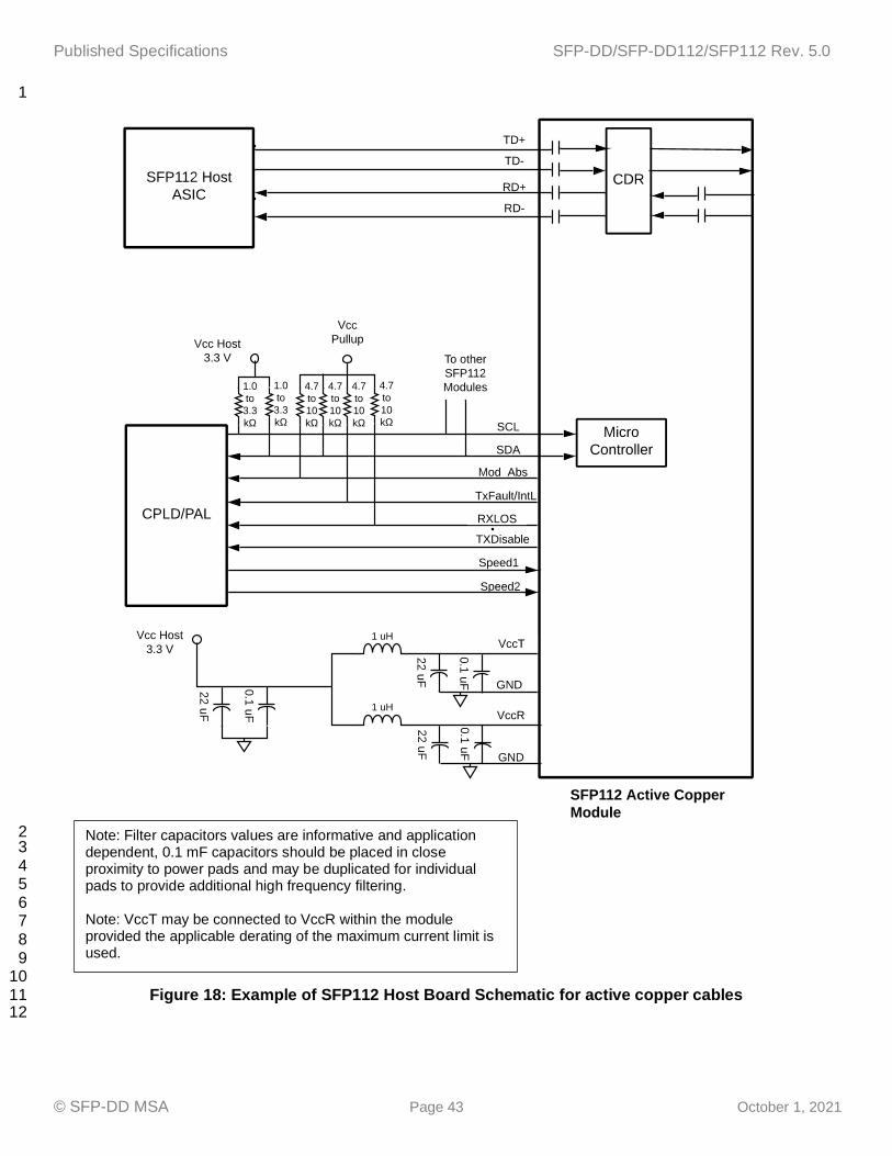
Published Specifications SFP-DD/SFP-DD112/SFP112 Rev. 5.0
© SFP-DD MSA Page 43 October 1, 2021
1
2 3 4 5 6 7 8 9 10
Figure 18: Example of SFP112 Host Board Schematic for active copper cables 11 12
Note: Filter capacitors values are informative and application dependent, 0.1 mF capacitors should be placed in close proximity to power pads and may be duplicated for individual pads to provide additional high frequency filtering. Note: VccT may be connected to VccR within the module provided the applicable derating of the maximum current limit is used.

Published Specifications SFP-DD/SFP-DD112/SFP112 Rev. 5.0
© SFP-DD MSA Page 44 October 1, 2021
1 2 3 4 5 6 7
Figure 19: Example of SFP112 Host Board Schematic for passive copper cables 8
5.5 Low Speed Electrical Specification 9
Low Electrical requirements for low speed signals TxDisable, RxLOS, Speed1, Speed2, IntL/TxFault, 10 IntL/TXFaultDD, and Mod_ABS are based on Low Voltage TTL (LVTTL) [17] operating at a module supply 11 voltage Vcc of 3.3V +/- 5% and with a host supply voltage Vcc_Host range of 2.38 to 3.46V. Vcc is used as a 12 generic term for the supply voltages of VccTx, VccRx, or VccPullup. Host biasing requirements (e.g. pullup 13 resistors) are defined in 4.3 and illustrated in 5.4. 14
Note: Filter capacitors values are informative and vary depending on applications, 0.1 uF capacitors should be placed in close proximity to power pins and may be duplicated for individual pins to provide additional high frequency filtering. Note: Recommended filtering is only valid for dedicated passive copper cable ports. For ports supporting both passive and active modules use recommended filtering from Figure 17 or Figure 18.

Published Specifications SFP-DD/SFP-DD112/SFP112 Rev. 5.0
© SFP-DD MSA Page 45 October 1, 2021
1 Electrical requirements for the TWI signals, SCL and SDA are based on Low Voltage CMOS (LVCMOS) [17] 2 operating at Vcc and compatible with [19]. Host biasing requirements (e.g. pullup resistors) are defined in 5.3 3 and illustrated in 5.4. Capacitance loading requirements are defined in Table 15 and tradeoffs are illustrated in 4 Figure 20. 5 6
5.5.1 TWI Logic Levels and Bus Loading 7
The SFP112 low speed electrical specifications are given in Table 15. Implementations compliant to this 8 specification ensures compatibility between host bus initiator and TWI. Tradeoffs among Pull up resistor 9 values, bus capacitance and rise time are shown in Figure 20. 10 11
12 Table 15- Low Speed Control and Sense Signals 13
Parameters Symbol Min Max Unit Condition
SCL and SDA VOL 0 0.4 V open-drain or open-collector at 3 mA sink current: VDD > 2 V, IOL=3.0 mA for fast mode, 20 mA for fast mode plus
SCL and SDA VIL -0.3 Vcc*0.3 V
VIH Vcc*0.7 Vcc+0.5 V
Capacitance for SCL and SDA I/O signal
Ci 14 pF
Total bus capacitive load for SCL and SDA
Cb 100 pF For 400 kHz clock rate use 3.0 k Pullup
resistor, max. For 1000 kHz clock rate refer to Figure 7.
200 pF For 400 kHz clock rate use 1.6 k pullup
resistor max. For 1000 kHz clock rate refer to Figure 7.
TxDisable, Speed1, Speed2
VIL -0.3 0.8 V For 0V<Vin<Vcc
VIH 2 Vcc+0.3 V
TxDisable, Speed1, Speed2
|Iin| 360 A
Mod_ABS
VOL 0 0.4 V IOL=2.0 mA, Mod_ABS can be implemented as a short-circuit to GND on the module
RxLOS, TxFault/IntL VOL -0.3 0.40 V 4.7 k Pullup resistor to Vcc_Host where
Vcc_Host_min<Vcc_Host<Vcc_Host_max IOH -50 37.5 uA
14

Published Specifications SFP-DD/SFP-DD112/SFP112 Rev. 5.0
© SFP-DD MSA Page 46 October 1, 2021
1 Figure 20: SDA/SCL options for pull-up resistor, bus capacitance and rise/fall times 2
3
5.6 Management Interface and Timing 4
A management memory interface (such as CMIS [5], SFP+ MIS [33]) and commonly used in other form factors 5 like QSFP-DD, SFP-DD, or SFP+ enables module functionality and flexibility beyond that supported by the 6 dedicated hardware signals. Read/Write functionality and protocols are defined in SFP-8419 [29]. 7 8 Some timing requirements are critical, especially for a multi-channel device, so the interface speed may 9 optionally be increased. Byte 00 on the Lower Page or Address 128 Page 00 is used to advertise SFP112 10 using CMIS memory map [5] vs SFP+/SFP28 using SFF-8472 memory map [33]. When a classic 11 SFP+/SFP28 module is inserted into an SFP112 port the host must use the SFP+/SFP28 memory map (i.e., 12 SFF-8472 [33]). 13 14 In some applications, muxing or demuxing may occur in the module. In this specification, all references to 15 channel numbers are based on the electrical connector interface channels, unless otherwise indicated. In 16 cases where a status or control aspect is applicable only to channels after muxing or demuxing has occurred, 17 the status or control is intended to apply to all channels in the mux group, unless otherwise indicated. 18 19 Timing requirements for the TWI signals, SCL and SDA are compatible with NXP I2C-bus specifications [19]. 20 21 22 23 24 25 26 27 28 29 30 31

Published Specifications SFP-DD/SFP-DD112/SFP112 Rev. 5.0
© SFP-DD MSA Page 47 October 1, 2021
1
5.6.1 Management Timing Specification 2
The SFP112 TWI and memory management timing illustrated in in Figure 21 and the parameters given in 3 Table 16. Implementations compliant to these specifications ensure compatibility between host bus initiator 4 and the TWI. 5 6
7 Figure 21: SFP112 Two Wire Interface Timing 8
9 10 11

Published Specifications SFP-DD/SFP-DD112/SFP112 Rev. 5.0
© SFP-DD MSA Page 48 October 1, 2021
Table 16- Management Interface timing parameters 1 Parameters Symbol Min Max Min Max Unit Conditions
Fast Mode (400 KHz)
Fast Mode Plus (1 MHz)
Clock Frequency fSCL 0 400 0 1000 KHz
Clock Pulse Width Low tLOW 1.3 0.50 µs
Clock Pulse Width High tHIGH 0.6 0.26 µs
Time bus free before new transmission can start
tBUF 20 20 µs Between STOP and START and between ACK and ReStart
START Hold Time tHD.STA 0.6 0.26 µs The delay required between SDA becoming low and SCL starting to go low in a START
START Setup Time tSU.STA 0.6 0.26 µs The delay required between SCL becoming high and SDA starting to go low in a START
Data In Hold Time tHD.DAT 0 0 µs
Data In Setup Time tSU.DAT 0.1 0.1 µs
Input Rise Time tR 300 120 ns From (VIL, MAX=0.3*Vcc) to (VIH, MIN=0.7*Vcc)
Input Fall Time tF 300 120 ns From (VIH, MIN=0.7*Vcc) to (VIL, MAX=0.3*Vcc)
STOP Setup Time tSU.STO 0.6 0.26 µs
STOP Hold Time tHD.STO 0.6 0.26 µs
Serial Interface Clock Holdoff “Clock Stretching”
T_clock_hold
500 500 s Maximum time the SFP112 module may hold the SCL line low before continuing with a read or write operation
Complete Single or Sequential Write
tWR
80 80 ms Complete (up to) 8 Byte Write
Accept a single or sequential write to volatile memory
tNACK 10 10 ms Time to complete a Single or Sequential Write to volatile registers.
Time to complete a memory bank/page
tBPC 10 10 ms Time to complete a memory bank and/or page change.
Endurance (Write Cycles)
50K 50k cycles Module Case Temperature = 70
oC
2
5.6.1.1 Bus timing tBUF 3
The timing attribute tBUF is the bus free time between sequential TWI transactions, see Figure 22. It’s 4 measured from the low to high SDA edge of the Stop condition of the Write transaction to the high to low SDA 5 edge of the Start condition for the next transaction. 6 7
5.6.1.2 Bus timing tWR 8
The timing attribute tWR is the time required for a module to complete its internally timed write cycle after a 9 single or sequential write to non-volatile memory before the next basic management operation can be 10 accepted, see Figure 22. It’s measured from the low to high SDA edge of the Stop condition of the Write 11 transaction to the high to low SDA edge of the Start condition for the next transaction. 12

Published Specifications SFP-DD/SFP-DD112/SFP112 Rev. 5.0
© SFP-DD MSA Page 49 October 1, 2021
1 Figure 22: Bus timing tWR 2
3
5.6.1.3 Bus timing tNACK 4
The timing attribute tNACK is the time required for a module to complete its internally timed write cycle after a 5 single or sequential write to volatile memory before the next basic management operation can be accepted, 6 see Figure 23. It’s measured from the low to high SDA edge of the Stop condition of the Write transaction to 7 the high to low SDA edge of the Start condition for the next transaction. 8
9 Figure 23: Bus timing tNACK 10
11

Published Specifications SFP-DD/SFP-DD112/SFP112 Rev. 5.0
© SFP-DD MSA Page 50 October 1, 2021
5.6.1.4 Bus timing tBPC 1
The timing attribute tBPC is the time required for a module to complete the change for the requested Bank 2 and/or Page selection, see Figure 24. It’s measured from the low to high SDA edge of the Stop condition of 3 the Write transaction to the high to low SDA edge of the Start condition for the next transaction. 4
5 Figure 24: Bus timing tBPC 6
7 8 9 10 11 12

Published Specifications SFP-DD/SFP-DD112/SFP112 Rev. 5.0
© SFP-DD MSA Page 51 October 1, 2021
5.7 Timing for soft control and status functions 1
Timing for SFP112 soft control and status functions are described in Table 17. Squelch and disable timings 2 are defined in Table 18. 3 4
Table 17- Timing for SFP112 soft control and status functions Parameters Symbol Min Max Unit Conditions
MgmtInitDuration
Max MgmtInit Duration
2000 ms Time from power on1 to hot plug or rising edge of reset until completion of the MgmtInit State
ResetL Assert Time t_reset_init 10
µs Minimum pulse time on the ResetL signal to initiate a module reset.
IntL Assert Time ton_IntL 200 ms Time from occurrence of condition triggering IntL until Vout:IntL=Vol
IntL Deassert Time toff_IntL 500 µs Time from clear on read2 operation of associated flag until Vout:IntL=Voh. This includes deassert times for Rx LOS, TXFault and other flag bits.
Rx LOS Assert Time ton_los 200 ms Time from Rx LOS condition present to Rx LOS bit set (value = 1b), LOS signal asserted and IntL asserted 4.
Rx LOS Assert Time (optional fast mode)
ton_losf 1 ms Time from Rx LOS state to Rx LOS bit set (value = 1b) and LOS signal asserted IntL asserted 4.
TXFault Assert Time ton_TxFault 200 ms Time from TXFault state to TXFault bit set (value=1b) and IntL asserted.
Flag Assert Time ton_flag 200 ms Time from occurrence of condition triggering flag to associated flag bit set (value=1b) and IntL asserted.
Mask Assert Time ton_mask 100 ms Time from mask bit set (value=1b)3 until associated IntL assertion is inhibited
Mask Deassert Time toff_mask 100 ms Time from mask bit cleared (value=0b)3 until associated IntL operation resumes
DataPathDeinit Max
Duration5
DataPathDeinit_MaxDuration see CMIS memory P01h: B144
DataPathInit Max
Duration5
DataPathInit_MaxDuration see CMIS memory P01h: B144
Module Pwr Up Max
Duration6
ModulePwrUp_MaxDuration see CMIS memory P01h: B167
ModulePwrDn Max
Duration6
ModulePwrDn_MaxDuration see CMIS memory P01h: B167
Data Path TX Turn On
Max Duration5
DataPathTxTurnOn_MaxDuration see CMIS memory P01h: B168
Data Path TX Turn Off
Max Duration5
DataPathTxTurnOff_MaxDuration see CMIS memory P01h: B168
Notes: 1. Power on is defined as the instant when supply voltages reach and remain at or above the minimum level specified in
Table 21. 2. Measured from low to high SDA edge of the Stop condition of the read transaction. 3. Measured from low to high SDA edge of the Stop condition of the write transaction. 4. Rx LOS condition is defined at the optical input by the relevant standard. 5. Measured from the low to high SDA edge of the Stop condition of the Write transaction until the IntL for the state
change Vout:IntL=Vol, unless the module advertises a less than 1 ms duration in which case there is no defined measurement.
6. Measured from the low to high SDA edge of the Stop condition of the Write transaction until the IntL for the state change Vout:IntL=Vol.
5 6 7

Published Specifications SFP-DD/SFP-DD112/SFP112 Rev. 5.0
© SFP-DD MSA Page 52 October 1, 2021
Table 18- I/O Timing for Squelch & Disable
Parameters Symbol Max Unit Conditions
Rx Squelch Assert Time ton_Rxsq 100 ms Time from loss of Rx input signal until the squelched output condition is reached, see 5.8.1
Rx Squelch Deassert Time
toff_Rxsq 10 s Time from resumption of Rx input signals until normal Rx output condition is reached, see 5.8.1
Tx Squelch Assert Time ton_Txsq 400 ms Time from loss of Tx input signal until the squelched output condition is reached, see 5.8.2
Tx Squelch Deassert
Time toff_Txsq 10 s Time from resumption of Tx input signals until normal
Tx output condition is reached, see 5.8.2
Tx Disable Assert Time ton_txdis 100 ms Time from the stop condition of the Tx Disable write sequence 1 until optical output falls below 10% of nominal, see note 2 and 3.
Tx Disable Assert Time (optional fast mode)
ton_txdisf 3 ms Time from Tx Disable bit set (value = 1b)1 until optical output falls below 10% of nominal, see note 2 and 3.
Tx Disable Deassert Time toff_txdis 400 ms Time from Tx Disable bit cleared (value = 0b)1 until optical output rises above 90% of nominal, see note 2 and 3.
Tx Disable Deassert Time (optional fast mode)
toff_txdisf 10 ms Time from Tx Disable bit cleared (value = 0b)1 until optical output rises above 90% of nominal.
Rx Output Disable Assert Time
ton_rxdis 100 ms Time from Rx Output Disable bit set (value = 1b)1 until Rx output falls below 10% of nominal
Rx Output Disable Deassert Time
toff_rxdis 100 ms Time from Rx Output Disable bit cleared (value = 0b)1 until Rx output rises above 90% of nominal
Squelch Disable Assert Time
ton_sqdis 100 ms This applies to Rx and Tx Squelch and is the time from bit set (value = 0b)1 until squelch functionality is disabled.
Squelch Disable Deassert Time
toff_sqdis 100 ms This applies to Rx and Tx Squelch and is the time from bit cleared (value = 0b)1 until squelch functionality is enabled
Notes: 1. Measured from LOW to HIGH SDA signal transition of the STOP condition of the write transaction. 2. CMIS 4.0 and beyond the listed values are superseded by the advertised DataPathTxTurnOff_MaxDuration and DataPathTxTurnOn_MaxDuration times in P01h.168. 3. Listed values place a limit on the DataPathTxTurnOff_MaxDuration and DataPathTxTurnOn_MaxDuration times (P01h.168) that can be advertised by such modules (for CMIS 4.0 and beyond).
1
5.8 High Speed Electrical Specifications 2
For detailed electrical specifications see the appropriate specification, e.g. IEEE Std 802.3-2018 [12]; IEEE Std 3 802.3cd [13], 802.3ck [14]; FC-PI-6 [1], FC-PI-7[2], FC-PI-8 [3]; OIF-CEI-4.0 [20], or the InfiniBand 4 specifications [16]. 5 6 Partial or complete squelch specifications may be provided in the appropriate specification. Where squelch is 7 not fully defined by the appropriate specification, the recommendations given in clause 5.8.1 and 5.8.2 may be 8 used. 9 10
5.8.1 RD0+, RD0- 11
RD(n)+/- are SFP112 module receiver data outputs. Rx(n)+/- are AC-coupled 100 differential lines that 12 should be terminated with 100 Ohms differentially at the Host ASIC(SerDes). The AC coupling is inside the 13 SFP112 module and not required on the Host board. When properly terminated, the differential voltage swing 14 shall be less than or equal to 900 mVpp or the relevant standard, whichever is less. 15 16 Output squelch for loss of optical input signal, hereafter RX Squelch, is required and shall function as follows. 17 In the event of the Rx input signal on optical lane/lanes becomes equal to or less than the level required to 18

Published Specifications SFP-DD/SFP-DD112/SFP112 Rev. 5.0
© SFP-DD MSA Page 53 October 1, 2021
assert LOS, then the electrical receiver output shall be squelched. SFP112 may have one or more Rx optical 1 lanes associated with the electrical Rx output as shown in Table 24. In the squelched state output impedance 2 levels are maintained while the differential voltage amplitude shall be less than 50 mVpp. 3 4 In normal operation the default case has RX Squelch active. Rx Squelch can be deactivated using Rx 5 Squelch Disable through the 2-wire serial interface. 6
5.8.2 TD0+, TD0- 7
TD(n)+/- are SFP112 module transmitter data inputs. They are AC-coupled 100 Ohm differential lines with 8 100 Ohm differential terminations inside the SFP112 optical module. The AC coupling is implemented inside 9 the SFP112 optical module and not required on the Host board. 10 11 Output squelch for loss of electrical signal, hereafter TX Squelch, is an optional function. Where implemented 12 it shall function as follows. In the event of the differential, peak-to-peak electrical signal amplitude on electrical 13 input channel is less than 70 mVpp, the transmitter optical output/outputs shall be squelched and the 14 associated TxLOS flag set. The loss of the incoming electrical input channels causes the optical output 15 channel/channels to be squelched. 16 17 For applications, e.g., Ethernet, where the transmitter off condition is defined in terms of average power, 18 squelching by disabling the transmitter is recommended and for applications, e.g. InfiniBand, where the 19 transmitter off condition is defined in terms of OMA, squelching the transmitter by setting the OMA to a low 20 level is recommended. 21 22 In module operation, where TX Squelch is implemented, the default case has TX Squelch active. TX Squelch 23 can be deactivated using TX Squelch Disable through the 2-wire serial interface. TX Squelch is an optional 24 function. If TX squelch is implemented, the disable squelch must be provided. 25 26
5.9 Rate Select Hardware Control 27
The module provides 2 inputs Speed1 and Speed2 that can optionally be used for rate selection as defined in 28 Table 19. Speed1 controls the receive path signaling rate and Speed2 controls the transmit path signaling rate 29 capability. 30 31 The rate select functionality can also be controlled by software as defined by the SFP112 management 32 specification. 33 34 For 64 GFC FC-PI-8 [3] operation link speed is determined with FC Link Speed Negotiation (LSN) exchange 35 while the link is operating at 32 GFC. 36 37
Table 19- Rate Select Hardware Control 38
Parameters State Conditions
Speed1 Low RX signaling rate of 14.025 GBd (16 GFC)1
High RX signaling rate of 28.05 GBd (32 GFC)
Speed2 Low TX signaling rate of 14.025 GBd (16 GFC) 1
High TX signaling rate of 28.05 GBd (32 GFC) Note 1: For SFP112 operating at 128 GFC there is no requirement for 16 GFC or rate select.
39 40 41 42 43

Published Specifications SFP-DD/SFP-DD112/SFP112 Rev. 5.0
© SFP-DD MSA Page 54 October 1, 2021
5.10 Power Requirements 1
2 SFP112 has two designated power supply pins VccT and VccR in the connector. Power is applied 3 concurrently to VccT and VccR. 4 5 A host board together with the SFP112 module(s) forms an integrated power system. The host supplies stable 6 power to the module. The module limits electrical noise coupled back into the host system and limits inrush 7 charge/current during hot plug insertion. 8 9 All power supply requirements in Table 21 shall be met at the maximum power supply current. No power 10 sequencing of the power supply is required of the host system since the module sequences the contacts in the 11 order of ground, supply and signals during insertion. 12 13
5.10.1 Power Classes and Maximum Power Consumption 14
SFP112 power classes are defined in Table 20. Since different classes of modules exist with pre-defined 15 maximum power consumption limits, it is necessary to avoid exceeding the system power supply limits and 16 cooling capacity when a module is inserted into a system designed to only accommodate lower power 17 modules. It is recommended that the host identify the power class of the module before allowing the module 18 to go into high power mode. 19 20 Power levels associated with classifications of modules are shown in Table 20. 21 22
Table 20- Power Classification 23 Power Class Max Power (W) CMIS Register
1 1.0 Direct readout of Page 00h Byte 200[000xxxxx]
2 1.5 Direct readout of Page 00h Byte 200[001xxxxx]
3 2.0 Direct readout of Page 00h Byte 200[010xxxxx]
4 3.5 Direct readout of Page 00h Byte 200[011xxxxx]
5 5.0 Direct readout of Page 00h Byte 200[100xxxxx]
6 reserved NA
7 reserved NA
81 > 5 W Direct readout of Page 00h Byte 200[111xxxxx]
Note: 1. When a module reports power class 8 the host must read CMIS Page 00h Byte 201 to determine
module power dissipation. Please see CMIS Byte 201 register definition for more information.
24 In general, the higher power classification levels are associated with higher data rates and longer reaches. 25 The system designer is responsible for ensuring that the maximum case temperature does not exceed the 26 case temperature requirements. 27 28 29

Published Specifications SFP-DD/SFP-DD112/SFP112 Rev. 5.0
© SFP-DD MSA Page 55 October 1, 2021
5.10.2 Host Board Power Supply Filtering 1
The host board should use the power supply filtering equivalent to that shown in Figure 25. 2 3
4 Figure 25: SFP112 Recommended Host Board Power Supply Filtering 5
6 7
Any voltage drop across a filter network on the host is counted against the host DC set point accuracy 8 specification. Inductors with DC Resistance of less than 0.1 Ohm should be used in order to maintain the 9
required voltage at the Host Card Edge Connector. It is recommended that the 22 F capacitors each have an 10
equivalent series resistance of 0.22 ohms. 11 12 The specifications for the power supply are shown in Table 21. The limits in Table 21 apply to the combined 13 current that flows through all inductors in the power supply filter (represents ICC host in Figure 25). An 14 example test method for measuring inrush current can is Keysight Technologies application brief 5991-15 2778EN.pdf. 16
5.10.3 Module Power Supply Specification 17
In order to avoid exceeding the host system power capacity, upon hot-plug, power cycle or reset, all SFP112 18 modules shall power up in Low Power Mode if TxDisable is asserted. If TxDisable is not asserted the module 19 will proceed to High Power Mode without host intervention. Figure 26 shows waveforms for maximum 20 instantaneous, sustained and steady state currents for Low Power and High Power modes. Specification 21 values for maximum instantaneous, sustained and steady state currents at each power class are given in 22 Table 21. 23 24
Note: Filter capacitors values are informative and vary depending on applications. VccT may be connected to VccR provided the applicable derating of the maximum current limit is used.
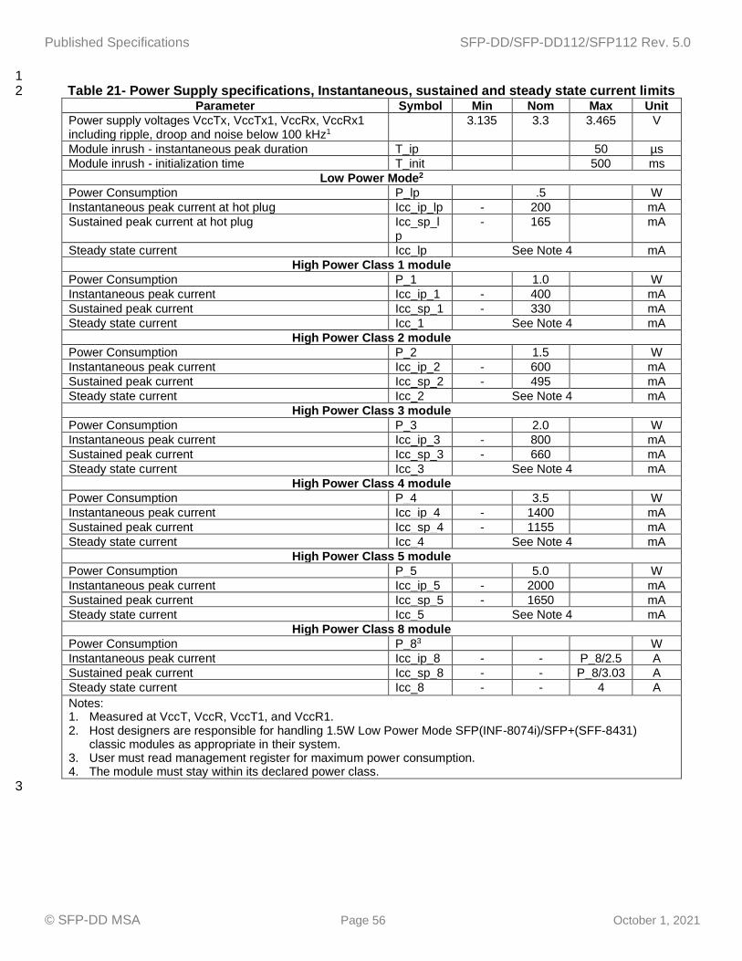
Published Specifications SFP-DD/SFP-DD112/SFP112 Rev. 5.0
© SFP-DD MSA Page 56 October 1, 2021
1 Table 21- Power Supply specifications, Instantaneous, sustained and steady state current limits 2
Parameter Symbol Min Nom Max Unit
Power supply voltages VccTx, VccTx1, VccRx, VccRx1 including ripple, droop and noise below 100 kHz1
3.135 3.3 3.465 V
Module inrush - instantaneous peak duration T_ip 50 µs
Module inrush - initialization time T_init 500 ms
Low Power Mode2
Power Consumption P_lp .5
W
Instantaneous peak current at hot plug Icc_ip_lp - 200
mA
Sustained peak current at hot plug Icc_sp_lp
- 165
mA
Steady state current Icc_lp See Note 4 mA
High Power Class 1 module
Power Consumption P_1 1.0
W
Instantaneous peak current Icc_ip_1 - 400
mA
Sustained peak current Icc_sp_1 - 330
mA
Steady state current Icc_1 See Note 4 mA
High Power Class 2 module
Power Consumption P_2
1.5
W
Instantaneous peak current Icc_ip_2 - 600
mA
Sustained peak current Icc_sp_2 - 495
mA
Steady state current Icc_2 See Note 4 mA
High Power Class 3 module
Power Consumption P_3
2.0
W
Instantaneous peak current Icc_ip_3 - 800
mA
Sustained peak current Icc_sp_3 - 660
mA
Steady state current Icc_3 See Note 4 mA
High Power Class 4 module
Power Consumption P_4
3.5
W
Instantaneous peak current Icc_ip_4 - 1400
mA
Sustained peak current Icc_sp_4 - 1155
mA
Steady state current Icc_4 See Note 4 mA
High Power Class 5 module
Power Consumption P_5
5.0
W
Instantaneous peak current Icc_ip_5 - 2000
mA
Sustained peak current Icc_sp_5 - 1650
mA
Steady state current Icc_5 See Note 4 mA
High Power Class 8 module
Power Consumption P_83
W
Instantaneous peak current Icc_ip_8 - - P_8/2.5 A
Sustained peak current Icc_sp_8 - - P_8/3.03 A
Steady state current Icc_8 - - 4 A
Notes: 1. Measured at VccT, VccR, VccT1, and VccR1. 2. Host designers are responsible for handling 1.5W Low Power Mode SFP(INF-8074i)/SFP+(SFF-8431)
classic modules as appropriate in their system. 3. User must read management register for maximum power consumption. 4. The module must stay within its declared power class.
3

Published Specifications SFP-DD/SFP-DD112/SFP112 Rev. 5.0
© SFP-DD MSA Page 57 October 1, 2021
1
Instantaneous peak, max
Sustained peak, max
Steady state, max
Icc ip lp
Icc sp lp
Icc lp
LOW POWER MODETransmitters OFF
HIGH POWER MODETransmitters ON
Icc Host (ma)
t (ms)
Hot PlugInstant
Host Enables High Power Mode
T_ip
Host Enables Transmitters
HIGH POWER MODETransmitters OFF
T_init
T_ip
T_init
T_init
T_ip
TxOff state inrush current graph is informative. It cannot exceed the High
power mode Transmitter On currents. No currents or power consumption
are specified
2 Figure 26: Instantaneous and sustained peak currents for Icc Host (see Table 21) 3
4
5.10.4 Host Board Power Supply Noise Output 5
The host shall generate an effective weighted integrated spectrum RMS noise less than the eN_Host value in 6 Table 21 when tested by the methods of SFF-8431 [30] D.17.1 with the following exceptions: 7
a. The truncated function equation with coefficients from Table 22. 8 b. The resistor shall draw the maximum rated current per contact. 9 c. The frequency response of the truncated function is illustrated in Figure 27. 10
11 Table 22- Truncated Filter Response Coefficients for Host Power Supply Noise Output 12
13
Frequency a b c d e 10 Hz < f < 240.2 Hz 0 0 0 0 -0.1
240.2 Hz < f < 24.03 kHz 0.3784 -3.6045 12.694 -19.556 11.002
24.03 kHz < f < 360.4 kHz -22.67038 430.392 -3053.779 9574.26 -11175.98
360.4 kHz < f < 12.6 MHz 3.692166 -91.467 838.80 -3400.38 5139.285
12.6 MHz < f < 24 MHz 0 0 0 0 -60
14

Published Specifications SFP-DD/SFP-DD112/SFP112 Rev. 5.0
© SFP-DD MSA Page 58 October 1, 2021
1 Figure 27: Truncated Transfer Response for Host Board Power Supply Noise Output measurement 2
3
5.10.5 Module Power Supply Noise Output 4
The SFP112 modules when plugged into a reference module compliance board shall generate noise less than 5 the value in Table 21 when tested by the methods of SFF-8431[30], D.17.2. The module must pass module 6 power supply noise output test in all operating modes. This test ensures the module will not couple excessive 7 noise from inside the module back onto the host board. 8 9 The RMS module noise voltage output is defined in the frequency band from 10 Hz to 10 MHz. Module noise 10 shall be measured with an appropriate probing technique at the input stage of the Vcc PSU filtering network, 11 see Figure 28. 12 13
5.10.6 Module Power Supply Noise Tolerance 14
The SFP112 modules shall meet all requirements and remain fully operational in the presence of a reference 15 noise waveform described in Table 23 superimposed on the DC voltage. The reference noise waveform 16 consists of triangular sweep of supply voltage Vcc PSU from 3.135 to 3.465 while a sinusoidal 1 kHz to 1 MHz 17 noise is added to Vcc PSU. This emulates the worst case noise the module must tolerate and be fully 18 operational. The reference noise shall be injected at the input stage of the Vcc PSU filtering network, see 19 Figure 28. An appropriate probing technique is required for noise characterization. 20 21
Table 23- Power Supply Output Noise and Tolerance Specifications 22
Parameter Symbol Min Nom Max Unit Host RMS noise output 40 Hz-10 MHz (eN_Host) 25 mV
Module RMS noise output 10 Hz - 10 MHz 30 mV
Module sinusoidal power supply noise tolerance 1 kHz - 1 MHz (p-p) 1
PSNRmod 66 mV
Vcc PSU triangular tolerance waveform amplitude (p-p) 2
3.135 3.465 V
Vcc PSU triangular tolerance waveform frequency (p-p)
0.001 1000 Hz
Notes: 1. Module sinusoidal power supply noise must be added to the Vcc PSU triangular waveform. 2. Assumes nominal Vcc PSU=3.3 V.
23

Published Specifications SFP-DD/SFP-DD112/SFP112 Rev. 5.0
© SFP-DD MSA Page 59 October 1, 2021
1 Figure 28: Module Noise Injection Point 2
3 4
5.11 ESD 5
Where ESD performance is not otherwise specified, e.g., in the InfiniBand specification, the SFP112 module 6 shall meet ESD requirements given in EN61000-4-2 [8], criterion B test specification when installed in a 7 properly grounded cage and chassis. The units are subjected to 15 kV air discharges during operation and 8 8 kV direct contact discharges to the case. All the SFP112 module and host pins including high speed signal 9 pins shall withstand 1000 V electrostatic discharge based on Human Body Model per ANSI/ESDA/JEDEC JS-10 001 [9]. 11 12 13

Published Specifications SFP-DD/SFP-DD112/SFP112 Rev. 5.0
© SFP-DD MSA Page 60 October 1, 2021
1
6. Optical Port Mapping and Optical Interfaces 2
3
6.1 Electrical data input/output to optical port mapping 4
Table 24 defines the mapping of electrical TX data inputs to optical ports. The mapping of the RX optical ports 5 to electrical RX outputs is symmetric. Note that there is no defined mapping of electrical input/output to optical 6 wavelengths for WDM applications. 7 8
Table 24- Electrical data input to Optical Port Mapping 9
Electrical Data Input Reference
LC, SN, MDC SN, MDC, MPO-12
1 TX fiber 2 TX fibers
TD0+/- TX-1
TX-1
TD1+/- TX-2
10
6.2 Optical Interfaces 11
Four examples of the SFP-DD/SFP-DD112 optical interface port are a male MPO receptacle (see Figure 24), 12 a dual LC (see Figure 31), a SN receptacle (see Figure 34), or a MDC receptacle (see Figure 35). The 13 recommended location and numbering of the optical ports for each of the Media Dependent Interfaces is 14 shown in Figure 29. 15
16
17 18
Figure 29: Optical Media Dependent Interface port assignments 19
TX RX1 2 12
MPO-12
Note: The transmit and receive optical lanes shall occupy the positions depicted here when looking into the MDI receptacle with the connector keyway feature on top.
TX RX
Duplex LC
1 2
SN-Dual
1 2
MDC-Dual
TX
RX
TX
RX
TX
RX
TX
RX

Published Specifications SFP-DD/SFP-DD112/SFP112 Rev. 5.0
© SFP-DD MSA Page 61 October 1, 2021
6.2.1 MPO Optical Cable connections 1
The optical plug and receptacle for the MPO-12 connector is specified in TIA-604-5 [10], IEC 61754-7 [23] and 2 shown in Figure 30. Note: Two alignment pins are present in each receptacle. 3 4 Aligned keys are used to ensure alignment between the modules and the patchcords. The optical connector is 5 orientated such that the keying feature of the MPO receptacle is on the top. 6
7 8 9
10 Figure 30: MPO-12 Single Row optical patch cord and module receptacle 11
12
6.2.2 Duplex LC Optical Cable connection 13
The Duplex LC optical patchcord and module receptacle is specified in TIA-604-10 [11], IEC 61754-20 [24] 14 and shown in Figure 31. 15
16 17
18 19
Figure 31: Duplex LC optical patchcord and module receptacle 20 21
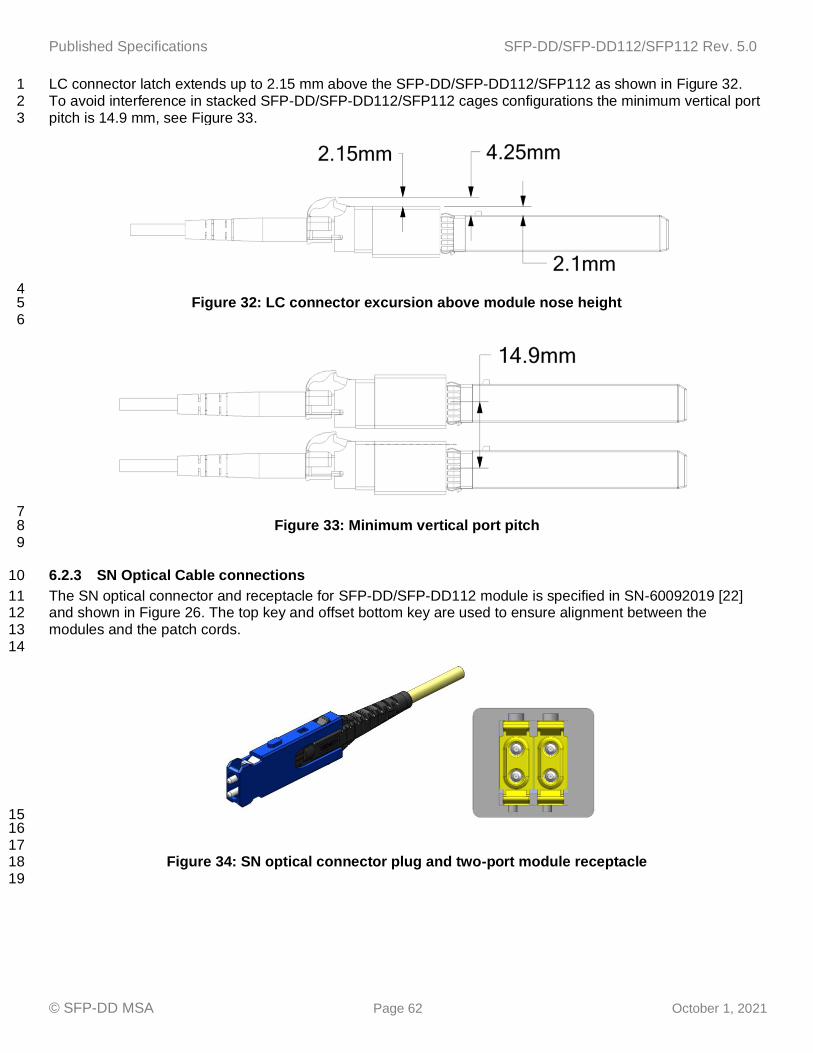
Published Specifications SFP-DD/SFP-DD112/SFP112 Rev. 5.0
© SFP-DD MSA Page 62 October 1, 2021
LC connector latch extends up to 2.15 mm above the SFP-DD/SFP-DD112/SFP112 as shown in Figure 32. 1 To avoid interference in stacked SFP-DD/SFP-DD112/SFP112 cages configurations the minimum vertical port 2 pitch is 14.9 mm, see Figure 33. 3
4 Figure 32: LC connector excursion above module nose height 5
6
7 Figure 33: Minimum vertical port pitch 8
9
6.2.3 SN Optical Cable connections 10
The SN optical connector and receptacle for SFP-DD/SFP-DD112 module is specified in SN-60092019 [22] 11 and shown in Figure 26. The top key and offset bottom key are used to ensure alignment between the 12 modules and the patch cords. 13 14
15 16 17
Figure 34: SN optical connector plug and two-port module receptacle 18 19

Published Specifications SFP-DD/SFP-DD112/SFP112 Rev. 5.0
© SFP-DD MSA Page 63 October 1, 2021
6.2.4 MDC Optical Cable connections 1
The MDC optical plug and receptacle for an SFP-DD/SFP-DD112 module is specified in USC-11383001 [25] 2 and shown in Figure 27. The optical connector is orientated such that the keying feature of the MDC 3 receptacle is on the top. 4
5 6 7
8 Figure 35: MDC optical connector plug and two-port module receptacle 9
10
6.3 Module Color Coding and Labeling 11
If provided, color coding shall be on an exposed feature of the SFP-DD/SFP-DD112 module (a feature or 12 surface extending outside of the bezel). Color code are outside the scope of this specification. 13 14 Each SFP-DD/SFP-DD112 module shall be clearly labeled. The complete labeling need not be visible when 15 the SFP-DD/SFP-DD112 module is installed, and the bottom of the device is the recommended location for the 16 label. Labeling shall include: 17 18
• Appropriate manufacturing and part number identification 19 • Appropriate regulatory compliance labeling 20 • A manufacturing traceability code. 21
22 The label should also include clear specification of the external port characteristics such as: 23 24
• Optical wavelength 25 • Required fiber characteristics 26 • Operating data rate 27 • Interface standards supported 28 • Link length supported. 29
30 The labeling shall not interfere with the mechanical, thermal or EMI features. 31 32
33

Published Specifications SFP-DD/SFP-DD112/SFP112 Rev. 5.0
© SFP-DD MSA Page 64 October 1, 2021
7. SFP-DD Mechanical and Board Definition 1
7.1 Introduction to SFP-DD and SFP-DD112 2
The cages and modules specifications defined in this chapter are illustrated in Figure 36 (press fit cage) and 3 Figure 37 (pluggable module). All Pluggable modules and direct attach cable plugs must mate to the 4 connectors and cages defined in this specification. (See SFF-8432 [31]) Heat sink/clip thermal designs are 5 application specific and not specifically defined by this specification. The SFP-DD and SFP-DD112 modules 6 and cage support both a pull tab and a bail latch solution. Details on bail latch retention and extraction 7 specifications can be found in SFF-8432. 8 9
10
11 12 13
Figure 36: Press fit cage 14

Published Specifications SFP-DD/SFP-DD112/SFP112 Rev. 5.0
© SFP-DD MSA Page 65 October 1, 2021
1 2
3 4
Type 1 module 5
6 Type 2 module 7
8 9
Figure 37: SFP-DD and SFP-DD112 Modules 10 11 12

Published Specifications SFP-DD/SFP-DD112/SFP112 Rev. 5.0
© SFP-DD MSA Page 66 October 1, 2021
7.2 SFP-DD/SFP-DD112/SFP112 Datums, Dimensions and Component Alignment 1
2 A listing of the SFP-DD/SFP-DD112/SFP112 datums for the various components are contained in Table 25. 3 To reduce the complexity of the drawings, all dimensions are considered centered unless otherwise specified. 4 Dimensions and tolerancing conform to ASME Y14.5-2009 [4]. All dimensions are in millimeters. 5 6
7 8
Table 25- Datum Description 9
Datum Description A Width Of module
B Bottom surface of module
C Leading edge of signal contact pads on module paddle card
D Hard stop on module
E Host board thru hole to accept primary cage press fit pin
F Hard stop on cage
G Bottom surface of bezel cutout
K Host board thru hole #1 to accept connector guidepost
L Host board thru hole #2 to accept connector guidepost
P Vertical center line of internal surface of cage
S Seating plane of cage on host board
Z Top surface of host board
AA Center line of module paddle card width
BB Top surface of module paddle card
CC Center line of connector slot width
DD Seating plane of connector on host board
10 11 12
13 14

Published Specifications SFP-DD/SFP-DD112/SFP112 Rev. 5.0
© SFP-DD MSA Page 67 October 1, 2021
7.3 SFP-DD Cage, Connector, Module Alignment 1
The alignment of the cage, connector and module are shown in Figure 38. 2 3
4 5
Figure 38: Cage, Connector alignment 6

Published Specifications SFP-DD/SFP-DD112/SFP112 Rev. 5.0
© SFP-DD MSA Page 68 October 1, 2021
7.4 SFP-DD/SFP-DD112 Module Mechanical Dimensions 1
The mechanical outline for the SFP-DD/SFP-DD112 modules and direct attach cables are shown in Figure 39. 2 The module shall provide a means to self-lock with the cage upon insertion. The module package dimensions 3 are defined in Figure 40. The dimensions that control the size of the module that extends outside of the cage 4 are listed as maximum dimensions per Note 4 in Figure 40. 5
6 7 8 9
10 11
Type 1 module 12
13 Type 2 module 14
15 Figure 39: Type 1 and Type 2 Modules 16
17 18 19 20

Published Specifications SFP-DD/SFP-DD112/SFP112 Rev. 5.0
© SFP-DD MSA Page 69 October 1, 2021
1 2
3
9

Published Specifications SFP-DD/SFP-DD112/SFP112 Rev. 5.0
© SFP-DD MSA Page 70 October 1, 2021
1 2 3

Published Specifications SFP-DD/SFP-DD112/SFP112 Rev. 5.0
© SFP-DD MSA Page 71 October 1, 2021
1 2
3 4
Figure 40: Detailed dimensions of module 5 6 7

Published Specifications SFP-DD/SFP-DD112/SFP112 Rev. 5.0
© SFP-DD MSA Page 72 October 1, 2021
7.5 SFP-DD/SFP-DD112/SFP112 Module Flatness and Roughness 1
2 Module flatness and roughness are specified to improve module thermal characteristics when used with a 3 riding heat sink. Relaxed specifications are used for lower power modules to reduce cost. The module flatness 4 and roughness specifications apply to the specified heat sink contact area as specified in Figure 40. 5 Specifications for Module flatness and surface roughness are shown in Table 26. 6 7
Table 26- Module flatness specifications 8 Power Class Module Flatness (mm) Surface Roughness (Ra,µm)
1 0.075 1.6
2 0.075 1.6
3 0.075 1.6
4 0.075 1.6
5 0.050 0.8
6 reserved reserved
7 reserved reserved
8 0.050 0.8
9
7.6 SFP-DD Module paddle card dimensions 10
11
12 13
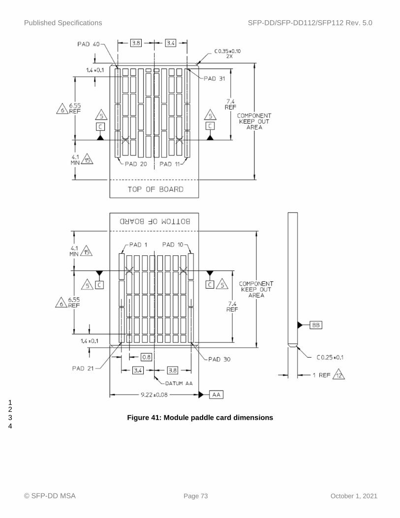
Published Specifications SFP-DD/SFP-DD112/SFP112 Rev. 5.0
© SFP-DD MSA Page 73 October 1, 2021
1 2
Figure 41: Module paddle card dimensions 3
4

Published Specifications SFP-DD/SFP-DD112/SFP112 Rev. 5.0
© SFP-DD MSA Page 74 October 1, 2021
1 2
3 Figure 42: Module pad dimensions 4
5

Published Specifications SFP-DD/SFP-DD112/SFP112 Rev. 5.0
© SFP-DD MSA Page 75 October 1, 2021
7.7 SFP-DD/SFP-DD112/SFP112 Module Extraction and Retention Forces 1
The requirements for insertion forces, extraction forces and retention forces are specified Appendix A. The 2 SFP-DD/SFP-DD112/SFP112 cage and modules are designed to ensure that excessive force applied to a 3 cable does not damage the SFP-DD cage or host connector. If any part is damaged by excessive force, it 4 should be the cable or media module and not the cage or host connector which is part of the host system. 5 Examples of module retention mechanisms are found in SFF-8432 [31] Figures 4-4 through 4-7. The contact 6 pad plating shall meet the requirements are given in 7.6. 7 8
7.8 Press fit Cage Mechanical 9
The SFP-DD Cage is shown in Figure 43 with detailed drawings in Figure 44. Recommendations for the cage 10 bezel opening are shown in Figure 46. 11 12
13 Figure 43: Press Fit 1x1 Cage 14
15

Published Specifications SFP-DD/SFP-DD112/SFP112 Rev. 5.0
© SFP-DD MSA Page 76 October 1, 2021
1 2 3 4 5
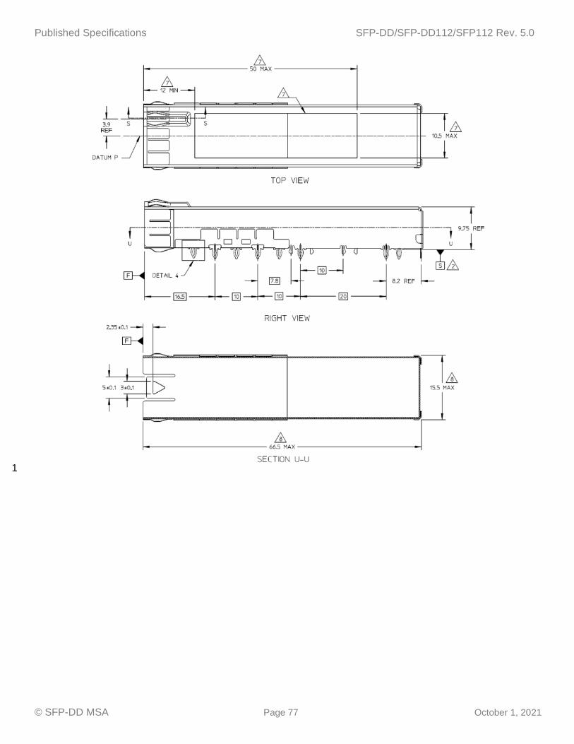
Published Specifications SFP-DD/SFP-DD112/SFP112 Rev. 5.0
© SFP-DD MSA Page 77 October 1, 2021
1

Published Specifications SFP-DD/SFP-DD112/SFP112 Rev. 5.0
© SFP-DD MSA Page 78 October 1, 2021
1 2
3 Figure 44: Press Fit 1x1 Cage Design 4
5
6

Published Specifications SFP-DD/SFP-DD112/SFP112 Rev. 5.0
© SFP-DD MSA Page 79 October 1, 2021
1 2
Figure 45: Press Fit Cage Detail 3

Published Specifications SFP-DD/SFP-DD112/SFP112 Rev. 5.0
© SFP-DD MSA Page 80 October 1, 2021
1 2
Figure 46: 1 x n bezel opening 3 4 5

Published Specifications SFP-DD/SFP-DD112/SFP112 Rev. 5.0
© SFP-DD MSA Page 81 October 1, 2021
7.9 SMT Electrical Connector Mechanical 1
The SFP-DD Connector is a 40-contact, right angle connector. The SMT connector is shown in Figure 47 with 2 detailed drawings in Figure 48. 3
4
5 Figure 47: SMT connector 6
7

Published Specifications SFP-DD/SFP-DD112/SFP112 Rev. 5.0
© SFP-DD MSA Page 82 October 1, 2021
1 2
3

Published Specifications SFP-DD/SFP-DD112/SFP112 Rev. 5.0
© SFP-DD MSA Page 83 October 1, 2021
1 2 3 4
5 6 7 8
9 Figure 48: 1x1 Connector Design and Host PCB Pin Numbers 10
11 12

Published Specifications SFP-DD/SFP-DD112/SFP112 Rev. 5.0
© SFP-DD MSA Page 84 October 1, 2021
7.9.1 SMT connector and cage host PCB layout 1
A typical host board mechanical layout for attaching the SFP-DD SMT Connector and press fit Cage System is 2 shown in Figure 49. Location of the pattern on the host board is application specific. 3 4 To achieve 25-50 Gbps performance pad dimensions and associated tolerances must be adhered, and 5 attention paid to the host board layout. 6 7 8 9
10

Published Specifications SFP-DD/SFP-DD112/SFP112 Rev. 5.0
© SFP-DD MSA Page 85 October 1, 2021
1
2 3
Figure 49: Host PCB Mechanical Layout 4 5

Published Specifications SFP-DD/SFP-DD112/SFP112 Rev. 5.0
© SFP-DD MSA Page 86 October 1, 2021
8. SFP-DD112 Mechanical and Board Definition 1
SFP-DD112 module mechanical specifications are compatible with SFP-DD module mechanical specifications 2 in chapter 7, below are the list of relevant SFP-DD sections applicable to SFP-DD112: 3
- 7.1 Introduction to SFP-DD and SFP-DD112 4 - 7.2 SFP-DD/SFP-DD112/SFP112 Datums, Dimensions and Component Alignment 5 - 7.4 SFP-DD/SFP-DD112 Module Mechanical Dimensions 6 - 7.5 SFP-DD/SFP-DD112/SFP112 Module Flatness and Roughness 7 - 7.7 SFP-DD/SFP-DD112/SFP112 Module Extraction and Retention Forces. 8 - 9
8.1 Introduction 10
The module paddle card dimensions of the SFP-DD112 have been improved to support 100 Gb/s PAM4 (up to 11 56 GBd) serial data rates, see Section 4. 12 13 SFP-DD112 supports multiple connector/cage form factors. SFP-DD112 cages/connectors/modules are 14 compatible with SFP-DD cages/connectors/modules, SFP-DD112 cages/connectors also accepts 15 SFP+/SFP28 [30]/[28] family of modules. Examples of SFP-DD112 cages are: 16
• 1x1 surface mount connector/cage. 17 18
8.2 SFP-DD112 module mechanical dimensions 19
The mechanical outline for the SFP-DD112 module and direct attach cables are identical to Figure 22. The 20 module shall provide a means to self-lock within the cage upon insertion. The module package dimensions are 21 identical to Figure 23 with exception of bottom view shown in Figure 50. For SFP-DD112 modules the bottom 22 surface of the module within the cage shall be flat without a pocket. The options for the position of the label 23 could include the bottom surface of the module that protrudes outside the bezel of the cage or etched into the 24 metal surface. 25 26 Caution should be exercised that any etchings do not affect thermal performance. Flatness and roughness 27 specs are defined in 7.5 apply to both top and bottom surfaces of SFP-DD112 module. 28 29
30 Figure 50: SFP-DD112 Module Bottom View Details 31
32

Published Specifications SFP-DD/SFP-DD112/SFP112 Rev. 5.0
© SFP-DD MSA Page 87 October 1, 2021
8.3 SFP-DD112 Improved Module paddle card dimensions 1
2
3 4

Published Specifications SFP-DD/SFP-DD112/SFP112 Rev. 5.0
© SFP-DD MSA Page 88 October 1, 2021
1
2 Figure 51: Improved module paddle card dimensions 3
4
5
6

Published Specifications SFP-DD/SFP-DD112/SFP112 Rev. 5.0
© SFP-DD MSA Page 89 October 1, 2021
1 Figure 52: Improved module pad dimensions 2
3

Published Specifications SFP-DD/SFP-DD112/SFP112 Rev. 5.0
© SFP-DD MSA Page 90 October 1, 2021
1
8.4 Press fit Cage Mechanical 2
3 SFP-DD112 press fit cage is shown in Figure 53 with detailed drawings in Figure 44. SFP-DD112 cage bezel 4 opening is identical to SFP-DD cage bezel as shown in Figure 46. 5 6
7 8 9
Figure 53: Press Fit 1x1 Cage 10 11 12
13 14 15 16 17 18 19
20
21
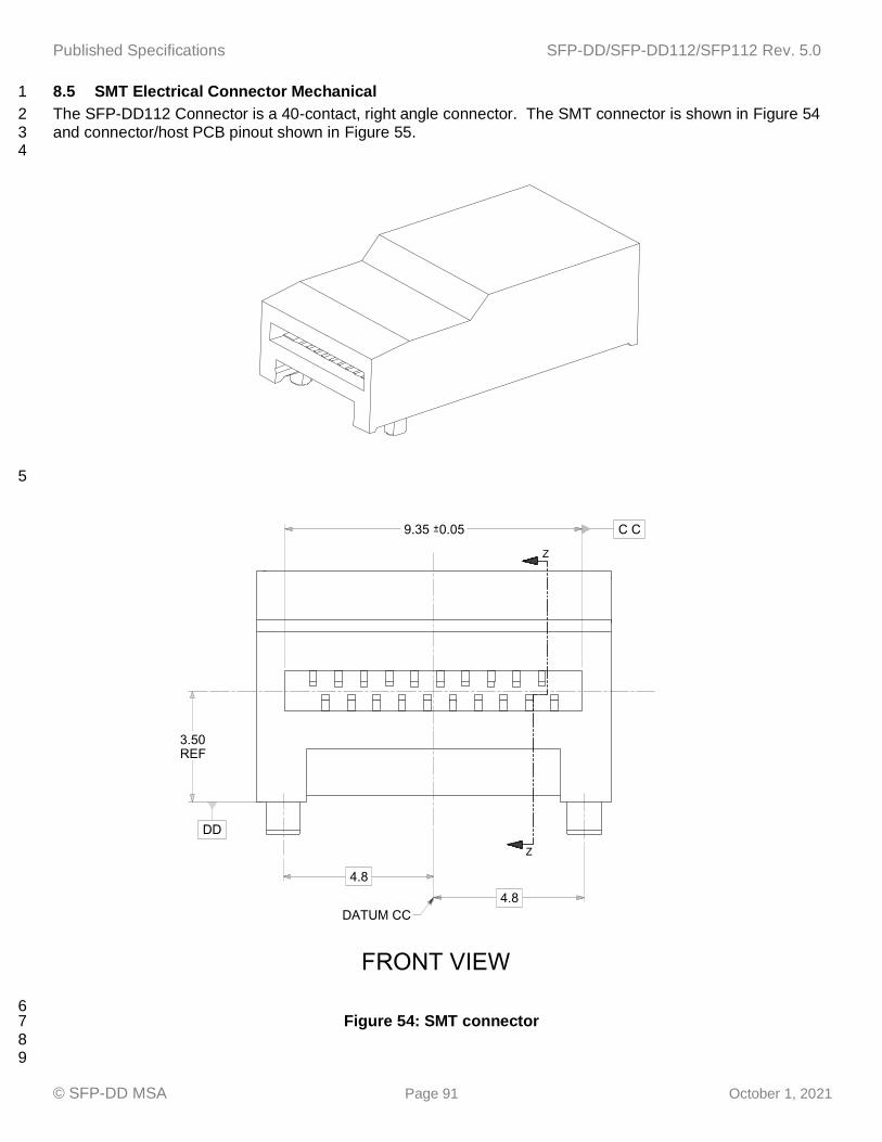
Published Specifications SFP-DD/SFP-DD112/SFP112 Rev. 5.0
© SFP-DD MSA Page 91 October 1, 2021
8.5 SMT Electrical Connector Mechanical 1
The SFP-DD112 Connector is a 40-contact, right angle connector. The SMT connector is shown in Figure 54 2 and connector/host PCB pinout shown in Figure 55. 3 4
5
6 Figure 54: SMT connector 7
8 9

Published Specifications SFP-DD/SFP-DD112/SFP112 Rev. 5.0
© SFP-DD MSA Page 92 October 1, 2021
1
2 3
4
5 6
7 Figure 55: 1x1 Connector Design and Host PCB Pin Numbers 8
9 10 11 12
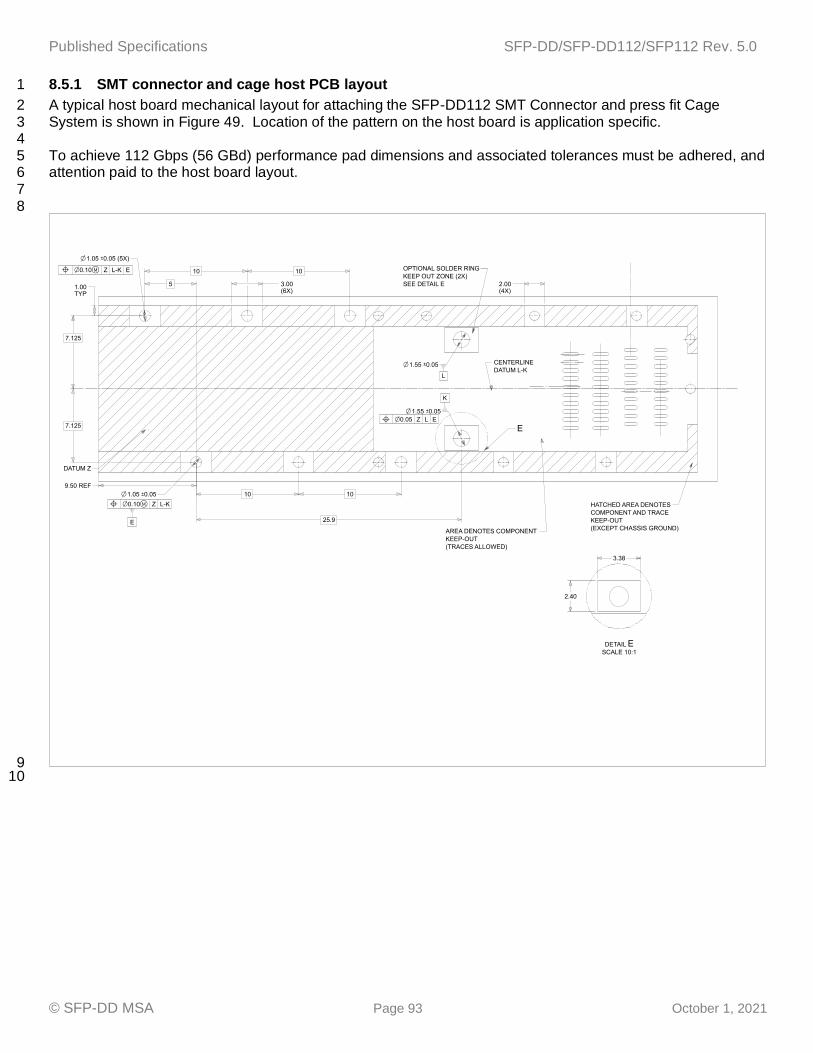
Published Specifications SFP-DD/SFP-DD112/SFP112 Rev. 5.0
© SFP-DD MSA Page 93 October 1, 2021
8.5.1 SMT connector and cage host PCB layout 1
A typical host board mechanical layout for attaching the SFP-DD112 SMT Connector and press fit Cage 2 System is shown in Figure 49. Location of the pattern on the host board is application specific. 3 4 To achieve 112 Gbps (56 GBd) performance pad dimensions and associated tolerances must be adhered, and 5 attention paid to the host board layout. 6 7 8
9 10

Published Specifications SFP-DD/SFP-DD112/SFP112 Rev. 5.0
© SFP-DD MSA Page 94 October 1, 2021
1 2
3 4
5 6
Figure 56: Host PCB Mechanical Layout 7

Published Specifications SFP-DD/SFP-DD112/SFP112 Rev. 5.0
© SFP-DD MSA Page 95 October 1, 2021
9. SFP112 Mechanical and Board Definition 1
SFP112 module mechanical specifications are compatible with SFP+/SFP28 [30]/[28]module mechanical 2 specifications. Below are the list of relevant SFP+/SFP28 and SFP-DD sections applicable to SFP112: 3
- IPF General descriptions, [31][31] Chapter 3.0 4 - IPF Modules Dimensions, Retention/Extraction, and Durability, [31] Chapter 4 5 - IPF Cage Requirements, [31], Chapter 5 6 - SFP Single Cage Host Board Mechanical Layout, [26] Chapter 4A 7 - SFP+ Canged Cage Host Board Mechanical Layout, [32] Chapter 4 8 - SFP-DD/SFP-DD112/SFP112 Datums, Dimensions and Component Alignment, 7.2 9 - SFP-DD/SFP-DD112/SFP112 Module Flatness and Roughness, 7.5 10 - SFP-DD/SFP-DD112/SFP112 Module Extraction and Retention Forces, 7.7. 11 12
9.1 Introduction 13
The module paddle card dimensions of the SFP112 have been improved to support 100 Gb/s PAM4 (up to 56 14 GBd) serial data rates compared to SFP+/SFP [30]/[28]. 15 16 SFP112 supports multiple connector/cage form factors. All combinations of cages/connectors defined in the 17 specification are backwards compatible to accept classic SFP28 and SFP+ modules. In addition, SFP112 18 modules are compatible with SFP28/SFP+ hosts for operation at lower speed. 19 20
9.2 SFP112 Datum for Module, Cage, Connector and Host 21
A listing of the SFP112 datums for the various components are contained in Table 27. To reduce the 22 complexity of the drawings, all dimensions are considered centered unless otherwise specified. Dimensions 23 and tolerancing conform to ASME Y14.5-2009 [4]. All dimensions are in millimeters. 24 25
Table 27: SFP112 Datum 26
Datum Description
A Center line of connector slot
B Bottom surface of connector
C Round guide-post of connector
D Leading edge of signal contact pads on module paddle card
E Leading edge of low speed contact pads on module paddle card
F Front edge of module paddle card
G Top surface of module paddle card
H Center line of module paddle card width
K Host board thru hole #1 to accept connector guide-post
L Host board thru hole #2 to accept connector guide-post
M Vertical center line of Datum L and Datum K
N Top surface of host board
P Hard stop on module
R Hard stop on cage
S Host board thru hole to accept primary cage press fit pin
T Center line of module width
U Bottom surface of module
27 28

Published Specifications SFP-DD/SFP-DD112/SFP112 Rev. 5.0
© SFP-DD MSA Page 96 October 1, 2021
1
9.3 SFP112 Cage, Connector, Module Alignment 2
The alignment of the cage, connector and module are shown in Figure 57. 3
4 Figure 57: SFP112 1x1 Cage and Host PCB Layout 5

Published Specifications SFP-DD/SFP-DD112/SFP112 Rev. 5.0
© SFP-DD MSA Page 97 October 1, 2021
9.4 SFP112 module mechanical dimensions 1
SFP112 modules mechanical dimension are identical to SFP+/SFP28 [30]/[28] modules with exception of 2 viewing windows to inspect high speed pad as shown Figure 58. A SFP28/56 [28] cage can be used with the 3 SFP112 connector. For SFP112 modules the bottom surface of the module within the cage shall be flat 4 without a pocket. The options for the position and the bottom view of the label could include the bottom 5 surface of the module that protrudes outside the bezel of the cage or etched into the metal surface. Caution 6 should be exercised that any etchings do not affect thermal performance. 7 8 Flatness and roughness specs are defined in 7.5 to both top and bottom surfaces of SFP112 module. 9
NOTES APPLY TO MODULE DRAWINGS: 10
11

Published Specifications SFP-DD/SFP-DD112/SFP112 Rev. 5.0
© SFP-DD MSA Page 98 October 1, 2021
1
2
Figure 58: SFP112 High Speed Pads Viewing Windows 3

Published Specifications SFP-DD/SFP-DD112/SFP112 Rev. 5.0
© SFP-DD MSA Page 99 October 1, 2021
9.5 SFP112 Improved Module paddle card dimensions 1
The SFP112 module paddle card pad dimensions have been modified to support 112 Gb/s (56 GBd) serial 2 data rates. SFP112 module paddle card pad dimensions optimized for 56 GBd operation shown in Figure 59. 3 All other module dimensions, except for the pads are the same as the SFP+/SFP28 [30]/[28] specifications. 4
5 Figure 59: SFP112 improved module paddle card dimensions 6
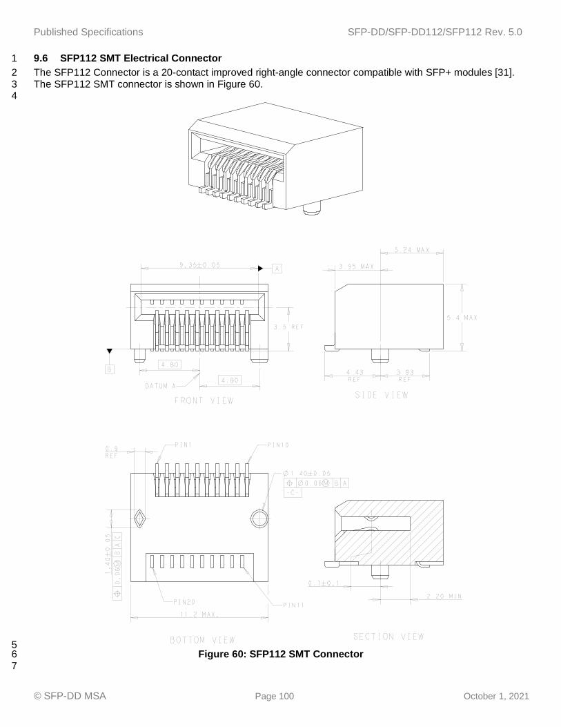
Published Specifications SFP-DD/SFP-DD112/SFP112 Rev. 5.0
© SFP-DD MSA Page 100 October 1, 2021
9.6 SFP112 SMT Electrical Connector 1
The SFP112 Connector is a 20-contact improved right-angle connector compatible with SFP+ modules [31]. 2 The SFP112 SMT connector is shown in Figure 60. 3
4
5 Figure 60: SFP112 SMT Connector 6
7

Published Specifications SFP-DD/SFP-DD112/SFP112 Rev. 5.0
© SFP-DD MSA Page 101 October 1, 2021
9.6.1 SFP112 SMT host PCB layout 1
A typical host board mechanical layout for attaching the SFP112 surface mount Connector is shown in Figure 2 61. The detailed optimized SFP112 host pad layout is shown in Figure 61 and the host PCB pad numbers 3 shown in Figure 63. Note: the cage footprint for SFP112 is the same the same as SFP cage footprint, [26] see 4 Figure 4A. 5 6 To achieve 112 Gbps (56 GBd) operation the SFP112 pad dimensions and associated tolerances have 7 improved compared to SFP+/SFP28 [30]/[28] as shown in Figure 62. One must adhere and pay attention to 8 the host board layout for 56 GBd operation. 9 10
11 Figure 61: SFP112 Host Pad Layout 12
13 14

Published Specifications SFP-DD/SFP-DD112/SFP112 Rev. 5.0
© SFP-DD MSA Page 102 October 1, 2021
1 2
Figure 62: SFP112 Detailed Host Pad Layout 3
4 Figure 63: 1x1 Connector Design and Host PCB Pad Numbers 5
6

Published Specifications SFP-DD/SFP-DD112/SFP112 Rev. 5.0
© SFP-DD MSA Page 103 October 1, 2021
10. Environmental and Thermal 1
10.1 Thermal Requirements 2
The SFP-DD/SFP-DD112/SFP112 module shall operate within one or more of the case temperatures ranges 3 defined in Table 28. The temperature ranges are applicable between 60 m below sea level and 1800 m above 4 sea level, NEBS GR-63 [18], utilizing the host systems designed airflow. 5 6
Table 28- Temperature Range Class of operation 7
Class Case Temperature Range
Standard 0°C through 70°C
Extended -5°C through 85°C
Industrial -40°C through 85°C
8 SFP-DD/SFP-DD112/SFP112 are designed to allow for up to 48 modules; stacked, ganged and/or belly-to-9 belly in a 1U 19" rack, with the appropriate thermal design for cooling/airflow. 10 11 12 13

Published Specifications SFP-DD/SFP-DD112/SFP112 Rev. 5.0
© SFP-DD MSA Page 104 October 1, 2021
Appendix A Normative Module and Connector Performance Requirements 1
A.1 Performance Tables 2
EIA-364-1000 [7] shall be used to define the test sequences and procedures for evaluating the connector 3 system described in this document. Where multiple test options are available, the manufacturer shall select 4 the appropriate option where not previously specified. The selected procedure should be noted when 5 reporting data. If there are conflicting requirements or test procedures between EIA-364 procedures and those 6 contained within this document, this document shall be considered the prevailing authority. Unless otherwise 7 specified, procedures for sample size, data, and collection to be followed as specified in EIA-364-1000. See 8 EIA-364-1000 Annex B for objectives of tests and test groups. 9 10 This document represents the minimum requirements for the defined product. Additional test conditions and 11 evaluations may be conducted within the defined EIA-364-1000 sequences. More extreme test conditions and 12 failure criteria may be imposed and still meet the requirements of this document. 13 14 Table 29 summarizes the performance criteria that are to be satisfied by the connector described in this 15 document. Most performance criteria are validated by EIA-364-1000 testing, but this test suite leaves some 16 test details to be determined. To ensure that testing is repeatable, these details are identified in Table 30. 17 Finally, testing procedures used to validate any performance criteria not included in EIA-364-1000 are 18 provided in Table 31. 19 20
Table 29- Form Factor Performance Requirements 21
Performance Parameters
Description/ Details Requirements
Mechanical/ Physical Tests Plating Type Plating type on connector contacts Precious (refer to 7.6 for plating details) Surface Treatment Surface treatment on connector contacts; if surface
treatment is applied, Test Group 6 is required Manufacturer to specify
Wipe length Designed distance a contact traverses over a mating contact surface during mating and resting at a final position. If less than 0.127 mm, test group 6 is required
Manufacturer to specify
Rated Durability Cycles
The expected number of durability cycles a component is expected to encounter over the course of its life
Connector/ cage: 100 cycles Module: 50 cycles
Mating Force1 Amount of force needed to mate a module with a connector when latches are deactivated
SFP112 module: 40 N MAX SFP-DD/SFP-DD112 module: 40 N MAX
Unmating Force1 Amount of forced needed to separate a module from a connector when latches are deactivated
SFP112 module: 12.5 N MAX SFP-DD/SFP-DD112 module: 30 N MAX
Latch Retention1 Amount of force the latching mechanism can withstand without unmating
SFP112 module: 90 N MIN SFP-DD/ SFP-DD112 module: 90 N MIN
Cage Latch Strength1
The amount of force that the cage latches can hold without being damaged.
100 N MIN
Cage Retention to Host Board1
Amount of force a cage can withstand without separating from the host board
SFP112 module: 100 N MIN SFP-DD/ SFP-DD112 module: 100 N MIN
Environmental Requirements Field Life The expected service life for a component 10 years Field Temperature The expected service temperature for a component 65°C
Electrical Requirements
Current Maximum current to which a contact is exposed in use
0.5 A per signal contact MAX 1.5 A per power contact MAX
Operating Rating Voltage
Maximum voltage to which a contact is exposed in use
30 V DC per contact MAX
Note: 1. These performance criteria are not validated by EIA-364-1000 testing, see Table 31 for test procedures and
pass/fail criteria.

Published Specifications SFP-DD/SFP-DD112/SFP112 Rev. 5.0
© SFP-DD MSA Page 105 October 1, 2021
1 2 Table 30 describes the details necessary to perform the tests described in the EIA-364-1000 test sequences. 3 Testing shall be done in accordance with EIA-364-1000 and the test procedures it identifies in such a way that 4 the parameters/ requirements defined in Table 29 are met. Any information in this table supersedes EIA-364-5 1000. 6
Table 30- EIA-364-1000 Test Details 7
Performance Parameters
Description/ Details Requirements
Mechanical/ Physical Tests Durability (preconditioning)
EIA-364-09 To be tested with connector, cage, and module. Latches may be locked out to aid in automated cycling.
No evidence of physical damage
Durability1
EIA-364-09 To be tested with connector, cage, and module. Latches may be locked out to aid in automated cycling.
No visual damage to mating interface or latching mechanism
Environmental Tests Cyclic Temperature and Humidity
EIA-364-31 Method IV omitting step 7a Test Duration B
No intermediate test criteria
Vibration EIA-364-28 Test Condition V Test Condition Letter D Test set-up: Connectors may be restrained by a plate that replicates the system panel opening as defined in this specification. External cables may be constrained to a non-vibrating fixture a minimum of 8 inches from the module. For cabled connector solutions: Wires may be attached to PCB or fixed to a non-vibrating fixture.
No evidence of physical damage -AND- No discontinuities longer than 1 μs allowed
Mixed Flowing Gas EIA-364-65 Class II See Table 4.1 in EIA-364-1000 for exposure times Test option Per EIA-364-1000 option 3
No intermediate test criteria
Electrical Tests Low Level Contact Resistance2
EIA-364-23 20 mV DC Max, 100 mA Max To include wire termination or connector-to-board termination
20 mΩ Max change from baseline
Dielectric Withstanding Voltage
EIA-364-20 Method B 300 VDC minimum for 1 minute Applied voltage may be product / application specific
No defect or breakdown between adjacent contacts -AND- 1 mA Max Leakage Current
Notes: 1. If the durability requirement on the connector is greater than that of the module, modules may be replaced after their specified durability rating. 2. The first low level contact resistance reading in each test sequence is used to determine a baseline measurement. Subsequent measurements in each sequence are measured against this baseline.
8 9 10 11 12 13 14 15 16 17 18

Published Specifications SFP-DD/SFP-DD112/SFP112 Rev. 5.0
© SFP-DD MSA Page 106 October 1, 2021
1 Table 31 describes the testing procedures necessary to validate performance criteria not validated by EIA-2 364-1000 testing. The tests are to be performed in such a way that the parameters/ requirements defined in 3 Table 29 are met. 4 5
Table 31- Additional Test Procedures 6
Tests
Test Descriptions and Details Pass/ Fail Criteria’s
Mechanical/ Physical Tests Mating Force1 EIA-364-13
Mating/ unmating rate 12.7 mm/min To be tested with cage, connector, and module. Latching mechanism deactivated (locked out).
Refer to Table 29 -AND- No physical damage to any components
Unmating Force1
Latch Retention1 EIA-364-13 Mating/ unmating rate 12.7 mm/min To be tested with cage, connector, and module. Latching mechanism engaged (not locked out).
Latch Strength An axial load applied using a static load or ramped loading to the specified load. To be tested with cage, connector, and module or module representative tool without heat sinks Latching mechanism engaged (not locked out).
Cage Retention to Host Board
Tested with module, module analog, or fixtures mated to cage. Pull cage in a direction perpendicular to the board at a rate of 25.4 mm/min to the specified force.
No physical damage to any components -AND- Cage shall not separate from board
Electrical Tests Current EIA-364-70
Method 3, 30-degree temperature rise Contacts energized: All signal and power contacts energized simultaneously
Refer to Table 29 for current magnitude
Note: 1. Values listed in Table 29 apply with or without the presence of a riding heat sink.
7 8

Published Specifications SFP-DD/SFP-DD112/SFP112 Rev. 5.0
© SFP-DD MSA Page 107 October 1, 2021
1 2
End of
Document