Session 6 Semiconductor devices...
17
Session 6 Semiconductor devices fundamentals Electronic Components and Circuits Isabel Pérez www.uc3m.es/portal/page/portal/dpto_tecnologia_electronica/Personal/IsabelPerez
Transcript of Session 6 Semiconductor devices...

Session 6
Semiconductor devicesfundamentals
Electronic Components and Circuits
Isabel Pérez
www.uc3m.es/portal/page/portal/dpto_tecnologia_electronica/Personal/IsabelPerez

Semiconductor Materials and
DiodesSKILLS
• To know the semiconductors fundamentals– Intrinsic semiconductors. Electron and hole.
– Extrinsic semiconductors. Impurity atoms (donors and aceptors).
– n-type and p-type semiconductors
• To understand the p-n junction fundamentals– p-n junction equilibrium . The space charge region.– p-n junction equilibrium . The space charge region.
– p-n junction biased (forward bias and reverse bias)
• To understand the i-v characteristic of the diode
UC3M 2010 2ECC - Session 6
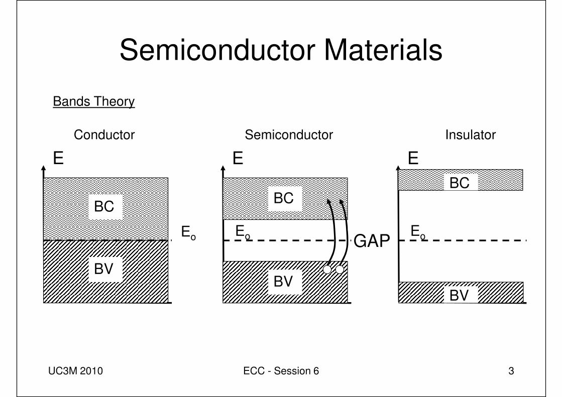
Semiconductor Materials
Conductor InsulatorSemiconductor
Bands Theory
Eo
BC
BV
E
Eo
BC
E
Conductor Insulator
GAPEo
BC
E
Semiconductor
BV
BVBV
UC3M 2010 3ECC - Session 6

Basic Semiconductor Concepts
Intrinsic semiconductor. Electron -hole pair
ni2(T)=n·p n=p (intrinsic) [ ]hee pnq µµρσ ⋅+⋅== /1 [ ]hee pnq µµρσ ⋅+⋅== /1
1,1eVEo
BC
E
Semiconductor
1,1eVEo
BV
UC3M 2010 4ECC - Session 6

Intrinsic Semiconductors (Si)T=0ºK (thermal equilibrium)
+4
-
-
-
-
- -
+4
-
-
-
-+4
-
-
-
-
-
Covalent bond
+4
-
-- +4
-
--+4
-
--
+4
-
-
-
- +4
-
-
-
-+4
-
-
-
-
Free
T > 0ºK
UC3M 2010 5ECC - Session 6
-
+4
-
-
-
- +4
-
-
-
-
--
+4
-
-
-
-
Covalent bond
broken+
Free
electron
(e-)
Free hole(h+)

Semiconductor Currents• DIFFUSION: If free electrons concentration is made higher in one part of the piece of Si than in
another, then the electrons will diffuse from the region of high concentration to the region of low
concentration⇒diffusion current density(Jd [A/cm2])
dx
dpDq
dx
dnDqJJJ pndpdnd ••−••=+=
• DRIFT: An electric (E [V/cm2 ) field is applied]• DRIFT: An electric (E [V/cm2 ) field is applied]
+4
-
-
-
-
--
+4
-
-
-
-+4
-
-
-
-
-
e-
+
+ -E
+
Two charge carriers:
e- and h+
UC3M 2010 6ECC - Session 6
+4
-
-- +4
-
-
-
-+4
-
-
-
-
++h+
Current
EpqEnqJJJ pnapana µµ ••+•••=+=
e- and h+

n-type: Donor impurity atoms. Example: Phosphorus(P).
Extrinsic Semiconductors
+4
-
-
-
-
- -
+4
-
-
-
-+4
-
-
-
-
- -
Free e- ni2(T) = n·p
n > p (n-type)
UC3M 20107
ECC - Session 6
+4
-
-- +5
-
--+4
-
-
-
-
-e- : mayority carriers
h+ : minority carriers

Extrinsic Semiconductors
p- type: Acceptor impurity atoms. Example: Boron (B)
+4
-
-
-
-
-
+4
-
-
-
-+4
-
-
-
-
- +
Free h+
ni2(T) = n·p
p > n (p-type)
h+ : mayority carriers
UC3M 2010 8ECC - Session 6
+4
-
-- +3
-
--+4
-
--
+h+ : mayority carriers
e- : minority carriers

+p n-p-n Junction
equilibrium
Depletion or space charge region (without free carriers)
0
+ -
0
x
Charge density (ρρρρ)
x
Electric field (E)
Potential (V)
UC3M 2010 9ECC - Session 6
x
Potential (V)
Barrier voltage ( Vγγγγ )

-+
Foward bias
+ -
Vd
)1( −= t
d
nV
v
Sd eIi
• id: Mayority carriers current
+p n-id
Reverse bias
+-
Vd
Biased p-n
Juntion
+p n-
+-
id =-Is
UC3M 2010 10ECC - Session 6
-+ • id: Minority carriers current

p n
Anode Cathode
-
id
v
Symbol
The p-n
Junction Diode
Forward
Breakdown
id
vd
-Vbreak
)1( −= t
d
nV
v
Sd eIi
+ -vd
Package
Anode Cathode
I-V CAHARACTERISTIC
q
KTV t =
Reverse
BreakdownVγγγγ = 0.7V ( Si)
vd
-Is = Reverse bias
saturation current
0.5V
UC3M 2010 11ECC - Session 6

Diodes and Applications
SKILLSSKILLS
• To know the diode basic work as a circuit
component and to know the diode models
• To understand the conduction threshold and its use in diode circuits
• To know the types of diode circuits• To know the types of diode circuits
UC3M 2010 12ECC - Session 6

Ideal Diode
idA C
Equivalent Circuit
vD
ON
OFF
A C
vd=0
id>0
A C
Equivalent Circuit
Short Circuit
A C
UC3M 2010 13ECC - Session 6
A C
id=0
vd<0
Open Circuit
A CON
A C
OFF A C

Example: Half-Wave Rectifier
t[ms]
v2(t)
V2p
10 20
f = 50Hz
T = 20ms
0
Secondary winding voltage
-V2p
vO(t)
Vop=V2P
f = 50Hz
T = 20ms
0
D ON Output waveform
V2(t) > 0
V2(t) < 0
Vo(t) = V2(t)
Transfer function
t[ms]
vO
v2
UC3M 2010 14ECC - Session 6
10 200
D OFF
V2(t)>0 V2(t)<0
V2(t) < 0
D ON
D OFF
Vo(t) = 0
0

Diode Equivalent Circuits
1ª Approximation: Ideal Diode
id Equivalent
Circuitid
Equivalent
Circuit
A C
2ª Approximation 3ª Approximation
id
Equivalent
Circuit
A Crd
vd
ON
OFF
A
<
C
vd=0
id>0
Equivalent
Circuit
vd
ON
OFF
Vγγγγ
vd=Vγγγγ
id>0
+ -Vγγγγ
Equivalent
Circuit
vd
ON
OFF
Vγγγγ
vd=Vγγγγ+rd.id
id>0
A C
+ -Vγγγγ
Equivalent
Circuit
1/rd
UC3M 2010 15ECC - Session 6
A C
id=0
vd<0
A C
id=0
vd<Vγγγγ
A C
id=0
vd<Vγγγγ
Circuit

Rectifier Circuits
t[ms]
v2(t)
V2p f = 50Hz
T = 20ms
Secondary winding voltgage
-V2p
10 200
vO(t)
Vop=V2P- Vγγγγ
f = 50Hz
T = 20ms
D ON Output waveform
V2(t) > Vγγγγ
Vo(t) = V2(t) -Vγγγγ
Transfer function
vO
2ª Approximation
UC3M 2010 16ECC - Session 6
10 200
D OFF
V2(t) < Vγγγγ
D ON
D OFF
Vo(t) = 0
Vγγγγ
t[ms] v2
V2(t) < VγγγγV2(t) > Vγγγγ

Limiter Circuits
Vγγγγ
Vo
Transfer function
Vo = Vγγγγ
D ON
Vi > Vγγγγ
Vi < Vγγγγ
Vγγγγ
Vi
D OND OFF
Pendiente =1
Output waveformv
vi(t)
UC3M 2010 17ECC - Session 6
Vo = Vi
D OFF
i
t
Vγγγγ
vo(t)