Serial LVDS High-Speed ADC Interface - Xilinx · The associated reference design illustrates a...
21
XAPP524 (v1.1) November 20, 2012 www.xilinx.com 1 © Copyright 2012 Xilinx, Inc. Xilinx, the Xilinx logo, Artix, ISE, Kintex, Spartan, Virtex, Vivado, Zynq, and other designated brands included herein are trademarks of Xilinx in the United States and other countries. All other trademarks are the property of their respective owners. Summary This application note describes a method of utilizing dedicated SelectIO™ technology deserializer components (ISERDESE2 primitives) in 7 series FPGAs to interface with analog-to-digital converters (ADC) with serial, low-voltage, differential signalling (LVDS) outputs. The associated reference design illustrates a basic LVDS interface connecting a Kintex™-7 FPGA to an ADC with high-speed, serial LVDS outputs. Introduction The high-speed ADCs used today have a resolution of 12, 14, or 16 bits with possible multiple converters in a single package. Each of the converters in the package can be used in standalone mode or converters in the package can be combined and used in an interleaved mode to double or quadruple the conversion (sample) speed. In both standalone mode or interleaved mode, one or two physical serial outputs can be used as a connection to the interfacing device. One set of differential outputs is called a data lane. Using one data lane means that the converter is used in 1-wire mode and two data lanes are called 2-wire mode. For every possible data output combination there is always one high-speed bit clock and one sample rate frame clock available. The 1-wire mode is used in SDR and DDR configurations and 2-wire mode uses only DDR mode. The 1-wire mode keeps the amount of interconnections low and uses normally one data lane per converter in a package. Secondly, the 1-wire mode can be used to output data of one or two converters in an interleaved format. Example of two converters using a 1-wire setup: • One converter outputs data on the rising edge of the bit clock and the second converter uses the falling clock edge. • This immediately doubles the bit clock rate and is therefore not much used. The 2-wire mode doubles the amount of connections between the ADC and interfacing device, but has the great advantage to divide the bit clock by two. A single converter can double the sample clock rate while the bit clock doesn't change frequency or a converter can keep its sample clock rate while the bit clock gets divided by two. In both cases the data is output in interleaved format over two data lanes. The FPGA’s SelectIO technology deserializer components are configured as ISERDESE2 primitives. Two ISERDESE2s in single data rate (SDR) mode are used to capture a double data rate (DDR) signal. One ISERDESE2 is clocked at the rising edge and the second at the falling edge of the bit clock (CLK). This method allows capturing up to 16 bits, each ISERDESE2 can capture 8 bits. Application Note: 7 Series FPGAs XAPP524 (v1.1) November 20, 2012 Serial LVDS High-Speed ADC Interface Author: Marc Defossez
Transcript of Serial LVDS High-Speed ADC Interface - Xilinx · The associated reference design illustrates a...
XAPP524 (v1.1) November 20, 2012 www.xilinx.com 1
© Copyright 2012 Xilinx, Inc. Xilinx, the Xilinx logo, Artix, ISE, Kintex, Spartan, Virtex, Vivado, Zynq, and other designated brands included herein are trademarks of Xilinx in the United States and other countries. All other trademarks are the property of their respective owners.
Summary This application note describes a method of utilizing dedicated SelectIO™ technology deserializer components (ISERDESE2 primitives) in 7 series FPGAs to interface with analog-to-digital converters (ADC) with serial, low-voltage, differential signalling (LVDS) outputs.
The associated reference design illustrates a basic LVDS interface connecting a Kintex™-7 FPGA to an ADC with high-speed, serial LVDS outputs.
Introduction The high-speed ADCs used today have a resolution of 12, 14, or 16 bits with possible multiple converters in a single package. Each of the converters in the package can be used in standalone mode or converters in the package can be combined and used in an interleaved mode to double or quadruple the conversion (sample) speed.
In both standalone mode or interleaved mode, one or two physical serial outputs can be used as a connection to the interfacing device. One set of differential outputs is called a data lane. Using one data lane means that the converter is used in 1-wire mode and two data lanes are called 2-wire mode. For every possible data output combination there is always one high-speed bit clock and one sample rate frame clock available.
The 1-wire mode is used in SDR and DDR configurations and 2-wire mode uses only DDR mode.
The 1-wire mode keeps the amount of interconnections low and uses normally one data lane per converter in a package. Secondly, the 1-wire mode can be used to output data of one or two converters in an interleaved format.
Example of two converters using a 1-wire setup:
• One converter outputs data on the rising edge of the bit clock and the second converter uses the falling clock edge.
• This immediately doubles the bit clock rate and is therefore not much used.
The 2-wire mode doubles the amount of connections between the ADC and interfacing device, but has the great advantage to divide the bit clock by two.
A single converter can double the sample clock rate while the bit clock doesn't change frequency or a converter can keep its sample clock rate while the bit clock gets divided by two. In both cases the data is output in interleaved format over two data lanes.
The FPGA’s SelectIO technology deserializer components are configured as ISERDESE2 primitives. Two ISERDESE2s in single data rate (SDR) mode are used to capture a double data rate (DDR) signal. One ISERDESE2 is clocked at the rising edge and the second at the falling edge of the bit clock (CLK). This method allows capturing up to 16 bits, each ISERDESE2 can capture 8 bits.
Application Note: 7 Series FPGAs
XAPP524 (v1.1) November 20, 2012
Serial LVDS High-Speed ADC InterfaceAuthor: Marc Defossez
FPGA Resources
XAPP524 (v1.1) November 20, 2012 www.xilinx.com 2
FPGA Resources
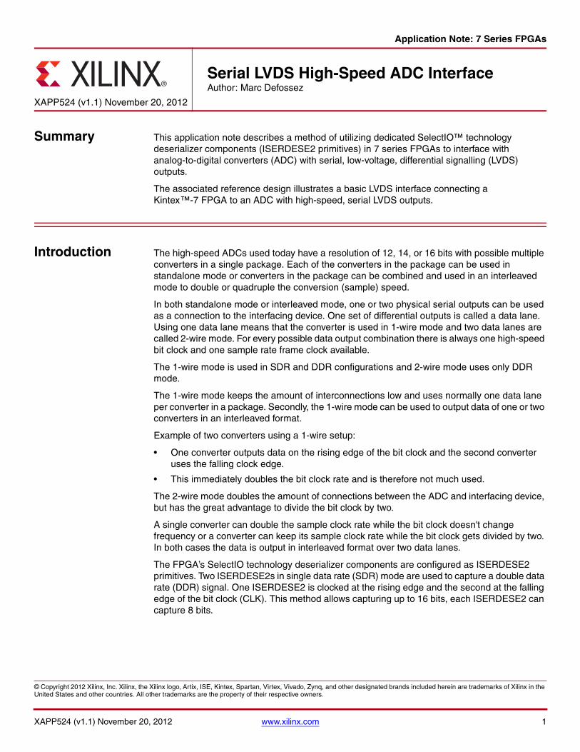
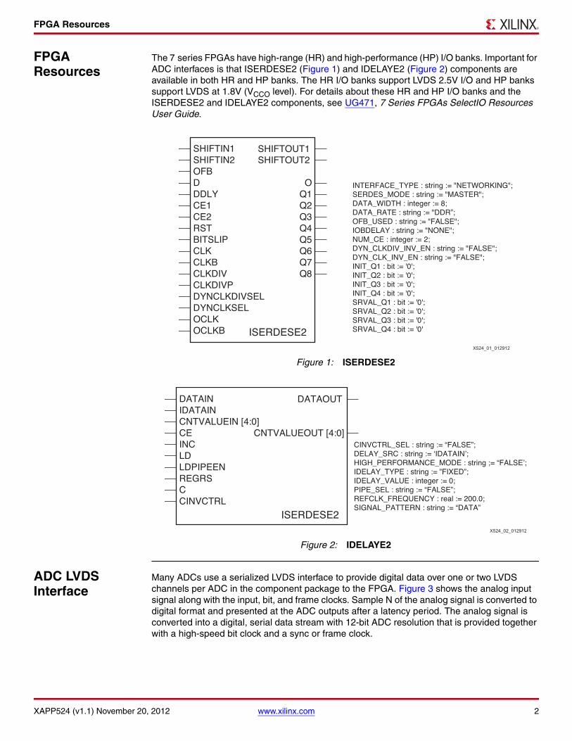
The 7 series FPGAs have high-range (HR) and high-performance (HP) I/O banks. Important for ADC interfaces is that ISERDESE2 (Figure 1) and IDELAYE2 (Figure 2) components are available in both HR and HP banks. The HR I/O banks support LVDS 2.5V I/O and HP banks support LVDS at 1.8V (VCCO level). For details about these HR and HP I/O banks and the ISERDESE2 and IDELAYE2 components, see UG471, 7 Series FPGAs SelectIO Resources User Guide.
ADC LVDS Interface
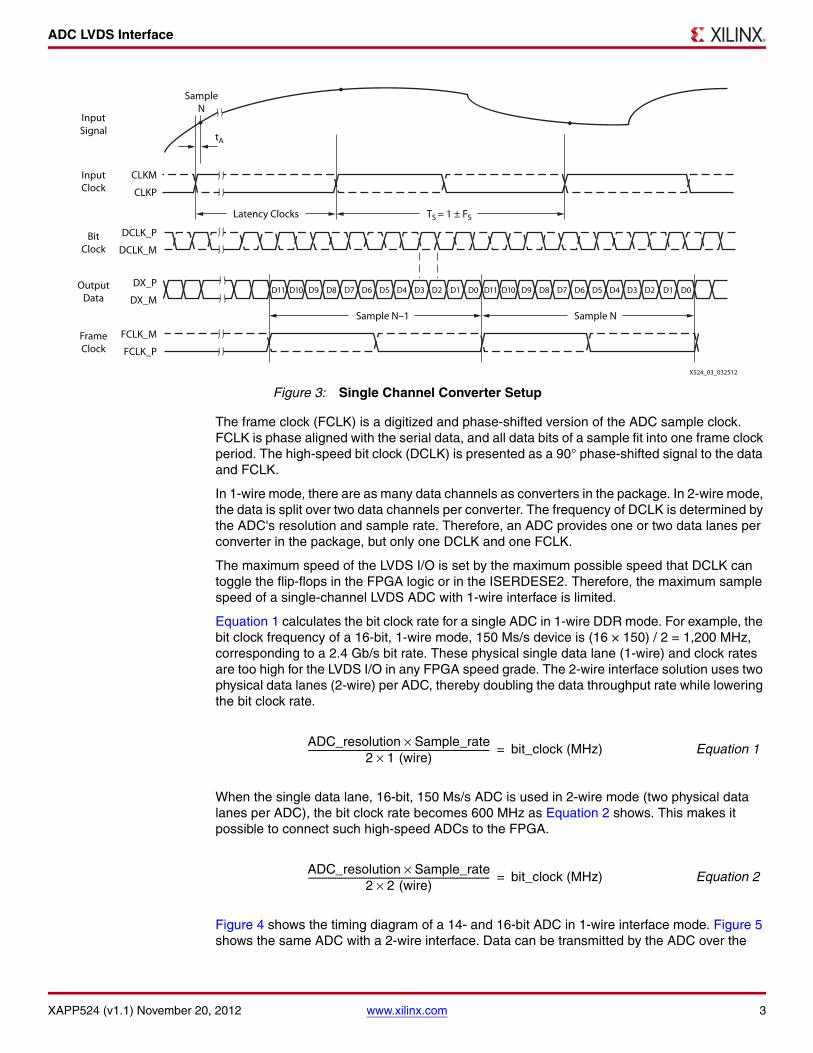
Many ADCs use a serialized LVDS interface to provide digital data over one or two LVDS channels per ADC in the component package to the FPGA. Figure 3 shows the analog input signal along with the input, bit, and frame clocks. Sample N of the analog signal is converted to digital format and presented at the ADC outputs after a latency period. The analog signal is converted into a digital, serial data stream with 12-bit ADC resolution that is provided together with a high-speed bit clock and a sync or frame clock.
X-Ref Target - Figure 1
Figure 1: ISERDESE2
X-Ref Target - Figure 2
Figure 2: IDELAYE2
INTERFACE_TYPE : string := "NETWORKING";SERDES_MODE : string := "MASTER";DATA_WIDTH : integer := 8;DATA_RATE : string := "DDR”;OFB_USED : string := "FALSE";IOBDELAY : string := "NONE";NUM_CE : integer := 2;DYN_CLKDIV_INV_EN : string := "FALSE";DYN_CLK_INV_EN : string := "FALSE";INIT_Q1 : bit := '0';INIT_Q2 : bit := '0';INIT_Q3 : bit := '0';INIT_Q4 : bit := '0';SRVAL_Q1 : bit := '0';SRVAL_Q2 : bit := '0';SRVAL_Q3 : bit := '0';SRVAL_Q4 : bit := '0'ISERDESE2
SHIFTIN1SHIFTIN2OFBDDDLYCE1CE2RSTBITSLIPCLKCLKBCLKDIVCLKDIVPDYNCLKDIVSELDYNCLKSELOCLKOCLKB
OQ1Q2Q3Q4Q5Q6Q7Q8
SHIFTOUT1SHIFTOUT2
X524_01_012912
CINVCTRL_SEL : string := “FALSE”;DELAY_SRC : string := ‘IDATAIN’;HIGH_PERFORMANCE_MODE : string ;= “FALSE’;IDELAY_TYPE : string := ”FIXED”;IDELAY_VALUE : integer := 0;PIPE_SEL : string := “FALSE”;REFCLK_FREQUENCY : real := 200.0;SIGNAL_PATTERN : string := “DATA”
ISERDESE2
DATAINIDATAINCNTVALUEIN [4:0]CEINCLDLDPIPEENREGRSCCINVCTRL
CNTVALUEOUT [4:0]
DATAOUT
X524_02_012912
ADC LVDS Interface
XAPP524 (v1.1) November 20, 2012 www.xilinx.com 3
The frame clock (FCLK) is a digitized and phase-shifted version of the ADC sample clock. FCLK is phase aligned with the serial data, and all data bits of a sample fit into one frame clock period. The high-speed bit clock (DCLK) is presented as a 90° phase-shifted signal to the data and FCLK.
In 1-wire mode, there are as many data channels as converters in the package. In 2-wire mode, the data is split over two data channels per converter. The frequency of DCLK is determined by the ADC's resolution and sample rate. Therefore, an ADC provides one or two data lanes per converter in the package, but only one DCLK and one FCLK.
The maximum speed of the LVDS I/O is set by the maximum possible speed that DCLK can toggle the flip-flops in the FPGA logic or in the ISERDESE2. Therefore, the maximum sample speed of a single-channel LVDS ADC with 1-wire interface is limited.
Equation 1 calculates the bit clock rate for a single ADC in 1-wire DDR mode. For example, the bit clock frequency of a 16-bit, 1-wire mode, 150 Ms/s device is (16 × 150) / 2 = 1,200 MHz, corresponding to a 2.4 Gb/s bit rate. These physical single data lane (1-wire) and clock rates are too high for the LVDS I/O in any FPGA speed grade. The 2-wire interface solution uses two physical data lanes (2-wire) per ADC, thereby doubling the data throughput rate while lowering the bit clock rate.
Equation 1
When the single data lane, 16-bit, 150 Ms/s ADC is used in 2-wire mode (two physical data lanes per ADC), the bit clock rate becomes 600 MHz as Equation 2 shows. This makes it possible to connect such high-speed ADCs to the FPGA.
Equation 2
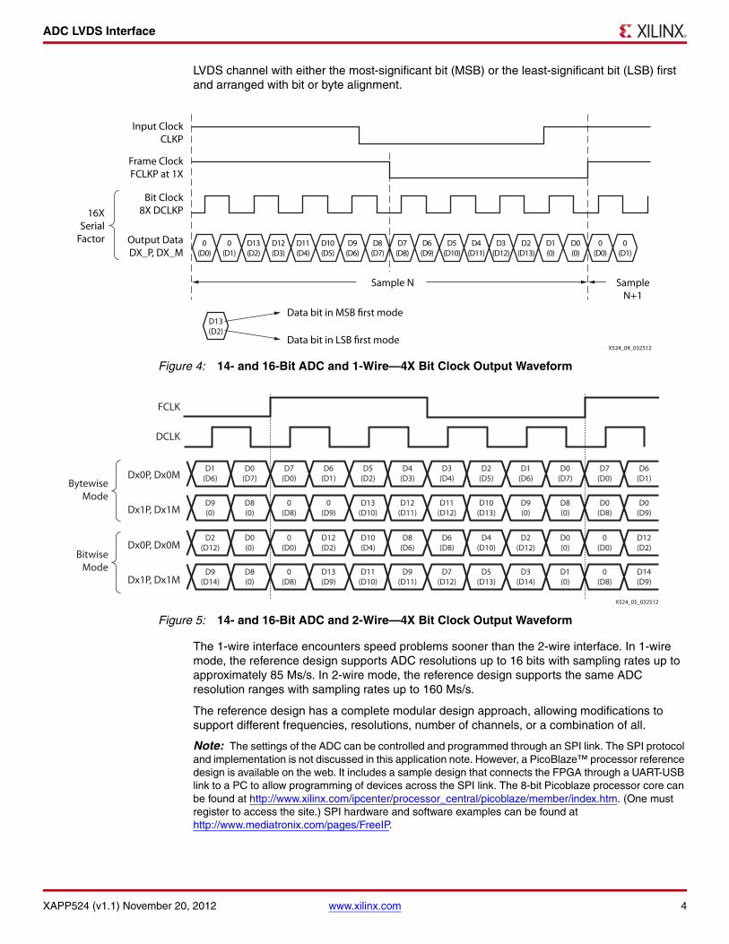
Figure 4 shows the timing diagram of a 14- and 16-bit ADC in 1-wire interface mode. Figure 5 shows the same ADC with a 2-wire interface. Data can be transmitted by the ADC over the
X-Ref Target - Figure 3
Figure 3: Single Channel Converter Setup
SampleN
X524_03_032512
InputSignal
InputClock
CLKM
Latency Clocks
Sample N–1 Sample N
D11 D10 D9 D8 D7 D6 D5 D4 D3 D2 D1 D0 D9 D8 D7 D6 D5 D4 D3 D2 D1 D0D11 D10
TS = 1 ± FS
CLKP
FCLK_M
FCLK_P
DCLK_P
DCLK_M
DX_P
DX_M
BitClock
FrameClock
OutputData
tA
ADC_resolution Sample_rate×2 1 (wire)×
---------------------------------------------------------------------------------- bit_clock (MHz)=
ADC_resolution Sample_rate×2 2 (wire)×
---------------------------------------------------------------------------------- bit_clock (MHz)=
ADC LVDS Interface
XAPP524 (v1.1) November 20, 2012 www.xilinx.com 4
LVDS channel with either the most-significant bit (MSB) or the least-significant bit (LSB) first and arranged with bit or byte alignment.
The 1-wire interface encounters speed problems sooner than the 2-wire interface. In 1-wire mode, the reference design supports ADC resolutions up to 16 bits with sampling rates up to approximately 85 Ms/s. In 2-wire mode, the reference design supports the same ADC resolution ranges with sampling rates up to 160 Ms/s.
The reference design has a complete modular design approach, allowing modifications to support different frequencies, resolutions, number of channels, or a combination of all.
Note: The settings of the ADC can be controlled and programmed through an SPI link. The SPI protocol and implementation is not discussed in this application note. However, a PicoBlaze™ processor reference design is available on the web. It includes a sample design that connects the FPGA through a UART-USB link to a PC to allow programming of devices across the SPI link. The 8-bit Picoblaze processor core can be found at http://www.xilinx.com/ipcenter/processor_central/picoblaze/member/index.htm. (One must register to access the site.) SPI hardware and software examples can be found at http://www.mediatronix.com/pages/FreeIP.
X-Ref Target - Figure 4
Figure 4: 14- and 16-Bit ADC and 1-Wire—4X Bit Clock Output Waveform
Sample N
Data bit in MSB first mode
Data bit in LSB first mode
Input ClockCLKP
Frame ClockFCLKP at 1X
Bit Clock8X DCLKP16X
SerialFactor Output Data
DX_P, DX_MD12(D3)
D11(D4)
D10(D5)
D9(D6)
D8(D7)
D7(D8)
D6(D9)
D5(D10)
D4(D11)
D3(D12)
D2(D13)
D1(0)
D0(0)
0(D0)
0(D1)
D13(D2)
D13(D2)
0(D1)
0(D0)
SampleN+1
X524_04_032512
X-Ref Target - Figure 5
Figure 5: 14- and 16-Bit ADC and 2-Wire—4X Bit Clock Output Waveform
X524_05_032512
FCLK
DCLK
Dx0P, Dx0MBytewise
Mode
BitwiseMode
Dx1P, Dx1M
Dx0P, Dx0M
Dx1P, Dx1MD3
(D14)D9
(D14)D5
(D13)D7
(D12)D9
(D11)D11
(D10)D13(D9)
D8(0)
D1(0)
0(D8)
0(D8)
D14(D9)
D1(D6)
D1(D6)
D2(D5)
D3(D4)
D4(D3)
D5(D2)
D6(D1)
D0(D7)
D0(D7)
D7(D0)
D7(D0)
D6(D1)
D9(0)
D9(0)
D10(D13)
D11(D12)
D12(D11)
D13(D10)
0(D9)
D8(0)
D8(0)
D0(D8)
0(D8)
D0(D9)
D2(D12)
D2(D12)
D4(D10)
D6(D8)
D8(D6)
D10(D4)
D12(D2)
D0(0)
D0(0)
0(D0)
0(D0)
D12(D2)

Bit Clock
XAPP524 (v1.1) November 20, 2012 www.xilinx.com 5
Bit Clock The bit clock rate is determined by Equation 1. For a 16-bit, 200 Ms/s ADC, 1-wire ADC, the DDR bit clock rate is 1,600 MHz.
Note: In Equation 1, to determine Sample Rate from Adc_resolution and Bit_Clock, the Wire_Interface must be set to 2 for an ADC used in 2-wire mode and 1 for a 1-wire mode operated ADC.
The 1-wire ADC bit clock rate is too fast for the 7 series FPGAs clock-capable inputs and the regional clock trees used in this design. Therefore, the ADC must be used in 2-wire mode. In 2-wire mode, the ADC data is distributed over two LVDS channels per converter, which means that the bit clock is divided by two. For example, for a 16-bit, 200 Ms/s converter, 2-wire ADC, the bit clock rate is 800 MHz.
Table 1 provides examples of the relationship between the wire interface, the bit clock based on the ADC resolution, and sample clock parameters. Equation 1 is an easy way to calculate values from known parameters.
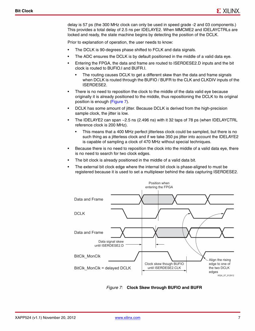
The bit clock provided by the ADC is 90° out-of-phase with respect to the data and frame signals. The designer must maintain this alignment all the way to the FPGA using good PCB layout techniques because the delay from the package-pad to the D input of each ISERDESE2 is equal for all signals.
Due to routing and clock buffer delay inside the FPGA grid, DCLK must be repositioned for capturing data and frame signals, as shown in Figure 6.
Table 1: ADC Parameter Relationship
Resolution (Bits)
Sample Rate (MHz)
Interface Type
Bit Clock(MHz) Comments
1280 1-wire 480 OK
125 2-wire 375 OK
14125 1-wire 875 Not OK. 2-wire mode needed.
150 2-wire 525 OK
16125 2-wire 500 OK
200 2-wire 800 OK. Needs the fastest speed grade.
Notes: ADCs with a 14-bit resolution often run in a 16-bit output mode. Two data bits are dummy bits or used to indicate overflow. The calculation of clock rates must then be carried using 16 bits as the resolution parameter.
Bit Clock
XAPP524 (v1.1) November 20, 2012 www.xilinx.com 6
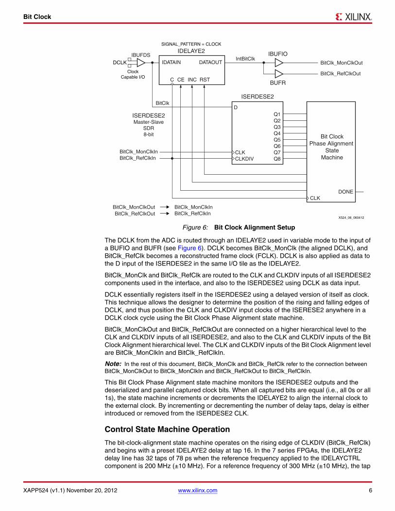
The DCLK from the ADC is routed through an IDELAYE2 used in variable mode to the input of a BUFIO and BUFR (see Figure 6). DCLK becomes BitClk_MonClk (the aligned DCLK), and BitClk_RefClk becomes a reconstructed frame clock (FCLK). DCLK is also applied as data to the D input of the ISERDESE2 in the same I/O tile as the IDELAYE2.
BitClk_MonClk and BitClk_RefClk are routed to the CLK and CLKDIV inputs of all ISERDESE2 components used in the interface, and also to the ISERDESE2 using DCLK as data input.
DCLK essentially registers itself in the ISERDESE2 using a delayed version of itself as clock. This technique allows the designer to determine the position of the rising and falling edges of DCLK, and thus position the CLK and CLKDIV input clocks of the ISERESE2 anywhere in a DCLK clock cycle using the Bit Clock Phase Alignment state machine.
BitClk_MonClkOut and BitClk_RefClkOut are connected on a higher hierarchical level to the CLK and CLKDIV inputs of all ISERDESE2, and also to the CLK and CLKDIV inputs of the Bit Clock Alignment hierarchical level. The CLK and CLKDIV inputs of the Bit Clock Alignment level are BitClk_MonClkIn and BitClk_RefClkIn.
Note: In the rest of this document, BitClk_MonClk and BitClk_RefClk refer to the connection between BitClk_MonClkOut to BitClk_MonClkIn and BitClk_RefClkOut to BitClk_RefClkIn.
This Bit Clock Phase Alignment state machine monitors the ISERDESE2 outputs and the deserialized and parallel captured clock bits. When all captured bits are equal (i.e., all 0s or all 1s), the state machine increments or decrements the IDELAYE2 to align the internal clock to the external clock. By incrementing or decrementing the number of delay taps, delay is either introduced or removed from the ISERDESE2 CLK.
Control State Machine Operation
The bit-clock-alignment state machine operates on the rising edge of CLKDIV (BitClk_RefClk) and begins with a preset IDELAYE2 delay at tap 16. In the 7 series FPGAs, the IDELAYE2 delay line has 32 taps of 78 ps when the reference frequency applied to the IDELAYCTRL component is 200 MHz (±10 MHz). For a reference frequency of 300 MHz (±10 MHz), the tap
X-Ref Target - Figure 6
Figure 6: Bit Clock Alignment Setup
IBUFDSIDATAIN
D
CLKCLKDIV
BitClk_MonClkOutIntBitClk
BitClk
Master-SlaveSDR8-bit
BitClk_RefClkOut
Q7 Q8
Q6
CLKDONE
Q5Q4Q3Q2Q1
DATAOUT
RST INC CE C
BitClk_MonClkInBitClk_RefClkIn
BitClk_MonClkOutBitClk_RefClkOut
BitClk_MonClkInBitClk_RefClkIn
X524_06_060412
IDELAYE2
ISERDESE2
ISERDESE2
IBUFIO
BUFR
Bit ClockPhase Alignment
StateMachine
ClockCapable I/O
SIGNAL_PATTERN = CLOCK
DCLK
Bit Clock
XAPP524 (v1.1) November 20, 2012 www.xilinx.com 7
delay is 57 ps (the 300 MHz clock can only be used in speed grade -2 and 03 components.) This provides a total delay of 2.5 ns per IDELAYE2. When MMCME2 and IDELAYCTRLs are locked and ready, the state machine begins by detecting the position of the DCLK.
Prior to explanation of operation, the user needs to know:
• The DCLK is 90-degrees phase shifted to FCLK and data signals.
• The ADC ensures the DCLK is by default positioned in the middle of a valid data eye.
• Entering the FPGA, the data and frame are routed to ISERDESE2.D inputs and the bit clock is routed to BUFIO.I and BUFR.I.
• The routing causes DCLK to get a different skew than the data and frame signals when DCLK is routed through the BUFIO / BUFR to the CLK and CLKDIV inputs of the ISERDESE2.
• There is no need to reposition the clock to the middle of the data valid eye because originally it is already positioned to the middle, thus repositioning the DCLK to its original position is enough (Figure 7).
• DCLK has some amount of jitter. Because DCLK is derived from the high-precision sample clock, the jitter is low.
• The IDELAYE2 can span ~2.5 ns (2.496 ns) with it 32 taps of 78 ps (when IDELAYCTRL reference clock is 200 MHz).
• This means that a 400 MHz perfect jitterless clock could be sampled, but there is no such thing as a jitterless clock and if we take 350 ps jitter into account the IDELAYE2 is capable of sampling a clock of 470 MHz without special techniques.
• Because there is no need to reposition the clock into the middle of a valid data eye, there is no need to search for two clock edges.
• The bit clock is already positioned in the middle of a valid data bit.
• The external bit clock edge where the internal bit clock is phase-aligned to must be registered because it is used to set a multiplexer behind the data capturing ISERDESE2.
X-Ref Target - Figure 7
Figure 7: Clock Skew through BUFIO and BUFR
DCLK
Position whenentering the FPGA
Data signal skewuntil ISERDESE2.D
Data and Frame
Data and Frame
BitClk_MonClk
Clock skew though BUFIOuntil ISERDESE2.CLK
X524_07_012912
BitClk_MonClk = delayed DCLK
Align the risingedge to one ofthe two DCLKedges
Bit Clock
XAPP524 (v1.1) November 20, 2012 www.xilinx.com 8
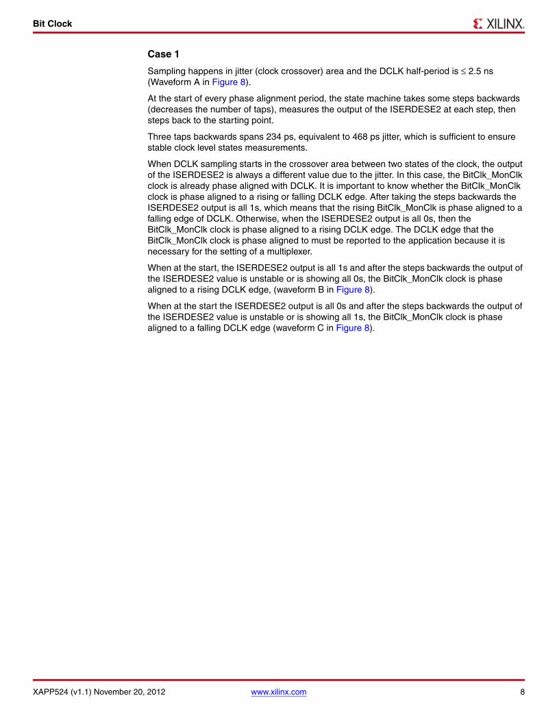
Case 1
Sampling happens in jitter (clock crossover) area and the DCLK half-period is ≤ 2.5 ns (Waveform A in Figure 8).
At the start of every phase alignment period, the state machine takes some steps backwards (decreases the number of taps), measures the output of the ISERDESE2 at each step, then steps back to the starting point.
Three taps backwards spans 234 ps, equivalent to 468 ps jitter, which is sufficient to ensure stable clock level states measurements.
When DCLK sampling starts in the crossover area between two states of the clock, the output of the ISERDESE2 is always a different value due to the jitter. In this case, the BitClk_MonClk clock is already phase aligned with DCLK. It is important to know whether the BitClk_MonClk clock is phase aligned to a rising or falling DCLK edge. After taking the steps backwards the ISERDESE2 output is all 1s, which means that the rising BitClk_MonClk is phase aligned to a falling edge of DCLK. Otherwise, when the ISERDESE2 output is all 0s, then the BitClk_MonClk clock is phase aligned to a rising DCLK edge. The DCLK edge that the BitClk_MonClk clock is phase aligned to must be reported to the application because it is necessary for the setting of a multiplexer.
When at the start, the ISERDESE2 output is all 1s and after the steps backwards the output of the ISERDESE2 value is unstable or is showing all 0s, the BitClk_MonClk clock is phase aligned to a rising DCLK edge, (waveform B in Figure 8).
When at the start the ISERDESE2 output is all 0s and after the steps backwards the output of the ISERDESE2 value is unstable or is showing all 1s, the BitClk_MonClk clock is phase aligned to a falling DCLK edge (waveform C in Figure 8).
Bit Clock
XAPP524 (v1.1) November 20, 2012 www.xilinx.com 9
Waveform D in Figure 8 shows the opposite of the waveform C in Figure 8. The output is initially stable at 1 and after the first steps backward the output is unstable or all 0s, showing that a rising edge is detected.
The IDELAYE2 cannot be stepped to its original starting position because at the start DCLK and BitClk_MonClk are not exactly phase aligned.
X-Ref Target - Figure 8
Figure 8: Sample Edge Directly Detected (A, B, C, and D)
DCLK
C)
BitClk_MonClk
X524_08C_030212
Sample on therising edge
Start
16
13
-3 tapsFrom Q[8:1] stable at 0 toQ[8:1] unstable or stable at 1.Falling edge found
1
DCLK
B)
BitClk_MonClk
X524_08B_030212
Start
1613
-3 tapsFrom Q[8:1] unstable toQ[8:1] stable at 1.Falling edge found
Sample on the rising edge1
BitClk_MonClk
DCLK
D)
X524_08D_030212
Sample on the rising edge
Start
1613
-3 tapsFrom Q[8:1] stable at 1 to Q[8:1] unstable or stable at 0.Rising edge found
1
BitClk_MonClk
DCLK
A) Start
16
13X524_08A_030212
-3 tapsFrom Q[8:1] unstable toQ[8:1] stable at 0.Rising edge found
Sample on the rising edge1
Bit Clock
XAPP524 (v1.1) November 20, 2012 www.xilinx.com 10
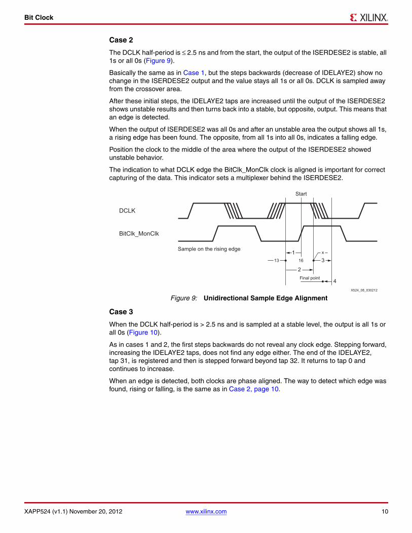
Case 2
The DCLK half-period is ≤ 2.5 ns and from the start, the output of the ISERDESE2 is stable, all 1s or all 0s (Figure 9).
Basically the same as in Case 1, but the steps backwards (decrease of IDELAYE2) show no change in the ISERDESE2 output and the value stays all 1s or all 0s. DCLK is sampled away from the crossover area.
After these initial steps, the IDELAYE2 taps are increased until the output of the ISERDESE2 shows unstable results and then turns back into a stable, but opposite, output. This means that an edge is detected.
When the output of ISERDESE2 was all 0s and after an unstable area the output shows all 1s, a rising edge has been found. The opposite, from all 1s into all 0s, indicates a falling edge.
Position the clock to the middle of the area where the output of the ISERDESE2 showed unstable behavior.
The indication to what DCLK edge the BitClk_MonClk clock is aligned is important for correct capturing of the data. This indicator sets a multiplexer behind the ISERDESE2.
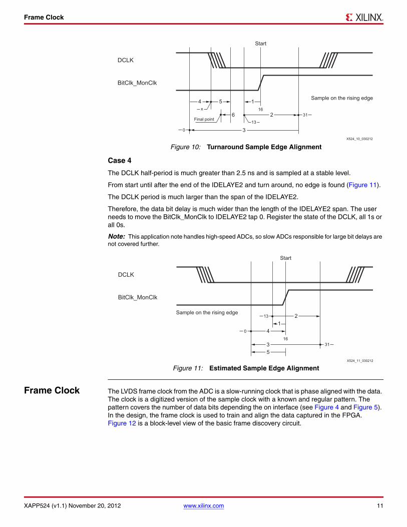
Case 3
When the DCLK half-period is > 2.5 ns and is sampled at a stable level, the output is all 1s or all 0s (Figure 10).
As in cases 1 and 2, the first steps backwards do not reveal any clock edge. Stepping forward, increasing the IDELAYE2 taps, does not find any edge either. The end of the IDELAYE2, tap 31, is registered and then is stepped forward beyond tap 32. It returns to tap 0 and continues to increase.
When an edge is detected, both clocks are phase aligned. The way to detect which edge was found, rising or falling, is the same as in Case 2, page 10.
X-Ref Target - Figure 9
Figure 9: Unidirectional Sample Edge Alignment
BitClk_MonClk
DCLK
X524_08_030212
Sample on the rising edge
Start
16
x113
2
3
4Final point
Frame Clock
XAPP524 (v1.1) November 20, 2012 www.xilinx.com 11
Case 4
The DCLK half-period is much greater than 2.5 ns and is sampled at a stable level.
From start until after the end of the IDELAYE2 and turn around, no edge is found (Figure 11).
The DCLK period is much larger than the span of the IDELAYE2.
Therefore, the data bit delay is much wider than the length of the IDELAYE2 span. The user needs to move the BitClk_MonClk to IDELAYE2 tap 0. Register the state of the DCLK, all 1s or all 0s.
Note: This application note handles high-speed ADCs, so slow ADCs responsible for large bit delays are not covered further.
Frame Clock The LVDS frame clock from the ADC is a slow-running clock that is phase aligned with the data. The clock is a digitized version of the sample clock with a known and regular pattern. The pattern covers the number of data bits depending the on interface (see Figure 4 and Figure 5). In the design, the frame clock is used to train and align the data captured in the FPGA. Figure 12 is a block-level view of the basic frame discovery circuit.
X-Ref Target - Figure 10
Figure 10: Turnaround Sample Edge Alignment
X-Ref Target - Figure 11
Figure 11: Estimated Sample Edge Alignment
BitClk_MonClk
DCLK
X524_10_030212
Sample on the rising edge
Start
16
1
3
6 31
0
2
54x
13Final point
BitClk_MonClk
DCLK
X524_11_030212
Sample on the rising edge
Start
16
1
3
5
31
13
0
2
4

Frame Clock
XAPP524 (v1.1) November 20, 2012 www.xilinx.com 12
Two ISERDESE2 components are used in NETWORKING single data rate (SDR) mode. Each ISERDESE2 is clocked on a different edge of the aligned bit clock (DCLK). The discovery of the frame clock pattern starts when the bit clock (DCLK) is properly aligned.
The output of the two ISERDESE2 is compared to a fixed value representing the expected frame clock pattern. When this fixed value is not equal to the output of the ISERDESE2, a Bitslip operation is initiated for both the frame and all data signals. Bitslips are applied until the output of the frame clock ISERDESE2 components matches the given frame clock pattern. When this output is equal to the programmed pattern value, the Bitslip operation is stopped for both frame clock and the data. The data and frame clock signals within the FPGA are then considered valid. However, the data and frame clock signals are not always valid.
After the execution of a number of Bitslip operations, the construction of the ISERDESE2 allows the output to show the same value as from the preceding cycle. For normal source-synchronous designs, where training patterns are executed in the data, this is not an issue. The only consequence there is that extra Bitslip operations are necessary to achieve synchronization.
In typical ADC interfaces the frame synchronization runs without training pattern, the ISERDESE2 that outputs the same value twice puts the whole synchronization process in jeopardy. Without precautions and when double outputs appear, the frame capturing circuit operates as if it is synchronized to the frame pattern, when in reality it has not!
The result of this erroneous frame synchronization appears in the captured data. The data capturing ISERDESE2 is shifted along with the frame ISERDESE2. Thus, when the frame assumes synchronization at a wrong place, the data values are wrong. Therefore the frame alignment circuit got a double nibble detection state machine to avoid this issue.
Frame Pattern Capturing
The frame clock is captured as a data stream with constant but repeating data pattern. Because the frame channel and data channel are phase-aligned, the frame clock is well suited for use as a training pattern or synchronization lane for the real data lanes. When it is possible
X-Ref Target - Figure 12
Figure 12: Basic Frame Discovery Circuit
RqrdPattern
FrameIn_p
FrameIn_n [15:8]
[7:0]
Register
Register
BitS
lip_p
BitS
lip_n
Captured
Pattern
Sw
apMux
MsbR
egEna
LsbRegE
na
Multiplexer Register
Frame Alignment State Machine
ISERDESE2
ISERDESE2
Register
CLKDIVCLK
X524_12_060712
Frame Clock
XAPP524 (v1.1) November 20, 2012 www.xilinx.com 13
to adjust the captured frame pattern so that it corresponds to a given pattern (i.e., the pattern it normally must have), the received data is ensured to have the correct format.
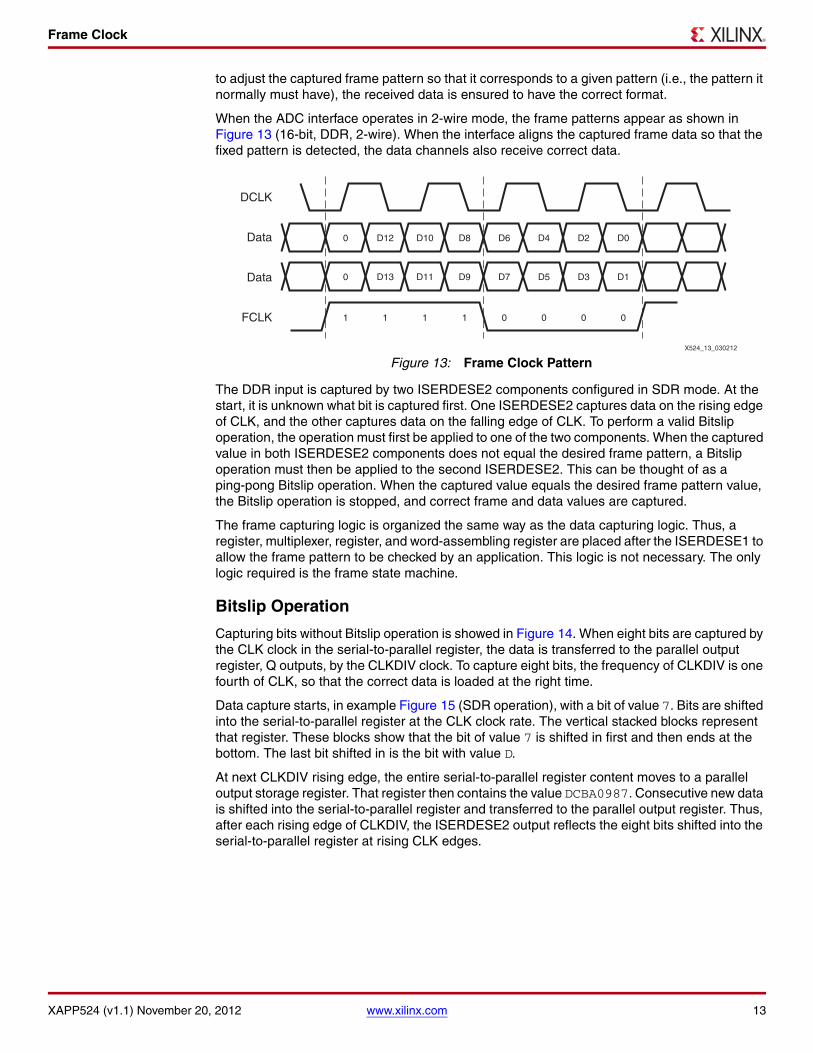
When the ADC interface operates in 2-wire mode, the frame patterns appear as shown in Figure 13 (16-bit, DDR, 2-wire). When the interface aligns the captured frame data so that the fixed pattern is detected, the data channels also receive correct data.
The DDR input is captured by two ISERDESE2 components configured in SDR mode. At the start, it is unknown what bit is captured first. One ISERDESE2 captures data on the rising edge of CLK, and the other captures data on the falling edge of CLK. To perform a valid Bitslip operation, the operation must first be applied to one of the two components. When the captured value in both ISERDESE2 components does not equal the desired frame pattern, a Bitslip operation must then be applied to the second ISERDESE2. This can be thought of as a ping-pong Bitslip operation. When the captured value equals the desired frame pattern value, the Bitslip operation is stopped, and correct frame and data values are captured.
The frame capturing logic is organized the same way as the data capturing logic. Thus, a register, multiplexer, register, and word-assembling register are placed after the ISERDESE1 to allow the frame pattern to be checked by an application. This logic is not necessary. The only logic required is the frame state machine.
Bitslip Operation
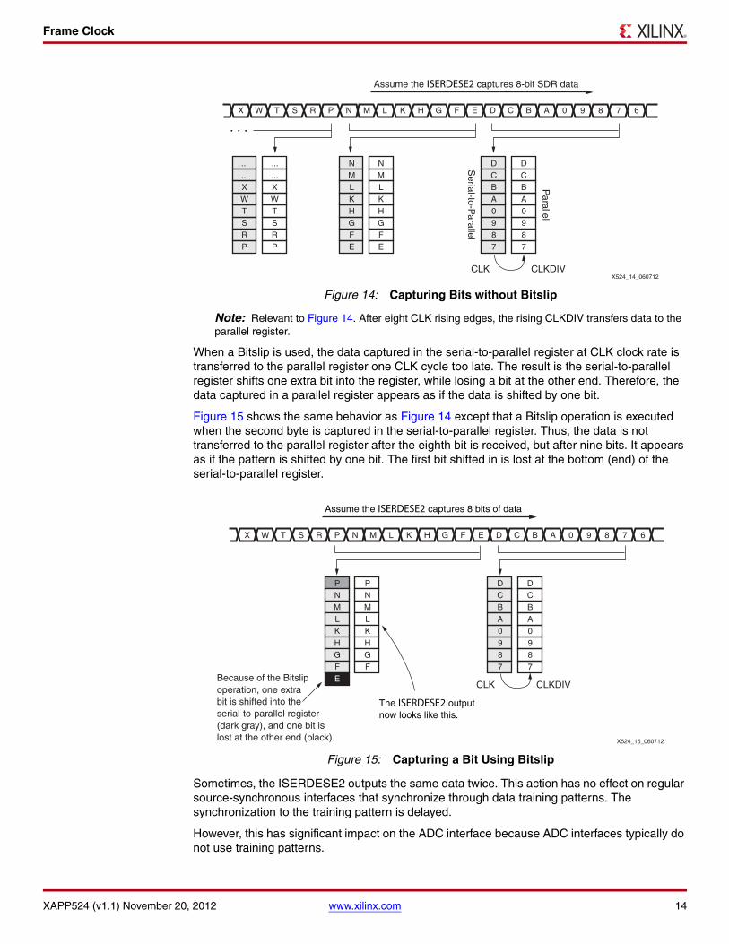
Capturing bits without Bitslip operation is showed in Figure 14. When eight bits are captured by the CLK clock in the serial-to-parallel register, the data is transferred to the parallel output register, Q outputs, by the CLKDIV clock. To capture eight bits, the frequency of CLKDIV is one fourth of CLK, so that the correct data is loaded at the right time.
Data capture starts, in example Figure 15 (SDR operation), with a bit of value 7. Bits are shifted into the serial-to-parallel register at the CLK clock rate. The vertical stacked blocks represent that register. These blocks show that the bit of value 7 is shifted in first and then ends at the bottom. The last bit shifted in is the bit with value D.
At next CLKDIV rising edge, the entire serial-to-parallel register content moves to a parallel output storage register. That register then contains the value DCBA0987. Consecutive new data is shifted into the serial-to-parallel register and transferred to the parallel output register. Thus, after each rising edge of CLKDIV, the ISERDESE2 output reflects the eight bits shifted into the serial-to-parallel register at rising CLK edges.
X-Ref Target - Figure 13
Figure 13: Frame Clock PatternX524_13_030212
DCLK
FCLK
Data
Data
0
0
D12
D13
D10
D11
D8
D9
D6
D7
D4
D5
D2
D3
D0
D1
1 1 1 1 0 0 0 0
Frame Clock
XAPP524 (v1.1) November 20, 2012 www.xilinx.com 14
Note: Relevant to Figure 14. After eight CLK rising edges, the rising CLKDIV transfers data to the parallel register.
When a Bitslip is used, the data captured in the serial-to-parallel register at CLK clock rate is transferred to the parallel register one CLK cycle too late. The result is the serial-to-parallel register shifts one extra bit into the register, while losing a bit at the other end. Therefore, the data captured in a parallel register appears as if the data is shifted by one bit.
Figure 15 shows the same behavior as Figure 14 except that a Bitslip operation is executed when the second byte is captured in the serial-to-parallel register. Thus, the data is not transferred to the parallel register after the eighth bit is received, but after nine bits. It appears as if the pattern is shifted by one bit. The first bit shifted in is lost at the bottom (end) of the serial-to-parallel register.
Sometimes, the ISERDESE2 outputs the same data twice. This action has no effect on regular source-synchronous interfaces that synchronize through data training patterns. The synchronization to the training pattern is delayed.
However, this has significant impact on the ADC interface because ADC interfaces typically do not use training patterns.
X-Ref Target - Figure 14
Figure 14: Capturing Bits without Bitslip
X-Ref Target - Figure 15
Figure 15: Capturing a Bit Using Bitslip
X524_14_060712
X W T S R P N M L K H G F
...
...XWTSRP
...
...XWTSRP
NMLKHGFE
NMLKHGFE
DCBA0987
DCBA0987
Parallel
Serial-to-P
arallel
E D C B A 0 9 8 7 6
Assume the ISERDESE2 captures 8-bit SDR data
CLK CLKDIV
. . .
X524_15_060712
X W T S R P N M L K H G F
PNMLKHGF
PNMLKHGFE
DCBA0987
DCBA0987
E D C B A 0 9 8 7 6
Assume the ISERDESE2 captures 8 bits of data
Because of the Bitslipoperation, one extra bit is shifted into the serial-to-parallel register (dark gray), and one bit is lost at the other end (black).
The ISERDESE2 outputnow looks like this.
CLK CLKDIV

Frame Clock
XAPP524 (v1.1) November 20, 2012 www.xilinx.com 15
The ADC interface is synchronized using the frame clock signal. All other signals and data inputs are shifted along with the frame pattern while it is synchronizing. Therefore, when the frame circuit erroneously assumes it is synchronized to the frame pattern, the captured data is corrupted.
Because the ISERDESE2 Bitslip operation does not occur for both components simultaneously, one can output the same data twice before the other ISERDESE2. Making synchronization is virtually impossible.
These operations are illustrated in Figure 16:
• After a few Bitslip operations, the output of the ISERDESE2 components is 3 and E, resulting in the byte AD.
• 0011_1110 = 1 0 1 0 1 1 0 1
• The next output is C and 1, resulting in a byte 52.
• The ISERDESE2 indicated by “_p” receives a Bitslip request and executes it. The result should be 1 and E, resulting in A9. Instead, the ISERDESE2 outputs C a second time, and the resulting byte is now F8 (C and E). A nibble of the received byte did not receive the Bitslip request when it should have and is delayed one CLKDIV period, resulting in a mixed-up byte.
• On the next CLKDIV edge, the earlier Bitslip operation occurs at the output of the ISERDESE2, resulting in 1 and 1 or 03.
Double Nibble Detect
To counter the earlier discussed effect, where the ISERDESE2 outputs twice the same data and then continues as if nothing happened, a small state machine is developed.
The output data of the ISERDESE2 is passed through a series of registers.
The previous and present output of the ISERDESE2 is compared at the first register, before and after the register.
When the ISERDESE2 outputs twice the same data, the previous and present data will be identical. A comparator in the design performs this function.
When a double nibble is detected, a selection of data is made out of the other registers so that the output of the register bank shows a continuing stream of data.
X-Ref Target - Figure 16
Figure 16: Duplicate Output DataX524_16_032612
FrmClkReSync
/IntFrmSrdsOut_Isrds_p
IntfrmSrdsOut_Isrds_n
IntFrmSrdsOut
IntFrmDat
IntFrmDatSwp
FrmClkDat
IntFrmEqu_d
T X
F 00 3 1 E 1 E 1 E 1 EC
8 70 E 1 1 E 1 F 0 F 0E
D5 2A00 AD 52 03 FC 03 1 AB56 54 AB 5F8
AA 7F00 F8 07 52 A9 56 1 FCA9 01 FE 0F8
AA
00AA
00
0000
07 07 F8 52 1 56A9 A9 FC 01 FF8
O
Start of explication
Data
XAPP524 (v1.1) November 20, 2012 www.xilinx.com 16
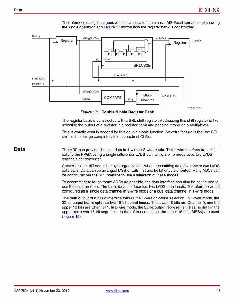
The reference design that goes with this application note has a MS-Excel spreadsheet showing the whole operation and Figure 17 shows how the register bank is constructed.
The register bank is constructed with a SRL shift register. Addressing this shift register is like selecting the output of a register in a register bank and passing it through a multiplexer.
This is exactly what is needed for this double nibble function. An extra feature is that the SRL shrinks the design completely into a couple of CLBs.
Data The ADC can provide digitized data in 1-wire or 2-wire mode. The 1-wire interface transmits data to the FPGA using a single differential LVDS pair, while 2-wire mode uses two LVDS channels per converter.
Converters use different bit or byte organizations when transmitting data over one or two LVDS data pairs. Data can be arranged MSB or LSB first and be bit or byte oriented. Many ADCs can be configured via the SPI interface to use a selection of these modes.
To accommodate for as many ADCs as possible, the data interface can also be configured to use these parameters. The basic data interface has two LVDS data inputs. Therefore, it can be configured as a single data channel in 2-wire mode or a dual data channel in 1-wire mode.
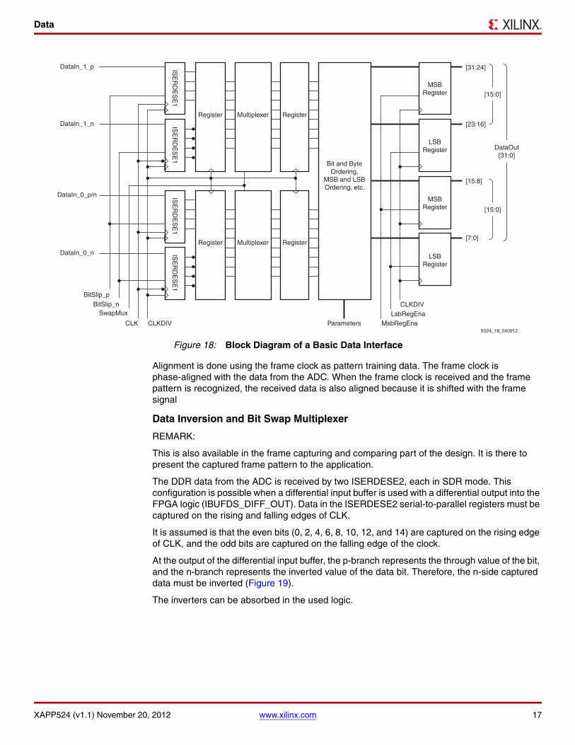
The data output of a basic interface follows the 1-wire or 2-wire selection. In 1-wire mode, the 32-bit output bus is split into two 16-bit output buses. The lower 16 bits are Channel 0, and the upper 16 bits are Channel 1. In 2-wire mode, the 32-bit output represents the same data in the upper and lower 16-bit segments. In the reference design, the upper 16 bits (MSBs) are used (Figure 18).
X-Ref Target - Figure 17
Figure 17: Double Nibble Register BankX524_17_032612
addr
IntRegOutOne
IntRegOutOne
DataIn
IntAddr[4:0]
IntAddr[4:0]IntEqu
IntSrlOutDataIn
FrmClkDiv
IntRstln_d
DataOut
SRLC32E
Register
COMPAREState
Machine
Register
5
Data
XAPP524 (v1.1) November 20, 2012 www.xilinx.com 17
Alignment is done using the frame clock as pattern training data. The frame clock is phase-aligned with the data from the ADC. When the frame clock is received and the frame pattern is recognized, the received data is also aligned because it is shifted with the frame signal
Data Inversion and Bit Swap Multiplexer
REMARK:
This is also available in the frame capturing and comparing part of the design. It is there to present the captured frame pattern to the application.
The DDR data from the ADC is received by two ISERDESE2, each in SDR mode. This configuration is possible when a differential input buffer is used with a differential output into the FPGA logic (IBUFDS_DIFF_OUT). Data in the ISERDESE2 serial-to-parallel registers must be captured on the rising and falling edges of CLK.
It is assumed is that the even bits (0, 2, 4, 6, 8, 10, 12, and 14) are captured on the rising edge of CLK, and the odd bits are captured on the falling edge of the clock.
At the output of the differential input buffer, the p-branch represents the through value of the bit, and the n-branch represents the inverted value of the data bit. Therefore, the n-side captured data must be inverted (Figure 19).
The inverters can be absorbed in the used logic.
X-Ref Target - Figure 18
Figure 18: Block Diagram of a Basic Data Interface
Bit and ByteOrdering,
MSB and LSBOrdering, etc.
MSBRegister
Register
ISE
RD
ES
E1
ISE
RD
ES
E1
ISE
RD
ES
E1
ISE
RD
ES
E1
Register Multiplexer
RegisterRegister Multiplexer
DataIn_1_p
DataIn_1_n
DataIn_0_n
DataIn_0_p/n
X524_18_040912
LSBRegister
MSBRegister
LSBRegister
CLKDIVLsbRegEna
MsbRegEnaCLKDIVCLK
SwapMuxBitSlip_n
BitSlip_p
Parameters
[31:24]
[15:0]
[15:0]
DataOut[31:0]
[23:16]
[15:8]
[7:0]

Data
XAPP524 (v1.1) November 20, 2012 www.xilinx.com 18
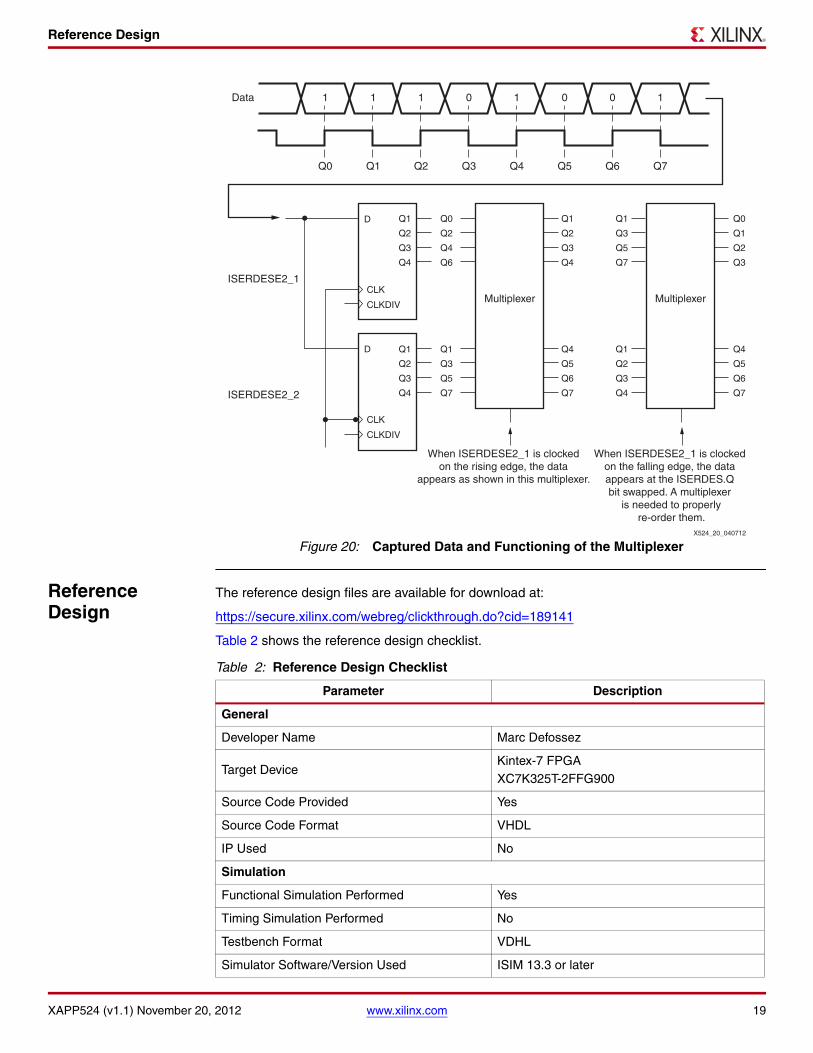
Because it cannot be guaranteed, it is assumed that the even bits are captured on the rising clock edge and the odd bits are captured on the falling clock edge. The even bits could be clocked into the p-side ISERDESE2 on the falling clock edge and the odd bits could be captured on the rising clock edge. Figure 20 illustrates this scenario and shows how the multiplexer reorders the bits.
The edge detection register of the bit clock alignment state machine controls the selection input of the multiplexer.
X-Ref Target - Figure 19
Figure 19: Inverters at the ISERDESE2 OutputX524_19_040612
I
Data 1 1 1 0 1 0 0 1
1 1 1 0 1 0 0 1
0 0 0 1 0 1 1 0
Q0 Q1 Q2 Q3 Q4 Q5 Q6 Q7
IBUFDS_DIFF_OUT
IB
O
OB
CLK
O
OB
O = Incoming Data
The dotted bits must be inverted to get 11101001
OB = Inverse of the Incoming Data
Reference Design
XAPP524 (v1.1) November 20, 2012 www.xilinx.com 19
Reference Design
The reference design files are available for download at:
https://secure.xilinx.com/webreg/clickthrough.do?cid=189141
Table 2 shows the reference design checklist.
X-Ref Target - Figure 20
Figure 20: Captured Data and Functioning of the MultiplexerX524_20_040712
Data
ISERDESE2_1CLK
CLKDIV
Q1
Q2
Q3
Q4
Q1
Q2
Q3
Q4
Q0
Q2
Q4
Q6
Q1
Q3
Q5
Q7
Q1
Q2
Q3
Q4
Q4
Q5
Q6
Q7
Q1
Q3
Q5
Q7
Q1
Q2
Q3
Q4
Q0
Q1
Q2
Q3
Q4
Q5
Q6
Q7
CLK
D
D
CLKDIV
ISERDESE2_2
1 1 1 0 1 0 0 1
Q0 Q1 Q2 Q3 Q4 Q5 Q6 Q7
Multiplexer
When ISERDESE2_1 is clockedon the rising edge, the data
appears as shown in this multiplexer.
When ISERDESE2_1 is clocked on the falling edge, the data appears at the ISERDES.Q bit swapped. A multiplexer
is needed to properlyre-order them.
Multiplexer
Table 2: Reference Design Checklist
Parameter Description
General
Developer Name Marc Defossez
Target DeviceKintex-7 FPGAXC7K325T-2FFG900
Source Code Provided Yes
Source Code Format VHDL
IP Used No
Simulation
Functional Simulation Performed Yes
Timing Simulation Performed No
Testbench Format VDHL
Simulator Software/Version Used ISIM 13.3 or later
Reference Design
XAPP524 (v1.1) November 20, 2012 www.xilinx.com 20
SPICE/IBIS Simulations No
Implementation
Synthesis Tool/Version XST 13.3 or later
Implementation Tool/Version ISE® Design Suite 13.3 or later
Static Timing Analysis Performed Yes
Hardware Verification
Hardware Verified Yes
Hardware Platform Used For Verification KC705 board
Table 3: Device Utilization
Parameters Specification/Details
Maximum Frequency (by speed grade)Kintex-7 FPGA
-1 600 MHz
-2 700 MHz
-3 700 MHz
Device Utilization without Testbench (mandatory) 2%
Device Utilization with Testbench (optional) N/A
QDR II SRAM Operation None
Bus Width None
I/O Standard HP Banks: LVDSHR Banks: LVDS_25
HDL Language Support VHDL
Target Memory Device for Verification None
Table 4: Reference Design Utilization
Slice Logic Utilization Used Available Utilization(%)
Number of Flip-Flops 302 407,600 1%
Number of Occupied Slices 132 50,950 1%
Number Used as Logic 168 356,160 1%
Number Used as Memory 64 64,000 1%
Number Used as Shift Register 0
Number Used Exclusively as Route-Throughs 36
Number of BUFG/BUFGCTRLs 0
Number of ISERDESE2s 12 500 1%
Number of OSERDESE2s 12 500 1%
Number of IODELAYE2s 1 720 1%
Table 2: Reference Design Checklist (Cont’d)
Parameter Description
Revision History
XAPP524 (v1.1) November 20, 2012 www.xilinx.com 21
Revision History
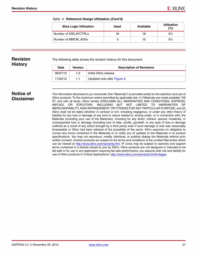
The following table shows the revision history for this document.
Notice of Disclaimer
The information disclosed to you hereunder (the “Materials”) is provided solely for the selection and use ofXilinx products. To the maximum extent permitted by applicable law: (1) Materials are made available "ASIS" and with all faults, Xilinx hereby DISCLAIMS ALL WARRANTIES AND CONDITIONS, EXPRESS,IMPLIED, OR STATUTORY, INCLUDING BUT NOT LIMITED TO WARRANTIES OFMERCHANTABILITY, NON-INFRINGEMENT, OR FITNESS FOR ANY PARTICULAR PURPOSE; and (2)Xilinx shall not be liable (whether in contract or tort, including negligence, or under any other theory ofliability) for any loss or damage of any kind or nature related to, arising under, or in connection with, theMaterials (including your use of the Materials), including for any direct, indirect, special, incidental, orconsequential loss or damage (including loss of data, profits, goodwill, or any type of loss or damagesuffered as a result of any action brought by a third party) even if such damage or loss was reasonablyforeseeable or Xilinx had been advised of the possibility of the same. Xilinx assumes no obligation tocorrect any errors contained in the Materials or to notify you of updates to the Materials or to productspecifications. You may not reproduce, modify, distribute, or publicly display the Materials without priorwritten consent. Certain products are subject to the terms and conditions of the Limited Warranties whichcan be viewed at http://www.xilinx.com/warranty.htm; IP cores may be subject to warranty and supportterms contained in a license issued to you by Xilinx. Xilinx products are not designed or intended to befail-safe or for use in any application requiring fail-safe performance; you assume sole risk and liability foruse of Xilinx products in Critical Applications: http://www.xilinx.com/warranty.htm#critapps.
Number of IDELAYCTRLs 18 18 5%
Number of MMCM_ADVs 0 10 0%
Table 4: Reference Design Utilization (Cont’d)
Slice Logic Utilization Used Available Utilization(%)
Date Version Description of Revisions
08/07/12 1.0 Initial Xilinx release.
11/20/12 1.1 Updated note after Figure 5.