Sequential Networks Two major classes of Sequential Circuits 1.Fundamental Mode – A sequential...
19
Sequential Networks Two major classes of Sequential Circuits 1. Fundamental Mode – A sequential circuit where: • Only one input is allowed to change at any given time • no input change is permitted until internal changes caused by previous input transition have completed. (stable input transition property) Example: latches and flip-flops 2. Pulse Mode – A sequential circuit that responds only to pulses Example: clocked synchronous systems
-
Upload
belinda-short -
Category
Documents
-
view
219 -
download
0
Transcript of Sequential Networks Two major classes of Sequential Circuits 1.Fundamental Mode – A sequential...

Sequential Networks
Two major classes of Sequential Circuits1. Fundamental Mode – A sequential circuit where:
• Only one input is allowed to change at any given time• no input change is permitted until internal changes
caused by previous input transition have completed. (stable input transition property)
Example: latches and flip-flops
2. Pulse Mode – A sequential circuit that responds only to pulses Example: clocked synchronous systems

Model of Sequential Networks
CombinationalLogicCircuit
Memory Elements - flip-flop - latch - register - PROM
n m
s s
s-bitPresent StateVariables, Y
s-bit Next State Excitation Variables Ei (X,Y)
Input Variables, X Output Variable, Z
yi (t+ti)
xi (t)
yi (t)

Sequential Logic Model
• Composed of Combinational Logic and Memory Elements
• Behavior is Given by Logic values at Discrete
Time Instances
• Discrete Time Instances are Given by Clock Signal
• Memory Elements
– Edge-Triggered Flip-Flops
– Level-Sensitive Latches
• Memory Elements Can Only Load at Discrete
Time Instance
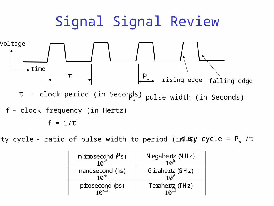
Signal Signal Review
time
voltage
f = 1/
Pw rising edge falling edge
- clock period (in Seconds) Pw - pulse width (in Seconds)
f – clock frequency (in Hertz)
duty cycle - ratio of pulse width to period (in %) duty cycle = Pw /
microsecond (s) 10-6
Megahertz (MHz) 106
nanosecond (ns) 10-9
Gigahertz (GHz) 109
picosecond (ps) 10-12
Terahertz (THz) 1012

Clock Signal Example
What is the pulse-width of a 4.77 MHz clock with a 30% duty cycle?
= 1/f = (4.77×10⁶)-1 = 2.096 ×10-7 = 210 ns
Pw = (duty cycle) × = (0.3) × (210 ns) = 63 ns
What about clock rise- and fall-time? Clocks are normally defined as having maximum rise and fall times (e.g., time between 10% and 90% values) or they are implied through pulse width specifications.

Common Memory Element - Flip-Flops
S
R
Q
Q
Q
Q
J
K
Q
Q
D Q
Q
T
Behavior is Described by Characteristic Table or Equation
Most Commonly Encountered Device is the D-flip-flop
S R Q(t+1)0 0 Q(t)0 1 01 0 11 1 undef
J K Q(t+1) 0 0 Q(t) 0 1 0 1 0 1 1 1 Q'(t)
D Q(t+1)0 01 1
T Q(t+1) 0 Q(t) 1 Q'(t)
( 1) ( )Q t S RQ t ( 1) ( ) ( )Q t JQ t KQ t ( 1)Q t D ( 1) ( ) ( )Q t TQ t TQ t

Concept of State
• The Q Outputs of the Flip-Flops Form a State Vector
• A Particular Set of Outputs is the Present State
• The Particular State Vector that will Occur at the Next
Discrete Time is the Next State
• A Sequential Circuit described in Terms of State is a
Finite State Machine (FSM)

FSM Analysis Example
x
CLK
A
B
y
( 1) ( ) ( ) ( ) ( )
( 1) ( ) ( )
( ) [ ( ) ( )] ( )
A t A t x t B t x t
B t A t x t
y t A t B t x t
State Equations:
Preset State: A (t)B (t)
Next State: A(t+1)B(t+1)

Representing/Describing FSMsPresent State Next State Output
x=0 x=1 x=0 x=1 A(t)B(t) A(t+1)B(t+1) A(t+1)B(t+1) y(t) y(t)
00 00 01 0 0 01 00 11 1 0 10 00 10 1 0 11 00 10 1 0
00
01 11
0/0
0/1
1/0
1/0
1/0
0/1
0/11/0
Present State
Output
Input
Transition Table
State Diagram
10
Note a State Table does not necessarily have the state assignment

Representing/Describing FSMsPresent State Next State Output
x=0 x=1 x=0 x=1 A(t)B(t) A(t+1)B(t+1) A(t+1)B(t+1) y(t) y(t)
00 00 01 0 0 01 00 11 1 0 10 00 10 1 0 11 00 10 1 0
State Table
Timing Diagram
CLK
A
B
x
y
Note: propagation delaysand change in y beforeclock edge

FSM Design
• Specification Given as One of Previous Descriptions– State Table– State Equations– State Diagram (Easiest to Generate Initially)– ASM Chart (Preferred)
• Designer’s Job is to Generate Schematic• Instead of Characteristics, we are Given Excitations• Individual flip-flops have Specific Excitations

Flip-Flop Excitations
S
R
Q
Q
Q
Q
J
K
Q
Q
D Q
Q
T
Input Behavior is Described by Excitation Table or Equation
Most Commonly Encountered Device is the D-flip-flop
Q(t) Q(t+1) S R0 0 0 X0 1 1 01 0 0 11 1 X 0
Q(t) Q(t+1) D0 0 00 1 11 0 01 1 1
Q(t) Q(t+1) J K 0 0 0 X 0 1 1 X 1 0 X 1 1 1 X 0
Q(t) Q(t+1) T0 0 00 1 11 0 11 1 0

Alternate Scheme for Mapping Excitation for SR Latch in One Map
Q(t) Q(t+1) S R 0 0 0 r 0 1 S 0 1 0 0 R 1 1 s 0
• S, R, s, and r cannot be 1 at the same time, one map can be used for generating Set and Reset equations
• For Set must encircle S and s is don’t care• For Reset must encircle R and r is don’t care

Vending Machine Example(US version)
• Soft drink sells for $.75• Machine accepts quarter and half-dollar coins
• Input x1 =1 if machine receives a half-dollar
• Input x2 = 1 if machine receives a quarter
• Output z1 = 1 if machine is to give drink
• Output z2 = 1 if machine is to give change

Vending Machine ExampleState Diagram and State Table
Q0, initial state without money
Q2, machine received a half-dollar
Q1, machine received a quarter

Vending Machine ExampleState Assignment and Transition Table

Vending Machine ExampleSR Implementation with Separate Maps

Vending Machine ExampleSR Implementation with Single Maps
r
00 01 11 10
00
01
11
10
y1 y2
x1 x2
s
r
r
r
S
dd
d
d
d
d
d
S
R R
y1
r
00 01 11 10
00
01
11
10
y1 y2
x1 x2
r
s
S
R
r
dd
d
d
d
d
d
R
r r
y2

Vending Machine ExampleOutputs
00 01 11 10
00
01
11
10
y1 y2
x1 x2
1
dd
d
d
d
d
d1 1
z1
00 01 11 10
00
01
11
10
y1 y2
x1 x2
dd
d
d
d
d
d 1
z2