Sequential Circuits
52
Sequential Circuits
-
Upload
ryan-mcdaniel -
Category
Documents
-
view
18 -
download
1
description
Sequential Circuits. Sequential vs. Combinational. Combinational Logic: Output depends only on current input TV channel selector (0-9) Sequential Logic: Output depends not only on current input but also on current state of the system (which depends on past input values) - PowerPoint PPT Presentation
Transcript of Sequential Circuits
Sequential Circuits

2
Sequential vs. Combinational
• Combinational Logic: Output depends only on current input
− TV channel selector (0-9)
• Sequential Logic: Output depends not only on current input but also on current
state of the system (which depends on past input values)− TV channel selector (up-down)
Need some type of memory to remember the current state
inputs outputssystem
3
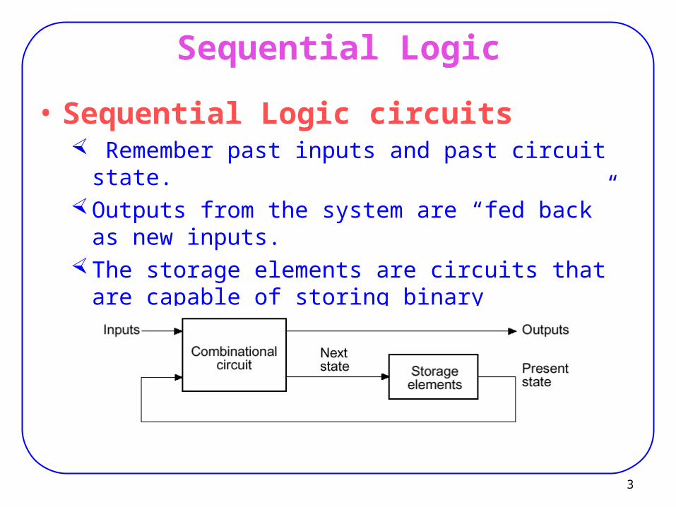
Sequential Logic
• Sequential Logic circuits Remember past inputs and past circuit state.Outputs from the system are “fed back” as new inputs.The storage elements are circuits that are capable of
storing binary information: memory.

4
Feedback Loop• Feedback:
A signal s1 depends on another signal whose value depends on s1 − (perhaps with several intermediate signals).
s1

5
Base of MemoryConsider the following circuit:
It can differentiate between two different states as it has only one feedback line that can keep one of two values, 0 or 1.
A circuit with n feedback lines has 2n potential states, and that the memory of our circuit depends on the number of its feedback lines:
PI
PI
01
n
6
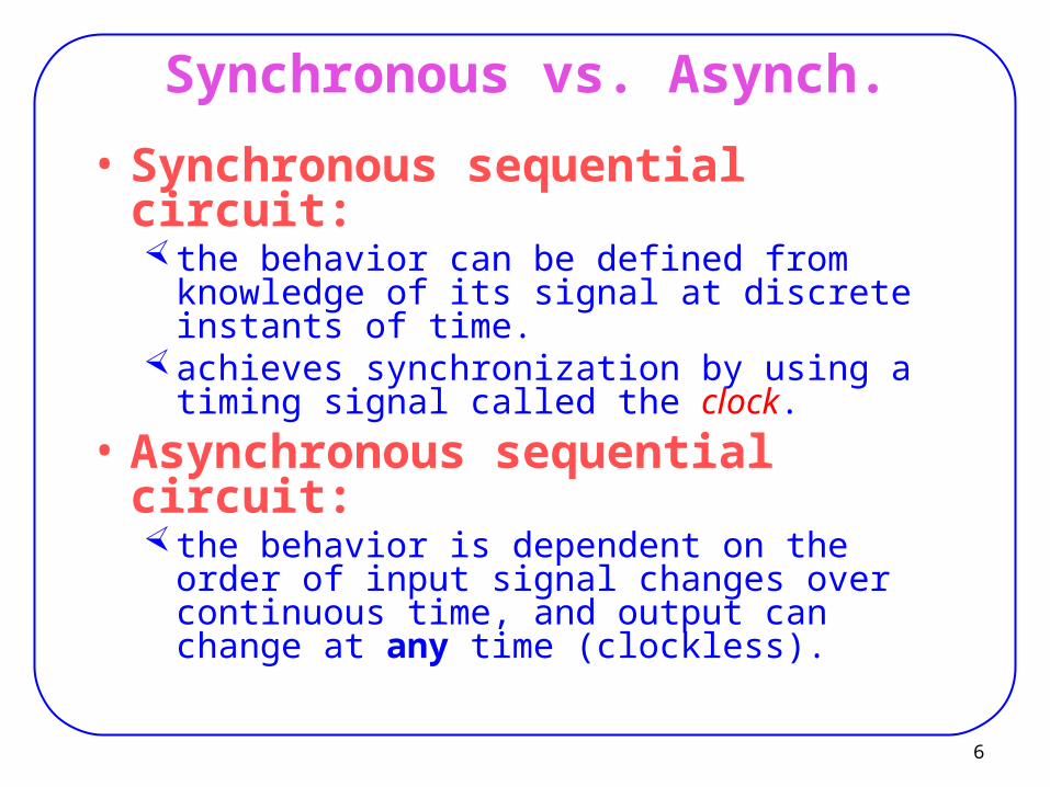
Synchronous vs. Asynch.
• Synchronous sequential circuit: the behavior can be defined from knowledge of its
signal at discrete instants of time. achieves synchronization by using a timing signal
called the clock.
• Asynchronous sequential circuit: the behavior is dependent on the order of input
signal changes over continuous time, and output can change at any time (clockless).

7
Clock Signal
Different duty cycles
Clock generator: Periodic train of clock pulses
Rising Clock Edge
Falling Clock Edge
8
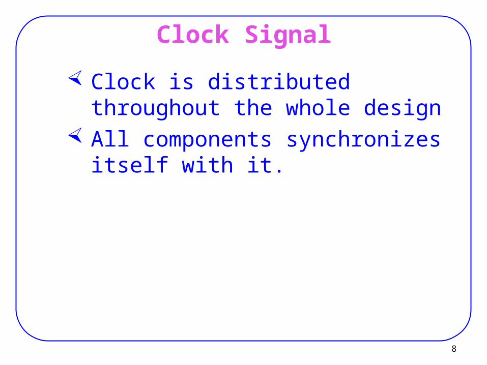
Clock Signal
Clock is distributed throughout the whole design
All components synchronizes itself with it.

9
Synchronous Circuits
Combinational
Logic
time
clk

10
SR latch (NOR version)
RS
R
S
Q
Q’
Q
hold 0 1
unstable
S
0 0 1 1
R
0 1 0 1
Truth Table:Next State = F(S, R, Current State)
S(t) R(t) Q(t) Q(t+)
0 0 0 0 (hold)0 0 1 1 (Hold)0 1 0 0 (reset)0 1 1 0 (reset)1 0 0 1 (set)1 0 1 1 (set)1 1 0 Not allowed1 1 1 Not allowed

11
SR LatchTruth Table:Next State = F(S, R, Current State)
S
R
Q
R-SLatch Q+
Derived K-Map:
Characteristic Equation:
Q+ = S + R Q t
R
SR 00 01 11 10
0 0 X 1
1 0 X 1
0
1
Q ( t )
S
S(t) R(t) Q(t) Q(t+)
0 0 0 0 (hold)0 0 1 1 (Hold)0 1 0 0 (reset)0 1 1 0 (reset)1 0 0 1 (set)1 0 1 1 (set)1 1 0 Not allowed1 1 1 Not allowed
12
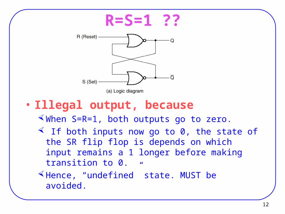
R=S=1 ??
• Illegal output, becauseWhen S=R=1, both outputs go to zero. If both inputs now go to 0, the state of the SR flip
flop is depends on which input remains a 1 longer before making transition to 0.
Hence, “undefined” state. MUST be avoided.
13
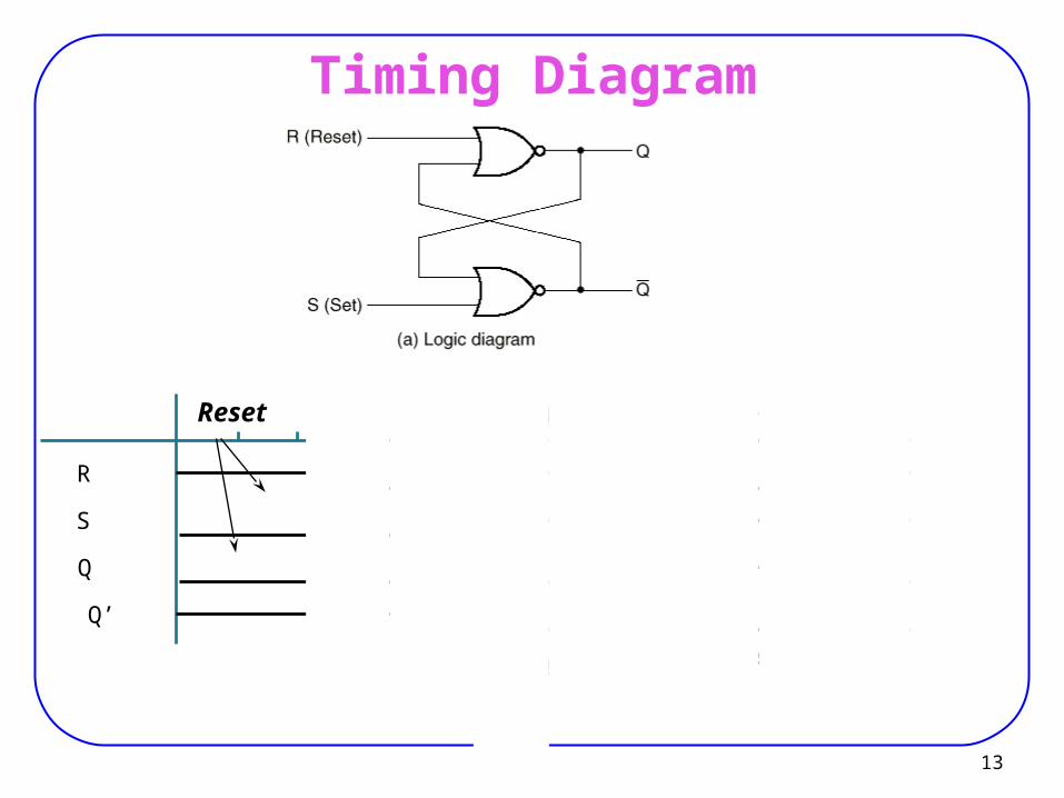
Timing Diagram
100
R
S
Q
Q’
Reset Hold Set
ForbiddenState
Reset Set
ForbiddenState
Race
14
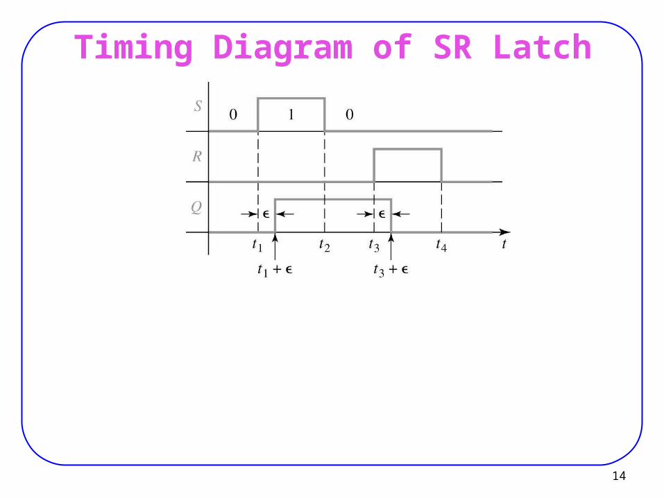
Timing Diagram of SR Latch
15
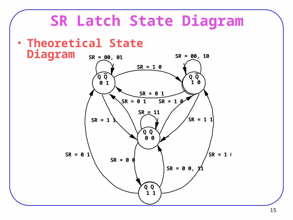
SR Latch State Diagram
• Theoretical State Diagram
Q Q Q Q
Q Q
0 1 1 0
0 0
SR = 1 0
SR = 0 1
SR = 0 1
SR = 1 1
SR = 1 0
SR = 1 1
SR = 00, 01 SR = 00, 10
Q Q1 1
SR = 0 0
SR = 0 0, 11
SR = 11
SR = 1 0SR = 0 1
Q Q Q Q
Q Q
0 1 1 0
0 0
Q Q1 1

16
SR Latch State Diagram
Very difficult to observe R-S Latch in the 1-1 state Ambiguously returns to state 0-1 or 1-0
Q Q Q Q
Q Q
0 1 1 0
0 0
Q Q Q Q
Q Q
0 1 1 0
0 0
SR = 1 0
SR = 0 1
SR = 0 1
SR = 1 1
SR = 1 0
SR = 1 1
SR = 00, 01 SR = 00, 10
SR = 0 0
SR = 11
SR = 0 0
• Observed State Diagram

17
S’R’ Latch (NAND version)
S’
R’
Q
Q’
0 00 11 01 1
S’ R’ Q Q’0
1
1
0
1 0 Set
0 0 1 0 1 1 1 0 1 1 1 0
X Y NANDS
R
R-SLatch
Q
Q’
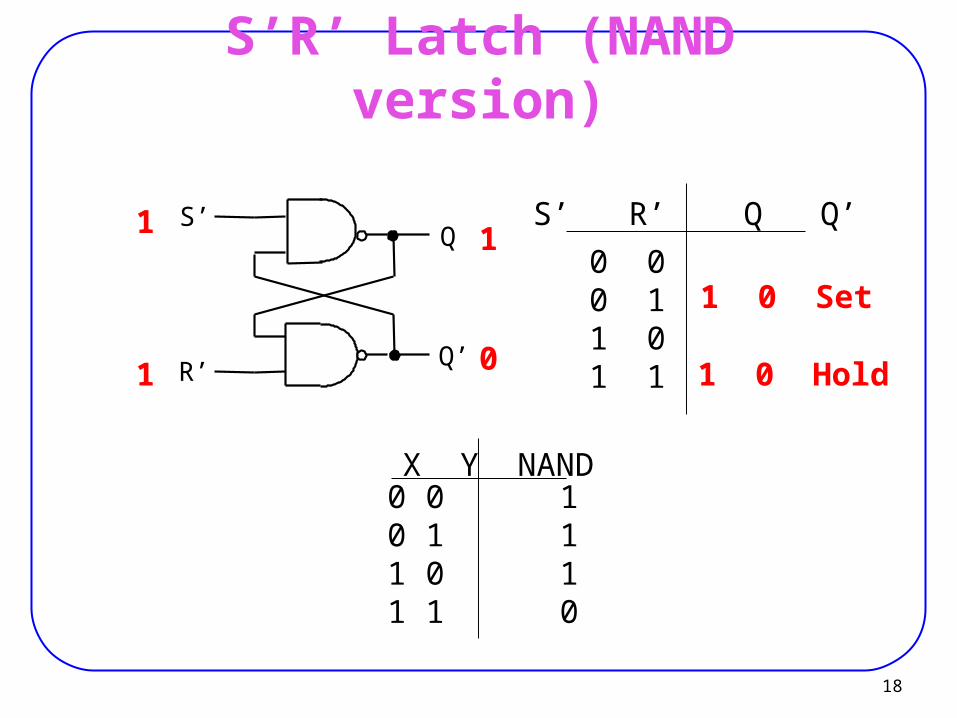
18
S’R’ Latch (NAND version)
S’
R’
Q
Q’
0 00 11 01 1
S’ R’ Q Q’1
1
1
0 1 0 Hold
0 0 1 0 1 1 1 0 1 1 1 0
X Y NAND
1 0 Set

19
S’R’ Latch (NAND version)
S’
R’
Q
Q’
0 00 11 01 1
S’ R’ Q Q’1
0
0
1
0 0 1 0 1 1 1 0 1 1 1 0
X Y NAND
1 0 Hold
1 0 Set0 1 Reset

20
S’R’ Latch (NAND version)
S’
R’
Q
Q’
0 00 11 01 1
S’ R’ Q Q’1
1
0
1
0 0 1 0 1 1 1 0 1 1 1 0
X Y NAND
0 1 Hold
1 0 Set0 1 Reset1 0 Hold

21
S’R’ Latch (NAND version)
S’
R’
Q
Q’
0 00 11 01 1
S’ R’ Q Q’0
0
1
1
0 0 1 0 1 1 1 0 1 1 1 0
X Y NAND
0 1 Hold
1 0 Set0 1 Reset1 0 Hold
1 1 Disallowed
22
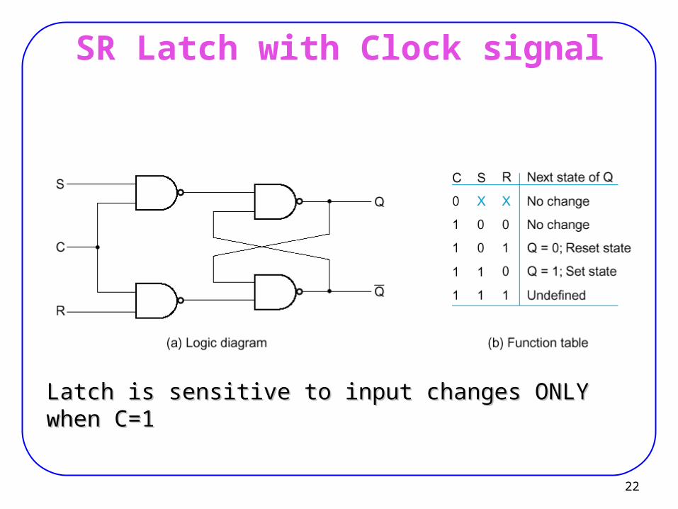
SR Latch with Clock signal
Latch is sensitive to input changes ONLY when C=1Latch is sensitive to input changes ONLY when C=1

23
SR Latch with Clock signal
S’
R’
Q
Q’
S
R
CLK
S R CLK S’ R’ Q Q’
0 0 1 1 1 Q0 Q0’ Store 0 1 1 1 0 0 1 Reset1 0 1 0 1 1 0 Set1 1 1 0 0 1 1 DisallowedX X 0 1 1 Q0 Q0’ Store
24
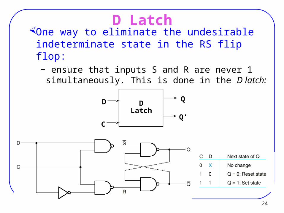
D LatchOne way to eliminate the undesirable
indeterminate state in the RS flip flop:− ensure that inputs S and R are never 1
simultaneously. This is done in the D latch:
D
C
DLatch
Q
Q’
25
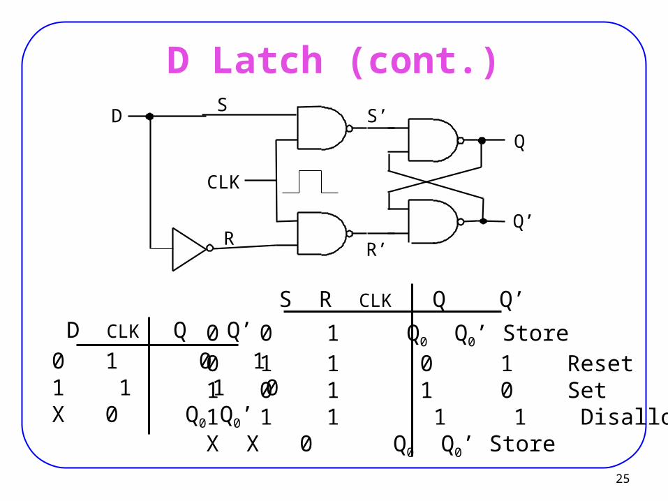
D Latch (cont.)D
S R CLK Q Q’
0 0 1 Q0 Q0’ Store 0 1 1 0 1 Reset1 0 1 1 0 Set1 1 1 1 1 DisallowedX X 0 Q0 Q0’ Store
0 1 0 11 1 1 0X 0 Q0 Q0’
D CLK Q Q’
S’
R’
Q
Q’
S
R
CLK
26
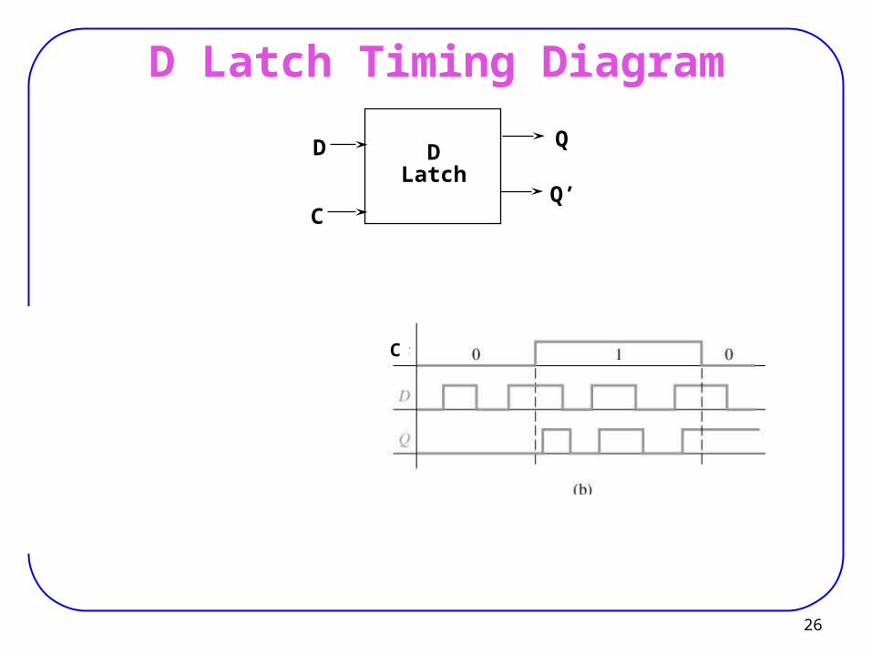
D Latch Timing Diagram
D
C
DLatch
Q
Q’
C

27
D-Latch Circuit
G D Q Q+
0 0 00 0 10 1 00 1 11 0 01 0 11 1 01 1 1
01010011
28
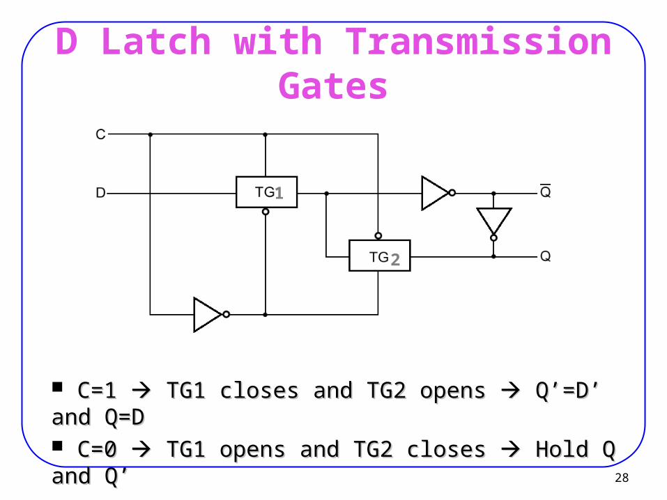
D Latch with Transmission Gates
C=1 C=1 TG1 closes and TG2 opens TG1 closes and TG2 opens Q’=D’ and Q’=D’ and Q=DQ=D C=0 C=0 TG1 opens and TG2 closes TG1 opens and TG2 closes Hold Q and Hold Q and Q’Q’
2
1

29
JK Latch
J, K both one yields toggle
Characteristic Equation:
Q+ = Q K’ + Q’ J
K
J Q
Q’
J-K Latch
J(t) K(t) Q(t) Q(t+)
0 0 0 0 (hold)0 0 1 1 (Hold)0 1 0 0 (reset)0 1 1 0 (reset)1 0 0 1 (set)1 0 1 1 (set)1 1 0 1 (toggle)1 1 1 0 (toggle)
Derived K-Map:
K
JK 00 01 11 10
0 0 1 1
1 0 0 1
0
1
Q ( t )
J

30
JK Latch Using SR LatchHow to eliminate the forbidden state in SR?
Idea: use output feedback to guarantee that R and S are never both one
J, K both one yields toggle
Characteristic Equation:
Q+ = Q K + Q J
J(t) K(t) Q(t) Q(t+)
00
00
01
0 HOLD
1
00
11
01
0 RESET
0
11
00
01
1 SET
1
11
11
01
1 TOGGLE
0
R-S latch
K
J S
R
Q
Q’ Q’
Q

31
JK Lacth Race Condition
J
K
Q
\ Q
100 Set Reset Toggle
Toggle Correctness: Single State change per clocking event
Solution: Master/Slave Flipflop

32
Flip-Flops
Latches are “transparent” (= any change on the inputs is seen at the outputs immediately).
This causes synchronization problems!
Solution: use latches to create flip-flops that can respond (update) ONLY on SPECIFIC times (instead of ANY time).
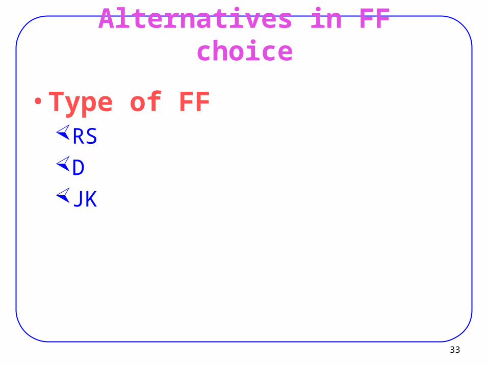
33
Alternatives in FF choice
• Type of FFRSDJK

34
D-FF
0 00 11 01 1
0011
D Q Q
c Truth table
DQ
Timing for D Flip-Flop (Falling-Edge Trigger)

35
Rising Edge D-FF
Falling-Edge Circuit?

36
Symbols
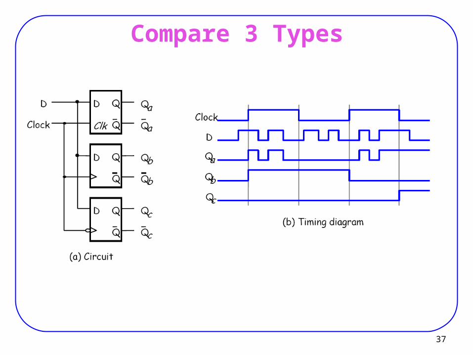
37
Compare 3 Types

38
Setup & Hold Times
Setup and Hold Times for an Edge-Triggered D Flip-Flop

39
Edge-Triggered D Flip-Flop
Figure 11-17. Determination of Minimum Clock Period

40
Master-Slave FF configuration using SR latches
– Enables level-triggered behaviorEnables level-triggered behavior

41
S R CLK Q Q’
0 0 1 Q0 Q0’ Store 0 1 1 0 1 Reset1 0 1 1 0 Set1 1 1 1 1 DisallowedX X 0 Q0 Q0’ Store
Master-Slave FF configuration using SR latches (cont.)
•When C=1, master is enabled and stores new data, slave stores old data.•When C=0, master’s state passes to enabled slave (Q=Y), master not sensitive to new data (disabled).
Master Slave
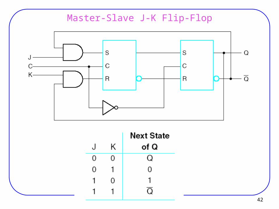
42
Master-Slave J-K Flip-Flop

43
Master-Slave J-K Flip-Flop
Sample inputs while clock high Sample inputs while clock low
Uses time to break feedback path from outputs to inputs!Uses time to break feedback path from outputs to inputs!
Correct ToggleOperation
P
P’
Master outputs
Slave outputs
Set Reset T oggle 1's
Catch 100
J
K
C
P
P‘‘
Q
Q’
44
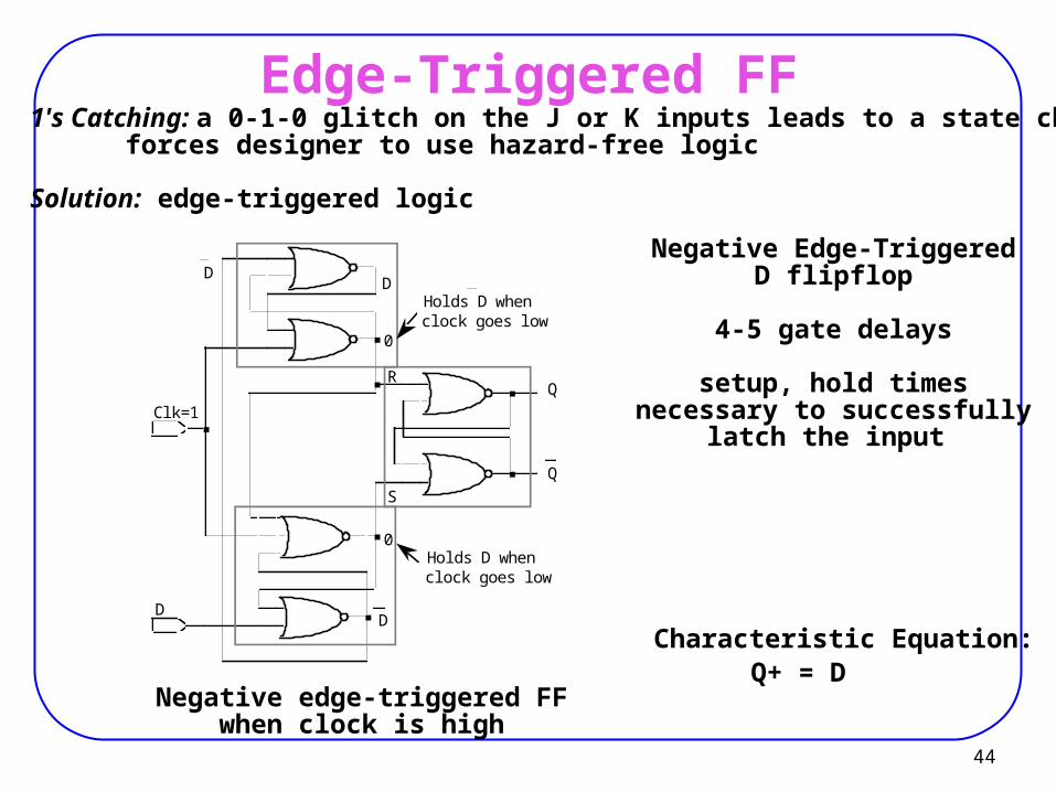
Edge-Triggered FF1's Catching: a 0-1-0 glitch on the J or K inputs leads to a state change! forces designer to use hazard-free logic
Solution: edge-triggered logic
Negative Edge-TriggeredD flipflop
4-5 gate delays
setup, hold timesnecessary to successfully
latch the input
Characteristic Equation:Q+ = D
Q
Q
D
Clk=1
R
S
0
0
D
DD
Holds D when clock goes low
Holds D when clock goes low
Negative edge-triggered FFwhen clock is high

45
T Flip-Flop
T Flip-Flop
0 00 11 01 1
0110
T Q Q
b
QTQTQTQ
Timing Diagram for T Flip-Flop (Falling-Edge Trigger)
46
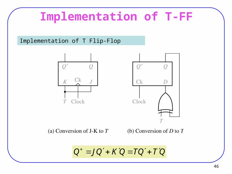
Implementation of T-FF
Implementation of T Flip-Flop
QTQTQKQJQ
47
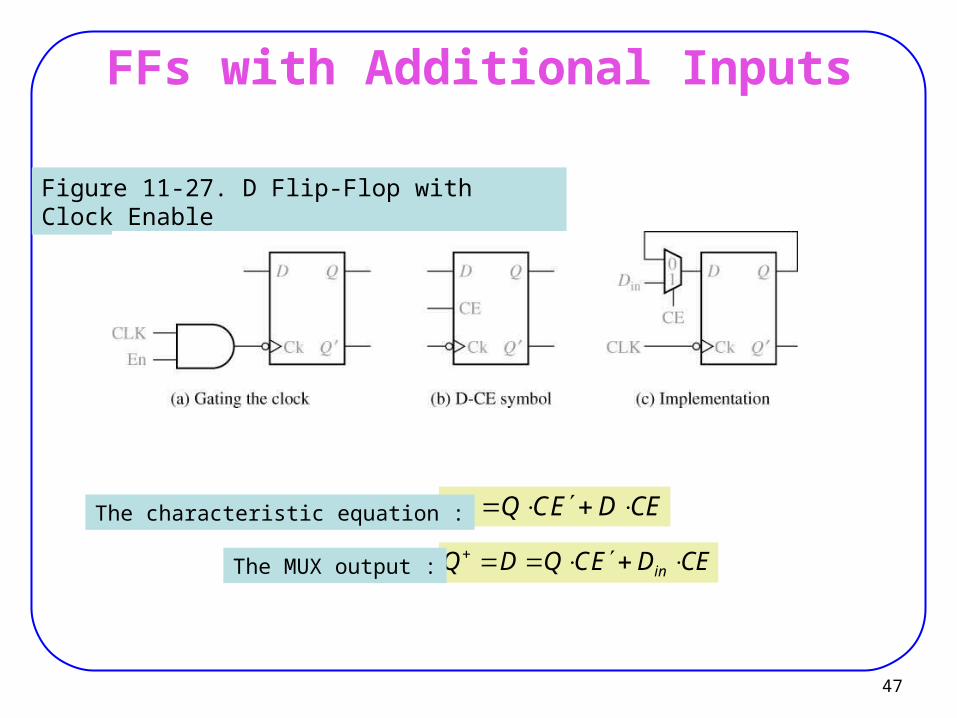
FFs with Additional Inputs
Figure 11-27. D Flip-Flop with Clock Enable
CEDECQQ
CEDECQDQ in The MUX output :
The characteristic equation :
48
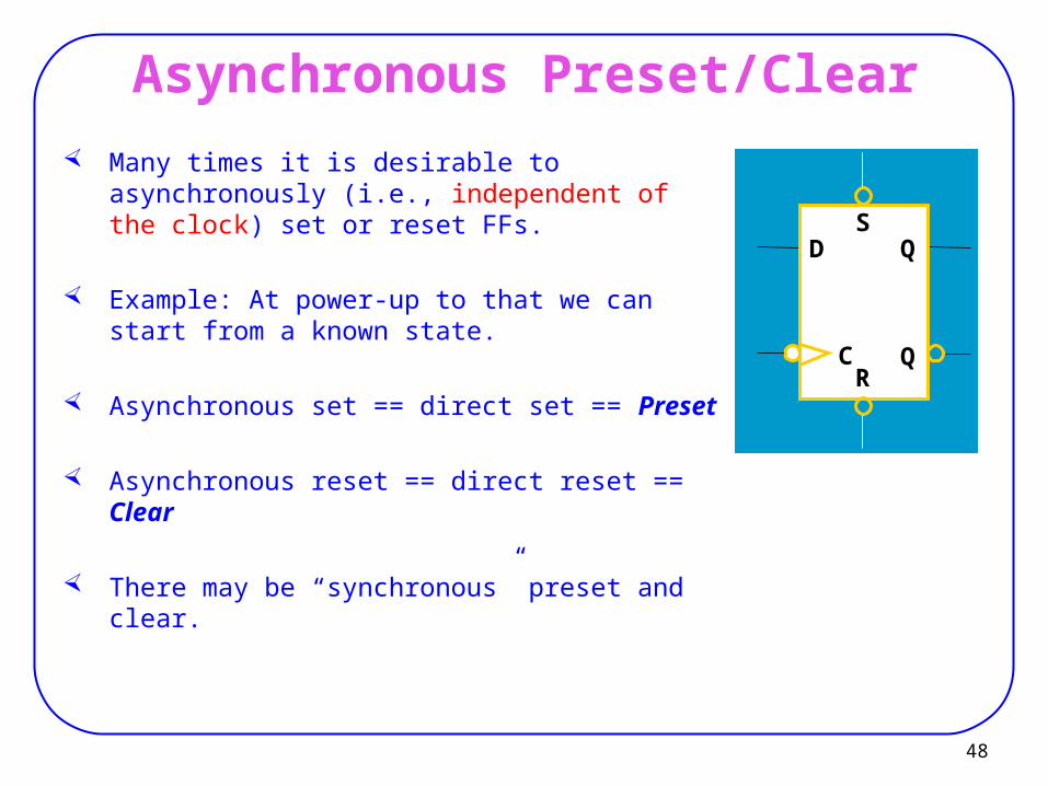
Asynchronous Preset/Clear
Many times it is desirable to asynchronously (i.e., independent of the clock) set or reset FFs.
Example: At power-up to that we can start from a known state.
Asynchronous set == direct set == Preset
Asynchronous reset == direct reset == Clear
There may be “synchronous” preset and clear.
D
C
S
R
Q
Q

49
Asynchronous Set/Reset
S
C1
1J
1K
R
IEEE standard graphics symbol for JK-FF with direct set & reset
Cn indicates that Cn controls all other inputs whose label starts with n. In this case, C1 controls J1 and K1.
S R C1 1J 1K Q(t+1)
0 1 X X X 1 – Preset
1 0 X X X 0 – Clear
0 0 X X X Undefined
1 1 0 0 Q(t) – Hold
1 1 0 1 0 – Reset
1 1 1 0 1 – Set
1 1 1 1 Q(t)’ -- Complement
Function Table
50
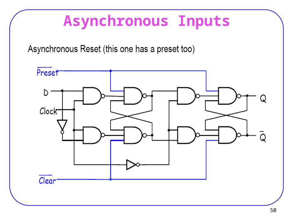
Asynchronous Inputs

51
Synchronous Reset

52
Timing Parameters
• ts - setup time• th - hold time• tw - clock
pulse width• tpx - propa-
gation delay tPHL - High-to-
Low tPLH - Low-to-
High tpd - max (tPHL,
tPLH)