Sept 2011LCWS 2011 - CLIC DB Klystron Modulators1 1 CLIC Drive Beam Klystron Modulators R&D status &...
20
Sept 2011 LCWS 2011 - CLIC DB Klystron Modulators 1 CLIC Drive Beam Klystron Modulators R&D status & prospects David Nisbet, Davide Aguglia, Eleni Sklavounou, Serge Pittet TE EPC
-
Upload
dustin-elliott -
Category
Documents
-
view
216 -
download
0
Transcript of Sept 2011LCWS 2011 - CLIC DB Klystron Modulators1 1 CLIC Drive Beam Klystron Modulators R&D status &...
Sept 2011 LCWS 2011 - CLIC DB Klystron Modulators 11
CLIC Drive Beam Klystron Modulators
R&D status & prospectsDavid Nisbet, Davide Aguglia, Eleni Sklavounou,
Serge Pittet
TE EPC

Objectives
Sept 2011 LCWS 2011 - CLIC DB Klystron Modulators 2
Peak power/klystron 15 MW
Train length after injection 140 ms
Repetition rate 50 Hz
Klystrons efficiency 65% (70% target)
Overall modulator efficiency 89%
Phase precision
0.05° @ 1 GHz (first 10% of the DB linac)0.2° @ 1 GHz (next 90% of the DB linac)
Nb of klystrons (DB linac) 2x 797 = 1594
Everything (for the modulator) starts here…

Modulator Efficiency
Sept 2011 LCWS 2011 - CLIC DB Klystron Modulators 3
Useful flat-top Energy 22MW*140μs = 3.08kJ
Rise/fall time energy 22MW*5μs*2/3= 0.07kJ
Set-up time energy 22MW*5μs = 0.09kJ
Pulse efficiency 0.95
Pulse forming system efficiency
0.98
Charger efficiency 0.96
Power efficiency 0.94
Overall Modulator efficiency
89%

Pulse requirements
Sept 2011 LCWS 2011 - CLIC DB Klystron Modulators 4
•Rise time: needed to reach the requested voltage.•Settling time: needed to damp oscillations within the droop window.•Droop: window in which remaining reproducible oscillations can be cancelled by RF feed-forward.•Reproducibility: maximum difference allowed between two consecutive pulses.•Fall time: time for voltage to return to zero.
20ms
Flat topFall time (losses)
Rise time (losses)
Reproducibility
Settling time
Droop
Beam

5
Converters reproducibility
10^-5 Reproducibility not even close to the some ever reached on pulse applications
Not a common topic, no defined theory on the issue so far We propose new theory
What is the influence of the switches jitter? What is a typical jitter of an IGBT? We are trying to answer these questions….
Some numbers (example):
• Buck; Vin=3000 V; D=50%; Vout=1500V; Stab Spec=10^-3 1.5VL=25mH; f=25kHz; C=4uF; DVR Spec=10^-5 15mV Maximal jitter 50ns• Semikron 1203GB172-2DW (IGBT with Driver) jitter = 150ns Expected 47mV of DVR
Out of Spec!
Pulse-to-pulse reproducibility of a switching power converter mainly depends on : switches jitter, switching frequency, measurement reproducibility.
Sept 2011 LCWS 2011 - CLIC DB Klystron Modulators

6
Method Status:Validated (analytical vs. numerical methods)
Active Part model (frequency)
PassivePart model (frequency)
For each harmonic Reproducibility can be define as:
Some trigonometry
Algorithm:
Example: Buck converter
Converters reproducibilityStudy approach
A wide variety of IGBTs and drivers have been ordered to measure typical jitters and obtain a technological state of the art on the subject from current industrial solutions
Sept 2011 LCWS 2011 - CLIC DB Klystron Modulators

Pulsed HV measurements
Sept 2011 LCWS 2011 - CLIC DB Klystron Modulators 7
If measurement performance does not exceed the red line, performance cannot be demonstrated
Between the red and green lines, performance can be measured and sorted to meet requirements
If measurement performance exceeds the green line, feedback on the output voltage may be implemented to fulfill the specification (provided that a 300A/5MHz active voltage compensation can be implemented!)
• The use of indirect high bandwidth measurement on RF phase to implement a feedback on the modulator voltage and/or on the klystron RF_input modulation must be studied in parallel.
• Strongly recommend that phase reproducibility must not rely ONLY on modulator performance

Power from network
Sept 2011 LCWS 2011 - CLIC DB Klystron Modulators 8
•Modulator charging is usually stopped before the output pulse generation. Induces large power transients on the 400kV network and can affect grid stability and quality.
•Studies of methods to assure a constant power load to the grid have begun.
•Other issues will also to be considered (eg how to manage modulator power shutdown, finding optimal charger efficiency, etc).
•R&D started in 2011 (1 fellow).
Pulse time200ms
Charging time1800ms
Time
400k
V N
etw
ork
Pow
er
Existingsystems
CLIC goal

POWER FROM NETWORK: R&D OBJECTIVES Propose design solution for the modulators charging
sub-system minimizing the grid power fluctuation.
Design the control strategy of capacitor chargers for minimum power fluctuation.
Problematic: Grid power fluctuation
VS capacitors voltage droop + current and voltage
regulation capabilities of the charger + cost + size
ChargerPulse Forming
System(PFS)
KlystronC
Ich Icdis
Vch
Ik
Vmod
Modulator
PRFPmodulatorPgrid Pcharger
Se
pt 2
011
9
LC
WS
20
11 - C
LIC
DB
Klystro
n M
od
ula
tors

Example:
If we consider a constant charging current:
Charger Power
0 0.01 0.02 0.03 0.04 0.05 0.06 0.070
500
1000
1500
2000
2500
3000
3500
4000
4500
5000
5500Charging voltage
time [sec]
VC
ma
in [
V]
0 0.01 0.02 0.03 0.04 0.05 0.06 0.070
5
10
15
20
25
30
35
40
45
50Constant charching current
time [sec]
I ch [
A]
0 0.01 0.02 0.03 0.04 0.05 0.06 0.070
0.5
1
1.5
2
2.5x 10
5 Charger Power for constant Ich
time [sec]
PC
h [
W]
Ca
paci
tor
Ch
arge
r C
R
SW
Se
pt 2
011
10
LC
WS
20
11 - C
LIC
DB
Klystro
n M
od
ula
torsUnacceptable
power fluctuation!!!

But if we want a constant charger power: (we model the capacitor charger as a 2nd order transfer function)
Power Consumption
0 0.01 0.02 0.03 0.04 0.05 0.06 0.070
500
1000
1500
2000
2500
3000
3500
4000
4500
5000
5500Charging voltage
time [sec]
VC
ma
in [
V]
0 0.01 0.02 0.03 0.04 0.05 0.06 0.070
10
20
30
40
50
60Ideal and Real charging current
time [sec]
I ch [
A]
Ideal currentReal current
0.05 0.051 0.052
42
44
46
48
50
52
0 0.01 0.02 0.03 0.04 0.05 0.06 0.070
0.5
1
1.5
2
2.5x 10
5 Ideal and Real power of the charger
time [sec]
PC
h [
W]
Ideal PCh
Real PCh
0.05 0.0505 0.051
1.8
1.85
1.9
1.95
2
2.05
2.1
x 105
*Ideal case: infinite current bandwidth*Real case: 2kHz current bandwidth
Se
pt 2
011
11
LC
WS
20
11 - C
LIC
DB
Klystro
n M
od
ula
tors
Very high bandwidth
charger needed
At a few ppms!

1ST RESULTS FOR THE GRID ACTIVE POWER
For different Cint and Bandwidth of the charger
0 0.5 1 1.5 2
x 104
0
5
10
15
20
25Grid Active Power Fluctuation [%]
Charger's DC/DC converter bandwidth [Hz]
Pg
rid [
%]
Cint
=800uF; Volume= 1% of a Rack
Cint
=4mF; Volume= 2% of a Rack
Cint
=8mF; Volume= 3.2% of a Rack
Cint
=80mF; Volume= 25% of a Rack
Cint
=800mF; Volume= 2.5 Racks
Se
pt 2
011
12
LC
WS
20
11 - C
LIC
DB
Klystro
n M
od
ula
tors

Current research:Describe the closed loop system as a transfer function and put this transfer function in the simplified transfer function model in order to obtain faster models to simulate several systems in parallel.
What’s next?Power Fluctuation VS Charging Voltage:
How can I slow down/speed up the charging of Cmain in order to reach always the same Vch at the end of each pulse for all the 1638 chargers?
Present Future
Se
pt 2
011
13
LC
WS
20
11 - C
LIC
DB
Klystro
n M
od
ula
tors

14
AC voltage level selection
IGBTs up to 1.7kV (1kV DC-Bus) easily operate at high switching frequencies (20kHz) thus high converter bandwidth (low power fluctuations)
IGBTs higher than 1.7kV are operating at lower switching frequencies 6.5kV IGBTs are for the drive industry, meaning high current…we don’t need
high currents! What is certain: The higher the AC voltage, the more expensive the charger
(compared to a step down transformer) and the lower the bandwidth (leading to more cost on an external active power compensator/storage system).
For high efficiency switching power converters are required.Switches that can be used:IGBTs or IGCTs (6.5kV max)
AC voltage selection has a direct impact on charger topology, cost and performances. A deep study of this subject is required. External collaborations are starting on this subject as well!
Cha
rger
Pul
se F
orm
ing
Sys
tem
(P
FS
)
Modulator
Kly
stro
n
Util
ity g
rid
400/36kV 150kV??kV
Sept 2011 LCWS 2011 - CLIC DB Klystron Modulators

R&D objectives and planning
Sept 2011 LCWS 2011 - CLIC DB Klystron Modulators 15
Tentative Milestones Year
Invite proposals and select partners 2011
From submitted studies, select at least one topology for prototyping 2012
Begin construction of full scale prototypes 2014
Deliver 2 validated full scale modulator prototypes 2016
• Maximise charger efficiency and power quality– Objective: better than 90% efficiency with constant power consumption
• Minimise rise, fall and settling time– Objective for 140us pulse: less than 10us total for rise, fall and setup time
• Maximise operational reliability and availability– Objective: design for 100% availability assuming interventions every 14 days
• Guarantee exceptional pulse-to-pulse voltage reproducibility– Objective: 10-5 (10ppm) from pulsen-1 to pulsen (RF feedforward gives long term performance)
• Optimise volume – Objective: mechanical implementation compatible with one system every 3m
R&D strategy
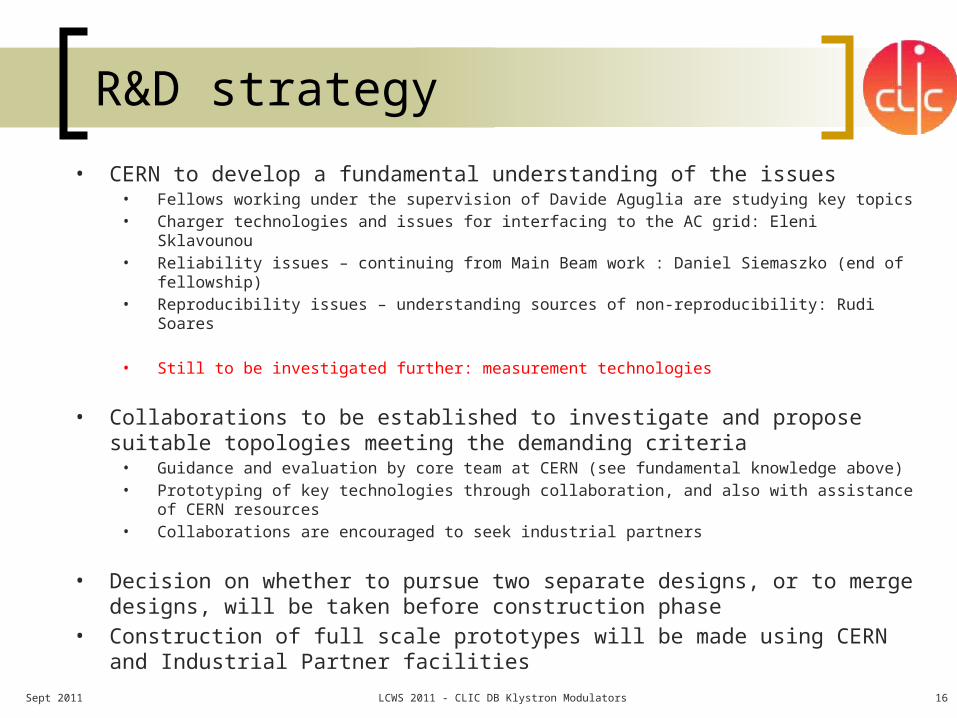
Sept 2011 LCWS 2011 - CLIC DB Klystron Modulators 16
• CERN to develop a fundamental understanding of the issues• Fellows working under the supervision of Davide Aguglia are studying key topics• Charger technologies and issues for interfacing to the AC grid: Eleni Sklavounou• Reliability issues – continuing from Main Beam work : Daniel Siemaszko (end of fellowship)• Reproducibility issues – understanding sources of non-reproducibility: Rudi Soares
• Still to be investigated further: measurement technologies
• Collaborations to be established to investigate and propose suitable topologies meeting the demanding criteria
• Guidance and evaluation by core team at CERN (see fundamental knowledge above)• Prototyping of key technologies through collaboration, and also with assistance of CERN resources• Collaborations are encouraged to seek industrial partners
• Decision on whether to pursue two separate designs, or to merge designs, will be taken before construction phase
• Construction of full scale prototypes will be made using CERN and Industrial Partner facilities

Invite proposals
Sept 2011 LCWS 2011 - CLIC DB Klystron Modulators 17
•Paper written and presented to Pulsed Power community in June 2011 summarizing the challenges
• Klystron Modulator Technology Challenges for the Compact Linear Collider (CLIC)
•Collaboration agreed with University of LAVAL, Quebec, Canada• To study resonant topologies and their suitability for the CLIC project
• In particular, demonstrate that a sufficiently fast rise time can be achieved• Demonstrate the magnetic technologies that are required (fast rise time
pulse transformers, high frequency resonant transformers)• Design appropriate prototype assemblies

Invite proposals
Sept 2011 LCWS 2011 - CLIC DB Klystron Modulators 18
•A number of other collaborations are under discussion•ETH Zurich, CH
• Has already developed a short pulse modulator for PSI.• Currently engaged in work for pulsed precision measurements.• The high voltage group has all the qualities we need from a research partner.• Discussions in progress – hope to conclude collaboration agreement in the coming
months with emphasis on topologies and global optimization.
•SLAC, USA• Power research group has worked extensively on Marx topologies for ILC.• End of ILC research project this year.• modulator and klystron development team interested in being involved.• SLAC will prepare a white paper to summarize the contribution that can be made.
•Los Alamos National Laboratories, USA• Has already built (with difficulty) a high power, resonant modulator for SNS.• They have worked with Nottingham University on some studies.• Studies into a split-core transformer topology to be investigated; manpower
contribution offered; cost to be evaluated.

EPC internal organisation
Sept 2011 LCWS 2011 - CLIC DB Klystron Modulators 19
http://te-epc-lpc.web.cern.ch/te-epc-lpc/machines/clic/general.stm

Conclusion
Sept 2011 LCWS 2011 - CLIC DB Klystron Modulators 20
•Promising progress on collaboration agreements for modulator topology studies
•More effort needed on measurement technologies How to measure HV pulses with ppm precision?
•Relaxation of reproducibility requirements are welcome.
•Modulator testbeds need to be planned Test area on passive load for power development Test area on klystron load for pulse measurement and feedback
studies (CLIC 0?)