Semiconductor Detectors - Astronomypetra/phys6771/lecture11.pdf · 2005-11-22 · Semiconductor...
21
Semiconductor Detectors
Transcript of Semiconductor Detectors - Astronomypetra/phys6771/lecture11.pdf · 2005-11-22 · Semiconductor...

Semiconductor Detectors

Summary of Last Lecture
Band structure in Solids:
Conduction band
Valence band
Insulator
Eg > 5 eV
Conduction band
Valence band
Semiconductor
Eg ~ 2 eV
thermalconductivity:
ni=AT e
T absolute temperatureK Boltzmann constantA material constantEg band gap
-Eg/(2kT)3/2
room temperature:pure Si: 1.5 x 10¹⁰/cm3
pure Ge: 2.5 x 10¹³/cm3Charge carrier in conductor: e-
Charge carrier in semiconductor: e-, holes

Summary of Last LectureAcceptor (e.g. B in Si):
p-type Si(extra holes
=majority charge carriers)
Donor (e.g. P in Si):n-type Si
(extra electrons= majority charge carriers)
Conduction band
Valence band
Semiconductor
Eg ~ 1 eVextra
Levelsintroduced
Conduction band
Valence band
Semiconductor
Eg ~ 1 eV
Doping

Summary of Last LectureSemiconductor Junction: np
• Rectifying diode• Initial diffusion of holes
towards the n-region and e-towards the p-region [a), b)]
• Charge build-up on either side of the junction [c)]
• p-region → negativen-region → positive [c)]
• Electric field gradient across the junction → process halted → region of immobile space charge [d)]
• Due to electric field: potential difference across the junction → contact potential V0 (~1V)
holes
e-
Region of changing potential:depletion zone or space charge region

Summary of Last LectureReversed bias junction
• pn junction:1) intrinsic electrical field not
intense enough to provideefficient charge collection
2) thickness of depletion zoneonly sufficient for stoppinglowest energy particles
• apply reverse bias voltage to junction, i.e. a negative voltage on the p-side:→ attracts holes in the p-region
( “ e- “ “ n-region)→ enlarge depletion zone→ “ sensitive volume
1. d ~ √Vb2. the higher Vb, the
higher the charge collection efficiency

Summary of last lecturePhysics – device characteristics
• In general: depletion zone extends further into the light doped side
• Depletion zone• Contact/depletion
voltage• Resistivitiy
qNeffd V biasε2= ☼
ε2
2DNV
qefffd =
)(1
NN ppnnq µµ
ρ+
=
=µ he,=Neff
electron, hole mobility
Effective carrier concentration
x = distance from junction D = silicon thickness
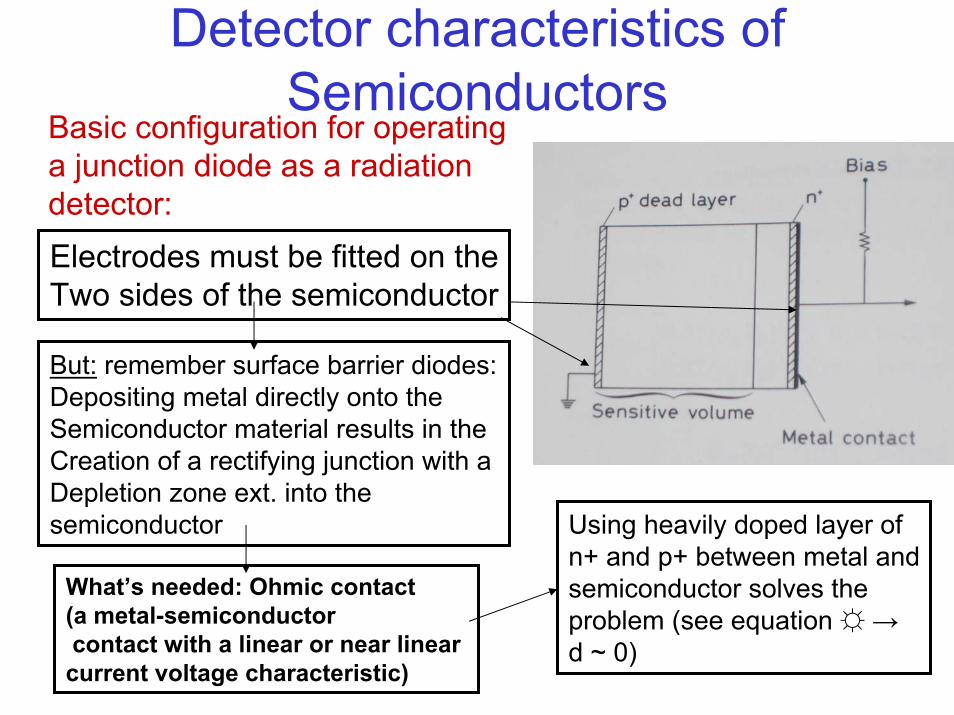
Detector characteristics of Semiconductors
Basic configuration for operatinga junction diode as a radiation detector:Electrodes must be fitted on theTwo sides of the semiconductor
But: remember surface barrier diodes:Depositing metal directly onto the Semiconductor material results in the Creation of a rectifying junction with a Depletion zone ext. into the semiconductor Using heavily doped layer of
n+ and p+ between metal andsemiconductor solves the problem (see equation ☼ →d ~ 0)
What’s needed: Ohmic contact (a metal-semiconductorcontact with a linear or near linear current voltage characteristic)

Average Energy per Electron-Hole Pair
• The average energy for creating a electron-hole pair at a given temperature is independent of the type and energy of the radiation and only dependent on the material
• Number of charge carriers is almost an order of magnitude higher than in gases
• Compared to the number of photo electrons in a scintillation counter the number of charge carriers are almost two orders of magnitude higher→ greatly improved energy
resolution
2.96 eV3.81 eV77 K
3.62 eV300 K
GeSi
Energy gaps are only ~ 1 eV
Where do the other two thirdsOf the energy go?
Lattice vibrations

Linearity• If depletion region is sufficiently thick to completely stop all
particles → semiconductor response ~ E• If E energy of radiation E/w electron-hole pairs should be
produced, w average energy from table before• Voltage observed at the electrodes:
V = Q/C = n E/ (w C), C capacitance of semiconductor, w average energy, n charge collection efficiency → V ~ E
• w independent of type of radiation → E independent of type of radiation (only true for lightly ionizing particles such as electrons and positrons, plasma effects occur for heavier ions)
If depletion zone is smaller → nonlinear response (not the fullEnergy is deposited);Instead the energy loss ∆E is measured, which is a non-linear Function of energy
Leakage current• Reversed bias diode is ideally nonconduction, but a
small fluctuating current flows through the semiconductor when a voltage is applied → noise
• Sources of leakage current:– Movement of minority charges (e.g. holes from the n-region
attracted across the junction to p-region), ~ nA/cm2
– Thermally generated electron-hole pairs originating from the recombination and trapping centers in the depletion region (depends on the absolute number of traps), ~µA/cm2
– Leakage current through the surface channels (depends on very many factors, e.g. the surface chemistry, contaminants, surrounding atmosphere, etc.)minimize by clean encapsulation

Sensitivity and Intrinsic Efficiency
• Intrinsic detection efficiency close to a 100% for charged particles (as very few particles will fail to create some ionization in the sensitive volume)limiting factors: leakage current in the detector and noise from the associated electronics →sets lower limit on the pulses which can be detected
• Ensure adequate signal: depletion depth sufficiently thick → S (ioniz) > S (noise)
• Energy measurements: d > particle range

Sensitivity
Leo, page 230

Gamma Ray Detection
• Germanium is preferred over silicon because of higher Z
• However because of the smaller band gap, leakage current in Ge to high at room temperatures → Ge must be cooled (liquid nitrogen)
• For low energies below ~ 30 keV silicon detectors are preferred because the K-edge in Ge is located at ~11 keV

Comparison of NaI detector and Ge detector for Co-60

Energy Measurement:Energy resolution: # of information carriers:
Scintillator: > 100 eV / photon Gas: 20 – 40 eV / chargeSilicon: 3.6 eV / chargeGermanium: 2.8 eV / charge
Silicon advantages:• low ionization energy (good signal)• long mean free path (good charge collection efficiency)• high mobility (fast charge collection)• low Z (low multiple scattering)• production technologies very well developedGermanium: higher Z detect γ radiation (needs cooling…)

Diffused Junction Diodes
• Among the first fabricated• Produced by diffusing n-type impurities such
as phosphorus into one end of a homogeneous p-type semiconductor at high temperatures (~1000 deg C)
• By adjusting concentrations and diffusion time → junctions lying at a depths of few tenths of a microns to two microns can be produced
Ion-Implanted Diodes
• Formed by bombarding the semiconductor crystal with a beam of impurity ions from an accelerator
• By adjusting the beam energy, the impurity concentration and depth profile can be controlled
• Since radiation damage is incurred, the semiconductor must be annealed at temperatures of 500 deg C

Surface Barrier Diode
See previous lecture

Position Sensitive Detector
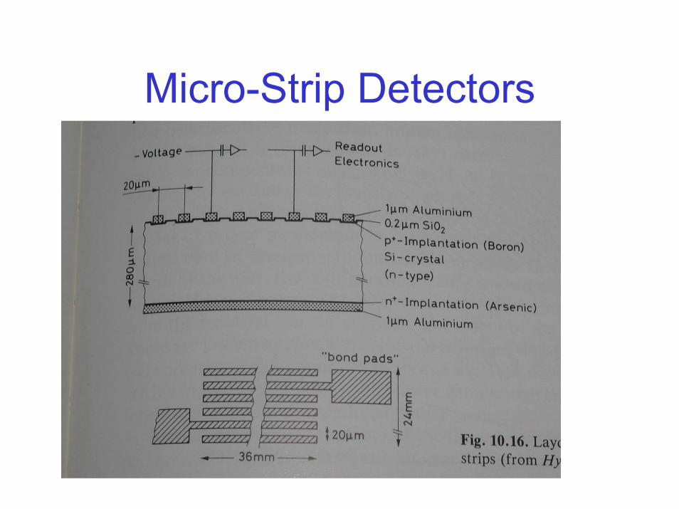
Micro-Strip Detectors

Applications
• CCD detectors• APS detectors• Micro vertex detectors• More about those later