Semiconductor detectors - IJSkrizan/sola/efjod/slides/semiconductor-detectors.pdf · Semiconductor...
42
V. Cindro and P. Križan, IJS and FMF Semiconductor detectors 1 Semiconductor detectors •properties of semiconductors •p-i-n diode •interface metal-semiconductor •measurements of energy •space sensitive detectors •radiation damage in detectors Literatura: W.R.Leo: Techniques for Nucear and Particle Physics Experiments H. Spieler: Semiconductor Detector Systems G. Lutz: Semiconductor Radiation Detectors S.M. Sze: Physics of Semiconductor Devices Glenn F. Knoll: Radiation Detection and Measurement
Transcript of Semiconductor detectors - IJSkrizan/sola/efjod/slides/semiconductor-detectors.pdf · Semiconductor...

V. Cindro and P. Križan, IJS and FMF
Semiconductor detectors 1
Semiconductor detectors•properties of semiconductors•p-i-n diode •interface metal-semiconductor •measurements of energy •space sensitive detectors•radiation damage in detectors
Literatura:W.R.Leo: Techniques for Nucear and Particle Physics ExperimentsH. Spieler: Semiconductor Detector Systems G. Lutz: Semiconductor Radiation DetectorsS.M. Sze: Physics of Semiconductor DevicesGlenn F. Knoll: Radiation Detection and Measurement

V. Cindro and P. Križan, IJS and FMF
Semiconductor detectors 2
• Energy resolution of a detector depends on statistical fluctuation in the number of free charge carriers that are generated during particle interaction with the detector material
• Low energy needed for generation of free charge carriers → good resolution
• Gas based detectors: a few 10eV, scintillators: from a few 100 do to 1000 eV
• Semiconductors: a few eV!
Why semiconductors?

V. Cindro and P. Križan, IJS and FMF
Semiconductor detectors 3
Comparison: radiation spectrum as measured with a Ge (semiconductor) in NaI (scintillation) detector

V. Cindro and P. Križan, IJS and FMF
Semiconductor detectors 4
good energy resolution → easier signal/background sepairstion
V. Cindro and P. Križan, IJS and FMF
Semiconductor detectors 5
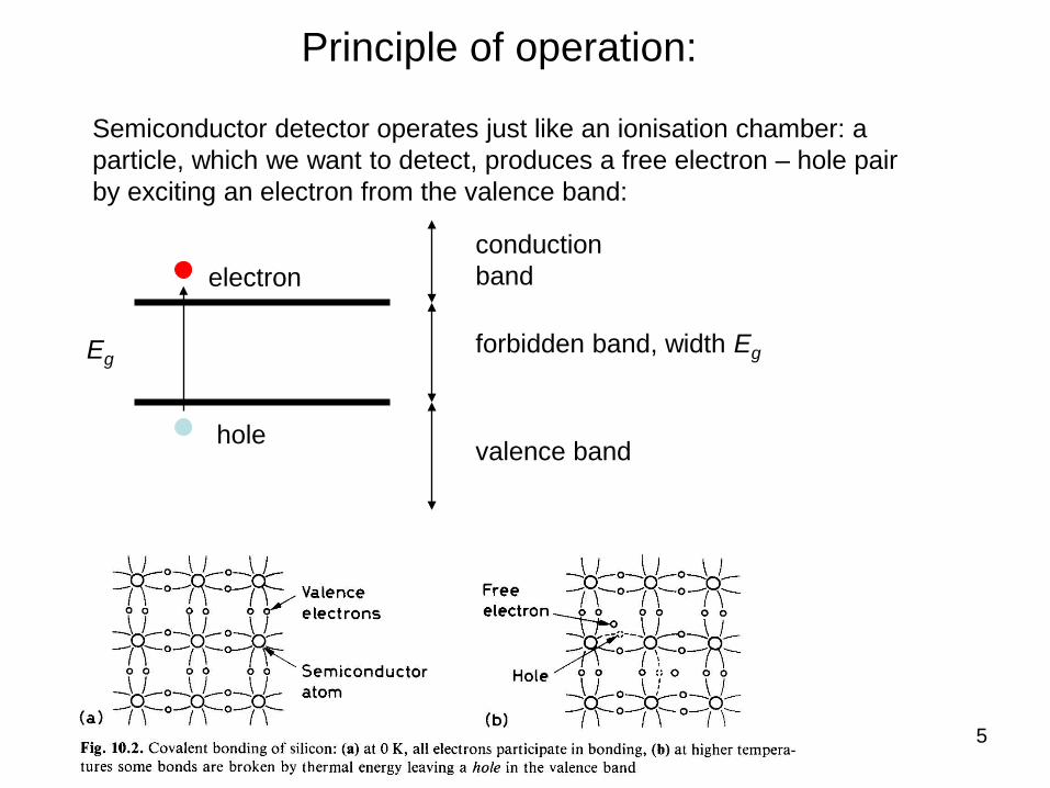
Principle of operation:
Semiconductor detector operates just like an ionisation chamber: a particle, which we want to detect, produces a free electron – hole pair by exciting an electron from the valence band:
electron
hole
Egforbidden band, width Eg
conduction band
valence band

V. Cindro and P. Križan, IJS and FMF
Semiconductor detectors 6
Drift velocity in electric field:
Evd ×= µ
Evd ⋅= µµ mobility
different for electrons and for holes!
V. Cindro and P. Križan, IJS and FMF
Semiconductor detectors 7
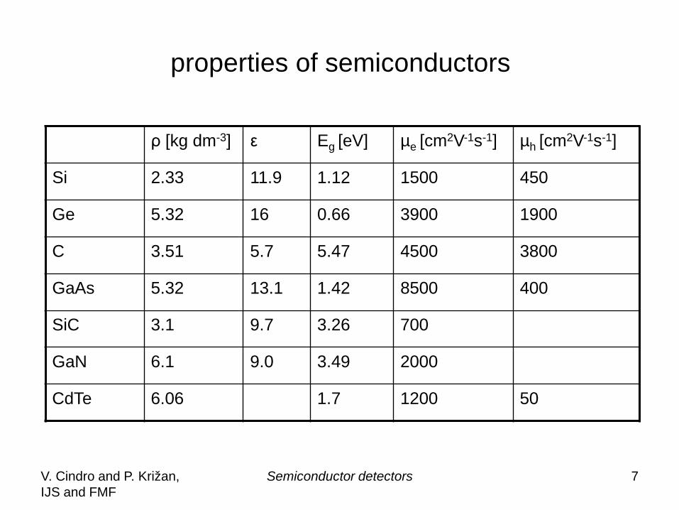
properties of semiconductors
ρ [kg dm-3] ε Eg [eV] µe [cm2V-1s-1] µh [cm2V-1s-1]
Si 2.33 11.9 1.12 1500 450
Ge 5.32 16 0.66 3900 1900
C 3.51 5.7 5.47 4500 3800
GaAs 5.32 13.1 1.42 8500 400
SiC 3.1 9.7 3.26 700
GaN 6.1 9.0 3.49 2000
CdTe 6.06 1.7 1200 50

V. Cindro and P. Križan, IJS and FMF
Semiconductor detectors 8
n - concentration of conduction electrons
p - concentration of holes
∫=t
c
E
E
dEEFENn )()(
N(E) density of states
)exp(1
1)(
kTEEEF
F−+=
Fermi-Dirac distribution
EF Fermi energy level
Pure semiconductorNeutrality: n=p
)ln(4
32 e
hvcF
mmkTEEE +
+= ratio of effective masses of holes
and electrons
Intrinsic (pure) semiconductor (no impurities)

Semiconductor detectors 9
)exp(
))(exp(
))(exp(
2
kTE
NNnpn
kTEENp
kTEENn
gvci
vFv
Fcc
−==×
−−×=
−−×=
)2
exp(kTE
NNn gvei −=
[ ][ ]
322
313
310
atoms 10 ofout
104.2
104.1
−
−
−
×=
×=
cmGecmnSicmn
i
i
Ec energy of the bottom of conduction bandEv energy of the top of the valence bandEg =Ec-Ev width of the forbidden band
Nc, Nv: effective density of states in the conduction and valence bands
At room themperature:
ni number density of free charge carriers in an intrinsic semiconductor (only for electrons and holes)
V. Cindro and P. Križan, IJS and FMF
Semiconductor detectors 10
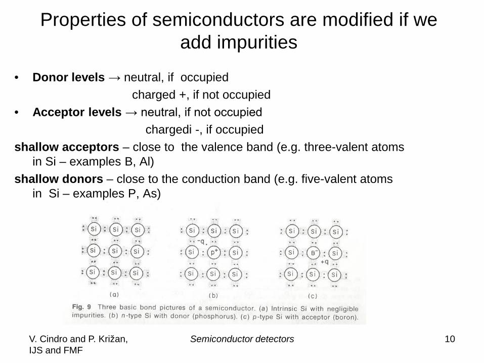
Properties of semiconductors are modified if we add impurities
• Donor levels → neutral, if occupiedcharged +, if not occupied
• Acceptor levels → neutral, if not occupiedchargedi -, if occupied
shallow acceptors – close to the valence band (e.g. three-valent atoms in Si – examples B, Al)
shallow donors – close to the conduction band (e.g. five-valent atoms in Si – examples P, As)
V. Cindro and P. Križan, IJS and FMF
Semiconductor detectors 11
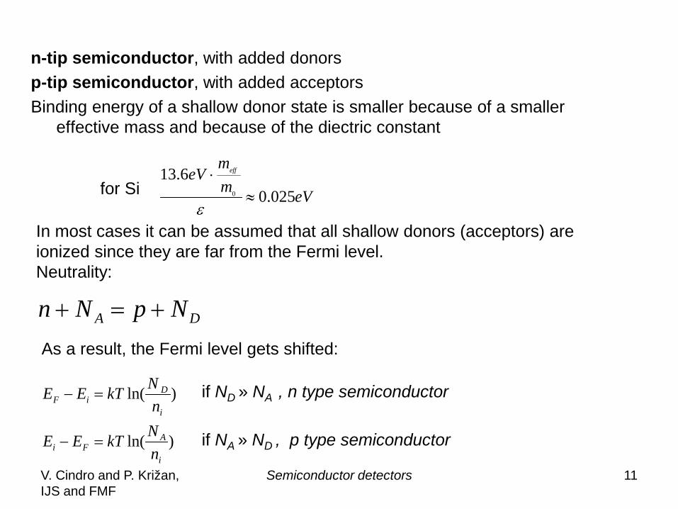
n-tip semiconductor, with added donorsp-tip semiconductor, with added acceptors Binding energy of a shallow donor state is smaller because of a smaller
effective mass and because of the diectric constant
eVmm
eV eff
025.06.13
0 ≈⋅
εfor Si
In most cases it can be assumed that all shallow donors (acceptors) areionized since they are far from the Fermi level. Neutrality:
DA NpNn +=+As a result, the Fermi level gets shifted:
)ln(
)ln(
i
AFi
i
DiF
nNkTEE
nNkTEE
=−
=− if ND » NA , n type semiconductor
if NA » ND , p type semiconductor
V. Cindro and P. Križan, IJS and FMF
Semiconductor detectors 12
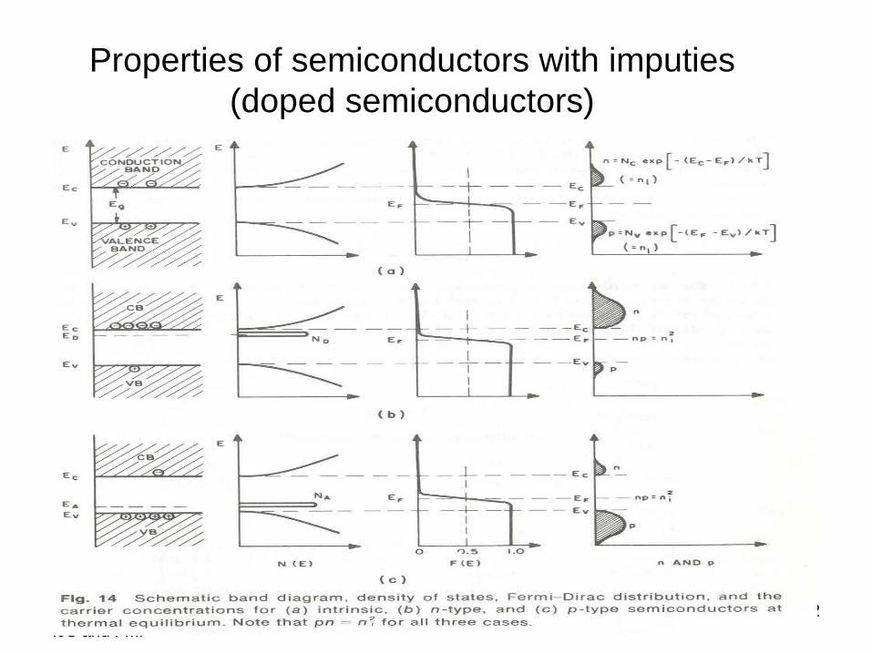
Properties of semiconductors with imputies (doped semiconductors)
V. Cindro and P. Križan, IJS and FMF
Semiconductor detectors 13
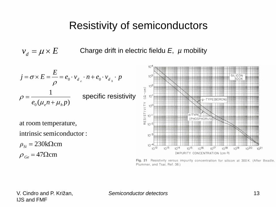
Resistivity of semiconductors
Evd ×= µ
cm47 cm230k
:torsemiconduc intrinsic re, temperaturoomat
)(
1
0
00
Ω=Ω=
+=
⋅⋅+⋅⋅==×=
Ge
Si
he
dd
ρ
pne
pvenveEEjhe
ρ
µµρ
ρσ
Charge drift in electric fieldu E, µ mobility
specific resistivity
V. Cindro and P. Križan, IJS and FMF
Semiconductor detectors 14
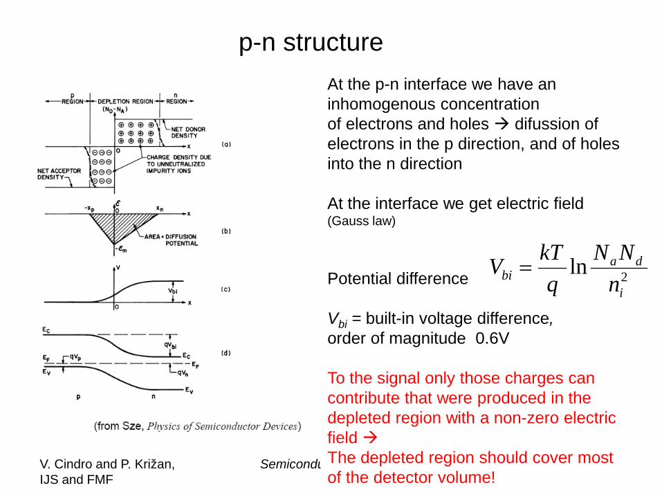
p-n structureAt the p-n interface we have an inhomogenous concentration of electrons and holes difussion of electrons in the p direction, and of holes into the n direction
At the interface we get electric field (Gauss law)
Potential difference
Vbi = built-in voltage difference, order of magnitude 0.6V
To the signal only those charges can contribute that were produced in the depleted region with a non-zero electric field The depleted region should cover most of the detector volume!
2lni
dabi n
NNq
kTV =
V. Cindro and P. Križan, IJS and FMF
Semiconductor detectors 15
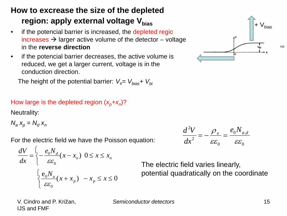
How to excrease the size of the depleted region: apply external voltage Vbias
• if the potencial barrier is increased, the depleted region increases larger active volume of the detector – voltage in the reverse direction
• if the potencial barrier decreases, the active volume is reduced, we get a larger current, voltage is in the conduction direction.
The height of the potential barrier: VB= Vbias+ Vbi
How large is the depleted region (xp+xn)?Neutrality:Na xp = Nd xn
For the electric field we have the Poisson equation: 0
,0
02
2
εεεερ dae Ne
dxVd
=−=
0 )(e
0 )(
0
0
0
0
≤≤−+
≤≤−−=
xxxxN
xxxxNedxdV
ppa
nnd
εε
εε The electric field varies linearly,potential quadratically on the coordinate
+ Vbias

V. Cindro and P. Križan, IJS and FMF
Semiconductor detectors 16
( ) 2/10
2/1
0
0
2/1
0
0
2/1
0
0
2/1
0
0
2
:y resistivit spec. theof in terms
2 :example
)(2
)/1(2
))/1(
2(
biasen
d
biasnda
da
dabiaspn
daa
biasp
add
biasn
Vd
NeVxdNN
NNNN
eVxxd
NNNeVx
NNNeVx
µρεε
ρ
εε
εε
εε
εε
≈
≈≈⇒>>
+=+=
+
=
+=
increases as Vbias1/2
example: silicon
=type-p m )0.32(
type-n m )(53.02/1
p
2/1
µρ
µρ
bias
biasn
VV
dif ρ=20000kΩcm andVbias=1 V → d~75µm

V. Cindro and P. Križan, IJS and FMF
Semiconductor detectors 17
Leakage current
= current in the reverse direction
difussion current: • difussion of minority carriers into the region with electric field• current of majority carriers with large enough thermic energy, such
that they overcome the potencial barrier
generation current: generation of free carriers with the thermal excitation in the depleted layer

V. Cindro and P. Križan, IJS and FMF
Semiconductor detectors 18
The probability of excitation is dramatically increased in the presence of intermediate levels.

V. Cindro and P. Križan, IJS and FMF
Semiconductor detectors 19
generation current:
trapsofion concentrat )2
exp(2t
gtgen N
kTE
TNj −∝
→ high T – high generation current→ wider forbidden band Eg , lower generation current
Consequence: some detectors have to be cooled (Ge based, radiation damaged silicon detectors)

V. Cindro and P. Križan, IJS and FMF
Semiconductor detectors 20
metal-semiconductor interface (Schottky barrier)
Χ electron affinity
Φ work function
Assumption Φm >Φs
Vbi = Φm- Φs

V. Cindro and P. Križan, IJS and FMF
Semiconductor detectors 21
No external voltage
voltage in the conduction direction
voltage in the reverse direction
Ohmic contact: high concentration of impurities → thin barrier → tuneling
V. Cindro and P. Križan, IJS and FMF
Semiconductor detectors 22
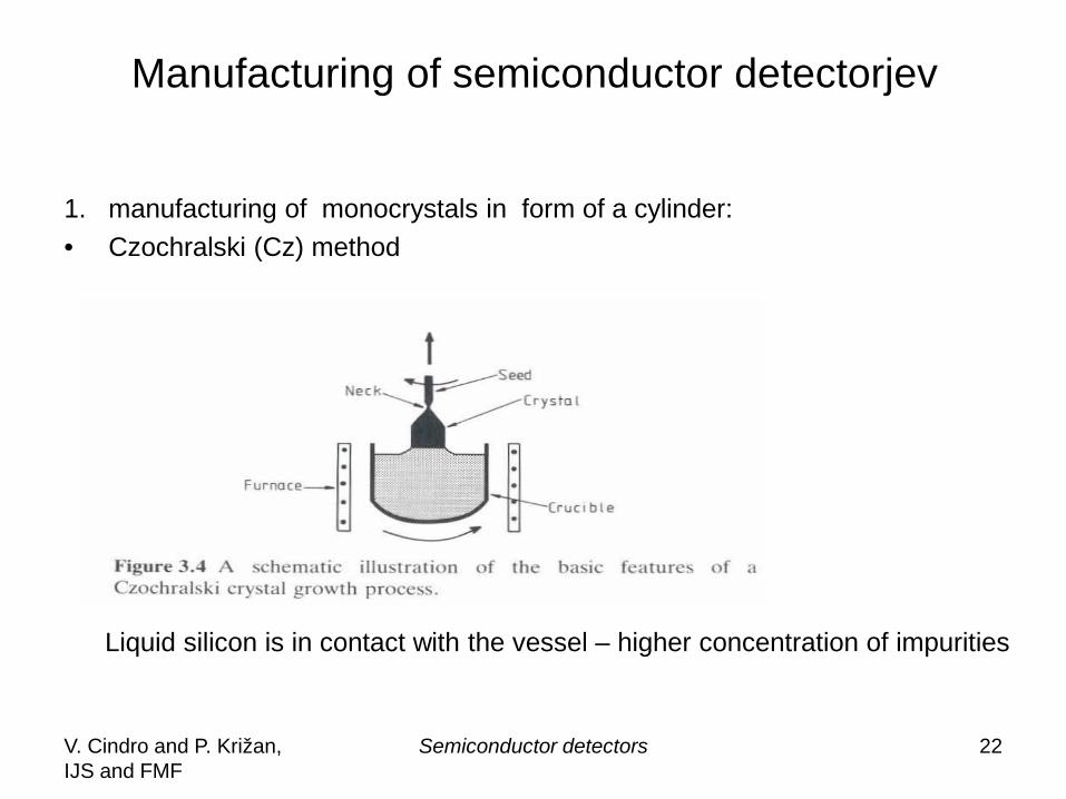
Manufacturing of semiconductor detectorjev
1. manufacturing of monocrystals in form of a cylinder:• Czochralski (Cz) method
Liquid silicon is in contact with the vessel – higher concentration of impurities

V. Cindro and P. Križan, IJS and FMF
Semiconductor detectors 23
Float zone method:
No contact of the liquid semiconductor with the walls –higher purity of the material.

V. Cindro and P. Križan, IJS and FMF
Semiconductor detectors 24
Photolitography for pattern fabrication

June 5-8, 2006 Course at University of Tokyo
50 cm
20 cm
Two coordinates measured at the same timeTypical strip pitch ~50µm, resolution about ~15 µm
pitch
Typical tracking device in particle physics: silicon strip detector

V. Cindro and P. Križan, IJS and FMF
Semiconductor detectors 26
Signal development in a semiconductor detector1. interaction of particles with matter (generation of electron – hole pairs)
2. drift of charges in electric field causes an induced current on the electrodes (signal) – similar as in the ionisation detector
96.0 6.11
1) Zparticle, ionizing (minimum M.I.P.for
2 ≈=≈
=∝
− cv
gcmMeV
dxdE
AZ
dxdE
ion
βρ
ρ
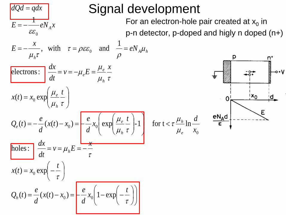
Signal development For an electron-hole pair created at x0 in p-n detector, p-doped and higly n doped (n+)
−−−=−=
−=
−===
<
−=−−=
=
=−==
==−=
−=
=
τ
τ
τµ
µµτ
τµµ
τµµ
τµµµ
µρ
ρεεττµ
εε
txdextx
detQ
txtx
xEvdtdx
xdtx
dextx
detQ
txtx
xEvdtdx
eNxE
xeNE
qdxdQd
h
h
e
h
h
ee
h
e
h
ee
hAh
A
exp1))(()(
exp)(
:holes
ln for t 1-exp))(()(
exp)(
:electrons
1 and with ,
1
00
0
000
0
0
0

Signal development 2
Relation between charge carrier propagation and induced current:
detector volume V=S*dn = concentration of carriers
I=j*S current through surface SI=e0*v*n*S
For a single drifting electron: n*V=n*S*d=1 n*S=1/d
and therefore for a single drifting electron we get:I=e0*v/dand dQ*d = e0*dx

Signal development 3 For an electron-hole pair created at x0
−−−=−=
<
−=−−=
τ
µµτ
τµµ
txdextx
detQ
xdtx
dextx
detQ
e
e
h
h
ee
exp1))(()(
:holes
ln for t 1-exp))(()(
:electrons
00
000

V. Cindro and P. Križan, IJS and FMF
Semiconductor detectors 30
Number of pairs/cm
ε (eV)
Si 3.87 1.07 106 3.61
Ge 7.26 2.44 106 2.98
C 3.95 0.246 106 16
gas ~keV/cm a few 100 ~30
Scint. ~300-1000/ph.e.
[ ]cmMeVdxdE
//
Si on average ~100 electron-hole pairs /µm

Semiconductor detectors 31
Radiation damageDamage caused by:• Bulk effect: lattice damage, vacancies and interstitials• Surface effects: Oxide trap charges, interface traps.
C. oram, Academic training, CERN, 2002J

Semiconductor detectors 32
Main radiation induced macroscopic changes
How to mitigate these effects?• Geometry: build sensors such that they stand high depletion voltage (500V)• Environment: keep sensors at low temperature (< -10ºC) Slower reverse
annealing. Lower leakage current.C. oram, Academic training, CERN, 2002J

V. Cindro and P. Križan, IJS and FMF
Semiconductor detectors 33
Absorption of gamma rays
• Photoeffect
)( 1
)( 1
25
22/7
5
cmEE
Z
cmEEE
Z
eph
eKph
>>∝
<<∝
γγ
γ
σ
σγ
• Compton scattering
Z∝σ
• Pair production 2Z∝σ
gamma ray photo-electron

V. Cindro and P. Križan, IJS and FMF
Semiconductor detectors 34

V. Cindro and P. Križan, IJS and FMF
Semiconductor detectors 35

V. Cindro and P. Križan, IJS and FMF
Semiconductor detectors 36

Germanium detectors
V. Cindro and P. Križan, IJS and FMF
Semiconductor detectors 37

V. Cindro and P. Križan, IJS and FMF
Semiconductor detectors 38
Energy resolution of gamma detectors
Depends on the statistical fluctuation in the number of generated electron-hole pairs.
If all energy of the particle gets absorbed in the detector – E0 (e.g. gamma ray gets absorbed via photoeffect, and the photoelectron is stopped):
on average we get
generated pairs
0_
ii
ENε
=
εi ~ 3.6eV for Si~ 2.98 eV for Ge
Average energy needed to create an e-h pair
gamma ray photo-electron

V. Cindro and P. Križan, IJS and FMF
Semiconductor detectors 39
V. Cindro and P. Križan, IJS and FMF
Semiconductor detectors 40
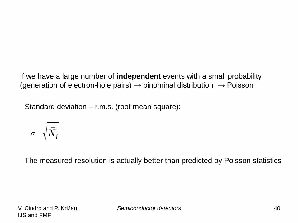
If we have a large number of independent events with a small probability (generation of electron-hole pairs) → binominal distribution → Poisson
iN__
=σ
Standard deviation – r.m.s. (root mean square):
The measured resolution is actually better than predicted by Poisson statistics
V. Cindro and P. Križan, IJS and FMF
Semiconductor detectors 41
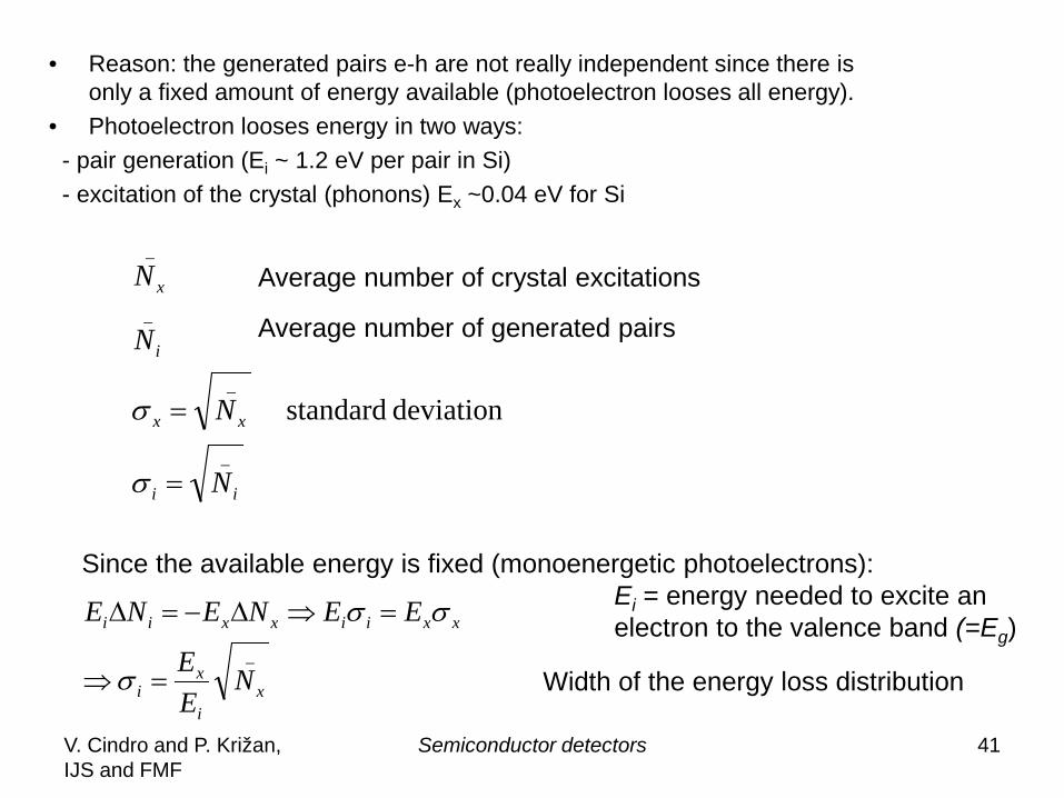
• Reason: the generated pairs e-h are not really independent since there is only a fixed amount of energy available (photoelectron looses all energy).
• Photoelectron looses energy in two ways: - pair generation (Ei ~ 1.2 eV per pair in Si)- excitation of the crystal (phonons) Ex ~0.04 eV for Si
_
_
_
_
deviation standard
ii
xx
i
x
N
N
N
N
=
=
σ
σ
Average number of crystal excitations
Average number of generated pairs
Since the available energy is fixed (monoenergetic photoelectrons):Ei = energy needed to excite an electron to the valence band (=Eg)
_
xi
xi
xxiixxii
NEE
EENENE
=⇒
=⇒∆−=∆
σ
σσ
Width of the energy loss distribution
V. Cindro and P. Križan, IJS and FMF
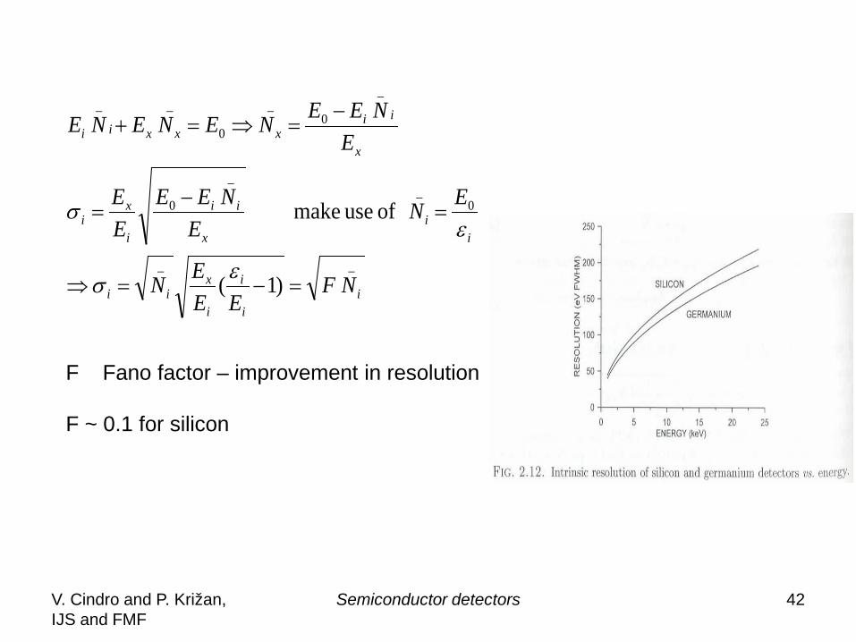
Semiconductor detectors 42
__
0_
_
0
_
0_
0
__
)1(
of use make
ii
i
i
xii
ii
x
ii
i
xi
x
iixxxii
NFEE
EN
ENE
NEEEE
ENEENENENE
=−=⇒
=−
=
−=⇒=+
εσ
εσ
F Fano factor – improvement in resolution
F ~ 0.1 for silicon