SEMI Test Methods under Development Peter Wagner Test Methods... · SEMI Test Methods under...
20
SEMI Test Methods under Development for Si Feedstock Materials, Bricks and Wafers Peter Wagner
Transcript of SEMI Test Methods under Development Peter Wagner Test Methods... · SEMI Test Methods under...

SEMI Test Methods under Development
for Si Feedstock Materials, Bricks and
Wafers Peter Wagner
Background
• SEMI Test Methods are an essential part of SEMI
Standards.
• They are referenced in material specifications.
• They help to establish common understanding
• of metrics,
• of measurement procedures and
• of measurement results.
• So far, 7 out of 33 published SEMI PV Standards are Test Methods
• Several new test methods are currently developed
Workshop on Test Methods for Si Feedstock
Materials, Bricks and Wafers, Munich, June 2012 2

Published SEMI Test Methods
• SEMI PV1-0211, Test Method for Measuring Trace Elements in PV-Grade Si by
High-Mass Resolution Glow Discharge Mass Spectrometry
• SEMI PV9-0611, Test Method for Excess Charge Carrier Decay in PV Si
Materials by Non-Contact Measurement of Microwave Reflectance after a Short
Illumination Pulse
• SEMI PV10-1110, Test Method for Instrumental Neutron Activation Analysis
• SEMI PV13-1111, Test Method for Contactless Excess-Charge-Carrier
recombination Lifetime Measurement in Si Wafers, Ingots, and Bricks Using an
Eddy-Current Sensor
• SEMI PV23-1011, Test Method for Mechanical Vibration of Crystalline Si PV
Modules in Shipping Environment
• SEMI PV25-1011, Test Method for Simultaneously Measuring Oxygen, Carbon,
Boron and Phosphorous in Solar Si Wafers and Feedstock by Secondary Ion
Mass Spectrometry
• SEMI PV28-0212, Test Method for Measuring Resistivity or Sheet Resistance
with a Single-Sided Noncontact Eddy-Current Gauge
Workshop on Test Methods for Si Feedstock
Materials, Bricks and Wafers, Munich, June 2012 3

Test Methods under Development(1)
• Doc 5330, NEW STANDARD: TEST METHOD FOR IN-LINE MEASUREMENT
OF CRACKS IN PV SILICON WAFERS BY DARK FIELD INFRARED IMAGING
(EU, passed technical review)
• Doc 5331A, NEW STANDARD: TEST METHOD FOR IN-LINE MEASUREMENT
OF SAW MARKS ON PV SILICON WAFERS BY A LIGHT SECTIONING
TECHNIQUE USING MULTIPLE LINE SEGMENTS (EU, passed technical
review)
• Doc 5332A, NEW STANDARD: TEST METHOD FOR IN-LINE MEASUREMENT
OF THICKNESS AND THICKNESS VARIATION OF SILICON WAFERS FOR
PV APPLICATIONS USING CAPACITIVE PROBES (EU, passed technical
review)
• Doc 5333, NEW STANDARD: TEST METHOD FOR IN-LINE MEASUREMENT
OF WAVINESS OF PV SILICON WAFERS BY A LIGHT SECTIONING
TECHNIQUE (EU, ballot planned for July 2012)
Workshop on Test Methods for Si Feedstock
Materials, Bricks and Wafers, Munich, June 2012 4

Test Methods under Development(2)
• Doc 4675B, NEW STANDARD: TEST METHOD FOR THE MEASUREMENT OF
ELEMENTAL IMPURITY CONCENTRATIONS IN SILICON FEEDSTOCK FOR
SILICON SOLAR CELLS BY BULK DIGESTION, INDUCTIVELY COUPLED-
PLASMA MASS SPECTROMETRY (NA, drafting)
• Doc 5394, NEW STANDARD: TEST METHOD FOR QSS MICROWAVE PCD
MEASUREMENTS OF CARRIER DECAY AND LIFETIME (NA, drafting)
Workshop on Test Methods for Si Feedstock
Materials, Bricks and Wafers, Munich, June 2012 5

Planned New Activities
• Doc xxxx, NEW STANDARD, TEST METHOD FOR IN-LINE
CHARACTERIZATION OF PV SI WAFERS BY USING
PHOTOLUMINESCNCE( EU, drafting)
• Doc xxxx, NEW STANDARD, TEST METHOD FOR IN-INE
MEASUREMENT OF LATERAL DIMENSIONS OF SILICON WAFERS FOR
PV APPLICATIONS (EU, drafting)
• Doc xxxx, NEW STANDARD; TEST METHOD FOR IN-LINE
CHARACTERIZATION OF PV SILICON WAFERS REGARDING GRAIN
SIZE (EU, drafting)
Workshop on Test Methods for Si Feedstock
Materials, Bricks and Wafers, Munich, June 2012 6

Doc 5330, Purpose
• Silicon (Si) for PV applications contains a variety of micro- and macroscopic
crystallographic defects and flaws that may impact the efficiency of a solar
cells or the yield of a manufacturing line.
• Two categories of defects:
• Grown-in defects consisting of point defects (impurities, vacancies, self-
interstitials and their complexes), dislocations, grain boundaries, and
precipitates/inclusions.
• Process induced defects consisting of chips/indents (surface and edge) and
cracks (not to mention the surface itself).
• Inclusions, chips and cracks are detrimental for solar cell processing as they
may enhance stress in the wafer bulk and the region surrounding them and
trigger the breakage of a wafer.
• Defining a test method for reproducibly detecting and characterizing cracks
and distinguishing them from other defects to avoid quality issues and
improve claim handling.
Workshop on Test Methods for Si Feedstock
Materials, Bricks and Wafers, Munich, June 2012 7

Doc 5330, Scope
• This test method characterizes cracks in single or multi-crystalline Si
wafers.
• It covers an in-line, non-contacting and non-destructive method that
determines the number of cracks per wafer and crack length of clean, dry
as-cut Si wafers that are supported by two belts that move the test
specimen through the measurement equipment.
• This test method covers square and pseudo-square PV Si wafers, with a
nominal edge length ≥ 125 mm and a thickness ≥ 100 µm.
• Because this test method is intended for in-line high throughput
measurements it is mandatory to operate the measurement system under a
tight SPC (e.g. ISO 11462) for obtaining reliable, repeatable and
reproducible measurement data.
Workshop on Test Methods for Si Feedstock
Materials, Bricks and Wafers, Munich, June 2012 8

Doc 5330, Apparatus
Workshop on Test Methods for Si Feedstock
Materials, Bricks and Wafers, Munich, June 2012 9
digital line cameras
wafer transport direction
wafer
projector below wafer
projected light stripa
surface normal and line of sight of camera
projector besides waferprojector
besides wafer
Schematic drawing of the Set-up
for Measuring Cracks Showing
Projector Positions for Method A
(Projector below Wafer) and
Method B (Projectors besides
Wafer)

Doc 5330, Image Processing Steps
Workshop on Test Methods for Si Feedstock
Materials, Bricks and Wafers, Munich, June 2012 10
Edge detection and filtering
Detection of potential defects
Identification and
classification
of defects
SegmentationComparison
and final decision
Step 1 Step 2 Step 3 Step 4 Step 5
Outline of the Flow of the
Image Processing Steps

Workshop on Test Methods for Si Feedstock
Materials, Bricks and Wafers, Munich, June 2012
Doc 5331, Purpose
• Silicon (Si) wafers for PV applications cut from a Si ingot or Si brick by
multiple-wire sawing contain artifacts characteristic for this cutting
process, so called saw marks.
• Saw marks may significantly impact the quality of wafers. They interfere
with printing the contact fingers on solar cells. Extreme saw mark
dimensions may interrupt the contact fingers or create too wide fingers.
• Saw marks are frequently specified for Si wafers for solar cells with
respect to their maximum peak-to-valley within a finite distance, or
window.
• Standardized test methods providing reproducible values for saw marks
are required to specify this aspect of wafer quality.
• Process and quality control during manufacturing of wafers requires
continuous monitoring of saw marks with a non-contact method that
supports high throughput.
11

Workshop on Test Methods for Si Feedstock
Materials, Bricks and Wafers, Munich, June 2012
Doc 5331, Scope
• Determining maximum peak-to-valley of saw marks that typically run
across the entire wafer surface and along the wire direction.
• Applying to square and pseudo-square PV Si wafers, single and
multicrystalline, with a nominal edge length ≥ 125 mm and a nominal
thickness ≥ 100 µm.
• Intended for in-line, non-conctact, non-destructive high throughput
measurements. Therefore it is mandatory to operate the measurement
system under statistical process control (SPC, e.g. ISO 11462) in order
to obtain reliable, repeatable and reproducible measurement data.
• Based on a light sectioning technique where the saw marks are oriented
perpendicular to the direction of wafer transport.
12

Workshop on Test Methods for Si Feedstock
Materials, Bricks and Wafers, Munich, June 2012
Doc 5331, Apparatus
13
digital cameras
wafer transport direction
projector
wafer
projector
projected light line segment pattern A with two parallel
line segments
projected light line segment pattern A with a single line
segment
saw marks
scan line FLscan line FR
a
transport belts
D
Schematic View of the Upper
Part of the Measurement Set-
Up
Workshop on Test Methods for Si Feedstock
Materials, Bricks and Wafers, Munich, June 2012
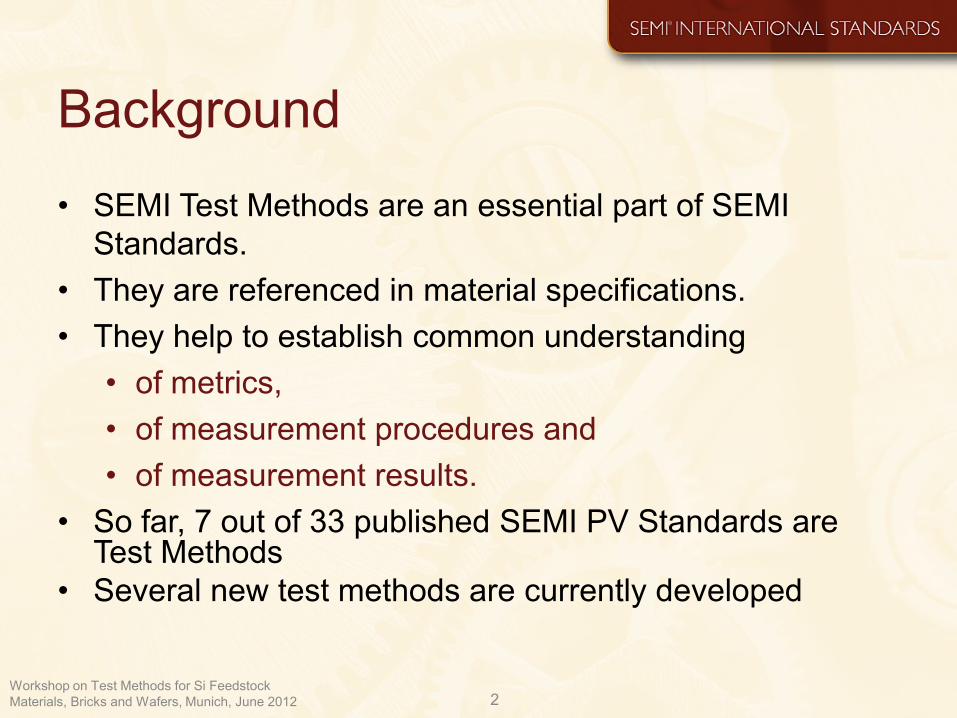
Doc 5331, Data Processing
14
x/a.u.
y/a.
u.
Image of light line segment
COB line and spline fit (dashed)
subtraction of spline fit from COB line
moving average filter
peak-to-valley evaluation -> ti,j,n(x)
maximum peak-to-valley
tth
Illustration of the Processing
Steps for Evaluating the Peak-to-
valley Value from the Digital
Image of the Light Line Trace

Workshop on Test Methods for Si Feedstock
Materials, Bricks and Wafers, Munich, June 2012
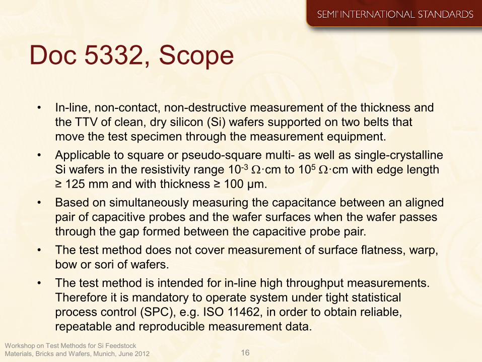
Doc 5332, Purpose
• Wafer thickness and its variation across a wafer are important
parameters for solar cell manufacturing. Excessive thickness variations
within a lot from wafer to wafer or within a wafer may negatively impact
process yield and solar cell efficiency.
• Both parameters are part of the specification for solar cell wafers (SEMI
PV22), which define a thickness range as well as an upper limit for the
total thickness variation (TTV).
• In addition, careful process and quality control of the wafer thickness and
its variation during wafer and solar cell manufacturing requires
continuous monitoring of thickness by the supplier of wafers for PV
applications as well as by the user of such wafers.
• Therefore a standardized test method providing reproducible data for
thickness and its variation is required to establish agreement between
business partners regarding the specification of wafers.
15
Workshop on Test Methods for Si Feedstock
Materials, Bricks and Wafers, Munich, June 2012
Doc 5332, Scope
• In-line, non-contact, non-destructive measurement of the thickness and
the TTV of clean, dry silicon (Si) wafers supported on two belts that
move the test specimen through the measurement equipment.
• Applicable to square or pseudo-square multi- as well as single-crystalline
Si wafers in the resistivity range 10-3 W·cm to 105 W·cm with edge length
≥ 125 mm and with thickness ≥ 100 µm.
• Based on simultaneously measuring the capacitance between an aligned
pair of capacitive probes and the wafer surfaces when the wafer passes
through the gap formed between the capacitive probe pair.
• The test method does not cover measurement of surface flatness, warp,
bow or sori of wafers.
• The test method is intended for in-line high throughput measurements.
Therefore it is mandatory to operate system under tight statistical
process control (SPC), e.g. ISO 11462, in order to obtain reliable,
repeatable and reproducible measurement data.
16

Workshop on Test Methods for Si Feedstock
Materials, Bricks and Wafers, Munich, June
2012
Doc 5332, Apparatus(1)
17
capacitive probe A
capacitive probe B
capacitive probe C
light sensors or emitters, respectively
light sensors or emitters, respectively
light sensors or emitters, respectively
waferwafer transport direction
CL = SL b
l1 l1
SL a
l3
l3
l2 l2
SL c
Schematic Drawing of
the Set-Up of the
Capacitive Probes, Top
View of the Bottom
Probes. The Gray
Areas Depict the Active
Areas of the Capacitive
Probes.

Workshop on Test Methods for Si Feedstock
Materials, Bricks and Wafers, Munich, June 2012
Doc 5332, Apparatus(2)
18
wafer transport direction
l3+e l3+e
l3+e l3+e
l3
l3
CL = SL b
SL a
CL
l2l2
SL c
OD
OD
OD
OD
OD
OD
Measurement Positions for 5- Point
(Triangles) and 9- Point (Circles)
Measurements. The Crosses Depict the
First and Last Measurement Points as
well as the Center Points on the Scan
Lines.
Workshop on Test Methods for Si Feedstock
Materials, Bricks and Wafers, Munich, June 2012
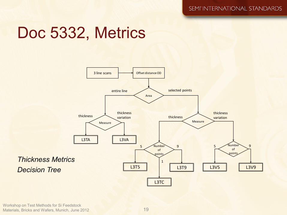
Doc 5332, Metrics
19
L3TA
Area
Measure Measure
thicknessthickness variation
entire line selected points
L3T5
Number of
points
L3TC
L3T9
thicknessthickness variation
L3VANumber
of points
L3V5 L3V9
5 59 9
1
Offset distance OD3 line scans
Thickness Metrics
Decision Tree
Workshop on Test Methods for Si Feedstock
Materials, Bricks and Wafers, Munich, June 2012 20
THANK YOU FOR YOUR KIND ATTENTION