Semi Conducting & Magnetic Materials Week 3 Feb 7 2012
75
Semi-conducting & Magnetic Materials Prof S. B. Sant Department of Metallurgical & Materials Engineering IIT Kharagpur MT41016
-
Upload
pradeep-sijeriya -
Category
Documents
-
view
216 -
download
0
Transcript of Semi Conducting & Magnetic Materials Week 3 Feb 7 2012
8/2/2019 Semi Conducting & Magnetic Materials Week 3 Feb 7 2012
http://slidepdf.com/reader/full/semi-conducting-magnetic-materials-week-3-feb-7-2012 1/75
Semi-conducting & Magnetic Materials
Prof S. B. Sant
Department of Metallurgical & Materials EngineeringIIT Kharagpur
MT41016
8/2/2019 Semi Conducting & Magnetic Materials Week 3 Feb 7 2012
http://slidepdf.com/reader/full/semi-conducting-magnetic-materials-week-3-feb-7-2012 2/75
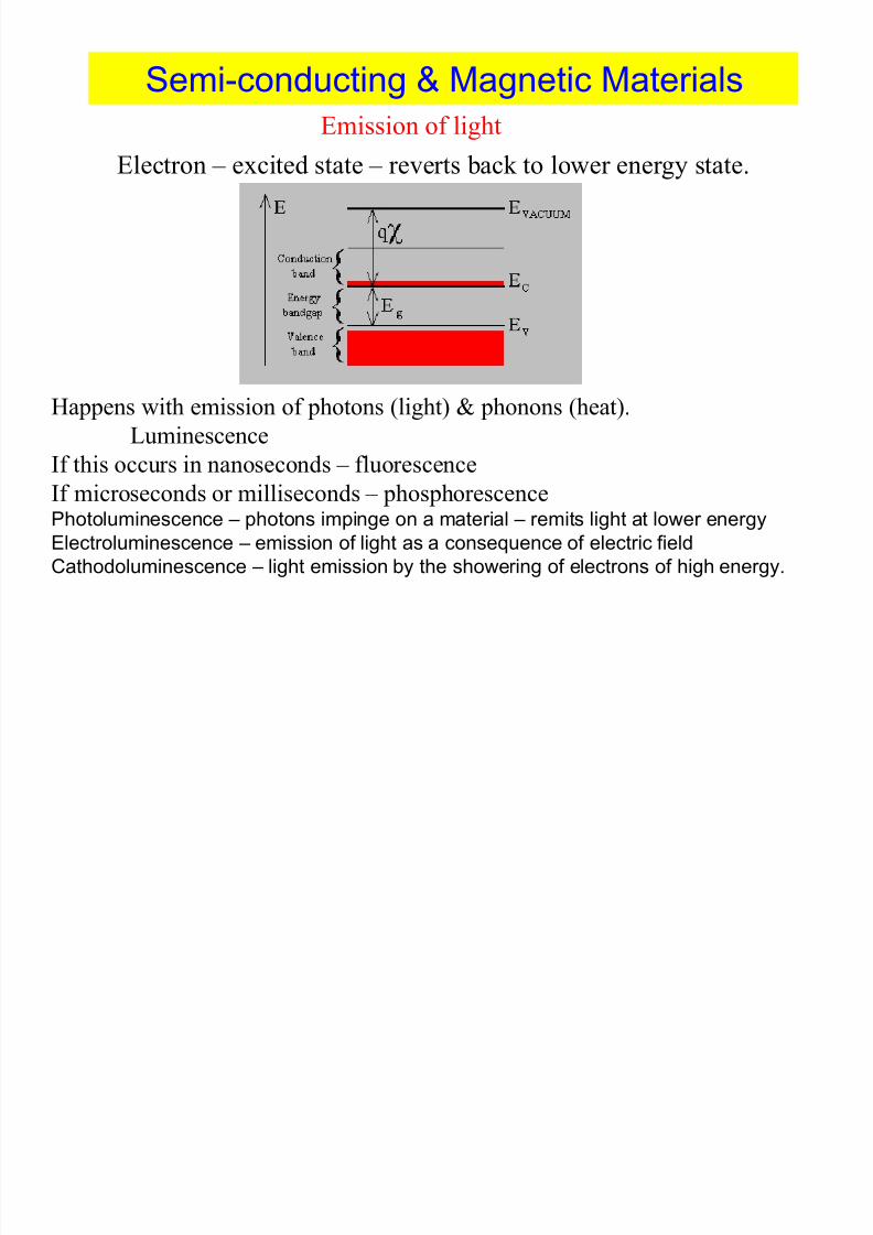
Semi-conducting & Magnetic Materials
Emission of light
Electron – excited state – reverts back to lower energy state.
Happens with emission of photons (light) & phonons (heat).
Luminescence
If this occurs in nanoseconds – fluorescenceIf microseconds or milliseconds – phosphorescencePhotoluminescence – photons impinge on a material – remits light at lower energy
Electroluminescence – emission of light as a consequence of electric field
Cathodoluminescence – light emission by the showering of electrons of high energy.
8/2/2019 Semi Conducting & Magnetic Materials Week 3 Feb 7 2012
http://slidepdf.com/reader/full/semi-conducting-magnetic-materials-week-3-feb-7-2012 3/75
Semi-conducting & Magnetic Materials
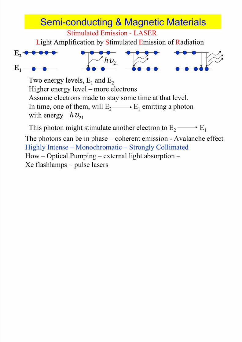
Stimulated Emission - LASER Light Amplification by Stimulated Emission of R adiation
E1
E2
21
υ h
Two energy levels, E1 and E2
Higher energy level – more electrons
Assume electrons made to stay some time at that level.In time, one of them, will E2 E1 emitting a photon
with energy 21υ h
This photon might stimulate another electron to E2 E1
The photons can be in phase – coherent emission - Avalanche effect
Highly Intense – Monochromatic – Strongly Collimated
How – Optical Pumping – external light absorption –
Xe flashlamps – pulse lasers

8/2/2019 Semi Conducting & Magnetic Materials Week 3 Feb 7 2012
http://slidepdf.com/reader/full/semi-conducting-magnetic-materials-week-3-feb-7-2012 4/75
Semi-conducting & Magnetic Materials
Stimulated Emission - LASER
Device current ~ 5 mA at ~ 3V
Input power ~ 15 mW,
η 33%-95% (L.D.)Power density ~ 300-600 W/cm2
Sunlight intensity ? ~100 mW/cm2
2 major Designs for Laser Diodes
8/2/2019 Semi Conducting & Magnetic Materials Week 3 Feb 7 2012
http://slidepdf.com/reader/full/semi-conducting-magnetic-materials-week-3-feb-7-2012 5/75
Semi-conducting & Magnetic Materials
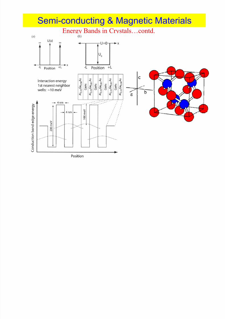
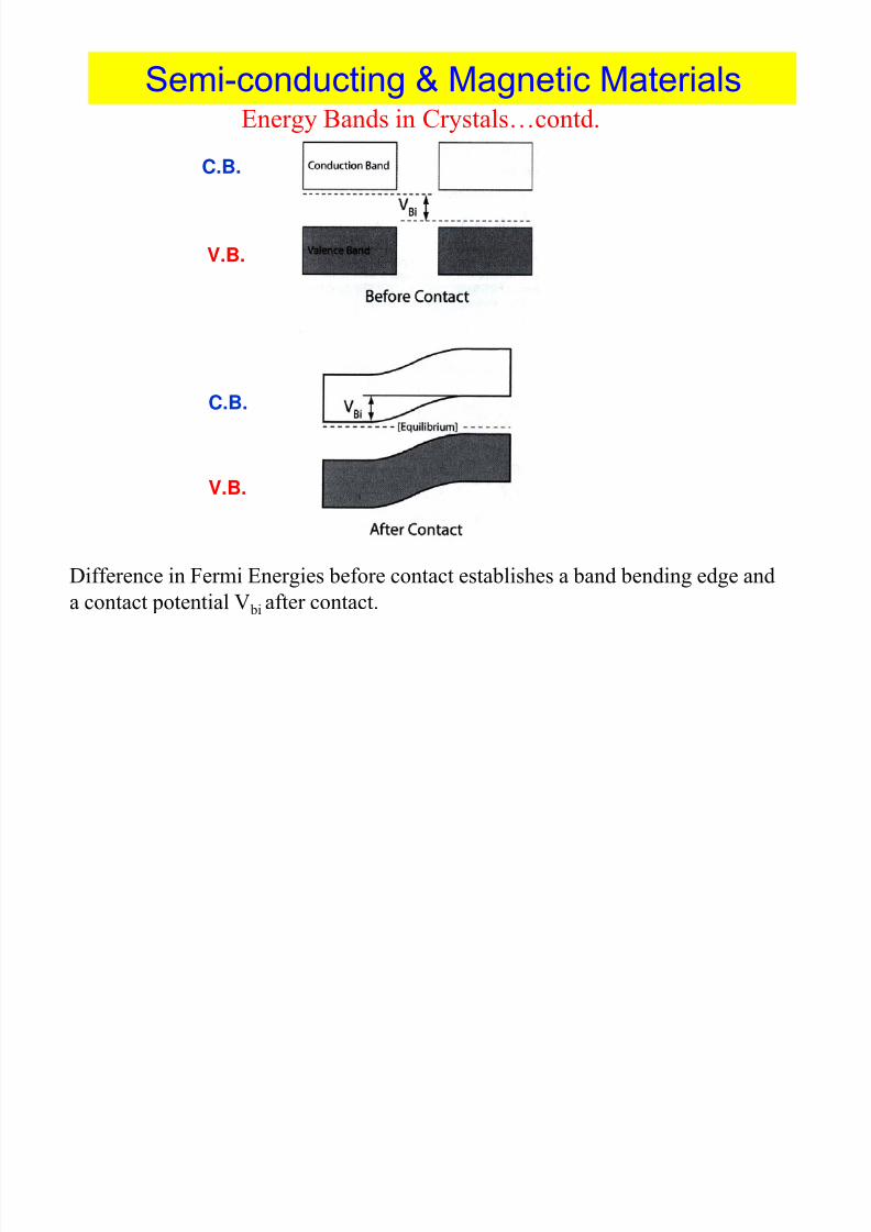
Energy Bands in Crystals…contd.
8/2/2019 Semi Conducting & Magnetic Materials Week 3 Feb 7 2012
http://slidepdf.com/reader/full/semi-conducting-magnetic-materials-week-3-feb-7-2012 6/75
Semi-conducting & Magnetic Materials
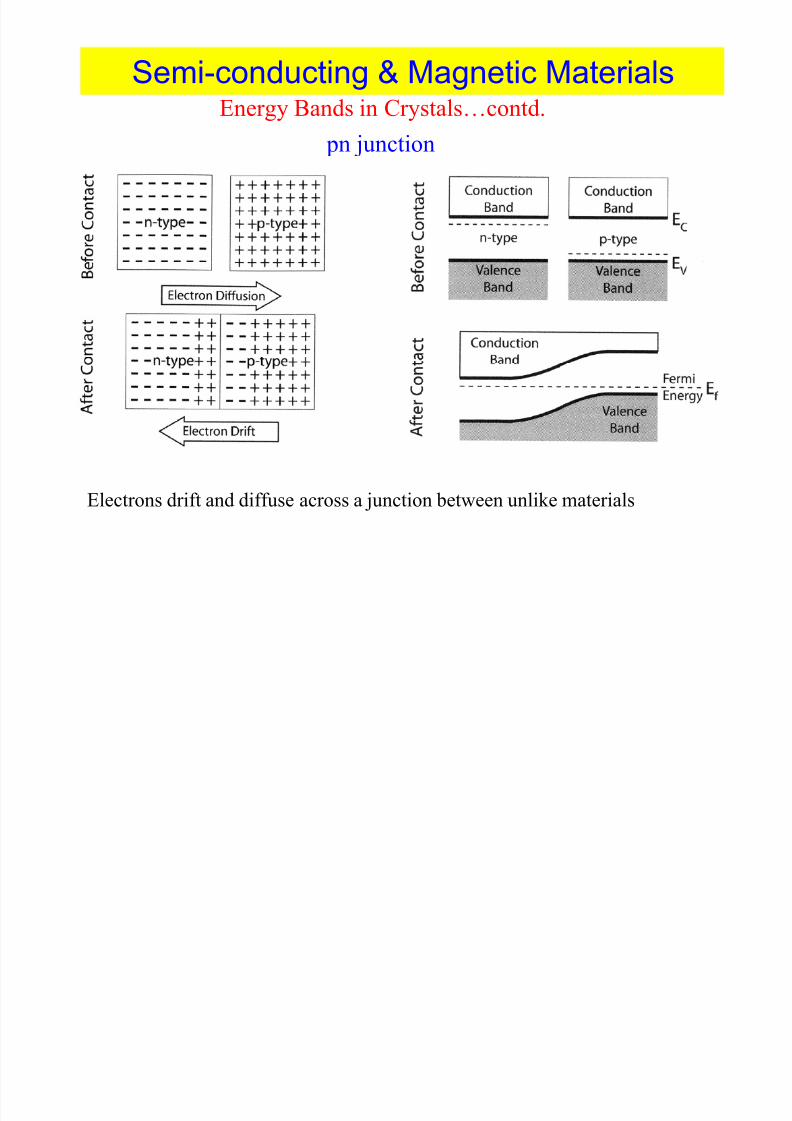
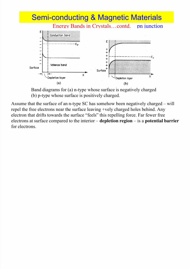
Energy Bands in Crystals…contd. pn junction
Electrons drift and diffuse across a junction between unlike materials
8/2/2019 Semi Conducting & Magnetic Materials Week 3 Feb 7 2012
http://slidepdf.com/reader/full/semi-conducting-magnetic-materials-week-3-feb-7-2012 7/75
Semi-conducting & Magnetic Materials
Energy Bands in Crystals…contd. pn junction
V.B.
V.B.
C.B.
C.B.
Difference in Fermi Energies before contact establishes a band bending edge and
a contact potential V bi after contact.
8/2/2019 Semi Conducting & Magnetic Materials Week 3 Feb 7 2012
http://slidepdf.com/reader/full/semi-conducting-magnetic-materials-week-3-feb-7-2012 8/75
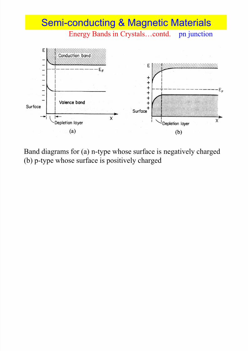
Semi-conducting & Magnetic Materials
Energy Bands in Crystals…contd. pn junction
Band diagrams for (a) n-type whose surface is negatively charged
(b) p-type whose surface is positively charged.
Assume that the surface of an n-type SC has somehow been negatively charged – willrepel the free electrons near the surface leaving +vely charged holes behind. Any
electron that drifts towards the surface “feels” this repelling force. Far fewer free
electrons at surface compared to the interior – depletion region – is a potential barrier
for electrons.
8/2/2019 Semi Conducting & Magnetic Materials Week 3 Feb 7 2012
http://slidepdf.com/reader/full/semi-conducting-magnetic-materials-week-3-feb-7-2012 9/75
Semi-conducting & Magnetic Materials
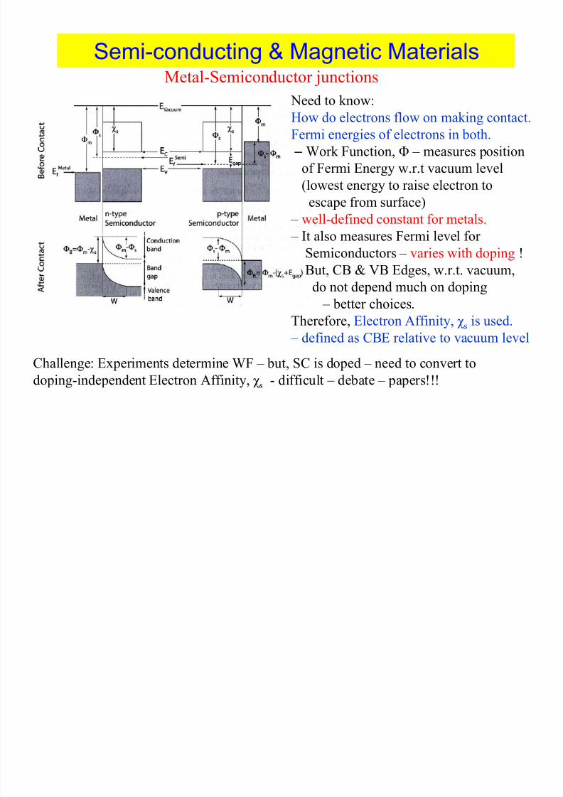
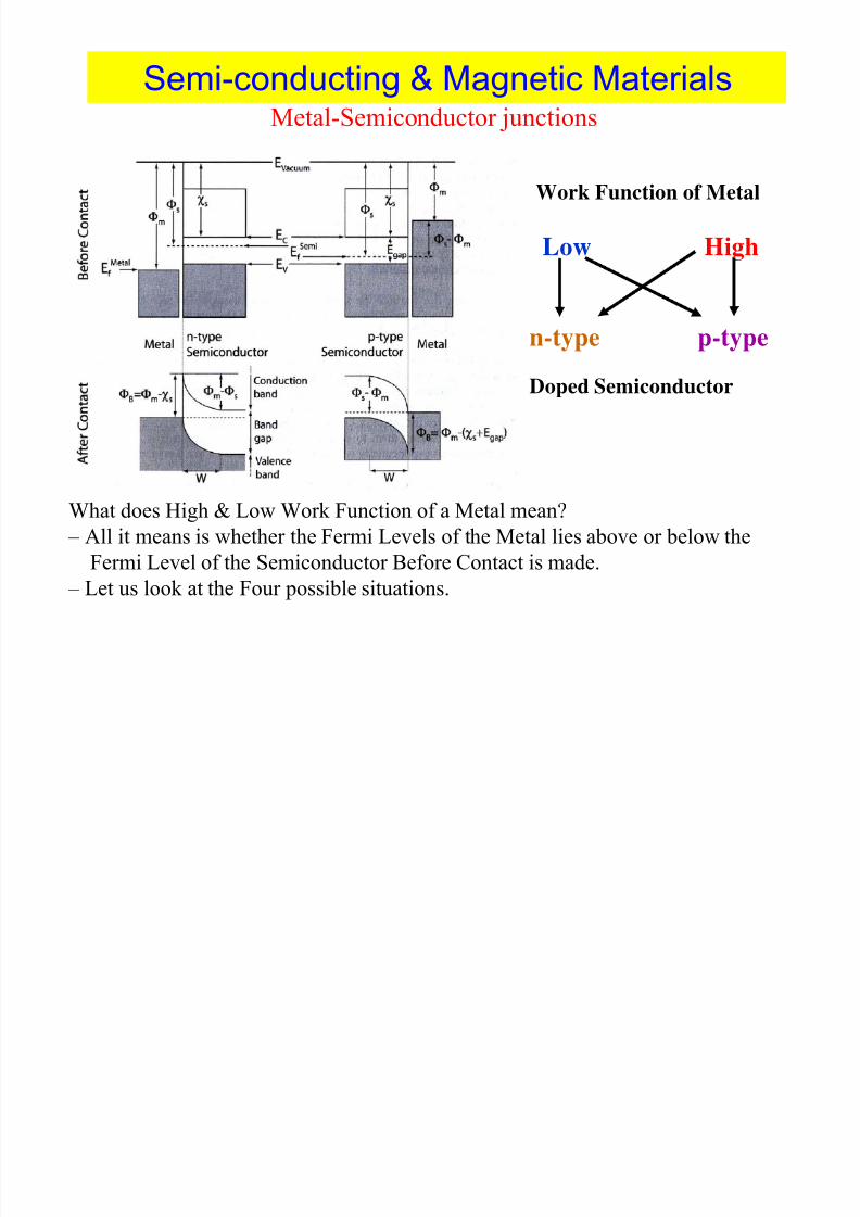
Metal-Semiconductor junctions Need to know:
How do electrons flow on making contact.
Fermi energies of electrons in both.
– Work Function, Φ – measures positionof Fermi Energy w.r.t vacuum level
(lowest energy to raise electron to
escape from surface)
– well-defined constant for metals.
– It also measures Fermi level for
Semiconductors – varies with doping !
But, CB & VB Edges, w.r.t. vacuum,
do not depend much on doping
– better choices.Therefore, Electron Affinity, χ s is used.
– defined as CBE relative to vacuum level
Challenge: Experiments determine WF – but, SC is doped – need to convert to
doping-independent Electron Affinity, χ s - difficult – debate – papers!!!
8/2/2019 Semi Conducting & Magnetic Materials Week 3 Feb 7 2012
http://slidepdf.com/reader/full/semi-conducting-magnetic-materials-week-3-feb-7-2012 10/75
Semi-conducting & Magnetic Materials
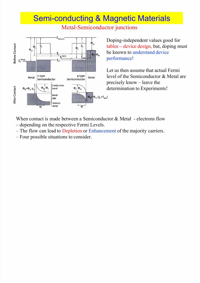
Metal-Semiconductor junctions
Doping-independent values good for
tables – device design, but, doping must
be known to understand device performance!
Let us then assume that actual Fermi
level of the Semiconductor & Metal are
precisely know – leave thedetermination to Experiments!
When contact is made between a Semiconductor & Metal - electrons flow
– depending on the respective Fermi Levels.
– The flow can lead to Depletion or Enhancement of the majority carriers.
– Four possible situations to consider.
8/2/2019 Semi Conducting & Magnetic Materials Week 3 Feb 7 2012
http://slidepdf.com/reader/full/semi-conducting-magnetic-materials-week-3-feb-7-2012 11/75
Semi-conducting & Magnetic Materials
Metal-Semiconductor junctions
Work Function of Metal
What does High & Low Work Function of a Metal mean?
– All it means is whether the Fermi Levels of the Metal lies above or below the
Fermi Level of the Semiconductor Before Contact is made.
– Let us look at the Four possible situations.
Doped Semiconductor
Low High
n-type p-type
8/2/2019 Semi Conducting & Magnetic Materials Week 3 Feb 7 2012
http://slidepdf.com/reader/full/semi-conducting-magnetic-materials-week-3-feb-7-2012 12/75
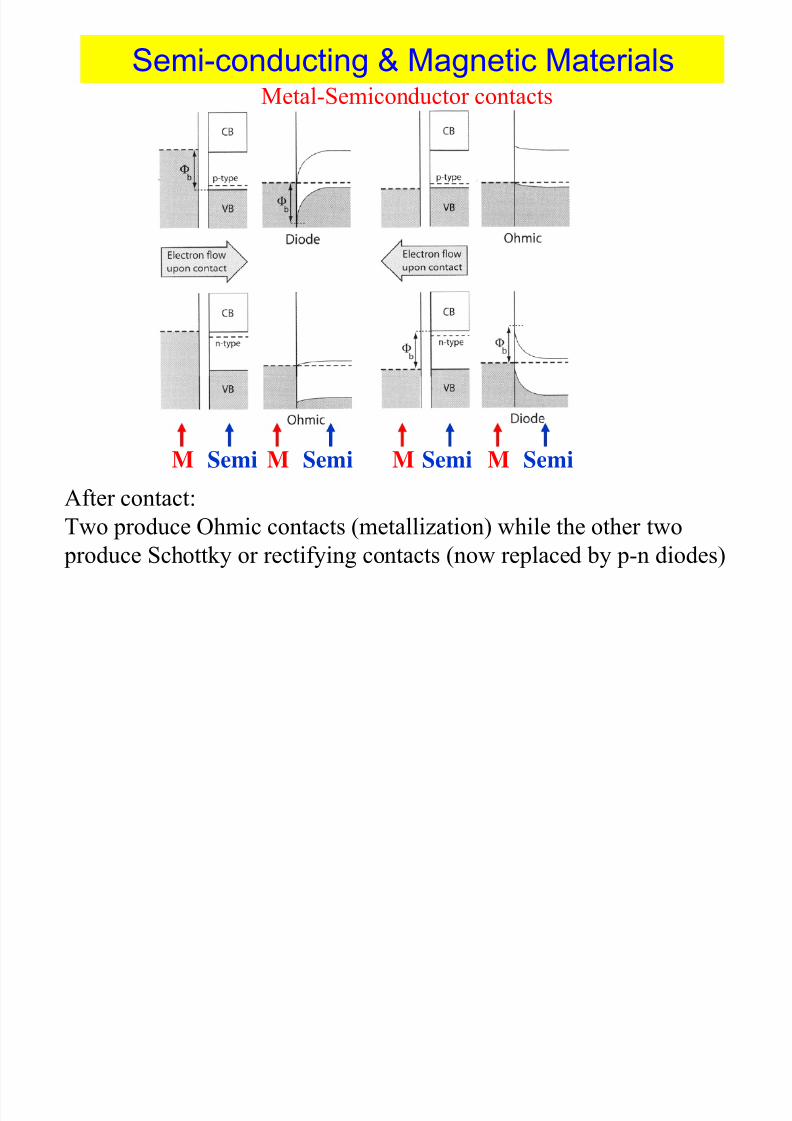
Semi-conducting & Magnetic MaterialsMetal-Semiconductor contacts
After contact:
Two produce Ohmic contacts (metallization) while the other two produce Schottky or rectifying contacts (now replaced by p-n diodes)
M Semi Semi Semi SemiMMM

8/2/2019 Semi Conducting & Magnetic Materials Week 3 Feb 7 2012
http://slidepdf.com/reader/full/semi-conducting-magnetic-materials-week-3-feb-7-2012 13/75
Semi-conducting & Magnetic MaterialsMetal-Semiconductor contacts
Electron Flow Into n-type semiconductor or Out of p-type – Increases Majority carrier
concentration of the semiconductor - increases conductivity of the Semiconductor near
the junction - Ohmic contacts (metallization). Electrons flow from Metal into SC
Difficult to find correct metals with appropriate WF for Wide-Band GapSemiconductors
M Semi Semi Semi SemiMMM
I
V
Ohm’s Law
Ohmic contacts (metallization).
8/2/2019 Semi Conducting & Magnetic Materials Week 3 Feb 7 2012
http://slidepdf.com/reader/full/semi-conducting-magnetic-materials-week-3-feb-7-2012 14/75
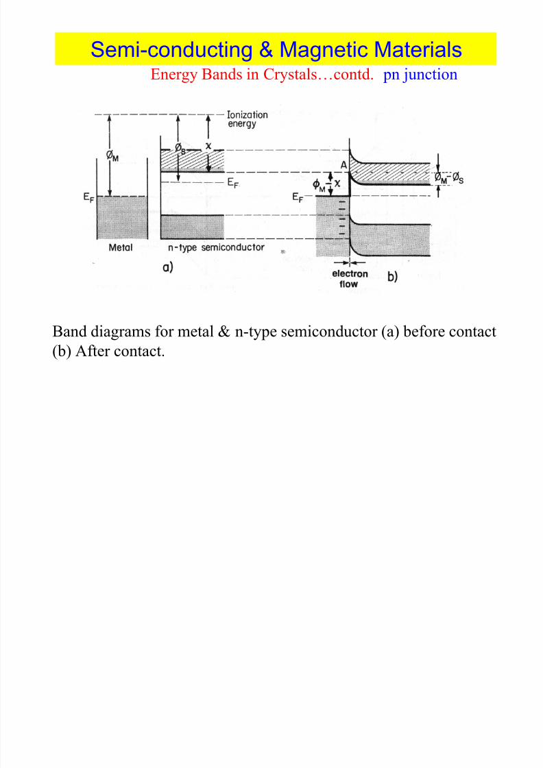
Semi-conducting & Magnetic Materials
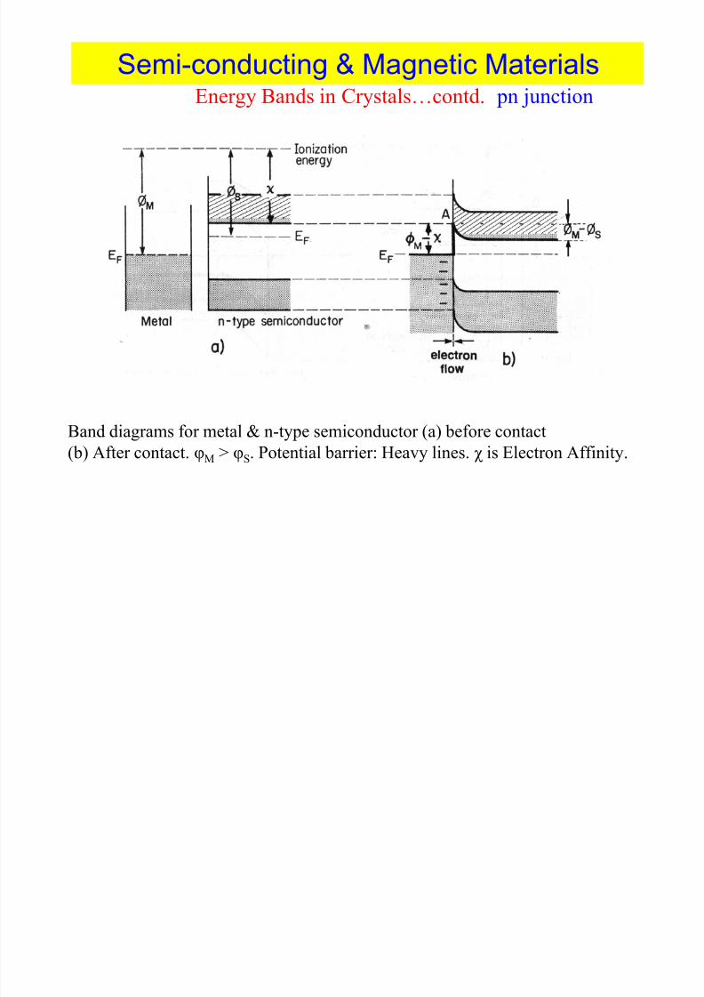
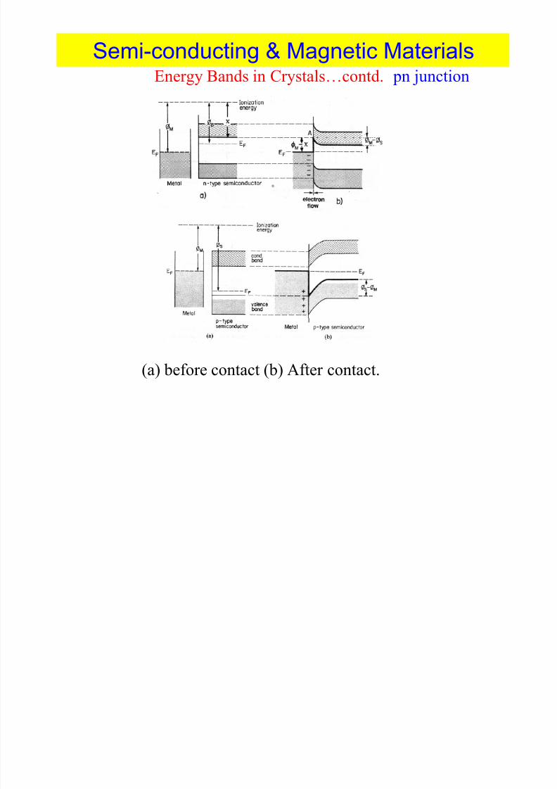
Energy Bands in Crystals…contd. pn junction
Band diagrams for metal & n-type semiconductor (a) before contact
(b) After contact. φM > φS. Potential barrier: Heavy lines. χ is Electron Affinity.

8/2/2019 Semi Conducting & Magnetic Materials Week 3 Feb 7 2012
http://slidepdf.com/reader/full/semi-conducting-magnetic-materials-week-3-feb-7-2012 15/75
Semi-conducting & Magnetic MaterialsMetal-Semiconductor contacts
Electron Flow: When charge flowing Into the semiconductor is opposite sign as the
majority carriers type, the majority carriers are depleted near the junction forming a
resistive depletion layer.
- An applied bias voltage appears across this relatively insulating depleted region – induces current flow.
M Semi Semi Semi SemiMMM

8/2/2019 Semi Conducting & Magnetic Materials Week 3 Feb 7 2012
http://slidepdf.com/reader/full/semi-conducting-magnetic-materials-week-3-feb-7-2012 16/75
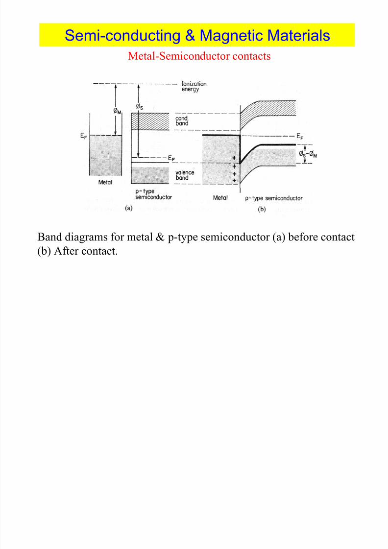
Semi-conducting & Magnetic Materials
Band diagrams for metal & p-type semiconductor (a) before contact
(b) After contact. φM < φS.
Metal-Semiconductor contacts
8/2/2019 Semi Conducting & Magnetic Materials Week 3 Feb 7 2012
http://slidepdf.com/reader/full/semi-conducting-magnetic-materials-week-3-feb-7-2012 17/75
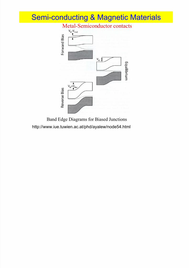
Semi-conducting & Magnetic Materials
Metal-Semiconductor contacts
Band Edge Diagrams for Biased Junctions
http://www.iue.tuwien.ac.at/phd/ayalew/node54.html
8/2/2019 Semi Conducting & Magnetic Materials Week 3 Feb 7 2012
http://slidepdf.com/reader/full/semi-conducting-magnetic-materials-week-3-feb-7-2012 18/75
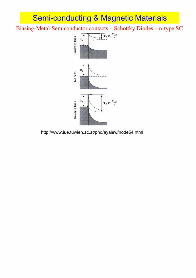
Semi-conducting & Magnetic Materials
Biasing-Metal-Semiconductor contacts – Schottky Diodes – n-type SC
http://www.iue.tuwien.ac.at/phd/ayalew/node54.html
8/2/2019 Semi Conducting & Magnetic Materials Week 3 Feb 7 2012
http://slidepdf.com/reader/full/semi-conducting-magnetic-materials-week-3-feb-7-2012 19/75
Semi-conducting & Magnetic Materials
Energy Bands in Crystals…contd. pn junction
Band diagrams for (a) n-type whose surface is negatively charged
(b) p-type whose surface is positively charged
8/2/2019 Semi Conducting & Magnetic Materials Week 3 Feb 7 2012
http://slidepdf.com/reader/full/semi-conducting-magnetic-materials-week-3-feb-7-2012 20/75
Semi-conducting & Magnetic Materials
Energy Bands in Crystals…contd. pn junction
Band diagrams for metal & n-type semiconductor (a) before contact
(b) After contact.
8/2/2019 Semi Conducting & Magnetic Materials Week 3 Feb 7 2012
http://slidepdf.com/reader/full/semi-conducting-magnetic-materials-week-3-feb-7-2012 21/75
Semi-conducting & Magnetic Materials
Band diagrams for metal & p-type semiconductor (a) before contact
(b) After contact.
Metal-Semiconductor contacts
8/2/2019 Semi Conducting & Magnetic Materials Week 3 Feb 7 2012
http://slidepdf.com/reader/full/semi-conducting-magnetic-materials-week-3-feb-7-2012 22/75
Semi-conducting & Magnetic Materials
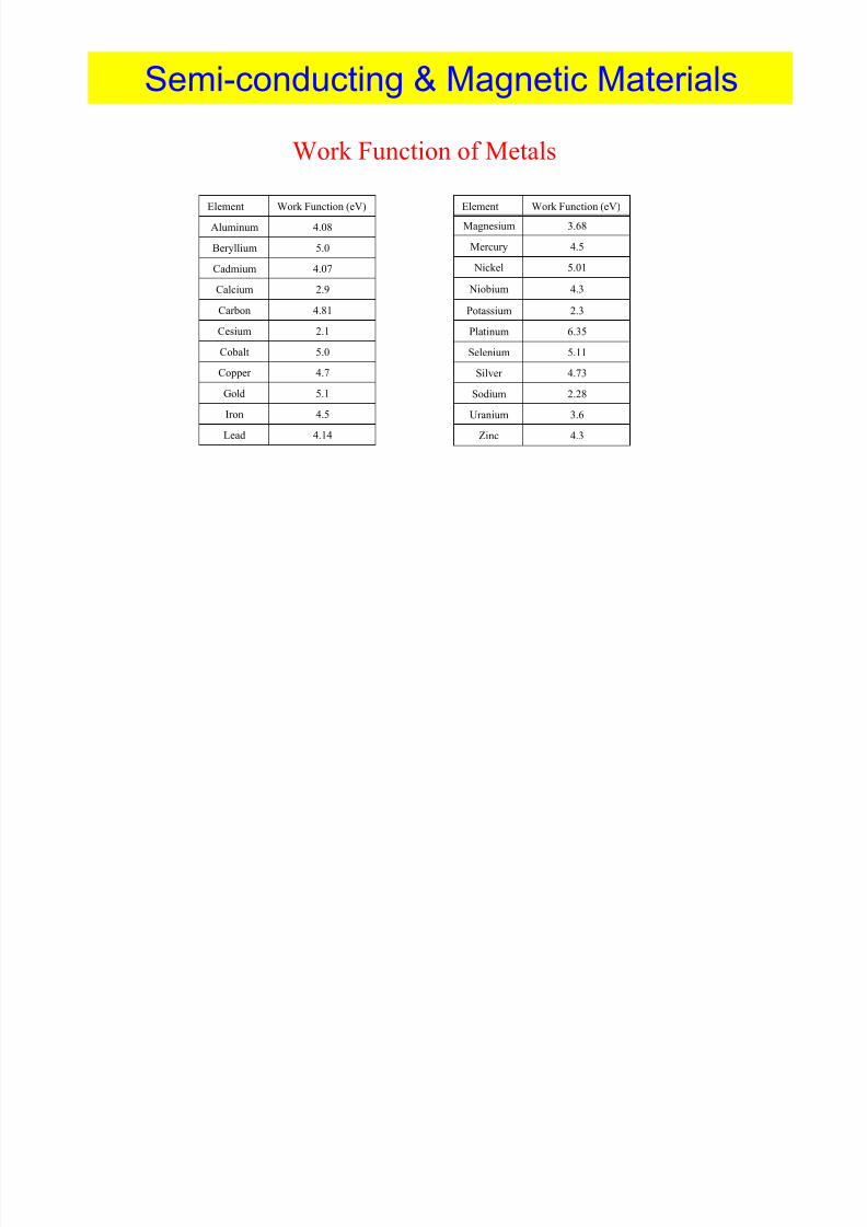
Work Function of Metals
4.14Lead
4.5Iron
5.1Gold
4.7Copper 5.0Cobalt
2.1Cesium
4.81Carbon
2.9Calcium
4.07Cadmium
5.0Beryllium
4.08Aluminum
Work Function (eV)Element
4.3Zinc
3.6Uranium
2.28Sodium
4.73Silver
5.11Selenium
6.35Platinum
2.3Potassium
4.3 Niobium
5.01 Nickel
4.5Mercury
3.68Magnesium
Work Function (eV)Element
8/2/2019 Semi Conducting & Magnetic Materials Week 3 Feb 7 2012
http://slidepdf.com/reader/full/semi-conducting-magnetic-materials-week-3-feb-7-2012 23/75
Semi-conducting & Magnetic Materials
Energy Bands in Crystals…contd. pn junction
(a) before contact (b) After contact.
8/2/2019 Semi Conducting & Magnetic Materials Week 3 Feb 7 2012
http://slidepdf.com/reader/full/semi-conducting-magnetic-materials-week-3-feb-7-2012 24/75
Semi-conducting & Magnetic Materials
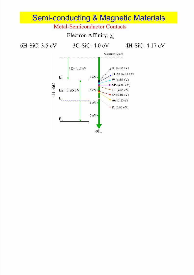
Metal-Semiconductor ContactsElectron Affinity, χ s
6H-SiC: 3.5 eV 3C-SiC: 4.0 eV 4H-SiC: 4.17 eV

8/2/2019 Semi Conducting & Magnetic Materials Week 3 Feb 7 2012
http://slidepdf.com/reader/full/semi-conducting-magnetic-materials-week-3-feb-7-2012 25/75
Semi-conducting & Magnetic Materials
Metal-Semiconductor ContactsElectron Affinity, χ s
6H-SiC: 3.5 eV 3C-SiC: 4.0 eV 4H-SiC: 4.17 eV
Assignment:
Find appropriate metal contact
to form
(a) Ohmic contacts and
(b) Schottky contacts
on n-type and p-type
6H-SiC
3C-SiC4H-SiC
Provide calculations to justify
the selection.
Due: Feb 12, 2009
8/2/2019 Semi Conducting & Magnetic Materials Week 3 Feb 7 2012
http://slidepdf.com/reader/full/semi-conducting-magnetic-materials-week-3-feb-7-2012 26/75
Semi-conducting & Magnetic Materials
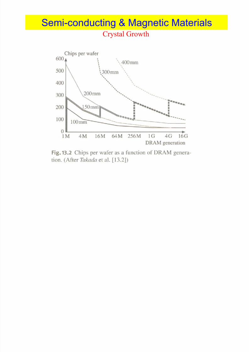
Crystal Growth

8/2/2019 Semi Conducting & Magnetic Materials Week 3 Feb 7 2012
http://slidepdf.com/reader/full/semi-conducting-magnetic-materials-week-3-feb-7-2012 27/75
Semi-conducting & Magnetic Materials
Crystal Growth
8/2/2019 Semi Conducting & Magnetic Materials Week 3 Feb 7 2012
http://slidepdf.com/reader/full/semi-conducting-magnetic-materials-week-3-feb-7-2012 28/75
Semi-conducting & Magnetic Materials
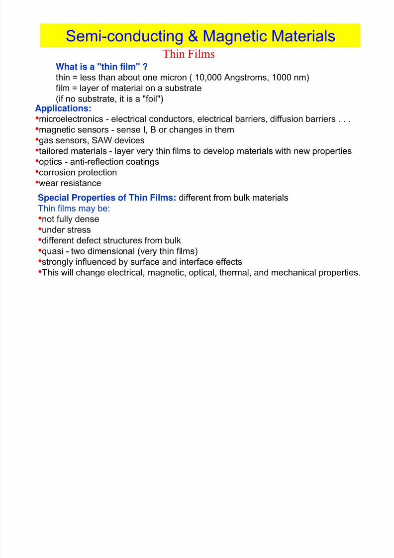
Thin FilmsWhat is a "thin film" ?thin = less than about one micron ( 10,000 Angstroms, 1000 nm)
film = layer of material on a substrate
(if no substrate, it is a "foil")
Applications:•microelectronics - electrical conductors, electrical barriers, diffusion barriers . . .
•magnetic sensors - sense I, B or changes in them
•gas sensors, SAW devices
•tailored materials - layer very thin films to develop materials with new properties
•optics - anti-reflection coatings•corrosion protection
•wear resistance
Special Properties of Thin Films: different from bulk materials
Thin films may be:
•not fully dense•under stress
•different defect structures from bulk
•quasi - two dimensional (very thin films)
•strongly influenced by surface and interface effects
•This will change electrical, magnetic, optical, thermal, and mechanical properties.
8/2/2019 Semi Conducting & Magnetic Materials Week 3 Feb 7 2012
http://slidepdf.com/reader/full/semi-conducting-magnetic-materials-week-3-feb-7-2012 29/75
Semi-conducting & Magnetic Materials
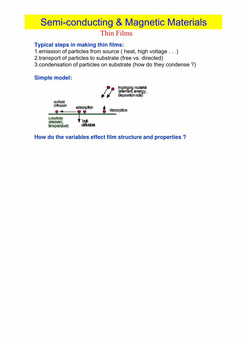
Thin FilmsTypical steps in making thin films:1.emission of particles from source ( heat, high voltage . . .)
2.transport of particles to substrate (free vs. directed)
3.condensation of particles on substrate (how do they condense ?)
Simple model:
How do the variables effect film structure and properties ?
8/2/2019 Semi Conducting & Magnetic Materials Week 3 Feb 7 2012
http://slidepdf.com/reader/full/semi-conducting-magnetic-materials-week-3-feb-7-2012 30/75
Semi-conducting & Magnetic Materials
Thin FilmsWhat physics is in all this ?
thermodynamics and kinetics
phase transition - gas condenses to solid
nucleation
growth kinetics activated processes
• desorption
• diffusion
allowed processes and allowed phases
solid state physics crystallography
defects
bonding
electricity and magnetism
optics conductivity - resistivity
magnetic properties
mechanics
stresses in films
friction and wear
8/2/2019 Semi Conducting & Magnetic Materials Week 3 Feb 7 2012
http://slidepdf.com/reader/full/semi-conducting-magnetic-materials-week-3-feb-7-2012 31/75
8/2/2019 Semi Conducting & Magnetic Materials Week 3 Feb 7 2012
http://slidepdf.com/reader/full/semi-conducting-magnetic-materials-week-3-feb-7-2012 32/75
Semi-conducting & Magnetic Materials
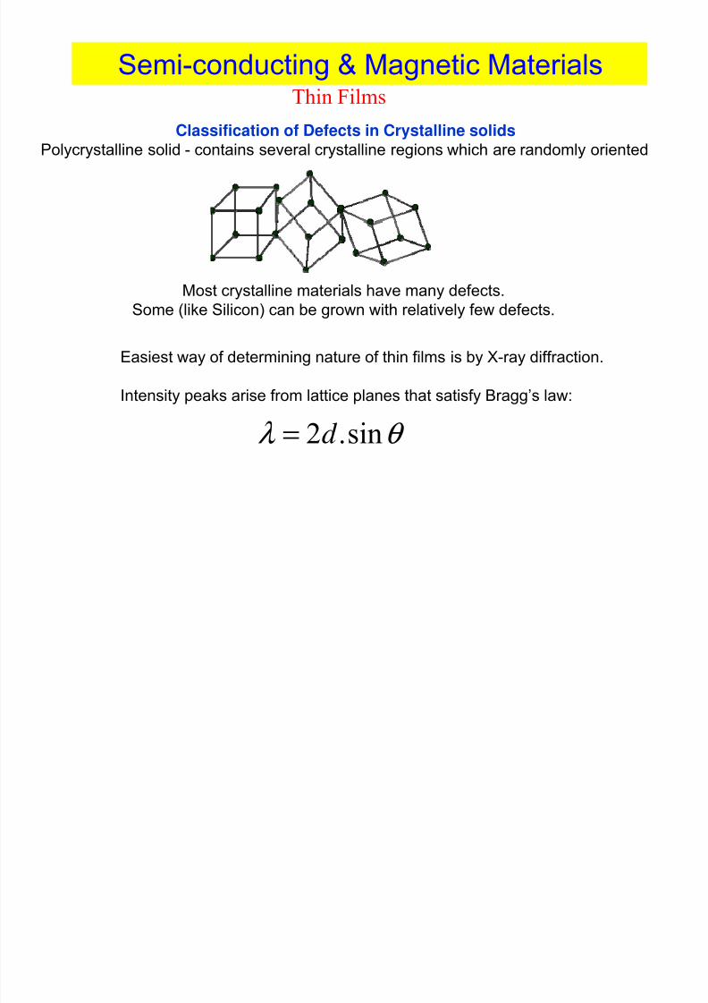
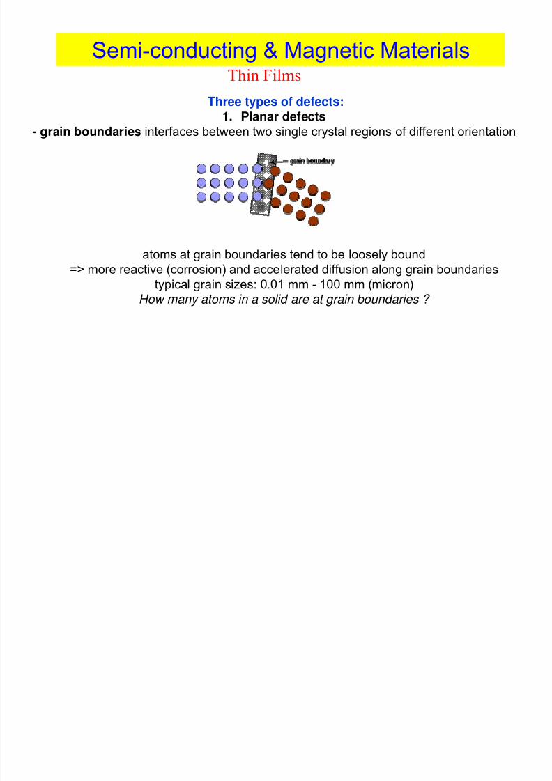
Thin FilmsThree types of defects:
1. Planar defects
- grain boundaries interfaces between two single crystal regions of different orientation
atoms at grain boundaries tend to be loosely bound
=> more reactive (corrosion) and accelerated diffusion along grain boundaries
typical grain sizes: 0.01 mm - 100 mm (micron)
How many atoms in a solid are at grain boundaries ?
8/2/2019 Semi Conducting & Magnetic Materials Week 3 Feb 7 2012
http://slidepdf.com/reader/full/semi-conducting-magnetic-materials-week-3-feb-7-2012 33/75
Semi-conducting & Magnetic Materials
Thin Films
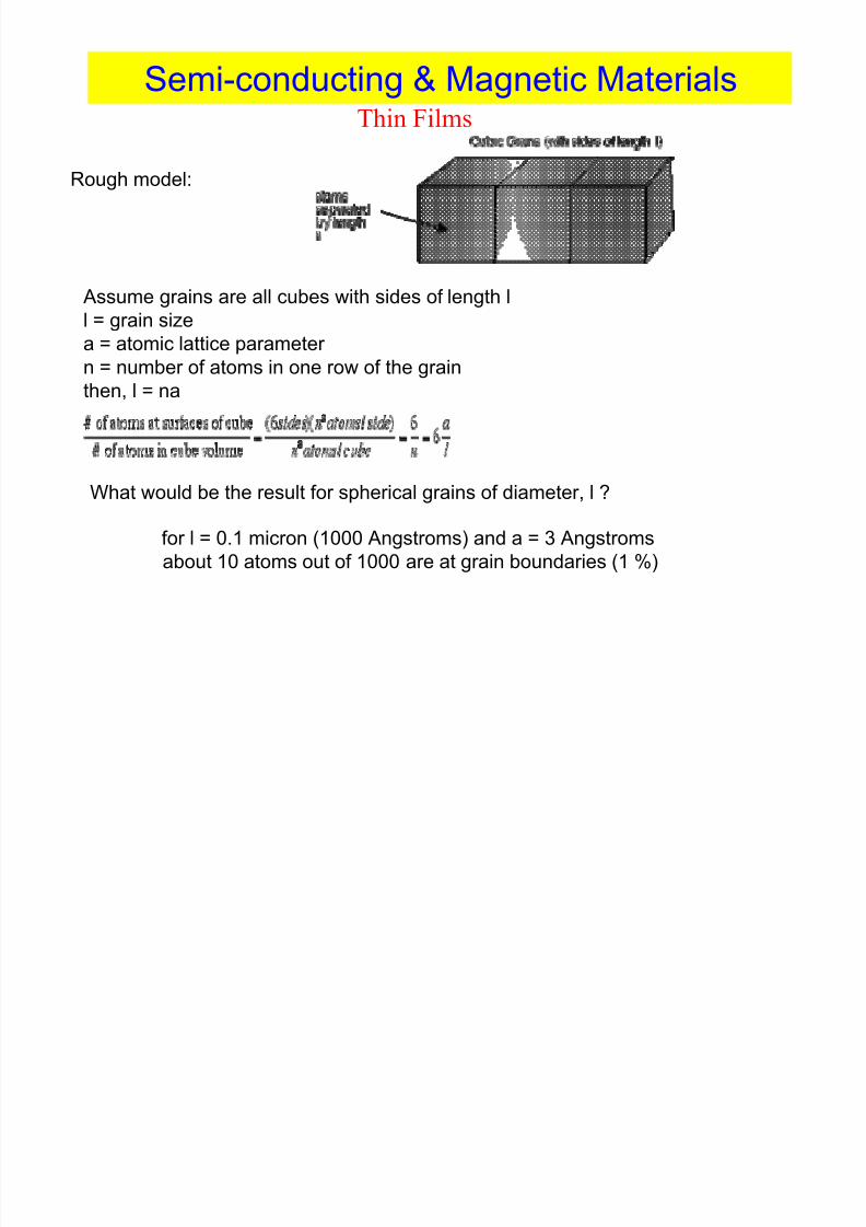
Rough model:
Assume grains are all cubes with sides of length l
l = grain size
a = atomic lattice parameter
n = number of atoms in one row of the grain
then, l = na
What would be the result for spherical grains of diameter, l ?
for l = 0.1 micron (1000 Angstroms) and a = 3 Angstroms
about 10 atoms out of 1000 are at grain boundaries (1 %)
8/2/2019 Semi Conducting & Magnetic Materials Week 3 Feb 7 2012
http://slidepdf.com/reader/full/semi-conducting-magnetic-materials-week-3-feb-7-2012 34/75
Semi-conducting & Magnetic Materials
Thin Films Number of grain boundaries in film (grain size) depends
on deposition rate and substrate temperature.
generally:
lower T => smaller grains => many boundaries
higher T => larger grains => fewer boundaries
grain size is often proportional to film thickness
(thinner films tend to have smaller grains)
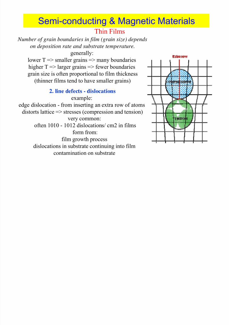
2. line defects - dislocations
example:
edge dislocation - from inserting an extra row of atoms
distorts lattice => stresses (compression and tension)
very common:
often 1010 - 1012 dislocations/ cm2 in filmsform from:
film growth process
dislocations in substrate continuing into film
contamination on substrate
8/2/2019 Semi Conducting & Magnetic Materials Week 3 Feb 7 2012
http://slidepdf.com/reader/full/semi-conducting-magnetic-materials-week-3-feb-7-2012 35/75
Semi-conducting & Magnetic Materials
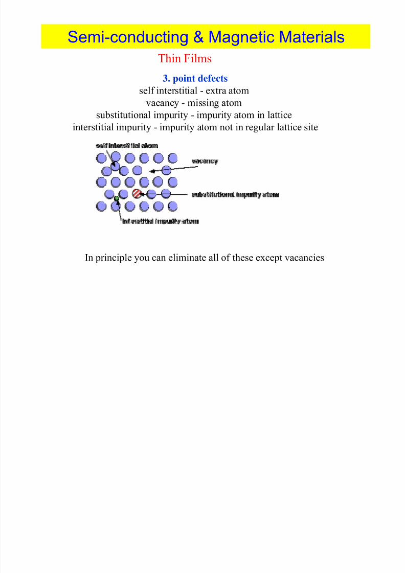
3. point defects
self interstitial - extra atom
vacancy - missing atom
substitutional impurity - impurity atom in latticeinterstitial impurity - impurity atom not in regular lattice site
In principle you can eliminate all of these except vacancies
Thin Films
8/2/2019 Semi Conducting & Magnetic Materials Week 3 Feb 7 2012
http://slidepdf.com/reader/full/semi-conducting-magnetic-materials-week-3-feb-7-2012 36/75
Semi-conducting & Magnetic Materials
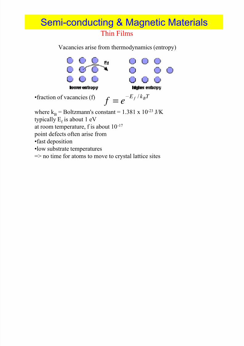
Vacancies arise from thermodynamics (entropy)
•fraction of vacancies (f)
where k B
= Boltzmann's constant = 1.381 x 10⁻²³ J/K
typically Ef is about 1 eV
at room temperature, f is about 10-17
point defects often arise from•fast deposition
•low substrate temperatures
=> no time for atoms to move to crystal lattice sites
T k E B f
e f /−
=
Thin Films
8/2/2019 Semi Conducting & Magnetic Materials Week 3 Feb 7 2012
http://slidepdf.com/reader/full/semi-conducting-magnetic-materials-week-3-feb-7-2012 37/75
Semi-conducting & Magnetic Materials
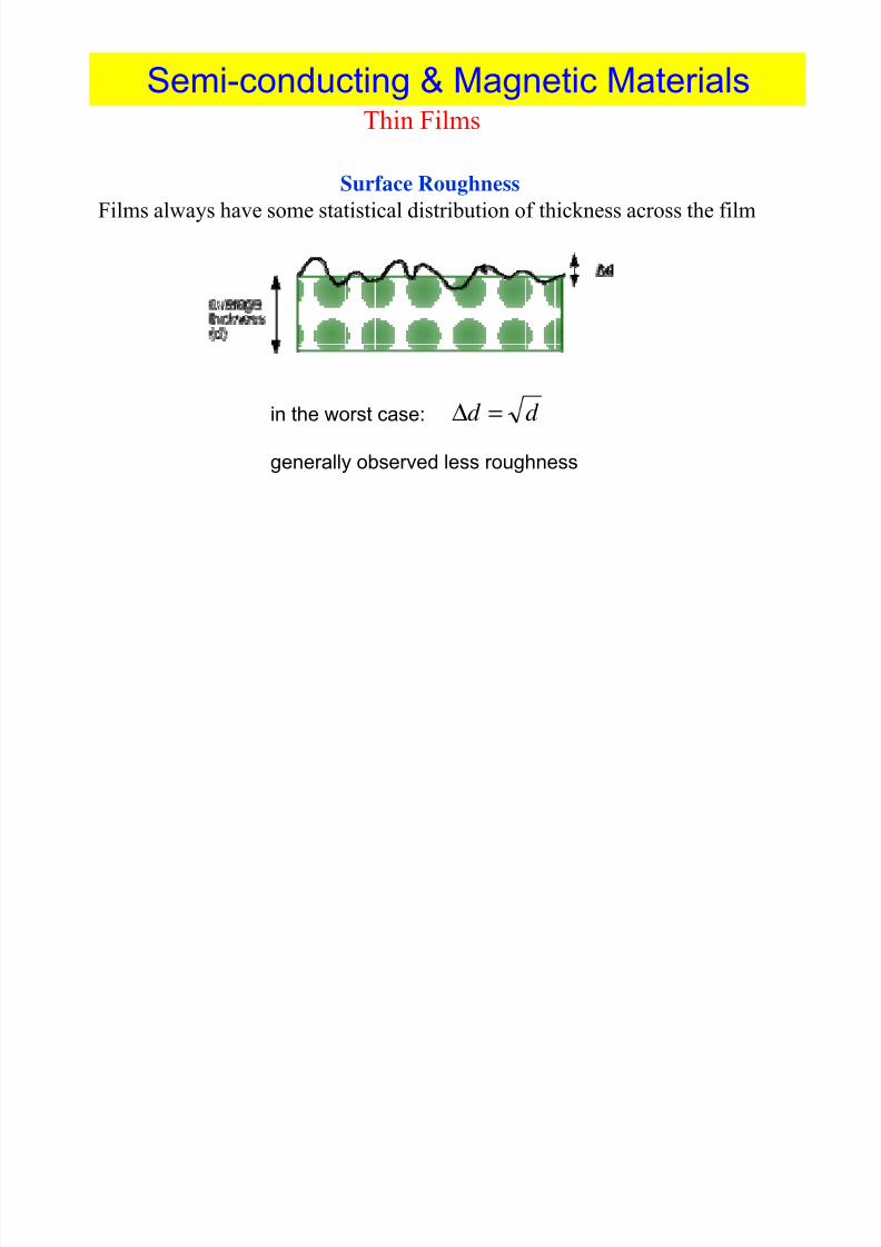
Thin Films
Surface Roughness
Films always have some statistical distribution of thickness across the film
in the worst case:
generally observed less roughness
d d =Δ
8/2/2019 Semi Conducting & Magnetic Materials Week 3 Feb 7 2012
http://slidepdf.com/reader/full/semi-conducting-magnetic-materials-week-3-feb-7-2012 38/75
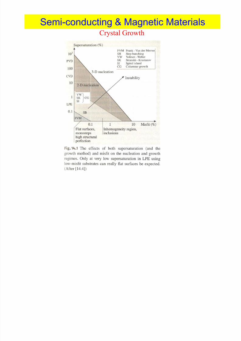
Semi-conducting & Magnetic Materials
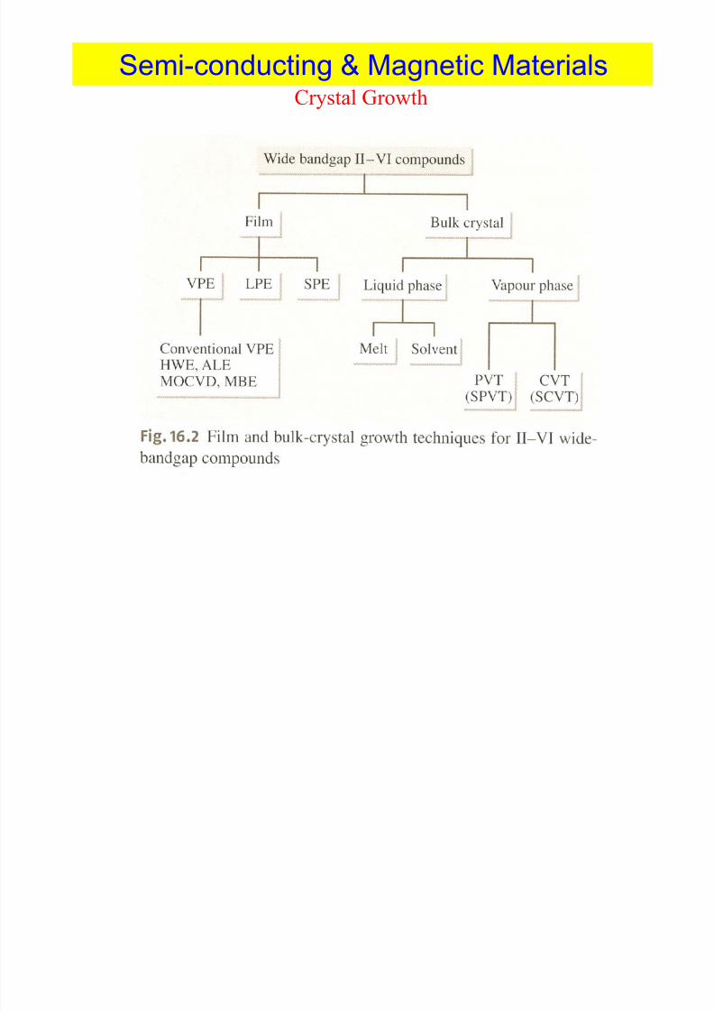
Crystal Growth
8/2/2019 Semi Conducting & Magnetic Materials Week 3 Feb 7 2012
http://slidepdf.com/reader/full/semi-conducting-magnetic-materials-week-3-feb-7-2012 39/75
Semi-conducting & Magnetic Materials
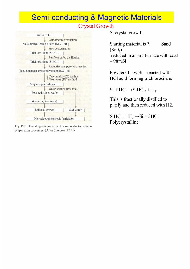
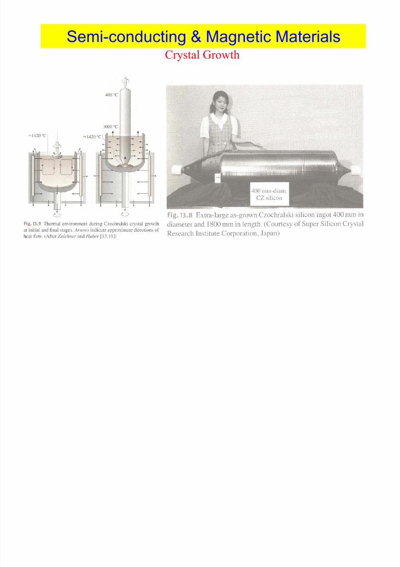
Crystal GrowthSi crystal growth
Starting material is ? Sand
(SiO2) –
reduced in an arc furnace with coal
– 98%Si
Powdered raw Si – reacted with
HCl acid forming trichlorosilane
Si + HCl →SiHCl3 + H2
This is fractionally distilled to
purify and then reduced with H2.
SiHCl3 + H2 →Si + 3HCl
Polycrystalline
8/2/2019 Semi Conducting & Magnetic Materials Week 3 Feb 7 2012
http://slidepdf.com/reader/full/semi-conducting-magnetic-materials-week-3-feb-7-2012 40/75
Semi-conducting & Magnetic Materials
Crystal Growth
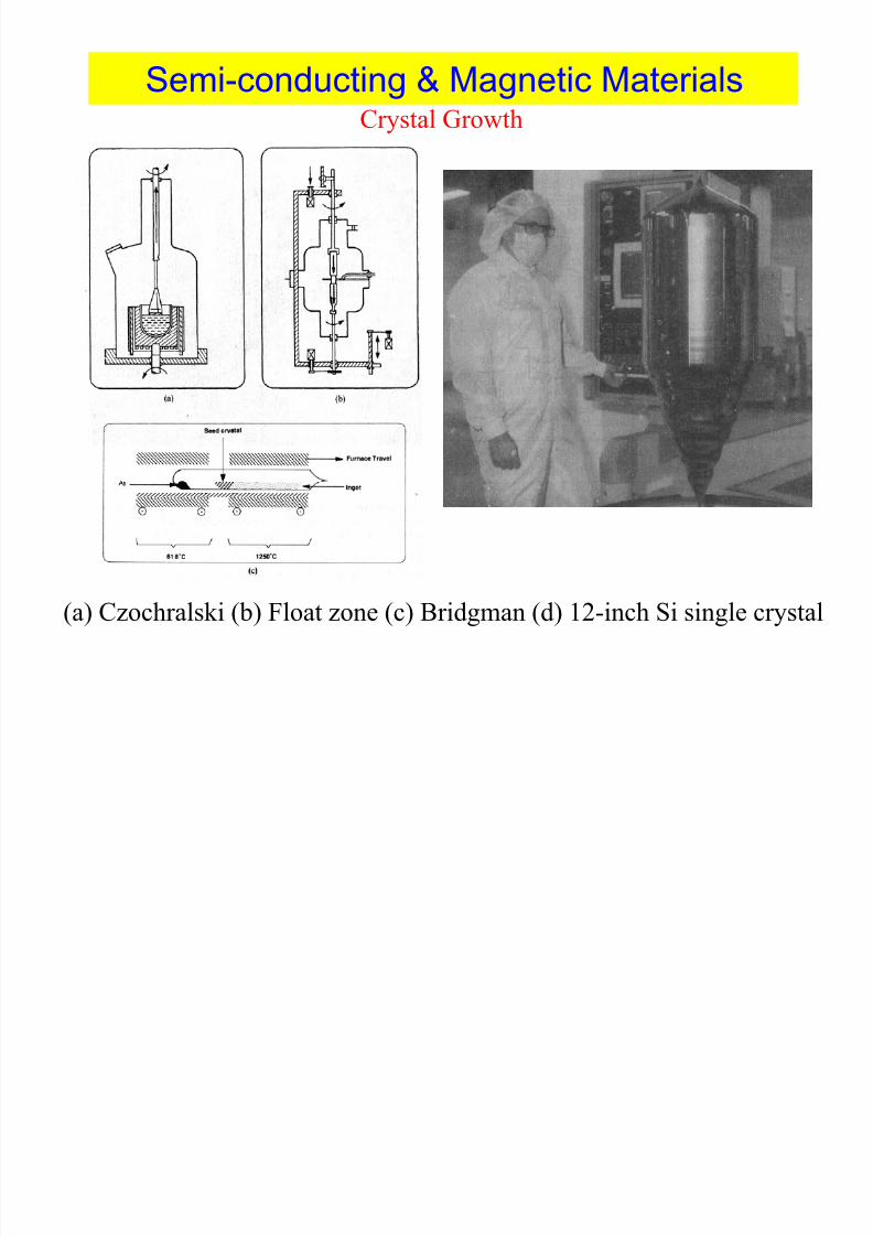
(a) Czochralski (b) Float zone (c) Bridgman (d) 12-inch Si single crystal
8/2/2019 Semi Conducting & Magnetic Materials Week 3 Feb 7 2012
http://slidepdf.com/reader/full/semi-conducting-magnetic-materials-week-3-feb-7-2012 41/75
Semi-conducting & Magnetic Materials
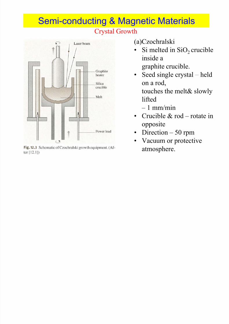
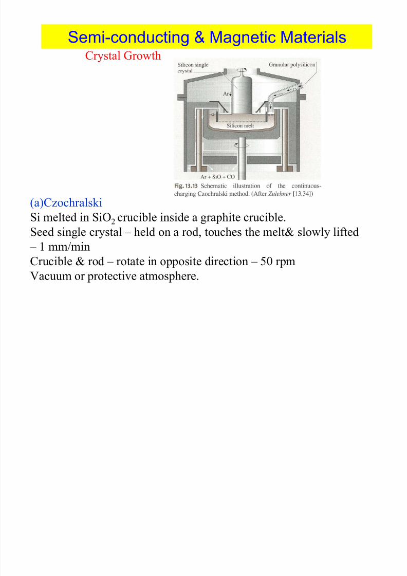
Crystal Growth(a)Czochralski
• Si melted in SiO2 crucible
inside a
graphite crucible.• Seed single crystal – held
on a rod,
touches the melt& slowly
lifted
– 1 mm/min
• Crucible & rod – rotate in
opposite• Direction – 50 rpm
• Vacuum or protective
atmosphere.
S i d ti & M ti M t i l
8/2/2019 Semi Conducting & Magnetic Materials Week 3 Feb 7 2012
http://slidepdf.com/reader/full/semi-conducting-magnetic-materials-week-3-feb-7-2012 42/75
Semi-conducting & Magnetic Materials
Crystal Growth
S i d ti & M ti M t i l
8/2/2019 Semi Conducting & Magnetic Materials Week 3 Feb 7 2012
http://slidepdf.com/reader/full/semi-conducting-magnetic-materials-week-3-feb-7-2012 43/75
Semi-conducting & Magnetic Materials
Crystal Growth
(a)Czochralski
Si melted in SiO2
crucible inside a graphite crucible.
Seed single crystal – held on a rod, touches the melt& slowly lifted
– 1 mm/min
Crucible & rod – rotate in opposite direction – 50 rpm
Vacuum or protective atmosphere.
S i d ti & M ti M t i l
8/2/2019 Semi Conducting & Magnetic Materials Week 3 Feb 7 2012
http://slidepdf.com/reader/full/semi-conducting-magnetic-materials-week-3-feb-7-2012 44/75
Semi-conducting & Magnetic Materials
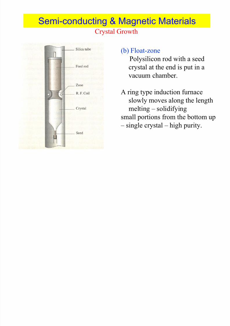
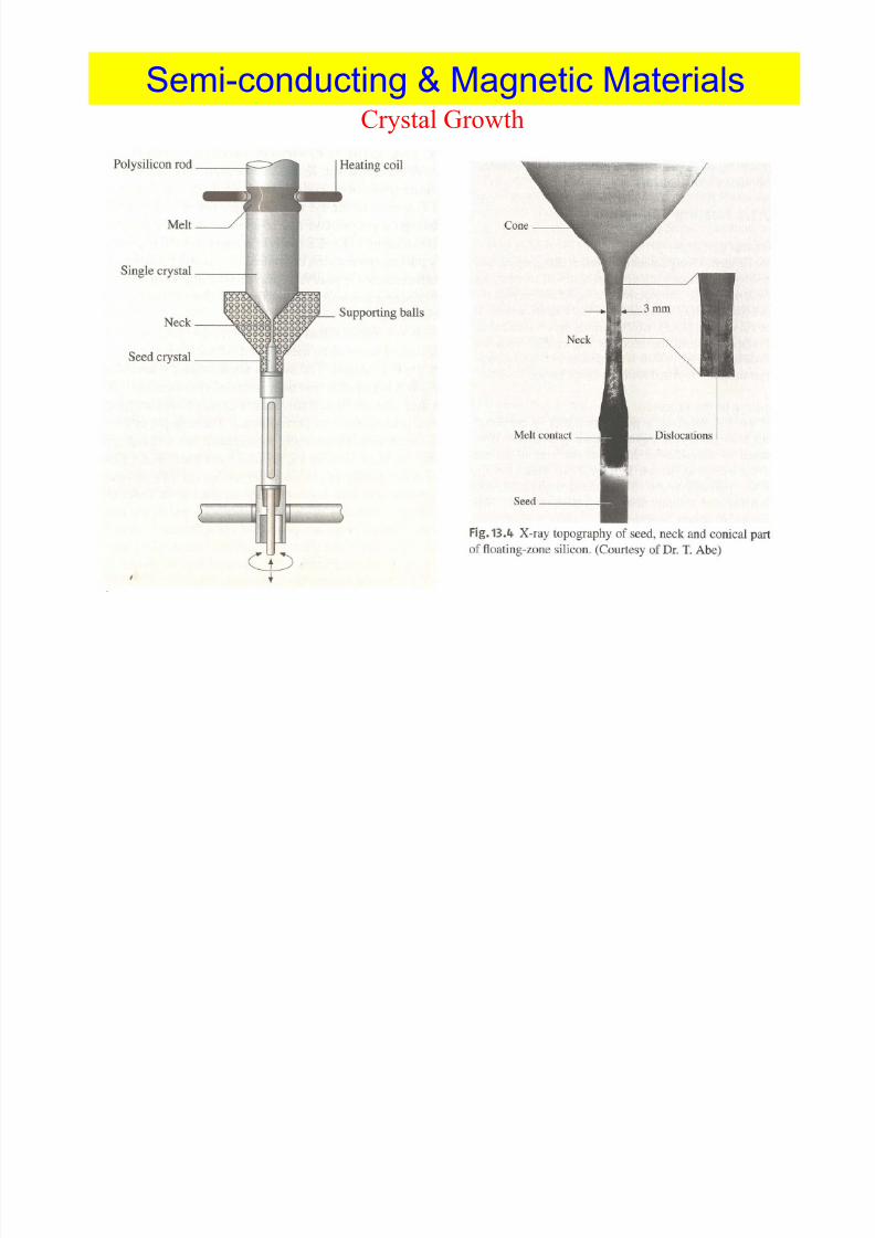
Crystal Growth
(b) Float-zone
Polysilicon rod with a seed
crystal at the end is put in avacuum chamber.
A ring type induction furnace
slowly moves along the length
melting – solidifying
small portions from the bottom up
– single crystal – high purity.
S i d ti & M ti M t i l
8/2/2019 Semi Conducting & Magnetic Materials Week 3 Feb 7 2012
http://slidepdf.com/reader/full/semi-conducting-magnetic-materials-week-3-feb-7-2012 45/75
Semi-conducting & Magnetic Materials
Crystal Growth
Semi conducting & Magnetic Materials
8/2/2019 Semi Conducting & Magnetic Materials Week 3 Feb 7 2012
http://slidepdf.com/reader/full/semi-conducting-magnetic-materials-week-3-feb-7-2012 46/75
Semi-conducting & Magnetic Materials
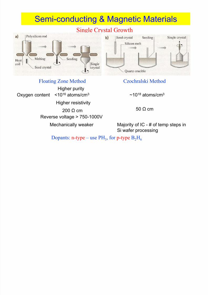
Single Crystal Growth
Floating Zone Method Czochralski Method
Dopants: n-type – use PH3, for p-type B2H6
Higher purity
Oxygen content <1016 atoms/cm3 ~1018 atoms/cm3
Higher resistivity
200 Ω cm 50 Ω cm
Reverse voltage > 750-1000V
Mechanically weaker Majority of IC - # of temp steps in
Si wafer processing
Semi conducting & Magnetic Materials

8/2/2019 Semi Conducting & Magnetic Materials Week 3 Feb 7 2012
http://slidepdf.com/reader/full/semi-conducting-magnetic-materials-week-3-feb-7-2012 47/75
Semi-conducting & Magnetic Materials
Crystal Growth
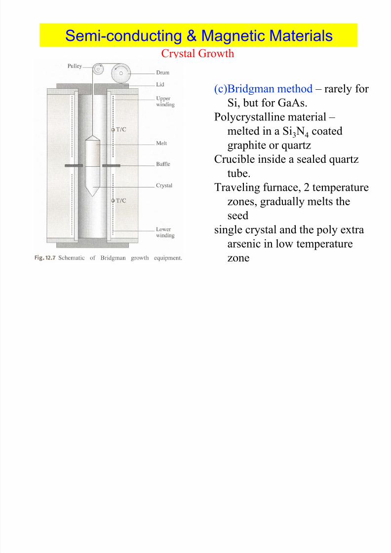
(c)Bridgman method – rarely for Si, but for GaAs.
Polycrystalline material – melted in a Si3 N4 coated graphite or quartzCrucible inside a sealed quartz tube.
Traveling furnace, 2 temperature zones, gradually melts the seed
single crystal and the poly extra arsenic in low temperature zone
Semi conducting & Magnetic Materials
8/2/2019 Semi Conducting & Magnetic Materials Week 3 Feb 7 2012
http://slidepdf.com/reader/full/semi-conducting-magnetic-materials-week-3-feb-7-2012 48/75
Semi-conducting & Magnetic Materials
Crystal Growth
(c)Bridgman method – rarely for
Si, but for GaAs.
Polycrystalline material –
melted in a Si3 N4 coated
graphite or quartz
Crucible inside a sealed quartztube.
Traveling furnace, 2 temperature
zones, gradually melts the
seedsingle crystal and the poly extra
arsenic in low temperature
zone
Semi conducting & Magnetic Materials
8/2/2019 Semi Conducting & Magnetic Materials Week 3 Feb 7 2012
http://slidepdf.com/reader/full/semi-conducting-magnetic-materials-week-3-feb-7-2012 49/75
Semi-conducting & Magnetic Materials
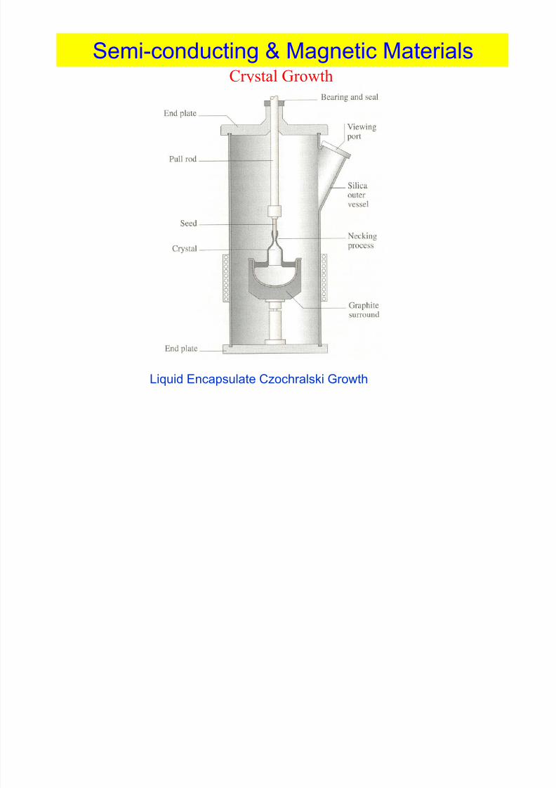
Crystal Growth
Liquid Encapsulate Czochralski Growth
Semi-conducting & Magnetic Materials

8/2/2019 Semi Conducting & Magnetic Materials Week 3 Feb 7 2012
http://slidepdf.com/reader/full/semi-conducting-magnetic-materials-week-3-feb-7-2012 50/75
Semi-conducting & Magnetic Materials
Crystal Growth
Semi-conducting & Magnetic Materials

8/2/2019 Semi Conducting & Magnetic Materials Week 3 Feb 7 2012
http://slidepdf.com/reader/full/semi-conducting-magnetic-materials-week-3-feb-7-2012 51/75
Semi-conducting & Magnetic Materials
Crystal Growth
Semi-conducting & Magnetic Materials
8/2/2019 Semi Conducting & Magnetic Materials Week 3 Feb 7 2012
http://slidepdf.com/reader/full/semi-conducting-magnetic-materials-week-3-feb-7-2012 52/75
Semi conducting & Magnetic Materials
Crystal Growth
Semi-conducting & Magnetic Materials

8/2/2019 Semi Conducting & Magnetic Materials Week 3 Feb 7 2012
http://slidepdf.com/reader/full/semi-conducting-magnetic-materials-week-3-feb-7-2012 53/75
Semi conducting & Magnetic Materials
Crystal Growth
Semi-conducting & Magnetic Materials

8/2/2019 Semi Conducting & Magnetic Materials Week 3 Feb 7 2012
http://slidepdf.com/reader/full/semi-conducting-magnetic-materials-week-3-feb-7-2012 54/75
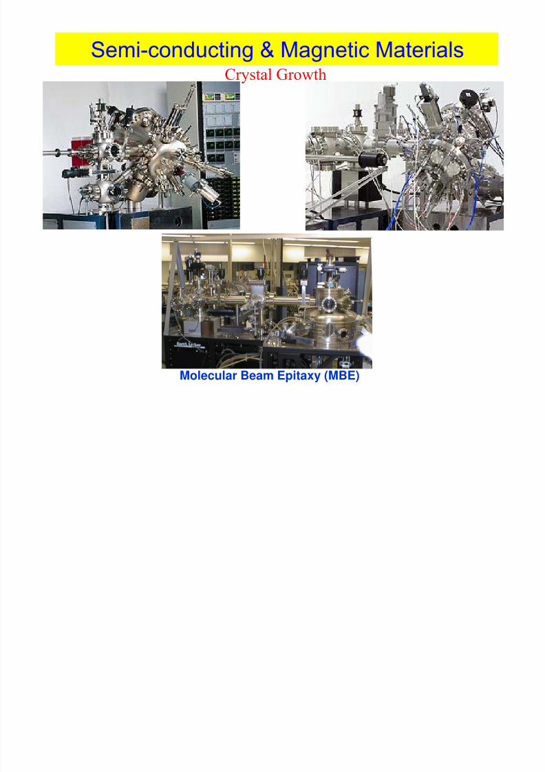
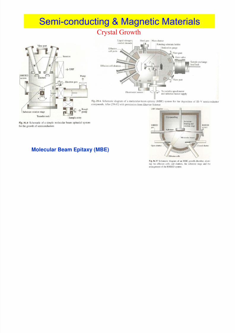
Semi conducting & Magnetic Materials
Thin Film Growth
Molecular Beam Epitaxy (MBE)
Metal-Organic Chemical Vapour Deposition (MOCVD)
Chemical Vapour Deposition (CVD)
Magnetron Sputtering
Pulsed Laser Deposition (PLD)
Ion Beam Deposition (IBD) – amorphous or fine grains?
- LPCVD, APCVD, PECVD
Atomic Layer Deposition (ALD) – amorphous or fine grains?
Single Crystal - Epitaxy
Poly-Crystal
Semi-conducting & Magnetic Materials
8/2/2019 Semi Conducting & Magnetic Materials Week 3 Feb 7 2012
http://slidepdf.com/reader/full/semi-conducting-magnetic-materials-week-3-feb-7-2012 55/75
Semi conducting & Magnetic Materials
Crystal Growth
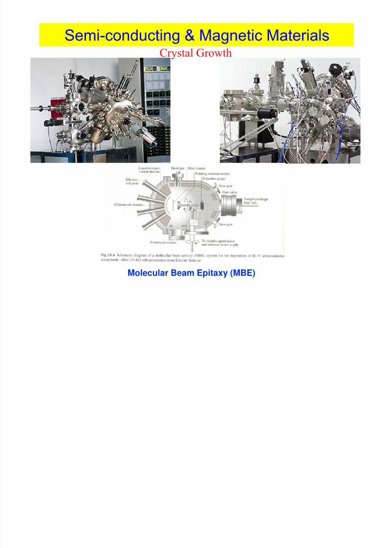
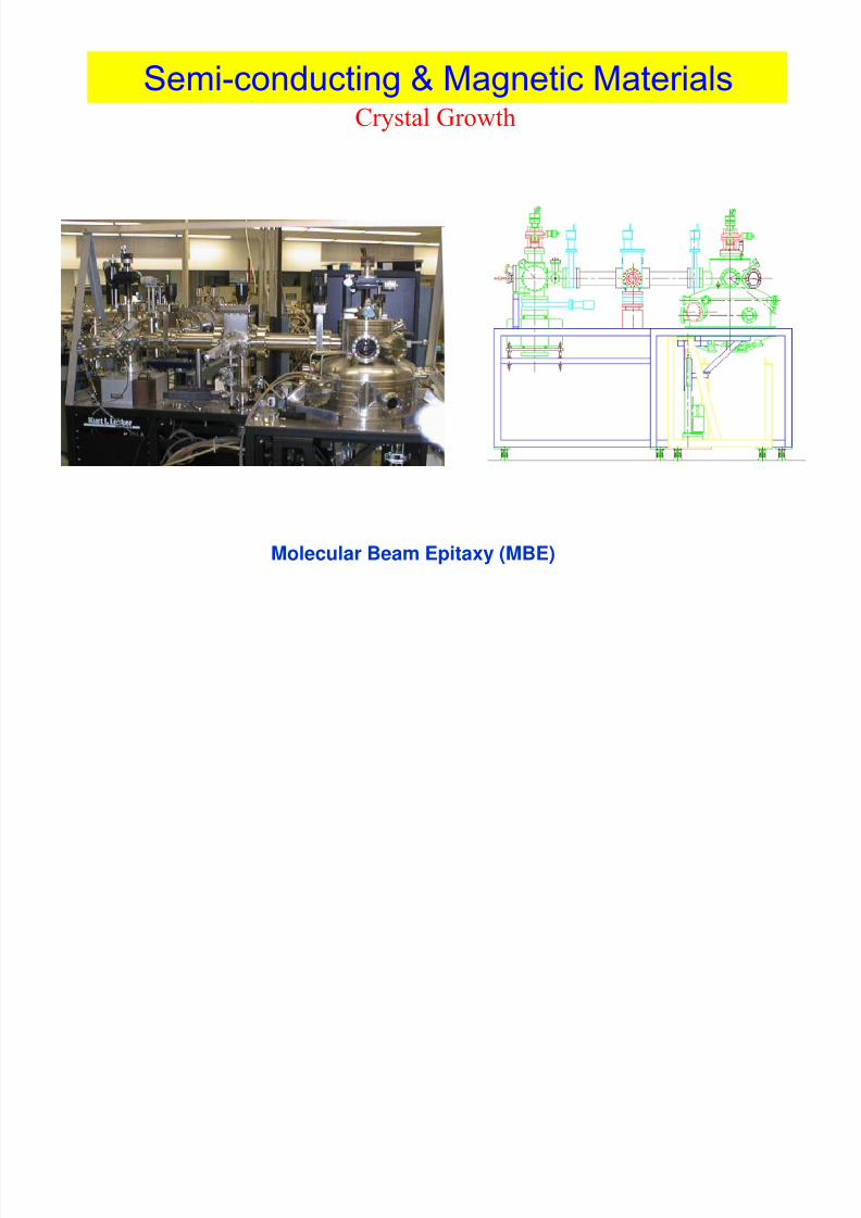
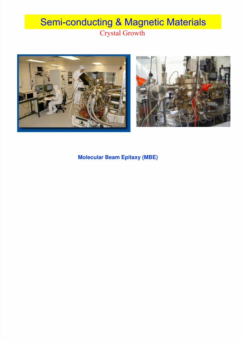
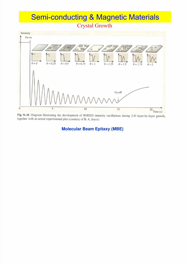
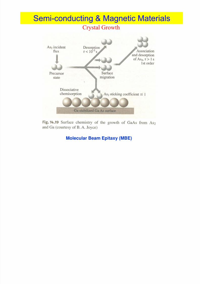
Molecular Beam Epitaxy (MBE)
Semi-conducting & Magnetic Materials
8/2/2019 Semi Conducting & Magnetic Materials Week 3 Feb 7 2012
http://slidepdf.com/reader/full/semi-conducting-magnetic-materials-week-3-feb-7-2012 56/75
Semi conducting & Magnetic MaterialsCrystal Growth
Molecular Beam Epitaxy (MBE)
Semi-conducting & Magnetic Materials

8/2/2019 Semi Conducting & Magnetic Materials Week 3 Feb 7 2012
http://slidepdf.com/reader/full/semi-conducting-magnetic-materials-week-3-feb-7-2012 57/75
g gCrystal Growth
Molecular Beam Epitaxy (MBE)
Semi-conducting & Magnetic Materials
8/2/2019 Semi Conducting & Magnetic Materials Week 3 Feb 7 2012
http://slidepdf.com/reader/full/semi-conducting-magnetic-materials-week-3-feb-7-2012 58/75
g gCrystal Growth
Molecular Beam Epitaxy (MBE)
Semi-conducting & Magnetic Materials
8/2/2019 Semi Conducting & Magnetic Materials Week 3 Feb 7 2012
http://slidepdf.com/reader/full/semi-conducting-magnetic-materials-week-3-feb-7-2012 59/75
g gCrystal Growth
Molecular Beam Epitaxy (MBE)
Semi-conducting & Magnetic Materials
8/2/2019 Semi Conducting & Magnetic Materials Week 3 Feb 7 2012
http://slidepdf.com/reader/full/semi-conducting-magnetic-materials-week-3-feb-7-2012 60/75
g gCrystal Growth
Molecular Beam Epitaxy (MBE)
Semi-conducting & Magnetic Materials
8/2/2019 Semi Conducting & Magnetic Materials Week 3 Feb 7 2012
http://slidepdf.com/reader/full/semi-conducting-magnetic-materials-week-3-feb-7-2012 61/75
Crystal Growth
Molecular Beam Epitaxy (MBE)
Semi-conducting & Magnetic Materials
8/2/2019 Semi Conducting & Magnetic Materials Week 3 Feb 7 2012
http://slidepdf.com/reader/full/semi-conducting-magnetic-materials-week-3-feb-7-2012 62/75
Crystal Growth
Molecular Beam Epitaxy (MBE)
Semi-conducting & Magnetic Materials
8/2/2019 Semi Conducting & Magnetic Materials Week 3 Feb 7 2012
http://slidepdf.com/reader/full/semi-conducting-magnetic-materials-week-3-feb-7-2012 63/75
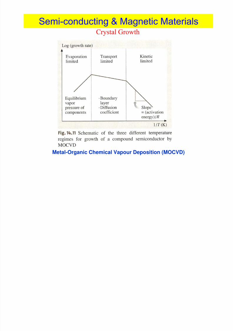
Crystal Growth
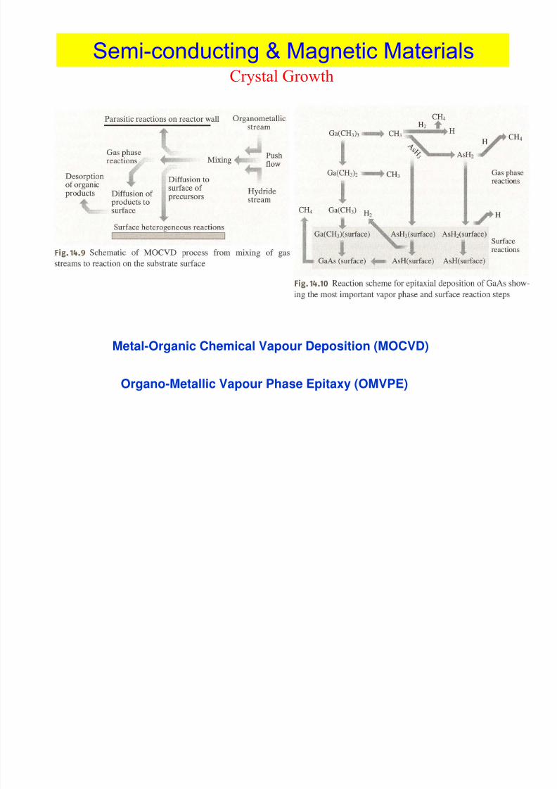
Metal-Organic Chemical Vapour Deposition (MOCVD)
Organo-Metallic Vapour Phase Epitaxy (OMVPE)
Semi-conducting & Magnetic Materials
8/2/2019 Semi Conducting & Magnetic Materials Week 3 Feb 7 2012
http://slidepdf.com/reader/full/semi-conducting-magnetic-materials-week-3-feb-7-2012 64/75
Crystal Growth
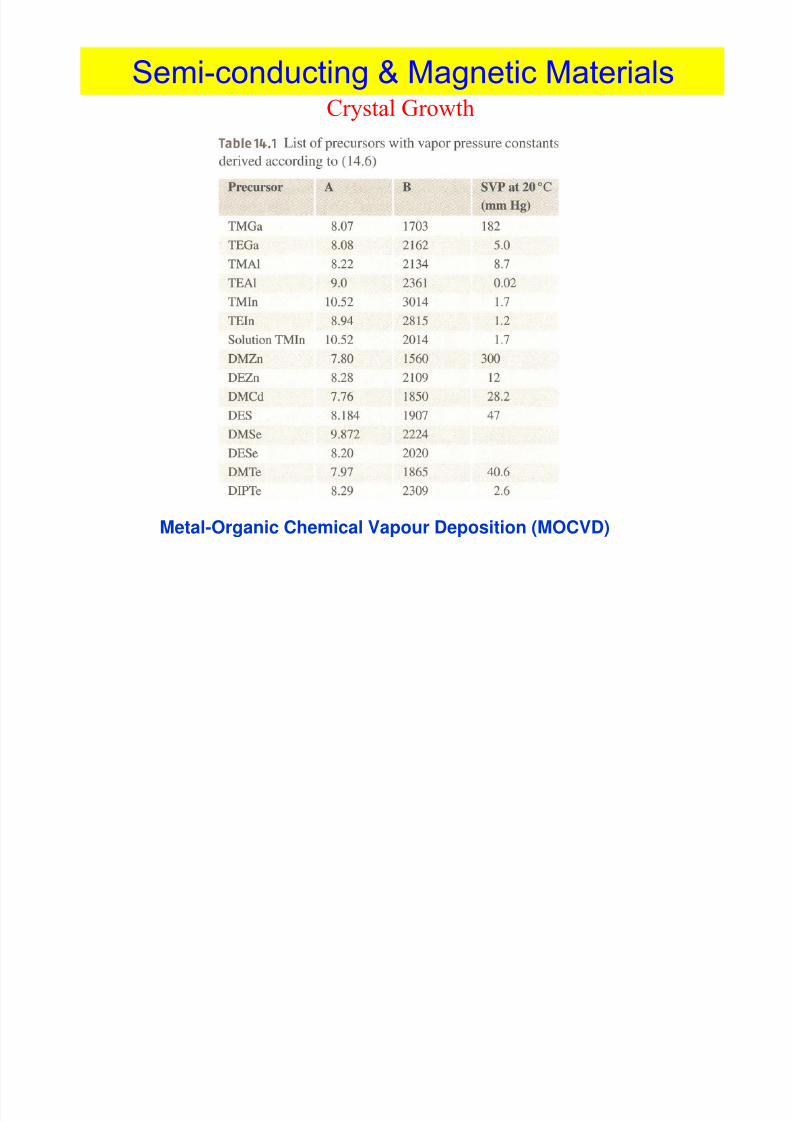
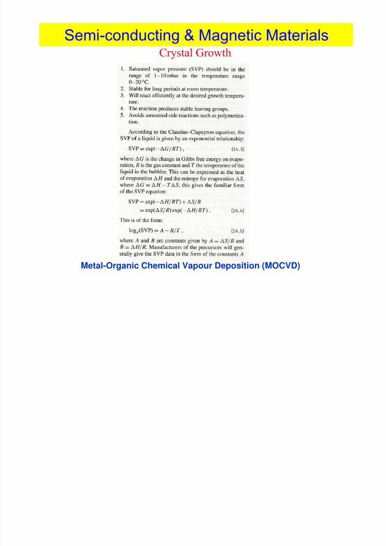
Metal-Organic Chemical Vapour Deposition (MOCVD)
Semi-conducting & Magnetic Materials
8/2/2019 Semi Conducting & Magnetic Materials Week 3 Feb 7 2012
http://slidepdf.com/reader/full/semi-conducting-magnetic-materials-week-3-feb-7-2012 65/75
Crystal Growth
Metal-Organic Chemical Vapour Deposition (MOCVD)
Semi-conducting & Magnetic Materials

8/2/2019 Semi Conducting & Magnetic Materials Week 3 Feb 7 2012
http://slidepdf.com/reader/full/semi-conducting-magnetic-materials-week-3-feb-7-2012 66/75
Crystal Growth
Metal-Organic Chemical Vapour Deposition (MOCVD)
Semi-conducting & Magnetic MaterialsC l G h
8/2/2019 Semi Conducting & Magnetic Materials Week 3 Feb 7 2012
http://slidepdf.com/reader/full/semi-conducting-magnetic-materials-week-3-feb-7-2012 67/75
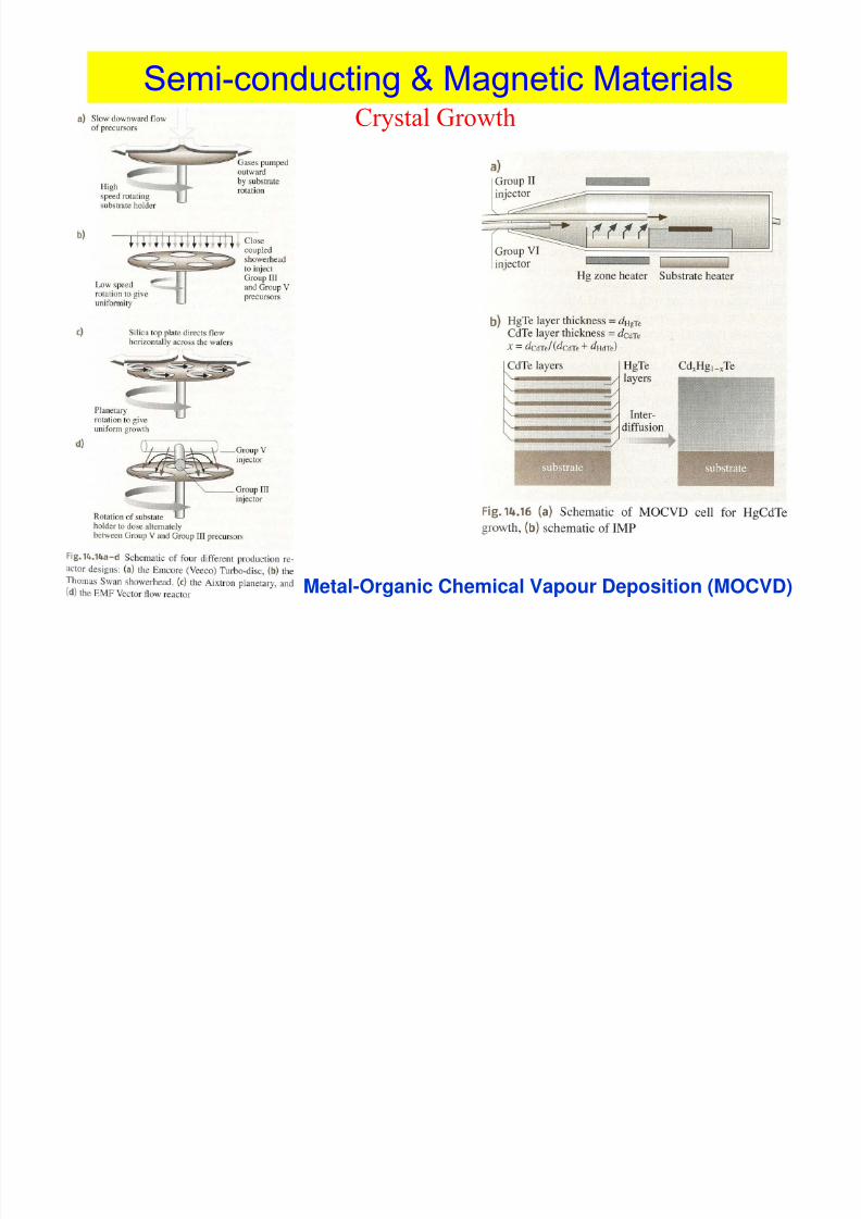
Crystal Growth
Metal-Organic Chemical Vapour Deposition (MOCVD)
Semi-conducting & Magnetic MaterialsC l G h
8/2/2019 Semi Conducting & Magnetic Materials Week 3 Feb 7 2012
http://slidepdf.com/reader/full/semi-conducting-magnetic-materials-week-3-feb-7-2012 68/75
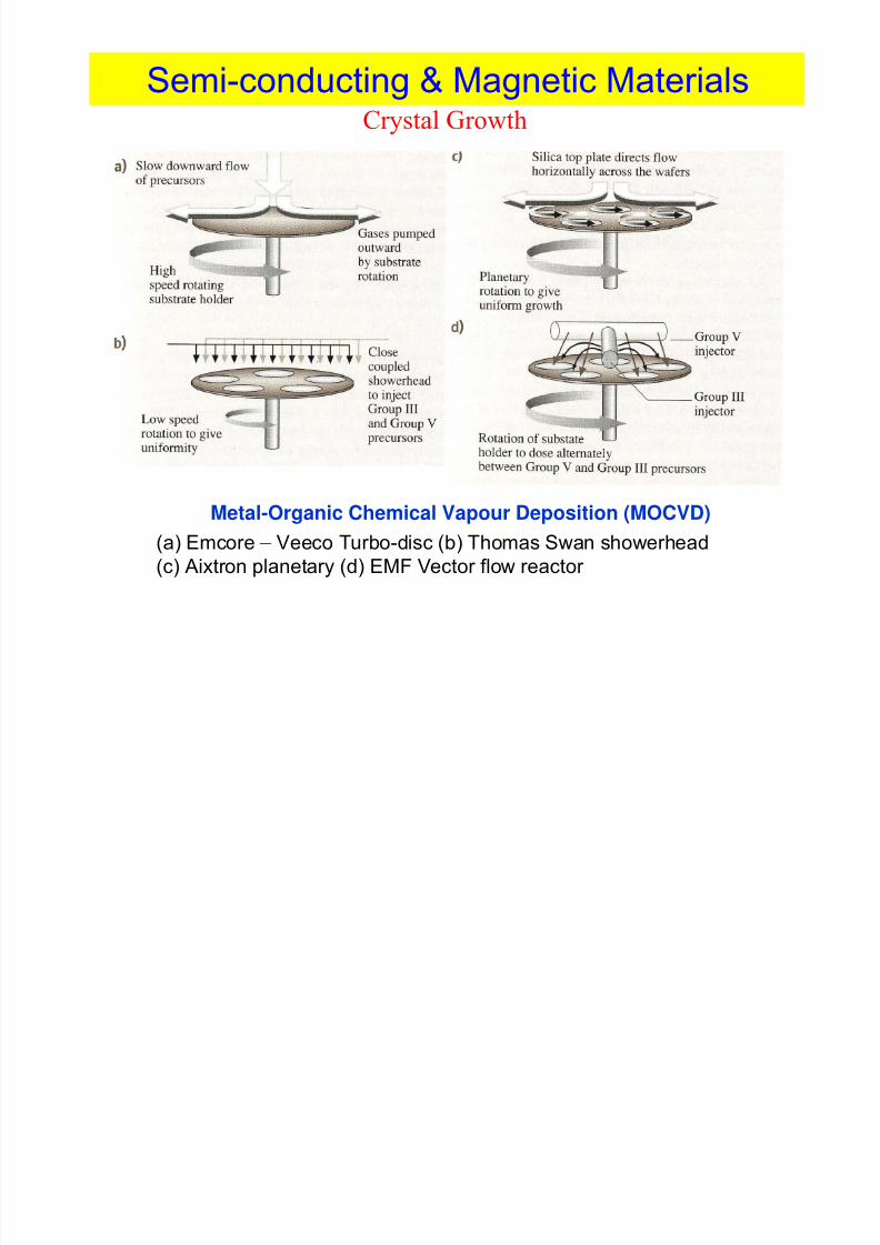
Crystal Growth
Metal-Organic Chemical Vapour Deposition (MOCVD)
(a) Emcore – Veeco Turbo-disc (b) Thomas Swan showerhead
(c) Aixtron planetary (d) EMF Vector flow reactor
Semi-conducting & Magnetic MaterialsC t l G th
8/2/2019 Semi Conducting & Magnetic Materials Week 3 Feb 7 2012
http://slidepdf.com/reader/full/semi-conducting-magnetic-materials-week-3-feb-7-2012 69/75
Crystal Growth
Metal-Organic Chemical Vapour Deposition (MOCVD)
Semi-conducting & Magnetic MaterialsC t l G th

8/2/2019 Semi Conducting & Magnetic Materials Week 3 Feb 7 2012
http://slidepdf.com/reader/full/semi-conducting-magnetic-materials-week-3-feb-7-2012 70/75
Crystal Growth
Metal-Organic Chemical Vapour Deposition (MOCVD)
8/2/2019 Semi Conducting & Magnetic Materials Week 3 Feb 7 2012
http://slidepdf.com/reader/full/semi-conducting-magnetic-materials-week-3-feb-7-2012 71/75
Semi-conducting & Magnetic MaterialsCrystal Growth
8/2/2019 Semi Conducting & Magnetic Materials Week 3 Feb 7 2012
http://slidepdf.com/reader/full/semi-conducting-magnetic-materials-week-3-feb-7-2012 72/75
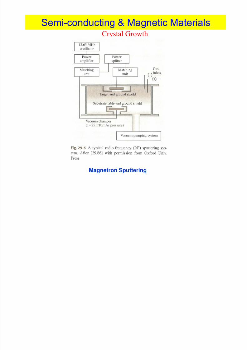
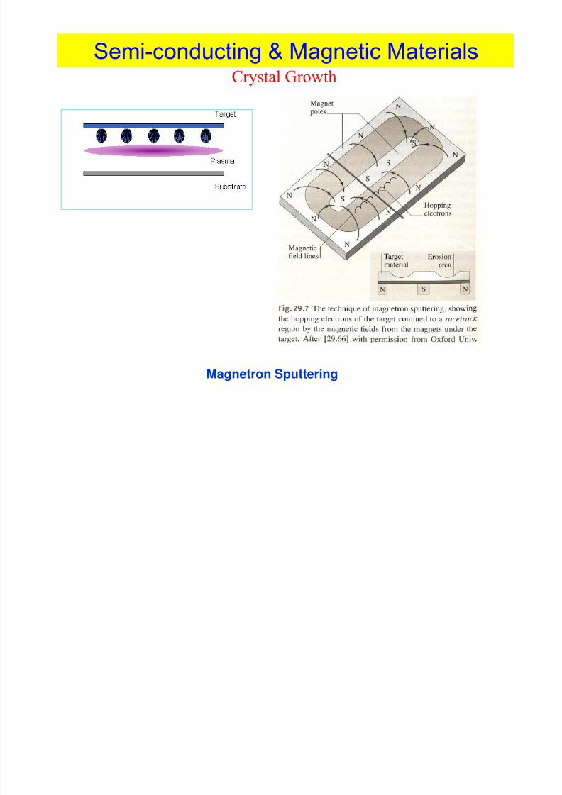
Crystal Growth
Magnetron Sputtering
Semi-conducting & Magnetic MaterialsCrystal Growth
8/2/2019 Semi Conducting & Magnetic Materials Week 3 Feb 7 2012
http://slidepdf.com/reader/full/semi-conducting-magnetic-materials-week-3-feb-7-2012 73/75
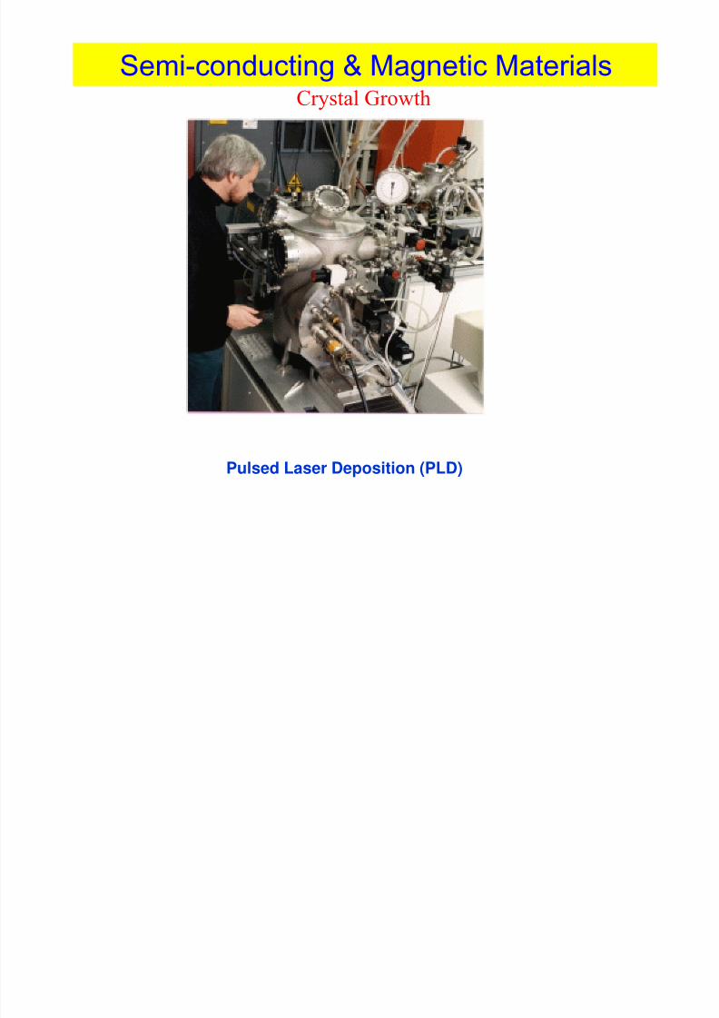
Crystal Growth
Pulsed Laser Deposition (PLD)
Semi-conducting & Magnetic Materials
8/2/2019 Semi Conducting & Magnetic Materials Week 3 Feb 7 2012
http://slidepdf.com/reader/full/semi-conducting-magnetic-materials-week-3-feb-7-2012 74/75
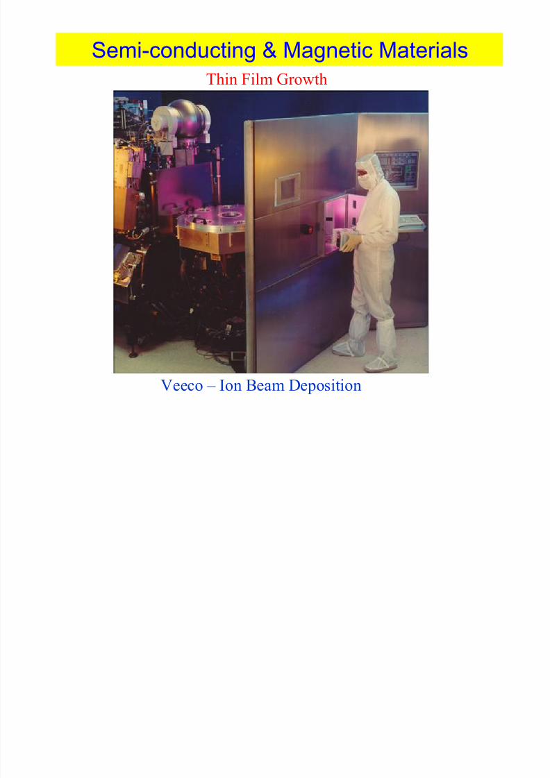
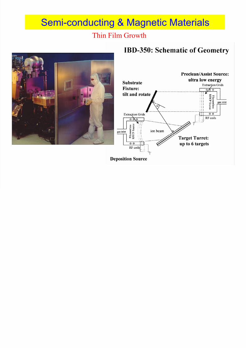
Thin Film Growth
Veeco – Ion Beam Deposition
Semi-conducting & Magnetic Materials
8/2/2019 Semi Conducting & Magnetic Materials Week 3 Feb 7 2012
http://slidepdf.com/reader/full/semi-conducting-magnetic-materials-week-3-feb-7-2012 75/75
Thin Film Growth