Sem2 ic b1_op_amp
38
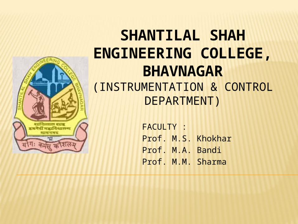
FACULTY : Prof. M.S. Khokhar Prof. M.A. Bandi Prof. M.M. Sharma SHANTILAL SHAH ENGINEERING COLLEGE, BHAVNAGAR (INSTRUMENTATION & CONTROL DEPARTMENT)
-
Upload
jitin-pillai -
Category
Engineering
-
view
37 -
download
1
Transcript of Sem2 ic b1_op_amp
FACULTY :Prof. M.S. KhokharProf. M.A. BandiProf. M.M. Sharma
SHANTILAL SHAH ENGINEERING COLLEGE,
BHAVNAGAR(INSTRUMENTATION & CONTROL
DEPARTMENT)
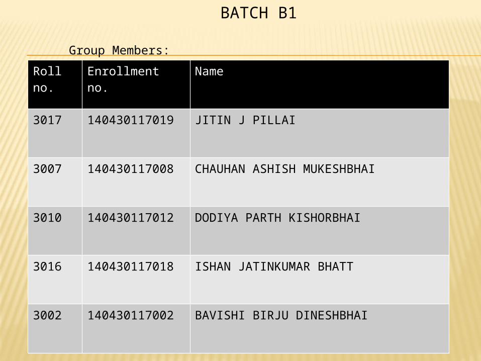
Roll no. Enrollment no. Name
3017 140430117019 JITIN J PILLAI
3007 140430117008 CHAUHAN ASHISH MUKESHBHAI
3010 140430117012 DODIYA PARTH KISHORBHAI
3016 140430117018 ISHAN JATINKUMAR BHATT
3002 140430117002 BAVISHI BIRJU DINESHBHAI
Group Members:
BATCH B1
OPERATIONAL AMPLIFIERS (OP-
AMPS)
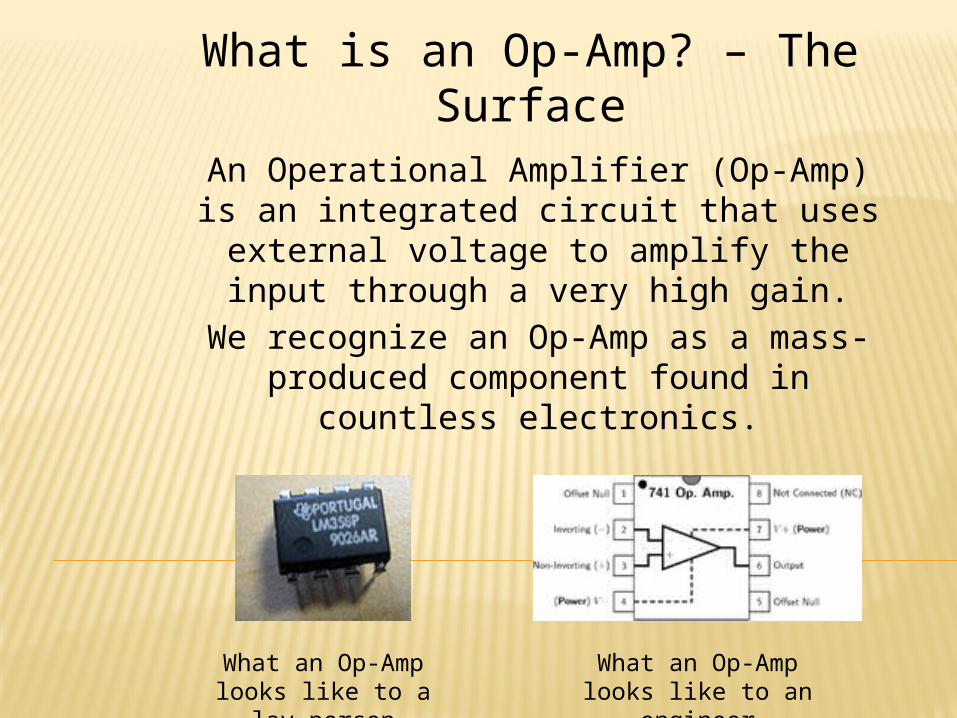
What is an Op-Amp? – The Surface
An Operational Amplifier (Op-Amp) is an integrated circuit that uses external
voltage to amplify the input through a very high gain.
We recognize an Op-Amp as a mass-produced component found in countless
electronics.
What an Op-Amp looks like to a lay-person
What an Op-Amp looks like to an engineer
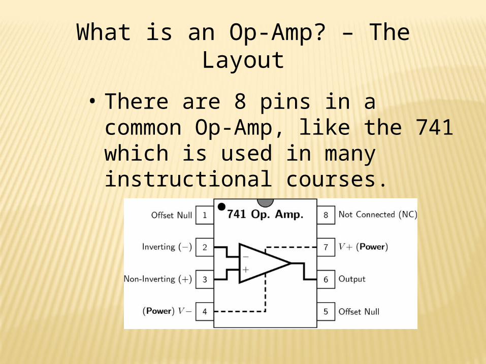
What is an Op-Amp? – The Layout
• There are 8 pins in a common Op-Amp, like the 741 which is used in many instructional courses.
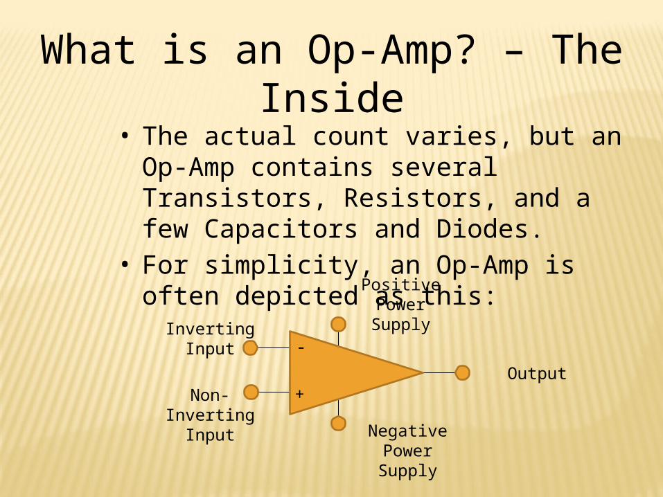
What is an Op-Amp? – The Inside
• The actual count varies, but an Op-Amp contains several Transistors, Resistors, and a few Capacitors and Diodes.
• For simplicity, an Op-Amp is often depicted as this:
Non-Inverting
Input
Inverting Input
Positive Power Supply
Negative Power Supply
Output
-
+
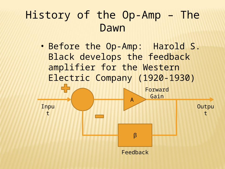
History of the Op-Amp – The Dawn
• Before the Op-Amp: Harold S. Black develops the feedback amplifier for the Western Electric Company (1920-1930)
A
β
Input Output
Forward Gain
Feedback
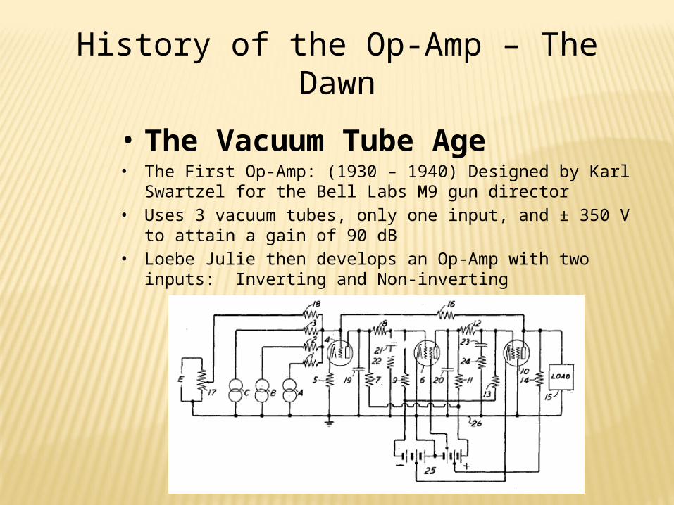
History of the Op-Amp – The Dawn
• The Vacuum Tube Age• The First Op-Amp: (1930 – 1940) Designed by Karl
Swartzel for the Bell Labs M9 gun director• Uses 3 vacuum tubes, only one input, and ± 350 V to
attain a gain of 90 dB• Loebe Julie then develops an Op-Amp with two inputs:
Inverting and Non-inverting
History of the Op-Amp – The Shift
• The end of Vacuum Tubes was built up during the 1950’s-1960’s to the advent of solid-state electronics
1. The Transistor 2. The Integrated Circuit3. The Planar Process
History of the Op-Amp – The Shift
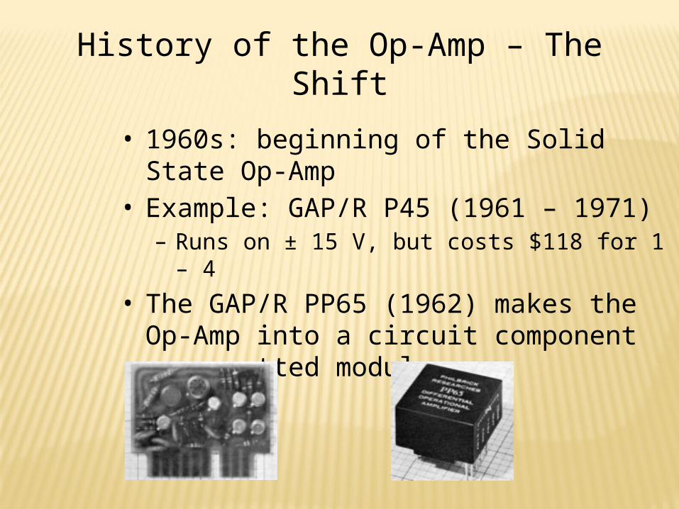
• 1960s: beginning of the Solid State Op-Amp
• Example: GAP/R P45 (1961 – 1971)– Runs on ± 15 V, but costs $118 for 1 – 4
• The GAP/R PP65 (1962) makes the Op-Amp into a circuit component as a potted module
History of the Op-Amp – The Evolution
• The solid-state decade saw a proliferation of Op-Amps– Model 121, High Speed FET family, etc.
• Robert J. Widlar develops the μA702 Monolithic IC Op-Amp (1963) and shortly after the μA709
• Fairchild Semiconductor vs. National Semiconductor– National: The LM101 (1967) and then the LM101A
(1968) (both by Widlar)– Fairchild: The “famous” μA741 (by Dave Fullager 1968)
and then the μA748 (1969)
Mathematics of the Op-Amp
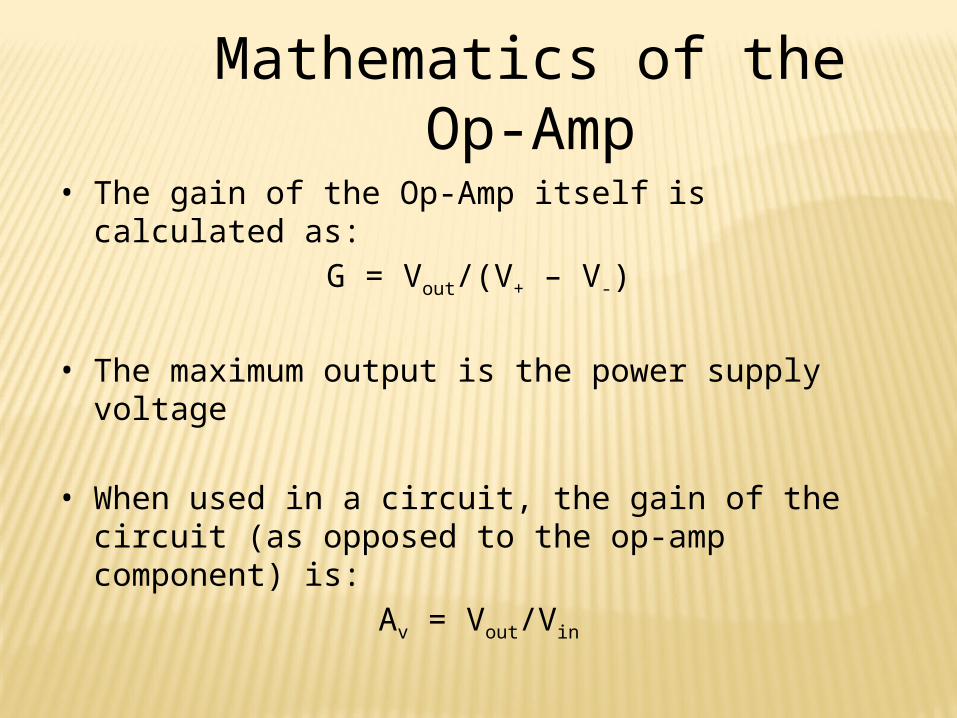
• The gain of the Op-Amp itself is calculated as:G = Vout/(V+ – V-)
• The maximum output is the power supply voltage
• When used in a circuit, the gain of the circuit (as opposed to the op-amp component) is:
Av = Vout/Vin
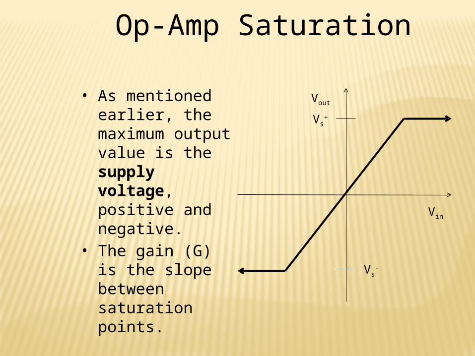
Op-Amp Saturation
• As mentioned earlier, the maximum output value is the supply voltage, positive and negative.
• The gain (G) is the slope between saturation points.
Vout
Vin
Vs-
Vs+
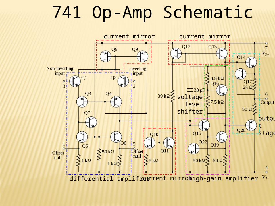
741 Op-Amp Schematic
differential amplifier high-gain amplifier
voltage level
shifteroutput stage
current mirror
current mirror current mirror
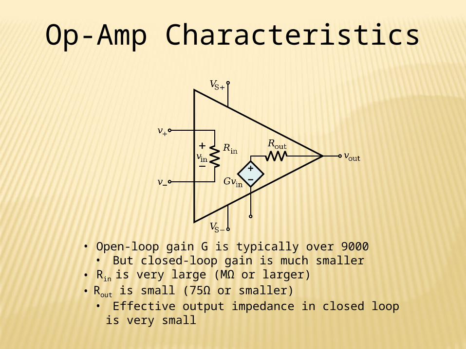
Op-Amp Characteristics
• Open-loop gain G is typically over 9000• But closed-loop gain is much smaller
• Rin is very large (MΩ or larger)• Rout is small (75Ω or smaller)
• Effective output impedance in closed loop is very small
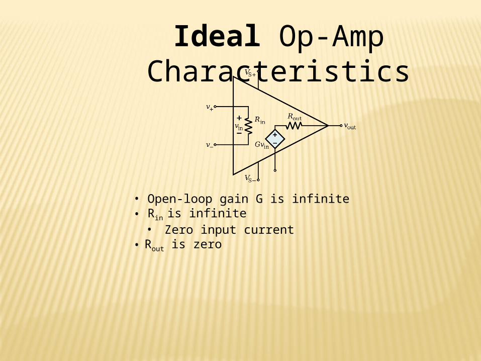
Ideal Op-Amp Characteristics
• Open-loop gain G is infinite• Rin is infinite
• Zero input current• Rout is zero
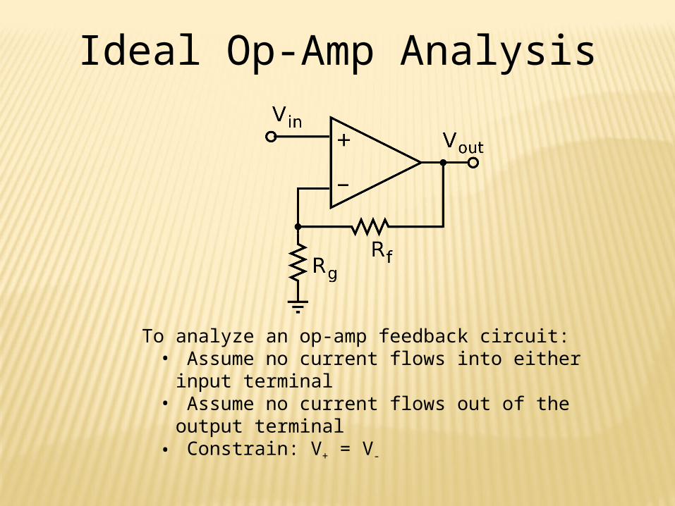
Ideal Op-Amp Analysis
To analyze an op-amp feedback circuit:• Assume no current flows into either input terminal• Assume no current flows out of the output terminal• Constrain: V+ = V-
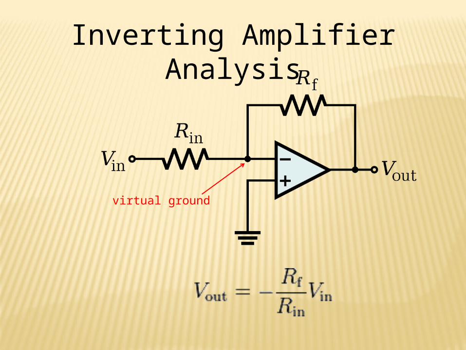
Inverting Amplifier Analysis
virtual ground
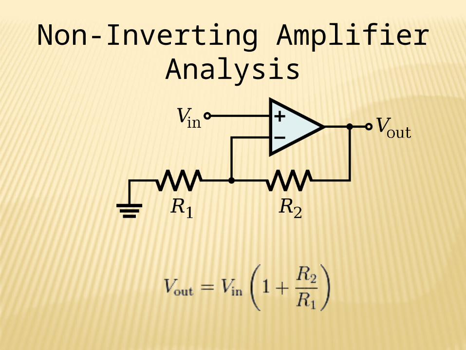
Non-Inverting Amplifier Analysis
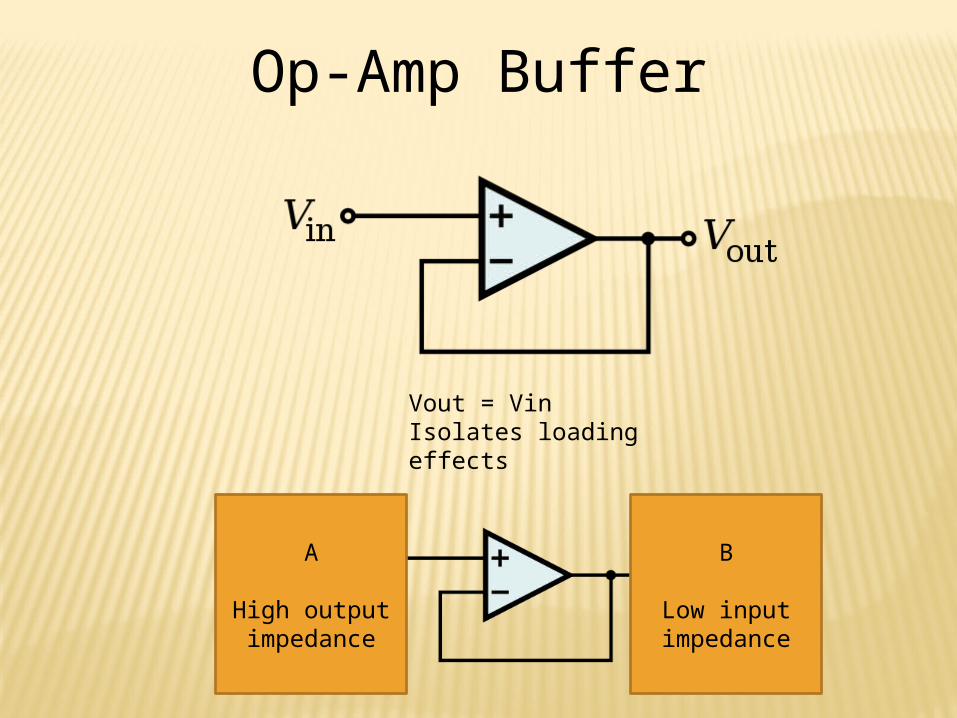
Op-Amp Buffer
Vout = VinIsolates loading effects
A
High output impedance
B
Low input impedance
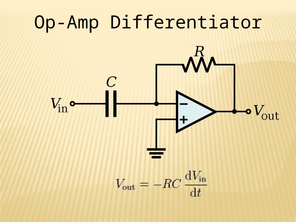
Op-Amp Differentiator
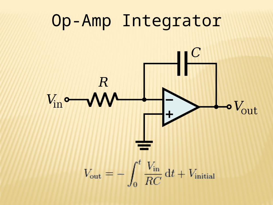
Op-Amp Integrator
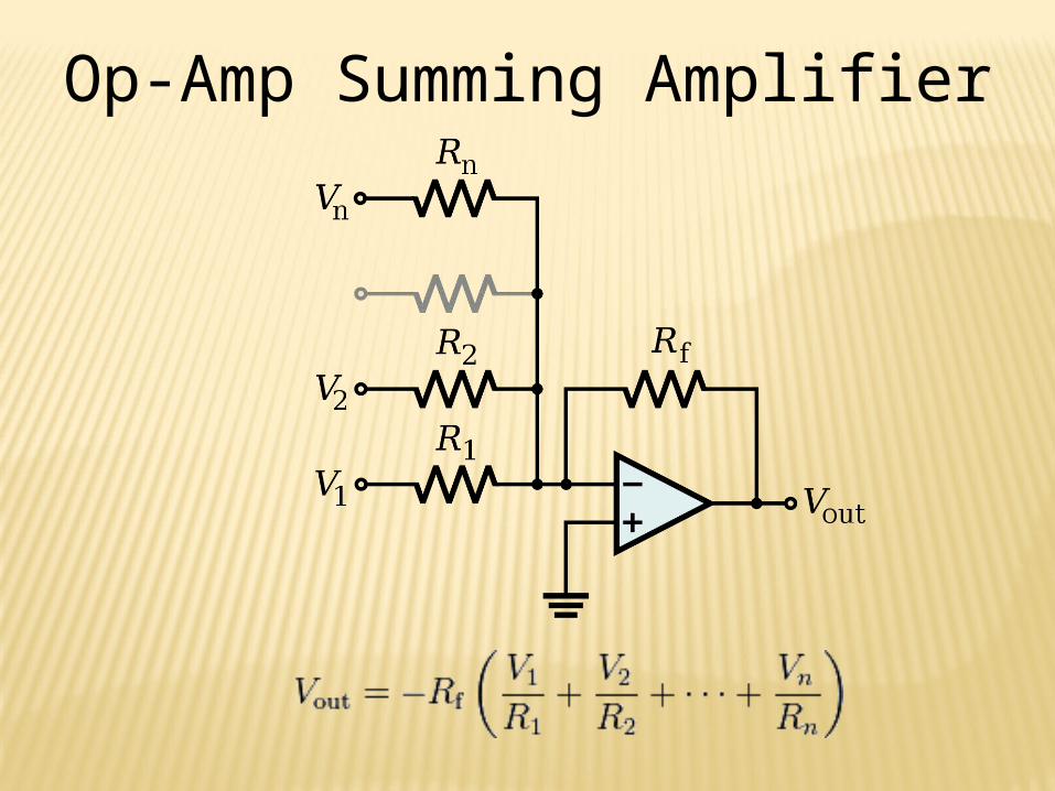
Op-Amp Summing Amplifier
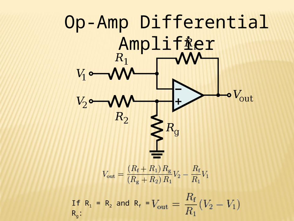
Op-Amp Differential Amplifier
If R1 = R2 and Rf = Rg:
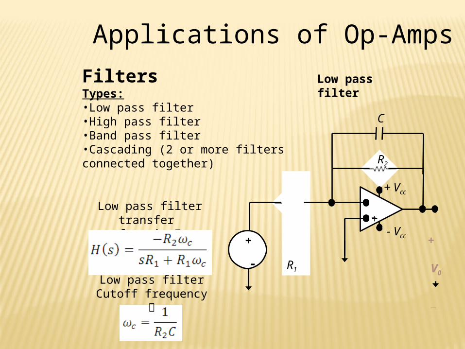
Applications of Op-AmpsFiltersTypes:•Low pass filter•High pass filter•Band pass filter•Cascading (2 or more filters connected together) R2
+
-
+
V0
__
+ Vcc
- Vcc
-+
R1
C
Low pass filter
Low pass filter Cutoff frequency
Low pass filter transfer function
Applications of Op-Amps
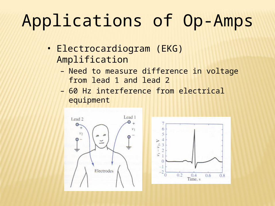
• Electrocardiogram (EKG) Amplification– Need to measure difference in voltage from lead
1 and lead 2– 60 Hz interference from electrical equipment
Applications of Op-Amps
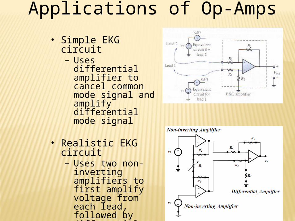
• Simple EKG circuit– Uses differential
amplifier to cancel common mode signal and amplify differential mode signal
• Realistic EKG circuit– Uses two non-
inverting amplifiers to first amplify voltage from each lead, followed by differential amplifier
– Forms an “instrumentation amplifier”
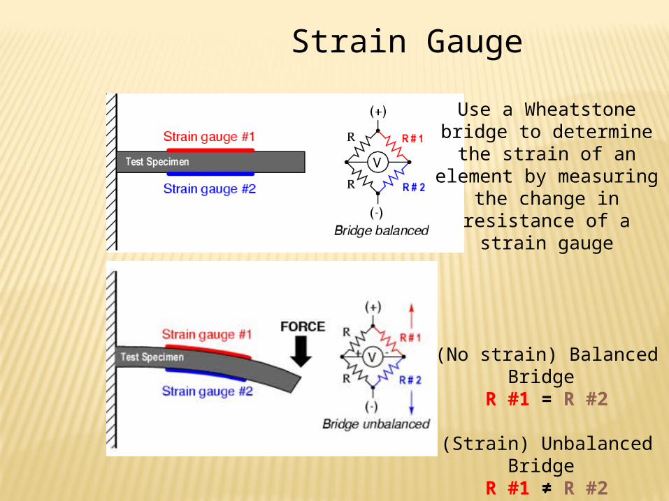
Strain Gauge
Use a Wheatstone bridge to determine the strain of an element by measuring the change in resistance of a strain
gauge
(No strain) Balanced Bridge
R #1 = R #2
(Strain) Unbalanced Bridge
R #1 ≠ R #2
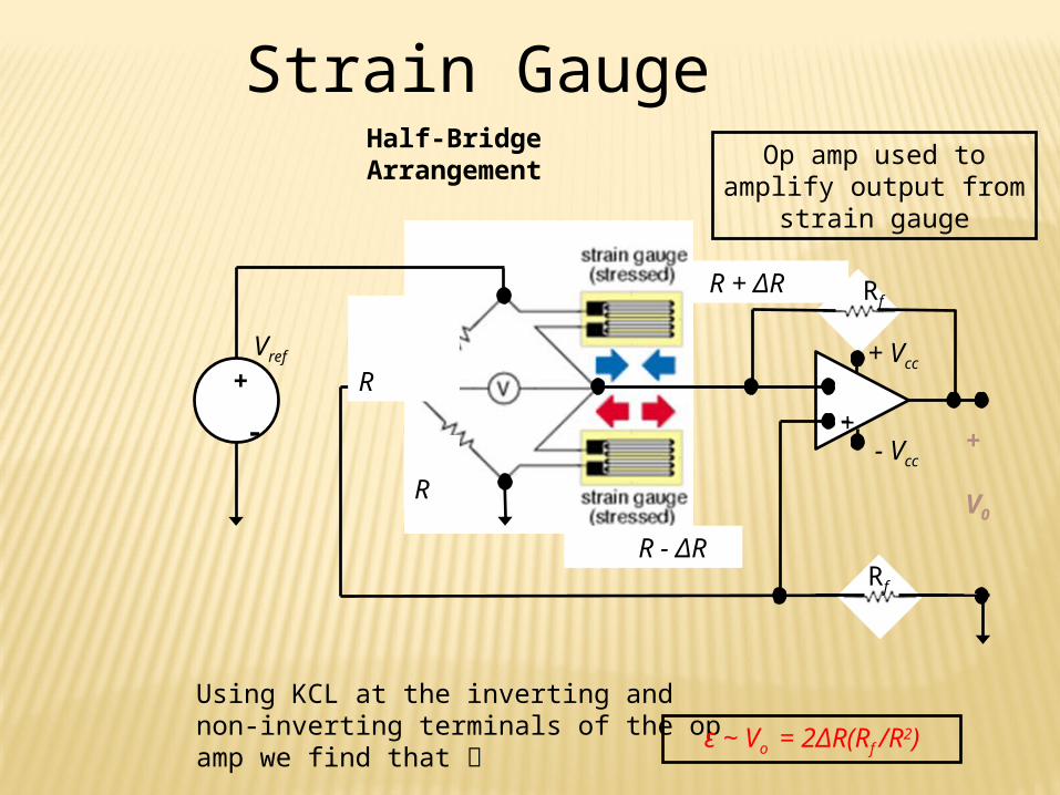
Strain GaugeHalf-Bridge Arrangement
Using KCL at the inverting and non-inverting terminals of the op amp we find that ε ~ Vo = 2ΔR(Rf /R2)
R + ΔR Rf
+
- +
V0
__
+ Vcc
- Vcc
-+
Rf
Vref
R
R - ΔR
R
Op amp used to amplify output from strain gauge
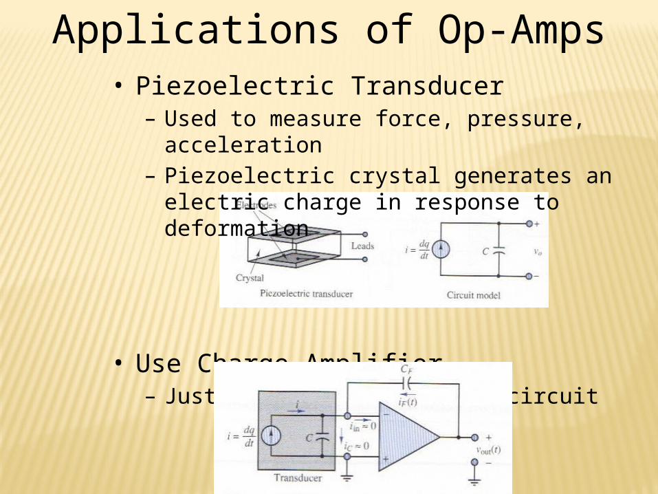
Applications of Op-Amps• Piezoelectric Transducer
– Used to measure force, pressure, acceleration
– Piezoelectric crystal generates an electric charge in response to deformation
• Use Charge Amplifier– Just an integrator op-amp circuit
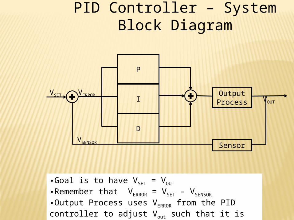
•Goal is to have VSET = VOUT
•Remember that VERROR = VSET – VSENSOR
•Output Process uses VERROR from the PID controller to adjust Vout such that it is ~VSET
P
I
D
Output Process
Sensor
VERRORVSET VOUT
VSENSOR
PID Controller – System Block Diagram
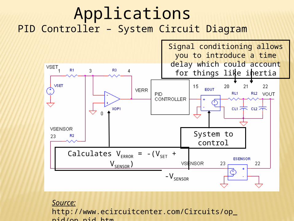
ApplicationsPID Controller – System Circuit Diagram
Source: http://www.ecircuitcenter.com/Circuits/op_pid/op_pid.htm
Calculates VERROR = -(VSET + VSENSOR)
Signal conditioning allows you to introduce a time delay which could
account for things like inertia
System to control
-VSENSOR
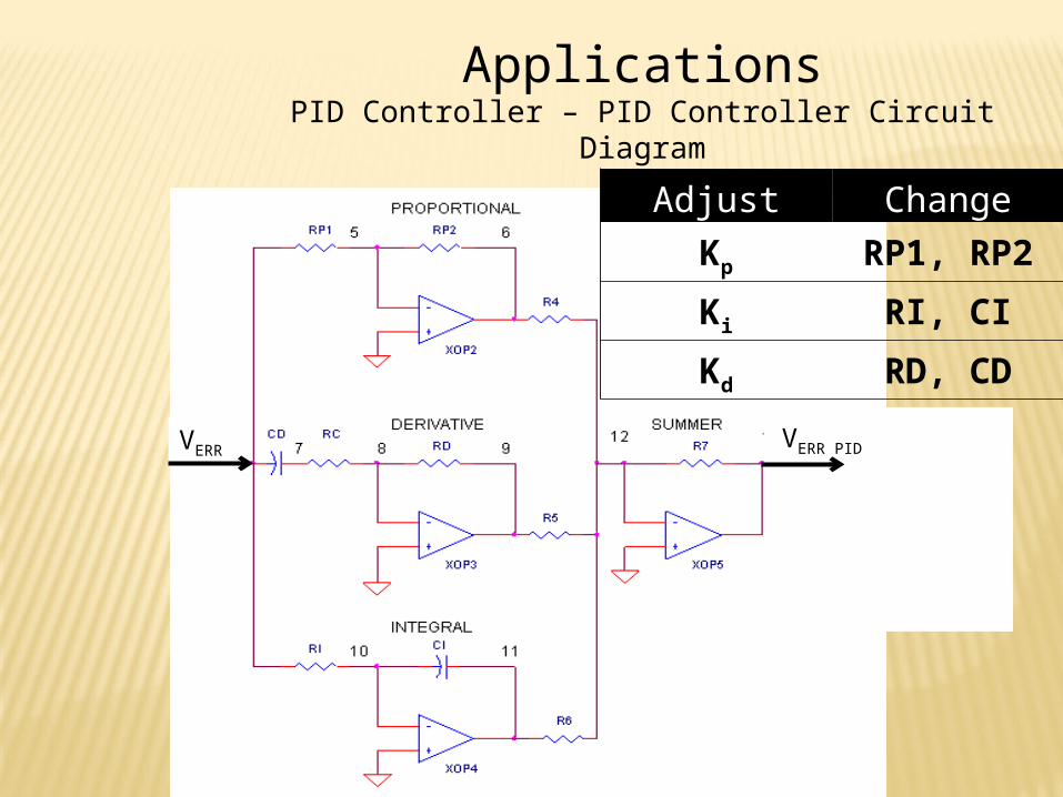
ApplicationsPID Controller – PID Controller Circuit Diagram
VERR
Adjust Change
Kp RP1, RP2
Ki RI, CI
Kd RD, CD
VERR PID
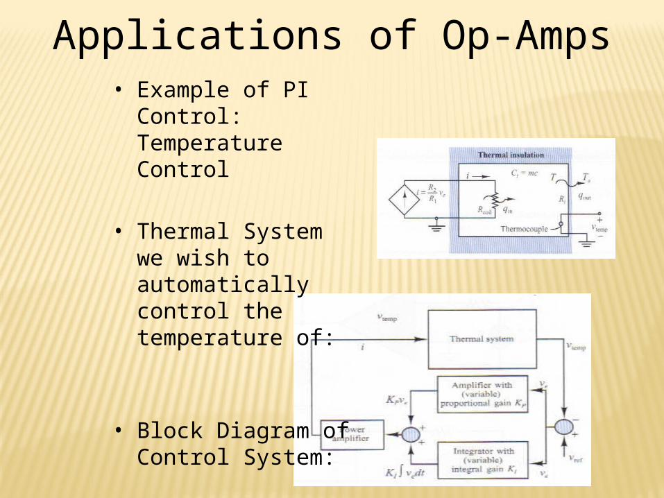
Applications of Op-Amps• Example of PI
Control: Temperature Control
• Thermal System we wish to automatically control the temperature of:
• Block Diagram of Control System:
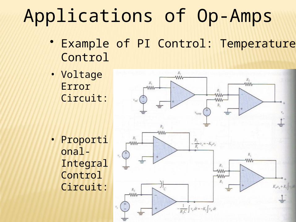
Applications of Op-Amps
• Voltage Error Circuit:
• Proportional-Integral Control Circuit:
• Example of PI Control: Temperature Control

References
• Cetinkunt, Sabri. Mechatronics. Hoboken, NJ: John Wiley & Sons Inc., 2007.
• Jung, Walter G. Op Amp Applications Handbook. Analog Devices, Inc., 2005.
• “Operational Amplifier.” http://en.wikipedia.org/wiki/Operational_amplifier.
• “Operational Amplifier Applications.” http://en.wikipedia.org/wiki/Operational_amplifier_applications.