Self-Oscillating CMOS Class D Amplifier Optimized for Low ...

40 September/October 20131527-3342/13/$31.00©2013IEEE
Digital Object Identifier 10.1109/MMM.2013.2269861Date of publication: 6 September 2013
Self-Oscillating Mixers
The discovery that a single circuit can simultaneously do signal generation and frequency conversion goes all the way back to 1915 when Edwin Armstrong doc-umented how the triode vacuum tube, or
audion, could be designed in a way that “incoming oscillations are simultaneously amplified and com-bined in the system to produce beats with a local oscil-lation continuously maintained” [1]. Today, this type
of circuit is known as a self-oscillating mixer (SOM). In the early days of radio there was good demand for SOMs because they allowed a designer to reduce the overall number of vacuum tubes in a radio receiver. Indeed, the market for SOMs remained profitable well into the 1950s [2]. As solid-state devices steadily changed the economics of the industry, commercial demand for SOMs dried up in the 1960s. Yet, interest in SOMs did not completely disappear after the 1960s. In
Carlos E. Saavedra, Brad R. Jackson,
and Stanley S.K. Ho
Carlos E. Saavedra ([email protected]) is with Queen’s University, Kingston, Ontario, K7L 3N6 Canada. Brad R. Jackson ([email protected]) is with Defence Research and Development Canada, Ottawa, Ontario, K1A 0Z4 Canada.
Stanley S.K. Ho ([email protected]) is with PMC-Sierra, Inc., Burnaby, British Columbia, V5A 4V7 Canada.
Image lIcensed by Ingram PublIshIng
FOCUSED
ISSUE FEATU
RE
September/October 2013 41
fact, important advances in SOM design were carried out by a small number of researchers from the 1970s through the 1990s until, around 2000, interest in SOMs rebounded.
An important factor for the renewed interest in SOMs is their natural fit with active antennas [3]–[6], where low-cost and compact design considerations are paramount. Systems that use active antennas include retrodirective arrays, automotive radars, transpon-ders, and the hardware for that vast application space known as the “Internet of Things (IoT)” [7]–[11]. One way to think about the IoT is that it takes RFID to a new level by enabling two-way communication with tagged
objects over the Internet. The emergence of CMOS as a mainstream RFIC technology has also helped to rein-vigorate SOM development because one can design complex circuits that have high transistor counts while keeping the die area and the dc power consumption under check. CMOS SOMs have advanced to the point that their noise and linearity performance can com-pete with discrete mixer and oscillator blocks.
This article provides an overview of modern SOM circuits. The circuits discussed here fall into one of three broad mixing topologies: unbalanced (UB), sin-gly balanced (SB), and commutating (CM).
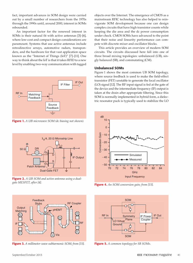
Unbalanced SOMs Figure 1 shows the most common UB SOM topology, where source feedback is used to make the field-effect transistor (FET) unstable to generate the local oscillator (LO) signal [12]. The RF input signal is fed at the gate of the device and the intermediate frequency (IF) output is taken at the drain after appropriate filtering. Since this SOM is normally implemented in hybrid form, a dielec-tric resonator puck is typically used to stabilize the LO
RF In Matching/Feedback
IF FilterIF Out
SourceFeedback
Figure 1. A UB microwave SOM (dc biasing not shown).
Patch Antenna
DR50 X
Dual-Gate FET
S
DIF Output
G2
G1
fLO
mg/4, 20 X Microstrip Line
Figure 2. A UB SOM and active antenna using a dual-gate MESFET, after [4].
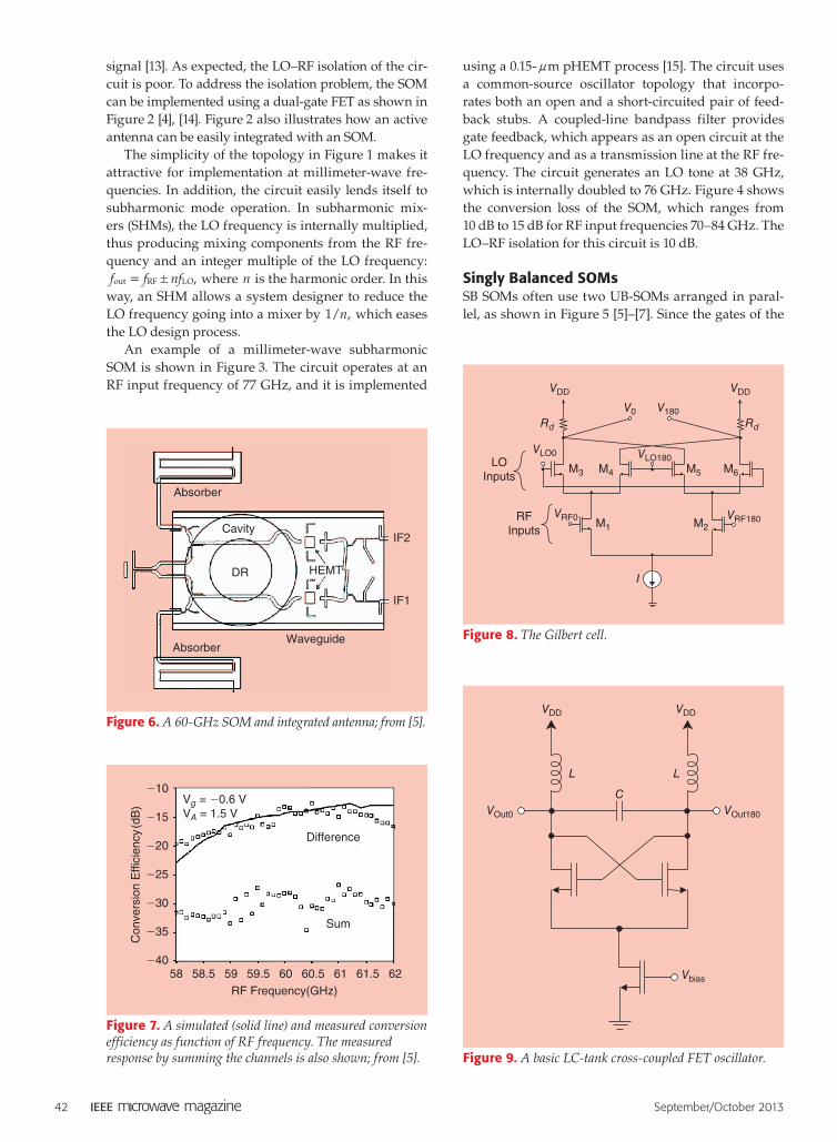
FeedbackStubs
OutputMatching pHEMT
RF Coupler
RF
Via
IF
Figure 3. A millimeter-wave subharmonic SOM; from [15].
dB
Con
vers
ion
Gai
n
10
0
-10
Simulated
Measured
-20
-30
-40
-50
GHz
Input Frequency
70 72 74 76 78 80 82 84
Figure 4. An SOM conversion gain; from [15].
RF In IF Out
SOM
SOM
LO VirtualGround
SymmetryPlane
IF PowerCoupler
Figure 5. A common topology for SB SOMs.
42 September/October 2013
signal [13]. As expected, the LO–RF isolation of the cir-cuit is poor. To address the isolation problem, the SOM can be implemented using a dual-gate FET as shown in Figure 2 [4], [14]. Figure 2 also illustrates how an active antenna can be easily integrated with an SOM.
The simplicity of the topology in Figure 1 makes it attractive for implementation at millimeter-wave fre-quencies. In addition, the circuit easily lends itself to subharmonic mode operation. In subharmonic mix-ers (SHMs), the LO frequency is internally multiplied, thus producing mixing components from the RF fre-quency and an integer multiple of the LO frequency:
,f f nfout RF LO!= where n is the harmonic order. In this way, an SHM allows a system designer to reduce the LO frequency going into a mixer by / ,n1 which eases the LO design process.
An example of a millimeter-wave subharmonic SOM is shown in Figure 3. The circuit operates at an RF input frequency of 77 GHz, and it is implemented
using a 0.15-nm pHEMT process [15]. The circuit uses a common-source oscillator topology that incorpo-rates both an open and a short-circuited pair of feed-back stubs. A coupled-line bandpass filter provides gate feedback, which appears as an open circuit at the LO frequency and as a transmission line at the RF fre-quency. The circuit generates an LO tone at 38 GHz, which is internally doubled to 76 GHz. Figure 4 shows the conversion loss of the SOM, which ranges from 10 dB to 15 dB for RF input frequencies 70–84 GHz. The LO–RF isolation for this circuit is 10 dB.
Singly Balanced SOMs SB SOMs often use two UB-SOMs arranged in paral-lel, as shown in Figure 5 [5]–[7]. Since the gates of the
Vg = -0.6 VVA = 1.5 V
Difference
Sum
58
Con
vers
ion
Effi
cien
cy(d
B)
-40
-35
-30
-25
-20
-15
-10
58.5 59 59.5 60RF Frequency(GHz)
60.5 61 61.5 62
Figure 7. A simulated (solid line) and measured conversion efficiency as function of RF frequency. The measured response by summing the channels is also shown; from [5].
VDD VDD
VLO0
V0 V180
VRF0
VLO180
VRF180
M3LO
Inputs
RFInputs
M4 M5
M2M1
I
M6
Rd Rd
Figure 8. The Gilbert cell.
VDD VDD
C
L L
VOut0 VOut180
Vbias
Figure 9. A basic LC-tank cross-coupled FET oscillator.
Absorber
Cavity
DR HEMT
IF2
IF1
WaveguideAbsorber
Figure 6. A 60-GHz SOM and integrated antenna; from [5].

September/October 2013 43
two UB-SOMs are connected together, the LO signals are synchronized through injection locking [16]. Note that the SB-SOM is symmetric about the horizontal axis, which creates a virtual ground for the LO signal half way between the transistor gates. When the two UB-SOMs lock together, the LO signals are 180° out of phase, thus providing the SB-SOM with a differential LO signal. The IF outputs of the two mixers are com-bined using an IF balun that constructively combines the odd-order mixing products and destructively com-bines the even-order components. Like its constituent UB-SOMs, the SB-SOM can also operate in subhar-monic mode.
A 60-GHz SB-SOM with an integrated quasi-Yagi antenna is depicted in Figure 6 [5]. The antenna picks up the RF signal and feeds it to the SOM. The LO sig-nal is stabilized by means of a dielectric resonator and, to save space, the puck is shared by the two UB-SOMs. A hybrid coupler, not shown in Figure 6, is used to pro-duce the sum and difference of the mixing products, IF1 and IF2 from the two transistors. The conversion gain of this SOM cannot be measured directly because the RF signal is fed through the antenna as opposed to a connectorized port. Instead, a different quantity must be defined: the conversion efficiency, which merges the concepts of antenna efficiency and mixer conversion gain. The measured conversion efficiency for this SOM is shown in Figure 7.
CMOS Commutating SOMs The arrival of CMOS technology into the microwave design space has opened the way to new ideas in SOM circuit design [17]–[22]. The starting point in the design
of many CMOS SOMs is the classic CM active mixer shown in Figure 8, also known to designers as the Gilbert cell [23]. It is an excellent mixer that is widely used in RFICs for telecom systems because of its high
Switching Core
Load
VIF
VRF
+ -
+
+
-
-VLO
VDD
Figure 10. Type I SOM: the oscillator is below the RF input stage.
Oscillator Load
Switching Core
Transconductance StageVRF
+
-
+
+ -
-
+ -
VDD
VIF
VLO
Figure 11. Type II SOM: the oscillator is stacked above the switching core.
VRF
gm1 gm2 gm3 gm4
VRF
VIF
VRF
VLO VLO
Figure 12. Functional representation of the type I SOM; from [17].

44 September/October 2013
conversion gain, high port-to-port isolation, high lin-earity, and broadband frequency response. The basic Gilbert cell has a poor noise figure (NF), but the NF can be significantly improved by using noise-reduction design techniques (see, for example [21], [24], and [25]).
Signal generation in CM SOMs involves some type of LC-tank oscillator, a simple version of which is shown in Figure 9. In this oscillator, the resistance looking into the cross-coupled pair is / ,g2 m- where gm is the transconductance of each of the cross-cou-pled FETs. Therefore, with appropriate device sizing and biasing, the negative resistance produced by the cross-coupled pair can be designed to cancel out the resistive loss in the LC tank, thereby producing sus-tained oscillations.
The majority of CM-SOMs are based on one of two general configurations, which we will call type I and II. In type I SOMs, the oscillator is below the RF input stage as shown in Figure 10. In type II SOMs, the oscillator is stacked above the switching core and replaces the load network as depicted in Figure 11.
Pha
se N
oise
(dB
c/H
z)
Frequency Offset1 MHz 10 MHz100 KHz
-150
-130
-110
-90
-70
Figure 14. Oscillator phase noise of the SOM in [17].
0° 180°
Mixer
fRF
2fLO 2fLO
Local Oscillator
fLO fLO
VC VC
fIF
0° 0°
180° 180°
VC VC
Figure 15. A block diagram of the dual-band self-oscillating mixer in [19].
VDD1
L2 L1
VDD2
VCont
VDD2
VDD2
RL/2 RL/2
RS RS
1
1
CVC
22
VIF
VRFM1
M5
VCO
M7 M8
M6
M2 M3 M4
Mixer
VG
RG VG
RG
VRF
Figure 13. A schematic diagram of the CMOS SOM in [17].

September/October 2013 45
In type I SOMs, the LO and RF inputs into the switching core are flipped relative to the standard Gilbert cell structure. A functional representation of the type I SOM is shown in Figure 12. A benefit of this approach is that less LO signal power is needed that,
of course, also saves dc power. One of the first type I SOMs was implemented using bipolar devices [26], and CMOS versions followed some years later [17]. A schematic diagram of the SOM reported in [17] is shown in Figure 13. There, transistors M1 –M4 are the
Figure 18. A chip photograph of the dual-band SOM; from [19].
4.5 5 5.5 6-10
-5
0
5
10
15
20
Con
vers
ion
Gai
n (d
B)
10 10.5 11 11.5 12RF Frequency (GHz)
Figure 17. Conversion gain of the dual-band SOM; from [19].
VDD
VDD
VSHC
VDD
VDD
Sw1
Sw2
Sw3 Sw4
VDD
VDD
VDD VDD VDD
VC
L C C
CM1 CM2
L LL
VC
Rb Rb
Rb Rb
VIF+ VIF-
Rd Rd
VDD
0°
0° 180°
180°RF
Inputs
VC
Figure 16. A circuit schematic of the proposed dual-band self-oscillating mixer; from [19].
VDD
M1
M3
IF+ -
M4
M5
CdM2
RFin
Lg
LSZin
Figure 19. A low-noise self-oscillating mixer, after [18].

46 September/October 2013
RF transconductor devices, M5 and M6 are cross-cou-pled devices for the oscillator and M7 –M8 are buffers to measure the LO signal. The SOM operates at an RF input frequency of 4.2 GHz, it has a conversion gain close to 11 dB and consumes a total of 3.14 mW of dc power. The phase noise performance of the oscillator in this SOM is shown in Figure 14.
The block diagram of a type I SOM that can oper-ate in fundamental and subharmonic modes is shown in Figure 15 [19]. The switches are turned on and off in a complementary fashion so that either the funda-mental LO tone, ,f0 or its second harmonic, ,f2 0 are fed to the mixing core. A detailed schematic of the circuit is depicted in Figure 16. The SOM uses two LC-tank oscillators that are synchronized through injection coupling at f2 0 through the cross-coupled transistors at the tails of the LC oscillators. By enforc-ing a 180° relationship at f2 0 in the two otherwise separate oscillator circuits, a quadrature relationship between the fundamental outputs at f0 is obtained [27], [28]. This method of locking the oscillators at f2 0 is known as “superharmonic coupling,” and it can also be done using passive transformers [29]–[31]. The advantage of using transistors for injection locking is less die area compared to using transformers, but the latter choice offers better oscillator phase-noise performance.
The conversion gain of this circuit is shown in Figure 17, and it varies from 5 to 12 dB over an aggre-gate bandwidth of 3.3 GHz, covering the ranges 5–6 GHz and 9.5–11.8 GHz. The LO–RF isolation of this circuit is 40.3 dB when it operates in fundamen-tal mode and 36.7 dB in subharmonic mode. A photo-graph of the chip is shown in Figure 18, and its area is 0.525 mm2, including bonding pads.
The circuit schematic of a type II SOM is depicted in Figure 19 [18]. Here, M1 –M2 are the cross-coupled devices for the oscillator circuit, and M3 –M4 consti-tute the switching core of a single-balanced mixer. The source terminals of M1 and M2 are interconnected via a capacitor Cd to provide a path for the LO signal to flow around the loop, while at the IF frequency, Cd is a high impedance. A plot of the phase noise of this oscillator is shown in Figure 20, and it is comparable to the phase-noise plot shown in Figure 14. This leads to the simple observation that, with regard to oscilla-tor phase noise, the difference between type I or type II SOM topology is not too significant. Transistor M5 in Figure 19 is arranged as a low-noise RF transcon-ductor to reduce the noise figure of the mixer. It is a well-known CMOS low-noise amplifier configuration [32] in which the inductances Ls and ,Lg the transistor
(a) (b)
Figure 22. Transforming one cross-coupled pair into two cross-coupled pairs: (a) splitting one device into two parallel devices and (b) rearranging the topology.
Pha
se N
oise
(dB
c/H
z)
-40
-60
-80
-100
-120
-140
Frequency (MHz)
-104 dBc/Hz@1MHz
0.01 0.1 1 10
Figure 20. The oscillator phase noise of the SOM in Figure 19; from [18].
LC Oscillator
CurrentBleedingCircuit
Low-Noise Transconductors
VDD
V+LO V-LO
V+IF V-IF
V+RF V-RF
Figure 21. A block diagram of the low-noise SOM; from [21].
An important factor for the renewed interest in SOMs is their natural fit with active antennas, where low-cost and compact design considerations are paramount.

September/October 2013 47
dimensions /W L , and the bias voltages are design variables used to obtain the optimal noise and imped-ance match. The popularity of this low-noise ampli-fier (LNA) topology is such that various methods have been developed to simultaneously optimize its noise and impedance match [33].
The block diagram of a double-balanced, broad-band, type II SOM is depicted in Figure 21 [22]. Since this SOM is fully differential, in contrast to the one in Figure 19 which is SB, the basic oscillator circuit in Figure 9 needs to be modified before it can be stacked on top of the switching core. The first step is to split each transistor in the cross-coupled pair into
two parallel transistors as shown in Figure 22(a). The second step is to rearrange the topology as shown in Figure 22(b) to get two cross-coupled pairs that share the same LC-tank. The advantage of this approach is that it is equivalent to having two parallel LC-tank oscillators but relying on only one LC-tank, thereby saving a noticeable amount of chip area. More impor-tantly, this new configuration can be connected to the mixer core to act as a fully balanced load. The dc cur-rent through the left- and right-hand side of the oscilla-tor is half of the original value, and the transistor gate widths are also appropriately scaled. The detailed cir-cuit schematic of this SOM is shown in Figure 23.
VDD BufferBuffer SOM Core
VDD
VBld VBld
LShunt
VDD
LTank2Cp
2CVar 2CVar
2Cp
VTune
V+IF
V+LO V+LOV-LO
V-IFM13
M9
M3
M7
M1 M2
M4 M5 M6
M8
M14
M10 M11 M12
R1 C1 C2 R2
C3
Lg Lg
LS LS
C4
V+RF V-RF
Figure 23. A circuit diagram of the low-noise SOM; from [21].
7.8 8 8.2 8.4 8.6 8.80
5
10
15
RF Input Frequency (GHz)
Con
vers
ion
Gai
n (d
B)
0
5
10
15
DS
B N
oise
Fig
ure
(dB
)
MeasurementSimulation
Figure 24. Measured and simulated DSB NF and CG for the SOM in [21]. Figure 25. Chip photo of the low-noise SOM; from [21].

48 September/October 2013
A key design goal for any SOM is to minimize its NF. In the noise theory of CM mixers, the LO wave-form plays a dominant role in the level of thermal and flicker noise produced by the mixer [34], [35]. The impact of the LO signal on the mixer’s noise per-formance is often called “switching noise” because the LO signal controls the transient response of the switching devices. The switching noise can be reduced by minimizing the dc current through the switches and by making the LO have sharp high/low transitions. A high current is needed to mitigate the NF of the transconductor stage below the switching core. One way to meet these opposing demands on the mixer’s dc current is to use current bleeding. In Figure 23, transistors M7 and M8 form the current bleeding subcircuit whose purpose is to inject extra dc current into the bottom transconductors. This allows the switching devices M3 –M6 to be biased with a lower overdrive voltage and, by extension, a lower dc current. In this manner, less LO power is needed for switching, which makes the switching more ideal. The series inductor between the drain terminals of M1 and M2 resonates with the drain capacitance of the two devices, which helps to reduce the flicker noise of the mixer. Applying these design techniques yields a low SOM NF and a good conversion gain over
a broad bandwidth. Figure 24 shows the measured conversion gain and double sideband (DSB) NF of the SOM under discussion as a function of frequency. A photograph of the chip, which measures 0.47 mm2 in area, is shown in Figure 25. A comparison table of recent SOMs is shown in Table 1.
Conclusion The prospect of reducing the parts count, power consumption, and cost of a system by merging the mixing and signal generation functions into one cir-cuit block explains the lasting appeal of SOMs. The widespread popularity of SOMs in the first half of the 20th century was because the economics of the electronics industry at the time made them com-petitive in the marketplace. The arrival of solid-state devices changed the dynamic, and SOMs became more of a curiosity for a good while until the turn of the 21st century. SOMs have a promising future again because they are a natural fit for active anten-nas, whose most intriguing application these days is the IoT. Technologies related to radar and telecom-munications also stand to benefit from the recent advances in CMOS SOMs because their performance, when evaluated at the system level, is now compa-rable to using individual mixer and oscillator blocks.
Table 1. Modern SOM performance summary.
ReferenceCircuit Type Technology fRF (GHz)
Mixing Order
Conv. Gain (dB)
DC Power (mW) NF (dB)
PN* dBc/Hz)
IIP3 (dBm)
LO–RF Iso. (dB)
Size (mm2 )
[15] UB pHEMT 0.15 nm
70–85 2 -15.0 — — -76 — -10 2.0
[36] SB Hybrid 5.8 3 11.1 32 6.9 — — — —
[37] SB Hybrid 24.6–25.5 2 -15 52 — — — — —
[17] CM CMOS 0.18 nm
4.1–4.6 1 10.9 3.14 14.5 -80 -11.8 -37 0.96
[19] CM CMOS 0.13 nm
5–6 9.8–11.8
12
1212
6868
8.710.9
——
23
-40-37
0.530.53
[20] CM CMOS 0.13 nm
25.8–30.1 1 26.4 — — -100 — — —
[21] CM CMOS 0.13 nm
7.8–8.8 1 11.6 12 4.3 -90 -8.3 -59 0.47
[22] CM SiGe 20.1–21.9 1 -10.5 313.5 — -75 — — 1.1
[38] UB Hybrid 30 2 -12 22 — -81 — -50 —
[39] UB Hybrid 5.79 3 11.5 9 — — — — —
[40] UB Hybrid 10.6–11.8 3 2.5 43 — — 9.5 — —
[41] UB Hybrid 4.5 3.25
23
5.959.75
——
——
——
——
——
——
[42] CM InGaP/GaAs 2.34–2.54 1 15 60 — -84 -5 — 1.98*Phase noise (PN) values are quoted for a 100-kHz offset.

September/October 2013 49
References[1] E. Armstrong, “Some recent developments in the audion receiver,”
Proc. IRE, vol. 3, no. 3, pp. 215–238, Sept. 1915.[2] D. E. Sunstein, “A new self-oscillating frequency converter,” IRE
Trans. Broadcasting Telev. Receiv., vol. BTR-1, no. 1, pp. 29–35, Jan. 1955.[3] J. Lin and T. Itoh, “Active integrated antennas,” IEEE Trans. Micro-
wave Theory Tech., vol. 42, no. 12, pp. 2186–2194, Dec. 1994.[4] J. Zhang, Y. Wang, and Z. Chen, “Integration of a self-oscillating
mixer and an active antenna,” IEEE Microwave Guided Wave Lett., vol. 9, no. 3, pp. 117–119, Mar. 1999.
[5] M. Sironen, Y. Qian, and T. Itoh, “A subharmonic self-oscillating mixer with integrated antenna for 60-GHz wireless applications,” IEEE Trans. Microwave Theory Tech., vol. 49, no. 3, pp. 442–450, Mar. 2001.
[6] W. Choi, C. Cheon, and Y. Kwon, “A V-band MMIC self oscillating mixer active integrated antenna using a push-pull patch antenna,” in Proc. IEEE Int. Microwave Symp., 2006, pp. 630–633.
[7] S.-C. Yen and T.-H. Chu, “A retro-directive antenna array with phase conjugation circuit using subharmonically injection-locked self-oscillating mixers,” IEEE Trans. Antennas Propagat., vol. 52, no. 1, pp. 154–164, Jan. 2004.
[8] Y. Yan, Y. B. Karandikar, S. E. Gunnarsson, and H. Zirath, “24 GHz balanced self-oscillating mixer with integrated patch an-tenna array,” in Proc. European Microwave Conf., 2011, pp. 404–407.
[9] C. Wu, Y. Dong, and T. Itoh, “Transponder using SIW based nega-tive and zeroth order resonance dual-band antenna and sub-har-monic self-oscillating mixer,” in Proc. Asia-Pacific Microwave Conf., 2011, pp. 1218–1221.
[10] E. Welbourne, L. Battle, G. Cole, K. Gould, K. Rector, S. Raymer, M. Balazinska, and G. Borriello, “Building the Internet of Things using RFID: The RFID ecosystem experience,” Internet Comput., vol. 13, no. 3, pp. 48–55, Mar. 2009.
[11] Z. Zou, D. S. Mendoza, P. Wang, Q. Zhou, J. Mao, F. Jonsson, H. Tenhunen, and L.-R. Zheng, “A low-power and flexible energy detection IR-UWB receiver for RFID and wireless sensor net-works,” IEEE Trans. Circuits Syst. I, vol. 58, no. 7, pp. 1470–1482, July 2011.
[12] I. Higgins, “Performance of self-oscillating GaAs M.E.S.F.E.T. mixers at X-band,” Electron. Lett., vol. 12, no. 23, pp. 605–606, Nov. 1976.
[13] Y. Tajima, “GaAs FET applications for injection-locked oscillators and self-oscillating mixers,” IEEE Trans. Microwave Theory Tech., vol. 27, no. 7, pp. 629–632, July 1979.
[14] C. Tsironis, “12 GHz receiver with self-oscillating dual-gate MES-FET mixer,” Electron. Lett., vol. 17, no. 17, pp. 617–618, 1981.
[15] M. J. Roberts, S. Iezekiel, and C. M. Snowden, “A compact sub-harmonically pumped MMIC self oscillating mixer for 77 GHz applications,” in Proc. IEEE Int. Microwave Symp., 1998, vol. 3, pp. 1435–1438.
[16] K. S. Ang, M. Underhill, and I. Robertson, “Balanced monolithic oscillators at K- and Ka-band,” IEEE Trans. Microwave Theory Tech., vol. 48, no. 2, pp. 187–193, Feb. 2000.
[17] T.-P. Wang, C.-C. Chang, R.-C. Liu, M.-D. Tsai, K.-J. Sun, Y.-T. Chang, L.-H. Lu, and H. Wang, “A low-power oscillator mixer in 0.18-μm CMOS technology,” IEEE Trans. Microwave Theory Tech., vol. 54, no. 1, pp. 88–95, Jan. 2006.
[18] A. Liscidini, A. Mazzanti, R. Tonietto, L. Vandi, P. Andreani, and R. Castello, “Single-stage low-power quadrature RF receiver front-end: The LMV cell,” IEEE J. Solid-State Circuits, vol. 41, no. 12, pp. 2832–2841, Dec. 2006.
[19] B. R. Jackson and C. E. Saavedra, “A dual-band self-oscillating mixer for C-band and X-band applications,” IEEE Trans. Microwave Theory Tech., vol. 58, no. 2, pp. 318–323, Feb. 2010.
[20] J.-Y. Kim and W.-Y. Choi, “30 GHz CMOS self-oscillating mixer for self-heterodyne receiver application,” IEEE Microwave Wireless Comp. Lett., vol. 20, no. 6, pp. 334–336, June 2010.
[21] S. S. K. Ho and C. E. Saavedra, “A low-noise self-oscillating mixer using a balanced VCO load,” IEEE Trans. Circuits Syst. I, Reg. Papers, vol. 58, no. 8, pp. 1705–1712, Aug. 2011.
[22] F. Starzer, H. Forstner, L. Maurer, and A. Stelzer, “A 21-GHz self-oscillating down-converter mixer,” in Proc. IEEE Topical Meeting Silicon Monolithic Integrated Circuits RF System, Jan. 2012, pp. 93–96.
[23] B. Gilbert, “A precise four-quadrant multiplier with subnanosec-ond response,” IEEE J. Solid-State Circuits, vol. 3, no. 4, pp. 365–373, Dec. 1968.
[24] H. Sjoland, A. Karimi-Sanjaani, and A. Abidi, “A merged CMOS LNA and mixer for a WCDMA receiver,” IEEE J. Solid-State Circuits, vol. 38, no. 6, pp. 1045–1050, June 2003.
[25] S. Ho and C. Saavedra, “A CMOS broadband low-noise mixer with noise cancellation,” IEEE Trans. Microwave Theory Tech., vol. 58, no. 5, pp. 1126–1132, May 2010.
[26] B. Razavi, “A 2-GHz 1.6-mW phase-locked loop,” IEEE J. Solid-State Circuits, vol. 32, no. 5, pp. 730–735, May 1997.
[27] T. Hancock and G. Rebeiz, “A novel superharmonic coupling to-pology for quadrature oscillator design at 6 GHz,” in Proc. IEEE RFIC Symp., June 2004, pp. 285–288.
[28] B. Jackson and C. Saavedra, “A 3 GHz CMOS quadrature oscilla-tor using active superharmonic coupling,” in Proc. European Micro-wave Conf., Oct. 2007, pp. 1109–1112.
[29] J. Cabanillas, L. Dussopt, J. Lopez-Villegas, and G. Rebeiz, “A 900 MHz low phase noise CMOS quadrature oscillator,” in Proc. IEEE RFIC Symp., 2002, pp. 63–66.
[30] C. Meng, Y. Chang, and S. Tseng, “4.9-GHz low-phase-noise transformer-based superharmonic-coupled GaInP/GaAs HBT QVCO,” IEEE Microwave Wireless Comp. Lett., vol. 16, no. 6, pp. 339–341, June 2006.
[31] S. Gierkink, S. Levantino, R. Frye, C. Samori, and V. Boccuzzi, “A low-phase-noise 5-GHz CMOS quadrature VCO using super-harmonic coupling,” IEEE J. Solid-State Circuits, vol. 38, no. 7, pp. 1148–1154, July 2003.
[32] D. Shaeffer and T. Lee, “A 1.5-V, 1.5-GHz CMOS low noise ampli-fier,” IEEE J. Solid-State Circuits, vol. 32, no. 5, pp. 745–759, May 1997.
[33] T.-K. Nguyen, C.-H. Kim, G.-J. Ihm, M.-S. Yang, and S.-G. Lee, “CMOS low-noise amplifier design optimization techniques,” IEEE Trans. Microwave Theory Tech., vol. 52, no. 5, pp. 1433–1442, May 2004.
[34] M. Terrovitis and R. Meyer, “Noise in current-commutating CMOS mixers,” IEEE J. Solid-State Circuits, vol. 34, no. 6, pp. 772–783, June 1999.
[35] H. Darabi and A. Abidi, “Noise in RF-CMOS mixers: A simple physical model,” IEEE J. Solid-State Circuits, vol. 35, no. 1, pp. 15–25, Jan. 2000.
[36] S. Winkler, K. Wu, and A. Stelzer, “Integrated receiver based on a high-order subharmonic self-oscillating mixer,” IEEE Trans. Micro-wave Theory Tech., vol. 55, no. 6, pp. 1398–1404, June 2007.
[37] Y. Yan, Y. Karandikar, S. Gunnarsson, and H. Zirath, “24 GHz bal-anced self-oscillating mixer with integrated patch antenna array,” in Proc. European Microwave Conf., Oct. 2011, pp. 404–407.
[38] Z. Zhen-Yu, K. Wu, and N. Yang, “A millimeter-wave sub-har-monic self-oscillating mixer using dual-mode substrate integrated waveguide cavity,” IEEE Trans. Microwave Theory Tech., vol. 58, no. 5, pp. 1151–1158, May 2010.
[39] L. Chiu, S. Winkler, Q. Xue, C. H. Chan, and K. Wu, “A low-power third-harmonic self-oscillating mixer using multi-harmonic load,” IEEE Microwave Wireless Comp. Lett., vol. 22, no. 7, pp. 375–377, July 2012.
[40] M. Fernandez, S. Ver Hoeye, L. Herran, and F. Las-Heras, “Non-linear optimization of wide-band harmonic self-oscillating mix-ers,” IEEE Microwave Wireless Comp. Lett., vol. 18, no. 5, pp. 347–349, May 2008.
[41] L. Herran, S. Hoeye, and F. Heras, “Nonlinear optimization tools for the design of microwave high-conversion gain harmonic selfoscillating mixers,” IEEE Microwave Wireless Comp. Lett., vol. 16, no. 1, pp. 16–18, Jan. 2006.
[42] M.-R. Tofighi and A. Daryoush, “A 2.5-GHz InGaP/GaAs dif-ferential cross-coupled self-oscillating mixer (SOM) IC,” IEEE Microwave Wireless Comp. Lett., vol. 15, no. 4, pp. 211–213, Apr. 2005.