Self-assembled Nanostructures at Silicon Surfacesbiointerface.org/dmitri/papers/031-2004-enn.pdf ·...
34
Author‘s preprint, Dmitri Y. Petrovykh [biointerface.org/dmitri] Published version in: Encyclopedia of Nanoscience and Nanotechnology [www.aspbs.com/enn ], edited by H. S. Nalwa, Volume 9, pp. 497-528. E-mail reprint requests to dmitri @ biointerface.org Self-assembled Nanostructures at Silicon Surfaces Dmitri Y. Petrovykh Department of Physics, University of Maryland, College Park, MD and Chemistry Division, Naval Research Laboratory, Washington, DC Franz J. Himpsel Department of Physics, University of Wisconsin, Madison, WI 1 INTRODUCTION ................................................................................................. 2 1.1 Self-Assembly—A Key Aspect of Nanotechnology ............................................... 2 1.2 Self-Assembly on Surfaces ............................................................................. 3 1.3 Outline ........................................................................................................ 3 2 MACROSCOPIC TEMPLATES ................................................................................ 3 2.1 Templates and Interfaces ............................................................................... 4 2.2 Pre-patterned Surface Templates .................................................................... 4 2.2.1 Size Reduction ...................................................................................................... 4 2.2.2 Etching of Patterned Surfaces ................................................................................. 5 2.2.3 Heating of Patterned Surfaces ................................................................................ 6 3 SELF-ASSEMBLY AND HETEROEPITAXY ON SILICON .......................................... 7 3.1 Growth Modes during Heteroepitaxy ................................................................ 7 3.2 Self-Assembly in Strained Heteroepitaxy .......................................................... 8 3.2.1 Metal and Metal-Semiconductor Heteroepitaxy on Silicon ........................................... 8 3.2.2 Semiconductor Heteroepitaxy on Silicon: III-Vs and Ge ............................................. 9 3.2.3 Ge/Si Island Shapes and Evolution: Kinetics vs. Equilibrium ..................................... 10 3.2.4 Ge/Si Multilayers ................................................................................................ 11 4 SELF-ASSEMBLED NANOSTRUCTURES ON VICINAL SURFACES ..........................11 4.1 Vicinal Surfaces as Self-Organized Templates.................................................. 12 4.1.1 Arrays of Single Steps and Step Interactions .......................................................... 13 4.1.2 Step Bunches and Facets ..................................................................................... 14 4.1.3 Steps and Domain Boundaries .............................................................................. 15 4.2 Heteroepitaxy in 2D .................................................................................... 16 4.3 Step Decoration & Self-Assembled Nanowires ................................................. 16 4.3.1 CaF 2 Nanostripes on Vicinal Silicon Surfaces ........................................................... 17 4.3.2 Step Decoration in Ge/Si Heteroepitaxy ................................................................. 18 4.4 Strain and Steps—2-dimensional Control of Self-Assembly ................................ 19 4.4.1 CaF 2 /Si(111) Quantum Platelets and Novel 2D Growth Mode .................................... 19 4.4.2 Self-Organized Lateral Ordering of Ge/Si Nanostructures ......................................... 20 4.4.3 Ordering by Strain and Dislocation Networks .......................................................... 22 5 MOLECULAR AND ATOMIC SELF-ASSEMBLY .......................................................22 5.1 Surface Reconstructions as Templates for Self-Assembly .................................. 23 5.1.1 Silicon Surface Chemistry and Functionalization ...................................................... 23 5.1.2 Self-Assembly with Molecular Precision .................................................................. 23 5.1.3 Atomic Clusters Self-Assembly and Self-Organization in 2D ...................................... 24 5.2 Electronic Properties of Low-Dimensional Surfaces ........................................... 24 5.2.1 Two-Dimensional Patterns .................................................................................... 24 5.2.2 One-Dimensional Chains ...................................................................................... 25 5.3 Atomic Scale Memory .................................................................................. 26 6 NANOSTRUCTURES AND BIOLOGY ....................................................................27 6.1 Making Silicon Surfaces Bio-Compatible ......................................................... 27 6.2 Bio-Inspired Self-Assembly and Beyond ......................................................... 28 7 GLOSSARY.........................................................................................................28 8 REFERENCES .....................................................................................................29
Transcript of Self-assembled Nanostructures at Silicon Surfacesbiointerface.org/dmitri/papers/031-2004-enn.pdf ·...

Author‘s preprint, Dmitri Y. Petrovykh [biointerface.org/dmitri] Published version in: Encyclopedia of Nanoscience and Nanotechnology [www.aspbs.com/enn], edited by H. S. Nalwa, Volume 9, pp. 497-528. E-mail reprint requests to dmitri @ biointerface.org
Self-assembled Nanostructures
at Silicon Surfaces
Dmitri Y. Petrovykh
Department of Physics, University of Maryland, College Park, MD
and Chemistry Division, Naval Research Laboratory, Washington, DC
Franz J. Himpsel
Department of Physics, University of Wisconsin, Madison, WI
1 INTRODUCTION ................................................................................................. 2
1.1 Self-Assembly—A Key Aspect of Nanotechnology ............................................... 2 1.2 Self-Assembly on Surfaces ............................................................................. 3 1.3 Outline ........................................................................................................ 3
2 MACROSCOPIC TEMPLATES ................................................................................ 3 2.1 Templates and Interfaces ............................................................................... 4 2.2 Pre-patterned Surface Templates .................................................................... 4
2.2.1 Size Reduction ...................................................................................................... 4 2.2.2 Etching of Patterned Surfaces ................................................................................. 5 2.2.3 Heating of Patterned Surfaces ................................................................................ 6
3 SELF-ASSEMBLY AND HETEROEPITAXY ON SILICON .......................................... 7 3.1 Growth Modes during Heteroepitaxy ................................................................ 7 3.2 Self-Assembly in Strained Heteroepitaxy .......................................................... 8
3.2.1 Metal and Metal-Semiconductor Heteroepitaxy on Silicon ........................................... 8 3.2.2 Semiconductor Heteroepitaxy on Silicon: III-Vs and Ge ............................................. 9 3.2.3 Ge/Si Island Shapes and Evolution: Kinetics vs. Equilibrium ..................................... 10 3.2.4 Ge/Si Multilayers ................................................................................................ 11
4 SELF-ASSEMBLED NANOSTRUCTURES ON VICINAL SURFACES .......................... 11 4.1 Vicinal Surfaces as Self-Organized Templates .................................................. 12
4.1.1 Arrays of Single Steps and Step Interactions .......................................................... 13 4.1.2 Step Bunches and Facets ..................................................................................... 14 4.1.3 Steps and Domain Boundaries .............................................................................. 15
4.2 Heteroepitaxy in 2D .................................................................................... 16 4.3 Step Decoration & Self-Assembled Nanowires ................................................. 16
4.3.1 CaF2 Nanostripes on Vicinal Silicon Surfaces ........................................................... 17 4.3.2 Step Decoration in Ge/Si Heteroepitaxy ................................................................. 18
4.4 Strain and Steps—2-dimensional Control of Self-Assembly ................................ 19 4.4.1 CaF2/Si(111) Quantum Platelets and Novel 2D Growth Mode .................................... 19 4.4.2 Self-Organized Lateral Ordering of Ge/Si Nanostructures ......................................... 20 4.4.3 Ordering by Strain and Dislocation Networks .......................................................... 22
5 MOLECULAR AND ATOMIC SELF-ASSEMBLY ....................................................... 22 5.1 Surface Reconstructions as Templates for Self-Assembly .................................. 23
5.1.1 Silicon Surface Chemistry and Functionalization ...................................................... 23 5.1.2 Self-Assembly with Molecular Precision .................................................................. 23 5.1.3 Atomic Clusters Self-Assembly and Self-Organization in 2D ...................................... 24
5.2 Electronic Properties of Low-Dimensional Surfaces ........................................... 24 5.2.1 Two-Dimensional Patterns .................................................................................... 24 5.2.2 One-Dimensional Chains ...................................................................................... 25
5.3 Atomic Scale Memory .................................................................................. 26 6 NANOSTRUCTURES AND BIOLOGY .................................................................... 27
6.1 Making Silicon Surfaces Bio-Compatible ......................................................... 27 6.2 Bio-Inspired Self-Assembly and Beyond ......................................................... 28
7 GLOSSARY ......................................................................................................... 28 8 REFERENCES ..................................................................................................... 29

2 Self-Assembled Nanostructure at Silicon Surfaces
1 INTRODUCTION
1.1 Self-Assembly—A Key Aspect of
Nanotechnology
In recent years the field of nanotechnology has experienced a veritable explosion of ideas, which resulted in many potential applications for nanostructured materials. In fact, nanostructures are seen as the key that will enable practical devices in the future of information storage and processing, communications, and biotechnology [1-3]. Since these are part of the of the nano-, bio-, and information technology triad [4] that is expected to power a multi-prong industrial revolution of the XXI century [5-9], the importance of nanostructures would be difficult to overestimate.
The key feature that nanostructures offer for such a diverse range of potential applications is the ability to tailor the electronic [10-21], optical [10,12,17,19,21-23], and magnetic [14,17,24-26] structure and properties of materials. Coincidentally for a variety of properties, this ability emerges at essentially the same length scale in the single-digit nm range [18,27]. If devices are required to operate at room temperature, the presence of thermal fluctuations on the order of kT = 25 meV sets the energy scale. Transport and confinement of electrons determine most of the properties of interest, so the appropriate scales of nanostructures can be estimated for a single electron with mass m and charge e.
Quantum confinement. The quantum-mechanical energy difference between the lowest two quantum well states for an infinite potential well of width l is
2
2
QM8
3
ml
hE (1)
If we require EQM kT to prevent thermal excitations, the
width of the well must be l 7 nm.
Single-electron “Electrostatics”. The Coulomb energy for a single electron on a sphere of radius r surrounded by
medium with a dielectric constant is
r
eE
2
C (2)
Using of silicon and EC kT requirement again, we obtain a limit for the diameter of that sphere
(nanoparticle) 2r 9 nm.
The superparamagnetic limit. The minimum size of a particle used in magnetic data storage is determined from the requirement that its magnetization cannot be changed by thermal fluctuations. The estimate in that case involves a model more complicated than the above ones, but the result is about 3 nm [25,27].
Another aspect common to most potential applications of nanostructures is that typically more than one such structure is required; ordered nanoscale assemblies [17,23] of size-controlled structures are usually preferred for optimal performance. Perhaps the
most stringent requirements for relative and absolute positioning are inherent for devices based on just a few nanostructures, for example, single-electron transistors or collections of qubits for quantum computing [15,28-30], because interactions between the nanostructures need to be precisely controlled [29] and registration with the next level of the device (e.g., contacts) has to be maintained. On the other hand, for some optical and electronics applications no coherence is required, and thus the high packing density and size uniformity of nanostructures become more significant than their ordering [19,31]. For the ultimate data storage media [14,16,25] or for materials with novel properties [10,17,23,32,33] one needs both high density and precise positioning over macroscopic areas and/or volumes. Overall, whether for manipulating the interactions or for increasing the packing density, the positioning of the nanostructures needs to be controlled on the scale comparable or smaller than the size of the structures themselves.
Both defining and positioning structures with sub-10 nm accuracy is beyond the limits of traditional photolithography, so accordingly a large number of alternative lithography techniques [1,3] are being currently developed. There is also a considerable effort in increasing the throughput [34,35] of electron beam lithography, a serial method used to prepare masks for a large number of alternative lithography approaches [1,3]. Increased availability and quality of scanning probe microscopy (SPM) instruments in recent years propelled the development of a number of SPM-based lithography approaches [1,3] that allow to produce complex surface architectures from constituents as small as individual atoms [36]. Notably, the dip-pen nanolithography (DPN) [37,38] routinely allows to achieve sub-100 nm resolution [38,39]. The inherent advantage of using an SPM-based approach is that the structures can be made, imaged, and corrected by the same instrument. Current SPM instruments however use a single probe tip to define the structures, so the writing speed limits the applications to making small arrays of nanostructures for research, or perhaps using SPM instead of a costlier electron beam writer for mask definition. But the progress in development of probe-tip arrays [40] suggests that some of the speed limitations can be overcome by writing with multiple tips in parallel [38].
Even with the impressive advances in sub-100 nm fabrication techniques [3], it is evident that all their inherent limitations become more difficult to negotiate when the size of the nanostructures falls below 10 nm—the range that holds the most potential for achieving the novel phenomena important for both basic research and practical applications. This is one of the primary reasons why a self-assembly approach becomes a more attractive alternative for creating and controlling nanostructures.
In self-assembly, natural interactions between atoms, nanostructures and their environment produce kinetically or thermodynamically preferred structures and patterns, so the method is inherently parallel and thus should be able to produce macroscopic amounts of materials. An

Self-Assembled Nanostructure at Silicon Surfaces 3
important distinction needs to be made between self-assembly and self-organization [41]. Hereafter, the spontaneous formation of structures with sizes on the order of 10 nm and a well-defined size distribution will be referred to as self-assembly (SA) of nanostructures. A natural tendency to form ordered assemblies, will be referred to as self-organization (SO). In general, SA is required to produce large numbers of individual particles with unique and/or tailored properties, while SO provides a pathway for combining nanostructures into novel materials, or for establishing connections between nanostructures and the macroscopic world. Thus in general, systems that possess both self-assembly and self-organization properties are desirable to realize the full potential of nanotechnology.
1.2 Self-Assembly on Surfaces
There are several compelling reasons why surfaces became and will remain an important part of the nanotechnology ―playground‖ [2]. Surfaces offer a quasi-two-dimensional (2D) environment (―quasi-2D‖ because usually more than one atomic layer is involved even in surface processes) and thus represent macroscopic objects with somewhat reduced complexity. Since the overwhelming majority of nanofabrication techniques [1,3] are surface-based, there is a natural synergy between basic and applied research into nanoscale surface processes. Most lithography-based approaches [1,3], as well as molecular beam epitaxy (MBE) and its variants [42], allow to create 3D structures by stacking multiple layers [10,17], but even in those cases, the surface processes on the topmost layer play the key role during growth.
The practical importance of surface processes is partly responsible for the development within the last few decades of a large number of surface characterization techniques [43]. Numerous microelectronics applications and wide availability of high-quality single-crystal substrates made semiconductor surfaces, especially those of silicon, perhaps the most studied and the best understood surface systems. Scanning tunneling microscopy studies [44,45] coupled with advanced theoretical modeling [46] have been particularly fruitful in elucidating details of silicon surface structures [47-50] with real-space atomic resolution, and recent instrumentation developments may soon allow surface electronic transport measurements on the same scale [51,52].
Surface atomistic processes ultimately define the dynamics [53] and thermodynamics [54-56] of nanostructures on surfaces and thus their self-assembly. On a slightly larger scale, surface stress [53,54] is another factor crucial in both self-assembly and self-organization of nanostructures on surfaces. Surface defects, in particular atomic steps [57], extend self-organization up to macroscopic scales [10,27,41,58]. This availability of multiple scales of physical processes and interactions is extremely important for achieving directed self-assembly and self-organization, since different parameters during the growth and post-processing of nanostructures can be
independently controlled to selectively enable particular mechanism(s) to be dominant at appropriate stages. On the other hand, the interplay between several mechanisms is often more beneficial than each one of them acting separately. In the following we provide a number of examples of self-assembly and self-organization on silicon surfaces, with a particular focus on the role of the multiscale phenomena as means of controlling the evolution of these systems.
1.3 Outline
This review proceeds by considering the processes and methods on a continuously decreasing scale, to reflect the multi-scale nature of the self-assembly and self-organization phenomena. In Section 2 the idea of using templates to guide SA and SO is introduced at a relatively coarse (macroscopic) scale. The templates themselves can be either artificially patterned (Section 2.2), e.g., by photolithography, or a product of a SO process, e.g., atomic step arrays (Section 4.1), or a combination of both approaches (Section 2.2.3). Thus, the formation and applications of such templates are important issues in their own right. Section 3 considers nanoscale processes associated with SA of nanostructures, and role of surface strain in forming nanostructures and interactions between them. Sections 4.2-4.4 demonstrate how nanoscale self-assembly can be combined with self-organized templates to produce ordered arrays of uniform nanowires and nanodots. In Section 5 molecular and atomic structures are considered, with surface reconstructions as SO atomic templates with well-defined chemical and structural properties. These can be used to guide SA of elemental and molecular adsorbates (Section 5.1), to produce low-dimensional structures with novel properties (Section 5.2), and to test concepts of devices on atomic scale (Section 5.3). In addition to their many potential device applications in electronics, macroscopic templates with nanoscale features also represent structures that are both relevant for interfaces with biomolecules and can benefit from bio-inspired assembly strategies. Since such biointerfaces are the cornerstone of the emerging synergy between the nano- and bio-technology, their discussion in Section 6 offers a fitting outlook into one of the most important future pathways opened by surface-based self-assembly.
2 MACROSCOPIC TEMPLATES The templates considered in this section are (at least conceptually) macroscopic in size – a feature important for handling and integration with existing devices, and for ability to produce macroscopic amounts of SA and SO nanostructures. The lateral periodicity of these templates
is in the 0.5-1.0 m range, a size range that has several important implications. First, a wide variety of patterning methods can be used to define such templates. Second, there is the possibility of interfacing with microelectronics both in terms of matching scales and common processing methods. And third, one is able to
produce nanostructures from ―coarse‖ sub- m scale templates through size-reduction, SA and SO.

4 Self-Assembled Nanostructure at Silicon Surfaces
Surface templates are briefly introduced in Section 2.1, followed by an in-depth discussion of a large class of pre-patterned surface templates in Section 2.2. Subsection 2.2.1 outlines the direct patterning and size-reduction approaches that can be used to form SA and SO
nanostructures based on m-scale templates. Subsections 2.2.2 and 2.2.3 describe the use of common processing techniques, such as etching and heating, in conjunction with pre-patterned templates, and the types of SA and SO nanostructures that can be achieved by these approaches.
2.1 Templates and Interfaces
The template-based self-organization approaches are likely to be necessary in conjunction with almost any of the self-assembly methodologies under development today. From the practical perspective, the output of solid-state devices is based on macroscopic circuitry, and thus connections and alignment between the nanoscale elements and the appropriate ―leads‖ must be provided; similar ―bridging‖ of the gap in scales is needed in many other applications [3,59]. To obtain arbitrary and complex patterns, the self-organization driven by properties of individual self-assembled particles may be aided by the top-to-bottom ―instructions‖ provided by the template. Incidentally, the alternative view of such a process is that of a template as a basis for bottoms-up assembly of simple structural elements, e.g., by ensuring appropriate anchoring of molecular electronic components.
Conceptually, the templates used for surface patterning can be subdivided into two types: external and surface templates. The external templates are those prepared independently of the surface being patterned. The vast variety of non-contact masks for light and e-beam lithography [1,3] fall into this category, and their discussion in any detail is beyond the scope of this article. External templates used as masks for directed atomic or molecular deposition are typically directly patterned, rather than SO or SA.
There are some examples of self-organized external masks however. Atomic deposition through a standing light wave pattern [60-62] can be used to create arrays of uniformly spaced lines (e.g., for use as metrology standards [63]) and potentially more complex patterns [64]. Similar light wave patterns can also be created by mixing the incident laser beam with light scattered off the surface, e.g., during pulsed-laser irradiation of silicon substrates [65]. These laser pulses create silicon nanoparticles, which under appropriate conditions adopt increasingly more ordered configuration and thus result in more ordered standing wave patterns. Therefore, even though a nominally external light wave template is used, because of the interactions between the template and the surface structures, SO arrays of SA nanoparticles can be created [65].
The rest of this Section is focused on surface templates with macroscopic features. As the name implies, surface templates are typically formed by surface processes and thus are themselves subject to self-
assembly, self-organization, as well as the more traditional direct patterning approaches, or any combination thereof.
2.2 Pre-patterned Surface Templates
Perhaps the simplest way to prepare a surface template is to define the desired pattern using one‘s method of choice and then selectively add or subtract material(s) to form the structures. The deposited material may be in form of pre-assembled nanostructures (e.g., clusters), but, strictly speaking, deposition onto a pre-patterned surface involves only rudimentary self-organization, i.e., via direct selectivity of the deposition process to the pre-defined areas in the pattern. The caveat of this straightforward approach is that the chosen pattern definition method must be capable to produce structures at the required resolution [1,3].
E-beam lithography allows direct patterning of sub-
m features, e.g., to selectively grow InAs quantum dots within 100-200 nm wide lines [66], or to form laterally-ordered arrays of Si1-xGex nanostructures with similar spacing [67]. E-beam patterning of 2D arrays however is a time-consuming process for resolution below 100 nm, so alternative patterning techniques are being explored. Nanoimprinting [1,3,68,69] has been used to define a 2D array of Si mesas with 250 nm pitch and 10-60 nm dimensions for ordered growth of Ge nanodots [70]. In this case, remnants of the mesas (after annealing to clean the sample surface) acted as nucleation centers for growing Ge nanodots. Since no mask, e.g., oxide or resist, was used to ensure the selective deposition, the growth and nucleation of the Ge dots was in this case largely controlled by Ge surface diffusion. Thus to obtain an array with dots nucleated on each mesa and only on the mesas, a higher density array would be necessary [70] – a requirement difficult to fulfill using the direct patterning approaches.
―Size reduction‖ methods [3] can be used to extend the patterning resolution, two of the most common reduction approaches are described in Section 2.2.1: shadow deposition and edge-selectivity. Although only relatively simple patterns and structures can be produced by direct patterning, their complexity (but generally not the surface number density) can be increased by post-processing, e.g. etching (Section 2.2.2) or heating (Section 2.2.3).
2.2.1 Size Reduction
Shadow deposition is an approach that achieves size reduction through the use of geometric factors, and thus allows deposition of periodic patterns of structures with
sizes down to 10-100 nm size using m-scale masks. Nanosphere lithography (NSL) is an example of a shadow deposition (or ―natural lithography‖) technique [71,72] that provides an excellent illustration of the main principles of the method (Fig. 1a). The small commercially-available ―nanospheres‖ that form the basis of NSL are typically about 500 nm in diameter, since their primary applications in biotechnology require

Self-Assembled Nanostructure at Silicon Surfaces 5
optical observation and handling. These nanospheres can be suspended in solvents, and, while in suspension, spin or drop coated on essentially arbitrary surfaces. As the solvent evaporates, the spheres are drawn together by capillary forces to form hexagonally close-packed arrays
(Fig. 1a) with 10-100 m2 defect-free domains, which can be used as masks for deposition or etching of dots or triangles on 10-100 nm scale [72]. There are three modifications of NSL that push the size limit down into the 1-10 nm range: masks of smaller (<100 nm) nanospheres, double-layer (DL) masks, and angle-resolved (AR) NSL. Monodisperse smaller nanospheres are not as readily available and their assembly is harder to control, but both DL masks and AR NSL not only produce the smaller structures, but also allow variations on the simple hexagonal array motif [72]. In particular, AR NSL [72,73], which uses deposition at off-normal angles (Fig. 1a), can produce nanooverlap and nanogap structures, as well as nanoparticle chains, because the size and position of the shadowed area continuously varies with the angle [72].
Another type of a template that can be used for size reduction via off-normal shadow deposition is a V-groove pattern (Fig. 1b), e.g., produced by combination of laser
interference and anisotropic etching [74]. The steep 60° angle of the V-groove facets means that during a grazing angle evaporation neighboring ridges shadow all but the topmost area on each facet (Fig. 1b). Metal wires with 20 nm width have been thus achieved—a factor of 10
reduction from the original 200 nm V-groove periodicity [74].
A second commonly used method of size reduction is based on the fact that for any structure (Fig. 1c) the width of its edges d is always smaller than the size of the structure itself D, thus size reduction by a corresponding factor of D/d can be achieved via edge-selectivity of the deposition (or post-processing). For example, Cu deposited on Si surface, patterned by conventional
microlithography with lines of photoresist (2-5 m width), selectively nucleated into sub-micron Cu clusters on the edges of the photoresist lines [75]. Because the Cu clusters were confined to edges of the pattern, the
effective resolution ( 150 nm) in this case was better than
the ( 1 m) resolution of the patterning technique [75]. In a similar manner, silicon mesa structures on Si(001) have been used as templates for growing linear arrays of self-assembled Ge islands. Because the islands aligned either along the edges of the top facet [76], or along the side-facets of the mesas [77], the effective resolution of the patterning was beyond that of the conventional lithography used to define the mesa structures.
Figure 1. Common methods of size reduction. In shadow deposition, a specific geometry is used to produce features smaller than the original template, e.g., (a) an array of nanospheres [72], (b) a V-groove substrate [74]. Edge selectivity (c) of deposition or diffusion can also be used to confine nanostructures to edges of a pattern [75-77], which effectively achieves higher lateral resolution than the original patterning method.
2.2.2 Etching of Patterned Surfaces
The resolution and speed limitations of direct patterning, suggest that the patterning can be faster if only unstructured nucleation or anchoring points are patterned instead of the full structure. The nucleation points can then be transformed into more complex structures and patterns via post-processing. Because some form of etching is always used in conjunction with patterning, a combination of an ordered 2D pattern and anisotropic etching is one of the most straightforward applications of this approach.

6 Self-Assembled Nanostructure at Silicon Surfaces
Figure 2. Nanopyramid arrays formed in Si(001) by (a) hydrazine etch through e-beam patterned oxide and (b) using focused-ion beam exposure to retard Si etch rate. Both the concave (a) and convex (b)
nanopyramids are formed by 111 facets because anisotropic etch rate in hydrazine is lower for (111) than for (001) plane. Adapted with permission from Ref. [80], M. Koh et al., Appl. Surf. Sci. 162, 599 (2000). © 2000, Elsevier Science.
Nanopits, with facets determined by the etch anisotropy for different crystal orientations, can be formed by an anisotropic etch through windows opened by e-beam exposure of a protective oxide layer (Fig. 2a) [78]. Arrays of such ―concave nanopyramids‖ have been demonstrated with densities up to 1.5 Terapits/in2 (8 nm pit size, 20 nm pitch), but for the smallest pits uniformity was rather poor (determined by variation of the protective oxide thickness) [78]. One of the benefits of this approach, is that the action of the e-beam was only required to open the windows in the oxide, and thus if an alternative means (e.g., DPN [37,38] or nanoimprinting [68,69]) can be employed, the bottleneck in speed associated with e-beam writing may be avoided. The anisotropic etch has also been used to produce nanopyramids (Fig. 2b) and grids [79,80], but in this case the effect was due to a decrease in the etch rate with increasing ion-beam exposure, and thus the rate and the possibilities for scaling up were limited by the required minimum exposure per point. One can envision however, using such an approach to define masters for soft lithography [1,3], e.g., nanoimprinting [68,69].
2.2.3 Heating of Patterned Surfaces
High-temperature annealing is often applied to semiconductor surfaces before processing, typically for surface cleaning. The requirement for an ultra-high vacuum (UHV) environment limits possible applications of any patterning method involving such a step, it is possible however to provide uniform heating across a whole Si wafer, so the limitation is essentially that of a batch mode processing. The transformation of Si surfaces during heating is one of the most in-depth-studied
aspects of Si processing and the associated processes are, in general, well-understood [57,58,81-84]. This understanding results in the ability to control the evolution of Si surface structures extremely well. For example, with properly adjusted surface temperature and Si deposition rate, arrays of atomically flat Si mesas tens of microns across can be created on lithographically-patterned surfaces [85]. Similarly, a combination of MBE growth and heating has been used to produce nanostructures on patterned GaAs surfaces via preferential migration of material onto selected facets of
m-size holes or mesas [86].
When a silicon surface is heated in UHV to a high enough temperature, some silicon atoms can evaporate. Because of their weaker bonding, atoms at low coordination sites, such as edges of surface steps and islands, begin to evaporate at lower temperature than atoms incorporated in defect-free surface planes, e.g., (111) or (001). When a surface is heated just enough to enable evaporation of the atoms with low coordination, this leads to the retreating motion of all atomic steps on
that surface. On top of a mesa a few m in size, this motion can eventually eliminate all the steps and achieve an atomically flat surface [85]. Conversely, steps at a
bottom of a deep m-size hole will retreat to form an atomically flat plane at its bottom [81]. In both cases, once the flat surface has formed, the evaporation rate from that area dramatically decreases [81,85,87] because all the remaining atoms have higher coordination than those at defect sites.
Figure 3. Step-band networks on Si(111) as templates for controlled Au island formation. The templates of ordered step bunches can be prepared from an initial hole pattern (a) by heating in UHV for 1-2 min at 1200-
1300 °C (b). Examples of 0.8 m holes patterned on 1.5° miscut Si(111) with the hole pattern rotated 7° azimuthally from the miscut direction are shown in (a)-(b). Deposition of a few ML of Au on the step-band templates, followed by annealing for 20-30 min at 400-600 °C, results in an ordered array of Au particles (c). The example shown in (c) started
with a pattern of 0.6 m holes. Adapted with permission from from Ref. [90], Y. Homma et al., J. Appl. Phys. 86, 3083 (1999). © 1999, American Institute of Physics.
Self-Assembled Nanostructure at Silicon Surfaces 7
Step motion due to the selective evaporation of material from step edge offers many possibilities for self-organization of templates. For example, an array of holes patterned into a vicinal surface (Fig. 3a) stays put during step evaporation, but the multiple steps around the holes keep moving until they get pinned by the edges of the holes, and thus an ordered array of holes is transformed into an ordered array of bunched steps [81,87,88]. The benefit of combining the self-organization of the steps with a simple initial pattern is the possibility to produce intricate step bunch patterns (Fig. 3b) [88]. Such step bunch patterns can then be used as templates for selective deposition, e.g. growth of GaAs on Si(111) vicinal surfaces, where site selectivity can be obtained via desorption or diffusion depending on the substrate temperature [88]. More features can be introduced into this type of a template if the surface is not heated long enough for the holes to completely disappear (fill-in). The resulting regular arrays of step bunches and holes can be used for selective deposition of metals (e.g., Au and Ga) and semiconductors (e.g., GaAs and Ge), which after appropriate annealing form ordered arrays of islands (Fig. 3c) [89-91]. A similar method has been also used to form device-quality arrays of quantum wires and dots on patterned high-index GaAs substrates [92-94].
The approach of combining lithography-defined patterns with self-organization on vicinal surfaces is thus particularly attractive, because it potentially offers a way to integrate self-assembled and self-organized
nanostructures with m-scale patterns and structures for device applications [92,95]. This is also one of the few methods that produces ordered arrays of metal nanoclusters on Si surfaces (Fig. 3c), which can be used to define Si nanopillars through vapor-liquid-solid growth [90] (see also Section 3.2.1) or reactive-ion etching [96-98]. Conversely, because lithography is used for patterning, the inherent limitation of this process is the relatively low density (spacing on the order of 500 nm and above) of nanostructures in the resulting arrays (Fig. 3c).
3 SELF-ASSEMBLY AND
HETEROEPITAXY ON SILICON Heteroepitaxy is the one of the main routes to growth of self-assembled nanostructures on silicon surfaces. Specifically, molecular beam epitaxy (MBE) [42] is the primary deposition technique used in research under UHV conditions. The two parameters that determine the thermodynamically favored growth modes are considered in Section 3.1: surface and interface energies, and surface strain. Section 3.2 provides examples of application of these general principals to heteroepitaxy of metals and semiconductors on silicon. The effects of the non-equilibrium kinetics and other deposition techniques are also discussed where applicable.
3.1 Growth Modes during Heteroepitaxy
The morphology of the surface formed during heteroepitaxy of lattice-matched materials is determined
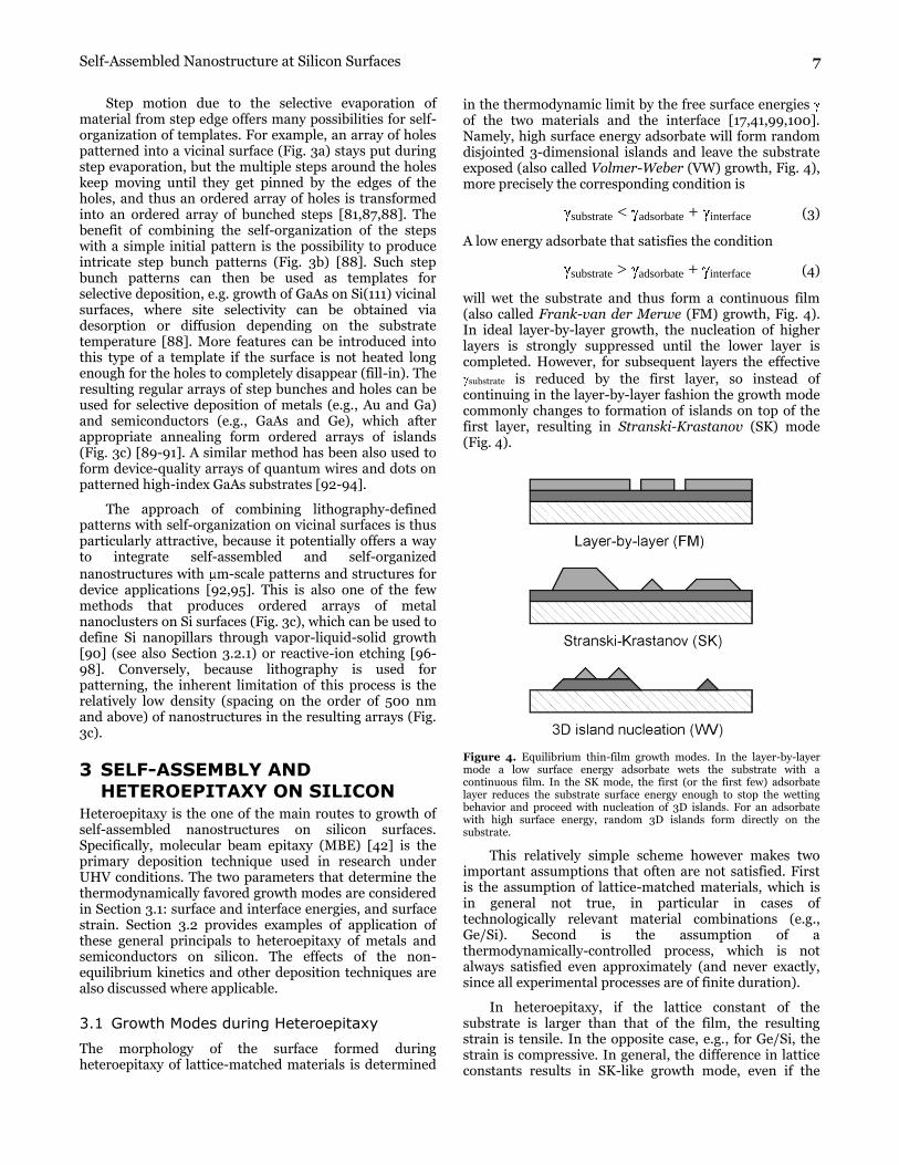
in the thermodynamic limit by the free surface energies of the two materials and the interface [17,41,99,100]. Namely, high surface energy adsorbate will form random disjointed 3-dimensional islands and leave the substrate exposed (also called Volmer-Weber (VW) growth, Fig. 4), more precisely the corresponding condition is
substrate < adsorbate + interface (3)
A low energy adsorbate that satisfies the condition
substrate > adsorbate + interface (4)
will wet the substrate and thus form a continuous film (also called Frank-van der Merwe (FM) growth, Fig. 4). In ideal layer-by-layer growth, the nucleation of higher layers is strongly suppressed until the lower layer is completed. However, for subsequent layers the effective
substrate is reduced by the first layer, so instead of continuing in the layer-by-layer fashion the growth mode commonly changes to formation of islands on top of the first layer, resulting in Stranski-Krastanov (SK) mode (Fig. 4).
Figure 4. Equilibrium thin-film growth modes. In the layer-by-layer mode a low surface energy adsorbate wets the substrate with a continuous film. In the SK mode, the first (or the first few) adsorbate layer reduces the substrate surface energy enough to stop the wetting behavior and proceed with nucleation of 3D islands. For an adsorbate with high surface energy, random 3D islands form directly on the substrate.
This relatively simple scheme however makes two important assumptions that often are not satisfied. First is the assumption of lattice-matched materials, which is in general not true, in particular in cases of technologically relevant material combinations (e.g., Ge/Si). Second is the assumption of a thermodynamically-controlled process, which is not always satisfied even approximately (and never exactly, since all experimental processes are of finite duration).
In heteroepitaxy, if the lattice constant of the substrate is larger than that of the film, the resulting strain is tensile. In the opposite case, e.g., for Ge/Si, the strain is compressive. In general, the difference in lattice constants results in SK-like growth mode, even if the

8 Self-Assembled Nanostructure at Silicon Surfaces
surface energies favor the layer-by-layer growth, because roughening of the growth front allows to relax the elastic strain that otherwise would build up in the film [10,17,41,99]. If this relaxation is not sufficient, plastic strain relief sets in, e.g., creation of misfit dislocations and other defects in the film.
The dominance of kinetic effects vs. thermodynamic stability is largely determined by the deposition flux and substrate temperature during growth. If the diffusion of the deposited atoms allows them to sample multiple bonding configurations, the energetically favored sites become populated with higher probability, and the resulting distribution tends towards the thermodynamically stable structures. If however either diffusion rate or diffusion length is limited, the deposited atoms are likely to be incorporated into the nearest site (typically an island edge) and thus kinetically preferred structures are formed.
While the variability of the growth modes that occurs in real heteroepitaxy was initially seen as an impediment to the smooth film growth required for device-quality materials, it soon became evident that these effects can be used to either enhance the film quality, or to produce self-assembled nanostructures [17,41]. For example, if the flux and substrate temperature during the deposition are adjusted to allow the adsorbate atoms to diffuse to reach the nearest substrate step, the so-called step-flow growth mode is realized, which results in very smooth films, e.g., homoepitaxy of Si under such conditions is routinely used to grow high-quality Si buffer layers. Additional examples of equilibrium and non-equilibrium driven SA in heteroepitaxy on Si are presented throughout Section 3.2.
3.2 Self-Assembly in Strained Heteroepitaxy
Formation of nanoscale islands via SK or VW heteroepitaxial growth is one of the most widely studied forms of self-assembly on a variety of substrates [17]. On silicon, the substrate of choice for microelectronics applications, the deposition of metals (Section 3.2.1) and semiconductors (Sections 3.2.2 and 3.2.3) has been examined for possible SA island formation. For metals, alloys, and semiconductors, both equilibrium and non-equilibrium processes can lead to SA.
3.2.1 Metal and Metal-Semiconductor Heteroepitaxy on Silicon
Metals tend not to form SA nanostructures when deposited directly on silicon, because of silicide formation and surface energy differences [48]. Thus formation of metallic nanostructures on silicon has to be guided by preferential deposition or diffusion on nanostructured and/or passivated surface templates [17,27,101-103], but not by heteroepitaxy-induced strain alone. One notable exception is the growth of several (primarily rare-earth) metal silicide nanowires on Si(001) (Fig. 5) which is driven by the asymmetric mismatch of the respective silicides with the Si lattice constant along orthogonal directions [102,104-106]. The wires are formed in this case, because the growth proceeds uninterrupted along
the direction where the constants match, but is limited in the perpendicular direction. An intriguing property of these wires is that they appear to be stable against atomic step motion during annealing, i.e. moving steps get pinned around the wires, but the wires remain uninterrupted (Fig. 5) [102,106]. While certainly very useful for creating individual long uninterrupted wires, this property however limits the possibilities of using stepped surface templates (Section 4.1) to control self-organization of many of such wires (Section 4.3).
Figure 5. STM image of Ho silicide nanowires on stepped Si(001) surface. Note that multiple substrate steps stretch to accommodate uninterrupted nanowires. Reprinted with permission from Ref. [106], J. Nogami et al., Phys. Rev. B 63, 233305 (2000). © 2001, American Physical Society.
Oxidation of metal films on silicon can result in SA metal-oxide nanostructures, in this case the volume change during the oxidation, rather than the lattice mismatch, is believed to be responsible for the SA process [107,108]. One of the reasons metal oxides have attracted attention is that such SA structures can be magnetic [108] and thus offer a way to combine the benefits of silicon substrates and magnetic devices. SA 3D islands of ferromagnetic metal compounds that are used in semiconductor-based spintronics, e.g., MnAs [109,110], have also been demonstrated on Si(111) with SA achieved via the combination of the lattice mismatch and growth kinetics [110]. More complicated SA schemes are possible, e.g., by metal deposition onto SA structures formed by the Ge/Si heteroepitaxy (Sections 3.2.2-3.2.3) which produces metal-semiconductor compound nanocrystals [111].
ZnO is a metal oxide that has attracted attention for optical device applications, because of the exciton binding energy of 60 meV, i.e., larger than that of wide band gap semiconductors. ZnO SA quantum dots form in VW-like growth mode on silicon surfaces with intermediate layers, e.g., silicon oxide [112] and GaSe bilayer [113]. For potential applications, e.g., room temperature short-wavelength nanolaser arrays, the main interest is in large island densities [114], which have been achieved by the vapor-liquid-solid (VLS) growth [115].

Self-Assembled Nanostructure at Silicon Surfaces 9
Figure 6. Silicon nanowire growth by vapor-liquid-solid epitaxy (VLSE). (a) VLSE schematic. (b) Vertical Si nanowires grown on Si(111) wafer. (c) Three sets of Si nanowires (preferred orientations indicated by arrows) grown on Si(001). Reprinted with permission from Ref. [115], Y. Y. Wu et al., Chem. Eur. J. 8, 1261 (2002). © 2002, Wiley-VCH.
VLS [116] is a general method of growing semiconductor nanostructures [117] and nanowires [115,118,119] using metal nanoparticles as catalysts (Fig. 6a). VLS has been successfully used to grow bulk unsupported Si nanowires [119,120] and oriented Si nanowires on Si surfaces (Fig. 6) [115,121,122]. Free-standing single-crystal nanowires in general do not form during semiconductor heteroepitaxy (Section 3.2.2), because such anisotropic crystals are thermodynamically unstable relative to bulk structures. The primary role of the metal particles is then to kinetically promote the growth of nanowires [115]. Their secondary role is to determine the diameter of the growing nanowires, which can thus be controlled if size-selected metal nanoparticles are used [115,119]. The third possible function of the metal clusters is controlling the position of the resulting nanowires, which becomes meaningful if the clusters themselves can be positioned on a surface. During the VLS growth of Si, the metal (e.g., Au) particles partially melt and form a liquid alloy with the Si substrate. During
the subsequent Si deposition, the liquid becomes a preferential adsorption site and the alloy quickly supersaturates with Si, which leads to Si precipitation and nanowire growth [115]. Silicon nanowires preferentially
grow along the 111 direction, which produces epitaxial nanowires with unique orientation on Si(111) (Fig. 6b)
and nanowires along the three equivalent 111 directions growing on Si(001) (Fig. 6c) [115].
VLS is thus a technique of choice for growing densely-packed arrays of oriented single-crystal self-assembled Si nanowires. The seed metal particles, which terminate the wires, may be beneficial for some applications (e.g., for chemical selectivity), but also result in essentially unavoidable residual metal content—potential disadvantage for applications where high-purity Si is required (e.g., electronics). The self-assembled nanowires produced by VLS are not inherently self-organized (apart from the preferential orientation on epitaxial substrates), but because of its flexibility in terms of materials and conditions, VLS can potentially be combined with other approaches to produce self-organized structures.
3.2.2 Semiconductor Heteroepitaxy on Silicon:
III-Vs and Ge
Semiconductor heteroepitaxy includes the three ―canonical‖ material systems in which SA nanostructures with well-defined shapes and size distributions form under a variety of growth and post-deposition
treatments: Ge/Si ( 4% mismatch), InAs/GaAs ( 7%
mismatch), and InP/GaAs ( 3.8% mismatch) [17]. In addition to the widely studied elemental semiconductor heteropitaxy of Ge/Si discussed below, SA of compound semiconductors on Si surfaces have been attempted as well, with the idea that the large lattice mismatches [123] that prevent smooth film growth in such combinations can result in SA of 3D islands. MBE of GaAs on Si(001) results in formation of SA islands with nucleation and evolution of shapes and sizes similar to those observed in the Ge/Si system, which suggests that a similar mechanism is responsible for SA [124]. High-quality SA GaAs quantum dots can be also produced by ―droplet epitaxy‖ on GaSe-terminated Si(111) surface [125] or As-terminated Si(001) [126], whereby initially nm-size Ga droplets are formed under Ga flux and then they are transformed into GaAs by annealing under As flux [125,126]. InAs is another III-V semiconductor for which the direct MBE growth on Si(001) results in SA quantum dots [127], but a more common method for growing quantum dots of InAs [128,129] and other compound semiconductors [130] is to use H-terminated Si(001) substrates.
As already mentioned, Ge/Si is a prototype for elemental semiconductor heteropitaxy that exhibits self-assembly and self-organization. The system is currently seen as one of the most promising for a variety of device applications, e.g. see Refs. [21,33,131-133]. The extensive body of experimental and theoretical work on Ge/Si epitaxy and nanostructures is covered in several recent reviews [10,21,41,54,134]. In part because they are so

10 Self-Assembled Nanostructure at Silicon Surfaces
widely studied, the mechanisms of SA nanostructures formation and evolution have been very controversial in this system and the debate offers an instructive example of development of the general understanding of the SA process.
Figure 7. Strain relief in the Stranski-Krastanov growth mode. (a) Pseudomorphic wetting layer with tetragonal distortion. (b) Coherently strained 3D islands with steep facets. (c) On a vicinal substrate, faceting of the film through step bunching.
Si and Ge have the same crystal structure, but Ge lattice constant is 4.2% larger, which results in compressive strain when Ge films grow pseudomorphically on Si. First, several uniformly strained full atomic layers of Ge form a wetting layer (Fig. 7a). The thickness of this wetting layer is largely determined by the ability of tetragonal distortion in vertical direction to relieve the strain. Since the lateral compressive strain still accumulates with increasing film thickness, the film becomes unstable against long-wavelength corrugation of the surface, a process particularly pronounced during growth on vicinal substrates (Fig. 7c), whereby ripples with more than 10 times the periodicity of substrate steps develop [41,135]. Note that these structures because of their large periodicity can only contain very shallow facets. When such roughness is not sufficient for strain relief, steeper (higher-index) step bunches are introduced, leading to formation of 3D islands (Fig. 7b) with well-defined facets [10,41].
3.2.3 Ge/Si Island Shapes and Evolution: Kinetics vs. Equilibrium
Similar to the surface roughening with increasing film thickness discussed above, for classification purposes, the shapes of Ge islands on Si(001) (Fig. 8) can be described within the same framework of introducing progressively higher-index (steeper) facets with increasing island size [41,54]. For the smallest islands, {105} facets with 11.30 tilt relative to (001) plane appear. These islands come in two shapes: square-based pyramids, and elongated (in
either 100 or 010 direction) ―huts‖ with two trapezoidal and two triangular sides [41,136]. For larger islands two more facets appear: {113} with 25.20 tilt relative to (001) plane and {518}. The latter was re-assigned as {15 3 23} with 33.60 tilt [137] through comparison to a stable Ge surface [138]. Multifaceted islands with roughly symmetric bases are referred to as ―domes‖ [54,139] and consist mainly of {113} and {15 3 23} facets, but also contain small {105} and (001) facets. Finally, the largest islands are called ―superdomes‖ [54,140], they are similar in shape to domes, but contain {111} and other steeper facets near edges.
Figure 8. STM topograph of strained Ge nanocrystals on Si(001), showing both pyramids and domes. The gray scale is proportional to the
local surface curvature as determined by the Laplacian 2h(x, y): positive curvature is white, flat areas are gray, and negative curvature is black. Reprinted with permission from Ref. [139], G. Medeiros-Ribeiro et al., Science 279, 353 (1998). © 1998, American Association for the Advancement of Science.
Explaining the different island shapes (Fig. 8) and their relative stabilities, in an attempt to derive rational methods of growing SA nanostructures, became one of the most controversial problems in the field of SA systems. The huts were the first Ge/Si island type to be discovered [136], but now they are considered to be only metastable, because in annealing experiments huts transform into pyramids [141]. Pyramids and domes, on the other hand, co-exist (Fig. 8) over a wide range of coverage, temperature, growth and annealing conditions, and thus the growth and shape transition mechanisms of these two island types have been extensively studied and debated for over a decade [10,41,54].
The main issue is whether the observed changes in island shapes are the result of a kinetic roughening process (e.g., Ostwald ripening [142]) or simply an equilibrium distribution, determined by the appropriate island energies. For practical purposes the equilibrium structures are preferred: they inherently evolve towards controlled uniform sizes, potentially can be grown by any deposition method, and are more likely to remain stable over the lifetime of devices (which may be orders of magnitude longer than the duration of the deposition process). If, on the other hand, the island types are determined by growth kinetics, then good understanding of the relative rates of the various processes is indispensable for controlling the appropriate growth parameters and stabilizing the structures (e.g., through surfactants or encapsulation).

Self-Assembled Nanostructure at Silicon Surfaces 11
Observable distinctions between kinetic and equilibrium processes are readily predicted by simple models. Classic Ostwald ripening, for example, leads to strictly unimodal, albeit not very narrow, particle size distribution and the average particle size growing monotonically with time [142]. For equilibrium models, in a system with several competing interactions, the existence of an optimal particle size (and shape) can be expected. Unfortunately, the actual experimental observations for the Ge/Si system are inconsistent with predictions from simple kinetic or equilibrium models. The problem then becomes that of choosing the appropriate model extensions and including additional surface processes, which in general tends to obscure the differences between model predictions. The development of the complex equilibrium models for this system has been extensively covered recently [54,143,144], the somewhat more illustrative example of the kinetics models is briefly discussed below.
The classic Ostwald ripening model and its extensions to 3D crystals on surfaces [53,142,145-148] predict that the chemical potential of an island decreases continuously with size because of the decreasing radius of curvature and surface/volume ratio. The atoms then have a higher probability to detach from smaller islands and to attach to larger ones, thus the larger islands grow at the expense of the smaller ones, which means that the average island size increases with time and the surface number density of islands decreases. The island size distribution on Ge/Si samples with co-existing pyramids and domes remains bimodal during growth and annealing [54,141], so it clearly does not correspond to a simple Ostwald ripening. It has been suggested that a discontinuous change in the chemical potential of an island during its shape transformation could modify Ostwald ripening kinetics to produce a bimodal distribution [149,150]. Quantitatively, the experimental size distribution [149] shows indications of size-limited behavior for both pyramids and domes, and thus narrower than expected width of these distributions. Therefore, an additional island size-dependent term in the adatom attachment rate is required in a kinetic model. Multiple such mechanisms have been suggested [54], e.g., the increased strain for large islands at their edges and in surrounding substrates which favor detachment and flow away from these islands respectively [143].
Realistic equilibrium models [54] also have to include multiple energy terms: bulk strain, facet, interface, and edge energies for individual islands [151,152], as well as inter-island elastic interactions and ensemble thermodynamics [54]. As a result of the multiple terms in both kinetic and equilibrium models, their predictions depend on a number of unknown parameters and thus are difficult to compare to each other and experimental data. Other practical aspects of this system further increase the complexity, to name just two: above 650 °C all Ge islands are only metastable with respect to SiGe alloying [153], and transition shapes exist during growth but disappear upon cooling [137].
The general difficulty in assigning exclusively kinetic or equilibrium character to SA island formation has been noted in comparing growth behavior of Ge/Si, Co/Si, and Co/Ge/Si, where ―in spite of the marked differences in surface thermodynamics and kinetic pathways … remarkably similar nanocrystal arrays‖ have been formed on the surface [111]. The main conclusion from the extensive research on the prototypical Ge/Si heteroepitaxy is that while the structures themselves appear to be thermodynamically stable, their growth is determined as much by kinetic pathways towards the equilibrium, as by the equilibrium configuration itself [54,143,154]. In other words, partially annealed configurations may exhibit strong non-equilibrium features, but with sufficient annealing distributions consistent with equilibrium theories emerge. One possible ―general‖ scenario was suggested in Ref. [143]. Initial island nucleation and 2D-3D transitions are strongly kinetics-dependent. With increasing coverage, strain effects become relevant and island sizes and densities approach equilibrium values, but size-dependent kinetic terms are still significant. As the deposition flux is decreased and stopped, further annealing brings the system close to the equilibrium configuration, including saturated values of island sizes and density.
3.2.4 Ge/Si Multilayers
The ability to form ordered multilayer structures during the Ge/Si heteroepitaxy arises from inter-layer interactions, which are discussed in detail in several excellent specialized reviews [10,41,134]. Here we focus on the importance of the multilayer ordering as a unique self-organization mechanism for self-assembled surface structures. Briefly, during the multilayer Ge/Si heteroepitaxy, nanostructures formed in the preceding layer affect the strain in the subsequent overlayer, which leads to self-alignment of nanostructures between the layers [10,41,135,155]. In fact, these interactions can lead to improved size-uniformity and lateral ordering of the nanodots in the topmost layer even when the first layer was randomly nucleated [10,41]. Almost perfect uniformity and lateral ordering is achieved when the first layer is pre-patterned either artificially [133] or by self-organized template on the substrate [10,41]. The latter cases offer some of the best practical realizations of truly self-organized arrays of self-assembled nanostructures (Section 4.4.2).
4 SELF-ASSEMBLED NANOSTRUCTURES ON VICINAL
SURFACES Vicinal surfaces and atomic steps are intimately related to self-assembly and self-organization on silicon surfaces. First, the vicinal surfaces themselves are subject to SO. Various aspects of these SO processes are described in Section 4.1: vicinal Si(111) and Si(001) used as substrates, formation of regular arrays of single atomic steps, step bunches, and domain boundaries. The traditional 3D heteroepitaxial growth modes are modified by the

12 Self-Assembled Nanostructure at Silicon Surfaces
presence of multiple substrate steps, because in addition
to the respective surface energies , substrate and
adsorbate step energies have to be taken into account (Section 4.2). One of these growth modes, step decoration, based on the preferential adsorbate attachment at steps, provides the most intuitive way of using steps to guide SO (Section 4.3). But additional ordering, in particular in direction along the steps, can be obtained by combining vicinal templates and strained heteroepitaxy, as demonstrated in Section 4.4.
4.1 Vicinal Surfaces as Self-Organized
Templates
Atomic steps are always present on macroscopic surfaces, so it is natural to develop self-organization schemes that benefit from their presence, rather than attempt to eliminate them. For example, step flow growth techniques take advantage of stepped surfaces for smooth film growth. Because atomistic processes in step dynamics can be controlled by macroscopic surface parameters, e.g., wafer miscut angle, temperature, deposition and annealing rate, etc., there are many approaches that lead to self-organized step arrays. Such SO arrays of steps and step bunches represent surface templates macroscopic in one direction (along the steps) and nanoscale in two other directions (step-step separations and step heights).
Figure 9. Pattern formation by twisted wafer bonding. TEM images of (a) a quasi-perfect square array of twist interfacial dislocations at the bonding interface, (b) square array of pure twist dislocations fabricated by wafer bonding with high-precision (0.01°) control of the twist angle. Reprinted with permission from Ref. [156], D. Buttard et al., IEEE J. Quantum Electron. 38, 995 (2002). © 2002, IEEE.
Single crystal silicon wafers with (001) and, to a lesser extent, (111) orientations are widely available for device fabrication and research purposes. Because of the increasingly stringent requirements of the semiconductor industry, production of these wafers is extremely well-controlled in terms of their composition, number of defects, and orientation. Since it is impossible to produce an atomically flat surface across a whole wafer, often it is beneficial to introduce a controlled miscut to produce a more ordered structure. The miscut orientation is usually
defined in terms of its azimuthal (in-plane) and polar (out-of-plane) angle with respect to a low-index plane orientation, e.g., [001] or [111]. Nominally (001) and (111) substrates are often randomly misoriented by about 0.5°
in both and ; accuracy in both angles of 0.1° and better is possible for customized substrates. Perhaps some of the best evidence for the ultimate wafer-scale control of the miscut and wafer orientation comes from recent advances
in pattern formation by twisted wafer bonding (Fig. 9), with regular nanoscale patterns demonstrated over macroscopic areas [156,157].
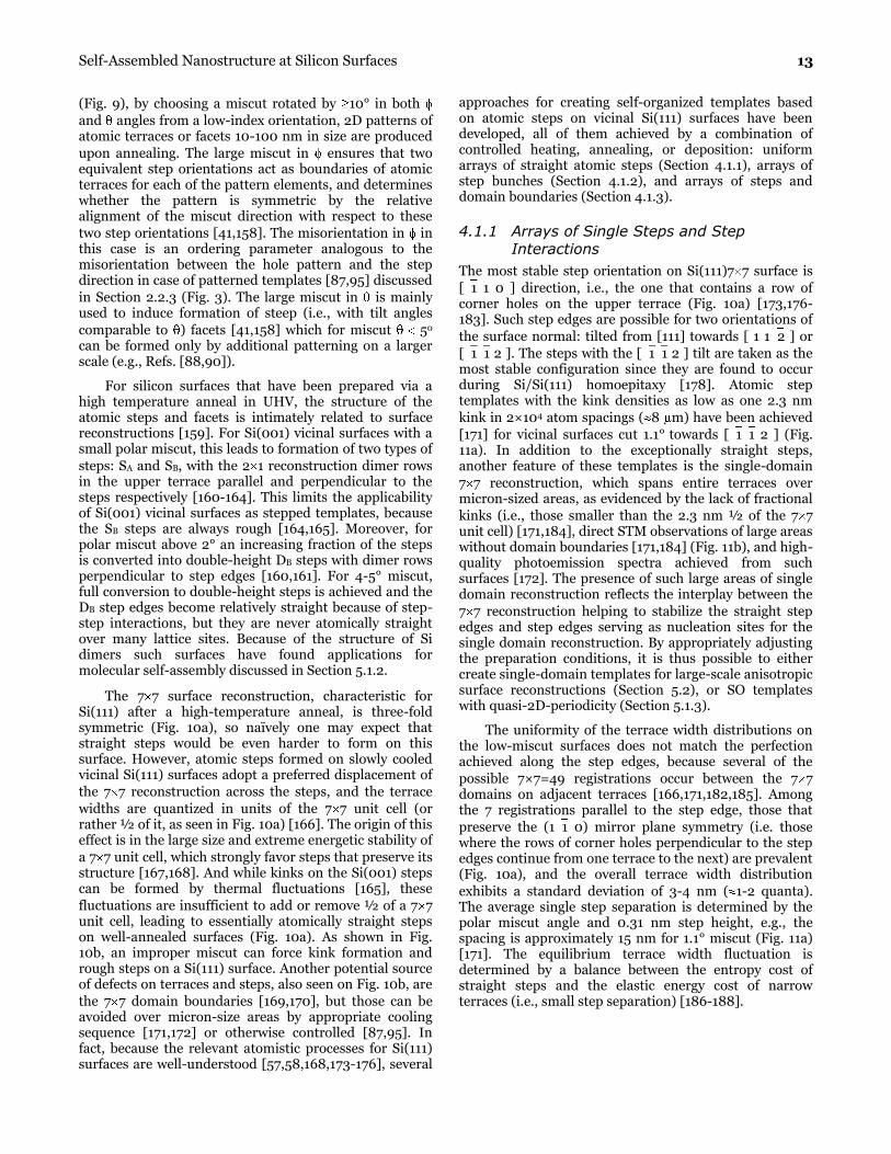
Figure 10. Atomic steps and 7×7 reconstruction on Si(111). (a) Atomically straight step edges (thick dark lines) incorporate rows of 7×7 corner holes. The faint lines parallel to the step edges emphasize the terrace width quantization in units of half a 7×7 unit cell (2.3 nm). (b) Three types of defects for a step array on Si(111): irregular step bunches, kinks along single steps, and 7×7 domain boundaries (jog in the black line). Downhill is to the right. The derivative of the STM topography is used to emphasize the reconstruction and steps in (a) and (b). Adapted in part with permission from Ref. [171], J. Viernow et al., Appl. Phys. Lett. 72, 948 (1998). © 1998, American Institute of Physics.
Steps are inherently linear objects, and thus the obvious goal for SO stepped templates is creation of uniform arrays of straight steps. While control of lateral ordering of SA nanostructures is possible even with straight steps (as discussed in Section 4.4.1), templates with 2D patterns are the most direct way to achieve lateral ordering. Similarly to the wafer bonding example
Self-Assembled Nanostructure at Silicon Surfaces 13
(Fig. 9), by choosing a miscut rotated by 10° in both
and angles from a low-index orientation, 2D patterns of atomic terraces or facets 10-100 nm in size are produced
upon annealing. The large miscut in ensures that two equivalent step orientations act as boundaries of atomic terraces for each of the pattern elements, and determines whether the pattern is symmetric by the relative alignment of the miscut direction with respect to these
two step orientations [41,158]. The misorientation in in this case is an ordering parameter analogous to the misorientation between the hole pattern and the step direction in case of patterned templates [87,95] discussed
in Section 2.2.3 (Fig. 3). The large miscut in is mainly used to induce formation of steep (i.e., with tilt angles
comparable to ) facets [41,158] which for miscut 50 can be formed only by additional patterning on a larger scale (e.g., Refs. [88,90]).
For silicon surfaces that have been prepared via a high temperature anneal in UHV, the structure of the atomic steps and facets is intimately related to surface reconstructions [159]. For Si(001) vicinal surfaces with a small polar miscut, this leads to formation of two types of
steps: SA and SB, with the 2 1 reconstruction dimer rows in the upper terrace parallel and perpendicular to the steps respectively [160-164]. This limits the applicability of Si(001) vicinal surfaces as stepped templates, because the SB steps are always rough [164,165]. Moreover, for polar miscut above 2° an increasing fraction of the steps is converted into double-height DB steps with dimer rows perpendicular to step edges [160,161]. For 4-5° miscut, full conversion to double-height steps is achieved and the DB step edges become relatively straight because of step-step interactions, but they are never atomically straight over many lattice sites. Because of the structure of Si dimers such surfaces have found applications for molecular self-assembly discussed in Section 5.1.2.
The 7 7 surface reconstruction, characteristic for Si(111) after a high-temperature anneal, is three-fold symmetric (Fig. 10a), so naïvely one may expect that straight steps would be even harder to form on this surface. However, atomic steps formed on slowly cooled vicinal Si(111) surfaces adopt a preferred displacement of
the 7 7 reconstruction across the steps, and the terrace
widths are quantized in units of the 7 7 unit cell (or rather ½ of it, as seen in Fig. 10a) [166]. The origin of this effect is in the large size and extreme energetic stability of
a 7 7 unit cell, which strongly favor steps that preserve its structure [167,168]. And while kinks on the Si(001) steps can be formed by thermal fluctuations [165], these
fluctuations are insufficient to add or remove ½ of a 7 7 unit cell, leading to essentially atomically straight steps on well-annealed surfaces (Fig. 10a). As shown in Fig. 10b, an improper miscut can force kink formation and rough steps on a Si(111) surface. Another potential source of defects on terraces and steps, also seen on Fig. 10b, are
the 7 7 domain boundaries [169,170], but those can be avoided over micron-size areas by appropriate cooling sequence [171,172] or otherwise controlled [87,95]. In fact, because the relevant atomistic processes for Si(111) surfaces are well-understood [57,58,168,173-176], several
approaches for creating self-organized templates based on atomic steps on vicinal Si(111) surfaces have been developed, all of them achieved by a combination of controlled heating, annealing, or deposition: uniform arrays of straight atomic steps (Section 4.1.1), arrays of step bunches (Section 4.1.2), and arrays of steps and domain boundaries (Section 4.1.3).
4.1.1 Arrays of Single Steps and Step
Interactions
The most stable step orientation on Si(111)7 7 surface is
[ 1 1 0 ] direction, i.e., the one that contains a row of corner holes on the upper terrace (Fig. 10a) [173,176-183]. Such step edges are possible for two orientations of
the surface normal: tilted from [111] towards [ 1 1 2 ] or
[ 1 1 2 ]. The steps with the [ 1 1 2 ] tilt are taken as the most stable configuration since they are found to occur during Si/Si(111) homoepitaxy [178]. Atomic step templates with the kink densities as low as one 2.3 nm
kink in 2×10⁴ atom spacings ( 8 m) have been achieved
[171] for vicinal surfaces cut 1.1° towards [ 1 1 2 ] (Fig. 11a). In addition to the exceptionally straight steps, another feature of these templates is the single-domain
7 7 reconstruction, which spans entire terraces over micron-sized areas, as evidenced by the lack of fractional
kinks (i.e., those smaller than the 2.3 nm ½ of the 7 7 unit cell) [171,184], direct STM observations of large areas without domain boundaries [171,184] (Fig. 11b), and high-quality photoemission spectra achieved from such surfaces [172]. The presence of such large areas of single domain reconstruction reflects the interplay between the
7 7 reconstruction helping to stabilize the straight step edges and step edges serving as nucleation sites for the single domain reconstruction. By appropriately adjusting the preparation conditions, it is thus possible to either create single-domain templates for large-scale anisotropic surface reconstructions (Section 5.2), or SO templates with quasi-2D-periodicity (Section 5.1.3).
The uniformity of the terrace width distributions on the low-miscut surfaces does not match the perfection achieved along the step edges, because several of the
possible 7×7=49 registrations occur between the 7 7 domains on adjacent terraces [166,171,182,185]. Among the 7 registrations parallel to the step edge, those that
preserve the (1 1 0) mirror plane symmetry (i.e. those where the rows of corner holes perpendicular to the step edges continue from one terrace to the next) are prevalent (Fig. 10a), and the overall terrace width distribution
exhibits a standard deviation of 3-4 nm ( 1-2 quanta). The average single step separation is determined by the polar miscut angle and 0.31 nm step height, e.g., the spacing is approximately 15 nm for 1.1° miscut (Fig. 11a) [171]. The equilibrium terrace width fluctuation is determined by a balance between the entropy cost of straight steps and the elastic energy cost of narrow terraces (i.e., small step separation) [186-188].

14 Self-Assembled Nanostructure at Silicon Surfaces
Figure 11. Arrays of single steps on Si(111). (a) Three-dimensional view of a high-quality array of single steps (0.3 nm height) prepared on Si(111)
miscut by 1.1° towards the [ 1 1 2] direction. There is only one kink (arrow) in the 340×340 nm2 area, the rest of the steps are atomically straight [171]. The vertical scale is enhanced by a factor of 20. (b) Faint traces of the 7×7 reconstruction pattern and the absence of kinks in this STM topography derivative image indicate that the 7×7 reconstruction is single-domain over the entire image.
Elastic interactions between steps can be generalized according to their symmetry into monopole and dipole character. The monopole term originates from the presence of elastic-stress domains on reconstructed surfaces, on vicinal surfaces atomic steps act as domain walls and the corresponding domain-wall energy has a logarithmic dependence on their separation l [189]. The elastic-dipole interaction between steps arises to compensate for the non-zero moment of the surface capillary forces acting on upper and lower terraces (Fig. 12). The dipole interaction thus can have components perpendicular or parallel to the substrate (Fig. 12) and its energy has l-2 dependence [190,191]. The dipole interaction is repulsive for steps of the same sign (i.e. the same downhill direction), so it helps stabilize step arrays on vicinal surfaces. The terrace width distribution on vicinal Si(111) surfaces is predominantly determined by the dipole interactions between steps [186]. Note that the dipole interaction can be attractive in cases where materials with different elastic constants are involved,
e.g., adsorbate islands can be either attracted, or repelled by the steps. When both the monopole and dipole interactions are included, one has to add to the total energy an attractive cross-term with a l-1 dependence [192,193]. The combination of these elastic interactions is responsible, for example, for the minority terrace width distribution on vicinal Si(001) surfaces [194].
Figure 12. Surface capillary forces acting on the upper and lower terraces produce non-zero moment acting on the step, with components perpendicular and parallel to the surface.
For polar miscut of 1-20 long-range dipole repulsion stabilizes arrays of individual steps on both Si(001) and Si(111). The equilibrium terrace width fluctuations are determined for Si(001) and Si(111) primarily by the monopole and dipole terms respectively with fluctuations proportional correspondingly to l½ and l [187,188]. Smaller step separation l is thus expected to produce increasingly straight steps, but the resulting larger miscut angles often produce step bunching. On Si(001), as discussed earlier, step doubling produces the DB steps with dimer rows perpendicular to step edges [160,161] and in this configuration formation of individual kinks is difficult to suppress over multiple dimer sites. Si(111) steps become unstable against formation of triple-steps [176] for polar miscut angles larger than about 2°. An isolated triple-height step is energetically unfavorable compared to 3 single steps, but with decreasing step spacing the elastic-dipole repulsion increases, and the total energy cost can be lowered by forming the triple-steps (with correspondingly larger spacing) [186].
4.1.2 Step Bunches and Facets
Just as for single steps, vicinal surfaces with miscut
towards [1 1 2] or [ 1 1 2 ] directions produce better ordered step bunches [184,195] than other vicinal surfaces [58,196-198]. In particular, on surfaces with
polar miscut towards [1 1 2], periodic arrays of (111) terraces and high-density facets are formed [184,195]. Periodicity of these step arrays is independent of the miscut angle up to 6°, but the width of the stepped facets increases with the miscut [184,195], which in principle should allow to create arbitrary ratios of the flat and stepped regions by adjusting the miscut angle (Fig. 13). Both the perfection and constant periodicity are attributed to the exceptionally stable structure of the facet that forms, which is characterized by an average facet angle of 12.7° [195] and is composed of narrow ledges
with reconstructions similar to the 5 5 analog of the 7 7 reconstruction [184,195]. It is important to note that because of the large width of the flat terraces and thus

Self-Assembled Nanostructure at Silicon Surfaces 15
significantly reduced step interactions, formation of the regular arrays of bunched steps is much slower than that of the single-steps [184].
Figure 13. Arrays of step bunches on vicinal Si(111). (a) There are two parameters for uniform arrays of step bunches: the periodicity L defined
by the polar miscut angle , and the terrace width (L – l) defined by the
facet angle of the bunches. For Si(111) miscut towards the [ 2 1 1 ] direction the periodicity and the stable facet angle remain constant for
<6°, therefore the terrace width systematically decreases in the miscut series of 1°, 2°, 4°, and 6° (b-e). The derivative of the STM topography is shown to emphasize the stepped regions. Downhill is to the right. Adapted in part with permission from Ref. [195], F. K. Men et al., Phys. Rev. Lett. 88, 096105 (2002). © 2002, American Physical Society.
Figure 14. Silicon crystal lattice between (001) and (111) orientations. Single unit cells of bulk-terminated orientations are marked with solid circles. After Ref. [159], A. A. Baski et al., Surf. Sci. 392, 69 (1997). © 1997, Elsevier Science.
The bunched step facets are energetically stable, but the step edge perfection of the single steps is lost during their formation. In the range of miscut angles between the (111) and (001) the evolution of stable structures is characterized by several stable planes: (5 5 12), (113), (114), (118), (331), and mixtures of various facets in between [158,159,196,199-201]. Thus, in general, the local structural perfection is recovered at large miscut angles, but not the long-range periodicity of the steps.
Figure 15. Atomically accurate Si grating. A series of steps with the perfect periodicity of 17 atomic rows (5.73 nm) for Si(557). STM image of the x derivative of the topography and cross-sectional profiles averaged over the y axis. Adapted with permission from Ref. [202], A. Kirakosian et al., Appl. Phys. Lett. 79, 1608 (2001). © 2001, American Institute of Physics.
There is however a number of vicinal Si(111) and Si(001) surfaces that lend themselves for use as self-organized templates (Fig. 14). In particularly with Au as an adsorbate [58], a large fraction of the possible orientations has actually produced well-ordered structures, and many other possible crystallographic orientations have yet to be explored. Electronic properties of these surfaces are described in Section 5.2. In terms of its structure, perhaps the simplest is the case of a vicinal
surface with 9.45° miscut towards [ 1 1 2 ] direction. It is composed of steps separated by (111) terraces that
accommodate a single row of the 7 7 reconstruction and one additional string of Si adatoms (Fig. 15) [202]. This is an example of a self-assembled atomically-precise grating with the largest corrugation and unit cell achieved on Si surfaces [202]. The periodicity of this structure is expressed in terms of the Si lattice constant – one of the best-known lattice parameters, which suggests possible applications for nanoscale metrology [203,204]. Atomically-precise nature of this template also allows to create ordered atomic structures over at least hundreds of nanometers (Section 5.2.2).
4.1.3 Steps and Domain Boundaries
Stepped templates, discussed in the previous two sub-sections, took advantage of the near-equilibrium step structures, achieved through high-temperature annealing
and stabilized by the 7 7 reconstruction or its analogs. Another well-studied process on silicon surfaces is the
behavior and structure of steps and 7 7 domains during homoepitaxial growth [205-209], which is generally a non-equilibrium process, but can also result in ordered structures. Similarly to the annealing case, the ordering can be guided either by pre-patterning the surface, or by controlling the deposition conditions.
On lithographically-patterned elongated mesas
oriented parallel to [1 1 2] direction, step flow growth results in terraces with stable steps along the two
symmetric 211 directions, and under appropriate conditions dense and rather regular step arrays are formed (Fig. 16) [59,210].
As discussed in Section 4.1.1, to produce atomically straight single steps, it was important to achieve
equilibrated single-domain 7 7 reconstruction over

16 Self-Assembled Nanostructure at Silicon Surfaces
entire terraces (Figs. 10-11) [171,184]. An alternative approach to step ordering is to allow random nucleation
and growth of the 7 7 domains at multiple sites near the step edges. Because of the large unit cell, registration between random domains is unlikely, so when such domains collide, out-of-phase boundaries (OPBs) are formed [87]. Thus a 2D quasi-periodic network of atomic steps and OPBs is formed [87,95], with the periodicities
determined by step separation and 7 7 domain nucleation conditions. The uniformity of these networks can be dramatically improved by depositing additional Si. During Si homoepitaxy, atoms preferentially are incorporated at cross-points of OPBs and steps, and combined with fluctuations of the growth rate this results in wavy growth fronts, with the periodicity of the waviness determined by the growth conditions. During such growth, the area of smaller domains tends to diminish, until they merge with larger neighbors, and thus a considerably more uniform network of steps and OPBs is formed [87,95].
Figure 16. Uniform step array on a mesa top surface. Schematic view and an AFM image of an array produced by step-flow growth. Reprinted with permission from Ref. [59], T. Ogino et al., Surf. Sci. 514, 1 (2002). © 2002, Elsevier Science.
4.2 Heteroepitaxy in 2D
The step flow growth is an example of a 2D equivalent of the layer-by-layer growth in 3D. The other 3D growth processes can also be generalized for cases of submonolayer deposition on stepped surfaces, where essentially 2D growth occurs [17,41]. Instead of the
surface free energies however, one has to consider a set
of respective step energies : substrate steps ( substrate),
adsorbate island edges ( adsorbate) and the interface between a substrate step and an island attached to it
( interface). Replacing ‗s with ‗s in Eq. 3 for 3D growth, we get a set of conditions for the adsorbate to form disjointed islands along steps
substrate < adsorbate + interface (5)
For continuous adsorbate stripes attached to substrate steps
substrate > adsorbate + interface (6)
The familiar equilibrium growth modes that re-appear in a 2D world can be classified as row-by-row, Stranski-Krastanov, and island growth in analogy with the 3D equivalents (Fig. 17). A new possibility arises if the following condition is satisfied
interface > adsorbate + substrate (7)
in which case adsorbate islands will form, but avoid the step (Fig. 17). This is a uniquely 2D phenomenon, since in 3D growth this would correspond to adsorbate islands floating above the substrate.
Figure 17. Equilibrium growth modes at steps. The first three regimes (left-to-right) are essentially 2D equivalents of the classic equilibrium growth modes—compare to Fig. 4. The step energy rather than the surface free energy is the parameter responsible for the different growth modes in the 2D case. The last regime, with islands not attached to steps is a uniquely 2D phenomenon (3D equivalent would be islands floating above the substrate surface).
In 2D growth just like in the 3D case, the general rule is to use low deposition flux and sufficiently high substrate temperature to approach the equilibrium distributions in experimentally observed growth modes. The next two sections discuss examples of the use of the different 3D and 2D growth phenomena in self-assembly and self-organization of nanostructures on Si surfaces.
4.3 Step Decoration & Self-Assembled
Nanowires
Step decoration takes advantage of preferential attachment and/or growth of the deposited material at the atomic steps. The technique has been pioneered almost half-a-century ago when it was used to visualize atomic-height steps on cleavage surfaces of sodium chloride by decorating them with gold [211]. Step selectivity of various surface processes can be utilized to produce step-decoration, e.g., for silver on graphite step decoration can be achieved through: selective nanocluster growth [212], diffusion [212-214], and nanowire growth by electrochemistry [215,216]. For epitaxial systems, step-flow growth results in nanowires of the adsorbate material attached to lower step edges of the substrate (Fig. 17). This growth mode has been first realized for the GaAs/GaAlAs system [217,218], aided by the almost perfect chemical and structural match between these materials.
The step flow growth of self-assembled nanowires can also be achieved for metal-on-metal combinations, if a substrate with high surface energy (e.g., W, Mo) and an adsorbate with low surface energy (e.g., Cu) that does not alloy with the substrate are used [219-225]. STM imaging with elemental contrast through spectroscopic states [222,224,226] allowed to observe the structure of these metal nanowires with atomic resolution and study the corresponding growth modes [103]. Quantitative analysis of thus obtained nanowire width distributions produced two results important for rational size-control of SA nanowires: equilibrium structures exhibit the narrowest size distribution and the lower limit on such distribution is imposed by the roughness of substrate steps [103,227].

Self-Assembled Nanostructure at Silicon Surfaces 17
Step arrays of vicinal Si(111) [171,184] discussed in Section 4.1.1 thus represent an ideal substrate for self-assembly by step decoration because they provide atomically straight steps and essentially single-domain
Si(111)7 7 terraces (Fig. 11)—both factors beneficial for producing self-assembled nanowires with narrow width distribution. Two material combinations have been primarily explored for step decoration on vicinal silicon surfaces: insulator-on-semiconductor CaF2/Si [27,103] and semiconductor-on-semiconductor Ge/Si [10,41]. CaF2/Si(111) is an excellent model system for studies of submonolayer growth and exploring structures and interactions in the <10 nm range, because of the combination of the high-quality vicinal templates and atomically-sharp interfaces. Ge/Si combination produces superior multilayer systems on a larger (> 100 nm) lateral scale and, because inherently conducting SiGe structures are created in the process, it is better suited for characterization by optical and conductivity measurements, including looking for signatures of electron confinement at low temperatures.
4.3.1 CaF2 Nanostripes on Vicinal Silicon
Surfaces
CaF2/Si(111) is a material combination that has been studied for nearly two decades both as a model heteroepitaxial system and as a possible device platform. For devices, it offers a possibility of epitaxial semiconductor-insulator-semiconductor and metal-insulator-semiconductor structures [228-230]. Model studies of growth modes in 2D heteroepitaxy [103,231-236] also benefit from the nearly lattice-matched CaF2/Si(111) combination that forms high-quality epitaxial films and atomically-sharp interfaces [228]. CaF2/Si(001) combination has not been as widely studied [237-240], but step decoration has been recently reported for this system as well [240].
Two types of CaF2/Si(111) interfaces exist: a F-terminated interface at temperatures below 700 °C, and a Ca-terminated interface from 700 °C to the desorption of CaF2 at 800 °C (for a monolayer (ML) coverage). A significant fraction of the interface remains F-terminated on a stepped surface, even at high annealing temperatures [241-243]. The F-terminated interface preserves the orientation of the Si(111) substrate (type A epitaxy) while the Ca-terminated interface rotates the structure azimuthally by 180° (type B epitaxy) [244-249]. The differences in band gaps and band alignment between the clean Si substrate and the two types of interfaces [250,251] allow to positively identify the different types of structures, even on surfaces with complex topography, via the chemical imaging STM mode [234,252].
Figure 18. Non-equilibrium CaF2 growth modes at Si(111) steps. (a) At
550 °C the diffusion length is 7 nm, i.e., less than half the average terrace width, resulting in diffusion-limited growth. Small islands preferentially attach to steps, but also randomly nucleate on terraces. (b) At 600 °C the diffusion length of 8-9 nm allows step-flow growth on most terraces, except the widest ones where not all the CaF2 molecules can reach the step. STM images 100×60 nm2, downhill is to the right, CaF2 appears bright, Si—dark. Adapted in part with permission from Ref. [234], D. Y. Petrovykh et al., J. Vac. Sci. Technol. A 17, 1415 (1999). © 1999, American Vacuum Society.
In general, one would expect a transition from island nucleation to step flow growth with decreasing supersaturation, that is, increasing temperature, decreasing deposition rate, and decreasing step spacing. The results presented in Fig. 18 are consistent with such transition: low temperature (550 °C) and low coverage result in randomly distributed small islands (Fig. 18a), higher temperature (600 °C) and coverage result in apparent step-flow growth (Fig. 18b). The distribution of the small CaF2 islands across terraces in Fig. 18a indicates that there is preferential attachment of CaF2 islands at lower step edges, and a weak repulsion from upper steps

18 Self-Assembled Nanostructure at Silicon Surfaces
edges [234], both factors beneficial for step-flow growth. The presence of residual islands on wider terraces in Fig. 18b suggests that the higher deposition temperature corresponds to CaF2 diffusion length of about 8-9 nm. The CaF2 stripes in Fig. 18b then are far from equilibrium even at 600 °C, which explains the substantial edge
roughness. Interface conversion and Ca/Si(111)3 1 formation [228,253] prevent deposition at temperatures above 650 °C for step-flow-like growth, so smooth CaF2 stripes can not be achieved on Si(111) via a standard step decoration approach. Moreover, as explained in the next section, the initial stages of growth in this system on vicinal surfaces with step separation <15 nm are strongly affected by the presence of the steps.
Figure 19. Reverse step flow growth for CaF2 on Si(111) at high
temperature (830 °C post-anneal). Continuous CaF2 stripes 7 nm wide start at the upper step edge and propagate in the uphill direction. This unusual growth mode is caused by a reversal in stacking at the interface, which causes a lateral incompatibility in the structure across a step. This prevents step flow and ensures that adjacent stripes strictly avoid each other. The derivative of the STM topography is shown to emphasize the steps and stripe edges. Downhill is to the right. Adapted with permission from Ref. [254], J. Viernow et al., Appl. Phys. Lett. 74, 2125 (1999). © 1999, American Institute of Physics.
Smooth CaF2 stripes can however be grown via a process that takes advantage of the interface conversion. Deposition of 1.5 ML of CaF2 followed by a post-anneal at 830 °C establishes a complete layer of Ca-terminated structure with CaF2 stripes on top (Fig. 19) [27,103,234,254]. Note that the stripes are located at upper rather than lower step edges, in fact, they avoid the lower edge to such an extent, that even for coverage very
close to 2 ML an uninterrupted gap is maintained [234,254]. This apparent repulsion is due to the 180° azimuthal rotation introduced into the CaF2 film at the Ca-terminated interface [246] and the resulting mismatch in the orientation if Si steps and CaF2 in the second layer (see diagram in Fig. 19) [234,236,254].
The stripe-and-trench CaF2/Si(111) structure in Fig. 19 is in fact very advantageous as a template for selective deposition, because the periodicity and the width of the trenches can be independently controlled by adjusting the miscut and the coverage respectively. The stripes and trenches are too narrow for selective decoration by metals via direct deposition [255] or electron-stimulated desorption [256] that have been used for CaF2 surfaces. Organic molecules [257] including chemical vapor deposition (CVD) precursors [258] can however be selectively deposited into the trenches due to their higher reactivity (Section 5), and thus Fe nanowires have been successfully grown on such templates via selective CVD [259]. The combination of the well-controlled self-assembled template and the widely applicable selective CVD deposition make this approach promising for growing other types of self-assembled metal nanowires with width and periodicity <20 nm [14,27,103].
4.3.2 Step Decoration in Ge/Si Heteroepitaxy
In Ge/Si heteroepitaxy, most of the step-decoration research has been focused on growth using vicinal Si(001) substrates and primarily on multi-layer structures [10,41]. For submonolayer deposition of Ge, agglomeration at atomic steps has been demonstrated [260] and attributed to step-flow growth, lower step energy for Ge, and enhanced relaxation of Ge-Si lattice mismatch at steps [10]. Deposition of SiGe/Si multilayers on vicinal Si(001) results in self-organized arrays of self-assembled SiGe nanowires [261], the process driven by local strain relaxation [135,262-264]. The nanowire-like structures within each SiGe layer are formed by thickness
undulations within the 5 nm thick layer with about 100 nm periodicity (Fig. 20) [261]. The facets of these wires are defined by Si and SiGe step bunches, thus the structural confinement of the individual wires can be improved by using templates with stronger bunching, such as Si(113) [261,265]. The width and periodicity of these structures (intrinsic characteristics of the bunched Si(001) and Si(113) templates) is larger than those achievable for the CaF2/Si(111) system discussed above. The larger size and the multilayer nature of the samples make conductivity measurements possible for this system, and the resistivity exhibits strong anisotropy (perpendicular vs. parallel to the wires) for these samples at temperature <100 K [10].
For Ge/Si(111) material combination, nanowires have been demonstrated on a Si(111) substrate miscut 0.5°
towards [ 1 1 0 ], i.e., direction perpendicular to that discussed in Section 4.1.1. The template thus consisted of
atomic steps with 110 nm periodicity, and the nanowires with 4.5 nm average height and 43.4 nm average width formed on upper step edges [266,267]. The material distribution in these wires appeared to be nonuniform,

Self-Assembled Nanostructure at Silicon Surfaces 19
which together with the upper step position rules out step-flow as the possible growth mode. The suggested mechanism included initial formation of SA Ge dots on top of a wetting layer (i.e., SK growth mode), with the dots migrating towards upper step edges for strain relaxation. The wires were then completed by additional Ge migration into the gaps between the dots during the subsequent deposition [266,267].
Figure 20. Self-organized arrays of self-assembled SiGe nanowires. A cross-sectional TEM image of SiGe faceted nanowires grown on vicinal Si(113) is shown. The wire stacking changes within the SiGe/Si multilayer between the central (a) and top (b) regions. Reprinted with permission from Ref. [261], K. Brunner et al., Physica E 7, 881 (2000). © 2000, Elsevier Science.
4.4 Strain and Steps—2-dimensional Control of Self-Assembly
To the extent that the two can be separated, the effects of surface strain and steps on heteroepitaxial growth modes have been separately considered in Sections 3.2 and 4.3 respectively. In general, strain provides a very useful mechanism for self-assembly of nanostructures with uniform size and shape distributions, while stepped templates are very effective in ordering structures over macroscopic areas. Here we demonstrate how the combination of the two approaches can result in systems of self-assembled nanostructures that also exhibit 2D self-organized ordering, using examples from the two systems introduced in the previous section: CaF2/Si and Ge/Si. The 2D growth phenomena described for these prototype systems are quite general, as similar growth patterns are also observed in strained heteroepitaxy of III-V semiconductors [268-270].
4.4.1 CaF2/Si(111) Quantum Platelets and
Novel 2D Growth Mode
For the CaF2/Si system the possibility of unusual 2D growth modes is indicated by growth patterns such as shown in Fig. 21. The equilibrium growth modes determined by the step energies alone (Section 4.2) would predict that the adsorbate must preferentially either wet the steps or form a broken interface, but not both simultaneously! Specifically for CaF2/Si(111) combination, complete wetting (e.g., Fig. 21 left) is expected, because the surface energy of Si is almost three
times higher than that of CaF2 [228]. Clearly, some additional factor plays a significant role during heteroepitaxial growth on a vicinal surface.
Figure 21. Step wetting and de-wetting behavior for Si(111) + CaF2. Equilibrium growth predicts either wetting or de-wetting growth at steps, depending on the step and interface energies (Fig. 17). Elastic interactions in the CaF2/Si(111) system however are strong enough to modify the equilibrium behavior, and realize both wetting and de-wetting growth depending on the coverage and step spacing [234,254,271].
As discussed in Section 3.2, strain often determines shapes and sizes of self-assembled nanostructures in heteroepitaxial systems, the elastic energy should then be also considered for an array of SA islands at steps [271]. Two model parameters describe strained islands on a vicinal surface and set the scales of interactions: terrace width W and optimal island size L0. The terrace width is determined by the miscut of a sample and can be controlled in practice within a wide range of values (Section 4.1.1). The optimal size L0 for an isolated strained island is determined by the balance of decreasing edge/area ratio and increasing strain energy with increasing island size, in practice L0 is related to the lattice mismatch during heteroepitaxy [271,272]. An accurate, albeit simple, estimate of L0 is given by the size of a structure over which a mismatch of more than one lattice constant is accrued. For example, for a 2% mismatch typical under CaF2/Si growth conditions [228],
it is about 50 atoms ( 15 nm) in good agreement with the size of isolated islands observed in the CaF2/Si(111) system. Other elastic interactions in the system, e.g., edge/step repulsion, also would typically have a characteristic scale on the order of L0, since the scales are related to the same set of substrate and adsorbate elastic parameters. The L0/W ratio determines the growth mode for systems where strain energy dominates over step energies [271].
For the CaF2/Si(111) system in Figs. 21-22 the optimal island size L0 is on the order of the terrace width W, i.e., the interactions of island edges with substrate steps are strong even for low coverage. Islands attached
to steps then initially grow to reach the width of ½W, to minimize the repulsion between their free edges and both
neighboring steps, and near-optimal length L0 along steps (Fig. 22a). This apparent non-wetting behavior is the result of strain, rather than high step energy of the islands. With increasing coverage, islands grow along the steps but maintain near-constant width, because the edge-step repulsion dominates over intra- and inter-island elastic energy gain. Only when a complete stripe is formed at a step, the free edge begins to advance towards

20 Self-Assembled Nanostructure at Silicon Surfaces
the upper step edge, and the growth appears to be in step-flow mode with increasing coverage (Fig. 22b).
Figure 22. Island-to-stripe transition at a critical coverage. A drastic change in the CaF2 growth mode is observed for 1.1° miscut Si(111) between 0.23 and 0.40 ML coverage. The growth front morphology changes from short islands (black) to long stripes (gray). The observed rough-to-smooth growth front transition is a feature unique to 2D
growth. Such a critical coverage C is predicted by a model that considers the effect of elastic interactions and step energies on the growth front morphology [271].
The rough-to-continuous interface transition is remarkably sharp in this system: there is less than 0.2 ML difference in coverage between the broken and continuous stripe configurations (Fig. 22). The ―reverse SK mode‖ is also a strictly 2D growth phenomenon, since in 3D initially rough growth interfaces do not subsequently become smoother. The qualitative difference between the 2D and 3D growth modes that produces the novel behavior is the fact that in two dimensions the growth proceeds at multiple growth fronts simultaneously, whereas in three dimensions multilayers are grown sequentially. Both of the growth regimes can be potentially useful for forming continuous stripes (Figs. 21 left and 22b) and nanodots (Fig. 21 right) respectively. In the latter case, by properly adjusting the deposition parameters arrays of CaF2 nanodots can be produced with density on the order of 3×1011 cm-2 = 2 Teradots/in2 and fairly uniform size distribution (Fig. 21 right) [234,254].
4.4.2 Self-Organized Lateral Ordering of Ge/Si Nanostructures
Finding the right substrate was the major part of fulfilling the quest for self-organized 2D-ordered arrays of uniform Ge quantum dots. The search began with direct deposition of Ge on vicinal Si substrates with orientations previously used to grow SA Ge islands. On vicinal Si(113)
this resulted in Ge dots aligned primarily at large (>12 ML) step bunches [261,265]. The island formation was attributed to enhanced island nucleation at large Si step bunches, and higher strain produced Ge islands, rather than wires seen in partially relaxed SiGe growth (Section 4.3.2) [261]. Adjacent islands remained separated by narrow gaps in all cases, although there appeared to be a small amount of Ge accumulated in these gaps [265]. There was no correlation of island nucleation across terraces, most likely because the island size (80 nm) was much smaller then the terrace size (>300 nm) [261].
Similar results have been obtained for Ge growth on
Si(001) miscut 4° towards [110], where Ge islands 100
nm in diameter formed at step bunches separating 360 nm (001) terraces [273]. In this case islands also showed no correlation across terraces and maintained separation along the steps, but whereas on the vicinal Si(113) islands appeared to be nucleating on the bunched steps [261], for vicinal Si(001) the islands were not as well aligned along the bunches, and upper side of (001) facets was determined to be the preferential nucleation site [273]. The same Si(001) 4° miscut surface prepared under conditions that avoid bunching consists of double-steps separated by about 4 nm [200]. Ge islands grown on this
vicinal substrate were smaller (only 30 nm) but were not confined to individual terraces, and thus while the dense steps enhanced the nucleation, they did not affect ordering of the Ge islands [10].
The immediate conclusion from the above examples of Ge/Si heteroepitaxy is that the substrate steps and step bunches can control the positioning of Ge nanostructures, but for best results the substrates with the appropriate periodicity (typically < 100 nm) would be required. SiGe alloy formation can be helpful for self-organization of nanostructures during Ge/Si heteroepitaxy, including their 2-dimensional ordering, because co-deposition of Ge and Si on vicinal Si surfaces allows to control the strain and surface morphology as the growth proceeds, by adjusting the Ge/Si ratio, and by changing between continuous and interrupted growth.
Deposition of a single 2.5 nm Si0.55Ge0.45 layer on
Si(001) substrate with = 4° polar miscut results in a surface covered with oriented triangular structures [41]. The structures are actually composed of three facets reminiscent of SA Ge pyramids on Si(001): a (001) square
bound by 100 steps, and two {105} parallelograms (Fig. 23a) [41]. This pattern of SiGe surface faceting with three facet types is reported to be unique for a semiconductor surface [41]. The faceting mechanism has been attributed to a strain-driven transition from straight step bunches into energetically favored {105} facets. Specifically, for
the polar miscut 4° the step bunch tilt of 8°
corresponds almost exactly to a ( 1 1 10 ) plane which is unstable with respect to breaking up into a zig-zag
pattern of {105} facets and 100 steps [41]. Another important factor that favors the faceting for this particular type of step bunches is that, even though step length and surface area increase after faceting, no new
steps have to be created. Substrates with 2° miscut

Self-Assembled Nanostructure at Silicon Surfaces 21
towards the same or 45° rotated azimuth do not show similar regular faceting, even though individual {105} facets do form [41]. {105} is not the only facet common to both SA Ge islands on Si(001) and vicinal Ge/Si. For
higher miscut = 10°, three types of steeper {113} facets form structures for Si0.7Ge0.3 grown and annealed on Si(118) [274].
[100]
[010]
[110]
(001)(105)
(015)
(a)
(b)
(105)
(015)
(015)
(105)
Figure 23. Faceting and island ordering for SiGe films on vicinal Si(001). (a) Ideal facet arrangement for Si0.55Ge0.45 film on Si(001) with 4° miscut. (b) Si0.25Ge0.75 islands form on the same substrate. Their shape can be obtained from the above pattern by adding a square {105} faceted pyramid on each (001) terrace. Adapted with permission from Ref. [41], C. Teichert, Phys. Rep. 365, 335 (2002). © 2002, Elsevier Science.
Figure 24. Lateral island ordering by matching substrate periodicity. The surface of a 2.5 nm Si0.25Ge0.75 film on Si(001) with 2° polar and 45° azimuthal miscut exhibits chains of mainly prism-like islands with the long axes exclusively aligned along [010]. Reprinted with permission from Ref. [41], C. Teichert, Phys. Rep. 365, 335 (2002). © 2002, Elsevier Science.
On the same as above Si(001) substrate with = 4° polar miscut, deposition of a single 2.5 nm layer of a film with increased Ge concentration (Si0.25Ge0.75) results in formation of Ge-rich islands. The (001) facet of the Si0.55Ge0.45 morphology is replaced with two more triangular {105} facets, so the islands have hegaxonal base elongated in [110] direction, and four {105} facets: two trapezoidal and two triangular, and form a close-packed quasi-periodic array (Fig. 23b) [41]. Both the average size of the islands (about 50 nm) and their orientation are very similar to the above pattern of facets of the Si0.55Ge0.45 film, suggesting that one rational way to search for ordered SA Ge-rich islands is to look in Si-rich
films for pattern formation on the same scale and with
100 preferred directions.
Another example of the correlation between the Si-rich film faceting and Ge-rich island ordering occurs for
Si(001) substrate with = 2° and = 45° miscut. For 2.5 nm Si0.55Ge0.45 film ripples along [010] direction with 70 nm separation are observed [275]. For Ge-rich Si0.25Ge0.75 film of the same nominal thickness, {105} faceted 3D islands arranged in chains parallel to the [010] form (Fig.
24) [275,276]. In this case, island width of 35 nm has a narrow distribution and, compared to the 70 nm period of the above faceted Si0.55Ge0.45 surface, suggests island nucleation on both (001) terraces and step bunches [41]. The lengths of the islands however are more broadly distributed, reflecting little ordering of the rippled substrates along this direction.
As expected, in both of the above cases for islands grown on vicinal substrates, both the lateral ordering and the island size distribution were superior to those obtained on flat Si(001) substrates under the same conditions. However, even in case of the more uniform islands on the 4° miscut substrate, the width of the size distribution was still about 25%, and the lateral ordering was rather short-range. The structure uniformity was much better in terms of the orientation, which coupled with their statistical ordering allowed measurements of magnetic roughness and anisotropy for Cu/Co sandwiches [277] and arrays of nanomagnets [278] deposited on these nanostructured substrates.
It turns out that for the best ordering of Ge/Si structures, self-assembly of Ge islands on stepped substrates, discussed in the beginning of this section, had to be combined with uniformly faceted SiGe multilayers, discussed as templates for SiGe nanowire growth in the previous section. The multilayer Si0.55Ge0.45 wire arrays (Fig. 20) can provide a self-organized rippled substrate with 120 nm periodicity (1.5 nm modulation) [279] comparable to the size of Ge islands grown on vicinal Si. When Ge was deposited on top of a 10 nm buffer Si layer, the Ge islands exhibited remarkable 2D ordering (Fig. 25) [10,279]. The islands were {105} faceted and truncated pyramids with approximately square bases, the absence of elongation similar to that in Figs. 23-24 was attributed in part to the absence of [100] and [010] steps on these substrates [279]. Two substrate orientations corresponded to SiGe nanowire multilayers grown on
Si(001) miscut 2° towards [100] and 1.5° towards [1 1 0], resulting in wires along [010] and [110] respectively [279]. On these two types of substrates Ge islands formed close-packed arrays with simple-cubic and face-centered lattice respectively and size uniformity on the order of 10% (Fig. 25) [279]. Minimization of the strain energy of the whole system, taking into account the orientation of the vicinal substrate and elastic dipole repulsion of neighboring islands is believed to be responsible for the lateral ordering [10,151,279]. To date, this system represents perhaps the best example of an island array with uniform 2D ordering achieved through self-assembly on a self-organized substrate—a major milestone on the way towards practical SA and SO.

22 Self-Assembled Nanostructure at Silicon Surfaces
Figure 25. Self-organized uniform arrays of self-assembled Ge islands. When a self-organized periodic array of SiGe nanowires (Fig. 20) is used as a template for Ge deposition, uniform close-packed arrays of {105} faceted Ge islands form on the top layer. Depending on the substrate orientation the wires in the template are oriented along [010] and [110] directions, which results in simple-cubic and face-centered lattice of the Ge island array respectively. Adapted with permission from Ref. [279], J.-H. Zhu et al., Appl. Phys. Lett. 73, 620 (1998). © 1998, American Institute of Physics.
4.4.3 Ordering by Strain and Dislocation
Networks
When elastic strain-relief mechanisms cannot accommodate lattice mismatch during heteroepitaxy, plastic dislocations set in [280]. The critical thickness for Si1-xGex heteroepitaxy on Si(001) depends on the Ge concentration, and ranges between 1 and 100 nm, although theoretical and experimental values often disagree [41,281,282]. For Si1-xGex/Si(001) growth the misfit dislocations propagate from the interface and manifest themselves on the surface as ridges and troughs
along [110] and [ 1 1 0] directions [283,284]. Variations in alloy compositions and growth temperature regimes produce networks of such intersecting dislocation lines
(up to tens of m in length) with different density [285-287], as described in detail in Ref. [41].
Deposition of Ge or SiGe on these dislocation networks results in nucleation of {105} faceted pyramid-like islands along the two orthogonal directions defined by the troughs and ridges. For low coverage, the islands
are exclusively nucleated along the dislocations, with increasing coverage close-packed chains of islands form along the dislocations, and the rest of the surface is filled with {105} faceted hut- and pyramid-like islands [41]. The range of elastic interactions within a dislocation network is comparable to the width of individual lines, thus, much like for islands on vicinal substrates from the previous section, to improve the lateral ordering the density of dislocations in the network has to be increased to the point where the individual lines touch each other. This has been demonstrated for Si0.7Ge0.3 growth combined with 1 keV Si+ ion bombardment, where a checkerboard
pattern of {105} faceted pyramids and pits with 190 nm periodicity formed on the surface [41]. Such patterned surfaces are potentially useful for applications, because the dislocation networks are inherently macroscopic objects, but currently it is still difficult to ensure the formation of close-packed arrays of dislocation lines over the scale comparable to the length of individual lines.
5 MOLECULAR AND ATOMIC
SELF-ASSEMBLY Self-assembly and self-organization on the scale of molecules and atoms is both the most ambitious and the most ambiguous goal of nanotechnology. The ability to manipulate elements and compounds on the level of their smallest structural units potentially opens up unlimited possibilities. On the other hand, for processes such as organic synthesis or surface reactions, e.g. during growth of nanoclusters in solutions [19], the distinction between ―self-assembly‖ and ―traditional‖ chemistry is not easy to define. The following sections focus on SA and SO on surfaces with atomic-scale templates, in particular those with self-organized templates.
Figure 26. Quasi one-dimensional confinement of organic molecules. Molecules of 3,10-di(propyl)perylene selectively adsorb between CaF2 nanostripes on a self-organized CaF2/CaF1 template on vicinal Si(111) (Fig. 19). By adjusting the width of the CaF2 nanostripes, the molecules can be confined in trenches as narrow as 3-4 nm (7-8 nm shown) Adapted with permission from Ref. [257], H. Rauscher et al., Chem. Phys. Lett. 303, 363 (1999). © 1999, Elsevier Science.
Several general approaches can push the controlled self-assembly to the limit of individual molecules and atoms. For example, self-assembled templates of CaF2 stripes on vicinal Si(111) (Section 4.3.1) can be prepared

Self-Assembled Nanostructure at Silicon Surfaces 23
with trenches between the stripes as narrow as 3-4 nm. Through chemical selectivity of such a template, individual molecules can then be adsorbed within the trenches thus forming quasi one-dimensional structures (Fig. 26) [257]. In another example, strain-relief patterns similar to those discussed in the previous section, but on
nm rather than m scale, can serve as templates for self-assembly of atomic clusters 1-10 nm in size for metals [288] or semiconductors [289]. Even though atomic scale SO templates were used in both of the above examples, the resulting SA structures in general did not exhibit atomic or molecular precision in their sizes or ordering. Such precision is possible however if atomically-precise self-organized templates are used.
5.1 Surface Reconstructions as Templates for Self-Assembly
Surface reconstructions are ideal candidates as templates for self-assembly. First, by definition they exhibit atomically-precise periodic pattern over large areas. Second, the two major factors responsible for surface reconstructions [47,49,50,55,56,99,290]: surface strain and broken bonds are also the key factors in controlling self-assembly and positioning of nanostructures.
The key driving force towards atomic precision as self-assembled structures become smaller is the increasing interactions between building blocks. For example, step arrays on Si(111) have a step width that is
quantized in units of ½ of the 7 7 unit cell (7 atomic rows or 2.3 nm, see Fig. 10a) [166,171]. At larger step spacings there is not enough interaction between adjacent steps to
force a sharp width distribution (Section 4.1.1). For a 1° miscut angle with 15 nm average step spacing one observes a coexistence of terraces with 5, 6, and 7 unit cells (Fig. 11) [171]. However, with a miscut of 10° the surface arranges itself into a regular pattern with a period
of exactly 17 atom rows (5.73 nm) and a single 7 7 unit cell per terrace (Fig. 15) [202]. In fact, the existence of
large unit cells, such as 7 7 points towards the possibility of creating both two- and one-dimensional structures with perfect periodicity. Such patterns can be used to form devices close to the atomic limit, such as a memory where bits is stored by the presence or absence of
individual silicon atoms in 5 4 unit cells precisely lined along tracks 5 atom rows wide. Other examples of controlling self-assembly on the atomic scale include molecular adsorption and formation of ―magic‖ clusters on reconstructed silicon surfaces.
5.1.1 Silicon Surface Chemistry and
Functionalization
The combination of the versatility of silicon surfaces with essentially unlimited supply of custom-designed molecules and reactions provided by organic chemistry is an important pathway towards surface functionalization [291]. The sheer number of the different aspects of the silicon surface chemistry explored to-date means that here they can only be enumerated, fortunately a number of excellent recent reviews cover these topics in detail.
Interaction of silicon surfaces with hydrogen and reactivity of hydrogen-terminated silicon surfaces under UHV conditions are reviewed in Ref. [292]. The technologically important silane chemistry is described in Ref. [293]. Reactions of small organic molecules with
Si(001) are reviewed in Refs. [294,295]. Si(111)7 7 and
Si(001)2 1 surface reconstructions play a major role in determining chemistry of the silicon surfaces in model UHV studies. Reviews [291,296] provide extensive descriptions of general principles of organic chemistry on silicon surfaces including: [2+2] and [4+2] (Diels Alder) cycloaddition in UHV, creation and reactivity of hydrogen and halogen terminated silicon surfaces, dry and wet hydrosilylation, and reactivity of various terminal functional groups.
Some of the major goals of surface functionalization are: surface passivation and protection, patterning surface chemistry or topography, surface-based sensing, molecular recognition, and molecular electronics. In general, the first three types of surface functionalization take advantage of the silicon surface reconstructions only in using the attachment chemistry that matches the reactivity of broken and double bonds available on reconstructed surfaces. The most advanced research goals in terms of molecular recognition and electronics intend to rely on the specific atomic arrangements on reconstructed surfaces much more closely, as briefly described in the next subsection.
Surface passivation typically involves covering the surface with a complete molecular layer and thus in general does not involve nanostructuring or self-assembly. However, similarly to self-assembled monolayers (SAMs) on gold [297,298], layers of molecules covalently attached to silicon and presenting various terminal functionalities can be produced on silicon through gas-phase [293,296] or wet chemistry [296,299,300]. In addition to providing chemical resistance or functionality these layers are also being explored for applications as masks in nanolithography [1,3] and for photopatterning [291,296].
Using bare silicon surfaces for sensing is not practical, because they quickly oxidize or otherwise react in the ambient environment. Practical sensing applications typically rely on surfaces protected from the ambient environment by a functionalized molecular layer that has also been modified to selectively react with the sensing target, some of the relevant approaches are presented in Section 6.
5.1.2 Self-Assembly with Molecular Precision
A good example of a patterning approach that makes use of molecular self-assembly involves using block copolymers [301,302], i.e., polymers that consist of two or more chemically distinct fragments (blocks). If the constituents are immiscible, phase separation occurs [301,302] on the scale determined by size of the fragments (typically 10-100 nm), which for block copolymer films on surfaces results in pattern formation [303]. With a proper choice of the components, these patterns can be used as self-assembled lithography or

24 Self-Assembled Nanostructure at Silicon Surfaces
etch masks to produce nanoscale features on surfaces over macroscopic areas [304-307]. Alternatively, selective adsorption or reactivity of the copolymer components can be used as templates for self-assembly of nanostructures [308,309]. Phase separation mechanism produces block copolymer patterns with inherent short-range (10-100 nm) ordering. Long range ordering of the patterns can be achieved by using surface templates with periodicity comparable to the size of the copolymer components. The ordering can be induced by either topography [310,311] or chemical heterogeneity [307,312,313] of the surface templates. Self-organized arrays of step bunches (Fig. 13, Section 4.1.2) have been particularly useful as templates for both of the above approaches [310-313].
The direct use of surface reconstructions as patterns for molecular adsorption is inherently restricted to model studies in UHV [294]. One potentially useful aspect of the reactivity of clean silicon surfaces is the selectivity in terms of chirality of small organic molecules [314,315] which is intimately related to the atomic arrangement on reconstructed surfaces.
Si(001) surface offers compelling properties as a model substrate for molecular electronics: interfacing with conventional devices [316,317], and a convenient target for attachment of organic molecules through double bonds in silicon dimers [294,295]. In addition, on vicinal Si(001) surfaces with 4° miscut toward the [110] direction arrays of (001) terraces with all the dimers oriented in the same direction can be prepared [162] (Section 4.1.1). The uniform orientation of the dimers on these templates has been used to produce organic layers with anisotropic electronic properties [295]. The atomic
structures of Si(111)7 7 and Si(001)2 1 surfaces allow self-directed surface chain reactions to occur on these surfaces [318-320], in which reactions propagate along directions defined by the symmetry of respective surfaces creating lines of molecular adsorbates—suggesting a potential pathway towards surface-based molecular circuits.
5.1.3 Atomic Clusters Self-Assembly and Self-
Organization in 2D
A variety of adsorbates form two-dimensional structures on silicon surfaces with unit cells up to a few nm in size, most of them based on the respective surface
reconstructions [48]. Recently the Si(111)7 7 surface has been used as a template for adsorbing metal atoms on specific sites within the cell, which leads to atomically precise self-assembled monodispersed nanostructures, also referred to as surface magic clusters [321]. Both Si
and Ge form such clusters on Si(111)7 7 [321-323]. For metal adsorbates, initial work used transition metals. Particularly regular patterns are observed with Group III metals, such as Ga [324], Tl [325,326], Al [327], and In [328]. Fig. 27 shows a spectacular example: the bright spots are small clusters of 6 Al atoms adsorbed at the
centers of both halves of the 7 7 unit cell [327].
Figure 27. Atomically-perfect Al nanocluster array on Si(111)7×7. The Al clusters are located at the centers of both faulted and unfaulted halves of the 7×7 unit cells and appear as bright dots on this STM image (50×50 nm2). Each cluster contains 6 Al atoms. Both the structure and positioning of the nanoclusters in this case are thus atomically-precise. Reprinted with permission from Ref. [327], J. Jia et al., Appl. Phys. Lett. 80, 3186 (2002). © 2002, American Institute of Physics.
5.2 Electronic Properties of Low-Dimensional Surfaces
Because they are assembled with atomic precision, low-dimensional surface structures are some of the best model systems for examining the properties of low-dimensional electronic states. In addition to serving as atomic templates for these structures, silicon substrates also provide the convenience of a band gap, which helps to decouple metallic surface states from bulk 3-dimensional bands. The scanning probe tools that potentially would allow direct conductivity measurements on surface nanostructures are still only being developed [51], so macroscopic techniques such as surface conductivity measurements [52,329], photoemission [330-332] and inverse-photoemission spectroscopies [333] are usually used to investigate properties of low-dimensional surface states.
5.2.1 Two-Dimensional Patterns
A whole hierarchy of superlattices can be built up by noble metals on Si(111) [52,329]. The starting point is the
3 3 structure of Ag and Au, which consists of honeycomb trimers [334,335]. Adding additional Ag or Au atoms on top of a selected sub-group of trimers gives
rise to structures, such as 21 21, and 6 6 [336,337].
The 21 21 structure of Au on top of the 3 3-Ag structure is shown in Fig. 28. These surfaces have the special property of being metallic, which is rather unusual for silicon surfaces [336,338]. Although the
stoichiometric 3 3 HCT structure with 1 ML of Ag is semiconducting [336], the addition of just a few % of Ag or Au atoms provides enough electrons to fill a steep surface conduction band inside the bulk band gap.

Self-Assembled Nanostructure at Silicon Surfaces 25
Surface conductivity measurements, including four-point probes with independent STM tips, have been used to investigate the conductivity of the two-dimensional electron gas at a surface [52,329]. The full complement of quantum numbers (energy E and momentum p=ћk) has been obtained by angle-resolved photoemission experiments [339]. Particularly important is the Fermi surface, which shows the location of the states at the Fermi level in k-space. These states are responsible for conductivity and many other electronic properties, while electrons below the Fermi level cannot move due to Pauli‘s exclusion principle. Photoemission has revealed delicate patterns that are formed by the Fermi surfaces of these structures, as shown in Fig. 29. A surface doping of a few % produces small electron pockets, which give rise to small Fermi circles in two dimensions (Fig. 29a). The
addition of Au in a 21 21 superlattice on top of the
3 3-Ag superlattice enlarges these Fermi circles by adding extra electrons to the band (Fig. 29b). In addition,
the extra 21 21 reciprocal lattice vectors translate this Fermi circle to other parts of k-space and form an intricate pattern of replicas. It can be viewed as an electron diffraction pattern of the strong, primary Fermi
circles that are located at the two 3 3 lattice points.
Figure 28. Superlattices formed by Ag and Au on Si(111). A monolayer
of Ag forms a 3 3 superlattice (black dots), and an additional 5/21 =
0.24 monolayer Au forms 21 21 superlattice on top of the 3 3 lattice (see the dotted unit cell containing 5 Au atoms). The corresponding Fermi surfaces are shown in Fig. 29 (a) and (b). Adapted with permission from Ref. [339], J. N. Crain et al., Phys. Rev. B 66, 205302 (2002). © 2002, American Physical Society.
Metallic surface states on silicon offer the possibility of studying electrons in low dimensions, where exotic new phenomena have been observed and predicted [340-349]. Already in two dimension there are effects, such as the integer and fractional quantum Hall effect [345,346]. In one dimension the predictions are even more exotic. The very existence of individual electrons is in question. Basically, electrons moving along a line in space cannot help but penetrating each other and thereby forming many-body excitations. Furthermore, these excitations are predicted to separate in collective excitations of spins without charge (spinons) and charges without spin (holons) in a one-dimensional metal [344,348]. A key for observing such effects is that the electrons are completely
de-coupled from the three-dimensional substrate. Since the Fermi level is located in the band gap of silicon, metallic surface states cannot interact with states from the silicon substrate and thus their reduced dimensionality is preserved.
Figure 29. Fermi surfaces of two- and one-dimensional surface states on silicon, obtained by angle-resolved photoemission with energy and angle multidetection. The x- and y-axes are the k-vector components parallel to the surface, with k = 0 at the center. A truly one-dimensional Fermi surface would consist of vertical lines since the energy does not depend on the wave vector perpendicular to the chains (vertical).
(a) Si(111) 3 3-Ag (see Fig. 28) with a few % excess Ag forming small electron pockets.
(b) Si(111) 21 21-(Ag+Au) with a superlattice of Au atoms on top of the
3 3-Ag lattice forming large Fermi circles. The 21 21 superlattice causes faint replicas of the Fermi circles.
(c) Si(553)-Au, a nearly one-dimensional structure containing a single Au chain per unit cell.
Adapted with permission from: Ref. [339], J. N. Crain et al., Phys. Rev. B 66, 205302 (2002) (a), (b); and from Ref. [362], J. N. Crain et al., Phys. Rev. Lett. 90, 176805 (2003) (c). © 2002 & 2003, American Physical Society.
5.2.2 One-Dimensional Chains
One-dimensional structures can be formed by self-assembly on stepped surfaces, as reviewed in detail by Ortega and Speller [225]. Here we focus on chains of atoms adsorbed at silicon surface. They serve as the ideal quantum wires for testing the theoretical predictions of exotic phenomena in one dimension. One might think that the ultimate quantum wire would be a single string of atoms suspended freely in space. However, according to early arguments by Peierls, the atoms in such strings form pairs and lose their metallicity. It has become possible to produce metallic chains of metal atoms by self-assembly at stepped silicon surfaces [13,27], where they line up parallel to the step edges. X-ray diffraction from the Si(557)-Au structure shows that gold atoms are incorporated rigidly into silicon lattice positions [350] without detectable Peierls distortion.
On Si(111), chain structures can be formed either by using stepped surfaces as templates or by spontaneous breaking of the three-fold symmetry of flat Si(111) into three domains of chain structures. A collection of four such structures is shown in Fig. 30 [13]. Alkali metals [351], alkaline earths [253], noble metals [329], indium

26 Self-Assembled Nanostructure at Silicon Surfaces
[22,352,353], and even magnetic rare earths, such as Gd [354] form single-domain chains structures on vicinal Si(111), as long as the coverage is well below 1 ML (typically 0.4 ML or 1-2 chains per unit cell). For a detailed overview of these chain structures see Refs. [13,331]. The stability of these chain structures might be related to the stability of the honeycomb chain (HCC) [355], which is a structural element in many of them. This
chain consists of a strip of graphitic, -bonded Si. At a coverage approaching 1 ML the surfaces become two-dimensional and restore their three-fold symmetry, as shown in Section 5.2.1.
Figure 30. Chain structures formed by sub-monolayer deposition of metals on Si(111). The overview panels (60×60 nm2) show the x-derivative of the STM topography, which produces dark lines at step edges (downhill to the right). The close-up panels (7×7 nm2) show the topography itself. Adapted with permission from Ref. [13], F. J. Himpsel et al., J. Phys.: Condens. Matter 13, 11097 (2001). © 2001, Institute of Physics.
The Si(001) exhibits a native surface anisotropy that gives rise to dimer rows. The difficulty is selecting one of the two 90° rotated domains which are separated by a single surface step. A miscut angle of about 4° leads to the formation of double steps and has been used successfully for producing Si(001) with a dominant domain [162]. Another approaches include using rather flat surfaces and sophisticated growth methods [356,357] or electromigration [358]. Substituting Si dimer rows by metals, such as In creates dimer rows of adsorbates [359,360]. Long chain structures of Si dimers have been also observed on cubic SiC(001) [361]. So far, all row structures on Si(001) have been semiconducting and therefore less suitable for low-dimensional electron physics.
A number of vicinal Si(111) and Si(001) surfaces that lend themselves as templates to the formation of one-dimensional chains structures, as shown in Fig. 14 (Section 4.1.2) [159]. Particularly for Au as an adsorbate, a large fraction of the possible orientations has actually produced well-ordered structures with uninterrupted chains [362-369]. Only one of these structures (Si(557)-Au) has been analyzed structurally by X-ray diffraction [350] and total energy minimization [370,371].
Surprisingly, the Au chain lies at the center of the Si(111) terrace, not at the step edge where one would expect higher coordination for adsorbates. Apparently, the simple idea of step decoration fails here. A more sophisticated strain relief mechanism might be at work, which is not necessary at the step edge because atoms at the top of a step can relax laterally. The Au atoms substitute for a row of Si surface atoms and are thus locked in by three back-bonds, which explains their resilience against a Peierls distortion.
The coupling between the chains can be varied in a systematic way by changing the miscut angle. The transition between two- and one-dimensional chains
happens at a chain spacing of about 5-6 atomic rows ( 2 nm), judging from the vanishing of the two-dimensional band dispersion observed in photoemission [362]. For example, the Si(553)-Au surface with a chain spacing of 4-1/3 rows has a ratio of 10-40 for the intra- to inter-chain coupling, whereas the Si(557)-Au surface with 5-2/3 rows step spacing has a ratio >70 [362]. One-dimensional Fermi surfaces consist of straight lines perpendicular to the chain direction (Fig. 29c), as opposed to the two-dimensional circles in Fig. 29 (a) and (b). The energy is independent of the k-component perpendicular to the chains. A slight waviness in Fig. 29c indicates a residual two-dimensional character. A tight binding fit to the Fermi surface provides the ratio of the electron coupling parallel and perpendicular to the chains
( 40:1 for the doublet and 12:1 for the singlet). Since wave functions decay exponentially, there is a wide range of couplings that can be covered by a narrow range of step spacings.
5.3 Atomic Scale Memory
One of the first goals of nanotechnology, set by Richard Feynman in his pioneering 1959 talk at CalTech, is an atomic-scale memory. Using a cube 5 atoms wide to store one bit, Feynman estimates that "all of the information ... accumulated in all the books in the world can be written … in a cube of material 1/200 inch wide.‖ The tools are in place now to make an attempt at realizing this dream. Assembling atoms with the STM at low temperature has been possible for some time. Recently, we have been able to demonstrate an atomic memory operating at room temperature (Fig. 31 and [372]). Such a device is useful for finding the fundamental limits of data storage, irrespective of practicality. A chain structure induced by Au on flat Si(111) forms self-formatted ―tracks‖ (dark horizontal stripes in Fig. 31). White dots on top of the tracks give the surface the appearance of a CD-ROM,
except that the scale is in nm, not m. The resulting storage density is a million times higher. It has been demonstrated that the white dots correspond to single Si atoms, by filling the vacant sites by Si deposition [372].
The extra Si atoms reside on a 5 4 lattice and can be used to store data if the presence of an atom is assigned to a one and its absence to a zero. Each bit thus occupies a
territory of 5 4=20 atomic sites. A reduction of the area/bit is not possible for this particular system, as shown from the correlation function between adjacent

Self-Assembled Nanostructure at Silicon Surfaces 27
bits and their analysis in terms of nearest neighbor
interactions [373]. The occupancy of the closest 5 2 site is highly suppressed, as shown in Fig. 32.
Figure 31. Atomic memory obtained by self-organization on a Si(111) surface with 0.4 monolayer of gold. Extra Si atoms (bright dots) occupy lattice sites on top of tracks that are five atoms wide (1.7 nm). Compared
to a conventional CD-ROM (left) the scale is reduced from m to nm, which leads to a 106 times higher density. Adapted with permission from Ref. [372], R. Bennewitz et al., Nanotechnology 13, 499 (2002). © 2002, Institute of Physics.
Figure 32. Correlations in a one-dimensional lattice fluid of Si atoms on
top of the Si(111)5 2-Au chain structure (points). Theoretical modeling (dashed line) shows that a nearest-neighbor repulsion suppresses the occupancy at site 2 and causes a pile-up at site 4 (top). An extra oscillatory interaction is required to explain the subsequent oscillations beyond site 6. Such interactions between neighboring atoms limit the ultimate storage density achievable by an atomic-scale memory in Fig. 31 [372]. Adapted with permission from Ref. [373], A. Kirakosian et al., Phys. Rev. B 67, 205412 (2003). © 2003, American Physical Society.
Such an atomic scale device is useful for a deeper understanding of the limiting factors in data storage. In [372] the limits on storage density, retention, signal-to-noise, and readout speed were explored. The readout error rate is still uncharted, although the raw signal-to-noise figure is better than in hard disks. However, an optimum code for filtering and error correction needs to be worked out, analogous to the partial response maximum likelihood (PRML) method that has been so
successful for hard disks (see [372] and references therein). Such extremely selective filtering methods rely a well-known signal shape, which allows all other waveforms to be filtered out. The signal from the STM readout of the model atomic memory is highly reproducible, but is different from that of a hard drive: it is unipolar and in nature, whereas on a hard disk readout pulses alternate in sign and are less than a pulse width apart. These important distinctions indicate that a different noise reduction model will have to be used for the atomic memory, perhaps one similar to those used in long-distance communications through optical fibers.
Another useful information storage benchmark is the DNA molecule, which uses 32 atoms to store one bit. This compares well with the 20 atoms per bit in the Si-based atomic memory. Moreover, the current readout rate of the atomic memory by STM is roughly the same as that estimated from the DNA transcription rate—on the order of 100 bits/s [372]. The biological molecular machinery probably has not been optimized to simply maximize the transcription rate, and thus even the simplistic STM readout can potentially be several orders of magnitude faster [372]. However, the general trend of the drastic drop in readout rate with increasing storage density holds for both DNA and the atomic memory in comparison with current magnetic storage [372]. Such trends clearly have important implications for any future development of practical storage devices.
6 NANOSTRUCTURES AND BIOLOGY The information storage density and readout rate comparison from the previous section is only one illustration of the fact that biology provides perhaps the best examples of systems that self-assemble and self-organize on scales from nanometers to meters. It is therefore not surprising that recently many biological processes are scrutinized in search for elements and methods that potentially can be duplicated in artificial systems [374-376]. At the same time, it is clear that nanotechnology will provide some of the most powerful tools and methods for studying and perhaps controlling the biology on a cellular and sub-cellular level. Accordingly, the studies of interfaces between various biological and bio-inspired structures and semiconductors have attracted so much interest in both the life and physical science communities [376-378]. Higher-order biological systems, e.g., proteins or cells, typically posses a three-dimensional structure with nanoscale features [375,376,379] and thus are affected by nanostructured surfaces [380-383]. Proper interfacing with biological structures then requires macroscopic templates with nanoscale features, i.e., just the types of templates discussed in Sections 2 and 4.1, functionalized with appropriate surface chemistry (Sections 5.1.1-5.1.2).
6.1 Making Silicon Surfaces Bio-Compatible
Attaching nanometer-scale molecules to silicon surfaces opens up a whole new field, where a hierarchy of organic molecules is built up on top of a silicon template, as discussed in Sections 5.1.1-5.1.2. However, the chemistry

28 Self-Assembled Nanostructure at Silicon Surfaces
of attaching biomolecules to silicon surfaces without denaturing them is still in its infancy. Short snippets of DNA have been successfully attached to Si(111) [384] and Si(001) [385,386] surfaces via intermediary molecular layers, but if the development of the other types of DNA chips and sensors [387-390] is any indication, many additional opportunities are waiting to be explored.
While direct attachment of organic molecules to the silicon surface bonds is the most precise way to combine silicon with biotechnology, there are standard methods for creating bio-compatible surfaces via buffer layers. The most common method uses a Au buffer layer which makes a strong bond to thiol derivatives of organic molecules [388]. The method builds on the vast expertise in creating self-assembled monolayers (SAMs) on Au surfaces [297,298]. At Si surfaces, Au forms large islands due to its low surface energy, and a Ti or Cr wetting layer is required between the Au and the Si to flatten it out [312,391,392]. It has been demonstrated that bunched step structures can be replicated with a fidelity of a few nm in this fashion [391]. There is a minimum Au coverage of 3 nm (about 12 monolayers) to reach the full coverage of alkane thiol SAMs, which is necessary for obtaining oriented SAMs [392]. Short snippets of DNA thiols have been attached in this fashion, and their orientation has been determined by near edge X-ray absorption fine structure spectroscopy (NEXAFS) [392]. Another method for attaching organic molecules to silicon is the use of siloxane chemistry, which works on the native oxide surface [393].
Silicon surfaces can be used to induce self-organization in a number of biomimetic materials: block copolymers (as discussed in Section 5.1.2), biopolymers [394], mushroom-shaped supramolecular nanostructures [395]. Recently it has also been demonstrated that the self-organized templates based on vicinal silicon surfaces (Section 4.1.2) can potentially be used in a biosensor. The biosensor platform in question is based on the preferential alignment of liquid crystals by surfaces that have sub-micron oriented structure [396,397]. The approach has been originally developed based on statistically oriented obliquely deposited gold films [398-400]. The stepped silicon templates have an additional benefit of deterministic orientation (defined by the wafer miscut) and silicon surfaces prepared in UHV after proper passivation have been shown to induce alignment of liquid crystals [401]. Moreover, the nanostructured topography of silicon masters can be replicated in polymers through micromolding [402], which opens the possibilities for producing cheap disposable well-oriented substrates for research and applications.
6.2 Bio-Inspired Self-Assembly and Beyond
The area of nanostructured macroscopic templates is where the interplay between the biological world and that of artificial self-organized systems is possibly the most prominent. Biologically-derived templates have been used to pattern surfaces [379,403]. Biological molecules, in particular DNA, can be also used to add tailored and specific functionality to nanostructures and surfaces in
order to guide self-organization [404-406]. Biological molecules themselves can also be used as self-assembled scaffolding for inorganic nanostructures, particularly fruitful in that regard are quasi one-dimensional molecules [407,408] and organic nanotubes [409] which can be formed via a number of non-covalent interactions:
metal coordination, hydrogen bonding, - stacking, hydrophobic effect, etc. While synthesis and self-assembly of these supramolecular structures has been very successful, their self-organization on a large scale (i.e., mats or arrays of 100-1000 fibers or nanotubes) is a more difficult task to achieve via only the short-range inter-molecular interactions, therefore some of the properly functionalized silicon substrates can potentially be used to guide the self-organization on a larger scale.
More complicated pieces of the biological molecular machinery can be harnessed for self-assembly and self-organization as well. A very recent example is offered by the use of genetically-engineered bacteriophages to create a composite film with self-assembled semiconductor nanodots self-organized within domains spanning from nm to cm scale [410]. The same type of a bacteriophage can be also engineered to selectively bind a number of semiconductors and oxides and even distinguish between crystal orientations [375,411]. The recognition mechanism remains under investigation, but this development opens possibilities for creation of very specific customized biomimetic molecules that would serve as markers, as well as assembly and delivery vehicles for self-assembly and self-organization of nanostructures.
7 GLOSSARY Epitaxy A growth process of a solid film on a crystalline substrate in which the atoms of the film replicate the arrangement of the atoms of the substrate. Homo- and heteroepitaxy respectively refer to the growth of a layer with chemical (and structural) parameters identical to and different from those of the substrate.
Miller indices Means of indexing crystal orientations and directions, for atomic planes and rows Miller indices are equal to reciprocals of the fractional intercepts with the crystallographic axes.
Self-assembly Spontaneous formation of structures with a well-defined size and shape distribution typically determined by thermodynamic stability of the structures and/or growth kinetics.
Self-organization Natural tendency of structures to form ordered arrays or assemblies.
Step decoration Nucleation of adsorbate structures at surface steps due to migration of adsorbed atoms across a terrace and preferential attachment at a step.
Surface energy The modification of the total energy of a solid due to the presence of its surface, that is, the difference between the energy of a truncated solid and the same number of atoms in the bulk. The term surface energy is often used for the surface free energy.
Surface reconstruction Rearrangement of the surface atoms driven by reduction of the surface energy. Reconstruction causes changes of the symmetry, periodicity, and ordering of the surface structure.
Surface states Modified electronic states at the surface, for example due to a rearrangement of broken bonds at semiconductor surfaces or due to the step in the inner potential at metal surfaces (see Section 5.2).
Vicinal surface A high Miller index surface, typically with low atomic density and high surface energy and thus unstable with respect to faceting. In practice, a vicinal surface is created by a controlled miscut with respect to a low-index surface.

Self-Assembled Nanostructure at Silicon Surfaces 29
8 REFERENCES1. Y. Chen and A. Pepin, Electrophoresis 22, 187 (2001)
2. E. W. Plummer, Ismail, R. Matzdorf, A. V. Melechko, J. P. Pierce and J. D. Zhang, Surf. Sci. 500, 1 (2002)
3. Y. N. Xia, J. A. Rogers, K. E. Paul and G. M. Whitesides, Chem. Rev. 99, 1823 (1999)
4. For some of the expert predictions see essays by speakers of "The Next Twenty Years" conference series
http://www.zdnet.com/special/filters/tnty/essays/
5. Committee for the Review of the National Nanotechnology Initiative and National Research Council, ―Small Wonders, Endless Frontiers: A Review of the National Nanotechnology Initiative.‖ National Academy Press, Washington, D.C., (2002)
6. M. C. Roco, J. Nanopart. Res. 3, 5 (2001)
7. M. C. Roco, J. Nanopart. Res. 3, 353 (2001)
8. M. C. Roco, J. Nanopart. Res. 4, 9 (2002)
9. ―Societal Implications of Nanoscience and Nanotechnology,‖ edited by M. C. Roco and W. S. Bainbridge, Kluwer Academic Publishers, Dordrecht (2001)
10. K. Brunner, Rep. Prog. Phys. 65, 27 (2002)
11. I. Eisele and W. Hansch, Thin Solid Films 369, 60 (2000)
12. W. Eberhardt, Surf. Sci. 500, 242 (2002)
13. F. J. Himpsel, K. N. Altmann, R. Bennewitz, J. N. Crain, A. Kirakosian, J. L. Lin and J. L. McChesney, J. Phys.: Condens. Matter 13, 11097 (2001)
14. F. J. Himpsel, K. N. Altmann, G. J. Mankey, J. E. Ortega and D. Y. Petrovykh, J. Magn. Magn. Mater. 200, 456 (1999)
15. M. A. Kastner, Ann. Phys. (Leipzig) 9, 885 (2000)
16. K. K. Likharev, Nanotechnology 10, 159 (1999)
17. P. Moriarty, Rep. Prog. Phys. 64, 297 (2001)
18. C. G. Smith, Rep. Prog. Phys. 59, 235 (1996)
19. A. N. Shipway, E. Katz and I. Willner, ChemPhysChem 1, 18 (2000)
20. J. von Delft, Ann. Phys. (Leipzig) 10, 219 (2001)
21. J. Drucker, IEEE J. Quantum Electron. 38, 975 (2002)
22. J. F. McGilp, Phys. Stat. Sol. A 188, 1361 (2001)
23. F. Remacle and R. D. Levine, ChemPhysChem 2, 20 (2001)
24. S. D. Bader, Surf. Sci. 500, 172 (2002)
25. F. J. Himpsel, J. E. Ortega, G. J. Mankey and R. F. Willis, Adv. Phys. 47, 511 (1998)
26. J. Shen and J. Kirschenr, Surf. Sci. 500, 300 (2002)
27. F. J. Himpsel, A. Kirakosian, J. N. Crain, J. L. Lin and D. Y. Petrovykh, Solid State Commun. 117, 149 (2001)
28. G. Johansson, A. Kack and G. Wendin, Physica C 368, 289 (2002)
29. B. E. Kane, Fortschritte Phys. - Prog. Phys. 48, 1023 (2000)
30. C. Single, R. Augke, E. E. Prins, D. A. Wharam and D. P. Kern, Superlattices and Microstructures 28, 429 (2000)
31. O. P. Pchelyakov, Y. B. Bolkhovityanov, A. V. Dvurechenskii, L. V. Sokolov, A. I. Nikiforov, A. I. Yakimov and B. Voigtlander, Semiconductors 34, 1229 (2000)
32. J. E. Han and V. H. Crespi, Phys. Rev. Lett. 86, 696 (2001)
33. K. Brunner and G. Abstreiter, Jpn. J. Appl. Phys. 40, 1860 (2001)
34. S. D. Berger and J. M. Gibson, Appl. Phys. Lett. 57, 153 (1990)
35. L. R. Harriott, J. Vac. Sci. Technol. B 15, 2130 (1997)
36. D. M. Eigler and E. K. Schweizer, Nature 344, 524 (1990)
37. R. D. Piner, J. Zhu, F. Xu, S. H. Hong and C. A. Mirkin, Science 283, 661 (1999)
38. C. A. Mirkin, S. H. Hong and L. Demers, ChemPhysChem 2, 37 (2001)
39. C. A. Mirkin, MRS Bull. 26, 535 (2001)
40. P. Vettiger, M. Despont, U. Drechsler, U. Durig, W. Haberle, M. I. Lutwyche, H. E. Rothuizen, R. Stutz, R. Widmer and G. K. Binnig, IBM J. Res. Dev. 44, 323 (2000)
41. C. Teichert, Phys. Rep. 365, 335 (2002)
42. J. R. Arthur, Surf. Sci. 500, 189 (2002)
43. D. P. Woodruff, Surf. Sci. 500, 147 (2002)
44. J. A. Kubby and J. J. Boland, Surf. Sci. Rep. 26, 61 (1996)
45. H. Neddermeyer, Rep. Prog. Phys. 59, 701 (1996)
46. D. Drakova, Rep. Prog. Phys. 64, 205 (2001)
47. D. Haneman, Rep. Prog. Phys. 50, 1045 (1987)
48. V. G. Lifshits, A. A. Saranin and A. V. Zotov, ―Surface Phases on Silicon : Preparation, Structures, and Properties,‖ J. Wiley, New York, (1994)
49. J. P. LaFemina, Surf. Sci. Rep. 16, 133 (1992)
50. G. P. Srivastava, Rep. Prog. Phys. 60, 561 (1997)
51. S. Hasegawa and F. Grey, Surf. Sci. 500, 84 (2002)
52. S. Hasegawa, X. Tong, S. Takeda, N. Sato and T. Nagao, Prog. Surf. Sci. 60, 89 (1999)
53. M. Giesen, Prog. Surf. Sci. 68, 1 (2001)
54. R. S. Williams, G. Medeiros-Ribeiro, T. I. Kamins and D. A. A. Ohlberg, Annu. Rev. Phys. Chem. 51, 527 (2000)
55. R. C. Cammarata, Prog. Surf. Sci. 46, 1 (1994)
56. R. C. Cammarata and K. Sieradzki, Annu. Rev. Mater. Sci. 24, 215 (1994)
57. H. C. Jeong and E. D. Williams, Surf. Sci. Rep. 34, 175 (1999)
58. K. Yagi, H. Minoda and M. Degawa, Surf. Sci. Rep. 43, 49 (2001)
59. T. Ogino, Y. Homma, Y. Kobayashi, H. Hibino, K. Prabhakaran, K. Sumitomo, H. Omi, S. Suzuki, T. Yamashita, D. J. Bottomley, F. Ling and A. Kaneko, Surf. Sci. 514, 1 (2002)
60. A. S. Bell, B. Brezger, U. Drodofsky, S. Nowak, T. Pfau, J. Stuhler, T. Schulze and J. Mlynek, Surf. Sci. 435, 40 (1999)
61. K. S. Johnson, J. H. Thywissen, N. H. Dekker, K. K. Berggren, A. P. Chu, R. Younkin and M. Prentiss, Science 280, 1583 (1998)
62. J. J. McClelland and R. J. Celotta, Thin Solid Films 367, 25 (2000)
63. J. H. Thywissen, K. S. Johnson, N. H. Dekker, A. P. Chu and M. Prentiss, J. Vac. Sci. Technol. B 16, 3841 (1998)
64. M. Olshanii, N. Dekker, C. Herzog and M. Prentiss, Phys. Rev. A 62, 033612 (2000)
65. J. D. Fowlkes, A. J. Pedraza, D. A. Blom and H. M. Meyer, Appl. Phys. Lett. 80, 3799 (2002)
66. B. H. Choi, C. M. Park, S. H. Song, M. H. Son, S. W. Hwang, D. Ahn and E. K. Kim, Appl. Phys. Lett. 78, 1403 (2001)
67. L. Vescan, Mater. Sci. Eng. A 302, 6 (2001)
68. S. Y. Chou, P. R. Krauss and P. J. Renstrom, J. Vac. Sci. Technol. B 14, 4129 (1996)
69. S. Y. Chou, P. R. Krauss and P. J. Renstrom, Science 272, 85 (1996)
70. T. I. Kamins, D. A. A. Ohlberg, R. S. Williams, W. Zhang and S. Y. Chou, Appl. Phys. Lett. 74, 1773 (1999)
71. H. W. Deckman and J. H. Dunsmuir, Appl. Phys. Lett. 41, 377 (1982)
72. C. L. Haynes and R. P. Van Duyne, J. Phys. Chem. B 105, 5599 (2001)
73. C. L. Haynes, A. D. McFarland, M. T. Smith, J. C. Hulteen and R. P. Van Duyne, J. Phys. Chem. B 106, 1898 (2002)
74. J. Jorritsma, M. A. M. Gijs, J. M. Kerkhof and J. G. H. Stienen, Nanotechnology 7, 263 (1996)
75. J. Liu, J. C. Barnard, K. Seeger and R. E. Palmer, Appl. Phys. Lett. 73, 2030 (1998)
76. T. I. Kamins, R. S. Williams and D. P. Basile, Nanotechnology 10, 117 (1999)
77. L. Vescan, T. Stoica and B. Hollander, Mater. Sci. Eng. B 89, 49 (2002)
78. M. Koh, S. Sawara, T. Goto, Y. Ando, T. Shinada and I. Ohdomari, Jpn. J. Appl. Phys. 39, 5352 (2000)
79. M. Koh, S. Sawara, T. Goto, Y. Ando, T. Shinada and I. Ohdomari, Jpn. J. Appl. Phys. 39, 2186 (2000)
80. M. Koh, S. Sawara, T. Shinada, T. Goto, Y. Ando and I. Ohdomari, Appl. Surf. Sci. 162, 599 (2000)

30 Self-Assembled Nanostructure at Silicon Surfaces
81. T. Ogino, H. Hibino and Y. Homma, Appl. Surf. Sci. 117, 642 (1997)
82. Y. Homma, H. Hibino, Y. Kunii and T. Ogino, Surf. Sci. 445, 327 (2000)
83. T. Doi, M. Ichikawa, S. Hosoki and H. Kakibayashi, Appl. Phys. Lett. 74, 3675 (1999)
84. A. V. Latyshev, A. L. Aseev, A. B. Krasilnikov and S. I. Stenin, Surf. Sci. 213, 157 (1989)
85. D. Lee, J. M. Blakely, T. W. Schroeder and J. R. Engstrom, Appl. Phys. Lett. 78, 1349 (2001)
86. Z. C. Niu, R. Notzel, H. P. Schonherr, J. Fricke, L. Daweritz and K. H. Ploog, J. Cryst. Growth 187, 333 (1998)
87. T. Ogino, Surf. Sci. 386, 137 (1997)
88. P. Finnie and Y. Homma, Appl. Phys. Lett. 72, 827 (1998)
89. Y. Homma, P. Finnie and T. Ogino, Appl. Phys. Lett. 74, 815 (1999)
90. Y. Homma, P. Finnie, T. Ogino, H. Noda and T. Urisu, J. Appl. Phys. 86, 3083 (1999)
91. P. Finnie and Y. Homma, J. Cryst. Growth 202, 604 (1999)
92. K. H. Ploog and R. Notzel, Physica E 3, 92 (1998)
93. R. Notzel, U. Jahn, Z. C. Niu, A. Trampert, J. Fricke, H. P. Schonherr, T. Kurth, D. Heitmann, L. Daweritz and K. H. Ploog, Appl. Phys. Lett. 72, 2002 (1998)
94. R. Notzel, Z. C. Niu, M. Ramsteiner, H. P. Schonherr, A. Tranpert, L. Daweritz and K. H. Ploog, Nature 392, 56 (1998)
95. T. Ogino, H. Hibino, Y. Homma, Y. Kobayashi, K. Prabhakaran, K. Sumitomo and H. Omi, Acc. Chem. Res. 32, 447 (1999)
96. P. A. Lewis, H. Ahmed and T. Sato, J. Vac. Sci. Technol. B 16, 2938 (1998)
97. K. Seeger and R. E. Palmer, J. Phys. D: Appl. Phys. 32, L129 (1999)
98. T. Tada and T. Kanayama, J. Vac. Sci. Technol. B 16, 3934 (1998)
99. W. Haiss, Rep. Prog. Phys. 64, 591 (2001)
100. R. Koch, J. Phys.: Condens. Matter 6, 9519 (1994)
101. B. Rout, B. Sundaravel, A. K. Das, S. K. Ghose, K. Sekar, D. P. Mahapatra and B. N. Dev, J. Vac. Sci. Technol. B 18, 1847 (2000)
102. J. Nogami, Surf. Rev. Lett. 7, 555 (2000)
103. F. J. Himpsel, T. Jung, A. Kirakosian, J. L. Lin, D. Y. Petrovykh, H. Rauscher and J. Viernow, MRS Bull. 24, 20 (1999)
104. Y. Chen, D. A. A. Ohlberg and R. S. Williams, J. Appl. Phys. 91, 3213 (2002)
105. Y. Chen, D. A. A. Ohlberg, G. Medeiros-Ribeiro, Y. A. Chang and R. S. Williams, Appl. Phys. Lett. 76, 4004 (2000)
106. J. Nogami, B. Z. Liu, M. V. Katkov, C. Ohbuchi and N. O. Birge, Phys. Rev. B 63, 233305 (2001)
107. S. Aggarwal, A. P. Monga, S. R. Perusse, R. Ramesh, V. Ballarotto, E. D. Williams, B. R. Chalamala, Y. Wei and R. H. Reuss, Science 287, 2235 (2000)
108. S. Aggarwal, S. B. Ogale, C. S. Ganpule, S. R. Shinde, V. A. Novikov, A. P. Monga, M. R. Burr, R. Ramesh, V. Ballarotto and E. D. Williams, Appl. Phys. Lett. 78, 1442 (2001)
109. A. G. Banshchikov, A. V. Kimel, B. B. Krichevtsov, A. A. Rzhevskii, N. S. Sokolov and O. A. Yakubtsov, Phys. Solid State 41, 97 (1999)
110. A. M. Nazmul, A. G. Banshchikov, H. Shimizu and M. Tanaka, J. Cryst. Growth 227, 874 (2001)
111. I. Goldfarb and G. A. D. Briggs, Surf. Sci. 454, 837 (2000)
112. S. W. Kim and S. Fujita, Jpn. J. Appl. Phys. 41, L543 (2002)
113. K. Ueno, H. Shirota, T. Kawamura, T. Shimada, K. Saiki and A. Koma, Appl. Surf. Sci. 190, 485 (2002)
114. M. H. Huang, S. Mao, H. Feick, H. Q. Yan, Y. Y. Wu, H. Kind, E. Weber, R. Russo and P. D. Yang, Science 292, 1897 (2001)
115. Y. Y. Wu, H. Q. Yan, M. Huang, B. Messer, J. H. Song and P. D. Yang, Chem. Eur. J. 8, 1261 (2002)
116. R. S. Wagner and W. C. Ellis, Appl. Phys. Lett. 4, 89 (1964)
117. Q. Wan, T. H. Wang, T. Feng, X. H. Liu and C. L. Lin, Appl. Phys. Lett. 81, 3281 (2002)
118. X. F. Duan and C. M. Lieber, Adv. Mater. 12, 298 (2000)
119. A. M. Morales and C. M. Lieber, Science 279, 208 (1998)
120. D. P. Yu, Z. G. Bai, Y. Ding, Q. L. Hang, H. Z. Zhang, J. J. Wang, Y. H. Zou, W. Qian, G. C. Xiong, H. T. Zhou and S. Q. Feng, Appl. Phys. Lett. 72, 3458 (1998)
121. J. Westwater, D. P. Gosain, S. Tomiya, S. Usui and H. Ruda, J. Vac. Sci. Technol. B 15, 554 (1997)
122. M. K. Sunkara, S. Sharma, R. Miranda, G. Lian and E. C. Dickey, Appl. Phys. Lett. 79, 1546 (2001)
123. W. K. Liu, J. Winesett, W. L. Ma, X. M. Zhang, M. B. Santos, X. M. Fang and P. J. McCann, J. Appl. Phys. 81, 1708 (1997)
124. P. Finnie and Y. Homma, Phys. Rev. B 59, 15240 (1999)
125. K. Ueno, K. Saiki and A. Koma, Jpn. J. Appl. Phys. 40, 1888 (2001)
126. T. Chikyow and N. Koguchi, J. Vac. Sci. Technol. B 16, 2538 (1998)
127. R. Heitz, N. N. Ledentsov, D. Bimberg, A. Y. Egorov, M. V. Maximov, V. M. Ustinov, A. E. Zhukov, Z. I. Alferov, G. E. Cirlin, I. P. Soshnikov, N. D. Zakharov, P. Werner and U. Gosele, Appl. Phys. Lett. 74, 1701 (1999)
128. L. Hansen, A. Ankudinov, F. Bensing, J. Wagner, G. Ade, P. Hinze, V. Wagner, J. Geurts and A. Waag, Phys. Stat. Sol. B 224, 515 (2001)
129. T. Mano, H. Fujioka, K. Ono, Y. Watanabe and M. Oshima, Appl. Surf. Sci. 132, 760 (1998)
130. M. Oshima, Y. Watanabe, S. Heun, M. Sugiyama and T. Kiyokura, J. Electr. Spectrosc. Relat. Phenom. 80, 129 (1996)
131. T. I. Kamins, K. Nauka and R. S. Williams, Appl. Phys. A 73, 1 (2001)
132. M. El kurdi, P. Boucaud, S. Sauvage, G. Fishman, O. Kermarrec, Y. Campidelli, D. Bensahel, G. Saint-Girons, I. Sagnes and G. Patriarche, J. Appl. Phys. 92, 1858 (2002)
133. O. G. Schmidt, U. Denker, M. Dashiell, N. Y. Jin-Phillipp, K. Eberl, R. Schreiner, H. Grabeldinger, H. Schweizer, S. Christiansen and F. Ernst, Mater. Sci. Eng. B 89, 101 (2002)
134. B. Voigtlander, Surf. Sci. Rep. 43, 127 (2001)
135. P. Venezuela, J. Tersoff, J. A. Floro, E. Chason, D. M. Follstaedt, F. Liu and M. G. Lagally, Nature 397, 678 (1999)
136. Y. W. Mo, D. E. Savage, B. S. Swartzentruber and M. G. Lagally, Phys. Rev. Lett. 65, 1020 (1990)
137. F. M. Ross, R. M. Tromp and M. C. Reuter, Science 286, 1931 (1999)
138. Z. Gai, X. W. Li, R. G. Zhao and W. S. Yang, Phys. Rev. B 57, R15060 (1998)
139. G. Medeiros-Ribeiro, A. M. Bratkovski, T. I. Kamins, D. A. A. Ohlberg and R. S. Williams, Science 279, 353 (1998)
140. T. I. Kamins, G. Medeiros-Ribeiro, D. A. A. Ohlberg and R. S. Williams, J. Appl. Phys. 85, 1159 (1999)
141. G. Medeiros-Ribeiro, T. I. Kamins, D. A. A. Ohlberg and R. S. Williams, Phys. Rev. B 58, 3533 (1998)
142. M. Zinkeallmang, L. C. Feldman and M. H. Grabow, Surf. Sci. Rep. 16, 377 (1992)
143. A. L. Barabasi, Mater. Sci. Eng. B 67, 23 (1999)
144. G. Medeiros-Ribeiro, Phys. Stat. Sol. B 230, 443 (2002)
145. I. M. Lifshitz and V. V. Slyozov, J. Phys. Chem. Solids 19, 35 (1961)
146. C. Wagner, Z. Elektrochem. 65, 581 (1961)
147. B. K. Chakraverty, J. Phys. Chem. Solids 28, 2413 (1967)
148. B. K. Chakraverty, J. Phys. Chem. Solids 28, 2401 (1967)
149. F. M. Ross, J. Tersoff and R. M. Tromp, Phys. Rev. Lett. 80, 984 (1998)
150. I. Daruka, J. Tersoff and A. L. Barabasi, Phys. Rev. Lett. 82, 2753 (1999)
151. V. A. Shchukin, N. N. Ledentsov, P. S. Kop'ev and D. Bimberg, Phys. Rev. Lett. 75, 2968 (1995)
152. H. Uemura, M. Uwaha and Y. Saito, J. Phys. Soc. Jpn. 71, 1296 (2002)
153. T. I. Kamins, G. Medeiros-Ribeiro, D. A. A. Ohlberg and R. S. Williams, Appl. Phys. A 67, 727 (1998)
154. V. M. Kaganer and K. H. Ploog, Phys. Rev. B 64, 205301 (2001)
155. P. Schittenhelm, G. Abstreiter, A. Darhuber, G. Bauer, P. Werner and A. Kosogov, Thin Solid Films 294, 291 (1997)

Self-Assembled Nanostructure at Silicon Surfaces 31
156. D. Buttard, J. Eymery, F. Fournel, P. Gentile, F. Leroy, N. Magnea, H. Moriceau, G. Renaud, F. Rieutord, K. Rousseau and J. L. Rouviere, IEEE J. Quantum Electron. 38, 995 (2002)
157. F. Fournel, H. Moriceau, N. Magnea, J. Eymery, D. Buttard, J. L. Rouviere, K. Rousseau and B. Aspar, Thin Solid Films 380, 10 (2000)
158. B. Rottger, M. Hanbucken and H. Neddermeyer, Appl. Surf. Sci. 162, 595 (2000)
159. A. A. Baski, S. C. Erwin and L. J. Whitman, Surf. Sci. 392, 69 (1997)
160. B. S. Swartzentruber, N. Kitamura, M. G. Lagally and M. B. Webb, Phys. Rev. B 47, 13432 (1993)
161. C. E. Aumann, J. J. Demiguel, R. Kariotis and M. G. Lagally, Surf. Sci. 275, 1 (1992)
162. D. J. Chadi, Phys. Rev. Lett. 59, 1691 (1987)
163. D. E. Aspnes and J. Ihm, Phys. Rev. Lett. 57, 3054 (1986)
164. R. J. Hamers, R. M. Tromp and J. E. Demuth, Phys. Rev. B 34, 5343 (1986)
165. B. S. Swartzentruber, Y. W. Mo, R. Kariotis, M. G. Lagally and M. B. Webb, Phys. Rev. Lett. 65, 1913 (1990)
166. J. L. Goldberg, X. S. Wang, J. Wei, N. C. Bartelt and E. D. Williams, J. Vac. Sci. Technol. A 9, 1868 (1991)
167. J. Wei, X. S. Wang, N. C. Bartelt, E. D. Williams and R. T. Tung, J. Chem. Phys. 94, 8384 (1991)
168. E. D. Williams, R. J. Phaneuf, J. Wei, N. C. Bartelt and T. L. Einstein, Surf. Sci. 294, 219 (1993)
169. Y. N. Yang and E. D. Williams, Phys. Rev. B 51, 13238 (1995)
170. R. J. Phaneuf, N. C. Bartelt, E. D. Williams, W. Swiech and E. Bauer, Surf. Sci. 268, 227 (1992)
171. J. Viernow, J. L. Lin, D. Y. Petrovykh, F. M. Leibsle, F. K. Men and F. J. Himpsel, Appl. Phys. Lett. 72, 948 (1998)
172. R. Losio, K. N. Altmann and F. J. Himpsel, Phys. Rev. B 61, 10845 (2000)
173. E. D. Williams and N. C. Bartelt, Science 251, 393 (1991)
174. E. D. Williams, Surf. Sci. 300, 502 (1994)
175. N. C. Bartelt, E. D. Williams, R. J. Phaneuf, Y. Yang and S. Dassarma, J. Vac. Sci. Technol. A 7, 1898 (1989)
176. R. J. Phaneuf and E. D. Williams, Phys. Rev. B 41, 2991 (1990)
177. R. S. Becker, J. A. Golovchenko, E. G. McRae and B. S. Swartzentruber, Phys. Rev. Lett. 55, 2028 (1985)
178. R. J. Hamers, U. M. Kohler and J. E. Demuth, Ultramicroscopy 31, 10 (1989)
179. R. Wiesendanger, G. Tarrach, D. Burgler and H. J. Guntherodt, Europhys. Lett. 12, 57 (1990)
180. T. Kato, T. Takajyo, H. Tochihara and W. Shimada, Jpn. J. Appl. Phys. 39, 4307 (2000)
181. W. Shimada, T. Kata and H. Tochihara, Surf. Sci. 491, L663 (2001)
182. Y. F. Wang and T. T. Tsong, Phys. Rev. B 53, 6915 (1996)
183. B. Z. Olshanetsky and A. A. Shklyaev, Surf. Sci. 82, 445 (1979)
184. J. L. Lin, D. Y. Petrovykh, J. Viernow, F. K. Men, D. J. Seo and F. J. Himpsel, J. Appl. Phys. 84, 255 (1998)
185. H. Tochihara, W. Shimada, M. Itoh, H. Tanaka, M. Udagawa and I. Sumita, Phys. Rev. B 45, 11332 (1992)
186. X. S. Wang, J. L. Goldberg, N. C. Bartelt, T. L. Einstein and E. D. Williams, Phys. Rev. Lett. 65, 2430 (1990)
187. N. C. Bartelt, T. L. Einstein and E. D. Williams, Surf. Sci. 240, L591 (1990)
188. N. C. Bartelt, J. L. Goldberg, T. L. Einstein and E. D. Williams, Surf. Sci. 273, 252 (1992)
189. O. L. Alerhand, D. Vanderbilt, R. D. Meade and J. D. Joannopoulos, Phys. Rev. Lett. 61, 1973 (1988)
190. V. I. Marchenko and A. Y. Parshin, JETP Lett. 52, 129 (1980)
191. M. B. Gordon and J. Villain, J. Phys. C: Solid State Phys. 12, L151 (1979)
192. T. W. Poon, S. Yip, P. S. Ho and F. F. Abraham, Phys. Rev. Lett. 65, 2161 (1990)
193. E. Pehlke and J. Tersoff, Phys. Rev. Lett. 67, 465 (1991)
194. M. B. Webb, Surf. Sci. 300, 454 (1994)
195. F. K. Men, F. Liu, P. J. Wang, C. H. Chen, D. L. Cheng, J. L. Lin and F. J. Himpsel, Phys. Rev. Lett. 88, 096105 (2002)
196. B. Rottger, M. Hanbucken, I. Vianey, R. Kliese and H. Neddermeyer, Surf. Sci. 309, 656 (1994)
197. B. Z. Olshanetsky and V. I. Mashanov, Surf. Sci. 111, 414 (1981)
198. M. Hanbucken, B. Rottger and H. Neddermeyer, Appl. Surf. Sci. 164, 91 (2000)
199. S. G. J. Mochrie, S. Song, M. Yoon, D. L. Abernathy and G. B. Stephenson, Physica B 221, 105 (1996)
200. J. Zhu, K. Brunner and G. Abstreiter, Appl. Surf. Sci. 137, 191 (1999)
201. A. A. Baski and L. J. Whitman, Phys. Rev. Lett. 74, 956 (1995)
202. A. Kirakosian, R. Bennewitz, J. N. Crain, T. Fauster, J. L. Lin, D. Y. Petrovykh and F. J. Himpsel, Appl. Phys. Lett. 79, 1608 (2001)
203. R. G. Dixson, N. G. Orji, J. Fu, V. W. Tsai, E. D. Williams, R. Kacker, T. V. Vorburger, H. Edwards, D. Cook, P. West and R. Nyffenegger, Proc. SPIE 4344 (2001)
204. S. Gonda, H. Zhou, J. Fu and R. M. Silver, Proc. SPIE 4608 (2002)
205. A. V. Latyshev, A. B. Krasilnikov and A. L. Aseev, Thin Solid Films 306, 205 (1997)
206. A. V. Latyshev, A. B. Krasilnikov and A. L. Aseev, Phys. Stat. Sol. A 146, 251 (1994)
207. W. Shimada and H. Tochihara, Surf. Sci. 311, 107 (1994)
208. A. V. Latyshev, A. B. Krasilnikov, A. L. Aseev, L. V. Sokolov and S. I. Stenin, Surf. Sci. 254, 90 (1991)
209. A. V. Latyshev, A. L. Aseev, A. B. Krasilnikov and S. I. Stenin, Surf. Sci. 227, 24 (1990)
210. H. Omi and T. Ogino, Thin Solid Films 369, 88 (2000)
211. G. A. Bassett, Phil. Mag. 3, 1042 (1958)
212. G. M. Francis, L. Kuipers, J. R. A. Cleaver and R. E. Palmer, J. Appl. Phys. 79, 2942 (1996)
213. S. J. Carroll, K. Seeger and R. E. Palmer, Appl. Phys. Lett. 72, 305 (1998)
214. S. J. Carroll, R. E. Palmer, P. A. Mulheran, S. Hobday and R. Smith, Appl. Phys. A 67, 613 (1998)
215. E. C. Walter, B. J. Murray, F. Favier, G. Kaltenpoth, M. Grunze and R. M. Penner, J. Phys. Chem. B 106, 11407 (2002)
216. M. P. Zach, K. Inazu, K. H. Ng, J. C. Hemminger and R. M. Penner, Chem. Mater. 14, 3206 (2002)
217. P. M. Petroff, Ultramicroscopy 31, 67 (1989)
218. P. M. Petroff, M. S. Miller, Y. T. Lu, S. A. Chalmers, H. Metiu, H. Kroemer and A. C. Gossard, J. Cryst. Growth 111, 360 (1991)
219. M. Mundschau, E. Bauer and W. Swiech, J. Appl. Phys. 65, 581 (1989)
220. M. Paunov and E. Bauer, Appl. Phys. A 44, 201 (1987)
221. F. J. Himpsel, Y. W. Mo, T. Jung, J. E. Ortega, G. J. Mankey and R. F. Willis, Superlattices and Microstructures 15, 237 (1994)
222. Y. W. Mo and F. J. Himpsel, Phys. Rev. B 50, 7868 (1994)
223. T. Jung, R. Schlittler, J. K. Gimzewski and F. J. Himpsel, Appl. Phys. A 61, 467 (1995)
224. T. Jung, Y. W. Mo and F. J. Himpsel, Phys. Rev. Lett. 74, 1641 (1995)
225. Ortega and Speller, in Encyclopedia of Nanotechnology.
226. F. J. Himpsel, T. Jung, R. Schlittler and J. K. Gimzewski, Jpn. J. Appl. Phys. 35, 3695 (1996)
227. D. Y. Petrovykh, F. J. Himpsel and T. Jung, Surf. Sci. 407, 189 (1998)
228. M. A. Olmstead, in ―Thin Films: Heteroepitaxial Systems,‖ edited by W. K. Liu and M. B. Santos, Series on Directions in Condensed Matter Physics, World Scientific Publishing Co., (1999), Vol. 15, p. 211.
229. M. Watanabe, Y. Iketani and M. Asada, Jpn. J. Appl. Phys. 39, L964 (2000)

32 Self-Assembled Nanostructure at Silicon Surfaces
230. D. H. Mosca, N. Mattoso, W. H. Schreiner, A. J. A. de Oliveira, W. A. Ortiz, W. H. Flores and S. R. Teixeira, J. Magn. Magn. Mater. 231, 337 (2001)
231. U. Hessinger, M. Leskovar and M. A. Olmstead, Phys. Rev. Lett. 75, 2380 (1995)
232. V. Mathet, F. Nguyenvandau, J. Olivier and P. Galtier, J. Cryst. Growth 148, 133 (1995)
233. B. M. Kim, C. A. Ventrice, T. Mercer, R. Overney and L. J. Schowalter, Appl. Surf. Sci. 104, 409 (1996)
234. D. Y. Petrovykh, J. Viernow, J. L. Lin, F. M. Leibsle, F. K. Men, A. Kirakosian and F. J. Himpsel, J. Vac. Sci. Technol. A 17, 1415 (1999)
235. K. Kametani, K. Sudoh and H. Iwasaki, Jpn. J. Appl. Phys. 41, 250 (2002)
236. J. Wollschlager, Appl. Phys. A 75, 155 (2002)
237. D. Loretto, F. M. Ross and C. A. Lucas, Appl. Phys. Lett. 68, 2363 (1996)
238. T. Sumiya, T. Miura, H. Fujinuma and S. Tanaka, Surf. Sci. 376, 192 (1997)
239. N. S. Sokolov and S. M. Suturin, Appl. Surf. Sci. 175, 619 (2001)
240. L. Pasquali, S. D'Addato, G. Selvaggi, S. Nannarone, N. S. Sokolov, S. M. Suturin and H. Zogg, Nanotechnology 12, 403 (2001)
241. F. J. Himpsel, U. O. Karlsson, F. R. McFeely, J. F. Morar, D. Rieger, A. Taleb-Ibrahimi and J. A. Yarmoff, Mater. Sci. Eng. B 1, 9 (1988)
242. D. Rieger, F. J. Himpsel, U. O. Karlsson, F. R. McFeely, J. F. Morar and J. A. Yarmoff, Phys. Rev. B 34, 7295 (1986)
243. F. J. Himpsel, F. U. Hillebrecht, G. Hughes, J. L. Jordan, U. O. Karlsson, F. R. McFeely, J. F. Morar and D. Rieger, Appl. Phys. Lett. 48, 596 (1986)
244. T. Asano and H. Ishiwara, Appl. Phys. Lett. 42, 517 (1983)
245. T. P. Smith III, J. M. Phillips, R. People, J. M. Gibson, L. Pfeiffer and P. J. Stiles, Mater. Res. Soc. Symp. Proc. 54, 295 (1986)
246. R. M. Tromp and M. C. Reuter, Phys. Rev. Lett. 61, 1756 (1988)
247. C. C. Cho, H. Y. Liu, B. E. Gnade, T. S. Kim and Y. Nishioka, J. Vac. Sci. Technol. A 10, 769 (1992)
248. C. C. Cho, T. S. Kim, B. E. Gnade, H. Y. Liu and Y. Nishioka, Appl. Phys. Lett. 60, 338 (1992)
249. R. M. Tromp and M. C. Reuter, Phys. Rev. Lett. 73, 110 (1994)
250. F. J. Himpsel, T. F. Heinz, A. B. McLean, E. Palange and E. Burstein, J. Vac. Sci. Technol. B 7, 879 (1989)
251. T. F. Heinz, F. J. Himpsel, E. Palange and E. Burstein, Phys. Rev. Lett. 63, 644 (1989)
252. J. Viernow, D. Y. Petrovykh, A. Kirakosian, J. L. Lin, F. K. Men, M. Henzler and F. J. Himpsel, Phys. Rev. B 59, 10356 (1999)
253. D. Y. Petrovykh, K. N. Altmann, J. L. Lin, F. J. Himpsel and F. M. Leibsle, Surf. Sci. 512, 269 (2002)
254. J. Viernow, D. Y. Petrovykh, F. K. Men, A. Kirakosian, J. L. Lin and F. J. Himpsel, Appl. Phys. Lett. 74, 2125 (1999)
255. M. Batzill, M. Sarstedt and K. J. Snowdon, Nanotechnology 9, 20 (1998)
256. M. Batzill and K. J. Snowdon, Appl. Phys. Lett. 77, 1955 (2000)
257. H. Rauscher, T. A. Jung, J. L. Lin, A. Kirakosian, F. J. Himpsel, U. Rohr and K. Mullen, Chem. Phys. Lett. 303, 363 (1999)
258. J. L. Lin, H. Rauscher, A. Kirakosian, F. J. Himpsel and P. A. Dowben, J. Appl. Phys. 86, 5492 (1999)
259. J. L. Lin, D. Y. Petrovykh, A. Kirakosian, H. Rauscher, F. J. Himpsel and P. A. Dowben, Appl. Phys. Lett. 78, 829 (2001)
260. H. Sunamura, N. Usami, Y. Shiraki and S. Fukatsu, Appl. Phys. Lett. 68, 1847 (1996)
261. K. Brunner, J. Zhu, C. Miesner, G. Abstreiter, O. Kienzle and F. Ernst, Physica E 7, 881 (2000)
262. Y. H. Phang, C. Teichert, M. G. Lagally, L. J. Peticolos, J. C. Bean and E. Kasper, Phys. Rev. B 50, 14435 (1994)
263. J. Tersoff, Y. H. Phang, Z. Zhan and M. G. Lagally, Phys. Rev. Lett. 75, 2730 (1995)
264. F. Liu, J. Tersoff and M. G. Lagally, Phys. Rev. Lett. 80, 1268 (1998)
265. K. Brunner, J. Zhu, G. Abstreiter, O. Kienzle and F. Ernst, Thin Solid Films 369, 39 (2000)
266. G. Jin, Y. S. Tang, J. L. Liu and K. L. Wang, J. Vac. Sci. Technol. A 17, 1406 (1999)
267. G. Jin, Y. S. Tang, J. L. Liu and K. L. Wang, Appl. Phys. Lett. 74, 2471 (1999)
268. L. Gonzalez, J. M. Garcia, R. Garcia, F. Briones, J. Martinez-Pastor and C. Ballesteros, Appl. Phys. Lett. 76, 1104 (2000)
269. H. J. Kim, Y. J. Park, Y. M. Park, E. K. Kim and T. W. Kim, Appl. Phys. Lett. 78, 3253 (2001)
270. Z. Jin, B. Z. Wang, Y. H. Peng, F. H. Zhao, W. Y. Chen, S. Y. Liu and C. X. Gao, Surf. Sci. 423, L211 (1999)
271. A. Li, F. Liu, D. Y. Petrovykh, J. L. Lin, J. Viernow, F. J. Himpsel and M. G. Lagally, Phys. Rev. Lett. 85, 5380 (2000)
272. K. O. Ng and D. Vanderbilt, Phys. Rev. B 52, 2177 (1995)
273. K. Sakamoto, H. Matsuhata, M. O. Tanner, D. W. Wang and K. L. Wang, Thin Solid Films 321, 55 (1998)
274. I. Berbezier, B. Gallas, L. Lapena, J. Fernandez, J. Derrien and B. Joyce, J. Vac. Sci. Technol. B 16, 1582 (1998)
275. C. Teichert, Y. H. Phang, L. J. Peticolas, J. C. Bean and M. G. Lagally, in ―Surface Diffusion: Atomistic and Collective Processes,‖ edited by M. C. Tringides, Plenum Press, New York (1997), Vol. 360, p. 297.
276. C. Teichert, J. C. Bean and M. G. Lagally, Appl. Phys. A 67, 675 (1998)
277. J. F. MacKay, C. Teichert, D. E. Savage and M. G. Lagally, Phys. Rev. Lett. 77, 3925 (1996)
278. C. Teichert, J. Barthel, H. P. Oepen and J. Kirschner, Appl. Phys. Lett. 74, 588 (1999)
279. J. H. Zhu, K. Brunner and G. Abstreiter, Appl. Phys. Lett. 73, 620 (1998)
280. P. Politi, G. Grenet, A. Marty, A. Ponchet and J. Villain, Phys. Rep. 324, 271 (2000)
281. J. W. Matthews and A. E. Blakeslee, J. Cryst. Growth 27, 118 (1974)
282. J. C. Bean, L. C. Feldman, A. T. Fiory, S. Nakahara and I. K. Robinson, J. Vac. Sci. Technol. A 2, 436 (1984)
283. M. Albrecht, S. Christiansen, J. Michler, W. Dorsch, H. P. Strunk, P. O. Hansson and E. Bauser, Appl. Phys. Lett. 67, 1232 (1995)
284. M. A. Lutz, R. M. Feenstra, F. K. Legoues, P. M. Mooney and J. O. Chu, Appl. Phys. Lett. 66, 724 (1995)
285. C. Teichert, C. Hofer, K. Lyutovich, M. Bauer and E. Kasper, Thin Solid Films 380, 25 (2000)
286. S. Y. Shiryaev, F. Jensen, J. L. Hansen, J. W. Petersen and A. N. Larsen, Phys. Rev. Lett. 78, 503 (1997)
287. E. V. Pedersen, S. Y. Shiryaev, F. Jensen, J. L. Hansen and J. W. Petersen, Surf. Sci. 399, L351 (1998)
288. H. Brune, M. Giovannini, K. Bromann and K. Kern, Nature 394, 451 (1998)
289. B. Voigtlander and N. Theuerkauf, Surf. Sci. 461, L575 (2000)
290. A. Patrykiejew, S. Sokolowski and K. Binder, Surf. Sci. Rep. 37, 209 (2000)
291. S. F. Bent, Surf. Sci. 500, 879 (2002)
292. K. Oura, V. G. Lifshits, A. A. Saranin, A. V. Zotov and M. Katayama, Surf. Sci. Rep. 35, 1 (1999)
293. H. Rauscher, Surf. Sci. Rep. 42, 207 (2001)
294. R. A. Wolkow, Annu. Rev. Phys. Chem. 50, 413 (1999)
295. R. J. Hamers, J. S. Hovis, S. K. Coulter, M. D. Ellison and D. F. Padowitz, Jpn. J. Appl. Phys. 39, 4366 (2000)
296. J. M. Buriak, Chem. Rev. 102, 1271 (2002)
297. F. Schreiber, Prog. Surf. Sci. 65, 151 (2000)
298. D. K. Schwartz, Annu. Rev. Phys. Chem. 52, 107 (2001)
299. W. J. Royea, A. Juang and N. S. Lewis, Appl. Phys. Lett. 77, 1988 (2000)
300. A. Bansal and N. S. Lewis, J. Phys. Chem. B 102, 1067 (1998)
301. F. S. Bates and G. H. Fredrickson, Annu. Rev. Phys. Chem. 41, 525 (1990)

Self-Assembled Nanostructure at Silicon Surfaces 33
302. F. S. Bates, Science 251, 898 (1991)
303. M. J. Fasolka and A. M. Mayes, Ann. Rev. Mater. Res. 31, 323 (2001)
304. M. Park, C. Harrison, P. M. Chaikin, R. A. Register and D. H. Adamson, Science 276, 1401 (1997)
305. M. Park, P. M. Chaikin, R. A. Register and D. H. Adamson, Appl. Phys. Lett. 79, 257 (2001)
306. K. W. Guarini, C. T. Black, K. R. Milkove and R. L. Sandstrom, J. Vac. Sci. Technol. B 19, 2784 (2001)
307. R. D. Peters, X. M. Yang and P. F. Nealey, Macromolecules 35, 1822 (2002)
308. R. E. Cohen, Curr. Opin. Solid State Mat. Sci. 4, 587 (1999)
309. W. A. Lopes, Phys. Rev. E 65, 031606 (2002)
310. M. J. Fasolka, D. J. Harris, A. M. Mayes, M. Yoon and S. G. J. Mochrie, Phys. Rev. Lett. 79, 3018 (1997)
311. N. Rehse, C. Wang, M. Hund, M. Geoghegan, R. Magerle and G. Krausch, Eur. Phys. J. E 4, 69 (2001)
312. L. Rockford, Y. Liu, P. Mansky, T. P. Russell, M. Yoon and S. G. J. Mochrie, Phys. Rev. Lett. 82, 2602 (1999)
313. L. Rockford, S. G. J. Mochrie and T. P. Russell, Macromolecules 34, 1487 (2001)
314. G. P. Lopinski, D. J. Moffatt, D. D. M. Wayner, M. Z. Zgierski and R. A. Wolkow, J. Am. Chem. Soc. 121, 4532 (1999)
315. G. P. Lopinski, D. J. Moffatt, D. D. Wayner and R. A. Wolkow, Nature 392, 909 (1998)
316. R. A. Wolkow, Jpn. J. Appl. Phys. 40, 4378 (2001)
317. V. Palermo, M. Buchanan, A. Bezinger and R. A. Wolkow, Appl. Phys. Lett. 81, 3636 (2002)
318. G. P. Lopinski, D. D. M. Wayner and R. A. Wolkow, Nature 406, 48 (2000)
319. P. Kruse, E. R. Johnson, G. A. DiLabio and R. A. Wolkow, Nano Lett. 2, 807 (2002)
320. R. L. Cicero, C. E. D. Chidsey, G. P. Lopinski, D. D. M. Wayner and R. A. Wolkow, Langmuir 18, 305 (2002)
321. Y. L. Wang and M. Y. Lai, J. Phys.: Condens. Matter 13, R589 (2001)
322. J. Schulze, T. Stimpel, H. Baumgartner and I. Eisele, Appl. Surf. Sci. 162, 332 (2000)
323. Y. P. Zhang, L. Yan, S. S. Xie, S. J. Pang and H. J. Gao, Surf. Sci. 497, L60 (2002)
324. M. Y. Lai and Y. L. Wang, Phys. Rev. B 64, 241404 (2001)
325. L. Vitali, M. G. Ramsey and F. P. Netzer, Phys. Rev. Lett. 83, 316 (1999)
326. L. Vitali, M. G. Ramsey and F. P. Netzer, Appl. Surf. Sci. 175, 146 (2001)
327. J. F. Jia, J. Z. Wang, X. Liu, Q. K. Xue, Z. Q. Li, Y. Kawazoe and S. B. Zhang, Appl. Phys. Lett. 80, 3186 (2002)
328. J. L. Li, J. F. Jia, X. J. Liang, X. Liu, J. Z. Wang, Q. K. Xue, Z. Q. Li, J. S. Tse, Z. Y. Zhang and S. B. Zhang, Phys. Rev. Lett. 88, 066101 (2002)
329. S. Hasegawa, J. Phys.: Condens. Matter 12, R463 (2000)
330. F. J. Himpsel, Adv. Phys. 32, 1 (1983)
331. F. J. Himpsel, K. N. Altmann, J. N. Crain, A. Kirakosian, J. L. Lin and A. Liebsch, J. Electr. Spectrosc. Relat. Phenom. 126, 89 (2002)
332. S. D. Kevan, J. Electr. Spectrosc. Relat. Phenom. 75, 175 (1995)
333. F. J. Himpsel, Surf. Sci. Rep. 12, 1 (1990)
334. M. Chester and T. Gustafsson, Surf. Sci. 256, 135 (1991)
335. Y. G. Ding, C. T. Chan and K. M. Ho, Surf. Sci. 275, L691 (1992)
336. H. M. Zhang, K. Sakamoto and R. I. G. Uhrberg, Phys. Rev. B 64, 245421 (2001)
337. H. M. Zhang, T. Balasubramanian and R. I. G. Uhrberg, Phys. Rev. B 65, 035314 (2002)
338. H. M. Zhang, T. Balasubramanian and R. I. G. Uhrberg, Phys. Rev. B 66, 165402 (2002)
339. J. N. Crain, K. N. Altmann, C. Bromberger and F. J. Himpsel, Phys. Rev. B 66, 205302 (2002)
340. J. M. Luttinger, J. Math. Phys. 4, 1154 (1963)
341. V. Meden and K. Schonhammer, Phys. Rev. B 46, 15753 (1992)
342. J. Voit, Rep. Prog. Phys. 58, 977 (1995)
343. N. Shannon and R. Joynt, J. Phys.: Condens. Matter 8, 10493 (1996)
344. M. G. Zacher, E. Arrigoni, W. Hanke and J. R. Schrieffer, Phys. Rev. B 57, 6370 (1998)
345. R. B. Laughlin, Rev. Mod. Phys. 71, 863 (1999)
346. H. L. Stormer, Rev. Mod. Phys. 71, 875 (1999)
347. M. Grioni, I. Vobornik, F. Zwick and G. Margaritondo, J. Electr. Spectrosc. Relat. Phenom. 100, 313 (1999)
348. J. K. Jain, Phys. Today 53, 39 (2000)
349. J. Voit, J. Electr. Spectrosc. Relat. Phenom. 117, 469 (2001)
350. I. K. Robinson, P. A. Bennett and F. J. Himpsel, Phys. Rev. Lett. 88, 096104 (2002)
351. A. A. Saranin, A. V. Zotov, V. G. Lifshits, M. Katayama and K. Oura, Surf. Sci. 426, 298 (1999)
352. H. W. Yeom, S. Takeda, E. Rotenberg, I. Matsuda, K. Horikoshi, J. Schaefer, C. M. Lee, S. D. Kevan, T. Ohta, T. Nagao and S. Hasegawa, Phys. Rev. Lett. 82, 4898 (1999)
353. I. G. Hill and A. B. McLean, Phys. Rev. Lett. 82, 2155 (1999)
354. A. Kirakosian, J. L. McChesney, R. Bennewitz, J. N. Crain, J. L. Lin and F. J. Himpsel, Surf. Sci. 498, L109 (2002)
355. S. C. Erwin and H. H. Weitering, Phys. Rev. Lett. 81, 2296 (1998)
356. T. Sakamoto and G. Hashiguchi, Jpn. J. Appl. Phys. 25, L78 (1986)
357. T. Abukawa, T. Okane and S. Kono, Surf. Sci. 256, 370 (1991)
358. R. Shioda and J. van der Weide, Phys. Rev. B 57, R6823 (1998)
359. A. A. Baski, J. Nogami and C. F. Quate, Phys. Rev. B 43, 9316 (1991)
360. M. M. R. Evans and J. Nogami, Phys. Rev. B 59, 7644 (1999)
361. P. Soukiassian, F. Semond, A. Mayne and G. Dujardin, Phys. Rev. Lett. 79, 2498 (1997)
362. J. N. Crain, K. N. Altmann, C. Bromberger, S. C. Erwin, A. Kirakosian, J. L. McChesney, J.-L. Lin and F. J. Himpsel, Phys. Rev. Lett. 90, 176805 (2003)
363. A. A. Baski, K. M. Saoud and K. M. Jones, Appl. Surf. Sci. 182, 216 (2001)
364. A. A. Baski and K. M. Saoud, J. Clust. Sci. 12, 527 (2001)
365. A. A. Baski, K. M. Jones and K. M. Saoud, Ultramicroscopy 86, 23 (2001)
366. H. Minoda, J. Cryst. Growth 237, 21 (2002)
367. P. Mazurek and M. Jalochowski, Opt. Appl. 32, 247 (2002)
368. R. Zdyb, M. Strozak and M. Jalochowski, Vacuum 63, 107 (2001)
369. M. Jalochowski, M. Strozak and R. Zdyb, Surf. Sci. 375, 203 (1997)
370. D. Sanchez-Portal, J. D. Gale, A. Garcia and R. M. Martin, Phys. Rev. B 65, 081401 (2002)
371. S. C. Erwin, personal communication
372. R. Bennewitz, J. N. Crain, A. Kirakosian, J. L. Lin, J. L. McChesney, D. Y. Petrovykh and F. J. Himpsel, Nanotechnology 13, 499 (2002)
373. A. Kirakosian, R. Bennewitz, F. J. Himpsel and L. W. Bruch, Phys. Rev. B 67, 205412 (2003)
374. L. M. Greig and D. Philp, Chem. Soc. Rev. 30, 287 (2001)
375. N. C. Seeman and A. M. Belcher, Proc. Natl. Acad. Sci. U.S.A. 99, 6451 (2002)
376. C. M. Niemeyer, Angew. Chem. Int. Ed. 40, 4128 (2001)
377. D. G. Castner and B. D. Ratner, Surf. Sci. 500, 28 (2002)
378. B. Kasemo, Surf. Sci. 500, 656 (2002)
379. U. B. Sleytr, P. Messner, D. Pum and M. Sara, Angew. Chem. Int. Ed. 38, 1035 (1999)
380. A. S. G. Curtis, B. Casey, J. O. Gallagher, D. Pasqui, M. A. Wood and C. D. W. Wilkinson, Biophys. Chem. 94, 275 (2001)
381. P. F. Nealey, A. I. Teixeira, G. A. Abrams and C. J. Murphy, Abstr. Pap. Am. Chem. Soc. 221, 118 (2001)

34 Self-Assembled Nanostructure at Silicon Surfaces
382. A. Prokop, in ―Bioartificial Organs III: Tissue Sourcing, Immunoisolation, and Clinical Trials,‖ Annals of the New York Academy of Sciences, (2001), Vol. 944, p. 472.
383. B. Muller, Surf. Rev. Lett. 8, 169 (2001)
384. T. Strother, W. Cai, X. S. Zhao, R. J. Hamers and L. M. Smith, J. Am. Chem. Soc. 122, 1205 (2000)
385. T. Strother, R. J. Hamers and L. M. Smith, Nucleic Acids Res. 28, 3535 (2000)
386. Z. Lin, T. Strother, W. Cai, X. P. Cao, L. M. Smith and R. J. Hamers, Langmuir 18, 788 (2002)
387. M. C. Pirrung, Angew. Chem. Int. Ed. 41, 1277 (2002)
388. M. J. Tarlov and A. B. Steel, in ―Biomolecular Films: Design, Function, and Applications,‖ edited by J. F. Rusling, Surfactant Science, Marcel Dekker, Inc., (2003), Vol. 111.
389. J. Wang, Nucleic Acids Res. 28, 3011 (2000)
390. W. C. I. Homs, Anal. Lett. 35, 1875 (2002)
391. A. Kirakosian, J. L. Lin, D. Y. Petrovykh, J. N. Crain and F. J. Himpsel, J. Appl. Phys. 90, 3286 (2001)
392. J. N. Crain, A. Kirakosian, J. L. Lin, Y. D. Gu, R. R. Shah, N. L. Abbott and F. J. Himpsel, J. Appl. Phys. 90, 3291 (2001)
393. R. D. Peters, P. F. Nealey, J. N. Crain and F. J. Himpsel, Langmuir 18, 1250 (2002)
394. A. K. Chakraborty and A. J. Golumbfskie, Annu. Rev. Phys. Chem. 52, 537 (2001)
395. J. Gunther and S. I. Stupp, Langmuir 17, 6530 (2001)
396. R. R. Shah and N. L. Abbott, Science 293, 1296 (2001)
397. V. K. Gupta, J. J. Skaife, T. B. Dubrovsky and N. L. Abbott, Science 279, 2077 (1998)
398. D. L. Everitt, W. J. W. Miller, N. L. Abbott and X. D. Zhu, Phys. Rev. B 62, R4833 (2000)
399. J. J. Skaife and N. L. Abbott, Langmuir 16, 3529 (2000)
400. J. J. Skaife and N. L. Abbott, Chem. Mater. 11, 612 (1999)
401. E. H. Lay, A. Kirakosian, J. L. Lin, D. Y. Petrovykh, J. N. Crain, F. J. Himpsel, R. R. Shah and N. L. Abbott, Langmuir 16, 6731 (2000)
402. S. R. Kim, A. I. Teixeira, P. F. Nealey, A. E. Wendt and N. L. Abbott, Adv. Mater. 14, 1468 (2002)
403. T. A. Winningham, H. P. Gillis, D. A. Choutov, K. P. Martin, J. T. Moore and K. Douglas, Surf. Sci. 406, 221 (1998)
404. R. Bashir, Superlattices and Microstructures 29, 1 (2001)
405. J. J. Storhoff and C. A. Mirkin, Chem. Rev. 99, 1849 (1999)
406. N. C. Seeman, Angew. Chem. Int. Ed. 37, 3220 (1998)
407. J. D. Hartgerink, E. Beniash and S. I. Stupp, Proc. Natl. Acad. Sci. U.S.A. 99, 5133 (2002)
408. J. D. Hartgerink, E. R. Zubarev and S. I. Stupp, Curr. Opin. Solid State Mat. Sci. 5, 355 (2001)
409. D. T. Bong, T. D. Clark, J. R. Granja and M. R. Ghadiri, Angew. Chem. Int. Ed. 40, 988 (2001)
410. S. W. Lee, C. B. Mao, C. E. Flynn and A. M. Belcher, Science 296, 892 (2002)
411. S. R. Whaley, D. S. English, E. L. Hu, P. F. Barbara and A. M. Belcher, Nature 405, 665 (2000)