Self-Aligned Organic Field-Effect Transistors on Plastic … Self-Aligned Organic Field-Effect...
13
1 Self-Aligned Organic Field-Effect Transistors on Plastic with Picofarad Overlap Capacitances and Megahertz Operating Frequencies S.G. Higgins, 1,a) B.V.O. Muir, 1,2 G. Dell’Erba, 3,4 A. Perinot, 3 M. Caironi, 3 and A. J. Campbell 1,b) 1 Department of Physics and the Centre for Plastic Electronics, Imperial College London, South Kensington Campus, London SW7 2AZ, UK 2 Department of Chemistry and the Centre for Plastic Electronics, Imperial College London, South Kensington, Campus, London SW7 2AZ, UK 3 Centre for Nano Science and Technology @ PoliMi, Istituto Italiano di Tecnologia, Via Pascoli 70/3, 20133 Milano, Italy 4 Dipartimento di Elettronica, Informazione e Bioingegneria, Politecnico di Milano, Piazza Leonardo da Vinci, 32, 20133 Milano, Italy Using a combination of nanoimprint lithography, gate-source/drain self-alignment, and gravure and inkjet printing, we fabricate organic field-effect transistors on flexible plastic substrates with gate-source and gate-drain electrode overlap capacitances of C OL < 1 pF, equivalent to channel-width normalised capacitances of C* OL = 0.15 – 0.23 pF mm -1 . We compare photopatterned and nanoimprint lithography patterned channels of L ≈ 3.5 µm and L ≈ 800 nm, respectively. The reduction in L was found on average to result in order of magnitude greater switching frequencies. Gravure printing the dielectric (versus photo-patterning) was found to yield an order of magnitude lower overlap capacitance C* OL = 0.03 pF mm -1 , at the expense of greater processing variation. Inkjet printed p- and n-type polymeric organic semiconductors were used to fabricate organic-field effect transistors with a peak cutoff frequencies of f S = 9.0 ± 0.3 MHz at V GS = 30 V, and transition frequencies of f T = 3.3 ± 0.2 MHz at V GS = 30 V. _____________________________ a) Current address: Optoelectronics Group, Cavendish Laboratory, University of Cambridge, Cambridge CB3 0HE, UK. b) Author to whom correspondence should be addressed. Electronic mail: [email protected]
Transcript of Self-Aligned Organic Field-Effect Transistors on Plastic … Self-Aligned Organic Field-Effect...

1
Self-Aligned Organic Field-Effect Transistors on Plastic with Picofarad Overlap Capacitances and Megahertz Operating Frequencies
S.G. Higgins,1,a) B.V.O. Muir,1,2 G. Dell’Erba,3,4 A. Perinot,3 M. Caironi,3 and A. J. Campbell 1,b)
1 Department of Physics and the Centre for Plastic Electronics, Imperial College London, South Kensington Campus,
London SW7 2AZ, UK
2 Department of Chemistry and the Centre for Plastic Electronics, Imperial College London, South Kensington,
Campus, London SW7 2AZ, UK
3 Centre for Nano Science and Technology @ PoliMi, Istituto Italiano di Tecnologia, Via Pascoli 70/3, 20133 Milano,
Italy
4 Dipartimento di Elettronica, Informazione e Bioingegneria, Politecnico di Milano, Piazza Leonardo da Vinci, 32,
20133 Milano, Italy
Using a combination of nanoimprint lithography, gate-source/drain self-alignment, and gravure and
inkjet printing, we fabricate organic field-effect transistors on flexible plastic substrates with gate-source
and gate-drain electrode overlap capacitances of COL < 1 pF, equivalent to channel-width normalised
capacitances of C*OL = 0.15 – 0.23 pF mm-1. We compare photopatterned and nanoimprint lithography
patterned channels of L ≈ 3.5 µm and L ≈ 800 nm, respectively. The reduction in L was found on
average to result in order of magnitude greater switching frequencies. Gravure printing the dielectric
(versus photo-patterning) was found to yield an order of magnitude lower overlap capacitance C*OL =
0.03 pF mm-1, at the expense of greater processing variation. Inkjet printed p- and n-type polymeric
organic semiconductors were used to fabricate organic-field effect transistors with a peak cutoff
frequencies of fS = 9.0 ± 0.3 MHz at VGS = 30 V, and transition frequencies of fT = 3.3 ± 0.2 MHz at VGS
= 30 V.
_____________________________
a) Current address: Optoelectronics Group, Cavendish Laboratory, University of Cambridge, Cambridge CB3 0HE, UK. b) Author to whom correspondence should be addressed. Electronic mail: [email protected]

2
Understanding and characterising the switching frequency of organic field-effect transistors (OFETs) is
critical for furthering the adoption of printed electronics into practical circuit applications. While high
field-effect mobilities are an important figure-of-merit for assessing the performance of OFETs, equally
important are the dynamic characteristics of devices. These are a function not only of mobility, but also
of intrinsic capacitances.1,2 High capacitances reduce the maximum switching speed that can be
achieved in OFETs, limiting their application to low-frequency operation such as display switching (e.g.
on the order of 100 Hz). High-frequency radio-frequency identification (HF RFID) is a clear target
market for organic electronics, thanks to the potential of printed electronics to undercut the high cost of
attaching silicon chips to RFID antennas.3 However the industry-standard operating frequency of 13.56
MHz far exceeds the switching properties of the majority of reported devices.4,5 This is in part due to a
lack of focus on AC performance – most devices are not characterised in the AC domain, and as a result
fabrication techniques such as large-area shadow-masked contacts are used that yield devices with
inherently large overlap capacitances. Hence it is highly important and relevant that alternative
fabrication pathways and characterisation techniques are developed that contribute to this missing
narrative. Here we demonstrate the advantages of designing and fabricating OFETs from the ground-up
with an explicit focus on switching performance.
3
Figure 1. a) Illustration of self-aligned OFET architecture, indicating gate-drain overlap XD, gate-source
overlap XS and effective channel length L. b) Chemical structures of DPPT-TT and P(NDI2OD-T2). c)
Small signal AC OFET model illustrating gate-drain (CGD) and gate-source (CGS) overlap capacitances
and corresponding current flows.
In our approach we focus on combining the best aspects of multiple fabrication techniques. We have
previously reported on how ultraviolet nanoimprint lithography (UV-NIL) can be used to pattern sub-
micron channel length devices on plastic substrates.6 Smaller channel lengths reduce the transit time for
carriers and hence increase the switching frequency.7,8 We utilise a self-aligned process, whereby the
patterned gate defines the spacing of the source-drain electrodes.9,10 This minimises the overlap of gate-
source and gate-drain electrodes that ultimately limit the device performance. The bottom-gate bottom
contact OFET architecture used here is summarised in figure 1, indicating the relevant overlap and
channel length dimensions.

4
The ultimate target for organic electronics is a roll-to-roll manufacturing paradigm, yielding low-cost,
high throughput manufacturing of circuits, which cannot be achieved with existing silicon-based
electronics.11 Hence we attempt to use roll-to-roll compatible processing wherever possible. Here we use
gravure printing as an alternative to photolithography to pattern the OFET dielectric layer. We have
previously demonstrated how gravure printing allows the high-speed patterning of arrays of dielectric
pads on plastic substrates over a large area.12,13 In this study a gravure printer (Labratester, Norbert
Schläfli Maschinen) was used to pattern a proprietary dielectric formulation (GSID 938109–1,
BASF),14,15 and compared to equivalent photo-lithographically patterned (MJB3, Süss) layers.
Finally we use inkjet-printing (Dimatix DMP2800, Fujifilm) to deposit two high-performance organic
semiconductors,16 the donor-acceptor copolymers diketopyrrolopyrole-thieno[3,2-b]thiophene (DPPT-
TT),17 and poly([N,N’-bis(2-octyldodecyl)-naphthalene-1,4,5,8-bis(dicarboximide)-2,6-diyl]-alt-5,5’-
(2,2’-bithiophene)) (P(NDI2OD-T2)).18 The chemical structures of both are shown in figure 1. While
both exhibit some ambipolar character, our devices were biased to favour the predominant p- and n-type
character respectively of these materials. After printing the substrates were annealed overnight on a
hotplate at 120°C in a nitrogen glovebox.
Three architecture variants were fabricated in this work: 1) photolithographically (PL) patterned gates,
PL patterned dielectric; 2) nanoimprint (NIL) patterned gates, PL patterned dielectric; 3) NIL patterned
gates, gravure printed dielectric. For each architecture DPPT-TT and P(NDI2OD-T2) OFETs were
inkjet printed on adjacent devices on the same substrate, to minimise device-device variation and
consistent with the ultimate aim to use these devices in complementary circuits.
5
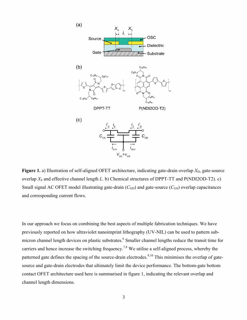
Figure 2. a) FIB-SEM micrograph showing cross-section through device with NIL patterned gate and
photo-patterned dielectric. b) – e) Cross-polarised micrographs of inkjet printed DPPT-TT and
P(NDI2OD-T2) on top of devices with PL patterned gate and PL patterned dielectric, with polarisers
oriented at 0° and 90°.
Figure 2 shows micrographs of the fabricated devices. The self-aligned architecture was verified using
focussed ion-beam scanning electron microscopy (FIB-SEM) (Helios Nanolab, FEI) whereby a cross-
section through the substrate is milled by irradiation with gallium ions. Note in order to achieve this
sputtered gold and platinum are deposited onto the region of interest pre-milling, and these layers are
also visible in the micrograph. Sub-micron NIL patterned channel lengths of L = 730 nm and PL
patterned channel lengths of L = 3.8 µm were measured. Optical microscopy was used to determine
channel widths of W = 5.4 ± 0.01 µm for PL and W = 5.0 ± 0.01 µm for NIL patterned gates (full details
shown in table SI in the Supplementary Material). Self-aligned overlaps of less than XOL ≤ 210 ± 10 nm
were measured across all substrates.
6
Cross-polarised microscopy of inkjet printed semiconductors revealed no evidence of birefringence,
suggesting a predominantly amorphous layer of DPPT-TT. This is consistent with previous reports,17
where significant crystallinity was observed after annealing at 320°C – much higher than our 150°C we
use to avoid irreversible deformation of our plastic substrate. Interestingly we did observe evidence of
birefringence (and hence possibly preferential crystallinity) in P(NDI2OD-T2) which was correlated
with print direction. During printing the inkjet nozzle rastered from left-right, top-bottom, as looking at
the optical micrographs in figure 2. This is consistent with previous reports of the influence of long
range order on charge transport,19 and semicrystalline face-on π-stacking in P(NDI2OD-T2).20,21
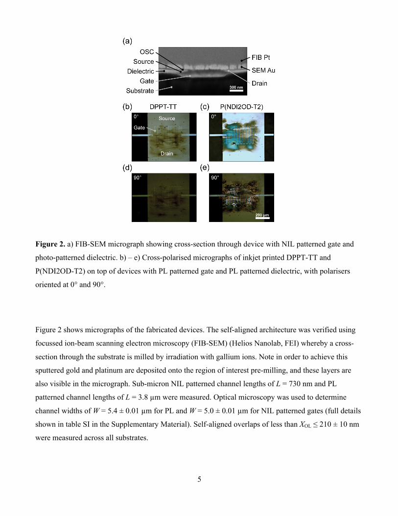
OFETs were biased in the transdiode regime (VDS = VGS) and a frequency modulated voltage vGS(f)
superimposed on the DC gate bias.6 By observing the decoupled AC component of the current in turn at
both source and drain electrodes (i’S, i’D), we measured the admittance of the OFET in response to an
AC signal, as shown in figure 3. For this we used a network analyser (Agilent 5061B) and a high
bandwidth transimpedance amplifier (Femto DHCPA-100) with a gain of 2×10³ V A-1 (see figure S2 in
the Supporting Material for a schematic of this setup). The transconductance region was fitted between
0.5 kHz < f < 7.3 kHz; the capacitance limited region was fitted between 3.5 MHz < f < 6.6 MHz (details
of these regions are discussed below). Deviations at f < 500 Hz and f > 7 MHz are artefacts of the
measurement setup.
Figure 3. Admittance measurements of a P(NDI2OD-T2) OFET with NIL patterned gate, and gravure
printed dielectric for a range of operating biases 10 V ≤ |VGS| ≤ 30 V, where the device is biased in the

7
transdiode regime (VGS = VDS). Admittance is measured at the a) drain and b) source electrodes. Red
circles (●) indicate the extracted cutoff frequencies, fD and fS respectively.
Figure 3 shows an example of the admittance measurements performed to determine the limit of
switching behaviour in our OFETs. In order to interpret these plots we consider first how the gate-drain
(XD) and gate-source (XS) overlaps effectively form parallel plate capacitors across the gate dielectric
layer. This overlap capacitance is proportional to the length of the overlap, COL ∝ XOL. Figure 1c)
illustrates the impact of these capacitors on the small signal AC behaviour of the OFET. From this figure
we note that the effective drain and source currents (i’D, i’S respectively) comprise both the channel and
capacitive current contributions. It can be shown that these additional current pathways yield two
operating regimes in the OFET, as described by equation 1 (shown for the drain electrode case).1,6
�D′=�D−�G,D (1a) =� M�GS−�2�� �GD�GS (1b) =�M�GSinthelimitofsmall� �2�� �GD�GSinthelimitoflarge� (1c)
For low frequency modulation of the gate bias the effective drain current i’D is dictated by the channel
transconductance gM. However at high frequencies the capacitive current contribution through the gate
dielectric increases, ultimately dominating the output. In this regime the gate modulation of the channel
transconductance is dwarfed by parasitic capacitive current flow and the transistor no longer acts as a
current amplifier for the input signal.

8
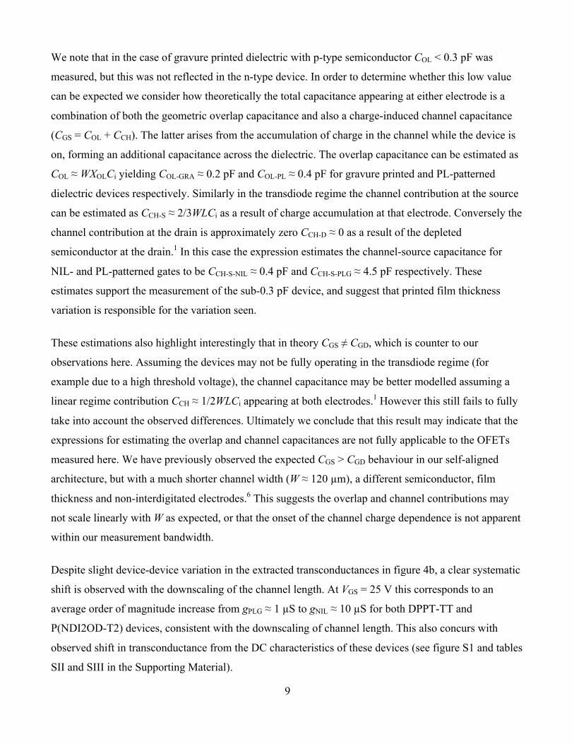
Figure 4. Summary of AC admittance measurements. Extracted a) capacitances, b) transconductances.
c) Calculated cut-off frequencies. d) Calculated transition frequencies.
Figure 4 summarises the measurements of different architecture and semiconductor variants. Devices
show exceptionally low overlap capacitances in the range COL < 1.2 pF. This equates to channel-width
normalised overlap capacitances in the range (0.15 ± 0.01) pF mm-1 < C*OL < (0.23 ± 0.01) pF mm-1,
consistent with previous reports for self-aligned inkjet printed architectures.22 This is achieved
irrespective of having an order-of-magnitude larger interdigitated channel width (W ≈ 5000 µm
compared to W = 500 µm in previous report), demonstrating the benefits of our processing approach.
9
We note that in the case of gravure printed dielectric with p-type semiconductor COL < 0.3 pF was
measured, but this was not reflected in the n-type device. In order to determine whether this low value
can be expected we consider how theoretically the total capacitance appearing at either electrode is a
combination of both the geometric overlap capacitance and also a charge-induced channel capacitance
(CGS = COL + CCH). The latter arises from the accumulation of charge in the channel while the device is
on, forming an additional capacitance across the dielectric. The overlap capacitance can be estimated as
COL ≈ WXOLCi yielding COL-GRA ≈ 0.2 pF and COL-PL ≈ 0.4 pF for gravure printed and PL-patterned
dielectric devices respectively. Similarly in the transdiode regime the channel contribution at the source
can be estimated as CCH-S ≈ 2/3WLCi as a result of charge accumulation at that electrode. Conversely the
channel contribution at the drain is approximately zero CCH-D ≈ 0 as a result of the depleted
semiconductor at the drain.1 In this case the expression estimates the channel-source capacitance for
NIL- and PL-patterned gates to be CCH-S-NIL ≈ 0.4 pF and CCH-S-PLG ≈ 4.5 pF respectively. These
estimates support the measurement of the sub-0.3 pF device, and suggest that printed film thickness
variation is responsible for the variation seen.
These estimations also highlight interestingly that in theory CGS ≠ CGD, which is counter to our
observations here. Assuming the devices may not be fully operating in the transdiode regime (for
example due to a high threshold voltage), the channel capacitance may be better modelled assuming a
linear regime contribution CCH ≈ 1/2WLCi appearing at both electrodes.1 However this still fails to fully
take into account the observed differences. Ultimately we conclude that this result may indicate that the
expressions for estimating the overlap and channel capacitances are not fully applicable to the OFETs
measured here. We have previously observed the expected CGS > CGD behaviour in our self-aligned
architecture, but with a much shorter channel width (W ≈ 120 µm), a different semiconductor, film
thickness and non-interdigitated electrodes.6 This suggests the overlap and channel contributions may
not scale linearly with W as expected, or that the onset of the channel charge dependence is not apparent
within our measurement bandwidth.
Despite slight device-device variation in the extracted transconductances in figure 4b, a clear systematic
shift is observed with the downscaling of the channel length. At VGS = 25 V this corresponds to an
average order of magnitude increase from gPLG ≈ 1 µS to gNIL ≈ 10 µS for both DPPT-TT and
P(NDI2OD-T2) devices, consistent with the downscaling of channel length. This also concurs with
observed shift in transconductance from the DC characteristics of these devices (see figure S1 and tables
SII and SIII in the Supporting Material).
10
We also observed that the gate-drain and gate-source capacitances are voltage independent. The voltage-
dependency observed in the NIL gate, gravure printed dielectric devices in figure 4a) cannot be deemed
as significant, as it becomes increasingly difficult to fit the capacitive regime in devices approaching
10 MHz (as limited by the coaxial probing used in the measurement setup).
The combination of the measurements in figure 4a) and 4b) yields the drain and source cutoff
frequencies shown in figure 4c). Equations 2 and 3 show the expressions used, where fD, fS, gD and gS
are the drain and source cutoff frequencies, and drain and source transconductances, respectively.
�D=�D2� �GD (2) �S=�S2� �GS (3)
For high cutoff frequencies a combination of both high transconductance and low capacitance is desired.
Peak performance was measured in devices with NIL-patterned gate, gravure printed dielectric and
DPPT-TT and P(NDI2OD-T2) semiconductors, with fD = 5.5 ± 0.2 MHz, and fS = 9.0 ± 0.3 MHz at VGS
= 30 V respectively (we note that the DPPT-TT device failed under bias during the 30 V drain
measurement, hence 25 V is the highest recorded drain value).
While drain and source cutoff frequencies are useful indicators of device performance, the transition
frequency (equation 4) is a more complete and conservative figure of merit for assessing device
performance, taking into account both CGD and CGS and giving a better indicator of the actual
performance achievable in a circuit application.
�T=�2�( �GD+�GS) (4)
Figure 4d) shows the calculated transition frequencies with a peak value of fT = 3.3 ± 0.2 MHz at VGS =
30 V measured for NIL-patterned gate, gravure printed dielectric and P(NDI2OD-T2) semiconductor. A
summary of these results is shown in Table I. For transition frequency estimates an average of gD and gS
is used to minimise any uncertainty in the two drain and source measurements. A comparison between
the directly extracted transconductance compared to estimates derived from DC measurements is shown
in table SIII in the Supporting Material. We note that using the value of gm derived from the transfer
characteristics in general underestimates fT. We attribute this to the relatively low stability of the un-
encapsulated devices, which were stored for a period of one day between DC and AC testing, as well as

11
the additional uncertainty introduced by using two independent setups measurements to determine fT
instead of one.
TABLE I. Summary of drain cutoff-, source cutoff- and transition frequencies for architecture variants. Extracted at VGS = 30 V unless otherwise indicated.
Gate Dielectric OSC fD (MHz) fS (MHz) fT (MHz) PL PL p 0.5 ± 0.1 0.6 ± 0.1 0.3 ± 0.1 PL PL n 0.4 ± 0.1 0.5 ± 0.1 0.2 ± 0.1
NIL PL p 5.6 ± 0.2 2.9 ± 0.1 2.2 ± 0.1 NIL PL n 0.9 ± 0.1 1.2 ± 0.1 0.5 ± 0.1 NIL GRA p 4.6 ± 0.2a 9.0 ± 0.3 2.8 ± 0.2a NIL GRA n 5.5 ± 0.2 8.0 ± 0.2 3.3 ± 0.2
aVGS = 25 V
We have shown the benefits of combining multiple fabrication technologies to yield multi-megahertz
switching OFETs, as well as the importance of considering the AC frequency response of devices. The
switching speed of our devices exceeds many state-of-the-art reports for OFETs on plastic.25,26 Self-
alignment yielded very low geometric overlap between gate-drain and gate-source electrodes, as
confirmed via FIB-SEM. This was verified by admittance measurements, revealing sub-pF capacitances.
These gave exceptionally low channel-width normalised overlap capacitances, despite the fabrication
challenge of fabricating large W/L ratio devices. Gravure printing (versus photo-patterning) the
dielectric yields thinner layers at expense of some device-device variation, yielding an order of
magnitude reduction in the overlap capacitance. Deviations from the predicted capacitances at both
electrodes suggest that further refinement of the model of overlap and channel capacitance contributions
is required for these devices.
Finally we note that measured capacitances were invariant with channel length, an indicator of reliable
self-aligned processing, and that nanoimprint lithography patterned sub-micron gates yielded an order of
magnitude boost in the observed channel transconductance, directly resulting in higher frequency cutoffs
for these devices. Even when considering the more conservative transition frequency, megahertz
operating frequencies are obtained.
S. G. Higgins was supported by the Engineering and Physical Sciences Research Council (EPSRC)
under grant number EP/P505550/1. Parts of this work have also been supported by the European

12
Commission’s 7th Framework Programme (FP7/2007-2013) under grant agreement no 247978
(POLARIC).
See supplemental material at [URL will be inserted by AIP] for details of device DC characterisation
data, and a schematic of the AC measurement setup.
1 M. Caironi, Y.-Y. Noh, and H. Sirringhaus, Semicond. Sci. Technol. 26, 034006 (2011).
2 M. Cirit, IEEE Trans. Comput. Des. Integr. Circuits Syst. 8, 1033 (1989).
3 V. Subramanian, in Org. Field-Effect Transistors (2007), pp. 489–505.
4 K. Myny, M. Rockelé, A. Chasin, S. Member, D. Pham, J. Steiger, S. Botnaras, D. Weber, B. Herold, J. Ficker, B. Van Der Putten, G.H. Gelinck, J. Genoe, W. Dehaene, and P. Heremans, IEEE Trans. Electron Devices 61, 2387 (2014).
5 R. Blache and J. Krumm, Circuits Conf. 208 (2009).
6 S.G. Higgins, B.V.O. Muir, J. Wade, J. Chen, B. Striedinger, H. Gold, B. Stadlober, M. Caironi, J.-S. Kim, J.H.G. Steinke, and A.J. Campbell, Adv. Electron. Mater. 1, 1500024 (2015).
7 V. Wagner, P. Wö bkenberg, A. Hoppe, and J. Seekamp, Appl. Phys. Lett. 89, 243515 (2006).
8 S.M. Sze and K.K. Ng., in Phys. Semicond. Devices, edited by S.M. Sze and K.K. Ng., 3rd ed. (John Wiley & Sons, Inc, Hoboken, NJ, USA, 2007), pp. 293–373.
9 U. Palfinger, C. Auner, H. Gold, A. Haase, J. Kraxner, T. Haber, M. Sezen, W. Grogger, G. Domann, G. Jakopic, J.R. Krenn, and B. Stadlober, Adv. Mater. 22, 5115 (2010).
10 H. Gold, A. Haase, A. Fian, C. Prietl, B. Striedinger, F. Zanella, N. Marjanović, R. Ferrini, J. Ring, K.-D. Lee, R. Jiawook, A. Drost, M. König, R. Müller, K. Myny, J. Genoe, U. Kleb, H. Hirshy, R. Prétôt, J. Kraxner, R. Schmied, and B. Stadlober, Org. Electron. 22, 140 (2015).
11 H. Klauk, Organic Electronics II: More Materials and Applications (Wiley-VCH Verlag & Co., Weinheim, 2012).
12 S.G. Higgins, F.L. Boughey, R. Hills, J.H.G. Steinke, B.V.O. Muir, and A.J. Campbell, ACS Appl. Mater. Interfaces 7, 5045 (2015).
13 M.M. Voigt, A. Guite, D.-Y. Chung, R.U.A. Khan, A.J. Campbell, D.D.C. Bradley, F. Meng, J.H.G. Steinke, S. Tierney, I. McCulloch, H. Penxten, L. Lutsen, O. Douheret, J. Manca, U. Brokmann, K. Sönnichsen, D. Hülsenberg, W. Bock, C. Barron, N. Blanckaert, S. Springer, J. Grupp, and A. Mosley, Adv. Funct. Mater. 20, 239 (2010).

13
14 M. Kastler and S. Köhler, WO 2010/136385 A1 (2010).
15 N.L. Vaklev, R. Müller, B.V.O. Muir, D.T. James, R. Pretot, P. van der Schaaf, J. Genoe, J.-S. Kim, J.H.G. Steinke, and A.J. Campbell, Adv. Mater. Interfaces 1, 1300123 (2014).
16 S. Mandal, G. Dell’Erba, A. Luzio, S.G. Bucella, A. Perinot, A. Calloni, G. Berti, G. Bussetti, L. Duò, A. Facchetti, Y.-Y. Noh, and M. Caironi, Org. Electron. 20, 132 (2015).
17 Z. Chen, M.J. Lee, R. Shahid Ashraf, Y. Gu, S. Albert-Seifried, M. Meedom Nielsen, B. Schroeder, T.D. Anthopoulos, M. Heeney, I. McCulloch, and H. Sirringhaus, Adv. Mater. 24, 647 (2012).
18 H. Yan, Z. Chen, Y. Zheng, C. Newman, J.R. Quinn, F. Dötz, M. Kastler, and A. Facchetti, Nature 457, 679 (2009).
19 A. Luzio, L. Criante, V. D’Innocenzo, and M. Caironi, Sci. Rep. 3, 3425 (2013).
20 H. Sirringhaus, Adv. Mater. 26, 1319 (2014).
21 J. Rivnay, M. Toney, Y. Zheng, I. Kauvar, Z. Chen, V. Wagner, A. Facchetti, and A. Salleo, Adv. Mater. 22, 4359 (2010).
22 Y.-Y. Noh, N. Zhao, M. Caironi, and H. Sirringhaus, Nat. Nanotechnol. 2, 784 (2007).
23 J. Haddock, X. Zhang, S. Zheng, Q. Zhang, S. Marder, and B. Kippelen, Org. Electron. 7, 45 (2006).
24 F. Ante, D. Kälblein, T. Zaki, U. Zschieschang, K. Takimiya, M. Ikeda, T. Sekitani, T. Someya, J.N. Burghartz, K. Kern, and H. Klauk, Small 8, 73 (2012).
25 S. Mandal and Y.-Y. Noh, Semicond. Sci. Technol. 30, 064003 (2015).
26 V. Subramanian, J. Cen, A. de la Fuente Vornbrock, G. Grau, H. Kang, R. Kitsomboonloha, D. Soltman, and H.-Y. Tseng, Proc. IEEE 103, 567 (2015).


![[Chapter III] Basic Knowledge of Discrete Semiconductor ......transistors (IGBTs) Power transistors (2SAxx,2SBxx,2SCxx,2SDxx, TTAxx,TTBxx,TTCxx,TTDxx) Types of Transistors Transistors](https://static.fdocuments.net/doc/165x107/5e766014341a1a707d5f4c34/chapter-iii-basic-knowledge-of-discrete-semiconductor-transistors-igbts.jpg)