
Selecting and Testing 32kHz Crystal Oscillators - Doc8333
24
AVR4100: Selecting and testing 32kHz crystal oscillators for Atmel AVR microcontrollers Features • Crystal oscillator basics • PCB design considerations • Testing crystal robustness • Test firmware included • Crystal recommendation guide 1 Introduction This application note summarizes the crystal basics, PCB layout considerations, and how to test a crystal in your application. A crystal selection guide shows recommended crystals tested by experts and found suitable for various oscillator modules in different Atmel ® AVR ® families. Test firmware and test reports from various crystal vendors are included. 8-bit Atmel Microcontrollers Application Note Rev. 8333D-AVR-07/11
-
Upload
mahnoor-malik -
Category
Documents
-
view
112 -
download
6
Transcript of Selecting and Testing 32kHz Crystal Oscillators - Doc8333

AVR4100: Selecting and testing 32kHz crystal oscillators for Atmel AVR microcontrollers
Features • Crystal oscillator basics • PCB design considerations • Testing crystal robustness • Test firmware included • Crystal recommendation guide
1 Introduction This application note summarizes the crystal basics, PCB layout considerations, and how to test a crystal in your application. A crystal selection guide shows recommended crystals tested by experts and found suitable for various oscillator modules in different Atmel®AVR® families. Test firmware and test reports from various crystal vendors are included.
8-bit Atmel Microcontrollers Application Note
Rev. 8333D-AVR-07/11
2 AVR4100 8333D-AVR-07/11
2 Crystal oscillator basics
Many readers are familiar with the basic crystal oscillator theory, and are only interested in how to test their applications. These readers may skip chapters 2 and 3, and start reading chapter 4.
2.1 Introduction A crystal oscillator uses the mechanical resonance of a vibrating piezoelectric material to generate a very stable clock signal. The frequency is usually used to provide a stable clock signal or to keep track of time; hence, crystal oscillators are widely used in RF and digital circuits.
Crystals are available from various vendors in a variety of shapes and sizes, and can vary widely in performance and specifications. Understanding the parameters and the oscillator circuit are essential for a robust application stable over variations in temperature, humidity, power supply, and process.
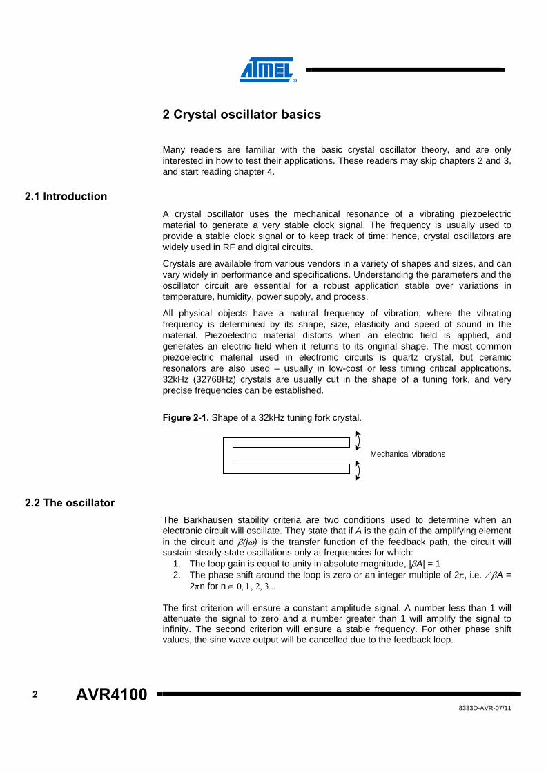
All physical objects have a natural frequency of vibration, where the vibrating frequency is determined by its shape, size, elasticity and speed of sound in the material. Piezoelectric material distorts when an electric field is applied, and generates an electric field when it returns to its original shape. The most common piezoelectric material used in electronic circuits is quartz crystal, but ceramic resonators are also used – usually in low-cost or less timing critical applications. 32kHz (32768Hz) crystals are usually cut in the shape of a tuning fork, and very precise frequencies can be established.
Figure 2-1. Shape of a 32kHz tuning fork crystal.
2.2 The oscillator The Barkhausen stability criteria are two conditions used to determine when an electronic circuit will oscillate. They state that if A is the gain of the amplifying element in the circuit and β(jω) is the transfer function of the feedback path, the circuit will sustain steady-state oscillations only at frequencies for which:
1. The loop gain is equal to unity in absolute magnitude, |βA| = 1 2. The phase shift around the loop is zero or an integer multiple of 2π, i.e. ∠βA =
2πn for n ∈ 0, 1, 2, 3... The first criterion will ensure a constant amplitude signal. A number less than 1 will attenuate the signal to zero and a number greater than 1 will amplify the signal to infinity. The second criterion will ensure a stable frequency. For other phase shift values, the sine wave output will be cancelled due to the feedback loop.
Mechanical vibrations
AVR4100
38333D-AVR-07/11
Figure 2-2. Feedback loop.
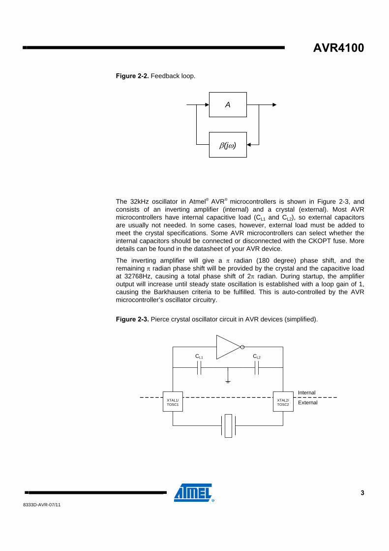
The 32kHz oscillator in Atmel® AVR® microcontrollers is shown in Figure 2-3, and consists of an inverting amplifier (internal) and a crystal (external). Most AVR microcontrollers have internal capacitive load (CL1 and CL2), so external capacitors are usually not needed. In some cases, however, external load must be added to meet the crystal specifications. Some AVR microcontrollers can select whether the internal capacitors should be connected or disconnected with the CKOPT fuse. More details can be found in the datasheet of your AVR device.
The inverting amplifier will give a π radian (180 degree) phase shift, and the remaining π radian phase shift will be provided by the crystal and the capacitive load at 32768Hz, causing a total phase shift of 2π radian. During startup, the amplifier output will increase until steady state oscillation is established with a loop gain of 1, causing the Barkhausen criteria to be fulfilled. This is auto-controlled by the AVR microcontroller’s oscillator circuitry.
Figure 2-3. Pierce crystal oscillator circuit in AVR devices (simplified).
A
β(jω)
XTAL1/TOSC1
XTAL2/TOSC2
Internal
External
CL1 CL2

4 AVR4100 8333D-AVR-07/11
2.3 Electrical model The equivalent electric circuit of a crystal is shown in Figure 2-4. The series RLC network is called the motional arm, and gives an electrical description of the mechanical behavior of the crystal, where C1 represents the elasticity of the quartz, L1 represents the vibrating mass, and R1 represents losses due to damping. C0 is called the shunt or static capacitance, and is the sum of the electrical parasitic capacitance due to the crystal housing and electrodes. If a capacitance meter is used to measure the crystal capacitance, only C0 will be measured (C1 will have no effect).
Figure 2-4. Crystal oscillator equivalent circuit.
By using the Laplace transform, two resonant frequencies can be found in this network. The series resonant frequency, fs, depends only on C1 and L1, and the parallel or anti-resonant frequency, fp, also includes C0. The reactance vs. frequency characteristics can be found in Figure 2-5.
Equation 2-1. Series resonant frequency.
Equation 2-2. Parallel resonant frequency.
C1 L1 R1
C0
1121
CLfs π
=
0
1
11
12
1CC
CLf p +=
π

AVR4100
58333D-AVR-07/11
Figure 2-5. Crystal reactance characteristics.
Crystals below 30MHz can be operated at any frequency between the series and parallel resonant frequencies, which means that they are inductive in operation. High-frequency crystals above 30MHz are usually operated at the series resonant frequency or overtone frequencies, which occur at multiples of the fundamental frequency. Adding a capacitive load, CL, to the crystal will cause a shift in frequency given by Equation 2-3. The crystal frequency can be tuned by varying the load capacitance, and this is called frequency pulling.
Equation 2-3. Parallel resonant frequency.
Inductive
Capacitive
Frequency
Series resonant freq
Parallell resonant freq
⎟⎟⎠
⎞⎜⎜⎝
⎛+
=Δ)(2 0
1
Ls CC
Cff

6 AVR4100 8333D-AVR-07/11
2.4 Equivalent series resistance (ESR) The equivalent series resistance (ESR) is an electrical representation of the mechanical losses, and at the series resonant frequency, fs, it is equal to R1 in the electrical model. The ESR is a very important parameter, and can be found in the crystal datasheet. The ESR will usually be dependent of the crystal’s physical size, and small crystals (especially small SMD crystals) typically have higher losses and ESR values than larger crystals.
Higher ESR values will load the inverting amplifier more, and too high an ESR may cause unstable oscillator operation. Unity gain will not be achieved, and the Barkhausen criterion will not be fulfilled.
2.5 Q-factor and stability The frequency stability of a crystal is given by the Q-factor. The Q-factor is the ratio between the energy stored in the crystal and the sum of all energy losses. Typically, quartz crystals have Q in the range of 10,000 to 100,000, compared to perhaps 100 for a LC oscillator. Ceramic resonators have lower Q than quartz crystals, and are more sensitive to capacitive load (pull ability is higher).
Equation 2-4. Q-factor.
Several factors can affect the frequency stability: Mechanical stress induced by mounting, shock or vibration stress, variations in power supply, load impedance, temperature, magnetic and electric fields, and crystal aging may all have an effect. Crystal vendors usually list such parameters in their datasheets.
2.6 Start-up time During startup, noise will be amplified in the inverting amplifier. The crystal will act as a band pass filter, and feed back only the crystal resonance frequency component, which will be amplified. Before steady state oscillation is achieved, the loop gain of the crystal/inverting amplifier loop is greater than 1, and the signal amplitude will increase. At steady state, the loop gain will fulfill the Barkhausen criteria with a loop gain of 1 and constant amplitude.
Factors affecting the startup time:
• High-ESR crystal will start more slowly than low-ESR crystals
• High Q-factor crystals will start more slowly than low Q-factor crystals
• High load capacitance will increase startup time
• Oscillator amplifier drive capabilities (see more details on oscillator allowance in Section 4.2)
In addition, crystal frequency will affect the startup time (faster crystals will start faster), but this parameter is fixed for 32kHz crystals
∑=
LOSS
STORED
EEQ

AVR4100
78333D-AVR-07/11
Figure 2-6. Startup signal of a crystal oscillator.
2.7 Temperature tolerance Typical tuning fork crystals are usually cut to center the nominal frequency at 25°C. Above and below 25°C, the frequency will decrease with a parabolic characteristic, as shown in Figure 2-7. The frequency shift is given by Equation 2-5, where f0 is the target frequency at T0 (typically 32768Hz at 25°C) and the PPM is the temperature tolerance coefficient given by the crystal datasheet.
Equation 2-5. Effect of temperature variation.
Figure 2-7. Typical temperature vs. frequency characteristics of a crystal.
-1
0
1
1 69 137 205 273 341 409 477 545 613 681 749 817 885 953 1021 1089 1157 1225 1293 1361
200 ))(1( TTPPMff −−=
Temperature 25°C
Freq
uenc
y

8 AVR4100 8333D-AVR-07/11
3 PCB layout and design considerations
Even the best performing oscillator circuits and high-quality crystals will not perform well if the layout and materials used during assembly are not carefully considered. Ultra low power 32kHz oscillators typically dissipate significantly below 1μW, and the current flowing in the circuit is, therefore, extremely small. In addition, the crystal frequency is highly dependent on the capacitive load.
To increase the robustness of the oscillator, we recommend these guidelines during PCB layout:
• Signal lines from XTAL1/TOSC1 and XTAL2/TOSC2 to the crystal should be as short as possible to reduce parasitic capacitance and increase noise and crosstalk immunity. Any kind of sockets should be avoided.
• Shield the crystal and signal lines by surrounding it with a ground plane and guard ring.
• Avoid routing digital lines, especially clock lines, close to the crystal lines. For multi-layer PCB boards, avoid routing signals below the crystal lines.
• PCB cleaning is recommended to reduce flux residues from soldering.
• Use high-quality PCB and soldering materials.
• Dust and humidity will increase parasitic capacitance and reduce signal isolation, so protective coating is recommended.
AVR4100
98333D-AVR-07/11
4 Testing crystal oscillation robustness
4.1 Introduction The 32kHz crystal oscillator driver of AVR microcontrollers is optimized for very low power consumption, and thus the crystal driver strength is limited. Overloading the crystal driver may cause the oscillator to not start, or it may be affected (stopped temporarily) e.g. due to a noise spike or increased capacitive load caused by contamination or proximity of a hand.
This means that care should be taken when selecting and testing the crystal to ensure proper robustness in your application. The two important crystal parameters are equivalent series resistance (ESR) and load capacitance (CL).
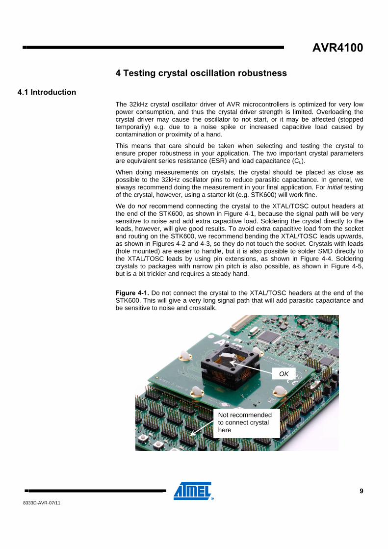
When doing measurements on crystals, the crystal should be placed as close as possible to the 32kHz oscillator pins to reduce parasitic capacitance. In general, we always recommend doing the measurement in your final application. For initial testing of the crystal, however, using a starter kit (e.g. STK600) will work fine.
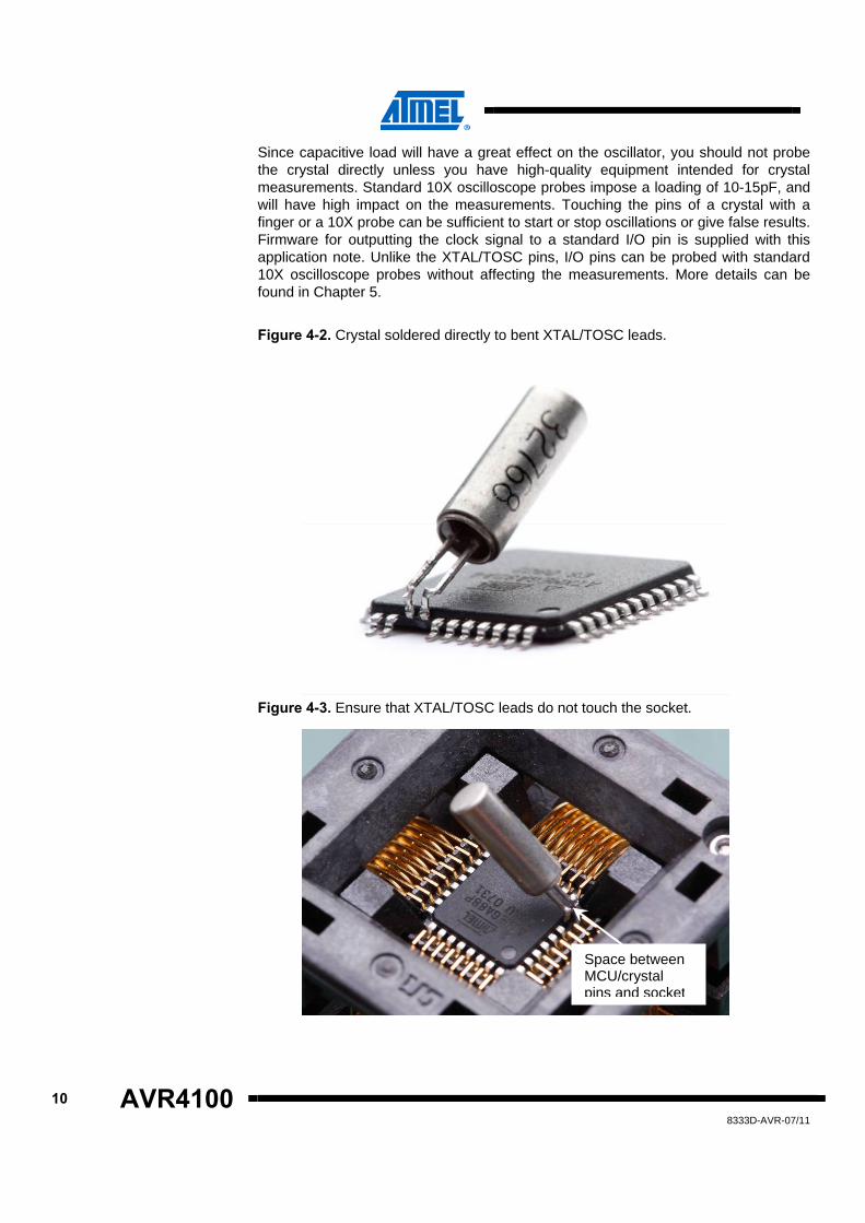
We do not recommend connecting the crystal to the XTAL/TOSC output headers at the end of the STK600, as shown in Figure 4-1, because the signal path will be very sensitive to noise and add extra capacitive load. Soldering the crystal directly to the leads, however, will give good results. To avoid extra capacitive load from the socket and routing on the STK600, we recommend bending the XTAL/TOSC leads upwards, as shown in Figures 4-2 and 4-3, so they do not touch the socket. Crystals with leads (hole mounted) are easier to handle, but it is also possible to solder SMD directly to the XTAL/TOSC leads by using pin extensions, as shown in Figure 4-4. Soldering crystals to packages with narrow pin pitch is also possible, as shown in Figure 4-5, but is a bit trickier and requires a steady hand.
Figure 4-1. Do not connect the crystal to the XTAL/TOSC headers at the end of the STK600. This will give a very long signal path that will add parasitic capacitance and be sensitive to noise and crosstalk.
OK
Not recommended to connect crystal here
10 AVR4100 8333D-AVR-07/11
Since capacitive load will have a great effect on the oscillator, you should not probe the crystal directly unless you have high-quality equipment intended for crystal measurements. Standard 10X oscilloscope probes impose a loading of 10-15pF, and will have high impact on the measurements. Touching the pins of a crystal with a finger or a 10X probe can be sufficient to start or stop oscillations or give false results. Firmware for outputting the clock signal to a standard I/O pin is supplied with this application note. Unlike the XTAL/TOSC pins, I/O pins can be probed with standard 10X oscilloscope probes without affecting the measurements. More details can be found in Chapter 5.
Figure 4-2. Crystal soldered directly to bent XTAL/TOSC leads.
Figure 4-3. Ensure that XTAL/TOSC leads do not touch the socket.
Space between MCU/crystal pins and socket
AVR4100
118333D-AVR-07/11
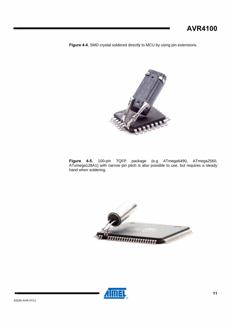
Figure 4-4. SMD crystal soldered directly to MCU by using pin extensions.
Figure 4-5. 100-pin TQFP package (e.g ATmega6490, ATmega2560, ATxmega128A1) with narrow pin pitch is also possible to use, but requires a steady hand when soldering.

12 AVR4100 8333D-AVR-07/11
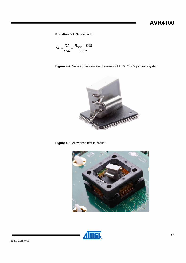
4.2 Negative resistance test and safety factor The negative resistance test finds the margin between the crystal amplifier load used in your application and the maximum load. At the maximum load, the amplifier will choke and the oscillations will stop. This point is called the oscillator allowance (OA). The oscillator allowance can be found by temporarily adding a variable series resistor between the amplifier output (XTAL2/TOSC2) lead and the crystal, as shown in Figure 4-6. The series resistor should be increased until the crystal stops oscillating. The oscillator allowance will then be the sum of this series resistance, RMAX, and the ESR. We recommend using a potentiometer with a range of at least ESR < RPOT < 5 ESR.
Finding a correct RMAX value can be a bit tricky because no exact oscillator allowance point exists. Before the oscillator stops, you may observe a gradual frequency reduction, and there may also be a start-stop hysteresis. After the oscillator stops, you will need to reduce the RMAX value by 10-50kΩ before oscillations resume. We recommend performing a power cycling each time after the variable resistor is increased. RMAX will then be the resistor value where the oscillator does not start after a power cycling. Note that the startup times will be quite long at the oscillator allowance point, so please be patient.
Equation 4-1. Oscillator allowance.
Figure 4-6. Measuring oscillator allowance/RMAX
We recommend using a high quality potentiometer with low parasitic capacitance (an SMD potentiometer suitable for RF will usually give the best results). However, if you are able to achieve good oscillator allowance/RMAX with a cheap potentiometer, you will be safe.
When the maximum series resistance is found, you can find the safety factor from Equation 4-2. Various MCU and crystal vendors operate with different safety factor recommendations. The safety factor is intended to add margin for negative effects of different variables such as oscillator amplifier gain, change due to power supply and temperature variations, process variations, and load capacitance. The 32kHz oscillator amplifier on AVR microcontrollers is temperature and power compensated, and so by having these variables more or less constant, we can reduce the requirements for the safety factor compared to other MCU/IC manufacturers. The safety factor recommendations can be found in Table 4-1.
ESRROA MAX +=
ESR R
XTAL1/TOSC1 XTAL2/TOSC2
AVR4100
138333D-AVR-07/11
Equation 4-2. Safety factor.
Figure 4-7. Series potentiometer between XTAL2/TOSC2 pin and crystal.
Figure 4-8. Allowance test in socket.
ESRESRR
ESROASF MAX +
==
14 AVR4100 8333D-AVR-07/11
Table 4-1. Safety factor recommendations. Safety factor Recommendation
5< Excellent
4 Very good
3 Good
<3 Not recommended
AVR4100
158333D-AVR-07/11
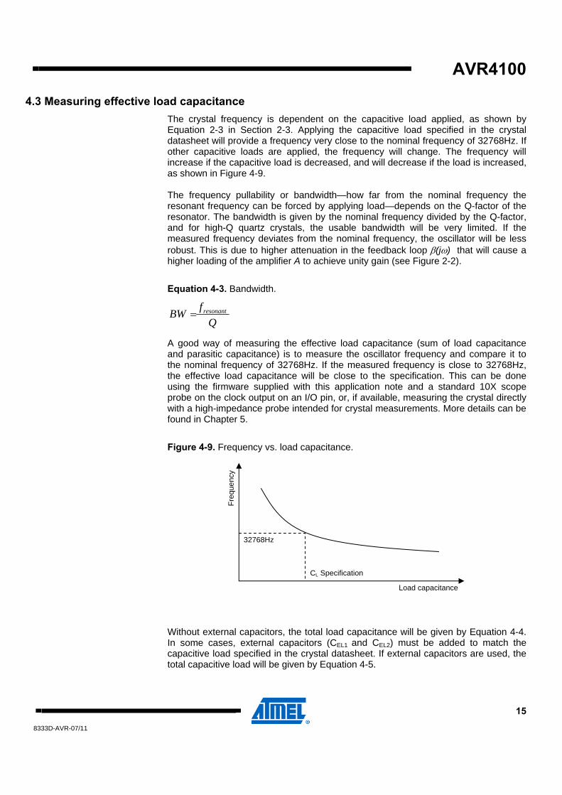
4.3 Measuring effective load capacitance The crystal frequency is dependent on the capacitive load applied, as shown by Equation 2-3 in Section 2-3. Applying the capacitive load specified in the crystal datasheet will provide a frequency very close to the nominal frequency of 32768Hz. If other capacitive loads are applied, the frequency will change. The frequency will increase if the capacitive load is decreased, and will decrease if the load is increased, as shown in Figure 4-9. The frequency pullability or bandwidth—how far from the nominal frequency the resonant frequency can be forced by applying load—depends on the Q-factor of the resonator. The bandwidth is given by the nominal frequency divided by the Q-factor, and for high-Q quartz crystals, the usable bandwidth will be very limited. If the measured frequency deviates from the nominal frequency, the oscillator will be less robust. This is due to higher attenuation in the feedback loop β(jω) that will cause a higher loading of the amplifier A to achieve unity gain (see Figure 2-2).
Equation 4-3. Bandwidth.
A good way of measuring the effective load capacitance (sum of load capacitance and parasitic capacitance) is to measure the oscillator frequency and compare it to the nominal frequency of 32768Hz. If the measured frequency is close to 32768Hz, the effective load capacitance will be close to the specification. This can be done using the firmware supplied with this application note and a standard 10X scope probe on the clock output on an I/O pin, or, if available, measuring the crystal directly with a high-impedance probe intended for crystal measurements. More details can be found in Chapter 5.
Figure 4-9. Frequency vs. load capacitance. Without external capacitors, the total load capacitance will be given by Equation 4-4. In some cases, external capacitors (CEL1 and CEL2) must be added to match the capacitive load specified in the crystal datasheet. If external capacitors are used, the total capacitive load will be given by Equation 4-5.
Freq
uenc
y
Load capacitance
32768Hz
CL Specification
QfBW resonant=

16 AVR4100 8333D-AVR-07/11
Equation 4-4. Total capacitive load without external capacitors.
Equation 4-5. Total capacitive load with external capacitors.
Figure 4-10. Crystal circuit with internal, parasitic and external capacitors.
2121
2211 ))((PPLL
PLPLL CCCC
CCCCC+++++
=∑
XTAL1/TOSC1
XTAL2/TOSC2
Internal
External
CL1 CL2
CEL1 CEL2CP1 CP2
212121
222111 ))((
ELELPPLL
ELPLELPLL CCCCCC
CCCCCCC+++++++++
=∑
AVR4100
178333D-AVR-07/11
5 Test firmware
Test firmware for outputting the clock signal to an I/O port that may be loaded with a standard 10X probe is included in the .zip file distributed with this application note. The crystal electrodes should not be measured directly if you do not have very high impedance probes intended for such measurements.
• Compile the source code (set the device define if required), and program the .hex file into the device.
• Apply Vcc within the operating range listed in the datasheet, connect the crystal between XTAL1/TOSC1 and XTAL2/TOSC2, and measure the clock signal on the output pin.
• The output compare pin will differ from device to device, so you need to look in the code to find which I/O pin will output the clock signal.
5.1 TinyAVR The clock signal is output to PORTB by using an endless while loop that toggles the port, and hence the clock signal will be divided by 10 (nominal frequency of 3276.8Hz). All Atmel® tinyAVR® devices are supported. To use a 32768Hz crystal as the clock source for the device, the low-frequency crystal oscillator must be selected by setting CKSEL fuses. Look in the datasheet for details.
5.2 MegaAVR An asynchronous timer overflow is used to toggle an I/O pin, and hence the clock signal will be divided by 2 (nominal frequency of 16384Hz). All megaAVR® devices are supported, but a device family define needs to be set (see list of defines in the .c file).
5.3 XMEGA The Atmel® AVR®XMEGA® families have support for outputting the peripheral clock directly to an I/O port. No clock division will be done. The firmware will set up the external low-frequency crystal as the system clock and enable low-power mode. The clock signal will be output on port PD7.
5.4 UC3 UC3 support will be included in a future release of this application note.
18 AVR4100 8333D-AVR-07/11
6 Crystal recommendations Table 6-2 is a selection of crystals that have been tested and found suitable for various AVR microcontrollers. Using crystal-MCU combinations from the table below will ensure good compatibility, and is highly recommended for users with little or limited crystal expertise. Even though the crystal-MCU combinations are tested by highly experienced crystal oscillator experts at the various crystal vendors, we still recommend testing your design as described in Chapter 4 to ensure that no issues have been introduced during layout, soldering, etc.
Please refer to the .zip file attached to this application note for test reports and crystal datasheets.
Table 6-1 shows a list of the different oscillator modules, and a list of devices where these modules are included can be found in Chapter 7.
Table 6-1. Overview of oscillators in AVR devices. # Oscillator module Description
1 X32K_2v7 2.7-5.5V oscillator used in MegaAVR devices
2 X32K_1v8 1.8-5.5V oscillator used in MegaAVR/TinyAVR devices
3 X32K_1v8_ULP 1.8-3.6V ultra low power oscillator used in MegaAVR/TinyAVR pico power devices
4 X32K_XMEGA 1.6-3.6V ultra low power oscillator used in XMEGA devices – oscillator setup in normal mode
5 X32K_XMEGA 1.6-3.6V ultra low power oscillator used in XMEGA devices – oscillator setup in low power mode
6 X32K_XRTC32 1.6-3.6V ultra low power RTC oscillator used in XMEGA devices with battery backup

AVR4100
198333D-AVR-07/11
Table 6-2. Recommended 32kHz crystals.
Vendor Type Mount Oscillator modules tested and approved (see table 6-1)
Frequency Tolerance
[±ppm]
Load Capacitance [pF]
Equivalent Series
Resistance (ESR) [kΩ]
Microcrystal CC7V-T1A SMD 1, 2, 3, 4, 5 20 / 100(1) 7.0 / 9.0 / 12.5 50 / 70
Abracon ABS06 SMD 2 20 12.5 90
Cardinal CPFB SMD 2, 3, 4, 5 20 12.5 50
Cardinal CTF6 HOLE 2, 3, 4, 5 20 12.5 50
Cardinal CTF8 HOLE 2, 3, 4, 5 20 12.5 50
Endrich Citizen CFS206 HOLE 1, 2, 3, 4 20 12.5 35
Endrich Citizen CM315 SMD 1, 2, 3, 4 20 12.5 70
Epson Tyocom MC-306 SMD 1, 2, 3 20 / 50 12.5(2) 50
Fox FSXLF SMD 2, 3, 4, 5 20 12.5 65
Fox FX135 SMD 2, 3, 4, 5 20 12.5 70
Fox FX122 SMD 2, 3, 5 20 12.5 90
Fox FSRLF SMD 1, 2, 3, 4, 5 20 12.5 50
NDK NX3215SA SMD 1, 2 ,3 20 12.5 80
Seiko SSP-T7-FL SMD 3 20 6 65
Seiko SSP-T7-F SMD 1, 2 20 12.5 65
Seiko SSP-T7-F SMD 4 20 7 65
Seiko SSP-T7-FL SMD 5 20 4.4 65
Notes:
1) Tighter and wider frequency tolerances on request
2) 12.5pF standard, but 6pF to ∞ available on request
The table will be kept updated with more crystal vendors and recommendations for oscillator modules included in XMEGA and UC3 devices.
Are you representing a crystal vendor and not on the list? Please contact [email protected] to participate in our crystal recommendation program.

20 AVR4100 8333D-AVR-07/11
7 Oscillator module overview
Table 7-1 shows a list of which 32kHz oscillators are included in various Atmel® MegaAVR®, Atmel® tinyAVR® and Atmel® XMEGA® devices. The list will be extended with UC3 devices in future releases.
Table 7-1. Oscillator module overview.
Device Family Device Oscillator module
MegaAVR ATmega128 X32K_2v7 MegaAVR ATmega1280 X32K_1v8 MegaAVR ATmega1281 X32K_1v8 MegaAVR ATmega1284P X32K_1v8_ULP MegaAVR ATmega128A X32K_2v7 MegaAVR ATmega16 X32K_2v7 MegaAVR ATmega162 X32K_1v8 MegaAVR ATmega164A X32K_1v8_ULP MegaAVR ATmega164P X32K_1v8_ULP MegaAVR ATmega164PA X32K_1v8_ULP MegaAVR ATmega165A X32K_1v8_ULP MegaAVR ATmega165P X32K_1v8_ULP MegaAVR ATmega165PA X32K_1v8_ULP MegaAVR ATmega168 X32K_1v8 MegaAVR ATmega168A X32K_1v8_ULP MegaAVR ATmega168P X32K_1v8_ULP MegaAVR ATmega168PA X32K_1v8_ULP MegaAVR ATmega169 X32K_1v8 MegaAVR ATmega169A X32K_1v8_ULP MegaAVR ATmega169P X32K_1v8_ULP MegaAVR ATmega169PA X32K_1v8_ULP MegaAVR ATmega16A X32K_2v7 MegaAVR ATmega2560 X32K_1v8 MegaAVR ATmega2561 X32K_1v8 MegaAVR ATmega32 X32K_2v7 MegaAVR ATmega324A X32K_1v8_ULP MegaAVR ATmega324P X32K_1v8_ULP MegaAVR ATmega324PA X32K_1v8_ULP MegaAVR ATmega3250A X32K_1v8_ULP MegaAVR ATmega3250P X32K_1v8_ULP MegaAVR ATmega3250PA X32K_1v8_ULP

AVR4100
218333D-AVR-07/11
Device Family Device Oscillator module
MegaAVR ATmega325A X32K_1v8_ULP MegaAVR ATmega32A X32K_2v7 MegaAVR ATmega48 X32K_1v8 MegaAVR ATmega48A X32K_1v8_ULP MegaAVR ATmega325P X32K_1v8_ULP MegaAVR ATmega325PA X32K_1v8_ULP MegaAVR ATmega328 X32K_1v8 MegaAVR ATmega328P X32K_1v8_ULP MegaAVR ATmega328PA X32K_1v8_ULP MegaAVR ATmega329 X32K_1v8 MegaAVR ATmega3290A X32K_1v8_ULP MegaAVR ATmega3290P X32K_1v8_ULP MegaAVR ATmega3290PA X32K_1v8_ULP MegaAVR ATmega329A X32K_1v8_ULP MegaAVR ATmega329P X32K_1v8_ULP MegaAVR ATmega329PA X32K_1v8_ULP MegaAVR ATmega32A X32K_2v7 MegaAVR ATmega48 X32K_1v8 MegaAVR ATmega48A X32K_1v8_ULP MegaAVR ATmega48P X32K_1v8_ULP MegaAVR ATmega48PA X32K_1v8_ULP MegaAVR ATmega64 X32K_2v7 MegaAVR ATmega640 X32K_1v8 MegaAVR ATmega644A X32K_1v8_ULP MegaAVR ATmega644P X32K_1v8_ULP MegaAVR ATmega644PA X32K_1v8_ULP MegaAVR ATmega6450A X32K_1v8_ULP MegaAVR ATmega6450P X32K_1v8_ULP MegaAVR ATmega645A X32K_1v8_ULP MegaAVR ATmega645P X32K_1v8_ULP MegaAVR ATmega649 X32K_1v8 MegaAVR ATmega6490 X32K_1v8_ULP MegaAVR ATmega6490A X32K_1v8_ULP MegaAVR ATmega6490P X32K_1v8_ULP MegaAVR ATmega649A X32K_1v8_ULP MegaAVR ATmega649P X32K_1v8_ULP TinyAVR ATtiny84A X32K_1v8 TinyAVR ATtiny85 X32K_1v8 TinyAVR ATtiny861 X32K_1v8

22 AVR4100 8333D-AVR-07/11
Device Family Device Oscillator module
MegaAVR ATmega48P X32K_1v8_ULP MegaAVR ATmega48PA X32K_1v8_ULP MegaAVR ATmega64 X32K_2v7 MegaAVR ATmega640 X32K_1v8 MegaAVR ATmega644A X32K_1v8_ULP MegaAVR ATmega644P X32K_1v8_ULP MegaAVR ATmega644PA X32K_1v8_ULP MegaAVR ATmega6450A X32K_1v8_ULP MegaAVR ATmega6450P X32K_1v8_ULP MegaAVR ATmega645A X32K_1v8_ULP MegaAVR ATmega645P X32K_1v8_ULP MegaAVR ATmega649 X32K_1v8 MegaAVR ATmega6490 X32K_1v8_ULP MegaAVR ATmega6490A X32K_1v8_ULP MegaAVR ATmega6490P X32K_1v8_ULP MegaAVR ATmega649A X32K_1v8_ULP MegaAVR ATmega649P X32K_1v8_ULP MegaAVR ATmega64A X32K_2v7 MegaAVR ATmega8 X32K_2v7 MegaAVR ATmega88 X32K_1v8 MegaAVR ATmega88A X32K_1v8_ULP MegaAVR ATmega88P X32K_1v8_ULP MegaAVR ATmega88PA X32K_1v8_ULP MegaAVR ATmega8A X32K_2v7 TinyAVR ATtiny2313A X32K_1v8 TinyAVR ATtiny24 X32K_1v8 TinyAVR ATtiny24A X32K_1v8 TinyAVR ATtiny25 X32K_1v8 TinyAVR ATtiny261 X32K_1v8 TinyAVR ATtiny261A X32K_1v8 TinyAVR ATtiny4313 X32K_1v8 TinyAVR ATtiny44 X32K_1v8 TinyAVR ATtiny44A X32K_1v8 TinyAVR ATtiny45 X32K_1v8 TinyAVR ATtiny461 X32K_1v8 TinyAVR ATtiny461A X32K_1v8 TinyAVR ATtiny84 X32K_1v8 TinyAVR ATtiny861A X32K_1v8 XMEGA ATxmega128A1 X32K_XMEGA
AVR4100
238333D-AVR-07/11
Device Family Device Oscillator module
XMEGA ATxmega128A3 X32K_XMEGA XMEGA ATxmega128A4 X32K_XMEGA XMEGA ATxmega128D3 X32K_XMEGA XMEGA ATxmega128D4 X32K_XMEGA XMEGA ATxmega16A4 X32K_XMEGA XMEGA ATxmega16D4 X32K_XMEGA XMEGA ATxmega192A1 X32K_XMEGA XMEGA ATxmega192A3 X32K_XMEGA XMEGA ATxmega192D3 X32K_XMEGA XMEGA ATxmega256A1 X32K_XMEGA XMEGA ATxmega256D3 X32K_XMEGA XMEGA ATxmega32A4 X32K_XMEGA XMEGA ATxmega32D4 X32K_XMEGA XMEGA ATxmega348A1 X32K_XMEGA XMEGA ATxmega64A1 X32K_XMEGA XMEGA ATxmega64A3 X32K_XMEGA XMEGA ATxmega64A4 X32K_XMEGA XMEGA ATxmega64D3 X32K_XMEGA XMEGA ATxmega64D4 X32K_XMEGA XMEGA ATxmega256A3B X32K_XRTC32
8333D-AVR-07/11
Atmel Corporation 2325 Orchard Parkway San Jose, CA 95131 USA Tel: (+1)(408) 441-0311 Fax: (+1)(408) 487-2600 www.atmel.com
Atmel Asia Limited Unit 01-5 & 16, 19F BEA Tower, Milennium City 5 418 Kwun Tong Road Kwun Tong, Kowloon HONG KONG Tel: (+852) 2245-6100 Fax: (+852) 2722-1369
Atmel Munich GmbH Business Campus Parkring 4 D-85748 Garching b. Munich GERMANY Tel: (+49) 89-31970-0 Fax: (+49) 89-3194621
Atmel Japan 9F, Tonetsu Shinkawa Bldg. 1-24-8 Shinkawa Chou-ku, Tokyo 104-0033 JAPAN Tel: (+81) 3523-3551 Fax: (+81) 3523-7581
© 2011 Atmel Corporation. All rights reserved.
Atmel®, Atmel logo and combinations thereof, AVR®, AVR® logo, tinyAVR®, XMEGA® and others, are the registered trademarks or trademarks of Atmel Corporation or its subsidiaries. Other terms and product names may be trademarks of others. Disclaimer: The information in this document is provided in connection with Atmel products. No license, express or implied, by estoppel or otherwise, to any intellectual property right is granted by this document or in connection with the sale of Atmel products. EXCEPT AS SET FORTH IN THE ATMEL TERMS AND CONDITIONS OF SALES LOCATED ON THE ATMEL WEBSITE, ATMEL ASSUMES NO LIABILITY WHATSOEVER AND DISCLAIMS ANY EXPRESS, IMPLIED OR STATUTORY WARRANTY RELATING TO ITS PRODUCTS INCLUDING, BUT NOT LIMITED TO, THE IMPLIED WARRANTY OF MERCHANTABILITY, FITNESS FOR A PARTICULAR PURPOSE, OR NON-INFRINGEMENT. IN NO EVENT SHALL ATMEL BE LIABLE FOR ANY DIRECT, INDIRECT, CONSEQUENTIAL, PUNITIVE, SPECIAL OR INCIDENTAL DAMAGES (INCLUDING, WITHOUT LIMITATION, DAMAGES FOR LOSS AND PROFITS, BUSINESS INTERRUPTION, OR LOSS OF INFORMATION) ARISING OUT OF THE USE OR INABILITY TO USE THIS DOCUMENT, EVEN IF ATMEL HAS BEEN ADVISED OF THE POSSIBILITY OF SUCH DAMAGES. Atmel makes no representations or warranties with respect to the accuracy or completeness of the contents of this document and reserves the right to make changes to specifications and product descriptions at any time without notice. Atmel does not make any commitment to update the information contained herein. Unless specifically provided otherwise, Atmel products are not suitable for, and shall not be used in, automotive applications. Atmel products are not intended, authorized, or warranted for use as components in applications intended to support or sustain life.