
SECTION 8.1 – CHARACTERIZATION OF COMPARATORS CMOS Slides/Chapter08-2UP(4_8_02).pdf · SECTION...
44
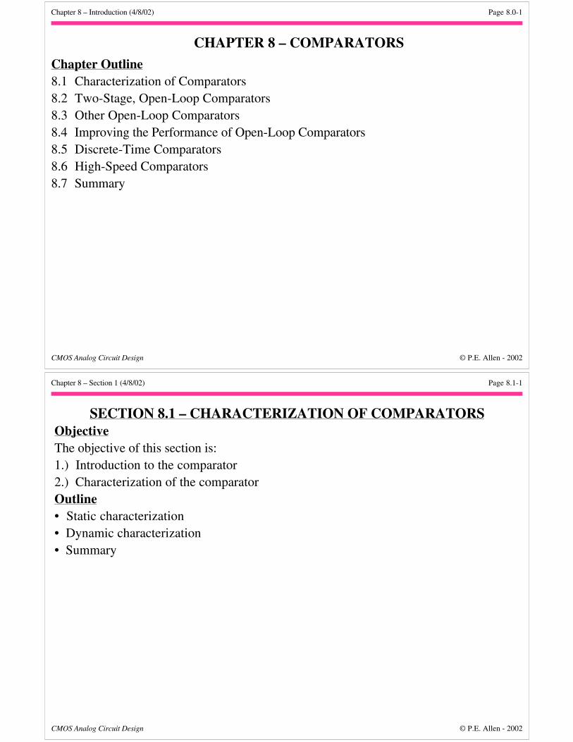
Chapter 8 – Introduction (4/8/02) Page 8.0-1 CMOS Analog Circuit Design © P.E. Allen - 2002 CHAPTER 8 – COMPARATORS Chapter Outline 8.1 Characterization of Comparators 8.2 Two-Stage, Open-Loop Comparators 8.3 Other Open-Loop Comparators 8.4 Improving the Performance of Open-Loop Comparators 8.5 Discrete-Time Comparators 8.6 High-Speed Comparators 8.7 Summary Chapter 8 – Section 1 (4/8/02) Page 8.1-1 CMOS Analog Circuit Design © P.E. Allen - 2002 SECTION 8.1 – CHARACTERIZATION OF COMPARATORS Objective The objective of this section is: 1.) Introduction to the comparator 2.) Characterization of the comparator Outline • Static characterization • Dynamic characterization • Summary
Transcript of SECTION 8.1 – CHARACTERIZATION OF COMPARATORS CMOS Slides/Chapter08-2UP(4_8_02).pdf · SECTION...
Chapter 8 – Introduction (4/8/02) Page 8.0-1
CMOS Analog Circuit Design © P.E. Allen - 2002
CHAPTER 8 – COMPARATORS
Chapter Outline8.1 Characterization of Comparators8.2 Two-Stage, Open-Loop Comparators8.3 Other Open-Loop Comparators8.4 Improving the Performance of Open-Loop Comparators8.5 Discrete-Time Comparators8.6 High-Speed Comparators8.7 Summary
Chapter 8 – Section 1 (4/8/02) Page 8.1-1
CMOS Analog Circuit Design © P.E. Allen - 2002
SECTION 8.1 – CHARACTERIZATION OF COMPARATORSObjectiveThe objective of this section is:1.) Introduction to the comparator2.) Characterization of the comparatorOutline• Static characterization• Dynamic characterization• Summary
Chapter 8 – Section 1 (4/8/02) Page 8.1-2
CMOS Analog Circuit Design © P.E. Allen - 2002
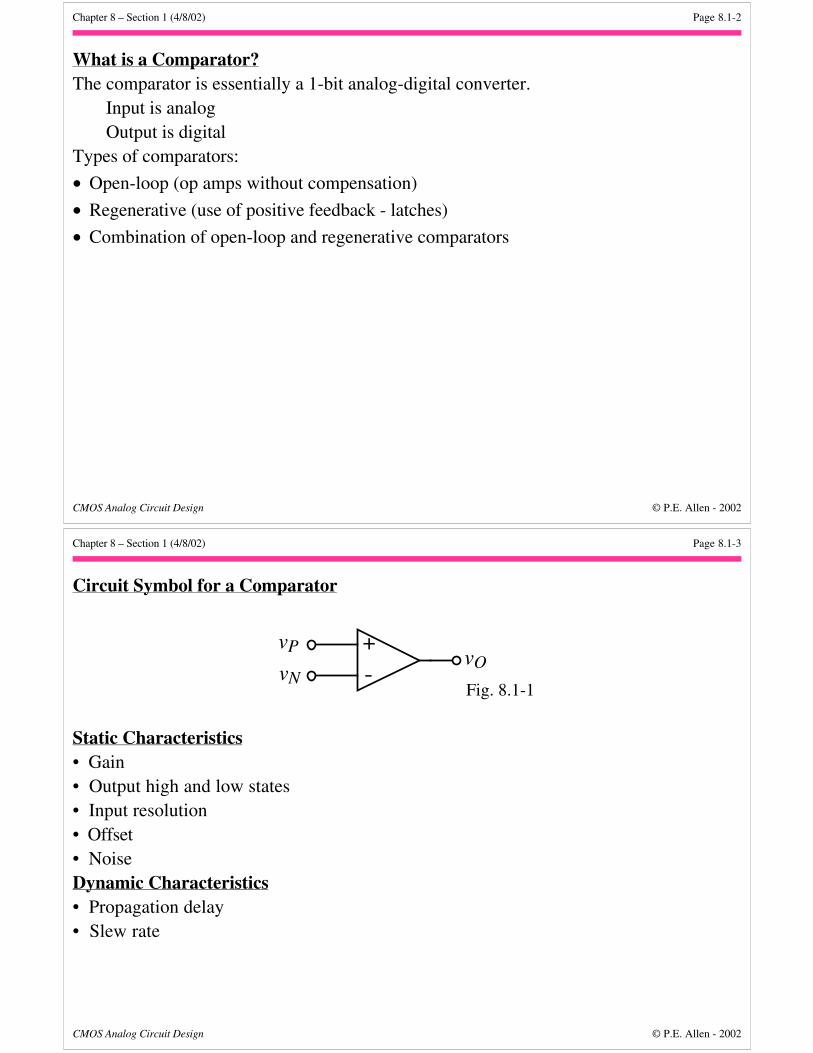
What is a Comparator?The comparator is essentially a 1-bit analog-digital converter.
Input is analogOutput is digital
Types of comparators:
• Open-loop (op amps without compensation)
• Regenerative (use of positive feedback - latches)
• Combination of open-loop and regenerative comparators
Chapter 8 – Section 1 (4/8/02) Page 8.1-3
CMOS Analog Circuit Design © P.E. Allen - 2002
Circuit Symbol for a Comparator
+-
vP
vNvO
Fig. 8.1-1
Static Characteristics• Gain• Output high and low states• Input resolution• Offset• NoiseDynamic Characteristics• Propagation delay• Slew rate
Chapter 8 – Section 1 (4/8/02) Page 8.1-4
CMOS Analog Circuit Design © P.E. Allen - 2002
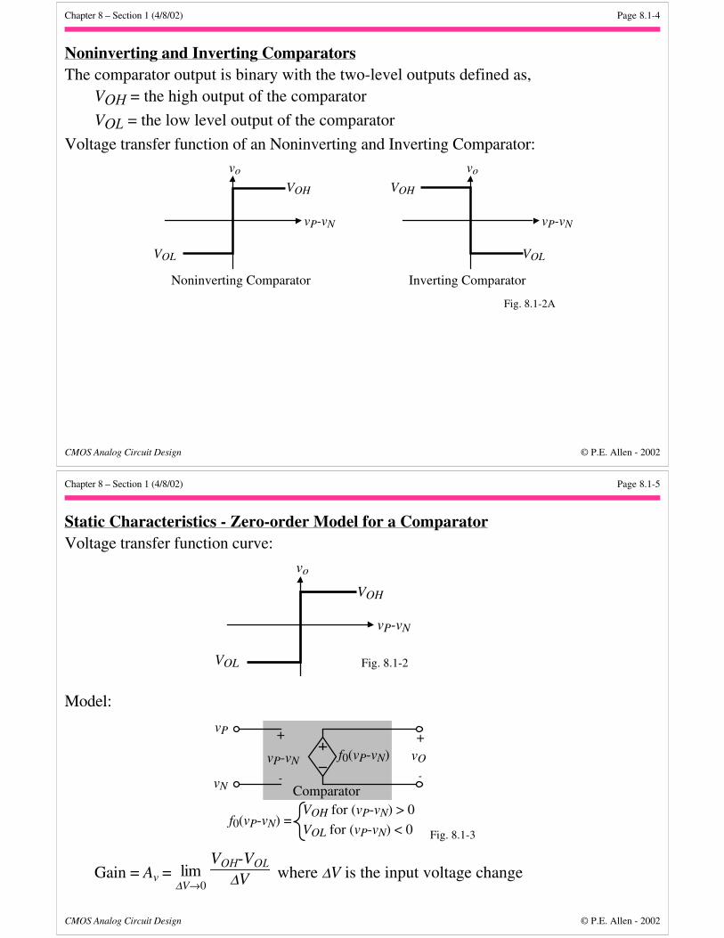
Noninverting and Inverting ComparatorsThe comparator output is binary with the two-level outputs defined as,
VOH = the high output of the comparator
VOL = the low level output of the comparator
Voltage transfer function of an Noninverting and Inverting Comparator:vo
VOH
vP-vN
VOL
Noninverting Comparator
vo
VOH
vP-vN
VOL
Inverting Comparator
Fig. 8.1-2A
Chapter 8 – Section 1 (4/8/02) Page 8.1-5
CMOS Analog Circuit Design © P.E. Allen - 2002
Static Characteristics - Zero-order Model for a ComparatorVoltage transfer function curve:
vo
VOH
vP-vN
VOL Fig. 8.1-2
Model:
f0(vP-vN)+
vO
+
- -
vP
vN
vP-vN
Comparator
f0(vP-vN) = VOH for (vP-vN) > 0
VOL for (vP-vN) < 0 Fig. 8.1-3
Gain = Av =
lim∆V→0
VOH-VOL
∆V where ∆V is the input voltage change
Chapter 8 – Section 1 (4/8/02) Page 8.1-6
CMOS Analog Circuit Design © P.E. Allen - 2002
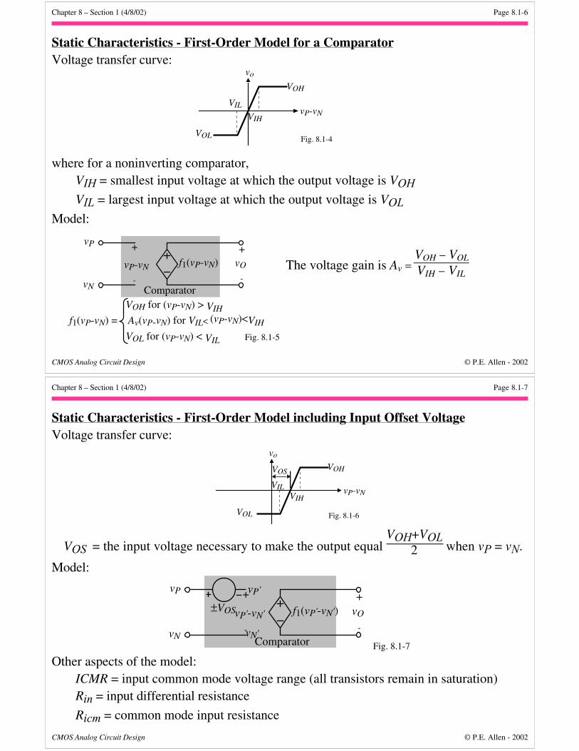
Static Characteristics - First-Order Model for a ComparatorVoltage transfer curve:
where for a noninverting comparator,VIH = smallest input voltage at which the output voltage is VOHVIL = largest input voltage at which the output voltage is VOL
Model:
The voltage gain is Av = VOH − VOL
VIH − VIL
vo
VOH
vP-vN
VOL Fig. 8.1-4
VIH
VIL
f1(vP-vN)+
vO
+
- -
vP
vN
vP-vN
Comparator
f1(vP-vN) =
VOH for (vP-vN) > VIH
VOL for (vP-vN) < VIL Fig. 8.1-5
Av(vP-vN) for VIL< (vP-vN)<VIH
Chapter 8 – Section 1 (4/8/02) Page 8.1-7
CMOS Analog Circuit Design © P.E. Allen - 2002
Static Characteristics - First-Order Model including Input Offset VoltageVoltage transfer curve:
vo
VOH
vP-vN
VOL Fig. 8.1-6
VIH
VIL
VOS
VOS = the input voltage necessary to make the output equal VOH+VOL
2 when vP = vN.
Model:
f1(vP'-vN')+
vO
+
- -
vP
vN
vP'-vN'
Comparator Fig. 8.1-7
vP'
vN'
±VOS
Other aspects of the model:ICMR = input common mode voltage range (all transistors remain in saturation)Rin = input differential resistance
Ricm = common mode input resistance
Chapter 8 – Section 1 (4/8/02) Page 8.1-8
CMOS Analog Circuit Design © P.E. Allen - 2002
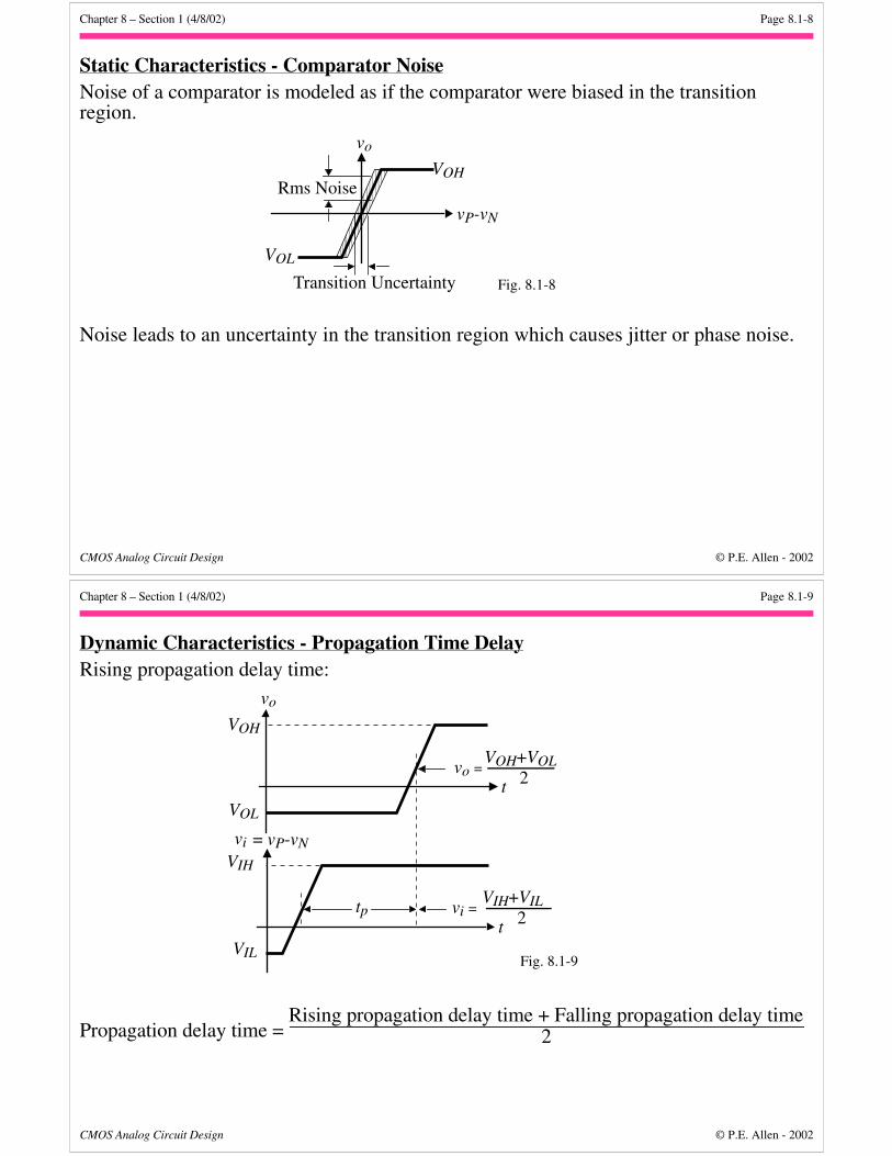
Static Characteristics - Comparator NoiseNoise of a comparator is modeled as if the comparator were biased in the transitionregion.
��vo
VOH
vP-vN
VOL
Fig. 8.1-8
Rms Noise
Transition Uncertainty
Noise leads to an uncertainty in the transition region which causes jitter or phase noise.
Chapter 8 – Section 1 (4/8/02) Page 8.1-9
CMOS Analog Circuit Design © P.E. Allen - 2002
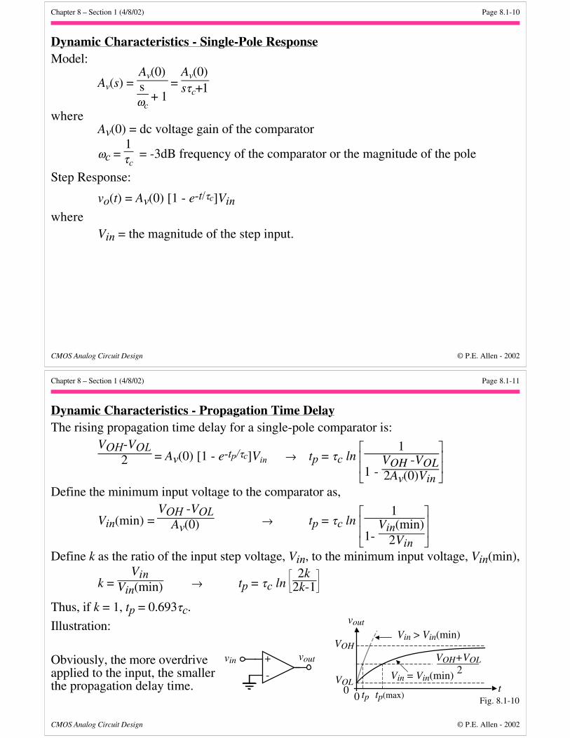
Dynamic Characteristics - Propagation Time DelayRising propagation delay time:
vo
VOH
tVOL
vi
t
Fig. 8.1-9
VIH
VIL
vo = VOH+VOL
2
vi = VIH+VIL
2tp
= vP-vN
Propagation delay time = Rising propagation delay time + Falling propagation delay time
2
Chapter 8 – Section 1 (4/8/02) Page 8.1-10
CMOS Analog Circuit Design © P.E. Allen - 2002
Dynamic Characteristics - Single-Pole ResponseModel:
Av(s) = Av(0)sωc
+ 1 =
Av(0)sτc+1
whereAv(0) = dc voltage gain of the comparator
ωc = 1τc
= -3dB frequency of the comparator or the magnitude of the pole
Step Response:
vo(t) = Av(0) [1 - e-t/τc]Vinwhere
Vin = the magnitude of the step input.
Chapter 8 – Section 1 (4/8/02) Page 8.1-11
CMOS Analog Circuit Design © P.E. Allen - 2002
Dynamic Characteristics - Propagation Time DelayThe rising propagation time delay for a single-pole comparator is:
VOH-VOL2 = Av(0) [1 - e-tp/τc]Vin → tp = τc ln
1
1 - VOH -VOL2Av(0)Vin
Define the minimum input voltage to the comparator as,
Vin(min) = VOH -VOL
Av(0) → tp = τc ln
1
1- Vin(min)
2VinDefine k as the ratio of the input step voltage, Vin, to the minimum input voltage, Vin(min),
k = Vin
Vin(min) → tp = τc ln
2k
2k-1
Thus, if k = 1, tp = 0.693τc.
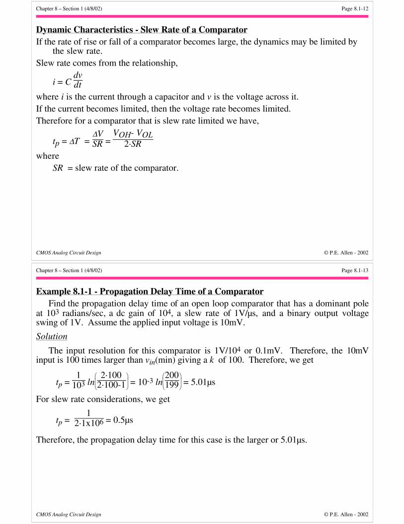
Illustration:
Obviously, the more overdriveapplied to the input, the smallerthe propagation delay time.
+
-
VOH
VOL
tp(max)0t0
VOH+VOL2
Vin > Vin(min)
Vin = Vin(min)
vin
vout
vout
Fig. 8.1-10tp
Chapter 8 – Section 1 (4/8/02) Page 8.1-12
CMOS Analog Circuit Design © P.E. Allen - 2002
Dynamic Characteristics - Slew Rate of a ComparatorIf the rate of rise or fall of a comparator becomes large, the dynamics may be limited by
the slew rate.Slew rate comes from the relationship,
i = C dvdt
where i is the current through a capacitor and v is the voltage across it.If the current becomes limited, then the voltage rate becomes limited.Therefore for a comparator that is slew rate limited we have,
tp = ∆T = ∆VSR =
VOH- VOL2·SR
whereSR = slew rate of the comparator.
Chapter 8 – Section 1 (4/8/02) Page 8.1-13
CMOS Analog Circuit Design © P.E. Allen - 2002
Example 8.1-1 - Propagation Delay Time of a ComparatorFind the propagation delay time of an open loop comparator that has a dominant pole
at 103 radians/sec, a dc gain of 104, a slew rate of 1V/µs, and a binary output voltageswing of 1V. Assume the applied input voltage is 10mV.
Solution
The input resolution for this comparator is 1V/104 or 0.1mV. Therefore, the 10mVinput is 100 times larger than vin(min) giving a k of 100. Therefore, we get
tp = 1
103 ln
2·100
2·100-1 = 10-3 ln
200
199 = 5.01µs
For slew rate considerations, we get
tp = 1
2·1x106 = 0.5µs
Therefore, the propagation delay time for this case is the larger or 5.01µs.
Chapter 8 – Section 2 (4/8/02) Page 8.2-1
CMOS Analog Circuit Design © P.E. Allen - 2002
SECTION 8.2 – TWO-STAGE OPEN-LOOP COMPARATORSObjectiveThe objective of this section is:1.) Illustrate the performance and design of a two-stage open-loop comparatorOutline• Two-stage, open-loop comparator performance• Initial states of the two-stage, open-loop comparator• Propagation delay time of a slewing, two-stage, open-loop comparator• Design of a two-stage, open-loop comparator• Summary
Chapter 8 – Section 2 (4/8/02) Page 8.2-2
CMOS Analog Circuit Design © P.E. Allen - 2002
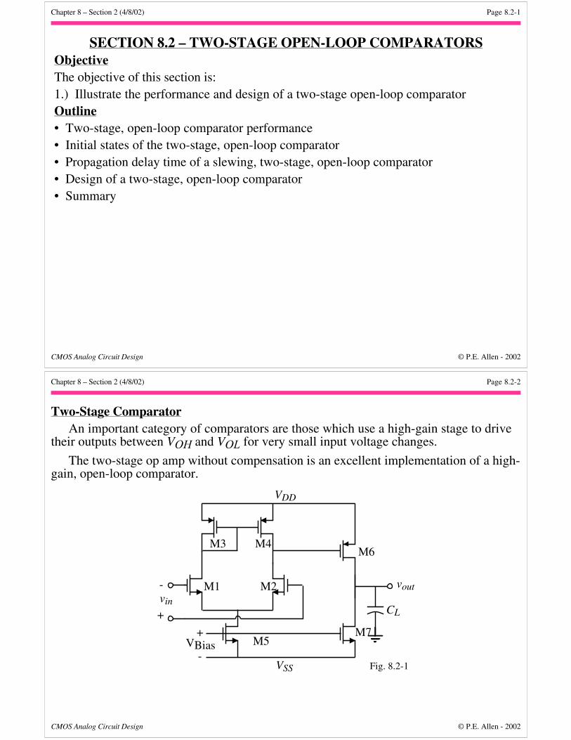
Two-Stage ComparatorAn important category of comparators are those which use a high-gain stage to drive
their outputs between VOH and VOL for very small input voltage changes.
The two-stage op amp without compensation is an excellent implementation of a high-gain, open-loop comparator.
-
+vin
M1 M2
M3 M4
M5
M6
M7
vout
VDD
VSS
VBias+
-
CL
Fig. 8.2-1
Chapter 8 – Section 2 (4/8/02) Page 8.2-3
CMOS Analog Circuit Design © P.E. Allen - 2002
Performance of the Two-Stage, Open-Loop ComparatorWe know the performance should be similar to the uncompensated two-stage op amp.Emphasis on comparator performance:• Maximum output voltage
VOH = VDD - (VDD-VG6(min)-|VTP|)
1 - 1 - 8I7
β6(VDD-VG6(min)-|VTP|)2
• Minimum output voltageVOL = VSS
• Small-signal voltage gain
Av(0) =
gm1
gds2+gds4
gm6
gds6+gds7
• PolesInput: Output:
p1 = -(gds2+gds4)
CI p2 =
-(gds6+gds7)CII
• Frequency response
Av(s) = Av(0)
s
p1 - 1
s
p2 - 1
Chapter 8 – Section 2 (4/8/02) Page 8.2-4
CMOS Analog Circuit Design © P.E. Allen - 2002
Example 8.2-1 - Performance of a Two-Stage ComparatorEvaluate VOH, VOL, Av(0), Vin(min), p1, p2, for the two-stage comparator in Fig. 8.2-1.
Assume that this comparator is the circuit of Ex. 6.3-1 with no compensation capacitor,Cc, and the minimum value of VG6 = 0V. Also, assume that CI = 0.2pF and CII = 5pF. Solution
Using the above relations, we find that
VOH = 2.5 - (2.5-0-0.7)
1 - 1 - 8·234x10-6
50x10-6·38(2.5-0-0.7)2 = 2.2V
The value of VOL is -2.5V. The gain was evaluated in Ex. 6.3-1 as Av(0) = 7696.Therefore, the input resolution is
Vin(min) = VOH-VOL
Av(0) = 4.7V7696 = 0.611mV
Next, we find the poles of the comparator, p1 and p2. From Ex. 6.3-1 we find that
p1 = - gds2 + gds4
CI = -
15x10-6(0.04+0.05)0.2x10-12 = -6.75x10⁶ (1.074MHz)
and
p2 = - gds6 + gds7
CII = -
95x10-6(0.04+0.05)5x10-12 = -1.71x10⁶ (0.272MHz)
Chapter 8 – Section 2 (4/8/02) Page 8.2-5
CMOS Analog Circuit Design © P.E. Allen - 2002
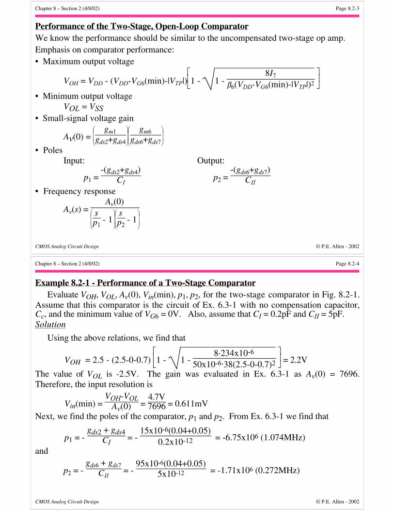
Linear Step Response of the Two-Stage ComparatorThe step response of a circuit with two real poles (p1 ≠ p2) is,
vout(t) = Av(0)Vin
1 + p2etp1
p1-p2 -
p1etp2
p1-p2
Normalizing gives,
vout’(tn ) = vout(t)
Av(0)Vin = 1 -
mm-1e-tn +
1m-1e-mtn where m =
p2p1 ≠ 1 and tn = -tp1
If p1 = p2 (m =1), then vout’(tn) = 1 - etp1 + tp1etp1 = 1 - e-tn - tne-tn
0
0.2
0.4
0.6
0.8
1
0 2 4 6 8 10Normalized Time (tn = -tp1 )
Nor
mal
ized
Out
put V
olta
ge
m = 0.25m = 0.5m = 1m = 2
m = 4
m = p2p1
Fig. 8.2-2
Chapter 8 – Section 2 (4/8/02) Page 8.2-6
CMOS Analog Circuit Design © P.E. Allen - 2002
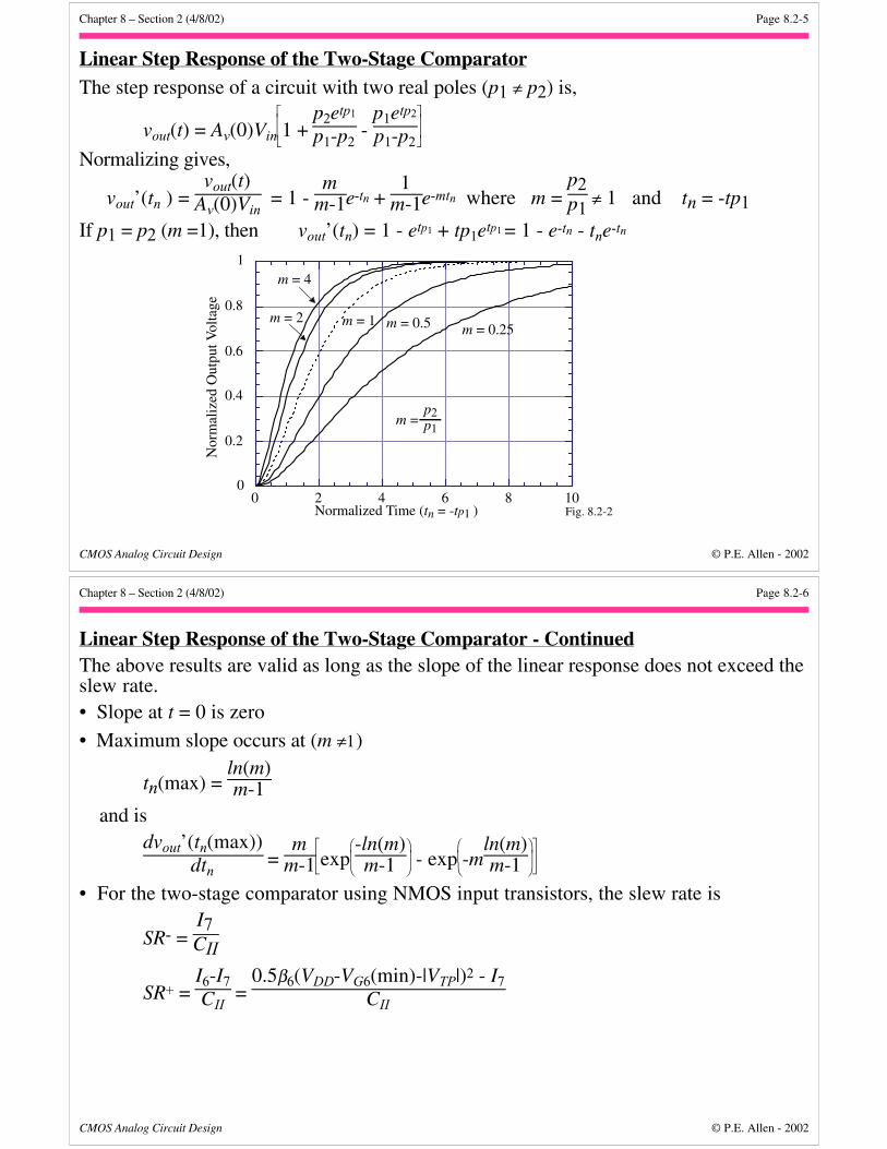
Linear Step Response of the Two-Stage Comparator - ContinuedThe above results are valid as long as the slope of the linear response does not exceed theslew rate.• Slope at t = 0 is zero
• Maximum slope occurs at (m ≠1)
tn(max) = ln(m)m-1
and isdvout’(tn(max))
dtn =
mm-1
exp
-ln(m)
m-1 - exp
-mln(m)m-1
• For the two-stage comparator using NMOS input transistors, the slew rate is
SR- = I7CII
SR+ = I6-I7CII
= 0.5β6(VDD-VG6(min)-|VTP|)2 - I7
CII
Chapter 8 – Section 2 (4/8/02) Page 8.2-7
CMOS Analog Circuit Design © P.E. Allen - 2002
Example 8.2-2 - Step Response of Ex. 8.2-1Find the maximum slope of Ex. 8.2-1 and the time at which it occurs if the magnitude
of the input step is vin(min). If the dc bias current in M7 is 100µA, at what value of loadcapacitance, CL would the transient response become slew limited? If the magnitude ofthe input step is 100vin(min), what is the new value of CL at which slewing would occur?Solution
The poles of the comparator were given in Ex. 8.2-1 as p1 = -6.75x10⁶ rads/sec. andp2 = -1.71x10⁶ rads/sec. This gives a value of m = 0.253. From the previous expressions,the maximum slope occurs at tn(max) = 1.84 secs. Dividing by |p1| gives t(max) =0.272µs. The slope of the transient response at this time is found as
dvout’(tn(max))dtn = -0.338[exp(-1.84) - exp(-0.253·1.84)] = 0.159 V/sec
Multiplying the above by |p1| givesdvout’(t(max))
dt = 1.072V/µsTherefore, if the slew rate is less than 1.072V/µs, the transient response will experienceslewing. Also, if CL ≥ 100µA/1.072V/µs or 93.3pF, the comparator will slew.
If the input is 100vin(min), then we must unnormalize the output slope as follows.dvout’(t( max))
dt = vin
vin(min) dvout’(t( max))
dt = 100·1.072V/µs = 107.2V/µs
Therefore, the comparator will now slew with a load capacitance of 0.933pF.
Chapter 8 – Section 2 (4/8/02) Page 8.2-8
CMOS Analog Circuit Design © P.E. Allen - 2002
Propagation Delay Time (Non-Slew)To find tp, we want to set 0.5(VOH-VOL) equal to vout(tn). However, vout(tn) given as
vout(tn) = Av(0)Vin
1 - m
m-1e-tn + 1
m-1e-mtn
can’t be easily solved so approximate the step response as a power series to get
vout(tn) ≈ Av(0)Vin
1 - m
m-1
1-tn+ tn2
2 + ··· + 1
m-1
1-mtn+ m2tn2
2 +··· ≈ mtn
2Av(0)Vin2
Therefore, set vout(tn) = 0.5(VOH-VOL)
VOH+VOL2 ≈
mtpn2Av(0)Vin
2or
tpn ≈ VOH+VOLmAv(0)Vin
= Vin(min)
mVin =
1mk
This approximation is particularly good for large values of k.
Chapter 8 – Section 2 (4/8/02) Page 8.2-9
CMOS Analog Circuit Design © P.E. Allen - 2002
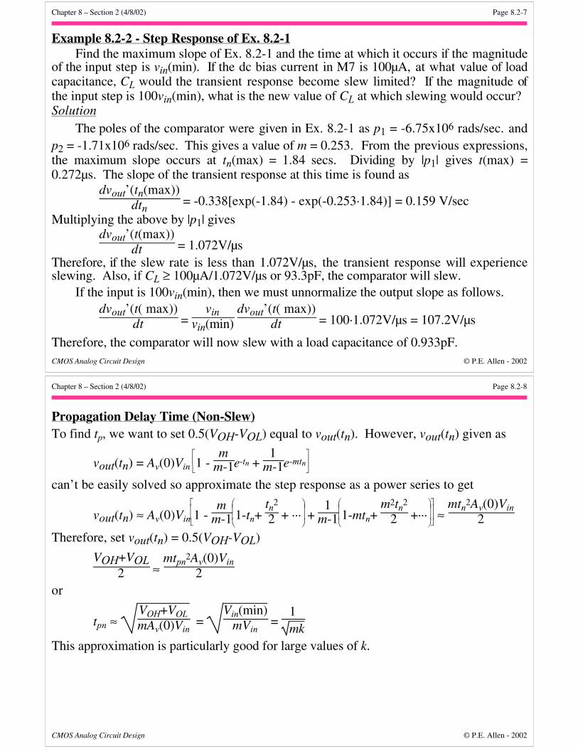
Example 8.2-3 - Propagation Delay Time of a Two-Pole Comparator (Non-Slew)Find the propagation time delay of Ex. 8.2-1 if Vin = 10mV, 100mV and 1V.
SolutionFrom Ex. 8.2-1 we know
that Vin(min) = 0.611mV and m= 0.253. For Vin = 10mV, k =16.366 which gives tpn ≈ 0.491.The propagation time delay isequal to 0.491/6.75x106 or72.9nS. This corresponds wellwith Fig. 8.2-2 where thenormalized propagation timedelay is the time at which theamplitude is 1/2k or 0.031which corresponds to tpn ofapproximately 0.5. Similarly,for Vin = 100mV and 1V we geta propagation time delay of23ns and 7.3ns, respectively.
0
0.2
0.4
0.6
0.8
1
0 2 4 6 8 10Normalized Time (tn = tp1 = t/τ1)
Nor
mal
ized
Out
put V
olta
ge
m = 0.25m = 0.5m = 1m = 2
m = 4
m = p2p1
Fig. 8.2-2A
= 0.031
0.52
12k
tp = 6.75x1060.52 = 77ns
Chapter 8 – Section 2 (4/8/02) Page 8.2-10
CMOS Analog Circuit Design © P.E. Allen - 2002
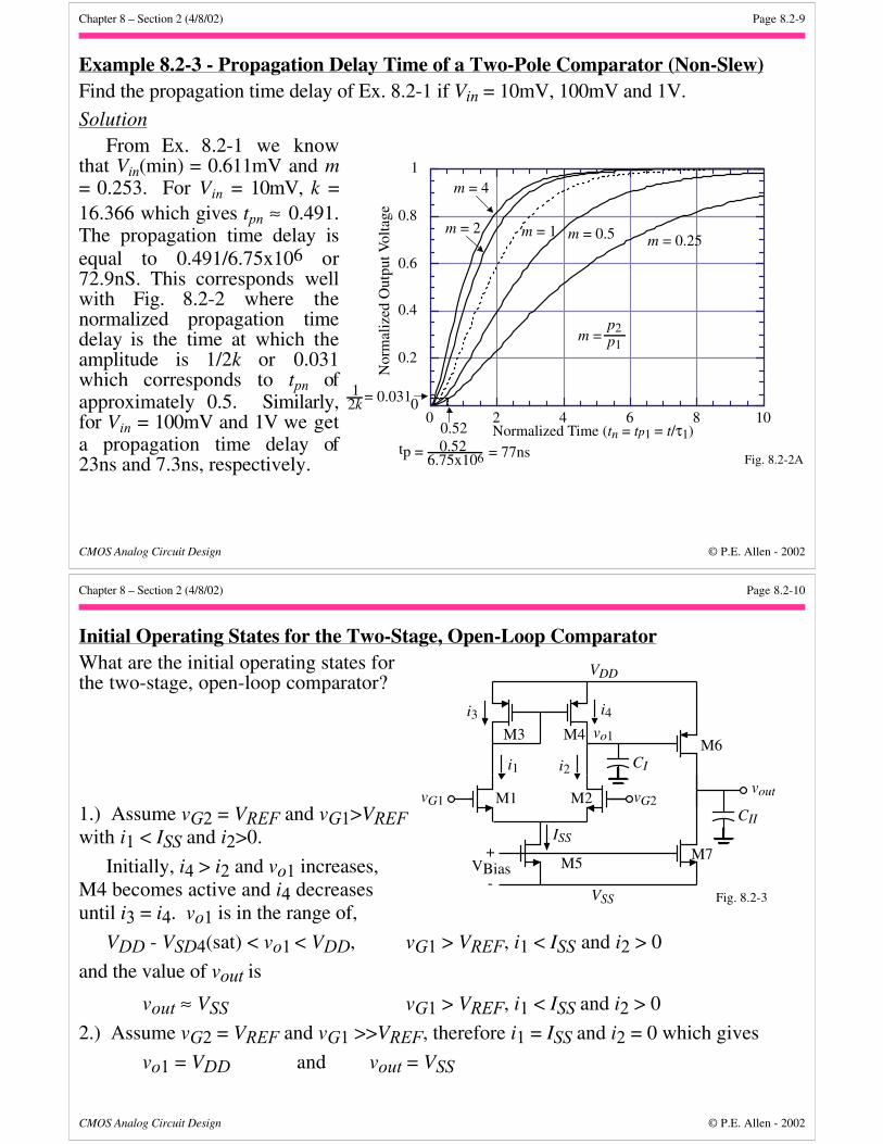
Initial Operating States for the Two-Stage, Open-Loop ComparatorWhat are the initial operating states forthe two-stage, open-loop comparator?
1.) Assume vG2 = VREF and vG1>VREFwith i1 < ISS and i2>0.
Initially, i4 > i2 and vo1 increases,M4 becomes active and i4 decreasesuntil i3 = i4. vo1 is in the range of,
VDD - VSD4(sat) < vo1 < VDD, vG1 > VREF, i1 < ISS and i2 > 0
and the value of vout is
vout ≈ VSS vG1 > VREF, i1 < ISS and i2 > 0
2.) Assume vG2 = VREF and vG1 >>VREF, therefore i1 = ISS and i2 = 0 which gives
vo1 = VDD and vout = VSS
vG1 M1 M2
M3 M4
M5
M6
M7
vout
VDD
VSS
VBias+
-
CII
Fig. 8.2-3
vG2
i1 i2 CI
ISS
vo1
i4i3
Chapter 8 – Section 2 (4/8/02) Page 8.2-11
CMOS Analog Circuit Design © P.E. Allen - 2002
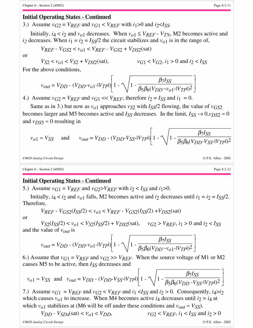
Initial Operating States - Continued3.) Assume vG2 = VREF and vG1 < VREF with i1>0 and i2<ISS.
Initially, i4 < i2 and vo1 decreases. When vo1 ≤ VREF - VTN, M2 becomes active andi2 decreases. When i1 = i2 = ISS/2 the circuit stabilizes and vo1 is in the range of,
VREF - VGS2 < vo1 < VREF - VGS2 + VDS2(sat)or
VS2 < vo1 < VS2 + VDS2(sat), vG1 < VG2, i1 > 0 and i2 < ISSFor the above conditions,
vout = VDD - (VDD-vo1-|VTP|)
1 - 1 - β7ISS
β5β6(VDD˚-vo1-|VTP|)2
4.) Assume vG2 = VREF and vG1 << VREF, therefore i2 = ISS and i1 = 0.
Same as in 3.) but now as vo1 approaches vS2 with ISS/2 flowing, the value of vGS2becomes larger and M5 becomes active and ISS decreases. In the limit, ISS → 0,vDS2 ≈ 0and vDS5 ≈ 0 resulting in
vo1 ≈ VSS and vout = VDD - (VDD-VSS-|VTP|)1 - 1 -
β7ISS
β5β6(VDD-VSS-|VTP|)2
Chapter 8 – Section 2 (4/8/02) Page 8.2-12
CMOS Analog Circuit Design © P.E. Allen - 2002
Initial Operating States - Continued5.) Assume vG1 = VREF and vG2>VREF with i2 < ISS and i1>0.
Initially, i4 < i2 and vo1 falls, M2 becomes active and i2 decreases until i1 = i2 = ISS/2.Therefore,
VREF - VGS2(ISS/2) < vo1 < VREF - VGS2(ISS/2) +VDS2(sat)or
VS2(ISS/2) < vo1 < VS2(ISS/2) + VDS2(sat), vG2 > VREF, i1 > 0 and i2 < ISSand the value of vout is
vout = VDD - (VDD-vo1-|VTP|)
1 - 1 - β7ISS
β5β6(VDD˚-vo1-|VTP|)2
6.) Assume that vG1 = VREF and vG2 >> VREF. When the source voltage of M1 or M2causes M5 to be active, then ISS decreases and
vo1 ≈ VSS and vout = VDD - (VDD-VSS-|VTP|)
1 - 1 - β7ISS
β5β6(VDD -VSS-|VTP|)2
7.) Assume vG1 = VREF and vG2 < VREF and i1 <ISS and i2 > 0. Consequently, i4>i2which causes vo1 to increase. When M4 becomes active i4 decreases until i2 = i4 atwhich vo1 stabilizes at (M6 will be off under these conditions and vout ≈ VSS).
VDD - VSD4(sat) < vo1 < VDD, vG2 < VREF, i1 < ISS and i2 > 0
Chapter 8 – Section 2 (4/8/02) Page 8.2-13
CMOS Analog Circuit Design © P.E. Allen - 2002
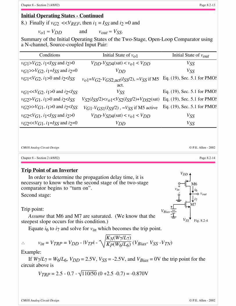
Initial Operating States - Continued8.) Finally if vG2 <<VREF, then i1 = ISS and i2 =0 and
vo1 ≈ VDD and vout ≈ VSS.
Summary of the Initial Operating States of the Two-Stage, Open-Loop Comparator usinga N-channel, Source-coupled Input Pair:
Conditions Initial State of vo1 Initial State of voutvG1>VG2, i1<ISS and i2>0 VDD-VSD4(sat) < vo1 < VDD VSSvG1>>VG2, i1=ISS and i2=0 VDD VSSvG1<VG2, i1>0 and i2<ISS vo1=VG2-VGS2,act(ISS/2), ≈VSS if M5
act.
Eq. (19), Sec. 5.1 for PMOS
vG1<<VG2, i1>0 and i2<ISS VSS Eq. (19), Sec. 5.1 for PMOS
vG2>VG1, i1>0 and i2<ISS VS2(ISS/2)<vo1<VS2(ISS/2)+VDS2(sat) Eq. (19), Sec. 5.1 for PMOS
vG2>>VG1, i1>0 and i2<ISS VG1-VGS1(ISS/2) , ≈VSS if M5 active Eq. (19), Sec. 5.1 for PMOS
vG2<VG1, i1<ISS and i2>0 VDD-VSD4(sat) < vo1 < VDD VSSvG2<<VG1, i1=ISS and i2=0 VDD VSS
Chapter 8 – Section 2 (4/8/02) Page 8.2-14
CMOS Analog Circuit Design © P.E. Allen - 2002
Trip Point of an InverterIn order to determine the propagation delay time, it is
necessary to know when the second stage of the two-stagecomparator begins to “turn on”.Second stage:
Trip point:Assume that M6 and M7 are saturated. (We know that the
steepest slope occurs for this condition.)Equate i6 to i7 and solve for vin which becomes the trip point.
∴ vin = VTRP = VDD - |VTP| - KN(W7/L7)KP(W6/L6) (VBias- VSS -VTN)
Example:If W7/L7 = W6/L6, VDD = 2.5V, VSS = -2.5V, and VBias = 0V the trip point for the
circuit above is
VTRP = 2.5 - 0.7 - 110/50 (0 +2.5 -0.7) = -0.870V
vin
M6
M7
vout
VDD
VSS
+
-i6
i7
Fig. 8.2-4
VBias
Chapter 8 – Section 2 (4/8/02) Page 8.2-15
CMOS Analog Circuit Design © P.E. Allen - 2002
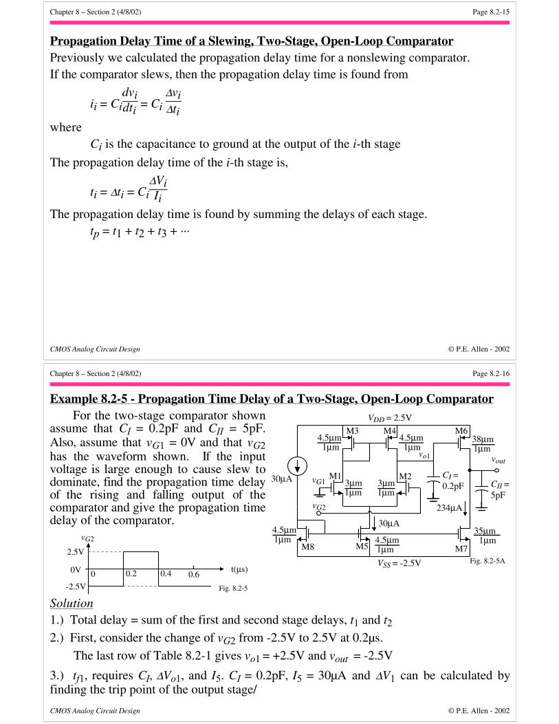
Propagation Delay Time of a Slewing, Two-Stage, Open-Loop ComparatorPreviously we calculated the propagation delay time for a nonslewing comparator.If the comparator slews, then the propagation delay time is found from
ii = Cidvidti = Ci
∆vi∆ti
whereCi is the capacitance to ground at the output of the i-th stage
The propagation delay time of the i-th stage is,
ti = ∆ti = Ci∆ViIi
The propagation delay time is found by summing the delays of each stage.tp = t1 + t2 + t3 + ···
Chapter 8 – Section 2 (4/8/02) Page 8.2-16
CMOS Analog Circuit Design © P.E. Allen - 2002
Example 8.2-5 - Propagation Time Delay of a Two-Stage, Open-Loop ComparatorFor the two-stage comparator shown
assume that CI = 0.2pF and CII = 5pF.Also, assume that vG1 = 0V and that vG2has the waveform shown. If the inputvoltage is large enough to cause slew todominate, find the propagation time delayof the rising and falling output of thecomparator and give the propagation timedelay of the comparator.
2.5V
-2.5V
t(µs)0V 0.2 0.4 0.60
Fig. 8.2-5
vG2
Solution1.) Total delay = sum of the first and second stage delays, t1 and t22.) First, consider the change of vG2 from -2.5V to 2.5V at 0.2µs.
The last row of Table 8.2-1 gives vo1 = +2.5V and vout = -2.5V
3.) tf1, requires CI, ∆Vo1, and I5. CI = 0.2pF, I5 = 30µA and ∆V1 can be calculated byfinding the trip point of the output stage/
vG2
M1 M2
M3 M4
M5
M6
M7
vout
VDD = 2.5V
VSS = -2.5V
CII =5pF
3µm1µm
3µm1µm
4.5µm1µm
4.5µm1µm
M84.5µm1µm
30µA
4.5µm1µm
35µm1µm
38µm1µm
30µA
234µA
Fig. 8.2-5A
CI =0.2pF
vo1
vG1
Chapter 8 – Section 2 (4/8/02) Page 8.2-17
CMOS Analog Circuit Design © P.E. Allen - 2002
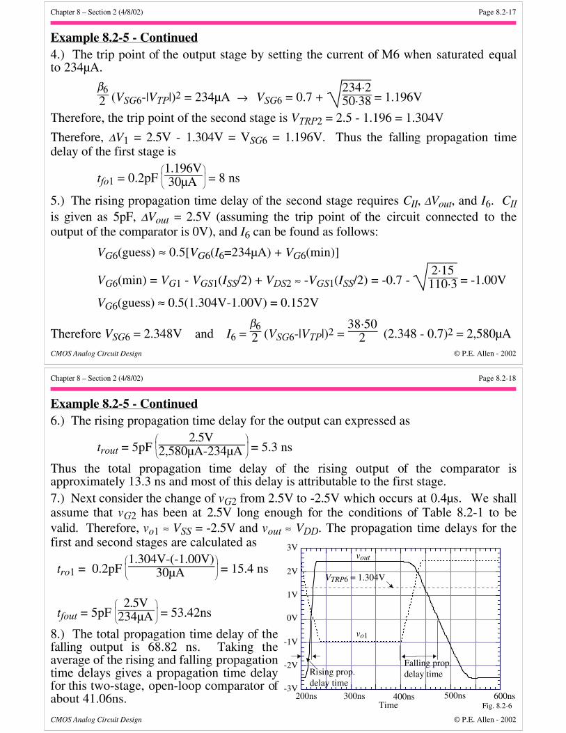
Example 8.2-5 - Continued4.) The trip point of the output stage by setting the current of M6 when saturated equalto 234µA.
β62 (VSG6-|VTP|)2 = 234µA → VSG6 = 0.7 +
234·250·38 = 1.196V
Therefore, the trip point of the second stage is VTRP2 = 2.5 - 1.196 = 1.304V
Therefore, ∆V1 = 2.5V - 1.304V = VSG6 = 1.196V. Thus the falling propagation timedelay of the first stage is
tfo1 = 0.2pF
1.196V
30µA = 8 ns
5.) The rising propagation time delay of the second stage requires CII, ∆Vout, and I6. CIIis given as 5pF, ∆Vout = 2.5V (assuming the trip point of the circuit connected to theoutput of the comparator is 0V), and I6 can be found as follows:
VG6(guess) ≈ 0.5[VG6(I6=234µA) + VG6(min)]
VG6(min) = VG1 - VGS1(ISS/2) + VDS2 ≈ -VGS1(ISS/2) = -0.7 - 2·15
110·3 = -1.00V
VG6(guess) ≈ 0.5(1.304V-1.00V) = 0.152V
Therefore VSG6 = 2.348V and I6 = β62 (VSG6-|VTP|)2 =
38·502 (2.348 - 0.7)2 = 2,580µA
Chapter 8 – Section 2 (4/8/02) Page 8.2-18
CMOS Analog Circuit Design © P.E. Allen - 2002
Example 8.2-5 - Continued6.) The rising propagation time delay for the output can expressed as
trout = 5pF
2.5V
2,580µA-234µA = 5.3 ns
Thus the total propagation time delay of the rising output of the comparator isapproximately 13.3 ns and most of this delay is attributable to the first stage.7.) Next consider the change of vG2 from 2.5V to -2.5V which occurs at 0.4µs. We shallassume that vG2 has been at 2.5V long enough for the conditions of Table 8.2-1 to bevalid. Therefore, vo1 ≈ VSS = -2.5V and vout ≈ VDD. The propagation time delays for thefirst and second stages are calculated as
tro1 = 0.2pF
1.304V-(-1.00V)
30µA = 15.4 ns
tfout = 5pF
2.5V
234µA = 53.42ns
8.) The total propagation time delay of thefalling output is 68.82 ns. Taking theaverage of the rising and falling propagationtime delays gives a propagation time delayfor this two-stage, open-loop comparator ofabout 41.06ns.
-3V
-2V
-1V
0V
1V
2V
3V
200ns 300ns 400ns 500ns 600ns
vout
vo1
Time Fig. 8.2-6
VTRP6 = 1.304V
Falling prop.delay timeRising prop.
delay time
Chapter 8 – Section 2 (4/8/02) Page 8.2-19
CMOS Analog Circuit Design © P.E. Allen - 2002
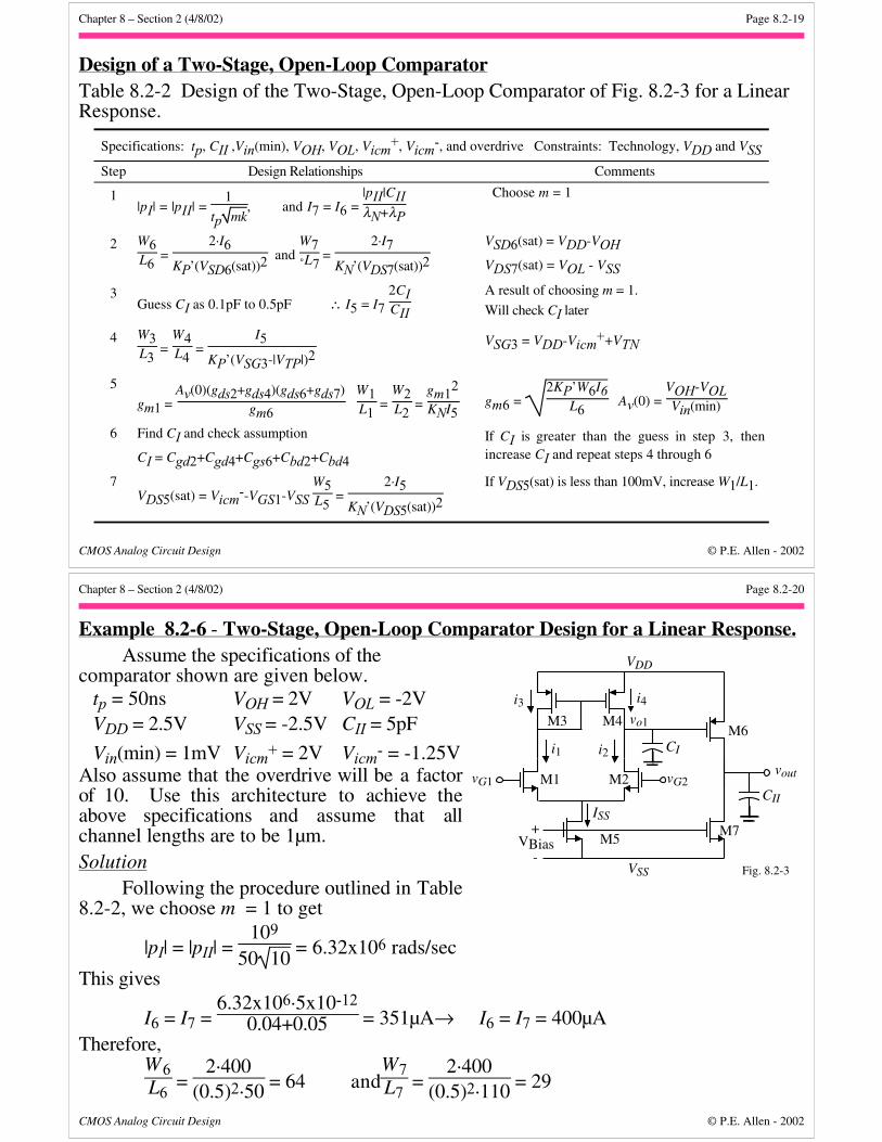
Design of a Two-Stage, Open-Loop ComparatorTable 8.2-2 Design of the Two-Stage, Open-Loop Comparator of Fig. 8.2-3 for a LinearResponse.
Specifications: tp, CII ,Vin(min), VOH, VOL, Vicm+, Vicm
-, and overdrive Constraints: Technology, VDD and VSS
Step Design Relationships Comments
1|pI| = |pII| =
1
tp mk, and I7 = I6 =
|pII|CIIλN+λP
Choose m = 1
2 W6L6
= 2·I6
KP’(VSD6(sat))2 and
W7˚L7
= 2·I7
KN’(VDS7(sat))2
VSD6(sat) = VDD-VOH
VDS7(sat) = VOL - VSS
3Guess CI as 0.1pF to 0.5pF ∴ I5 = I7
2CICII
A result of choosing m = 1.
Will check CI later
4 W3L3
= W4L4
= I5
KP’(VSG3-|VTP|)2
VSG3 = VDD-Vicm++VTN
5
gm1 = Av(0)(gds2+gds4)(gds6+gds7)
gm6
W1L1
= W2L2
= gm1
2
KNI5 gm6 =
2KP’W6I6L6
Av(0) = VOH-VOLVin(min)
6 Find CI and check assumption
CI = Cgd2+Cgd4+Cgs6+Cbd2+Cbd4
If CI is greater than the guess in step 3, thenincrease CI and repeat steps 4 through 6
7VDS5(sat) = Vicm
--VGS1-VSS W5L5
= 2·I5
KN’(VDS5(sat))2
If VDS5(sat) is less than 100mV, increase W1/L1.
Chapter 8 – Section 2 (4/8/02) Page 8.2-20
CMOS Analog Circuit Design © P.E. Allen - 2002
Example 8.2-6 - Two-Stage, Open-Loop Comparator Design for a Linear Response.Assume the specifications of the
comparator shown are given below.tp = 50ns VOH = 2V VOL = -2VVDD = 2.5V VSS = -2.5V CII = 5pF
Vin(min) = 1mV Vicm+ = 2V Vicm- = -1.25VAlso assume that the overdrive will be a factorof 10. Use this architecture to achieve theabove specifications and assume that allchannel lengths are to be 1µm.Solution
Following the procedure outlined in Table8.2-2, we choose m = 1 to get
|pI| = |pII| = 109
50 10 = 6.32x10⁶ rads/sec
This gives
I6 = I7 = 6.32x106·5x10-12
0.04+0.05 = 351µA→ I6 = I7 = 400µATherefore,
W6L6
= 2·400
(0.5)2·50 = 64 andW7L7
= 2·400
(0.5)2·110 = 29
vG1 M1 M2
M3 M4
M5
M6
M7
vout
VDD
VSS
VBias+
-
CII
Fig. 8.2-3
vG2
i1 i2 CI
ISS
vo1
i4i3
Chapter 8 – Section 2 (4/8/02) Page 8.2-21
CMOS Analog Circuit Design © P.E. Allen - 2002
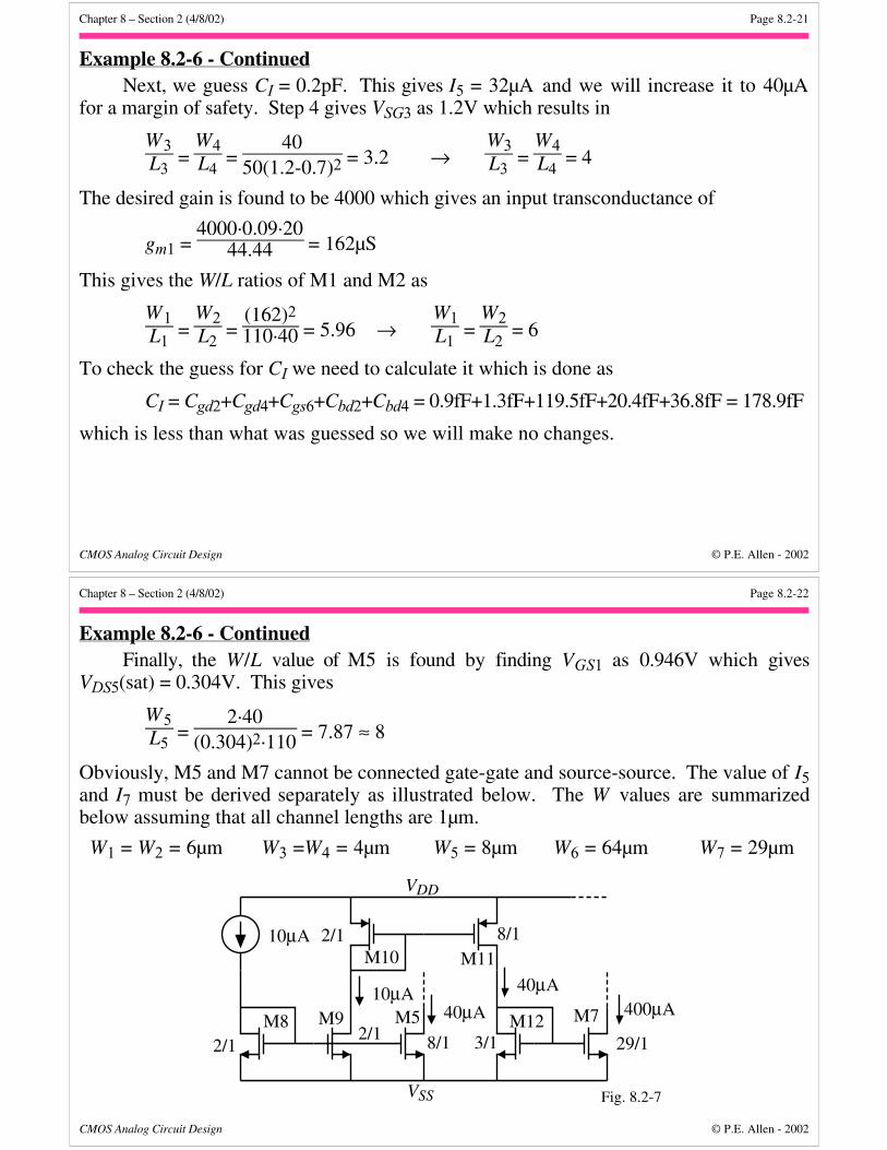
Example 8.2-6 - ContinuedNext, we guess CI = 0.2pF. This gives I5 = 32µA and we will increase it to 40µA
for a margin of safety. Step 4 gives VSG3 as 1.2V which results in
W3L3
= W4L4
= 40
50(1.2-0.7)2 = 3.2 → W3L3
= W4L4
= 4
The desired gain is found to be 4000 which gives an input transconductance of
gm1 = 4000·0.09·20
44.44 = 162µS
This gives the W/L ratios of M1 and M2 as
W1L1
= W2L2
= (162)2
110·40 = 5.96 → W1L1
= W2L2
= 6
To check the guess for CI we need to calculate it which is done as
CI = Cgd2+Cgd4+Cgs6+Cbd2+Cbd4 = 0.9fF+1.3fF+119.5fF+20.4fF+36.8fF = 178.9fF
which is less than what was guessed so we will make no changes.
Chapter 8 – Section 2 (4/8/02) Page 8.2-22
CMOS Analog Circuit Design © P.E. Allen - 2002
Example 8.2-6 - ContinuedFinally, the W/L value of M5 is found by finding VGS1 as 0.946V which gives
VDS5(sat) = 0.304V. This gives
W5L5
= 2·40
(0.304)2·110 = 7.87 ≈ 8
Obviously, M5 and M7 cannot be connected gate-gate and source-source. The value of I5and I7 must be derived separately as illustrated below. The W values are summarizedbelow assuming that all channel lengths are 1µm.
W1 = W2 = 6µm W3 =W4 = 4µm W5 = 8µm W6 = 64µm W7 = 29µm
M5 M7
VSS
400µA40µA
10µA
10µA 40µA
M8 M9
M10 M11
M128/12/1
2/1
2/1
29/1
8/1
3/1
Fig. 8.2-7
VDD
Chapter 8 – Section 2 (4/8/02) Page 8.2-23
CMOS Analog Circuit Design © P.E. Allen - 2002
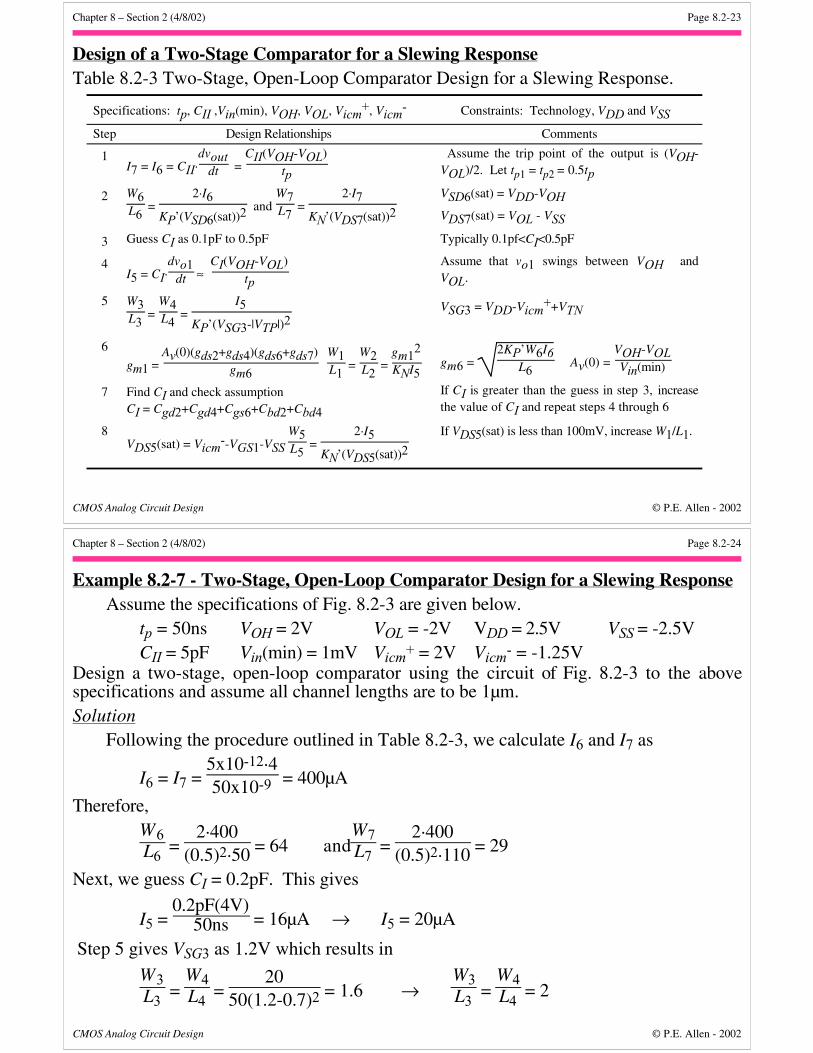
Design of a Two-Stage Comparator for a Slewing ResponseTable 8.2-3 Two-Stage, Open-Loop Comparator Design for a Slewing Response.
Specifications: tp, CII ,Vin(min), VOH, VOL, Vicm+, Vicm
- Constraints: Technology, VDD and VSS
Step Design Relationships Comments
1I7 = I6 = CII·
dvoutdt =
CII(VOH-VOL)tp
Assume the trip point of the output is (VOH-VOL)/2. Let tp1 = tp2 = 0.5tp
2 W6L6
= 2·I6
KP’(VSD6(sat))2 and
W7L7
= 2·I7
KN’(VDS7(sat))2
VSD6(sat) = VDD-VOH
VDS7(sat) = VOL - VSS
3 Guess CI as 0.1pF to 0.5pF Typically 0.1pf<CI<0.5pF
4I5 = CI·
dvo1dt ≈
CI(VOH-VOL)tp
Assume that vo1 swings between VOH andVOL.
5 W3L3
= W4L4
= I5
KP’(VSG3-|VTP|)2
VSG3 = VDD-Vicm++VTN
6
gm1 = Av(0)(gds2+gds4)(gds6+gds7)
gm6
W1L1
= W2L2
= gm1
2
KNI5 gm6 =
2KP’W6I6L6
Av(0) = VOH-VOLVin(min)
7 Find CI and check assumptionCI = Cgd2+Cgd4+Cgs6+Cbd2+Cbd4
If CI is greater than the guess in step 3, increasethe value of CI and repeat steps 4 through 6
8VDS5(sat) = Vicm
--VGS1-VSS W5L5
= 2·I5
KN’(VDS5(sat))2
If VDS5(sat) is less than 100mV, increase W1/L1.
Chapter 8 – Section 2 (4/8/02) Page 8.2-24
CMOS Analog Circuit Design © P.E. Allen - 2002
Example 8.2-7 - Two-Stage, Open-Loop Comparator Design for a Slewing ResponseAssume the specifications of Fig. 8.2-3 are given below.
tp = 50ns VOH = 2V VOL = -2V VDD = 2.5V VSS = -2.5VCII = 5pF Vin(min) = 1mV Vicm+ = 2V Vicm- = -1.25V
Design a two-stage, open-loop comparator using the circuit of Fig. 8.2-3 to the abovespecifications and assume all channel lengths are to be 1µm.Solution
Following the procedure outlined in Table 8.2-3, we calculate I6 and I7 as
I6 = I7 = 5x10-12·450x10-9 = 400µA
Therefore,W6L6
= 2·400
(0.5)2·50 = 64 andW7L7
= 2·400
(0.5)2·110 = 29
Next, we guess CI = 0.2pF. This gives
I5 = 0.2pF(4V)
50ns = 16µA → I5 = 20µA
Step 5 gives VSG3 as 1.2V which results in
W3L3
= W4L4
= 20
50(1.2-0.7)2 = 1.6 → W3L3
= W4L4
= 2
Chapter 8 – Section 2 (4/8/02) Page 8.2-25
CMOS Analog Circuit Design © P.E. Allen - 2002
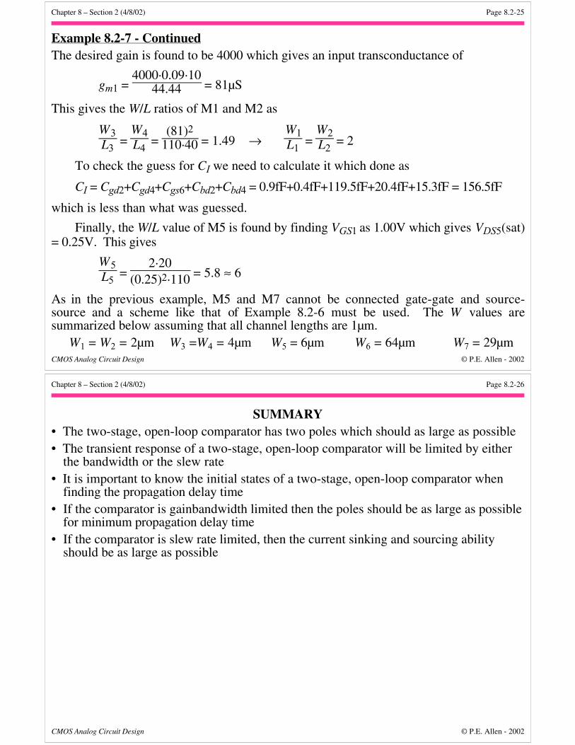
Example 8.2-7 - ContinuedThe desired gain is found to be 4000 which gives an input transconductance of
gm1 = 4000·0.09·10
44.44 = 81µS
This gives the W/L ratios of M1 and M2 as
W3L3
= W4L4
= (81)2
110·40 = 1.49 → W1L1
= W2L2
= 2
To check the guess for CI we need to calculate it which done as
CI = Cgd2+Cgd4+Cgs6+Cbd2+Cbd4 = 0.9fF+0.4fF+119.5fF+20.4fF+15.3fF = 156.5fF
which is less than what was guessed.
Finally, the W/L value of M5 is found by finding VGS1 as 1.00V which gives VDS5(sat)= 0.25V. This gives
W5L5
= 2·20
(0.25)2·110 = 5.8 ≈ 6
As in the previous example, M5 and M7 cannot be connected gate-gate and source-source and a scheme like that of Example 8.2-6 must be used. The W values aresummarized below assuming that all channel lengths are 1µm.
W1 = W2 = 2µm W3 =W4 = 4µm W5 = 6µm W6 = 64µm W7 = 29µm
Chapter 8 – Section 2 (4/8/02) Page 8.2-26
CMOS Analog Circuit Design © P.E. Allen - 2002
SUMMARY• The two-stage, open-loop comparator has two poles which should as large as possible• The transient response of a two-stage, open-loop comparator will be limited by either
the bandwidth or the slew rate• It is important to know the initial states of a two-stage, open-loop comparator when
finding the propagation delay time• If the comparator is gainbandwidth limited then the poles should be as large as possible
for minimum propagation delay time• If the comparator is slew rate limited, then the current sinking and sourcing ability
should be as large as possible
Chapter 8 – Section 3 (4/8/02) Page 8.3-1
CMOS Analog Circuit Design © P.E. Allen - 2002
SECTION 8.3– OTHER OPEN-LOOP COMPARATORSObjectiveThe objective of this section is:1.) Show other types of continuous-time, open-loop comparatorsOutline• Push-pull comparators• Comparators that can drive large capacitors
Chapter 8 – Section 3 (4/8/02) Page 8.3-2
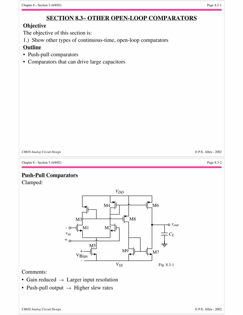
CMOS Analog Circuit Design © P.E. Allen - 2002
Push-Pull ComparatorsClamped:
-
+vin
M1 M2
M3
M4
M5
M6
vout
VDD
VSS
VBias+
-
CL
M9
M8
M7
Fig. 8.3-1
Comments:
• Gain reduced → Larger input resolution
• Push-pull output → Higher slew rates
Chapter 8 – Section 3 (4/8/02) Page 8.3-3
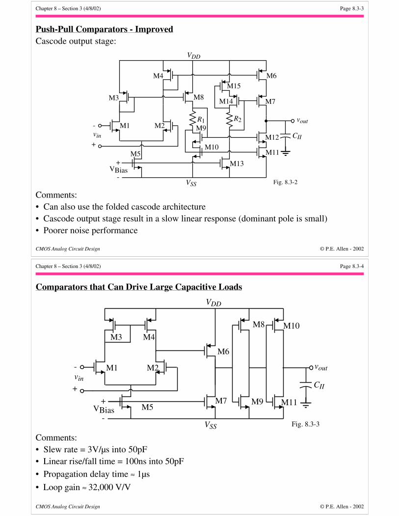
CMOS Analog Circuit Design © P.E. Allen - 2002
Push-Pull Comparators - ImprovedCascode output stage:
-
+vin
M1 M2
M3
M4
M5
M6
M11
vout
VDD
VSS
VBias+
-
CII
R1M9
M10
R2
M14
M15
M8
M12
M7
M13
Fig. 8.3-2
Comments:• Can also use the folded cascode architecture• Cascode output stage result in a slow linear response (dominant pole is small)• Poorer noise performance
Chapter 8 – Section 3 (4/8/02) Page 8.3-4
CMOS Analog Circuit Design © P.E. Allen - 2002
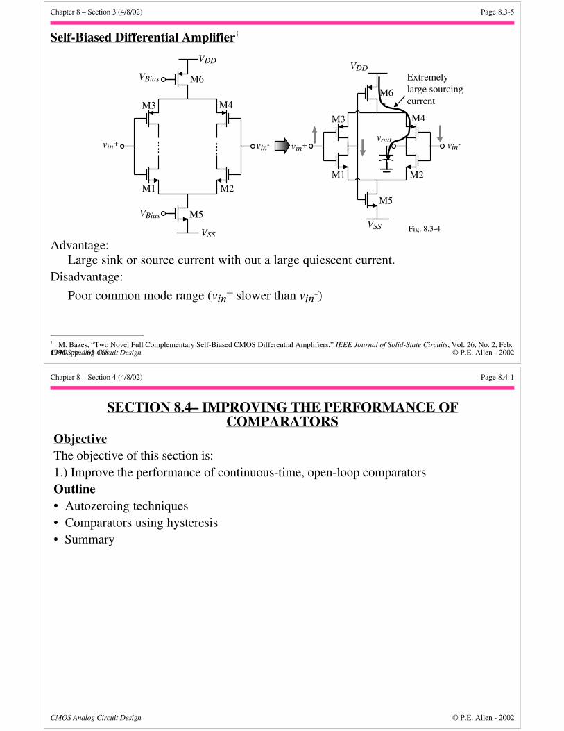
Comparators that Can Drive Large Capacitive Loads
-
+vin
M1 M2
M3 M4
M5
M6
M7
vout
VDD
VSS
VBias+
-
CII
M8
M9
M10
M11
Fig. 8.3-3
Comments:• Slew rate = 3V/µs into 50pF• Linear rise/fall time = 100ns into 50pF
• Propagation delay time ≈ 1µs
• Loop gain ≈ 32,000 V/V
Chapter 8 – Section 3 (4/8/02) Page 8.3-5
CMOS Analog Circuit Design © P.E. Allen - 2002
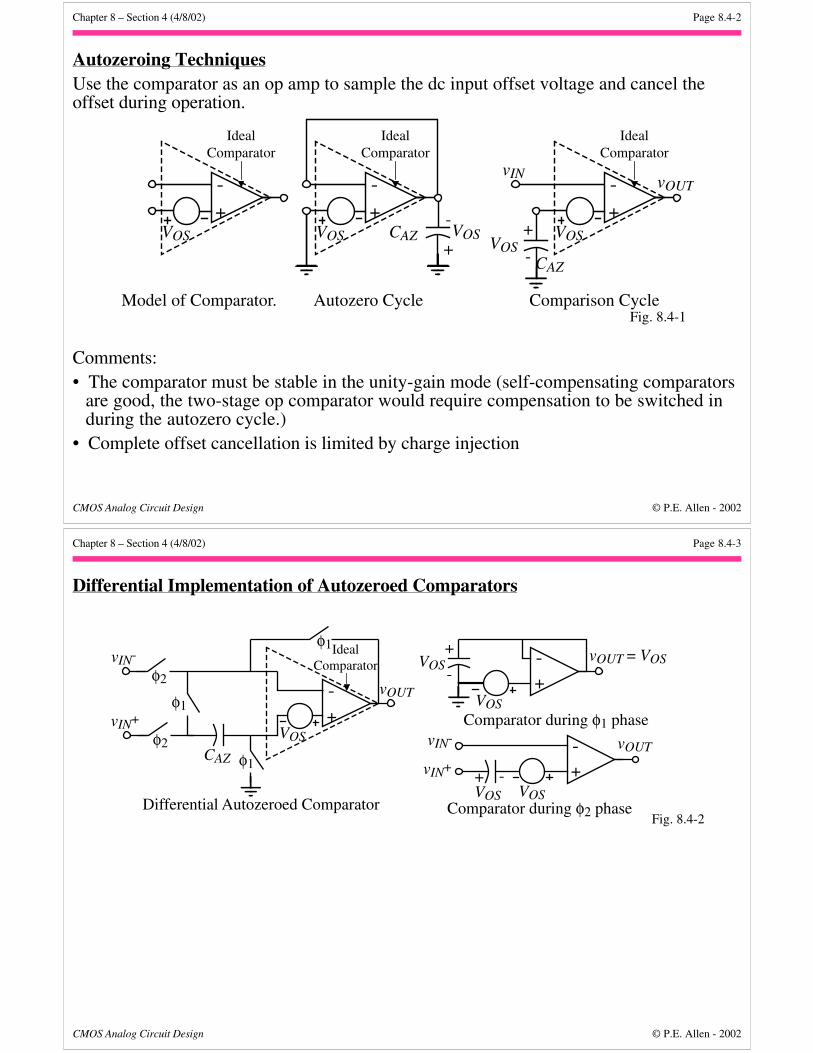
Self-Biased Differential Amplifier†
M1 M2
M3 M4
M6
M5
VDD
VSS
vin+ vin-vout
M3 M4
M6
VDD
M1 M2
M5
VSS
vin+ vin-
VBias
VBias Extremelylarge sourcingcurrent
Fig. 8.3-4
Advantage:Large sink or source current with out a large quiescent current.
Disadvantage:
Poor common mode range (vin+ slower than vin-)
† M. Bazes, “Two Novel Full Complementary Self-Biased CMOS Differential Amplifiers,” IEEE Journal of Solid-State Circuits, Vol. 26, No. 2, Feb.1991, pp. 165-168.
Chapter 8 – Section 4 (4/8/02) Page 8.4-1
CMOS Analog Circuit Design © P.E. Allen - 2002
SECTION 8.4– IMPROVING THE PERFORMANCE OFCOMPARATORS
ObjectiveThe objective of this section is:1.) Improve the performance of continuous-time, open-loop comparatorsOutline• Autozeroing techniques• Comparators using hysteresis• Summary
Chapter 8 – Section 4 (4/8/02) Page 8.4-2
CMOS Analog Circuit Design © P.E. Allen - 2002
Autozeroing TechniquesUse the comparator as an op amp to sample the dc input offset voltage and cancel theoffset during operation.
+-
VOS VOS+
-
IdealComparator
+-
VOS
IdealComparator
CAZ VOS+
-
+-
VOS
IdealComparator
CAZ
vIN vOUT
Model of Comparator. Autozero Cycle Comparison CycleFig. 8.4-1
Comments:• The comparator must be stable in the unity-gain mode (self-compensating comparators
are good, the two-stage op comparator would require compensation to be switched induring the autozero cycle.)
• Complete offset cancellation is limited by charge injection
Chapter 8 – Section 4 (4/8/02) Page 8.4-3
CMOS Analog Circuit Design © P.E. Allen - 2002
Differential Implementation of Autozeroed Comparators
VOS+
-
+-
VOS
IdealComparator
CAZ
vIN-
vOUTφ1
φ1
φ1
φ2 +-
VOS
vOUT = VOS
VOS+ -
+-
VOS
Comparator during φ1 phase
Comparator during φ2 phaseDifferential Autozeroed Comparator
vOUT
Fig. 8.4-2
vIN+
φ2
vIN+
vIN-
Chapter 8 – Section 4 (4/8/02) Page 8.4-4
CMOS Analog Circuit Design © P.E. Allen - 2002
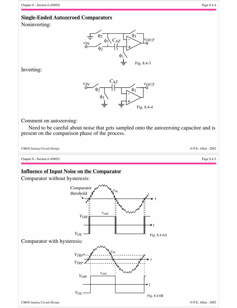
Single-Ended Autozeroed ComparatorsNoninverting:
+-φ2
φ2
φ1 CAZ
φ1
φ1vOUTvIN
Fig. 8.4-3
Inverting:
+-φ2
CAZ
φ1
φ1
vOUTvIN
Fig. 8.4-4
Comment on autozeroing:Need to be careful about noise that gets sampled onto the autozeroing capacitor and is
present on the comparison phase of the process.
Chapter 8 – Section 4 (4/8/02) Page 8.4-5
CMOS Analog Circuit Design © P.E. Allen - 2002
Influence of Input Noise on the ComparatorComparator without hysteresis:
vin
voutVOH
VOL
Comparatorthreshold
t
t
Fig. 8.4-6A
Comparator with hysteresis:
vin
voutVOH
VOL
t
t
VTRP+
VTRP-
Fig. 8.4-6B
Chapter 8 – Section 4 (4/8/02) Page 8.4-6
CMOS Analog Circuit Design © P.E. Allen - 2002
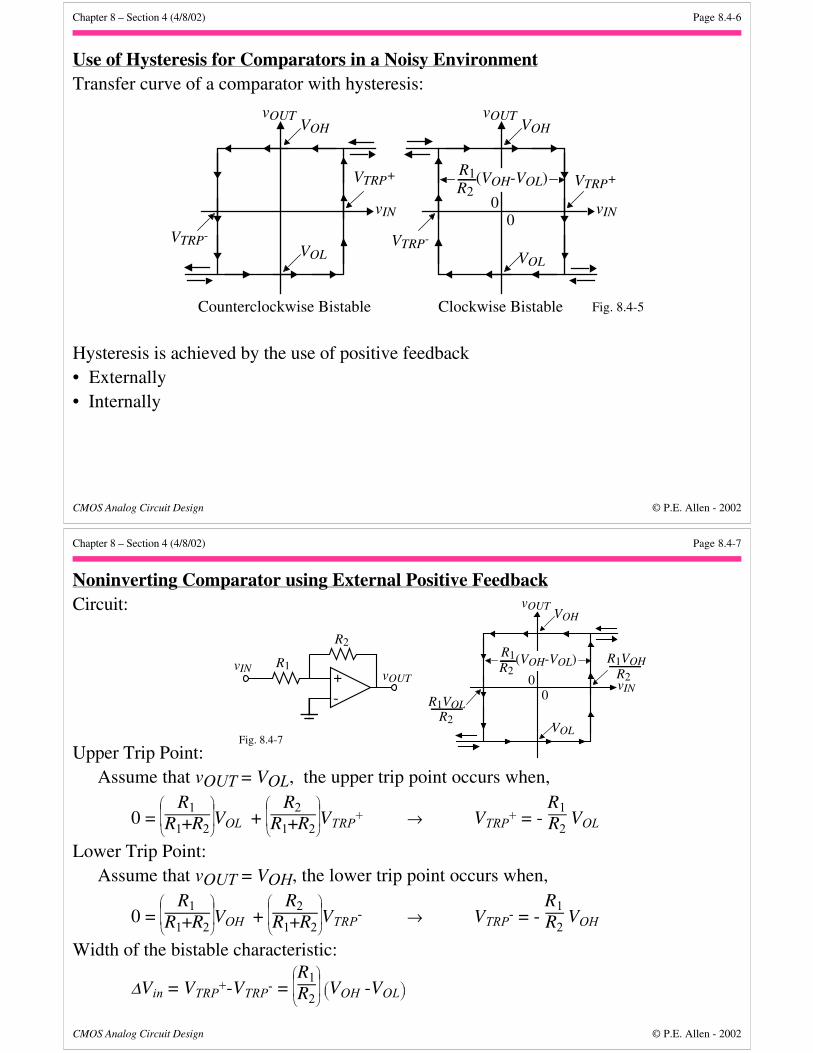
Use of Hysteresis for Comparators in a Noisy EnvironmentTransfer curve of a comparator with hysteresis:
vOUT
vIN
VTRP+
VTRP-
VOH
VOL
Fig. 8.4-5
vOUT
vIN
VOH
VOL
00
R1R2
(VOH-VOL) VTRP+
VTRP-
Counterclockwise Bistable Clockwise Bistable
Hysteresis is achieved by the use of positive feedback• Externally• Internally
Chapter 8 – Section 4 (4/8/02) Page 8.4-7
CMOS Analog Circuit Design © P.E. Allen - 2002
Noninverting Comparator using External Positive FeedbackCircuit:
Upper Trip Point:Assume that vOUT = VOL, the upper trip point occurs when,
0 =
R1
R1+R2VOL +
R2
R1+R2VTRP
+ → VTRP+ = -
R1R2
VOL
Lower Trip Point:Assume that vOUT = VOH, the lower trip point occurs when,
0 =
R1
R1+R2VOH +
R2
R1+R2VTRP
- → VTRP- = -
R1R2
VOH
Width of the bistable characteristic:
∆Vin = VTRP+-VTRP
- =
R1
R2 VOH -VOL
vOUT
vIN
VOH
VOL
+-
vOUTvIN R1
R2
R1VOHR2
R1VOLR2
Fig. 8.4-7
00
R1R2
(VOH-VOL)
Chapter 8 – Section 4 (4/8/02) Page 8.4-8
CMOS Analog Circuit Design © P.E. Allen - 2002
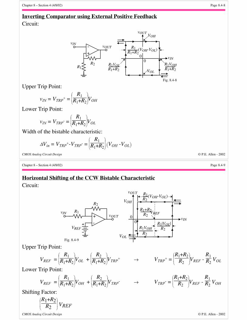
Inverting Comparator using External Positive FeedbackCircuit:
+- vOUT
vIN
R1R2
vOUT
vIN
VOH
VOL
R1VOHR1VOL
Fig. 8.4-8
00
R1R1+R2
(VOH-VOL)
R1+R2R1+R2
Upper Trip Point:
vIN = VTRP+ =
R1
R1+R2VOH
Lower Trip Point:
vIN = VTRP- =
R1
R1+R2VOL
Width of the bistable characteristic:
∆Vin = VTRP+-VTRP
- =
R1
R1+R2 VOH -VOL
Chapter 8 – Section 4 (4/8/02) Page 8.4-9
CMOS Analog Circuit Design © P.E. Allen - 2002
Horizontal Shifting of the CCW Bistable CharacteristicCircuit:
vOUT
vIN
VOH
VOL
+-
vOUTvIN R1
R2
R1VOHR2
Fig. 8.4-9
00
R1R2
(VOH-VOL)
VREFR1|VOL|
R2
R1+R2R2
VREF
Upper Trip Point:
VREF =
R1
R1+R2VOL +
R2
R1+R2VTRP
+ → VTRP+ =
R1+R2
R2VREF -
R1R2
VOL
Lower Trip Point:
VREF =
R1
R1+R2VOH +
R2
R1+R2VTRP
- → VTRP- =
R1+R2
R2VREF -
R1R2
VOH
Shifting Factor:
R1+R2
R2 VREF
Chapter 8 – Section 4 (4/8/02) Page 8.4-10
CMOS Analog Circuit Design © P.E. Allen - 2002
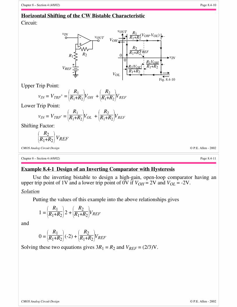
Horizontal Shifting of the CW Bistable CharacteristicCircuit:
+- vOUT
vIN
R1R2
Fig. 8.4-10
VREF
vOUT
vIN
VOH
VOL
R1|VOL|
00
R1 (VOH-VOL)
R1VOH
R1+R2
R2VREF
R1+R2
R1+R2
R1+R2
Upper Trip Point:
vIN = VTRP+ =
R1
R1+R2VOH +
R2
R1+R2VREF
Lower Trip Point:
vIN = VTRP- =
R1
R1+R2VOL +
R2
R1+R2VREF
Shifting Factor:
R2
R1+R2 VREF
Chapter 8 – Section 4 (4/8/02) Page 8.4-11
CMOS Analog Circuit Design © P.E. Allen - 2002
Example 8.4-1 Design of an Inverting Comparator with Hysteresis
Use the inverting bistable to design a high-gain, open-loop comparator having anupper trip point of 1V and a lower trip point of 0V if VOH = 2V and VOL = -2V.
Solution
Putting the values of this example into the above relationships gives
1 =
R1
R1+R2 2 +
R2
R1+R2VREF
and
0 =
R1
R1+R2 (-2) +
R2
R1+R2VREF
Solving these two equations gives 3R1 = R2 and VREF = (2/3)V.
Chapter 8 – Section 4 (4/8/02) Page 8.4-12
CMOS Analog Circuit Design © P.E. Allen - 2002
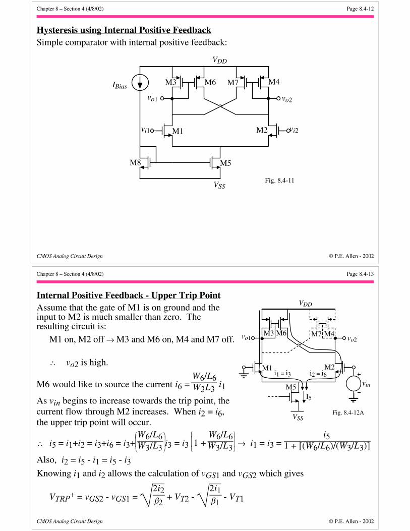
Hysteresis using Internal Positive FeedbackSimple comparator with internal positive feedback:
VSS
IBias
vo1 vo2
vi1 vi2M1 M2
M3 M4M6 M7
M5M8
VDD
Fig. 8.4-11
Chapter 8 – Section 4 (4/8/02) Page 8.4-13
CMOS Analog Circuit Design © P.E. Allen - 2002
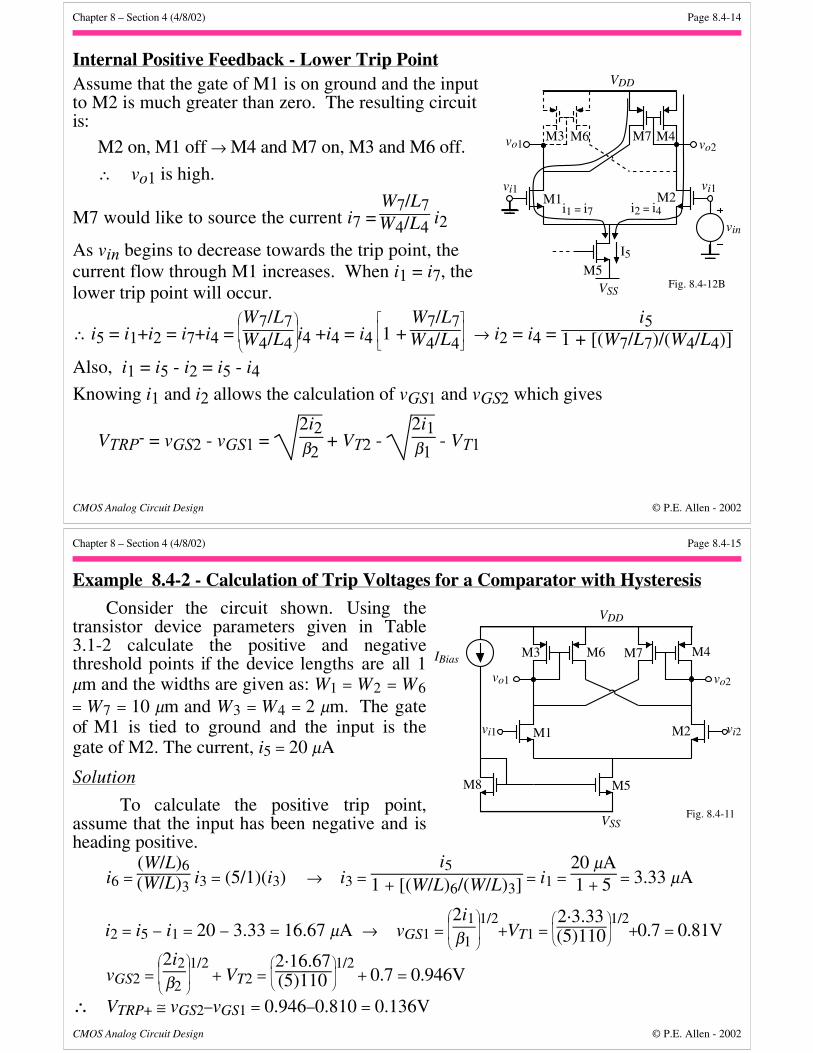
Internal Positive Feedback - Upper Trip PointAssume that the gate of M1 is on ground and theinput to M2 is much smaller than zero. Theresulting circuit is:
M1 on, M2 off → M3 and M6 on, M4 and M7 off.
∴ vo2 is high.
M6 would like to source the current i6 = W6/L6W3L3 i1
As vin begins to increase towards the trip point, thecurrent flow through M2 increases. When i2 = i6,the upper trip point will occur.
∴ i5 = i1+i2 = i3+i6 = i3+
W6/L6
W3/L3 i3 = i3
1 + W6/L6W3/L3 → i1 = i3 =
i51 + [(W6/L6)/(W3/L3)]
Also, i2 = i5 - i1 = i5 - i3Knowing i1 and i2 allows the calculation of vGS1 and vGS2 which gives
VTRP+ = vGS2 - vGS1 = 2i2β2
+ VT2 - 2i1β1
- VT1
VSS
vo1 vo2
M1 M2
M3 M4M6 M7
M5
VDD
Fig. 8.4-12A
I5
i1 = i3
vin
i2 = i6
Chapter 8 – Section 4 (4/8/02) Page 8.4-14
CMOS Analog Circuit Design © P.E. Allen - 2002
Internal Positive Feedback - Lower Trip PointAssume that the gate of M1 is on ground and the inputto M2 is much greater than zero. The resulting circuitis:
M2 on, M1 off → M4 and M7 on, M3 and M6 off.
∴ vo1 is high.
M7 would like to source the current i7 = W7/L7W4/L4 i2
As vin begins to decrease towards the trip point, thecurrent flow through M1 increases. When i1 = i7, thelower trip point will occur.
∴ i5 = i1+i2 = i7+i4 =
W7/L7
W4/L4 i4 +i4 = i4
1 + W7/L7W4/L4 → i2 = i4 =
i51 + [(W7/L7)/(W4/L4)]
Also, i1 = i5 - i2 = i5 - i4Knowing i1 and i2 allows the calculation of vGS1 and vGS2 which gives
VTRP- = vGS2 - vGS1 = 2i2β2
+ VT2 - 2i1β1
- VT1
Fig. 8.4-12BVSS
vo1 vo2
vi1M1 M2
M3 M4M6 M7
M5
VDD
I5
i2 = i4
vi1
i1 = i7
vin
Chapter 8 – Section 4 (4/8/02) Page 8.4-15
CMOS Analog Circuit Design © P.E. Allen - 2002
Example 8.4-2 - Calculation of Trip Voltages for a Comparator with Hysteresis
Consider the circuit shown. Using thetransistor device parameters given in Table3.1-2 calculate the positive and negativethreshold points if the device lengths are all 1µm and the widths are given as: W1 = W2 = W6= W7 = 10 µm and W3 = W4 = 2 µm. The gateof M1 is tied to ground and the input is thegate of M2. The current, i5 = 20 µA
Solution
To calculate the positive trip point,assume that the input has been negative and isheading positive.
i6 = (W/L)6(W/L)3
i3 = (5/1)(i3) → i3 = i5
1 + [(W/L)6/(W/L)3] = i1 = 20 µA1 + 5 = 3.33 µA
i2 = i5 − i1 = 20 − 3.33 = 16.67 µA → vGS1 =
2i1
β1
1/2+VT1 =
2·3.33
(5)1101/2
+0.7 = 0.81V
vGS2 =
2i2
β2
1/2 + VT2 =
2·16.67
(5)1101/2
+ 0.7 = 0.946V
∴ VTRP+ ≅ vGS2−vGS1 = 0.946−0.810 = 0.136V
VSS
IBias
vo1 vo2
vi1 vi2M1 M2
M3 M4M6 M7
M5M8
VDD
Fig. 8.4-11
Chapter 8 – Section 4 (4/8/02) Page 8.4-16
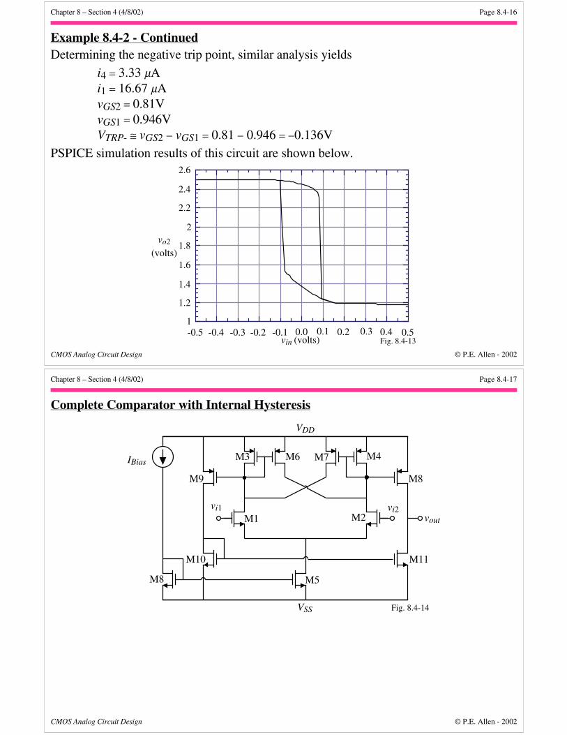
CMOS Analog Circuit Design © P.E. Allen - 2002
Example 8.4-2 - ContinuedDetermining the negative trip point, similar analysis yields
i4 = 3.33 µAi1 = 16.67 µAvGS2 = 0.81VvGS1 = 0.946VVTRP- ≅ vGS2 − vGS1 = 0.81 − 0.946 = −0.136V
PSPICE simulation results of this circuit are shown below.
1
1.2
1.4
1.6
1.8
2
2.2
2.4
2.6
-0.5 -0.4 -0.3 -0.2 -0.1 0.0 0.1 0.2 0.3 0.4 0.5
vo2
(volts)
vin (volts) Fig. 8.4-13
Chapter 8 – Section 4 (4/8/02) Page 8.4-17
CMOS Analog Circuit Design © P.E. Allen - 2002
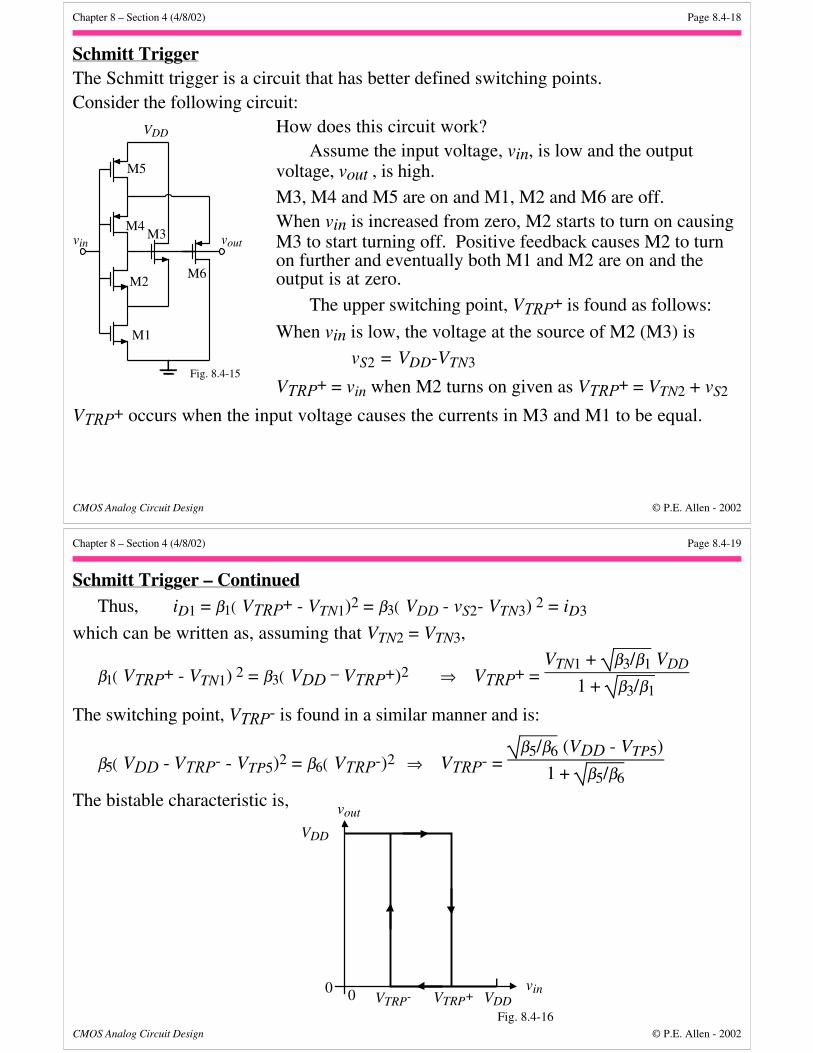
Complete Comparator with Internal Hysteresis
VSS
IBias
vout
vi1 vi2M1 M2
M3 M4M6 M7
M5M8
VDD
Fig. 8.4-14
M8M9
M10 M11
Chapter 8 – Section 4 (4/8/02) Page 8.4-18
CMOS Analog Circuit Design © P.E. Allen - 2002
Schmitt TriggerThe Schmitt trigger is a circuit that has better defined switching points.Consider the following circuit:
How does this circuit work?Assume the input voltage, vin, is low and the output
voltage, vout , is high.
M3, M4 and M5 are on and M1, M2 and M6 are off.When vin is increased from zero, M2 starts to turn on causingM3 to start turning off. Positive feedback causes M2 to turnon further and eventually both M1 and M2 are on and theoutput is at zero.
The upper switching point, VTRP+ is found as follows:
When vin is low, the voltage at the source of M2 (M3) is
vS2 = VDD-VTN3
VTRP+ = vin when M2 turns on given as VTRP+ = VTN2 + vS2
VTRP+ occurs when the input voltage causes the currents in M3 and M1 to be equal.
vin
M1
M2
M3M4
M5
M6
vout
VDD
Fig. 8.4-15
Chapter 8 – Section 4 (4/8/02) Page 8.4-19
CMOS Analog Circuit Design © P.E. Allen - 2002
Schmitt Trigger – ContinuedThus, iD1 = β1( VTRP+ - VTN1)2 = β3( VDD - vS2- VTN3) 2 = iD3
which can be written as, assuming that VTN2 = VTN3,
β1( VTRP+ - VTN1) 2 = β3( VDD – VTRP+)2 ⇒ VTRP+ = VTN1 + β3/β1 VDD
1 + β3/β1
The switching point, VTRP- is found in a similar manner and is:
β5( VDD - VTRP- - VTP5)2 = β6( VTRP-)2 ⇒ VTRP- = β5/β6 (VDD - VTP5)
1 + β5/β6
The bistable characteristic is,
vin
vout
VDD
VDD0 0 VTRP- VTRP+
Fig. 8.4-16
Chapter 8 – Section 4 (4/8/02) Page 8.4-20
CMOS Analog Circuit Design © P.E. Allen - 2002
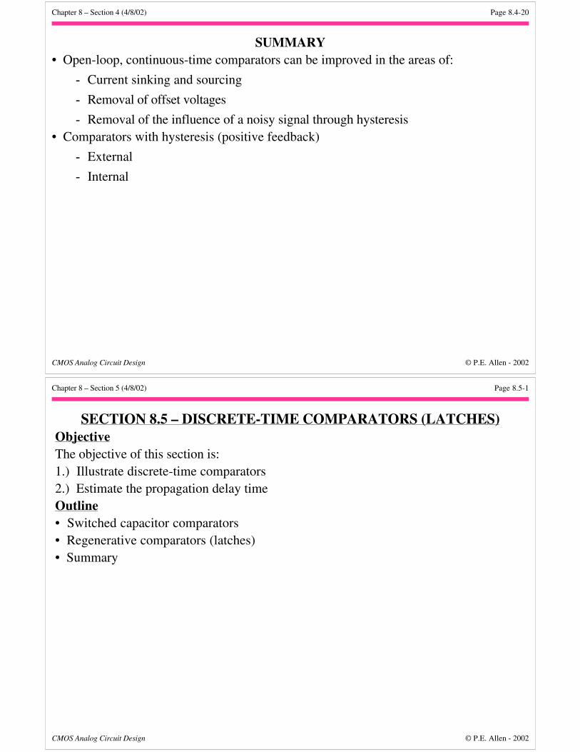
SUMMARY• Open-loop, continuous-time comparators can be improved in the areas of:
- Current sinking and sourcing
- Removal of offset voltages
- Removal of the influence of a noisy signal through hysteresis• Comparators with hysteresis (positive feedback)
- External
- Internal
Chapter 8 – Section 5 (4/8/02) Page 8.5-1
CMOS Analog Circuit Design © P.E. Allen - 2002
SECTION 8.5 – DISCRETE-TIME COMPARATORS (LATCHES)ObjectiveThe objective of this section is:1.) Illustrate discrete-time comparators2.) Estimate the propagation delay timeOutline• Switched capacitor comparators• Regenerative comparators (latches)• Summary
Chapter 8 – Section 5 (4/8/02) Page 8.5-2
CMOS Analog Circuit Design © P.E. Allen - 2002
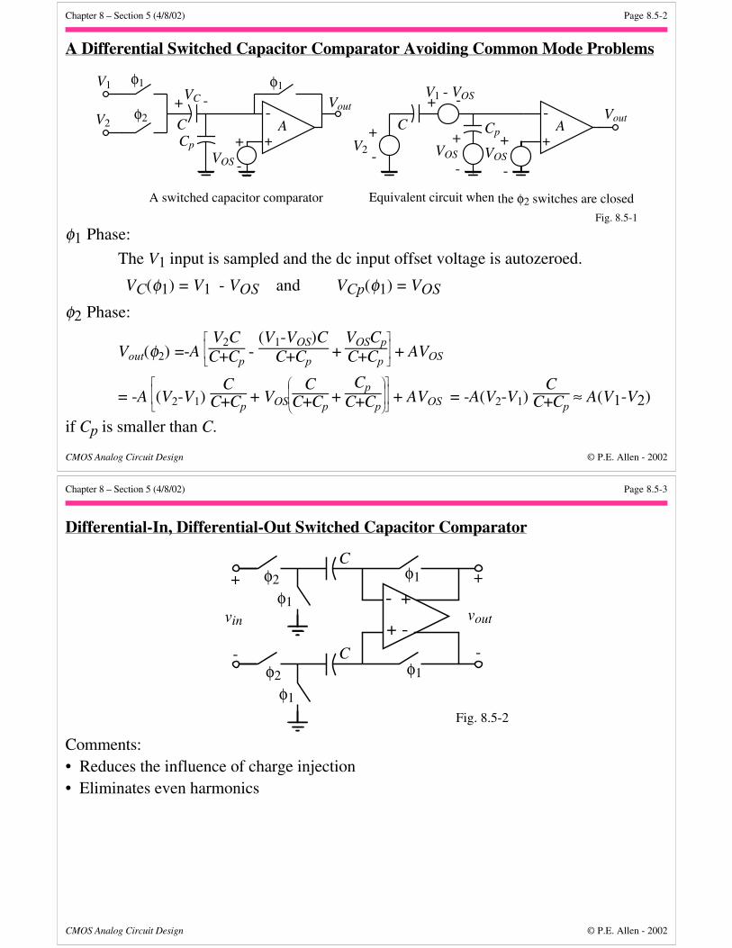
A Differential Switched Capacitor Comparator Avoiding Common Mode Problems
+
-
V1
CCp
φ1
V2
φ1
φ2Vout
+
-VOS
A
+ -VC
+
-V1 - VOS
C Cp
V2
Vout
+
-VOS
A
+ -
+
-+
-VOS
Fig. 8.5-1
A switched capacitor comparator Equivalent circuit when the φ2 switches are closed
φ1 Phase:
The V1 input is sampled and the dc input offset voltage is autozeroed.
VC(φ1) = V1 - VOS and VCp(φ1) = VOS
φ2 Phase:
Vout(φ2) =-A
V2C
C+Cp -
(V1-VOS)CC+Cp
+ VOSCpC+Cp
+ AVOS
= -A
(V2-V1) C
C+Cp + VOS
C
C+Cp +
CpC+Cp
+ AVOS = -A(V2-V1) C
C+Cp ≈ A(V1-V2)
if Cp is smaller than C.
Chapter 8 – Section 5 (4/8/02) Page 8.5-3
CMOS Analog Circuit Design © P.E. Allen - 2002
Differential-In, Differential-Out Switched Capacitor Comparator
-
+
vin +
- +
-
-
+
vout
φ2 φ1
φ1
φ2 φ1
φ1
C
C
Fig. 8.5-2
Comments:• Reduces the influence of charge injection• Eliminates even harmonics
Chapter 8 – Section 5 (4/8/02) Page 8.5-4
CMOS Analog Circuit Design © P.E. Allen - 2002
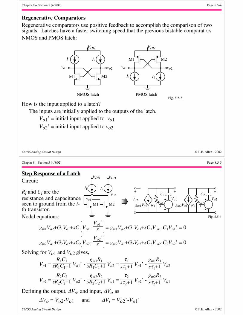
Regenerative ComparatorsRegenerative comparators use positive feedback to accomplish the comparison of twosignals. Latches have a faster switching speed that the previous bistable comparators.NMOS and PMOS latch:
I1 I2
M1 M2
VDD
vo1 vo2
I1 I2
VDD
vo1 vo2
M1 M2
Fig. 8.5-3PMOS latchNMOS latch
How is the input applied to a latch?The inputs are initially applied to the outputs of the latch.
Vo1’ = initial input applied to vo1Vo2’ = initial input applied to vo2
Chapter 8 – Section 5 (4/8/02) Page 8.5-5
CMOS Analog Circuit Design © P.E. Allen - 2002
Step Response of a LatchCircuit:
Ri and Ci are theresistance and capacitanceseen to ground from the i-th transistor.Nodal equations:
gm1Vo2+G1Vo1+sC1
Vo1- Vo1’
s = gm1Vo2+G1Vo1+sC1V o1-C1Vo1’ = 0
gm2Vo1+G2Vo2+sC2
Vo2- Vo2’
s = gm2Vo1+G2Vo2+sC2V o2-C2Vo2’ = 0
Solving for Vo1 and Vo2 gives,
Vo1 = R1C1
sR1C1+1 Vo1’ - gm1R1
sR1C1+1 Vo2 = τ1
sτ1+1 Vo1’ - gm1R1
sτ1+1 Vo2
Vo2 = R2C2
sR2C2+1 Vo2’ - gm2R2
sR2C2+1 Vo1 = τ2
sτ2+1 Vo2’ - gm2R2
sτ2+1 Vo1
Defining the output, ∆Vo, and input, ∆Vi, as
∆Vo = Vo2-Vo1 and ∆Vi = Vo2’-Vo1’
M2M1
I1 I2
vo2
VDD VDD
vo1
gm1Vo2 R1Vo1's
C1Vo1Vo2
+
-
+
-gm2Vo1 R2
Vo2's
C2Vo2
+
-
Fig. 8.5-4
Chapter 8 – Section 5 (4/8/02) Page 8.5-6
CMOS Analog Circuit Design © P.E. Allen - 2002
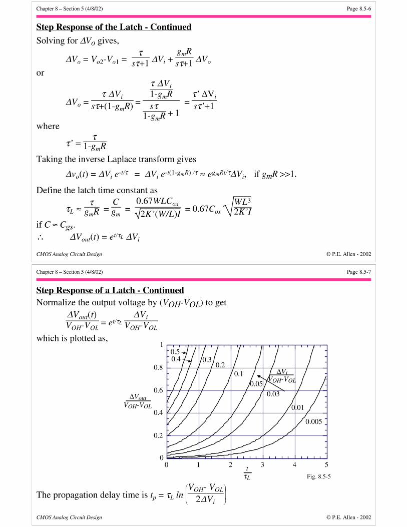
Step Response of the Latch - Continued
Solving for ∆Vo gives,
∆Vo = Vo2-Vo1 = τ
sτ+1 ∆Vi + gmRsτ+1 ∆Vo
or
∆Vo = τ ∆Vi
sτ+(1-gmR) =
τ ∆Vi1-gmRsτ
1-gmR + 1 =
τ’ ∆Vi
sτ’+1
where
τ’ = τ
1-gmR
Taking the inverse Laplace transform gives
∆vo(t) = ∆Vi e-t/τ = ∆Vi e-t(1-gmR) /τ ≈ egmRt/τ∆Vi, if gmR >>1.
Define the latch time constant as
τL ≈ τ
gmR = Cgm
= 0.67WLCox
2K’(W/L)I = 0.67Cox WL3
2K’I
if C ≈ Cgs.∴ ∆Vout(t) = et/τL ∆Vi
Chapter 8 – Section 5 (4/8/02) Page 8.5-7
CMOS Analog Circuit Design © P.E. Allen - 2002
Step Response of a Latch - ContinuedNormalize the output voltage by (VOH-VOL) to get
∆Vout(t)VOH-VOL
= et/τL ∆Vi
VOH-VOL
which is plotted as,
The propagation delay time is tp = τL ln
VOH- VOL
2∆Vi
0
0.2
0.4
0.6
0.8
1
0 1 2 3 4 5tτL
∆VoutVOH-VOL 0.01
0.5 0.4 0.3
0.20.1
0.050.03
0.005
∆Vi
Fig. 8.5-5
VOH-VOL
Chapter 8 – Section 5 (4/8/02) Page 8.5-8
CMOS Analog Circuit Design © P.E. Allen - 2002
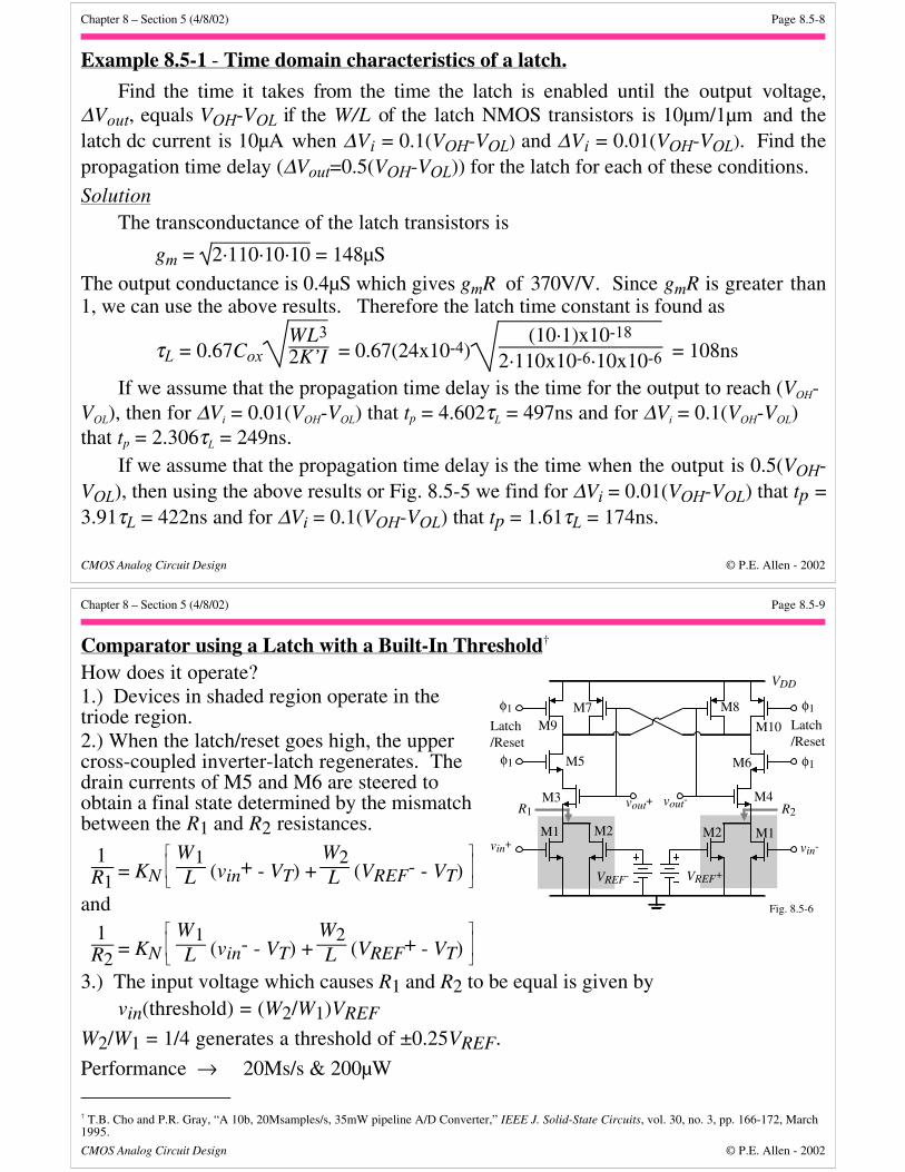
Example 8.5-1 - Time domain characteristics of a latch.
Find the time it takes from the time the latch is enabled until the output voltage,∆Vout, equals VOH-VOL if the W/L of the latch NMOS transistors is 10µm/1µm and thelatch dc current is 10µA when ∆Vi = 0.1(VOH-VOL) and ∆Vi = 0.01(VOH-VOL). Find thepropagation time delay (∆Vout=0.5(VOH-VOL)) for the latch for each of these conditions.
SolutionThe transconductance of the latch transistors is
gm = 2·110·10·10 = 148µS
The output conductance is 0.4µS which gives gmR of 370V/V. Since gmR is greater than1, we can use the above results. Therefore the latch time constant is found as
τL = 0.67CoxWL3
2K’I = 0.67(24x10-4)(10·1)x10-18
2·110x10-6·10x10-6 = 108ns
If we assume that the propagation time delay is the time for the output to reach (VOH-VOL), then for ∆Vi = 0.01(VOH-VOL) that tp = 4.602τL = 497ns and for ∆Vi = 0.1(VOH-VOL)that tp = 2.306τL = 249ns.
If we assume that the propagation time delay is the time when the output is 0.5(VOH-VOL), then using the above results or Fig. 8.5-5 we find for ∆Vi = 0.01(VOH-VOL) that tp =3.91τL = 422ns and for ∆Vi = 0.1(VOH-VOL) that tp = 1.61τL = 174ns.
Chapter 8 – Section 5 (4/8/02) Page 8.5-9
CMOS Analog Circuit Design © P.E. Allen - 2002
Comparator using a Latch with a Built-In Threshold†
How does it operate?1.) Devices in shaded region operate in thetriode region.2.) When the latch/reset goes high, the uppercross-coupled inverter-latch regenerates. Thedrain currents of M5 and M6 are steered toobtain a final state determined by the mismatchbetween the R1 and R2 resistances.
1
R1 = KN
W1L (vin+ - VT) +
W2L (VREF- - VT)
and
1
R2 = KN
W1L (vin- - VT) +
W2L (VREF+ - VT)
3.) The input voltage which causes R1 and R2 to be equal is given byvin(threshold) = (W2/W1)VREF
W2/W1 = 1/4 generates a threshold of ±0.25VREF.
Performance → 20Ms/s & 200µW † T.B. Cho and P.R. Gray, “A 10b, 20Msamples/s, 35mW pipeline A/D Converter,” IEEE J. Solid-State Circuits, vol. 30, no. 3, pp. 166-172, March1995.
VDD
vin+ vin-
vout+ vout-
M1
M3
M5
M7M9
M2
M4
M6
M8
M10
φ1φ1
φ1 φ1
VREF+VREF-
M1M2
Latch/Reset
Latch/Reset
R1 R2
Fig. 8.5-6
Chapter 8 – Section 5 (4/8/02) Page 8.5-10
CMOS Analog Circuit Design © P.E. Allen - 2002
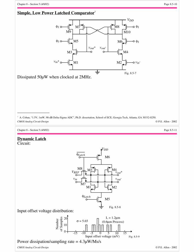
Simple, Low Power Latched Comparator†
VDD
vin+ vin-
vout+ vout-
M1
M3
M5
M7M9
M2
M4
M6
M8
M10
φ1φ1
φ1 φ1
Fig. 8.5-7
Dissipated 50µW when clocked at 2MHz.
† A. Coban, “1.5V, 1mW, 98-dB Delta-Sigma ADC”, Ph.D. dissertation, School of ECE, Georgia Tech, Atlanta, GA 30332-0250.
Chapter 8 – Section 5 (4/8/02) Page 8.5-11
CMOS Analog Circuit Design © P.E. Allen - 2002
Dynamic LatchCircuit:
vout+
VDD
φLatch
φLatch
VREF
vout-vin
M1 M2
M3 M4
M5
M6
M7
M8
Fig. 8.5-8
Input offset voltage distribution:
0 5 10 15-5-10-150
10
20
����������������������N
umbe
rof
Sam
ples
Input offset voltage (mV)
L = 1.2µm(0.6µm Process)σ = 5.65
Fig. 8.5-9
Power dissipation/sampling rate = 4.3µW/Ms/s
Chapter 8 – Section 5 (4/8/02) Page 8.5-12
CMOS Analog Circuit Design © P.E. Allen - 2002
SUMMARY• Discrete-time comparators must work with clocks• Switched capacitor comparators use op amps to transfer charge and autozero• Regenerative comparators (latches) use positive feedback• The propagation delay of the regenerative comparator is slow at the beginning and
speeds up rapidly as time increases• The highest speed comparators will use a combination of open-loop comparators and
latches
Chapter 8 – Section 6 (4/8/02) Page 8.6-1
CMOS Analog Circuit Design © P.E. Allen - 2002
SECTION 8.6 – HIGH-SPEED COMPARATORSObjectiveThe objective of this presentation is:1.) Show how to achieve high-speed comparatorsOutline• Concepts of high-speed comparators• Amplifier-latch comparators• Summary
Chapter 8 – Section 6 (4/8/02) Page 8.6-2
CMOS Analog Circuit Design © P.E. Allen - 2002
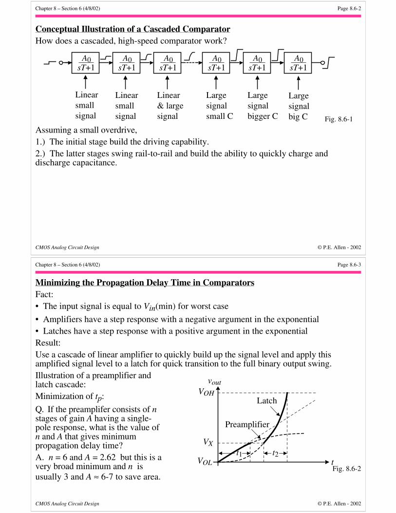
Conceptual Illustration of a Cascaded ComparatorHow does a cascaded, high-speed comparator work?
A0sT+1
A0sT+1
A0sT+1
A0sT+1
A0sT+1
A0sT+1
Linearsmallsignal
Linearsmallsignal
Linear& largesignal
Largesignalsmall C
Largesignalbigger C
Largesignalbig C Fig. 8.6-1
Assuming a small overdrive,1.) The initial stage build the driving capability.2.) The latter stages swing rail-to-rail and build the ability to quickly charge anddischarge capacitance.
Chapter 8 – Section 6 (4/8/02) Page 8.6-3
CMOS Analog Circuit Design © P.E. Allen - 2002
Minimizing the Propagation Delay Time in ComparatorsFact:• The input signal is equal to Vin(min) for worst case
• Amplifiers have a step response with a negative argument in the exponential• Latches have a step response with a positive argument in the exponentialResult:Use a cascade of linear amplifier to quickly build up the signal level and apply thisamplified signal level to a latch for quick transition to the full binary output swing.Illustration of a preamplifier andlatch cascade:Minimization of tp:
Q. If the preamplifer consists of nstages of gain A having a single-pole response, what is the value ofn and A that gives minimumpropagation delay time?A. n = 6 and A = 2.62 but this is avery broad minimum and n isusually 3 and A ≈ 6-7 to save area.
t1
VXt2
voutVOH
VOL t
Latch
Preamplifier
Fig. 8.6-2

Chapter 8 – Section 6 (4/8/02) Page 8.6-4
CMOS Analog Circuit Design © P.E. Allen - 2002
Fully Differential, Three-Stage Amplifier and Latch ComparatorCircuit:
+
- +
-
FB
FB
Reset
Cv1
Cv2
+
- +
-
FB
FB
Reset
Cv3
Cv4
+
- +
-
FB
FB
Reset
Cv5
Cv6
Latch
Reset
Reset
C1
C2
vout
+
-
Clock
+vin - Fig. 8.6-3
Comments:• Autozero and reset phase followed by comparison phase• More switches are needed to accomplish the reset and autozero of all preamplifierssimultaneously• Can run as high as 100Msps
Chapter 8 – Section 6 (4/8/02) Page 8.6-5
CMOS Analog Circuit Design © P.E. Allen - 2002
Preamplifier and Latch CircuitsGain:
Av = - gm1gm3 = -
gm2gm4 = -
KN’(W1/L1)Kp’(W3/L3)
Dominant Pole:
|pdominant| = gm3C =
gm4C
where C is the capacitance seen from theoutput nodes to ground.
If (W1/L1)/(W3/L3) = 100 and thebias current is 100µA, then A = -3.85and the bandwidth is 15.9MHz if C =0.5pF.Comments:• If a buffer is used to reduce the output
capacitance, one must take into account the loss of the buffer.• The use of a preamplifier before the latch reduces the latch offset by the gain of the
preamplifier so that the offset is due to the preamplifier only.
VDD
VBias
FB
FB
Reset
LatchEnable
M1
M2
M3 M4
M5 M6
Q
Q
Preamplifier Latch
Fig. 8.6-4
Chapter 8 – Section 6 (4/8/02) Page 8.6-6
CMOS Analog Circuit Design © P.E. Allen - 2002
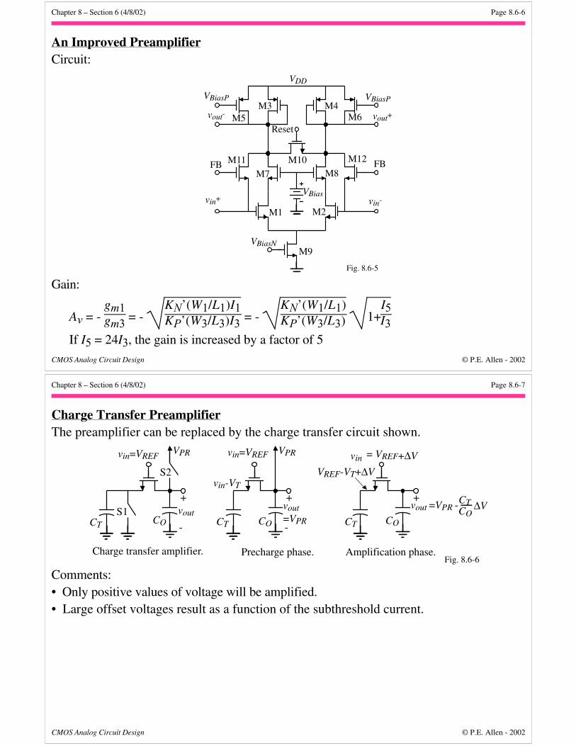
An Improved PreamplifierCircuit:
VDD
M1 M2
M3 M4M5 M6
M7 M8M10
M9
M11 M12
VBiasN
VBias
VBiasP VBiasP
vout+vout-
vin+ vin-
FB FB
Reset
Fig. 8.6-5
Gain:
Av = - gm1gm3 = -
KN’(W1/L1)I1KP’(W3/L3)I3 = -
KN’(W1/L1)KP’(W3/L3) 1+
I5I3
If I5 = 24I3, the gain is increased by a factor of 5
Chapter 8 – Section 6 (4/8/02) Page 8.6-7
CMOS Analog Circuit Design © P.E. Allen - 2002
Charge Transfer PreamplifierThe preamplifier can be replaced by the charge transfer circuit shown.
vin=VREFVPR
S2
S1CT CO
vout
+
-
VPR
CT CO
vout
=VPR
+
-
vin-VT
vin = VREF+∆V
CT CO
vout =VPR -+
VREF-VT+∆V
CTCO
∆V
Charge transfer amplifier. Precharge phase. Amplification phase.Fig. 8.6-6
vin=VREF
Comments:• Only positive values of voltage will be amplified.• Large offset voltages result as a function of the subthreshold current.
Chapter 8 – Section 6 (4/8/02) Page 8.6-8
CMOS Analog Circuit Design © P.E. Allen - 2002
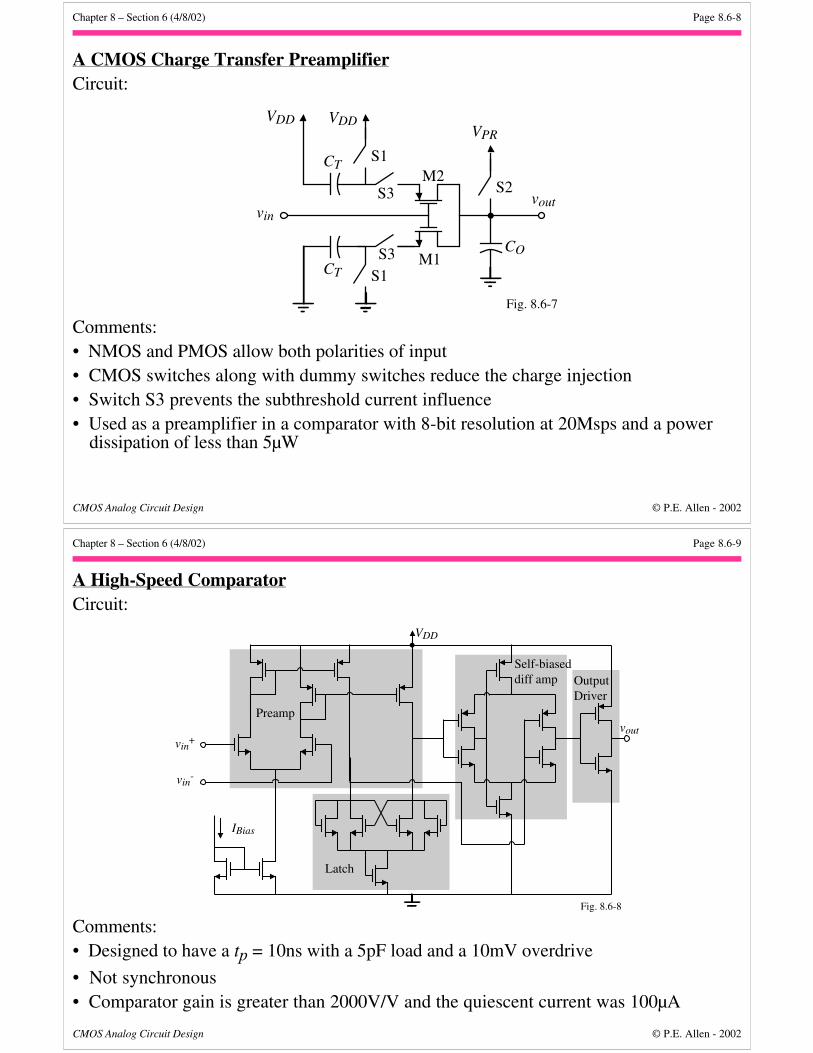
A CMOS Charge Transfer PreamplifierCircuit:
vin
VDD VDDVPR
CT
CTM1
M2S1
S2
CO
vout
S1
S3
S3
Fig. 8.6-7
Comments:• NMOS and PMOS allow both polarities of input• CMOS switches along with dummy switches reduce the charge injection• Switch S3 prevents the subthreshold current influence• Used as a preamplifier in a comparator with 8-bit resolution at 20Msps and a power
dissipation of less than 5µW
Chapter 8 – Section 6 (4/8/02) Page 8.6-9
CMOS Analog Circuit Design © P.E. Allen - 2002
A High-Speed ComparatorCircuit:
IBias
Preamp
Latch
Self-biaseddiff amp Output
Driver
voutvin
+
vin-
VDD
Fig. 8.6-8
Comments:• Designed to have a tp = 10ns with a 5pF load and a 10mV overdrive
• Not synchronous• Comparator gain is greater than 2000V/V and the quiescent current was 100µA
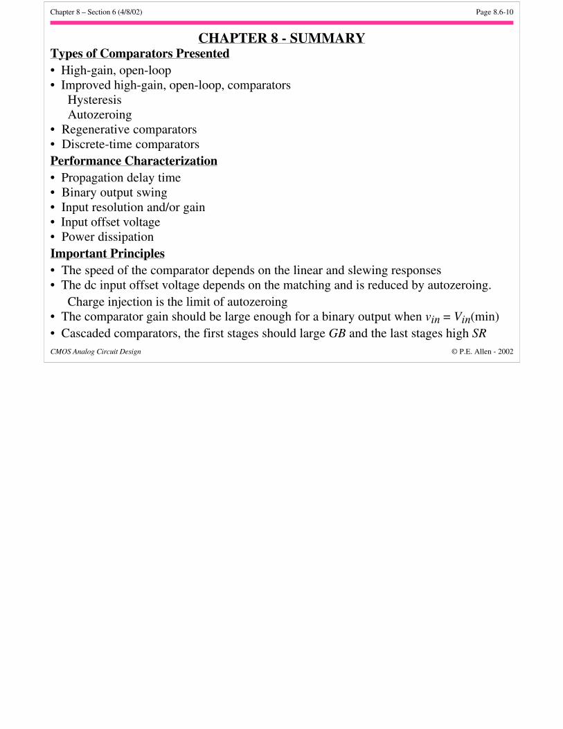
Chapter 8 – Section 6 (4/8/02) Page 8.6-10
CMOS Analog Circuit Design © P.E. Allen - 2002
CHAPTER 8 - SUMMARYTypes of Comparators Presented• High-gain, open-loop• Improved high-gain, open-loop, comparators
HysteresisAutozeroing
• Regenerative comparators• Discrete-time comparatorsPerformance Characterization• Propagation delay time• Binary output swing• Input resolution and/or gain• Input offset voltage• Power dissipationImportant Principles• The speed of the comparator depends on the linear and slewing responses• The dc input offset voltage depends on the matching and is reduced by autozeroing.
Charge injection is the limit of autozeroing• The comparator gain should be large enough for a binary output when vin = Vin(min)• Cascaded comparators, the first stages should large GB and the last stages high SR