Secondary Electron Yield Measurements of TiN Coating and TiZrV
15
Linear Collider Collaboration Tech Notes LCC-0128 SLAC-TN-03-052 October 2003 Secondary Electron Yield Measurements of TiN Coating and TiZrV Getter Film F. Le Pimpec, F. King, R.E. Kirby, M. Pivi Stanford Linear Accelerator Center Stanford University 2575 Sand Hill Road Menlo Park, CA Abstract: In the beam pipe of the positron Main Damping Ring (MDR) of the Next Linear Collider (NLC), ionization of residual gases and secondary electron emission give rise to an electron cloud which can cause the loss of the circulating beam. One path to avoid the electron cloud is to ensure that the vacuum wall has low secondary emission yield and, therefore, we need to know the secondary emission yield (SEY) for candidate wall coatings. We report on SEY measurements at SLAC on titanium nitride (TiN) and titanium-zirconium-vanadium (TiZrV) thin sputter-deposited films, as well as describe our experimental setup.
Transcript of Secondary Electron Yield Measurements of TiN Coating and TiZrV

LCC-0128 SLAC-TN-03-052 October 2003
Abstract: In the beam residual gases and sebeam. One path to avtherefore, we need tomeasurements at SLAas well as describe ou
Linear Collider Collaboration Tech Notes
Secondary Electron Yield Measurements of TiN Coating and TiZrV Getter Film
F. Le Pimpec, F. King, R.E. Kirby, M. Pivi
Stanford Linear Accelerator Center Stanford University
2575 Sand Hill Road Menlo Park, CA
pipe of the positron Main Damping Ring (MDR) of the Next Linear Collider (NLC), ionization of condary electron emission give rise to an electron cloud which can cause the loss of the circulating oid the electron cloud is to ensure that the vacuum wall has low secondary emission yield and, know the secondary emission yield (SEY) for candidate wall coatings. We report on SEY C on titanium nitride (TiN) and titanium-zirconium-vanadium (TiZrV) thin sputter-deposited films, r experimental setup.

SLAC-TN-03-052 1
Secondary Electron Yield Measurements of TiNCoating and TiZrV Getter Film
F. Le Pimpec, F. King, R.E. Kirby, M. PiviSLAC, 2575 Sand Hill Road, Menlo Park, CA 94025
9th October 2003
Abstract
In the beam pipe of the positron Main Damping Ring (MDR) of the Next LinearCollider (NLC), ionization of residual gases and secondary electron emission giverise to an electron cloud which can cause the loss of the circulating beam. One pathto avoid the electron cloud is to ensure that the vacuum wall has low secondary emis-sion yield and, therefore, we need to know the secondary emission yield (SEY) forcandidate wall coatings. We report on SEY measurements at SLAC on titanium ni-tride (TiN) and titanium-zirconium-vanadium (TiZrV) thin sputter-deposited films,as well as describe our experimental setup.
1 Introduction
Beam-induced multipacting, which is driven by the electric field of successive positivelycharged bunches, arises from a resonant motion of electrons that were initially generatedor by gas ionization or by secondary emission from the vacuum wall. These electronsthen bounce back and forth between opposite walls of the vacuum chamber. The electroncloud density depends on characteristics of the positively charged circulating beam (bunchlength, charge and spacing) and the secondary electron yield and spectrum of the wallsurface from which the starting electrons arise. The electron cloud effect (ECE), dueto multipacting, has been observed or is expected at many storage rings [1]. The spacecharge of the cloud, if sufficient, can lead to a loss of the beam or, at least, to a drasticreduction in bunch luminosity.
In order to minimize the electron cloud problem which might arise in the NLC, weare looking to a solution involving surface coating of the secondary electron emittingvacuum wall. The SEY of technical surfaces has been measured in the past at SLAC [2][3], at CERN Fig.1 [4] [5] and in other labs [6]. In this paper we present measurementsof the SEY of materials previously measured and known to have low SEY [7] [8] [9] liketitanium-nitride thin film (TiN) and titanium-zirconium-vanadium getter film (TiZrV).

� � �
�
� � �
�
� � �
�
� � � � � � � � � � � � � � � � � � � � � � � � � � � � � � � � � � �
� � � � � � � � � � � � � � � � � � � �
��� �������� ���������������� ������� �����
� � � � � � � � �
� � � � � � �
� � � � �
� � � � � � � � � �
� � � � � � � � � � � � �
� � � � � � � � � � � � � � � � !
� � � � � � " # � � � � � � � $ � � % � & � $ ' !
Figure 1: SEY of baked technical surfaces. 300◦C for 24hr [10]
2 Experiment Description
The system used to measure SEY is composed of two coupled stainless steel (S/S) UHVchambers where the pressure is in the low 10−10 Torr scale in the measurement chamberand high 10−9 Torr scale in the ”load lock” chamber, Fig.2. Samples individually screwedto a carrier plate, are loaded first onto an aluminium transfer plate in the load lockchamber, evacuated to a low 10−8 Torr scale, and then transferred to the measurementchamber.
The measurement chamber has two electron guns and a soft (1.49 keV) x-ray source.One electron gun (energy, 1-20 keV) is used for Auger electron spectroscopy (AES) lightelement surface contamination analysis. The x-ray source is used to excite photoelectronsfor surface chemical valence analysis, called ESCA (Electron Spectroscopy for ChemicalAnalysis). TiN stoichiometry is measured by ESCA technique which is also called XPS(X-ray Photoelectron Spectroscopy).
The principle of XPS is to collect photoelectrons ejected by x-rays of known energynear the surface (1 - 5 nm information depth). The emitted electrons have an energy Ek
which is given by equation 1
Ek = hν − Eb − Φ (1)
where hν is the energy of the incident photon, Eb the binding energy of the electronrelative to the Fermi level of the material and Φ the spectrometer work function. Thespectrum of the measured kinetic energy gives the spectrum of the binding energy of thephotoelectrons.
The x-ray source is also used for exciting secondary X-ray Fluorescence (XRF) forthickness measurement of the deposited TiN overlayers. The second electron gun (0-3 keV) is used measure the SEY, and can also be used to electron condition the surface.
2

An ion gun is available for cleaning the samples by sputtering and for ion conditioningsurfaces.
Figure 2: Experimental system used for surface analysis
After all samples (up to ten or so) are transferred into the measurement chamber,one sample at a time is loaded, on its individual carrier plate, onto a manipulator arm
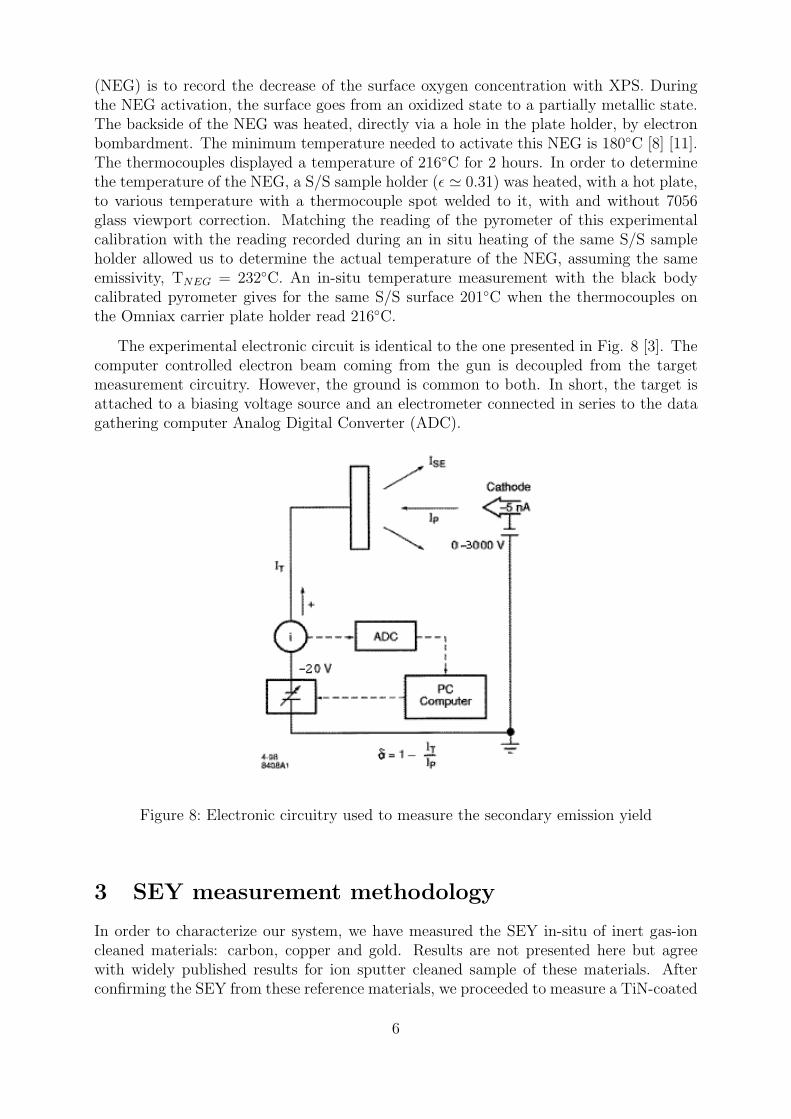
(Vacuum Generators ”Omniax”). The Omniax� carrier plate holder design is shown inFig.4. Two thermocouples are installed on this holder plate as well as heating filament andsample connection wires. Samples can be heated via a tungsten wire filament, Fig.3, byradiation or by electron bombardment. Electron bombardment is achieved by biasing thefilament negatively. The Omniax sample holder is insulated from ground via an aluminaceramic and by several thermal shield plates insulated via four sapphire balls, Fig.3 andFig.4.
The sample carrier plates are made of molybdenum (for attaining the highest tem-peratures) or stainless steel, Fig.5. This plate will support one sample which is held bycorner screws onto its surface. This design allows the plate to then slide into the railsof the Omniax plate holder, cf Fig.3. An example of an aluminium prototype carrierplate is shown in Fig.6 and Fig.7. Note that on Fig.6 the holes for the screws are notdrilled. In this configuration, the thermocouples are not attached directly to the carrierplate but indirectly through the holder plate. Sample temperatures are compared to thethermocouple temperatures by using a black body-calibrated infrared pyrometer (0.8 µm- 1.3 µm bandpass) which is corrected for absorption by the 7056 glass viewport of themeasurement chamber and the sample emissivity (ε) of 0.2 - 0.4.
A good way to monitor the activation process of the TiZrV non-evaporable getter
3
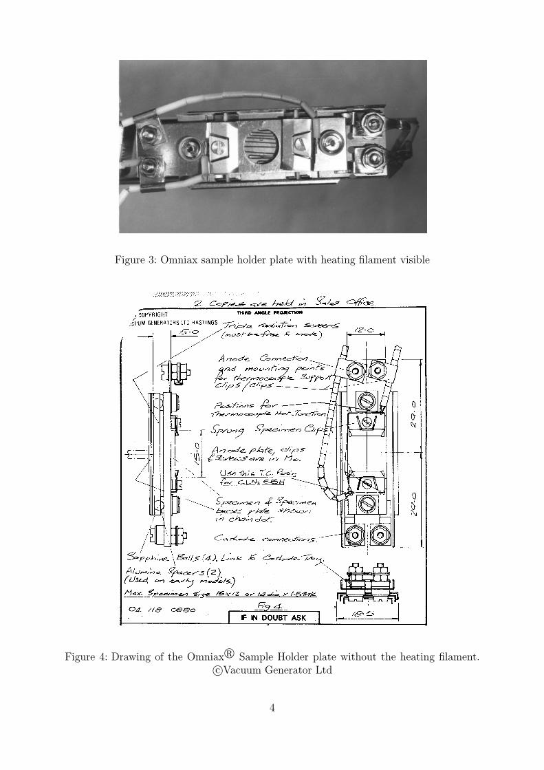
Figure 3: Omniax sample holder plate with heating filament visible
Figure 4: Drawing of the Omniax� Sample Holder plate without the heating filament.c©Vacuum Generator Ltd
4

Figure 5: Sketch of the Sample carrier plate made in stainless steel. Dimensions are ininches
Figure 6: Sample holder proto-type in aluminium. The blackdots are the location of the screw
sample mounting holes
Figure 7: Bottom side of the sam-ple holder
5
(NEG) is to record the decrease of the surface oxygen concentration with XPS. Duringthe NEG activation, the surface goes from an oxidized state to a partially metallic state.The backside of the NEG was heated, directly via a hole in the plate holder, by electronbombardment. The minimum temperature needed to activate this NEG is 180◦C [8] [11].The thermocouples displayed a temperature of 216◦C for 2 hours. In order to determinethe temperature of the NEG, a S/S sample holder (ε � 0.31) was heated, with a hot plate,to various temperature with a thermocouple spot welded to it, with and without 7056glass viewport correction. Matching the reading of the pyrometer of this experimentalcalibration with the reading recorded during an in situ heating of the same S/S sampleholder allowed us to determine the actual temperature of the NEG, assuming the sameemissivity, TNEG = 232◦C. An in-situ temperature measurement with the black bodycalibrated pyrometer gives for the same S/S surface 201◦C when the thermocouples onthe Omniax carrier plate holder read 216◦C.
The experimental electronic circuit is identical to the one presented in Fig. 8 [3]. Thecomputer controlled electron beam coming from the gun is decoupled from the targetmeasurement circuitry. However, the ground is common to both. In short, the target isattached to a biasing voltage source and an electrometer connected in series to the datagathering computer Analog Digital Converter (ADC).
Figure 8: Electronic circuitry used to measure the secondary emission yield
3 SEY measurement methodology
In order to characterize our system, we have measured the SEY in-situ of inert gas-ioncleaned materials: carbon, copper and gold. Results are not presented here but agreewith widely published results for ion sputter cleaned sample of these materials. Afterconfirming the SEY from these reference materials, we proceeded to measure a TiN-coated
6
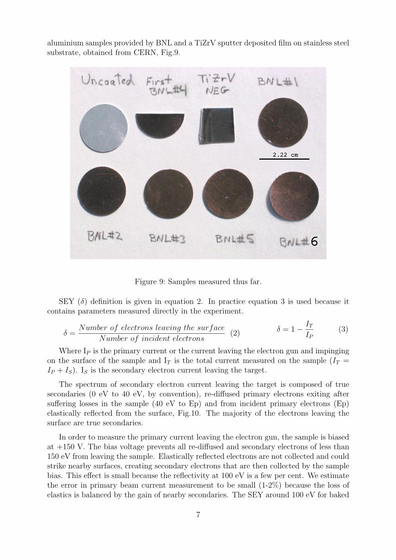
aluminium samples provided by BNL and a TiZrV sputter deposited film on stainless steelsubstrate, obtained from CERN, Fig.9.
Figure 9: Samples measured thus far.
SEY (δ) definition is given in equation 2. In practice equation 3 is used because itcontains parameters measured directly in the experiment.
δ =Number of electrons leaving the surface
Number of incident electrons(2) δ = 1− IT
IP
(3)
Where IP is the primary current or the current leaving the electron gun and impingingon the surface of the sample and IT is the total current measured on the sample (IT =IP + IS). IS is the secondary electron current leaving the target.
The spectrum of secondary electron current leaving the target is composed of truesecondaries (0 eV to 40 eV, by convention), re-diffused primary electrons exiting aftersuffering losses in the sample (40 eV to Ep) and from incident primary electrons (Ep)elastically reflected from the surface, Fig.10. The majority of the electrons leaving thesurface are true secondaries.
In order to measure the primary current leaving the electron gun, the sample is biasedat +150 V. The bias voltage prevents all re-diffused and secondary electrons of less than150 eV from leaving the sample. Elastically reflected electrons are not collected and couldstrike nearby surfaces, creating secondary electrons that are then collected by the samplebias. This effect is small because the reflectivity at 100 eV is a few per cent. We estimatethe error in primary beam current measurement to be small (1-2%) because the loss ofelastics is balanced by the gain of nearby secondaries. The SEY around 100 eV for baked
7

stainless steel is close to 1.1, Fig.1. With regard to the gun current as a function ofenergy, it starts at zero for zero energy and smoothly increased to its saturation value at70 eV. We measure the magnitude and functional dependence of the beam current up tosomewhat higher value(100 eV) and use a constructed lookup table of the beam currentfor SEY calculations. Not biasing the sample with a high enough voltage will lead toan underestimation of the beam current. This is easily understood from the secondaryspectrum, Fig.10. The selected 2 nA gun current is measured for a gun energy of 0-100 eVby energy steps of 10 eV (0-3000 eV range) or 2 eV (0-300 eV range).
Actual measurement of the SEY is done by biasing the sample to -20 V. This retardingfield repels most secondaries from adjacent parts of the system that are excited by theelastically reflected primary beam. SEY measurements are done twice, once between 0 eVto 3000 eV with 10 eV steps, then between 0 eV to 300 eV, with 2 eV steps. The finalenergy of the primary electrons is respectively 2980 eV and 280 eV because of the bias.The primary beam current function is measured and recorded each time before an SEYmeasurement, and with the same step in energy for the electron beam. A fresh currentlookup table is created with each measurement.The purpose of the second measurement, 0 eV to 300 eV, is to try to understand thestructure of the SEY curve at very low energy. Several points are important, though.
1. Because of the negative sample bias, primary electrons near 0 eV at the sample areassured to be leaving the gun (20 eV departure) and arriving at (20 eV -20 V) eV.
2. Because of the algorithm used to calculate the SEY from the primary and samplecurrents at 0 eV incident energy, a divide by 0 blowup occurs. To avoid this problem,the first point at 0 eV is forced to value one. The first ”true” data point is at 2 eVfor 300 eV range and 10 eV for 3000 eV range.
3. The uncertainty in the sample electrometer current reading is set by the inputoperational amplifier bias leakage, ± 20 pA.
4. Using sample current to determine SEY excludes the elastically reflected electronsfrom the calculation (they would need to be collected by an external to the samplegrid structure). That serves to increase the SEY (less sample current) by 1-3%.This is fortuitously balanced by the fact that the -20 V bias does not repel 100% ofnearby surface secondaries.
The consequence of all of these points is that the SEY measurements are just that,”secondary”. Which means that it does not include the elastics. The SEY measurementsare however, accurate. It is important to not look at the SEY at low primary energyand try to conclude something about elastic reflectivity. Data below 20 eV comes froma band structure and are a combination of diffraction from the crystalline structure andenergy absorption by the material [12]. Surface effects such as roughness can also changethe SEY.
8

Figure 10: Spectrum of a sec-ondary electron beam from a300 eV incident primary beamimpinging on a TiN on Al sub-
strate sample [13]
Figure 11: TiN thickness mea-sured by x-ray fluorescence of theTi K-line of four BNL samples
4 Results and Comments
The TiN coating, made at Brookhaven National Laboratory (BNL), was deposited ontoaluminium alloy substrates, following the same recipe described in [9]. For the SpallationNeutron Source (SNS) project, the coating was done on S/S. According to BNL, theexpected film thickness is around 1000 A. We measured the actual sample thicknessesusing XRF, Fig.11.
The principle of XRF is to collect secondary x-rays generated and exiting the samplewhen bombarded by primary incident x-rays. The secondary fluorescence yield is highestsomewhat above the K-absorption edge of Ti, so primary x-rays of 7 keV are used forthe excitation of the Ti-Kα line (4.51 keV). A TiN film of similar known thickness (byRutherford backscatter spectrometry, performed at an outside lab) is used to calibratethe technique.The height of the measured Ti-Kα line, using a Si Li-drifted x-ray detector, is linearlyproportional to the number of Ti atoms in the film. Results are shown for a few samplesin Fig.11.
SEY measurements results of six different ”as received” TiN samples are displayed inFig.12 and Fig.13. The electron beam impinging onto the surface is of the order of 2 nAover an area of less than a mm2. Typically the beam size is between 0.2 mm to 0.4 mmin diameter. The low current is necessary in order to avoid surface conditioning duringSEY measurement. The size of the beam can be checked by using a fluorescent screen, oris inferred from secondary electron microscopical imaging (available on the measurementsystem and used to precisely choose the point of SEY measurement).
The SEY of the samples varies from 1.5 to 2.5, with the thickest film samples displayingthe lower SEY. However, we have no data concerning the roughness, and the roughnesscan be a factor which can change the SEY. The commonly accepted hypothesis is that,for a given chemical surface, the rougher surface has a lower SEY than a smoother one[4]. The irregularity in the SEY, at near maximum, for sample TiN#4 and TiN#6 canbe due to a non uniform spot emitting secondaries with two different yields. The result
9
0 250 500 750 1000 1250 1500 1750 2000 2250 2500 2750 30000.4
0.6
0.8
1
1.2
1.4
1.6
1.8
2
2.2
2.4
Energy : eV
Sec
onda
ry E
lect
ron
Yie
ld
Secondary Electron Yield of TiN As Received (BNL/SNS sample)
TiN #1TiN #2TiN #3TiN #4TiN #5TiN #6
Figure 12: SEY of different TiNsample for electron energy be-
tween 0-2980 eV
0 25 50 75 100 125 150 175 200 225 250 275 3000.4
0.6
0.8
1
1.2
1.4
1.6
1.8
2
2.2
2.4
Energy : eV
Sec
onda
ry E
lect
ron
Yie
ld
Secondary Electron Yield of TiN As Received (BNL/SNS sample)
TiN #1TiN #2TiN #3TiN #4TiN #5
Figure 13: SEY of different TiNsample for electron energy be-
tween 0-280 eV.
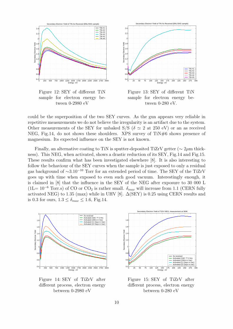
could be the superposition of the two SEY curves. As the gun appears very reliable inrepetitive measurements we do not believe the irregularity is an artifact due to the system.Other measurements of the SEY for unbaked S/S (δ � 2 at 250 eV) or an as receivedNEG, Fig.14, do not shows these shoulders. XPS survey of TiN#6 shows presence ofmagnesium. Its expected influence on the SEY is not known.
Finally, an alternative coating to TiN is sputter-deposited TiZrV getter (∼ 2µm thick-ness). This NEG, when activated, shows a drastic reduction of its SEY, Fig.14 and Fig.15.These results confirm what has been investigated elsewhere [8]. It is also interesting tofollow the behaviour of the SEY curves when the sample is just exposed to only a residualgas background of ∼3.10−10 Torr for an extended period of time. The SEY of the TiZrVgoes up with time when exposed to even such good vacuum. Interestingly enough, itis claimed in [8] that the influence in the SEY of the NEG after exposure to 30 000 L(1L= 10−6 Torr.s) of CO or CO2 is rather small. δmax will increase from 1.1 (CERN fullyactivated NEG) to 1.35 (max) while in UHV [8]. ∆(SEY) is 0.25 using CERN results andis 0.3 for ours, 1.3 ≤ δmax ≤ 1.6, Fig.14.
0 250 500 750 1000 1250 1500 1750 2000 2250 2500 2750 30000.4
0.6
0.8
1
1.2
1.4
1.6
1.8
2
Energy : eV
Sec
onda
ry E
lect
ron
Yie
ld
As receivedActivated 216C ?? 2 HrsActivated (16hrs in Vac)Activated (11 Days in Vac)Activated (22 Days in Vac)
Figure 14: SEY of TiZrV afterdifferent process, electron energy
between 0-2980 eV
0 25 50 75 100 125 150 175 200 225 250 275 3000.4
0.6
0.8
1
1.2
1.4
1.6
1.8
Energy : eV
Sec
onda
ry E
lect
ron
Yie
ld
Secondary Electron Yield of TiZrV NEG, measurement at 300K
As receivedActivated 216C ?? 2 HrsActivated (16hrs in Vac)Activated (11 Days in Vac)Activated (22 Days in Vac)
Figure 15: SEY of TiZrV afterdifferent process, electron energy
between 0-280 eV
10

If we consider, at first, that our SEY measurement is errorless, one can argue thatour activation was not complete. Hence, some initial air formed oxide is still present andthe surface chemistry is not identical to a fully activated NEG, hence explaining our δafter activation of 1.3. In this case the SEY should still not increase above 1.35 [8] as thegetter does not have many pumping sites left. However, this hypothesis might have to bediscarded as the minimal temperature we are certain to have achieved is at least 201◦C.As a result of a power outage of an hour, during the eleven days of monitoring, an iongauge, a residual gas analyser and the ion pump were turned off. At the switch onof the gauges, hot filaments release gases in the system before being pumped away bythe ion pump. The recorded pressure in the system was at the switch on of the gauges∼6.10−10 Torr. This kind of incident also can happen in an accelerator, and it is interestingto see that this effect leads to the recontamination of the getter. Between the days elevenand days twenty, the system was used to XPS other samples. Due to the transfer ofsamples from the load lock chamber to the measurement chamber, the pressure rose upmomentarily to ∼2.10−9 Torr.If CO or CO2 exposure do not seem to affect the increase of δ, air exposure does [8]. Itis possible that opening our baked measurement chamber (P ∼ 3.10−10 Torr) to the loadlock chamber (P ∼ 9.10−9 Torr), which is frequently open to air, can be consider as anair exposure. Hence, there is no contradiction between CERN [8] and our results.
XPS analysis was carried out to observe the evolution of the carbon chemistry duringthis 20 days and compared to the XPS spectrum taken after the end of the activation.The XPS spectrum shows a slight rise of the oxygen peak and a double valency carbon1s peak. The elemental carbon peak has an energy of ∼285 eV and the oxidized carbonpeak has an energy of ∼288 eV. The oxidized carbon peak after the end of the activationat 288 eV was barely present, Fig.16, blue plot. The NEG is at 180◦C. This result is verysimilar to that of a cleanly-scraped carbon surface, measured at room temperature. Aftersixteen hours of pumping, green plot, the oxidized state of the carbon shows up. Thisstate becomes dominant after eleven days of pumping and keep increasing after 20 days,gray curve. In the last cases the NEG was at room temperature. The plots presented inFig.16 are a fit of the actual data. This increase of the C-O peak implies that the SEYshould also increase, as is usually the case for oxidized metal surfaces.
The roughness (R) of the TiZrV film is unknown. This roughness affects not only theSEY [4] but also the pumping capacity and speed of the NEG. TiZrV deposited on S/Sis relatively smooth (R�1) and is much rougher on an aluminium substrate [11]. Let’sassume that our system was for twenty days at ∼3.10−10 Torr, the CO being presentat 15% of the total spectrum, and that the sticking coefficient σ for CO is 0.4. Thesticking coefficient decreases when the TiZrV NEG has pumped almost half of a monolayer(1 ML ∼1015 molecules-cm−2 for a smooth surface) by a factor 10 after reaching 1 ML,and by a factor 100 after 10 ML [11]. A monolayer of a surface (MLs) can be defined as :MLs = ML × R [10]. The frequency of collision ν (molecules.s−1.cm−2) equation 4 andthe total amount of CO per cm−2 pumped by the NEG in one day is given by equation 5.
ν = 3.5123P√M T
(4) NCO = ν × 86400× σ (5)
where P is the pressure in Torr, M the atomic mass and T is the temperature in K.
After one day of pumping the NEG would have pumped ∼0.6 ML. Assuming thatfor ten days the sticking coefficient is 0.04, the NEG would have pumped an additional∼0.6 ML. According to the rough calculation for the total amount of CO pumped by
11

2792802812822832842852862872882892902912922930
0.25
0.5
0.75
1
1.25
1.5
1.75
2
2.25
Binding Energy : eV
Pho
toel
ectr
on In
tens
ity :a
u
NEG at 180 CNEG 16hrs pumpingNEG 11 days pumpingNEG 20 days pumping
C Peak
C−O Peak
Figure 16: XPS C peak of a TiZrV film after the end of activation
the NEG, the XPS of 11 days and 20 days should be similar, as the NEG is basicallysaturated. This increase of the C-O peak, Fig.16, suggests that the surface still had someremaining pumping speed after eleven days of vacuum exposure.NEG provides a nice solution for a distributed pumping inside a vacuum chamber, whenactivated. Our small sample, a few cm2, being at 300 K pumped all of the residual gas inthe chamber except CH4. In a few meters long NEG coated chamber the contaminationcomes from outgassing surfaces outside this chamber, since the NEG film is a diffusionbarrier for outgassing molecules of the substrate. Depending of the average vacuum inthe machine and the length of the NEG chambers, the recontamination of the surfacemight take longer than for our sample. Hence, the SEY might not increase as rapidly asmeasured here, Fig.14 and Fig.15.
Also, it has to be taken into account that the pumping lifetime of thin film NEGdepends on its thickness and the number of activation cycles [11]. The influence of thethickness of the film should also be taken into account, when calculating the impedancefor the image current on the vacuum chamber wall, due to a passing particle beam. Therequirement on the conductivity and the good mechanical performance after an in-situbake of the substrate is of importance.For the main damping rings, current design will use aluminium-alloy chamber. Aluminiumlooses mechanical strength when heated above 150◦C. An adequate substrate for TiN orTiZrV which fulfills the mechanical requirements is the alloy, Al 6061, or Al 6060 which iseasier to extrude. Their conductivity is ∼1.4 times lower than for pure aluminium. SEYmeasurements on a TiN film deposited on Al 6061 has already been carried out at SLAC[13].
5 Conclusion
We have presented a report on the status of the SEY experiment carried out at SLAC.Description of our experimental system has been presented.
First results on as-received TiN sample and on an as-received TiZrV getter have been
12
shown. In the case of the getter, the influence of the activation and recontaminationby its pumping action were investigated. The maximum SEY δ increased from ∼1.3to ∼1.5 after eleven days and to ∼1.6 after twenty-two days of exposure to a vacuumof ∼3.10−10 Torr. Our SEY results seem to disagree with CERN [8]. First of all, ourstarting δmax is 1.3 compare to 1.1 [8]. Second, we have an increase in δmax above theCERN-predicted 1.35 [8]. This matter should be investigated further as the implicationto electron cloud development is of importance for a positively charged beam running inan accelerator.
Values of δ for energies below 20 eV should be used carefully if plugged into simulation.It is planned to investigate further this part of the SEY curve, as has been done at CERN[14].
Additionally, we will study the influence of various treatments, such as the in-situbakeout of TiN, electron conditioning applied for the NLC case, and also the influence ofion conditioning. By conditioning we mean bombarding the surface with a given spectrumin energy of electrons and ions. Different species of ions can also be investigated.It has to be stressed that conditioning (dose effect) is a very efficient way of lowering theSEY of any technical surfaces to almost the same value (δ = 1.2); and thus independentlyof the initial δ [4]. However, such measurements are time consuming and might not berelevant to the operation of an accelerator, depending on the flux of electrons associatedwith post-commissioning production operation.
6 Acknowledgments
We would like to thank P. He and H.C. Hseuh at BNL for providing the TiN samplesand the EST group from C. Benvenuti at CERN for the TiZrV sample. We also thankA. Wolski at LBNL for shepherding the production of sample plates, and in the nearfuture, for thin film samples coming from LBNL. Most valuable was the work of G.Collet and E. Garwin, SLAC, for converting and baking the XPS system for use on SEYmeasurements.
References
[1] M. Pivi et al. Recent Electron-Cloud Simulation Results for the Main Damping Ringsof the NLC and the TESLA Linear Colliders. In PAC, Portland, Or, USA, 2003.SLAC-PUB-9814.
[2] P. Prieto and R.E. Kirby. X-ray photoelectron spectroscopy study of the difer-ence between reactively evaporated and direct sputter-deposited TiN films and theiroxidation prperties. Journal of Vacuum Science and Technology, A13(6), 1995.
[3] R.E. Kirby F.K. King. Secondary Emission Yield from PEP-II accelerator material.Nuclear Instruments and Methods in Physics Research A, A469, 2001.
[4] N. Hilleret et al. http://clic-structures-working-group.web.cern.ch/clic-structures-working-group/min/2000/18-9-2000/noel.pdf.
13

[5] N. Hilleret et al. The Secondary Electron Yield of Technical Materials and its Vari-ation with Surface Treatments. In EPAC , Vienna, Austria, 2000.
[6] S. Kato, M. Nishiwaki. Study on Electron Emission from Some Metals and CarbonMaterials and the Surface Characterization. In 49th AVS, 2002.
[7] J-M. Laurent, U. Iriso Ariz. Multipactor Tests of a NEG coated Chamber. Technicalreport, CERN-LHC-VAC 03-04, 2003.
[8] C. Scheurlein. The Activation of Non-evaporable Getters Monitored by AES, XPS,SSIMS and Secondary Electron Yield Measurements. Technical report, CERN-THESIS- 2002- 026, 2002.
[9] P. He et al. Development of TiN coating for SNS Ring Vacuum Chambers. In PAC2001, 2001.
[10] F. Le Pimpec. Etude de la Desorption Moleculaire Induite par Transitions Electron-iques dans les Surfaces Techniques. PhD thesis, Universite Pierre et Marie Curie Paris6, 2000. http://documents.cern.ch/archive/ electronic/cern/preprints/thesis/thesis-2000-017.pdf.
[11] C. Benvenuti et al. Vacuum Properties of TiZrV non-evaporable getter films. Vac-uum, 60:57, 2001.
[12] E. Tamura et al. Energy-Dependence of Inner Potential in Fe from Low-EnergyElectron Absorption (Target Current). Technical report, SLAC-PUB-3594, 1985.
[13] R.E. Kirby, F.K. King. Secondary Electron Emission from Accelerator Materials:Transparencies. Technical report, SLAC-PUB-8380, 2000.
[14] R. Cimino, I. Collins. A Surface Science Approach to Study ElectronCloud Phenomena. In Damping Ring Workshop, Daresbury UK, 2003.http://www.astec.ac.uk/conf/dampingring/proceedings.html.
14