Schematic of an Inverter Circuit - Santa Clara University · Select METAL1.PORT (2) on RHS of the...
25
Copyright©2006 Layout and Layout Verification of an Inverter Circuit Santa Clara University Department of Electrical Engineering By Piyush Panwar Under Guidance of Dr Samiha Mourad Date of Last Revision: August 7, 2010
Transcript of Schematic of an Inverter Circuit - Santa Clara University · Select METAL1.PORT (2) on RHS of the...

Copyright©2006
Layout and Layout Verification
of an Inverter Circuit
Santa Clara University
Department of Electrical Engineering
By
Piyush Panwar
Under Guidance of Dr Samiha Mourad
Date of Last Revision: August 7, 2010

Copyright©2006
2
Table of Contents
1. Objective ......................................................................................................................... 3
2. Setup & Preparation ........................................................................................................ 4
3. Launching IC Studio ....................................................................................................... 5
4. Opening the project ......................................................................................................... 6
1. Opening icstudio and opening the project .............................................................. 6
2. Opening Layout Cell ............................................................................................... 6
5 Drawing the Layout ......................................................................................................... 9
1. Actual Inverter Layout .............................................................................................. 10
6. Adding Well Ties .......................................................................................................... 17
7. Making Ports ................................................................................................................. 20
8. Save/Reserve Cell ......................................................................................................... 21
Copyright©2006
3
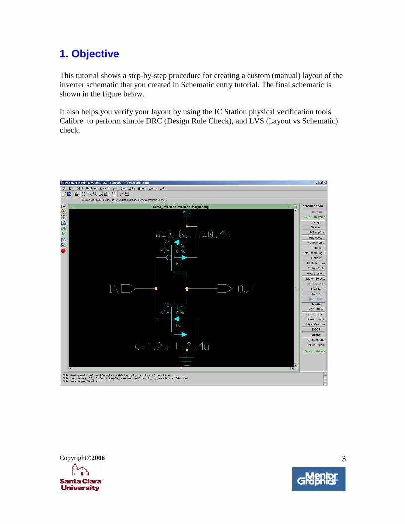
1. Objective
This tutorial shows a step-by-step procedure for creating a custom (manual) layout of the
inverter schematic that you created in Schematic entry tutorial. The final schematic is
shown in the figure below.
It also helps you verify your layout by using the IC Station physical verification tools
Calibre to perform simple DRC (Design Rule Check), and LVS (Layout vs Schematic)
check.

Copyright©2006
4
2. Setup & Preparation
The set of directives listed below is applicable to users of the Engineering Design Center
at Santa Clara University. If you are working in a different environment please check
with your system administrator.
The steps below are necessary only for the first time to setup the Mentor Graphics
environment by changing the settings in your .profile file.
Add the following lines in your .profile:
setup mentor-2008.1
alias swd=”export MGC_WD=\’pwd\’”
Remember to execute
$ . .profile

Copyright©2006
5
3. Launching IC Studio
On the command line
To Create a directory to contain your projects type:
“mkdir Tutorial”
To change the current directory to Tutorial type:
“cd Tutorial”.
To open ICSTUDIO type:
“icstudio”.
This launches the ICStudio window shown below.

Copyright©2006
6
4. Opening the project To create a project the follow the three steps given below:
1. Opening icstudio and opening the project
On the ICStudio Window
Click File -> Open -> Project to create a new project.
Enter the Project name (e.g vlsi_tutorial) and the Project Location
Click Open in the Open Project pop-up window
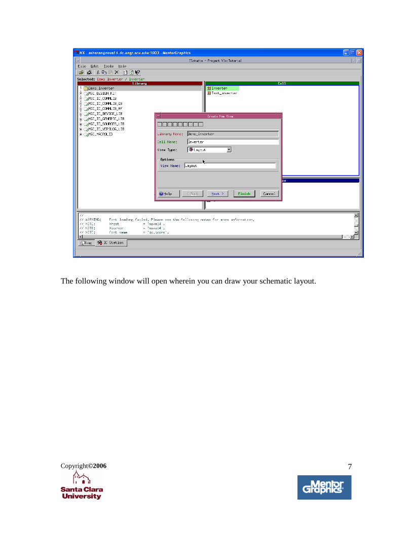
2. Opening Layout Cell
Right click on the name of the Schematic you entered (eg.; Inverter) and click
New View.
Select View Type as Layout.
Click Finish.
Copyright©2006
7
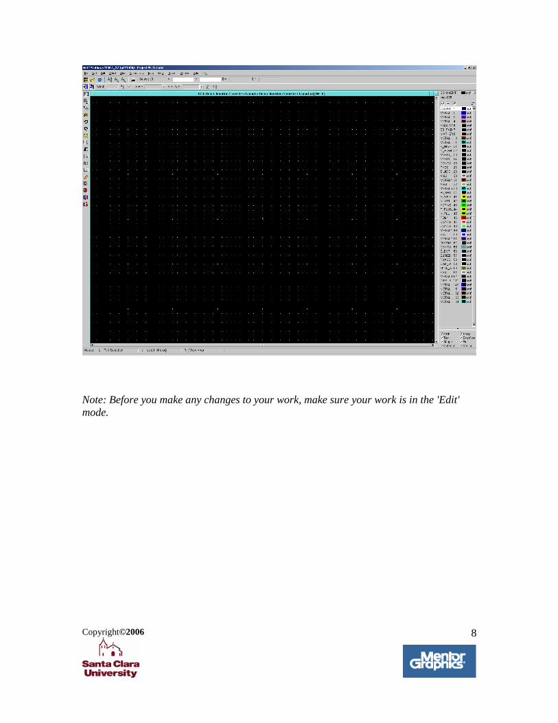
The following window will open wherein you can draw your schematic layout.
Copyright©2006
8
Note: Before you make any changes to your work, make sure your work is in the 'Edit'
mode.
Copyright©2006
9
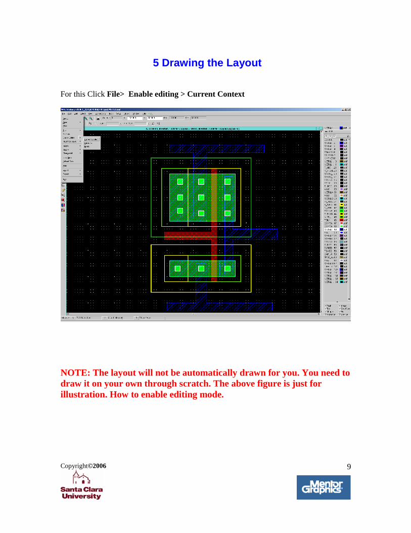
5 Drawing the Layout
For this Click File> Enable editing > Current Context
NOTE: The layout will not be automatically drawn for you. You need to
draw it on your own through scratch. The above figure is just for
illustration. How to enable editing mode.
Copyright©2006
10
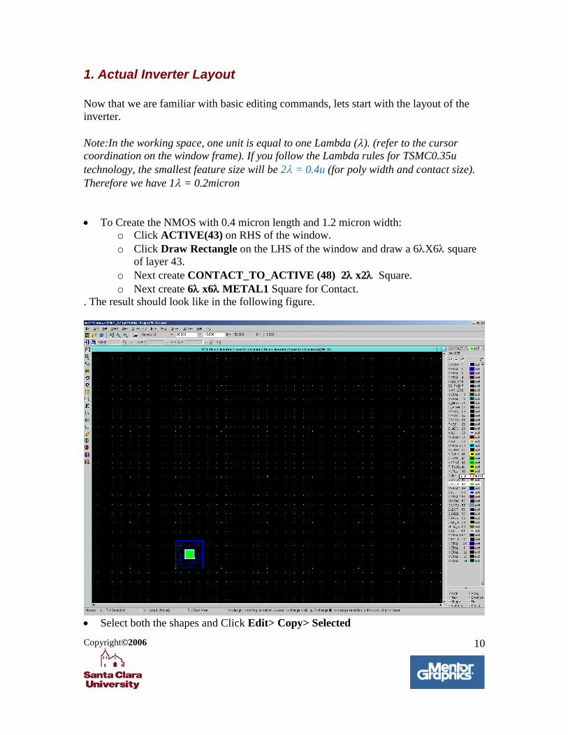
1. Actual Inverter Layout
Now that we are familiar with basic editing commands, lets start with the layout of the
inverter.
Note:In the working space, one unit is equal to one Lambda (). (refer to the cursor
coordination on the window frame). If you follow the Lambda rules for TSMC0.35u
technology, the smallest feature size will be 2 = 0.4u (for poly width and contact size).
Therefore we have 1 = 0.2micron
To Create the NMOS with 0.4 micron length and 1.2 micron width:
o Click ACTIVE(43) on RHS of the window.
o Click Draw Rectangle on the LHS of the window and draw a 6X6 square
of layer 43.
o Next create CONTACT_TO_ACTIVE (48) 2 x2 Square.
o Next create 6 x6 METAL1 Square for Contact.
. The result should look like in the following figure.
Select both the shapes and Click Edit> Copy> Selected

Copyright©2006
11
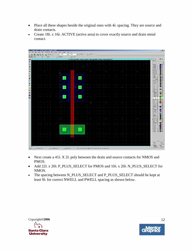
Next Click Edit> Paste
Place all these shapes beside the original ones with 4 spacing. They are source and
drain contacts.
Create 6 x 16 ACTIVE (active area) to cover exactly source and drain metal
contact.
Next
To Make the PMOS:
o Click ACTIVE(43) on RHS of the window.
o Click Draw Rectangle on the LHS of the window and draw a 6X6 square
of layer 43.
o Next create CONTACT_TO_ACTIVE (48) 2 x2 Square.
o Next create 18 x6 METAL1 Square for Contact.
Note: Distance between the NMOS and the PMOS should be at least 13
Select all the shapes and Click Edit> Copy> Selected
Next Click Edit> Paste
Copyright©2006
12
Place all these shapes beside the original ones with 4 spacing. They are source and
drain contacts.
Create 18 x 16 ACTIVE (active area) to cover exactly source and drain metal
contact.
Next create a 41 X 2 poly between the drain and source contacts for NMOS and
PMOS.
Add 22 x 20 P_PLUS_SELECT for PMOS and 10 x 20 N_PLUS_SELECT for
NMOS.
The spacing between N_PLUS_SELECT and P_PLUS_SELECT should be kept at
least 9 for correct NWELL and PWELL spacing as shown below.

Copyright©2006
13
Note: It is always better to add as many CONTACTS as possible to reduce the
contact resistance. So add 3 contacts in the Source area of PMOS (with 3 distance in between the contacts) and 4 contacts in the drain area of PMOS (with
2 distance in between the contacts) as shown in the adjacent figure. Note: As per the design rules of TSMC0.35, minimum separation between two
contacts should be 3.
Add 30 x 28 NWELL for PMOS and 18 x 28 PWELL for NMOS. The spacing
between NWELL and PWELL should be at least 1.
Copyright©2006
14
Add METAL1: to form Vdd (power wire) and GND (ground wire). Note that
METAL1 should have at least 3 width and 3 spacing (METAL1 to METAL1
spacing).
Now, connect PMOS-source to Vdd and that of NMOS to GND with METAL1.
(Use 'Notch’ – For this select the shape you want to notch or connect and click Edit->
Notch – Use your Left Mouse Button to alter Move the shape as desired and when you
are done press Escape)
Connect the drains of both transistors by METAL1, to get OUTPUT net of the
inverter.

Copyright©2006
15
The figure when you have notched the Vdd, GND and POLY would look as under:
Copyright©2006
16
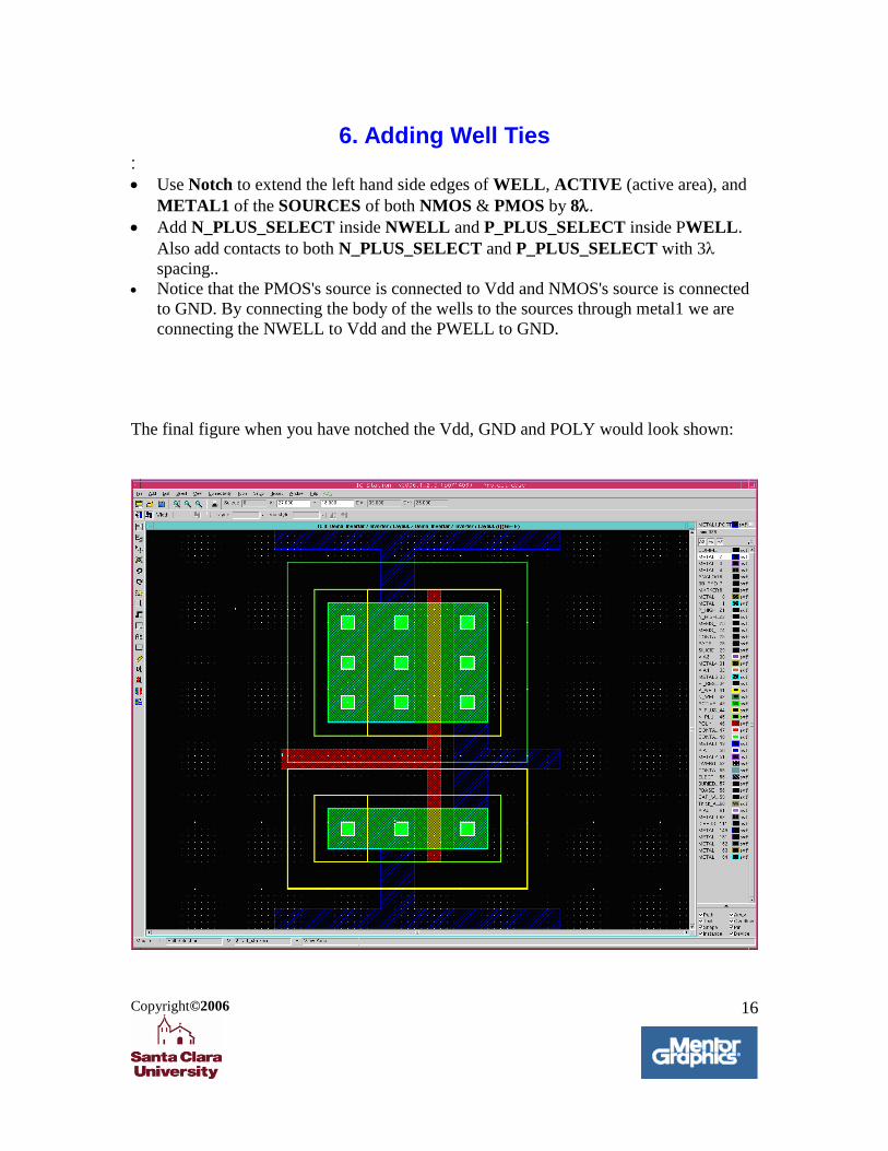
6. Adding Well Ties :
Use Notch to extend the left hand side edges of WELL, ACTIVE (active area), and
METAL1 of the SOURCES of both NMOS & PMOS by 8.
Add N_PLUS_SELECT inside NWELL and P_PLUS_SELECT inside PWELL.
Also add contacts to both N_PLUS_SELECT and P_PLUS_SELECT with 3
spacing..
Notice that the PMOS's source is connected to Vdd and NMOS's source is connected
to GND. By connecting the body of the wells to the sources through metal1 we are
connecting the NWELL to Vdd and the PWELL to GND.
The final figure when you have notched the Vdd, GND and POLY would look shown:

Copyright©2006
17
7. Making Ports
We will use METAL1 for all ports, so the first thing we must do is route the POLY gate
to a suitable METAL1 trace.
Select CONTACT TO POLY (47) from the RHS layer palette.
Create a 2 x 2 square of CONTACT TO POLY on the left side of the POLY
Select the POLY trace and use the NOTCH tool to surround the contact by 2 on
each side.
Add a square of METAL1 over the POLY/CONTACT TO POLY pad
The figure should look like the drawing below:

Copyright©2006
18
Labeling Ports:
Click on the top Metal polygon (Drain of the PMOS) to select it.
From main menu bar, select Connectivity -> Port -> Make Port:
For the Port Name, enter VDD. Make sure the Port Type is Signal and
Direction is in. Then click OK
Repeat the steps above to assign GND, IN and OUT ports.
Note: 'GND' and 'IN' are of 'in' Direction while 'OUT' is of 'out' Direction.

Copyright©2006
19
Select METAL1.PORT (2) on RHS of the window.
Select, from main Menu Bar, Add -> Text Enter the label VDD and place the text object on the VDD metal line.
Repeat for the OUT, GROUND, and IN metal lines.
Note: Be sure to label the GND port as GROUND. This name is required for
the LVS check to work correctly.
Copyright©2006
20
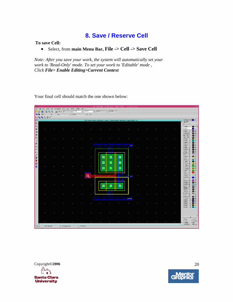
8. Save / Reserve Cell To save Cell:
Select, from main Menu Bar, File -> Cell -> Save Cell
Note: After you save your work, the system will automatically set your
work to 'Read-Only' mode. To set your work to 'Editable' mode ,
Click File> Enable Editing>Current Context
Your final cell should match the one shown below:

Copyright©2006
21
9. DRC/LVS
To Run DRC:
File Cell Set Logic Source
Mentor Graphics window Pops up
Select Schematic OK
Copyright©2006
22
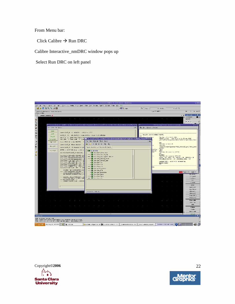
From Menu bar:
Click Calibre Run DRC
Calibre Interactive_nmDRC window pops up
Select Run DRC on left panel

Copyright©2006
23
LVS:
From Menu Bar:
Click on Calibre Run LVS
Copyright©2006
24
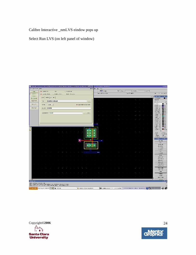
Calibre Interactive _nmLVS eindow pops up
Select Run LVS (on left panel of window)

Copyright©2006
25
If your LVS pass out you get a smiley on the caliber_LVS RVE window as shown below.