SCG2540 Synchronous Clock Generators - … Synchronous Clock Generators US Headquarters: ......
12
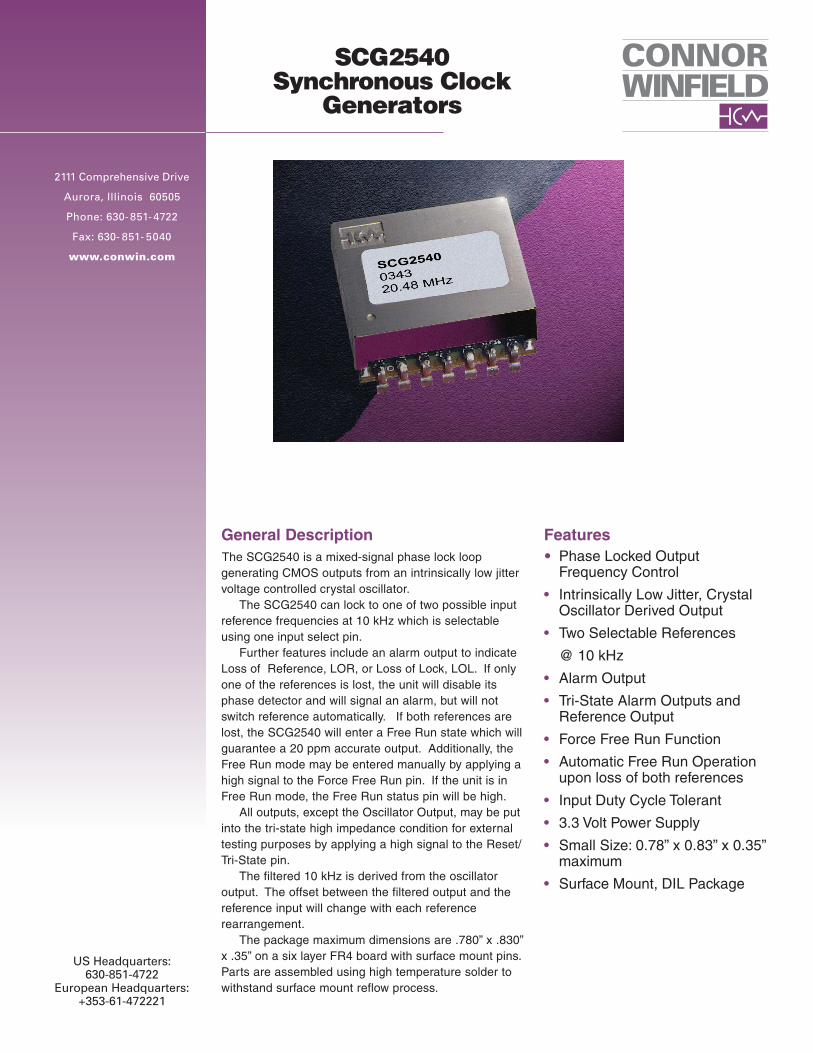
2111 Comprehensive Drive Aurora, Illinois 60505 Phone: 630-851-4722 Fax: 630- 851- 5040 www.conwin.com SCG2540 Synchronous Clock Generators US Headquarters: 630-851-4722 European Headquarters: +353-61-472221 General Description The SCG2540 is a mixed-signal phase lock loop generating CMOS outputs from an intrinsically low jitter voltage controlled crystal oscillator. The SCG2540 can lock to one of two possible input reference frequencies at 10 kHz which is selectable using one input select pin. Further features include an alarm output to indicate Loss of Reference, LOR, or Loss of Lock, LOL. If only one of the references is lost, the unit will disable its phase detector and will signal an alarm, but will not switch reference automatically. If both references are lost, the SCG2540 will enter a Free Run state which will guarantee a 20 ppm accurate output. Additionally, the Free Run mode may be entered manually by applying a high signal to the Force Free Run pin. If the unit is in Free Run mode, the Free Run status pin will be high. All outputs, except the Oscillator Output, may be put into the tri-state high impedance condition for external testing purposes by applying a high signal to the Reset/ Tri-State pin. The filtered 10 kHz is derived from the oscillator output. The offset between the filtered output and the reference input will change with each reference rearrangement. The package maximum dimensions are .780” x .830” x .35” on a six layer FR4 board with surface mount pins. Parts are assembled using high temperature solder to withstand surface mount reflow process. Features • Phase Locked Output Frequency Control • Intrinsically Low Jitter, Crystal Oscillator Derived Output • Two Selectable References @ 10 kHz • Alarm Output • Tri-State Alarm Outputs and Reference Output • Force Free Run Function • Automatic Free Run Operation upon loss of both references • Input Duty Cycle Tolerant • 3.3 Volt Power Supply • Small Size: 0.78” x 0.83” x 0.35” maximum • Surface Mount, DIL Package
Transcript of SCG2540 Synchronous Clock Generators - … Synchronous Clock Generators US Headquarters: ......
2111 Comprehensive Drive
Aurora, Illinois 60505
Phone: 630- 851- 4722
Fax: 630- 851- 5040
www.conwin.com
SCG2540Synchronous Clock
Generators
US Headquarters:630-851-4722
European Headquarters:+353-61-472221
General DescriptionThe SCG2540 is a mixed-signal phase lock loopgenerating CMOS outputs from an intrinsically low jittervoltage controlled crystal oscillator.
The SCG2540 can lock to one of two possible inputreference frequencies at 10 kHz which is selectableusing one input select pin.
Further features include an alarm output to indicateLoss of Reference, LOR, or Loss of Lock, LOL. If onlyone of the references is lost, the unit will disable itsphase detector and will signal an alarm, but will notswitch reference automatically. If both references arelost, the SCG2540 will enter a Free Run state which willguarantee a 20 ppm accurate output. Additionally, theFree Run mode may be entered manually by applying ahigh signal to the Force Free Run pin. If the unit is inFree Run mode, the Free Run status pin will be high.
All outputs, except the Oscillator Output, may be putinto the tri-state high impedance condition for externaltesting purposes by applying a high signal to the Reset/Tri-State pin.
The filtered 10 kHz is derived from the oscillatoroutput. The offset between the filtered output and thereference input will change with each referencerearrangement.
The package maximum dimensions are .780” x .830”x .35” on a six layer FR4 board with surface mount pins.Parts are assembled using high temperature solder towithstand surface mount reflow process.
Features• Phase Locked Output
Frequency Control
• Intrinsically Low Jitter, CrystalOscillator Derived Output
• Two Selectable References
@ 10 kHz
• Alarm Output
• Tri-State Alarm Outputs andReference Output
• Force Free Run Function
• Automatic Free Run Operationupon loss of both references
• Input Duty Cycle Tolerant
• 3.3 Volt Power Supply
• Small Size: 0.78” x 0.83” x 0.35”maximum
• Surface Mount, DIL Package

Preliminary Data Sheet #: SG049 Page 2 of 12 Rev: P01 Date: 11/11/03
© Copyright 2003 The Connor-Winfield Corp. All Rights Reserved Specifications subject to change without notice
Operating SpecificationsTable 2
Parameter Specifications Notes
Voltage 3.3V ±5% 1.0
Current 100 mA Typical
Oscillator Output Frequencies 20.48 MHz
Temperature Range 0 to 70°C
Input Frequency Ref 1 and Ref 2 10 kHz 2.0
Input Jitter Tolerance ≥ 1µs Typical(Jitter Frequencies > 10 Hz)
Jitter Bandwidth < 10 Hz
Typical Acquisition Time Data
Acquisition from a cold power-up: Phase lock settled: 30 - 60s Alarm time: <1.0s TypicalAcquisition from Free Run: Phase lock settled: 30 - 60s Alarm time: <1.0s TypicalFrequency lock with a 20PPM reference frequency step: Typically 0.5s.Phase lock during a switch between equal frequency references: Typically 0.5s, no alarm should be issued
Capture/Pull-In Range ± 25 ppm Minimum
Output Duty Cycle 40/60 % Min/Max @ 50% Level
Output Rise and Fall Time 3 nS @ 20% to 80% output level
Output Load 30 pF
Alarm LOR/LOL Status Signal Output
Free Run Accuracy ±20 ppm
Package Fr4 SM 0.78” x 0.83” x 0.350” (Maximum)
MTIE @ Synchronization Rearrangement GR-253-CORE, 1999 R5-136 3.0, 4.0
Absolute Maximum RatingTable 1
Symbol Parameter Minimum Nominal Maximum Units Notes
VCC Power Supply Voltage -0.5 - +4.0 Volts
VI Input Voltage -0.5 - +5.5 Volts
TS Storage Temperature -65.0 - +150.0 °C
Input and Output CharacteristicsTable 3
Symbol Parameter Minimum Nominal Maximum Units Notes
VIH High level input voltage 2.0 - 5.5 V
VIL Low level input voltage 0 - 0.8 V
TIO I/O to output valid - - 10 nS
COUT Output capacitance - - 10 pF
VHO High level output voltage loh = -4mA 2.40 - - - Vcc Min
VIO Low Level output voltage lo1 = 8mA - - 0.4 - Vcc Max
TIR Input reference signal pulse width 30 - - nS

Preliminary Data Sheet #: SG049 Page 3 of 12 Rev: P01 Date: 11/11/03
© Copyright 2003 The Connor-Winfield Corp. All Rights Reserved Specifications subject to change without notice
Input Selection / Output ResponseTable 5
INPUTS OUPUTSReset/ Oscillator 10 kHz NotesTri-State SEL
ABREF
AREF
BFR FR
statusAlarm Output Output
1 X X X X TS TS FR TS
0 X X X 1 1 1 FR FR
0 0 A A 0 0 0 LRA LRAD
0 1 NA A 0 0 0 LRB LRBD
0 0 NA A 0 0 1 U U 5.0
0 1 A NA 0 0 1 U U 5.0
0 0 A NA 0 0 0 LRA LRAD
0 X NA NA 0 1 1 FR FR
NOTES:1.0 Requires external regulation2.0 Externally selectable via Input Select AB3.0 Entry into Free Run doesn’t meet requirement for initial 2.33 seconds of self-timing4.0 If the selected reference is removed, system response to the ALARM must be less than 100ns5.0 On alarm assertion, switch references. If alarm is still active, force Free Run
A = Active NA = Not Active or Not PresentTS = Tri-State U = UnstableFR = Free Run LRAD = Locked to Ref A and divided downLRA = Locked to Ref A LRAB = Locked to ref B and divided downLRB = Locked to Reb B X = Don’t care
Output Jitter SpecificationsTable 4
Jitter BW 10 Hz - 1 MHz SONET Jitter BW 12 kHz - 20 MHzFrequency (MHz) pS (RMS) m UI pS (RMS) m UI
20.48 10 Typ. 0.205 Typ. 1 Max., 0.5 Typ. 0.020 Max.

Preliminary Data Sheet #: SG049 Page 4 of 12 Rev: P01 Date: 11/11/03
© Copyright 2003 The Connor-Winfield Corp. All Rights Reserved Specifications subject to change without notice
Circuit Board FootprintFigure 1
Pin Connection
1 Filtered 10 kHz Output
2 TCK
3 TMS
4 Ground
5 Force Free Run / TDI (1 = Free Run)
6 Alarm Output (1 = Alarm)
7 REF B
8 REF A
9 Oscillator Output
10 Free Run Status Output (FR = 1)
11 Vcc
12 TDO
13 Reset / Tri-State
14 Input Reference Select AB (A = 0, B = 1)
Pin ConnectionsTable 6
0.650
0.100 TYP
0.050 TYP
0.800
0.640
0.080
(16.51mm)
(1.27mm)(16.26mm)
(20.32mm)
(2.03mm)
0.050 TYP
(1.27mm)
(2.54mm)
10 kHz PHASEALIGNERREFB
REFA
SELECT AB
ANALOGFILTER
OSCILLATOROUTPUT
1 / N
ALARM OUTPUT
LOW JITTERVCXO
FORCEFREE RUN
FREE RUN STATUSOUTPUT
10 kHzOUTPUT
TRI-STATE/RESET
DPFD
0 Ω
10 kΩ
10 kΩ
2.2 kΩ
27 Ω
27 Ω
33 Ω
Block DiagramFigure 2

Preliminary Data Sheet #: SG049 Page 5 of 12 Rev: P01 Date: 11/11/03
© Copyright 2003 The Connor-Winfield Corp. All Rights Reserved Specifications subject to change without notice
Package Maximum DimensionsFigure 3

Preliminary Data Sheet #: SG049 Page 6 of 12 Rev: P01 Date: 11/11/03
© Copyright 2003 The Connor-Winfield Corp. All Rights Reserved Specifications subject to change without notice
Start-up Region
1 2 3 4 5
10 kHz Input Reference
< 1.0 µsec
1.0 µsec
> 1.0 µsec
100 Min to 300 Max µsec wide range
Minimum pulse width = 2 µsec
During Start-up, The LOL Alarm will pulse during the first few seconds of operation.
Loss of Reference Condition Alarm TimingFigure 4
AlarmTiming LegendUse for all alarm timing diagramsTable 7
LOL (Internal Signal)
Phase Detector(Internal Signal)
External Reference(Selected Input A or B)
Internal Reference(Internal Signal)
LOR (Internal Signal) 4
2 2 2 2 2 2 2 2 2 2 2 2 2 2
3
2
Start-upRegion
1 1
Alarm Output(LOR + LOL)

Preliminary Data Sheet #: SG049 Page 7 of 12 Rev: P01 Date: 11/11/03
© Copyright 2003 The Connor-Winfield Corp. All Rights Reserved Specifications subject to change without notice
Loss of Lock Condition Alarm TimingFigure 5
LOL (Internal Signal)
Phase Detector(Internal Signal)
External Reference(Selected Input A or B)
Internal Reference(Internal Signal)
LOR (Internal Signal)
33
22222 222 2 2
11 1 1
2 2 2 2
1
5
Alarm Output(LOR + LOL)

Preliminary Data Sheet #: SG049 Page 8 of 12 Rev: P01 Date: 11/11/03
© Copyright 2003 The Connor-Winfield Corp. All Rights Reserved Specifications subject to change without notice
MEETS EIA-481A AND EIAJ-1009B
1.00 DIA
250 PCS/REEL MAXIMUM
.083.15
13.00
8.45 DIA
.08
1.31
.08
DIRECTION OF FEED (CUSTOMER)
(33.27mm)
(2.0mm)(2.0mm)
(330.2mm)
(80mm)(2.0mm)
(214.6mm) DIA
(25.4mm)
(Bo)
POCKET SIZE
(Ao)
(Ko)
20.92mm (.824")
21.17mm (.833")
9.49mm (.374")
32mm (1.26") WIDTH
32mm (1.26") PITCH
6.99mm (.275")(KI)
.374
3°
AD
(9.49mm)
.014
(.36mm)
(28.4mm)
1.118
.559
(14.2mm)
.079 (2mm) DIA. MIN.
.059 (1.5mm) DIA.
.063 (1.6mm) DIA.
.069(1.75mm)
(4mm)
.157
(2mm)
.079
.063 (1.6mm)
.059 (1.5mm).065
.072 (1.85mm)
(1.65mm)
(Ko)
(20.92mm)
.824
.833 (Bo)
(21.17mm)
BD
3°
1.26
(32.0mm)
.275
(6.99mm)
1.260 (32.0mm).236 (6.0mm)
(1.93mm).076
45° 19.4°
.383
(9.74mm)
(6.00mm)
.236
(3.00mm)
.118
.138
(3.51mm)
W
P
Tape and Reel PackagingFigure 6

Preliminary Data Sheet #: SG049 Page 9 of 12 Rev: P01 Date: 11/11/03
© Copyright 2003 The Connor-Winfield Corp. All Rights Reserved Specifications subject to change without notice
Temp
0
100
150
200
250
50
1 2 3 4 5 6 7 8
Time (minutes)
(Deg C)
Recommended Reflow Profile
Peak Temp: 217 Deg CMax Rise Slope: 1.5 DegC/SecTime Above 150 C: 100 Sec
Solder ProfileFigure 7
Ordering Information
SCGXXXX-FFF.FFFM
XXXX equals a specific model (2540)FFF.FFF equals the Oscillator Output frequency (020.48)
M equals MHZ and is added to all part numbers
Example: To order an SCG2540 with an Oscillator Output of 20.48 MHz,Order part number SCG2540-020.48M
Please contact Connor-Winfield for other frequencies that may be available.

Preliminary Data Sheet #: SG049 Page 10 of 12 Rev: P01 Date: 11/11/03
© Copyright 2003 The Connor-Winfield Corp. All Rights Reserved Specifications subject to change without notice
Model Comparison TableTable 1
MaxModel Input Duty Reference Output Oscillator Output Notes
Ref Freq Cycle (Synchronized Output)
SCG2500 2@8kHz 40/60 8 kHz 1.544 MHz - 77.76 MHz
SCG2520 [email protected] MHz 40/60 19.44 MHz 19.44 MHz
SCG2540 2@10 kHz 40/60 10 kHz 20.48 MHz
SCG2550 2@8 kHz 40/60 19.44 MHz 19.44 - 77.76 MHz
SCG2560 2@25 MHz 45/55 25 MHz 125 MHz
Other low jitter line card solutions from Connor-WinfieldSCG51 Series Single input, jitter filtered with Free Run, 1 CMOS and 3 LVPECL outputs up to 622.08 MHz.
SCG102A/104A Single input, frequency selectable, LVPECL clock smoothers from 77.76 to 777.76 MHz.
SCG2000 Series Single input, jitter filtered with 20ppm Free Run, CMOS outputs from 8 kHz to 125.0 MHz.
SCG3000 Series Single input, jitter filtered with Dual LVPECL outputs.
SCG4000 Series Single input, jitter filtered with 20ppm Free Run, LVPECL outputs from 77.76 MHz to 180 MHz.
SCG4500 Series Dual input, jitter filtered with Free Run, 1 LVPECL differential pair output up to 622.08 MHz.
SCG4600 Series Dual input, jitter filtered with Free Run, 1 CML differential pair output up to 622.08 MHz.

Preliminary Data Sheet #: SG049 Page 11 of 12 Rev: P01 Date: 11/11/03
© Copyright 2003 The Connor-Winfield Corp. All Rights Reserved Specifications subject to change without notice

Revision Revision Date Note
P00 5/16/02 Preliminary Product Release
P01 11/11/03 Revised Typ. Acquisition Time in Tbl. 2