SCC2691 3 Universal asynchronous … asynchronous receiver/transmitter (UART) ... The baud rate...
25
Philips Semiconductors SCC2691 Universal asynchronous receiver/transmitter (UART) Product data sheet Supersedes data of 1998 Sep 04 2006 Aug 04 INTEGRATED CIRCUITS
Transcript of SCC2691 3 Universal asynchronous … asynchronous receiver/transmitter (UART) ... The baud rate...
SCC2691Universal asynchronousreceiver/transmitter (UART)
Product data sheetSupersedes data of 1998 Sep 04
2006 Aug 04
INTEGRATED CIRCUITS
Philips Semiconductors Product data sheet
SCC2691Universal asynchronous receiver/transmitter (UART)
22006 Aug 04
DESCRIPTIONThe Philips Semiconductors SCC2691 Universal AsynchronousReceiver/Transmitter (UART) is a single-chip CMOS-LSIcommunications device that provides a full-duplex asynchronousreceiver/transmitter. It is fabricated with Philips SemiconductorsCMOS technology which combines the benefits of high density andlow power consumption.
The operating speed of the receiver and transmitter can be selectedindependently as one of 18 fixed baud rates, a 16X clock derivedfrom a programmable counter/timer, or an external 1X or 16X clock.The baud rate generator and counter/timer can operate directly froma crystal or from external clock inputs. The ability to independentlyprogram the operating speed of the receiver and transmitter makethe UART particularly attractive for dual-speed channel applicationssuch as clustered terminal systems.
The receiver is quadruple buffered to minimize the potential ofreceiver overrun or to reduce interrupt overhead in interrupt drivensystems. In addition, a handshaking capability is provided to disablea remote UART transmitter when the receiver buffer is full.
The UART provides a power-down mode in which the oscillator isfrozen but the register contents are stored. This results in reducedpower consumption on the order of several magnitudes.
The UART is fully TTL compatible and operates from a single +5Vpower supply.
FEATURES• Full-duplex asynchronous receiver/transmitter
• Quadruple buffered receiver data register
• Programmable data format:
– 5 to 8 data bits plus parity
– Odd, even, no parity or force parity
– 1, 1.5 or 2 stop bits programmable in 1/16-bit increments
• 16-bit programmable Counter/Timer
• Baud rate for the receiver and transmitter selectable from:
– 22 fixed rates: 50 to 115.2K baud
– Non-standard rates to 115.2 kb
– Non-standard user-defined rate derived from programmabletimer/ counter
– External 1X or 16X clock
• Parity, framing, and overrun detection
• False start bit detection
• Line break detection and generation
• Programmable channel mode
– Normal (full-duplex)
– Automatic echo
– Local loopback
– Remote Loopback
• Multi-function programmable 16-bit counter/timer
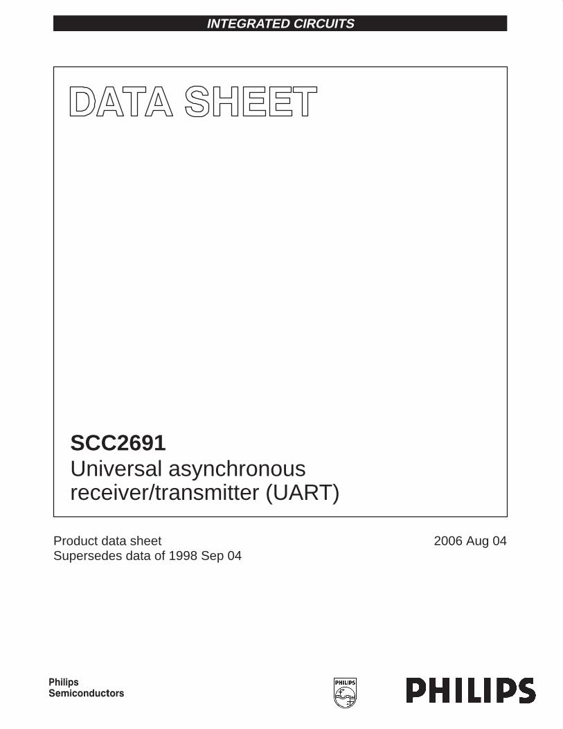
PIN CONFIGURATIONS
1
2
3
4
5
6
7
8
9
10
11
12
23
22
21
20
19
18
17
16
15
14
13
RDN
RxD
TxD
MPO
MPI
A2
A1
A0
X1/CLK
X2
RESET
GND
4 1 26
25
19
1812
11
5
N24ANDD24
PACKAGES
A28PACKAGE
24 VCC
WRN
D0
D1
D2
D3
D4
D5
D6
D7
CEN
INTRN
Pin Symbol Pin Symbol
VCCRDNRxDTxDMPOMPINCNCA2A1A0X1/CLKX2RESET
1234567891011121314
1516171819202122232425262728
GNDINTRNCEND7D6D5D4D3NCD2D1NCD0WRN
SD00122
Figure 1. Pin Configurations
• Single interrupt output with seven maskable interruptingconditions
• On-chip crystal oscillator
• Low power mode
• TTL compatible
• Single +5V power supply
• Commercial (0°C to +70°C) and industrial (-40°C to +85°C)temperature versions available
• SOL, PLCC and 300 mil wide DIP packages available
Philips Semiconductors Product data sheet
SCC2691Universal asynchronous receiver/transmitter (UART)
2006 Aug 04 3
ORDERING INFORMATIONCOMMERCIAL INDUSTRIAL
PACKAGES VCC = +5V +10%, TA = 0°C to +70°C
VCC = +5V +10%, TA = –40°C to +85°C
VERSION
24-Pin Plastic Dual In-Line Package (DIP) SCC2691AC1N24 SCC2691AE1N24 SOT222–1
28-Pin Plastic Leaded Chip Carrier (PLCC) Package SCC2691AC1A28 SCC2691AE1A28 SOT261-2
24-Pin Plastic Small Outline Large (SOL) Package SCC2691AC1D24 SOT137-1
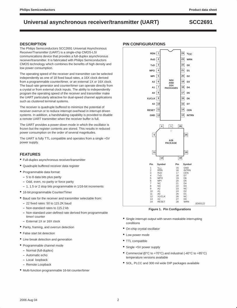
BLOCK DIAGRAM
8
D0–D7
RDN
WRN
CEN
A0–A2
RESET
INTRN
X1/CLK
X2
TIMING
CONTROL
INTERNAL DATABUS
3
BUS BUFFER
OPERATION CONTROL
ADDRESSDECODE
R/W CONTROL
INTERRUPT CONTROL
IMR
ISR
TIMING
BAUD RATEGENERATOR
CLOCKSELECTORS
COUNTER/TIMER
CRYSTALOSCILLATOR
POWER DOWNLOGIC
CSR
ACR
CTUR
CTLR
CHANNEL A
TRANSMITHOLDING REG
TRANSMITSHIFT REGISTER
RECEIVEHOLDING REG (3)
RECEIVESHIFT REGISTER
MR1, 2
CR
SR
INPUT PIN
CHANGE OFSTATE
DETECTOR
OUTPUT PIN
FUNCTIONSELECT LOGIC
ACR
TxD
RxD
MPI
MPO
VCC
GND
SD00123
Figure 2. Block Diagram
Philips Semiconductors Product data sheet
SCC2691Universal asynchronous receiver/transmitter (UART)
2006 Aug 04 4
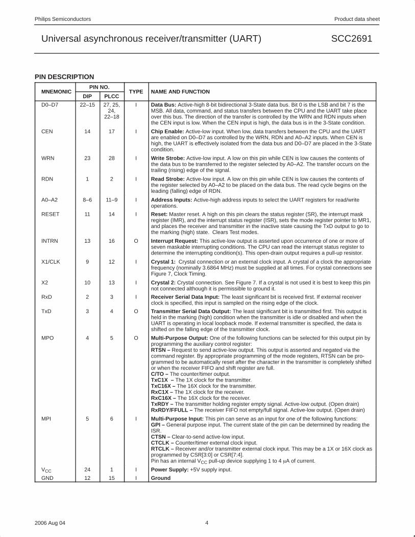
PIN DESCRIPTION
MNEMONICPIN NO.
TYPE NAME AND FUNCTIONMNEMONICDIP PLCC
TYPE NAME AND FUNCTION
D0–D7 22–15 27, 25,24,
22–18
I Data Bus: Active-high 8-bit bidirectional 3-State data bus. Bit 0 is the LSB and bit 7 is theMSB. All data, command, and status transfers between the CPU and the UART take placeover this bus. The direction of the transfer is controlled by the WRN and RDN inputs whenthe CEN input is low. When the CEN input is high, the data bus is in the 3-State condition.
CEN 14 17 I Chip Enable: Active-low input. When low, data transfers between the CPU and the UARTare enabled on D0–D7 as controlled by the WRN, RDN and A0–A2 inputs. When CEN ishigh, the UART is effectively isolated from the data bus and D0–D7 are placed in the 3-Statecondition.
WRN 23 28 I Write Strobe: Active-low input. A low on this pin while CEN is low causes the contents ofthe data bus to be transferred to the register selected by A0–A2. The transfer occurs on thetrailing (rising) edge of the signal.
RDN 1 2 I Read Strobe: Active-low input. A low on this pin while CEN is low causes the contents ofthe register selected by A0–A2 to be placed on the data bus. The read cycle begins on theleading (falling) edge of RDN.
A0–A2 8–6 11–9 I Address Inputs: Active-high address inputs to select the UART registers for read/writeoperations.
RESET 11 14 I Reset: Master reset. A high on this pin clears the status register (SR), the interrupt maskregister (IMR), and the interrupt status register (ISR), sets the mode register pointer to MR1,and places the receiver and transmitter in the inactive state causing the TxD output to go tothe marking (high) state. Clears Test modes.
INTRN 13 16 O Interrupt Request: This active-low output is asserted upon occurrence of one or more ofseven maskable interrupting conditions. The CPU can read the interrupt status register todetermine the interrupting condition(s). This open-drain output requires a pull-up resistor.
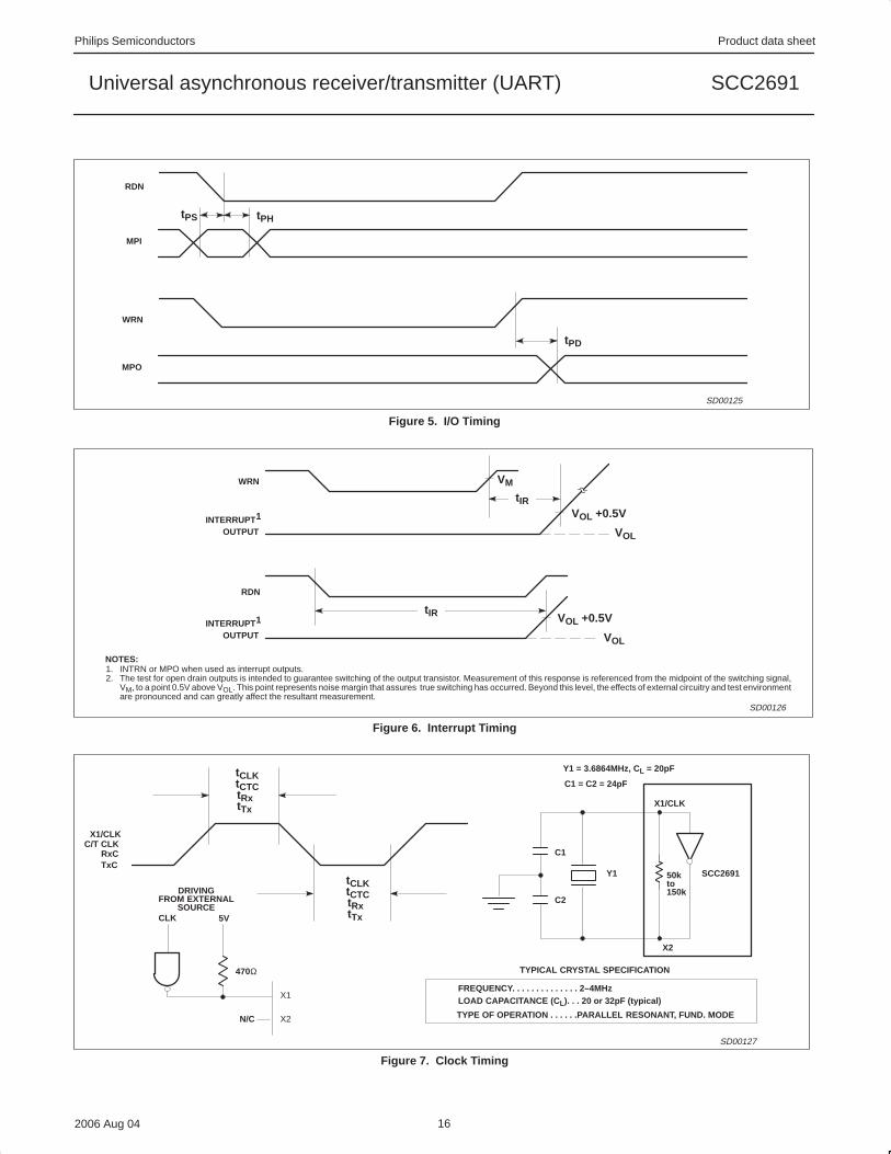
X1/CLK 9 12 I Crystal 1: Crystal connection or an external clock input. A crystal of a clock the appropriatefrequency (nominally 3.6864 MHz) must be supplied at all times. For crystal connections seeFigure 7, Clock Timing.
X2 10 13 I Crystal 2: Crystal connection. See Figure 7. If a crystal is not used it is best to keep this pinnot connected although it is permissible to ground it.
RxD 2 3 I Receiver Serial Data Input: The least significant bit is received first. If external receiverclock is specified, this input is sampled on the rising edge of the clock.
TxD 3 4 O Transmitter Serial Data Output: The least significant bit is transmitted first. This output isheld in the marking (high) condition when the transmitter is idle or disabled and when theUART is operating in local loopback mode. If external transmitter is specified, the data isshifted on the falling edge of the transmitter clock.
MPO 4 5 O Multi-Purpose Output: One of the following functions can be selected for this output pin byprogramming the auxiliary control register:RTSN – Request to send active-low output. This output is asserted and negated via thecommand register. By appropriate programming of the mode registers, RTSN can be pro-grammed to be automatically reset after the character in the transmitter is completely shiftedor when the receiver FIFO and shift register are full.C/TO – The counter/timer output.TxC1X – The 1X clock for the transmitter.TxC16X – The 16X clock for the transmitter.RxC1X – The 1X clock for the receiver.RxC16X – The 16X clock for the receiver.TxRDY – The transmitter holding register empty signal. Active-low output. (Open drain)RxRDY/FFULL – The receiver FIFO not empty/full signal. Active-low output. (Open drain)
MPI 5 6 I Multi-Purpose Input: This pin can serve as an input for one of the following functions:GPI – General purpose input. The current state of the pin can be determined by reading theISR.CTSN – Clear-to-send active-low input.CTCLK – Counter/timer external clock input.RTCLK – Receiver and/or transmitter external clock input. This may be a 1X or 16X clock asprogrammed by CSR[3:0] or CSR[7:4].Pin has an internal VCC pull-up device supplying 1 to 4 A of current.
VCC 24 1 I Power Supply: +5V supply input.
GND 12 15 I Ground
Philips Semiconductors Product data sheet
SCC2691Universal asynchronous receiver/transmitter (UART)
2006 Aug 04 5
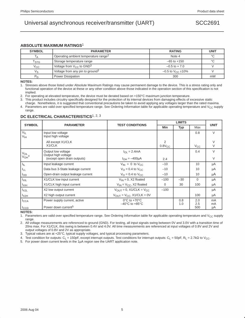
ABSOLUTE MAXIMUM RATINGS 1
SYMBOL PARAMETER RATING UNIT
TA Operating ambient temperature range2 Note 4 °CTSTG Storage temperature range –65 to +150 °CVCC Voltage from VCC to GND3 –0.5 to + 7.0 V
VS Voltage from any pin to ground3 –0.5 to VCC +10% V
PD Power Dissipation 300 mW
NOTES:1. Stresses above those listed under Absolute Maximum Ratings may cause permanent damage to the device. This is a stress rating only and
functional operation of the device at these or any other condition above those indicated in the operation section of this specification is notimplied.
2. For operating at elevated temperature, the device must be derated based on +150°C maximum junction temperature.3. This product includes circuitry specifically designed for the protection of its internal devices from damaging effects of excessive static
charge. Nonetheless, it is suggested that conventional precautions be taken to avoid applying any voltages larger than the rated maxima.4. Parameters are valid over specified temperature range. See Ordering Information table for applicable operating temperature and VCC supply
range.
DC ELECTRICAL CHARACTERISTICS 1, 2, 3
SYMBOL PARAMETER TEST CONDITIONSLIMITS
UNITSYMBOL PARAMETER TEST CONDITIONSMin Typ Max
UNIT
VILVIH
Input low voltageInput high voltage
0.8 V
All except X1/CLK X1/CLK
20.8VCC VCC
VV
VOLVOH
4
Output low voltageOutput high voltage (except open drain outputs)
IOL = 2.4mA
IOH = –400µA 2.4
0.4 V
V
IIL Input leakage current VIN = 0 to VCC –10 10 µA
ILL Data bus 3-State leakage current VO = 0.4 to VCC –10 10 µA
IOD Open-drain output leakage current VO = 0.4 to VCC –10 10 µAIXIL X1/CLK low input current VIN = 0, X2 floated –100 –30 0 µA
IXIH X1/CLK high input current VIN = VCC, X2 floated 0 30 100 µA
IX2L X2 low output current VOUT = 0, X1/CLK = VCC –100 µA
IX2H X2 high output current VOUT = VCC, X1/CLK = 0V 100 µA
ICCA
ICCD
Power supply current, active
Power down current5
0°C to +70°C–40°C to +85°C
0.81.0
2.02.5500
mAmAµA
NOTES:1. Parameters are valid over specified temperature range. See Ordering Information table for applicable operating temperature and VCC supply
range.2. All voltage measurements are referenced to ground (GND). For testing, all input signals swing between 0V and 3.0V with a transition time of
20ns max. For X1/CLK, this swing is between 0.4V and 4.0V. All time measurements are referenced at input voltages of 0.8V and 2V andoutput voltages of 0.8V and 2V as appropriate.
3. Typical values are at +25°C, typical supply voltages, and typical processing parameters.4. Test condition for outputs: CL = 150pF, except interrupt outputs. Test conditions for interrupt outputs: CL = 50pF, RL = 2.7kΩ to VCC.5. For power down current levels in the 1µA region see the UART application note.
Philips Semiconductors Product data sheet
SCC2691Universal asynchronous receiver/transmitter (UART)
2006 Aug 04 6
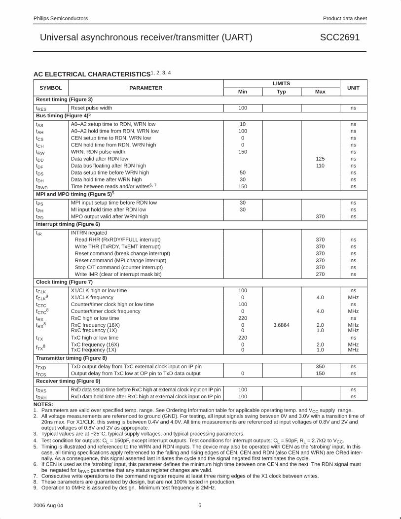
AC ELECTRICAL CHARACTERISTICS 1, 2, 3, 4
SYMBOL PARAMETERLIMITS
UNITSYMBOL PARAMETERMin Typ Max
UNIT
Reset timing (Figure 3)
tRES Reset pulse width 100 ns
Bus timing (Figure 4) 5
tAS A0–A2 setup time to RDN, WRN low 10 nstAH A0–A2 hold time from RDN, WRN low 100 nstCS CEN setup time to RDN, WRN low 0 nstCH CEN hold time from RDN, WRN high 0 nstRW WRN, RDN pulse width 150 nstDD Data valid after RDN low 125 nstDF Data bus floating after RDN high 110 nstDS Data setup time before WRN high 50 nstDH Data hold time after WRN high 30 nstRWD Time between reads and/or writes6, 7 150 ns
MPI and MPO timing (Figure 5) 5
tPS MPI input setup time before RDN low 30 nstPH MI input hold time after RDN low 30 nstPD MPO output valid after WRN high 370 ns
Interrupt timing (Figure 6)
tIR INTRN negatedRead RHR (RxRDY/FFULL interrupt) 370 nsWrite THR (TxRDY, TxEMT interrupt) 370 nsReset command (break change interrupt) 370 nsReset command (MPI change interrupt) 370 nsStop C/T command (counter interrupt) 370 nsWrite IMR (clear of interrupt mask bit) 270 ns
Clock timing (Figure 7)
tCLK X1/CLK high or low time 100 nsfCLK
9 X1/CLK frequency 0 4.0 MHztCTC Counter/timer clock high or low time 100 nsfCTC
8 Counter/timer clock frequency 0 4.0 MHztRX RxC high or low time 220 nsfRX
8 RxC frequency (16X)RxC frequency (1X)
00
3.6864 2.01.0
MHzMHz
tTX TxC high or low time 220 ns
fTX8 TxC frequency (16X)
TxC frequency (1X)00
2.01.0
MHzMHz
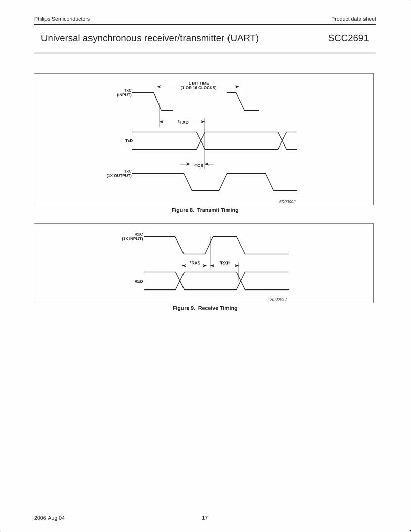
Transmitter timing (Figure 8)
tTXD TxD output delay from TxC external clock input on IP pin 350 nstTCS Output delay from TxC low at OP pin to TxD data output 0 150 ns
Receiver timing (Figure 9)
tRXS RxD data setup time before RxC high at external clock input on IP pin 100 nstRXH RxD data hold time after RxC high at external clock input on IP pin 100 ns
NOTES:1. Parameters are valid over specified temp. range. See Ordering Information table for applicable operating temp. and VCC supply range.2. All voltage measurements are referenced to ground (GND). For testing, all input signals swing between 0V and 3.0V with a transition time of
20ns max. For X1/CLK, this swing is between 0.4V and 4.0V. All time measurements are referenced at input voltages of 0.8V and 2V andoutput voltages of 0.8V and 2V as appropriate.
3. Typical values are at +25°C, typical supply voltages, and typical processing parameters.4. Test condition for outputs: CL = 150pF, except interrupt outputs. Test conditions for interrupt outputs: CL = 50pF, RL = 2.7kΩ to VCC.5. Timing is illustrated and referenced to the WRN and RDN inputs. The device may also be operated with CEN as the ‘strobing’ input. In this
case, all timing specifications apply referenced to the falling and rising edges of CEN. CEN and RDN (also CEN and WRN) are ORed inter-nally. As a consequence, this signal asserted last initiates the cycle and the signal negated first terminates the cycle.
6. If CEN is used as the ‘strobing’ input, this parameter defines the minimum high time between one CEN and the next. The RDN signal mustbe negated for tRWD guarantee that any status register changes are valid.
7. Consecutive write operations to the command register require at least three rising edges of the X1 clock between writes.8. These parameters are guaranteed by design, but are not 100% tested in production.9. Operation to 0MHz is assured by design. Minimum test frequency is 2MHz.
Philips Semiconductors Product data sheet
SCC2691Universal asynchronous receiver/transmitter (UART)
2006 Aug 04 7
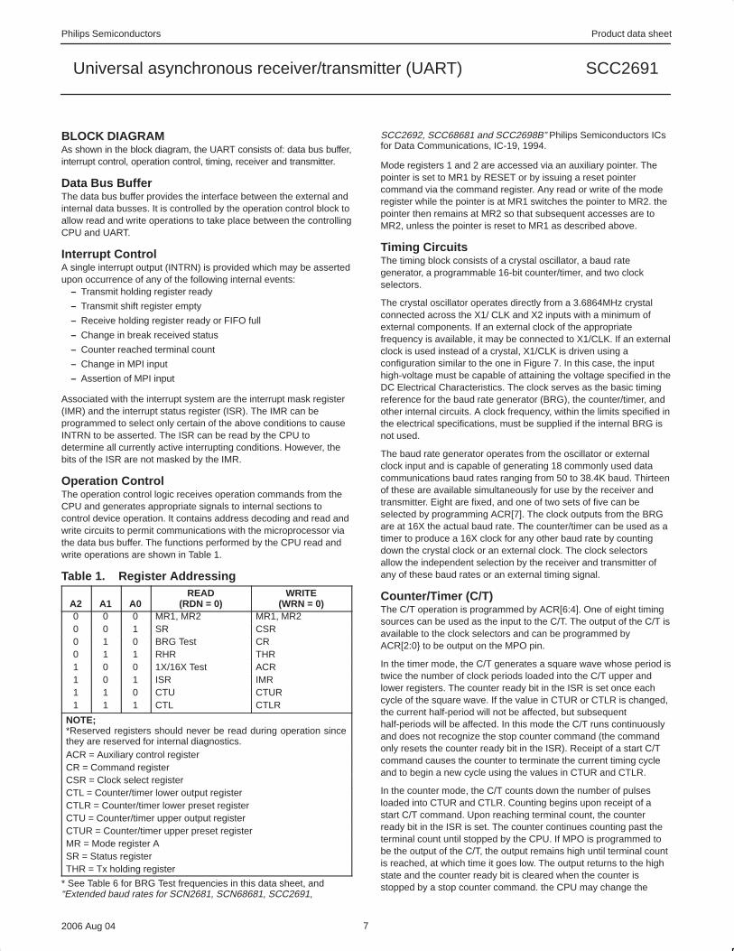
BLOCK DIAGRAMAs shown in the block diagram, the UART consists of: data bus buffer,interrupt control, operation control, timing, receiver and transmitter.
Data Bus BufferThe data bus buffer provides the interface between the external andinternal data busses. It is controlled by the operation control block toallow read and write operations to take place between the controllingCPU and UART.
Interrupt ControlA single interrupt output (INTRN) is provided which may be assertedupon occurrence of any of the following internal events:
– Transmit holding register ready
– Transmit shift register empty
– Receive holding register ready or FIFO full
– Change in break received status
– Counter reached terminal count
– Change in MPI input
– Assertion of MPI input
Associated with the interrupt system are the interrupt mask register(IMR) and the interrupt status register (ISR). The IMR can beprogrammed to select only certain of the above conditions to causeINTRN to be asserted. The ISR can be read by the CPU todetermine all currently active interrupting conditions. However, thebits of the ISR are not masked by the IMR.
Operation ControlThe operation control logic receives operation commands from theCPU and generates appropriate signals to internal sections tocontrol device operation. It contains address decoding and read andwrite circuits to permit communications with the microprocessor viathe data bus buffer. The functions performed by the CPU read andwrite operations are shown in Table 1.
Table 1. Register Addressing
A2 A1 A0READ
(RDN = 0)WRITE
(WRN = 0)0 0 0 MR1, MR2 MR1, MR20 0 1 SR CSR0 1 0 BRG Test CR0 1 1 RHR THR1 0 0 1X/16X Test ACR1 0 1 ISR IMR1 1 0 CTU CTUR1 1 1 CTL CTLR
NOTE;*Reserved registers should never be read during operation sincethey are reserved for internal diagnostics.ACR = Auxiliary control registerCR = Command registerCSR = Clock select registerCTL = Counter/timer lower output registerCTLR = Counter/timer lower preset registerCTU = Counter/timer upper output registerCTUR = Counter/timer upper preset registerMR = Mode register ASR = Status registerTHR = Tx holding register
* See Table 6 for BRG Test frequencies in this data sheet, and“Extended baud rates for SCN2681, SCN68681, SCC2691,
SCC2692, SCC68681 and SCC2698B” Philips Semiconductors ICsfor Data Communications, IC-19, 1994.
Mode registers 1 and 2 are accessed via an auxiliary pointer. Thepointer is set to MR1 by RESET or by issuing a reset pointercommand via the command register. Any read or write of the moderegister while the pointer is at MR1 switches the pointer to MR2. thepointer then remains at MR2 so that subsequent accesses are toMR2, unless the pointer is reset to MR1 as described above.
Timing CircuitsThe timing block consists of a crystal oscillator, a baud rategenerator, a programmable 16-bit counter/timer, and two clockselectors.
The crystal oscillator operates directly from a 3.6864MHz crystalconnected across the X1/ CLK and X2 inputs with a minimum ofexternal components. If an external clock of the appropriatefrequency is available, it may be connected to X1/CLK. If an externalclock is used instead of a crystal, X1/CLK is driven using aconfiguration similar to the one in Figure 7. In this case, the inputhigh-voltage must be capable of attaining the voltage specified in theDC Electrical Characteristics. The clock serves as the basic timingreference for the baud rate generator (BRG), the counter/timer, andother internal circuits. A clock frequency, within the limits specified inthe electrical specifications, must be supplied if the internal BRG isnot used.
The baud rate generator operates from the oscillator or externalclock input and is capable of generating 18 commonly used datacommunications baud rates ranging from 50 to 38.4K baud. Thirteenof these are available simultaneously for use by the receiver andtransmitter. Eight are fixed, and one of two sets of five can beselected by programming ACR[7]. The clock outputs from the BRGare at 16X the actual baud rate. The counter/timer can be used as atimer to produce a 16X clock for any other baud rate by countingdown the crystal clock or an external clock. The clock selectorsallow the independent selection by the receiver and transmitter ofany of these baud rates or an external timing signal.
Counter/Timer (C/T)The C/T operation is programmed by ACR[6:4]. One of eight timingsources can be used as the input to the C/T. The output of the C/T isavailable to the clock selectors and can be programmed byACR[2:0 to be output on the MPO pin.
In the timer mode, the C/T generates a square wave whose period istwice the number of clock periods loaded into the C/T upper andlower registers. The counter ready bit in the ISR is set once eachcycle of the square wave. If the value in CTUR or CTLR is changed,the current half-period will not be affected, but subsequenthalf-periods will be affected. In this mode the C/T runs continuouslyand does not recognize the stop counter command (the commandonly resets the counter ready bit in the ISR). Receipt of a start C/Tcommand causes the counter to terminate the current timing cycleand to begin a new cycle using the values in CTUR and CTLR.
In the counter mode, the C/T counts down the number of pulsesloaded into CTUR and CTLR. Counting begins upon receipt of astart C/T command. Upon reaching terminal count, the counterready bit in the ISR is set. The counter continues counting past theterminal count until stopped by the CPU. If MPO is programmed tobe the output of the C/T, the output remains high until terminal countis reached, at which time it goes low. The output returns to the highstate and the counter ready bit is cleared when the counter isstopped by a stop counter command. the CPU may change the
Philips Semiconductors Product data sheet
SCC2691Universal asynchronous receiver/transmitter (UART)
2006 Aug 04 8
values of CTUR and CTLR at any time, but the new count becomeseffective only on the next start counter command following a stopcounter command. If new values have not been loaded, the previouscount values are preserved and used for the next count cycle.
In the counter mode, the current value of the upper and lower eightbits of the counter may be read by the CPU. It is recommended thatthe counter be stopped when reading to prevent potential problemswhich may occur if a carry from the lower eight bits to the uppereight bits occurs between the times that both halves of the counterare read. However, a subsequent start counter command causesthe counter to begin a new count cycle using the values in CTURand CTLR. See further description in CTUR/CTLR section.
Receiver and TransmitterThe UART is a full-duplex asynchronous receiver/transmitter. Theoperating frequency for the receiver and transmitter can be selectedindependently from the baud rate generator, the counter/timer, orfrom an external input. Registers associated with thecommunications channel are: the mode registers (MR1 and MR2),the clock select register (CSR), the command register (CR), thestatus register (SR), the transmit holding register (THR), and thereceive holding register (RHR).
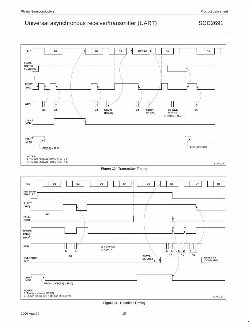
TransmitterThe transmitter accepts parallel data from the CPU and converts itto a serial bit stream on the TxD output pin. It automatically sends astart bit followed by the programmed number of data bits, anoptional parity bit, and the programmed number of stop bits. Theleast significant bit is sent first. Following the transmission of thestop bits, if a new character is not available in the THR, the TxDoutput remains high and the TxEMT bit in the SR will be set to 1.Transmission resumes and the TxEMT bit is cleared when the CPUloads a new character in the THR. In the 16X clock mode, this alsoresynchronizes the internal 1X transmitter clock so that transmissionof the new character begins with minimum delay.
The transmitter can be forced to send a break (continuous lowcondition) by issuing a start break command via the CR. The breakis terminated by a stop break command.
If the transmitter is disabled, it continues operating until thecharacter currently being transmitted and the character in the THR,if any, are completely sent out. Characters cannot be loaded in theTHR while the transmitter is disabled.
ReceiverThe receiver accepts serial data on the RxD pin, converts the serialinput to parallel format, checks for start bit, stop bit, parity bit (if any),or break condition, and presents the assembled character to theCPU. The receiver looks for a high-to-low (mark-to-space) transitionof the start bit on the RxD input pin. If a transition is detected, thestate of the RxD pin is sampled again each 16X clock for 7-1/2clocks (16X clock mode) or at the next rising edge of the bit timeclock (1X clock mode). If RxD is sampled high, the start bit is invalidand the search for a valid start bit begins again. If RxD is still low, avalid start bit is assumed and the receiver continues to sample theinput at one bit time intervals at the theoretical center of the bit, untilthe proper number of data bits and the parity bit (if any) have beenassembled, and one sop bit has been detected. The data is thentransferred to the RHR and the RxRDY bit in the SR is set to a 1. Ifthe character length is less than eight bits, the most significantunused bits in the RHR are set to zero.
After the stop bit is detected, the receiver will immediately look forthe next start bit. However, if a non-zero character was receivedwithout a stop bit (i.e. framing error) and RxD remains low for
one-half of the bit period after the stop bit was sampled, then thereceiver operates as if a new start bit transition had been detected atthat point(one-half bit time after the stop bit was sampled).
The parity error, framing error and overrun error (if any) are strobedinto the SR at the received character boundary, before the RxRDYstatus bit is set.
If a break condition is detected (RxD is low for the entire characterincluding the stop bit), only one character consisting of all zeros willbe loaded in the FIFO and the received SR break bit is set to 1. TheRxD input must return to high for two (2) clock edges of the X1crystal clock for the receiver to recognize the end of the breakcondition and begin the search for a start bit. This will usuallyrequire a high time of one X1 clock period or 3 X1 edges sincethe clock of the controller is not synchronous to the X1 clock.
RECEIVER FIFOThe RHR consists of a first-in-first-out (FIFO) queue with a capacityof three characters. Data is loaded from the receive shift registerinto the top-most empty position of the FIFO. The RxRDY bit in thestatus register (SR) is set whenever one or more characters areavailable to be read, and a FFULL status bit is set if all three queuepositions are filled with data. Either of these bits can be selected tocause an interrupt. A read of the RHR outputs the data at the top ofthe FIFO. After the read cycle, the data FIFO and its associatedstatus bits are ‘popped’ thus emptying a FIFO position for new data.
Receiver Status BitsIn addition to the data word, three status bits (parity error, framingerror, and received break) are appended to each data character inthe FIFO. Status can be provided in two ways, as programmed bythe error mode control bit in mode register 1. In the character mode,status is provided on a character-by-character basis: the statusapplies only to the character at the top of the FIFO. In the blockmode, the status provided in the SR for these three bits is thelogical-OR of the status for all characters coming to the top of theFIFO since the last reset error command was issued. In eithermode, reading the SR does not affect the FIFO. The FIFO is‘popped’ only when the RHR is read. Therefore, the SR should beread prior to reading the corresponding data character.
The receiver can control the deactivation of RTS. If programmed tooperate in this mode, the RTSN output will be negated when a validstart bit was received and the FIFO is full. When a FIFO positionbecomes available, the RTSN output will be re-assertedautomatically. This feature can be used to prevent an overrun, inthe receiver, by connecting the RTSN output to the CTSN input ofthe transmitting device.
Receiver Reset and DisableReceiver disable stops the receiver immediately – data beingassembled if the receiver shift register is lost. Data and status in theFIFO is preserved and may be read. A re-enable of the receiverafter a disable will cause the receiver to begin assemblingcharacters at the next start bit detected. A receiver reset will discardthe present shift register data, reset the receiver ready bit (RxRDY),clear the status of the byte at the top of the FIFO and re-align theFIFO read/write pointers. This has the appearance of “clearing orflushing” the receiver FIFO. In fact, the FIFO is NEVER cleared!The data in the FIFO remains valid until overwritten by anotherreceived character. Because of this, erroneous reading or extrareads of the receiver FIFO will miss-align the FIFO pointers andresult in the reading of previously read data. A receiver reset willre-align the pointers.
Philips Semiconductors Product data sheet
SCC2691Universal asynchronous receiver/transmitter (UART)
2006 Aug 04 9
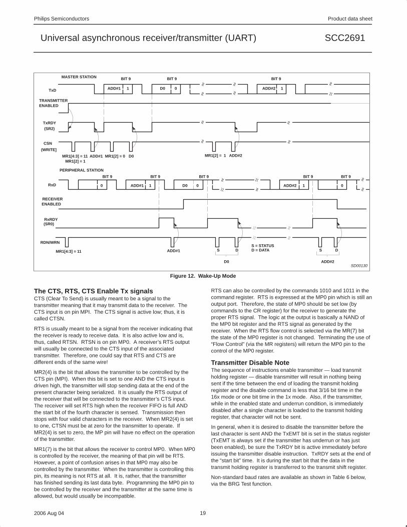
In addition to the normal transmitter and receiver operationdescribed above, the UART incorporates a special mode whichprovides automatic wake-up of the receiver through address framerecognition for multi-processor communications. This mode isselected by programming bits MR1[4:3] to ‘11’.
In this mode of operation, a ‘master’ station transmits an addresscharacter followed by data characters for the addressed ‘slave’station. The slave stations, whose receivers are normally disabled,examine the received data stream and ‘wake-up’ the CPU [bysetting RxRDY) only upon receipt of an address character. The CPUcompares the received address to its station address and enablesthe receiver if it wishes to receive the subsequent data characters.Upon receipt of another address character, the CPU may disable thereceiver to initiate the process again.
A transmitted character consists of a start bit, the programmednumber of data bits, an address/data (A/D) bit, and the programmednumber of stop bits. The polarity of the transmitted A/D bit isselected by the CPU by programming bit MR1[2]. MR1[2] = 0transmits a zero in the A/D bit position which identifies thecorresponding data bits as data, while MR1[2] = 1 transmits a one inthe A/D bit position which identifies the corresponding data bits asan address. The CPU should program the mode register prior toloading the corresponding data bits in the THR.
While in this mode, the receiver continuously looks at the receiveddata stream, whether it is enabled or disabled. If disabled, it sets theRxRDY status bit and loads the character in the RHR FIFO if thereceived A/D bit is a one, but discards the received character if thereceived A/D bit is a zero. If enabled, all received characters arethen transferred to the CPU via the RHR. In either case, the databits are loaded in the data FIFO while the A/D bit is loaded in thestatus FIFO position normally used for parity error (SR[5]). Framingerror, overrun error, and break detect operate normally whether ornot the receiver is enabled.
MULTI-PURPOSE INPUT PINThe MPI pin can be programmed as an input to one of severalUART circuits. The function of the pin is selected by programmingthe appropriate control register (MR2[4]), ACR[6:4], CSR [7:4, 3:0].Only one of the functions may be selected at any given time. If CTSor GPI is selected, a change of state detector provided with the pinis activated. A high-to-low or low-to-high transition of the inputslasting longer than 25–50µs sets the MPI change-of-state bit in theinterrupt status register. The bit is cleared via a command. Thechange-of-state can be programmed to generate an interrupt to theCPU by setting the corresponding bit in the interrupt mask register.
The input port pulse detection circuitry uses a 38.4kHz samplingclock derived from one of the baud rate generator taps. Thisproduces a sampling period of slightly more than 25µs (assuming a3.6864MHz oscillator input). The detection circuitry, in order toguarantee that a true change in level has occurred, requires twosuccessive samples at the new logic level be observed. As aconsequence, the minimum duration of the signal change is 25µs ifthe transition occurs coincident with the first sample pulse. The 50µstime refers to the condition where the change of state is just missedand the first change of state is not detected until after an additional25µs. The MPI pin has a small pull-up device that will source 1 to4 A of current from VCC. This pin does not require pull-up devicesor VCC connection if it is not used.
MULTI-PURPOSE OUTPUT PINThis pin can be programmed to serve as a request-to-send output,the counter/timer output, the output for the 1X or 16X transmitter orreceiver clocks, the TxRDY output or the RxRDY/FFULL output (seeACR[2:0] – MPO Output Select). Please note that this pin drivesboth high and low. HOWEVER when it is programmed to representinterrupt type functions (such as receiver ready, transmitter ready orcounter/timer ready) it will be switched to an open drainconfiguration in which case an external pull-up device would berequired.
REGISTERSThe operation of the UART is programmed by writing control wordsin the appropriate registers. Operational feedback is provided viastatus registers which can be read by the CPU. Addressing of theregisters is as described in Table 1.
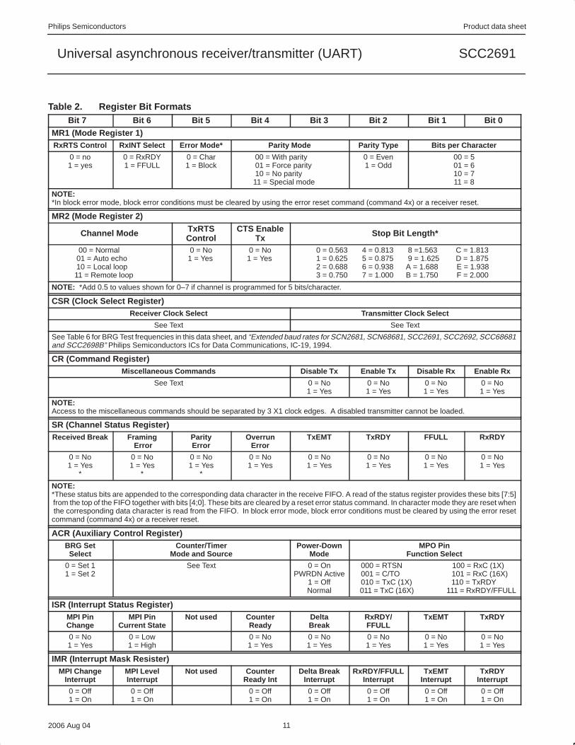
The contents of certain control registers are initialized to zero onreset (see RESET pin description). Care should be exercised if thecontents of a register are changed during operation, since certainchanges may cause operational problems. For example, changingthe number of bits per character while the transmitter is active maycause the transmission of an incorrect character. The contents ofthe MR, the CSR, and the ACR should only be changed while thereceiver and transmitter are disabled, and certain changes to theACR should only be made while the C/T is stopped. The bit formatsof the UART are shown in Table 2.
MR1 – Mode Register 1MR1 is accessed when the MR pointer points to MR1. The pointer isset to MR1 by RESET or by a set pointer command applied via theCR. After reading or writing MR1, the pointers are set at MR2.
MR1[7] – Receiver Request-to-Send ControlThe bit controls the deactivation of the RTSN output (MPO) by thereceiver. This output is normally asserted and negated bycommands applied via the command register. MR1[7] = 1 causesRTSN to be automatically negated upon receipt of a valid start bit ifthe receiver FIFO is full. RTSN is reasserted when an empty FIFOposition is available. This feature can be used to prevent overrun inthe receiver by using the RTSN output signal to control the CTSinput of the transmitting device.
MR1[6] – Receiver Interrupt SelectThis bit selects either the receiver ready status (RxRDY) or the FIFOfull status (FFULL) to be used for CPU interrupts.
MR1[5] – Error Mode SelectThis bit selects the operating mode of the three FIFOed status bits(FE, PE, received break). In the character mode, status is providedon a character-by-character basis. The status applies only to thecharacter at the top of the FIFO. In the block mode, the statusprovided in the SR for these bits is the accumulation (logical-OR) ofthe status for all characters coming to the top of the FIFO since thelast reset error command was issued.
MR1[4:3] – Parity Mode SelectIf with parity or force parity is selected, a parity bit is added to thetransmitted character and the receiver performs a parity check onincoming data. MR![4:3] = 11 selects the channel to operate in thespecial wake-up mode.
MR1[2] – Parity Type SelectThis bit selects the parity type (odd or even) if the with parity modeis programmed by MR1[4:3], and the polarity of the forced parity bitif the force parity mode is programmed. It has no effect if the no
Philips Semiconductors Product data sheet
SCC2691Universal asynchronous receiver/transmitter (UART)
2006 Aug 04 10
parity mode is programmed. In the special wake-up mode, it selectsthe polarity of the transmitted A/D bit.
MR1[1:0] – Bits Per Character SelectThis field selects the number of data bits per character to betransmitted and received. The character length does not include thestart, parity, and stop bits.
MR2 – Mode Register 2MR2 is accessed when the channel MR pointer points to MR2,which occurs after any access to MR1. Accesses to MR2 do notchange the pointer.
MR2[7:6] – Mode SelectThe UART can operate in one of four modes. MR2[7:6] = 00 is thenormal mode, with the transmitter and receiver operatingindependently. MR2[7:6] = 01 places the channel in the automaticecho mode, which automatically re-transmits the received data. Thefollowing conditions are true while in automatic echo mode:1. Received data is re-clocked and retransmitted on the TxD
output.2. The receive clock is used for the transmitter.3. The receiver must be enabled, but the transmitter need not be
enabled.4. The TxRDY and TxEMT status bits are inactive.5. The received parity is checked, but is not regenerated for
transmission, i.e., transmitted parity bit is as received.6. Character framing is checked, but the stop bits are retransmitted
as received.7. A received break is echoed as received until the next valid start
bit is detected.8. CPU-to-receiver communication continues normally, but the
CPU-to-transmitter link is disabled.
Two diagnostic modes can also be selected. MR2[7:6] = 10 selectslocal loopback mode. In this mode:1. The transmitter output is internally connected to the receiver
input.2. The transmit clock is used for the receiver.3. The TxD output is held high.4. The RxD input is ignored.5. The transmitter must be enabled, but the receiver need not be
enabled.6. CPU to transmitter and receiver communications continue
normally.
The second diagnostic mode is the remote loopback mode, selectedby MR2[7:6] = 11. In this mode:1. Received data is re-clocked and retransmitted on the TxD
output.2. The receive clock is used for the transmitter.3. Received data is not sent to the local CPU, and the error status
conditions are inactive.4. The received parity is not checked and is not regenerated for
transmission, i.e., the transmitted parity bit is as received.5. The receiver must be enabled, but the transmitter need not be
enabled.6. Character framing is not checked, and the stop bits are
retransmitted as received.7. A received break is echoed as received until the next valid start
bit is detected.
When switching in and out of the various modes, the selected modeis activated immediately upon mode selection, even if this occurs inthe middle of a received or transmitted character. Likewise, if amode is deselected, the device will switch out of the mode
immediately. An exception to this is switching out of auto-echo orremote loopback modes; if the deselection occurs just after thereceiver has sampled the stop bit (indicated in auto-echo byassertion o fRxRDY), and the transmitter is enabled, the transmitteris enabled, the transmitter will remain in auto-echo mode until onefull stop bit has been retransmitted.
MR2[5] – Transmitter Request-to–Send ControlCAUTION: When the transmitter controls the OP pin (usually usedfor the RTSN signal) the meaning of the pin is not RTSN at all!Rather, it signals that the transmitter has finished the transmission(i.e., end of block).
This bit allows deactivation of the RTSN output by the transmitter.This output is manually asserted and negated by the appropriatecommands issued via the command register. MR2[5] set to 1caused the RTSN to be reset automatically one bit time after thecharacter(s) in the transmit shift register and in the THR (if any) arecompletely transmitted (including the programmed number of stopbits) if a previously issued transmitter disable is pending. Thisfeature can be used to automatically terminate the transmission asfollows:1. Program the auto-reset mode: MR2[5]=12. Enable transmitter, if not already enabled3. Assert RTSN via command4. Send message5. After the last character of the message is loaded to the THR,
disable the transmitter. (If the transmitter is underrun, a specialcase exists. See note below.)
6. The last character will be transmitted and the RTSN will be resetone bit time after the last stop bit is sent.
NOTE: The transmitter is in an underrun condition when both theTxRDY and the TxEMT bits are set. This condition also existsimmediately after the transmitter is enabled from the disabled orreset state. When using the above procedure with the transmitter inthe underrun condition, the issuing of the transmitter disable must bedelayed from the loading of a single, or last, character until theTxRDY becomes active again after the character is loaded.
MR2[4] – Clear-to-Send ControlThe sate of this bit determines if the CTSN input (MPI) controls theoperation of the transmitter. If this bit is 0, CTSN has no effect on thetransmitter. If this bit is a 1, the transmitter checks the sate of CTSNeach time it is ready to send a character. If it is asserted (low), thecharacter is transmitted. If it is negated (high), the TxD outputremains in the marking state and the transmission is delayed untilCTSN goes low. Changes in CTSN while a character is beingtransmitted do not affect the transmission of that character. Thisfeature can be used to prevent overrun of a remote receiver.
MR2[3:0] – Stop Bit Length SelectThis field programs the length of the stop bit appended to thetransmitted character. Stop bit lengths of 9/16 to 1 and 1–9/16 to 2bits, in increments of 1/16 bit, can be programmed for characterlengths of 6, 7, and 8 bits. For a character length of 5 bits, 1–1/16 to2 stop bits can be programmed in increments of 1/16 bit. In allcases, the receiver only checks for a mark condition at the center ofthe first stop bit position (one bit time after the last data bit, or afterthe parity bit if parity is enabled). If an external 1X clock is used forthe transmitter, MR2[3] = 0 selects one stop bit and MR2[3] = 1selects two stop bits to be transmitted.
Philips Semiconductors Product data sheet
SCC2691Universal asynchronous receiver/transmitter (UART)
2006 Aug 04 11
Table 2. Register Bit Formats Bit 7 Bit 6 Bit 5 Bit 4 Bit 3 Bit 2 Bit 1 Bit 0
MR1 (Mode Register 1)RxRTS Control RxINT Select Error Mode* Parity Mode Parity Type Bits per Character
0 = no1 = yes
0 = RxRDY1 = FFULL
0 = Char1 = Block
00 = With parity 01 = Force parity 10 = No parity 11 = Special mode
0 = Even1 = Odd
00 = 501 = 610 = 711 = 8
NOTE:*In block error mode, block error conditions must be cleared by using the error reset command (command 4x) or a receiver reset.
MR2 (Mode Register 2)
Channel Mode TxRTSControl
CTS EnableTx Stop Bit Length*
00 = Normal 01 = Auto echo 10 = Local loop 11 = Remote loop
0 = No 1 = Yes
0 = No 1 = Yes
0 = 0.563 4 = 0.813 8 =1.563 C = 1.813 1 = 0.625 5 = 0.875 9 = 1.625 D = 1.875 2 = 0.688 6 = 0.938 A = 1.688 E = 1.938 3 = 0.750 7 = 1.000 B = 1.750 F = 2.000
NOTE: *Add 0.5 to values shown for 0–7 if channel is programmed for 5 bits/character.
CSR (Clock Select Register)Receiver Clock Select Transmitter Clock Select
See Text See Text
See Table 6 for BRG Test frequencies in this data sheet, and “Extended baud rates for SCN2681, SCN68681, SCC2691, SCC2692, SCC68681and SCC2698B” Philips Semiconductors ICs for Data Communications, IC-19, 1994.
CR (Command Register)Miscellaneous Commands Disable Tx Enable Tx Disable Rx Enable Rx
See Text 0 = No1 = Yes
0 = No1 = Yes
0 = No1 = Yes
0 = No1 = Yes
NOTE:Access to the miscellaneous commands should be separated by 3 X1 clock edges. A disabled transmitter cannot be loaded.
SR (Channel Status Register)Received Break Framing
ErrorParityError
OverrunError
TxEMT TxRDY FFULL RxRDY
0 = No1 = Yes
*
0 = No1 = Yes
*
0 = No1 = Yes
*
0 = No1 = Yes
0 = No1 = Yes
0 = No1 = Yes
0 = No1 = Yes
0 = No1 = Yes
NOTE:*These status bits are appended to the corresponding data character in the receive FIFO. A read of the status register provides these bits [7:5] from the top of the FIFO together with bits [4;0]. These bits are cleared by a reset error status command. In character mode they are reset when the corresponding data character is read from the FIFO. In block error mode, block error conditions must be cleared by using the error resetcommand (command 4x) or a receiver reset.
ACR (Auxiliary Control Register)BRG Set
SelectCounter/Timer
Mode and SourcePower-Down
ModeMPO Pin
Function Select
0 = Set 11 = Set 2
See Text 0 = OnPWRDN Active
1 = OffNormal
000 = RTSN 100 = RxC (1X) 001 = C/TO 101 = RxC (16X) 010 = TxC (1X) 110 = TxRDY 011 = TxC (16X) 111 = RxRDY/FFULL
ISR (Interrupt Status Register)MPI PinChange
MPI PinCurrent State
Not used CounterReady
DeltaBreak
RxRDY/FFULL
TxEMT TxRDY
0 = No1 = Yes
0 = Low1 = High
0 = No1 = Yes
0 = No1 = Yes
0 = No1 = Yes
0 = No1 = Yes
0 = No1 = Yes
IMR (Interrupt Mask Resister)MPI Change
InterruptMPI LevelInterrupt
Not used CounterReady Int
Delta BreakInterrupt
RxRDY/FFULLInterrupt
TxEMTInterrupt
TxRDYInterrupt
0 = Off1 = On
0 = Off1 = On
0 = Off1 = On
0 = Off1 = On
0 = Off1 = On
0 = Off1 = On
0 = Off1 = On
Philips Semiconductors Product data sheet
SCC2691Universal asynchronous receiver/transmitter (UART)
2006 Aug 04 12
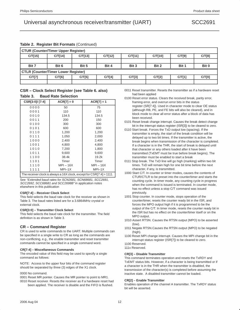
Table 2. Register Bit Formats (Continued)
CTUR (Counter/Timer Upper Register)C/T[15] C/T[14] C/T[13] C/T[12] C/T[11] C/T[10] C/T[9] C/T[8]
Bit 7 Bit 6 Bit 5 Bit 4 Bit 3 Bit 2 Bit 1 Bit 0
CTLR (Counter/Timer Lower Register)C/T[7] C/T[6] C/T[5] C/T[4] C/T[3] C/T[2] C/T[1] C/T[0]
CSR – Clock Select Register (see Table 6. also)Table 3. Baud Rate Selection
CSR[3:0]/ [7:4] ACR[7] = 0 ACR[7] = 1
0 0 0 0 50 750 0 0 1 110 1100 0 1 0 134.5 134.50 0 1 1 200 1500 1 0 0 300 3000 1 0 1 600 6000 1 1 0 1,200 1,2000 1 1 1 1,050 2,0001 0 0 0 2,400 2,4001 0 0 1 4,800 4,8001 0 1 0 7,200 1,8001 0 1 1 9,600 9,6001 1 0 0 38.4k 19.2k1 1 0 1 Timer Timer1 1 1 0 MPI – 16X MPI – 16X1 1 1 1 MPI–1X MPI–1X
The receiver clock is always a 16X clock, except for CSR[7:4] = 1111.
See “Extended baud rates for SCN2681, SCN68681, SCC2691,SCC2692, SCC68681 and SCC2698B” in application noteselsewhere in this publication
CSR[7:4] – Receiver Clock SelectThis field selects the baud rate clock for the receiver as shown inTable 3. The baud rates listed are for a 3.6864MHz crystal orexternal clock.
CSR[3:0] – Transmitter Clock SelectThis field selects the baud rate clock for the transmitter. The fielddefinition is as shown in Table 3.
CR – Command RegisterCR is used to write commands to the UART. Multiple commands canbe specified in a single write to CR as long as the commands arenon-conflicting, e.g., the enable transmitter and reset transmittercommands cannot be specified in a single command word.
CR[7:4] – Miscellaneous CommandsThe encoded value of this field may be used to specify a singlecommand as follows:
NOTE: Access to the upper four bits of the command registershould be separated by three (3) edges of the X1 clock.
0000 No command.0001 Reset MR pointer. Causes the MR pointer to point to MR1.0010 Reset receiver. Resets the receiver as if a hardware reset had
been applied. The receiver is disable and the FIFO is flushed.
0011 Reset transmitter. Resets the transmitter as if a hardware resethad been applied
0100 Reset error status. Clears the received break, parity error,framing error, and overrun error bits in the statusregister (SR[7:4]. Used in character mode to clear OE status(although RB, PE, and FE bits will also be cleared), and inblock mode to clear all error status after a block of data hasbeen received.
0101 Reset break change interrupt. Causes the break detect changebit in the interrupt status register (ISR[3]) to be cleared to zero.
0110 Start break. Forces the TxD output low (spacing). If thetransmitter is empty, the start of the break condition will bedelayed up to two bit times. If the transmitter is active, thebreak begins when transmission of the character is completed.If a character is in the THR, the start of break is delayed untilthat character or any others loaded after it have beentransmitted (TxEMT must be true before break begins). Thetransmitter must be enabled to start a break
0111 Stop break. The TxD line will go high (marking) within two bittimes. TxD will remain high for one bit time before the nextcharacter, if any, is transmitted.
1000 Start C/T. In counter or timer modes, causes the contents ofCTUR/CTLR to be preset into the counter/timer and starts thecounting cycle. In timer mode, any counting cycle in progresswhen the command is issued is terminated. In counter mode,has no effect unless a stop C/T command was issuedpreviously.
1001 Stop counter. In counter mode, stops operation of thecounter/timer, resets the counter ready bit in the ISR, andforces the MPO output high if it is programmed to be theoutput of the C/T. In timer mode, resets the counter ready bit inthe ISR but has no effect on the counter/timer itself or on theMPO output.
1010 Assert RTSN. Causes the RTSN output (MPO) to be asserted(low).
1011 Negate RTSN.Causes the RTSN output (MPO) to be negated(high).
1100 Reset MPI change interrupt. Causes the MPI change bit in theinterrupt status register (ISR[7]) to be cleared to zero.
1100 Reserved.111x Reserved.
CR[3] – Disable TransmitterThis command terminates operation and resets the TxRDY andTxEMT status bits. However, if a character is being transmitted or ifa character is in the THR when the transmitter is disabled, thetransmission of the character(s) is completed before assuming theinactive state. A disabled transmitter cannot be loaded.
CR[2] – Enable TransmitterEnables operation of the channel A transmitter. The TxRDY statusbit will be asserted.
Philips Semiconductors Product data sheet
SCC2691Universal asynchronous receiver/transmitter (UART)
2006 Aug 04 13
CR[1] – Disable ReceiverThis command terminates operation of the receiver immediately; acharacter being received will be lost. The command has no effect onthe receiver status bits or any other control registers. If the specialwake-up mode is programmed, the receiver operates even if it isdisabled (see Wake-up Mode).
CR[0] – Enable ReceiverEnables operation of the receiver. If not in the special wake-upmode, this also forces the receiver into the search for start bit state.
SR – Channel Status RegisterThe status register is updated while RDN is negated. Therefore, thebus interface used with this device must not use a static RDN line.The RDN line must be pulsed to allow status register updates.
SR[7] – Received BreakThis bit indicates that an all zero character of the programmedlength has been received without a stop bit. Only a single FIFOposition is occupied when a break is received; further entries to theFIFO are inhibited until the RxD line returns to the marking state forat least one half bit time two successive edges of the internal orexternal 1X clock. This will usually require a high time of one X1clock period or 3 X1 edges since the clock of the controller isnot synchronous to the X1 clock.
When this bit is set, the change in break bit in the ISR (ISR[3]) isset. ISR[3] is also set when the end of the break condition, asdefined above, is detected.
The break detect circuitry is capable of detecting breaks thatoriginate in the middle of a received character. However, if a breakbegins in the middle of a character, it must last until the end of thenext character time in order for it to be detected.
SR[6] – Framing Error (FE)This bit, when set, indicates that a stop bit was not detected whenthe corresponding data character in the FIFO was received. Thestop bit check is made in the middle of the first stop bit position.
SR[5]– Parity Error (PE)This bit is set when the with parity or force parity mode isprogrammed and the corresponding character in the FIFO wasreceived with incorrect parity. In special wake-up mode, the parityerror bit stores the received A/D bit.
SR[4] – Overrun Error (OE)This bit, when set, indicates that one or more characters in thereceived data stream have been lost. It is set upon receipt of a newcharacter when the FIFO is full and a character is already in thereceive shift register waiting for an empty FIFO position. When thisoccurs, the character in the receive shift register (and its breakdetect, parity error and framing error status, if any) is lost. This bit iscleared by a reset error status command.
SR[3] – Transmitter Empty (TxEMT)This bit will be set when the transmitter underruns, i.e., both theTxEMT and TxRDY bits are set. This bit and TxRDY are set whenthe transmitter is first enabled and at any time it is re-enabled aftereither (a) reset, or (b) the transmitter has assumed the disabledstate. It is always set after transmission of the last stop bit of acharacter if no character is in the THR awaiting transmission.
It is reset when the THR is loaded by the CPU, a pendingtransmitter disable is executed, the transmitter is reset, or thetransmitter is disabled while in the underrun condition.
SR[2] – Transmitter Ready (TxRDY)This bit, when set, indicates that the THR is empty and ready to beloaded with a character. This bit is cleared when the THR is loadedby the CPU and is set when the character is transferred to thetransmit shift register. TxRDY is reset when the transmitter isdisabled and is set when the transmitter is first enabled, e.g.,characters loaded in the THR while the transmitter is disabled willnot be transmitted.
SR[1] – FIFO Full (FFULL)This bit is set when a character is transferred from the receive shiftregister to the receive FIFO and the transfer causes the FIFO tobecome full, i.e., all three FIFO positions are occupied. It is resetwhen the CPU reads the FIFO and there is no character in thereceive shift register. If a character is waiting in the receive shiftregister because the FIFO is full, FFULL will be reset by the CPUread and then set by the transfer of the character to the FIFO, whichcauses all three FIFO positions to be occupied.
SR[0] – Receiver Ready (RxRDY)This bit indicates that a character has been received and is waitingin the FIFO to be read by the CPU. It is set when the character istransferred from the receive shift register to the FIFO and resetwhen the CPU reads the RHR, and no more characters are in theFIFO.
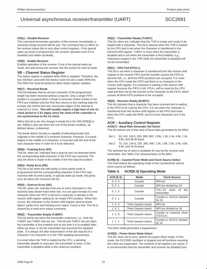
ACR – Auxiliary Control RegisterACR[7] – Baud Rate Generator Set SelectThis bit selects one of two sets of baud rates generated by the BRG.
Set 1: 50, 110, 134.5, 200, 300, 600, 1.05k, 1.2k, 2.4k, 4.8k, 7.2k,9.6k, and 38.4k baud.
Set 2: 75, 110, 134.5, 150, 300, 600, 1.2k, 1.8k, 2.0k, 2.4k, 4.8k,9.6k, and 19.2k baud.
The selected set of rates is available for use by the receiver andtransmitter. See Table 3 for characteristics of the BRG.
ACR[6:4] – Counter/Timer Mode and Clock Source SelectThis field selects the operating mode of the counter/timer and itsclock source as follows:
Table 4. ACR[6:4] Operating Mode
ACR [6:4] Mode Clock Source
0 0 0 Counter MPI pin
0 0 1 Counter MPI pin divided by 16
0 1 0 Counter TxC–1X clock of thetransmitter
0 1 1 Counter Crystal or X1/CLK dividedby 16
1 0 0 Timer (square wave) MPI pin
1 0 1 Timer (square wave) MPI pin divided by 16
1 1 0 Timer (square wave) Crystal or external clock(X1/CLK)
1 1 1 Timer (square wave) Crystal or X1/CLK dividedby 16
The timer mode generates a squarewave.
ACR[3] – Power-Down Mode SelectThis bit, when set to zero, selects the power-down mode. In thismode, the SCC2691 oscillator is stopped and all functions requiringthis clock are suspended. The contents of all registers are saved. Itis recommended that the transmitter and receiver be disabled prior
Philips Semiconductors Product data sheet
SCC2691Universal asynchronous receiver/transmitter (UART)
2006 Aug 04 14
to placing the SCC2691 in this mode. Note that this bit must be setto a logic 1 after reset.
When the power-down mode is enabled, internal circuitry forces theX1/CLK pin to the low state and the X2 pin to the high state. If anexternal clock is being used to drive the device, it is recommendedthat the clock source be three-stated or forced low while the UARTis in power-down mode in order to prevent the clock driver frombeing short circuited.
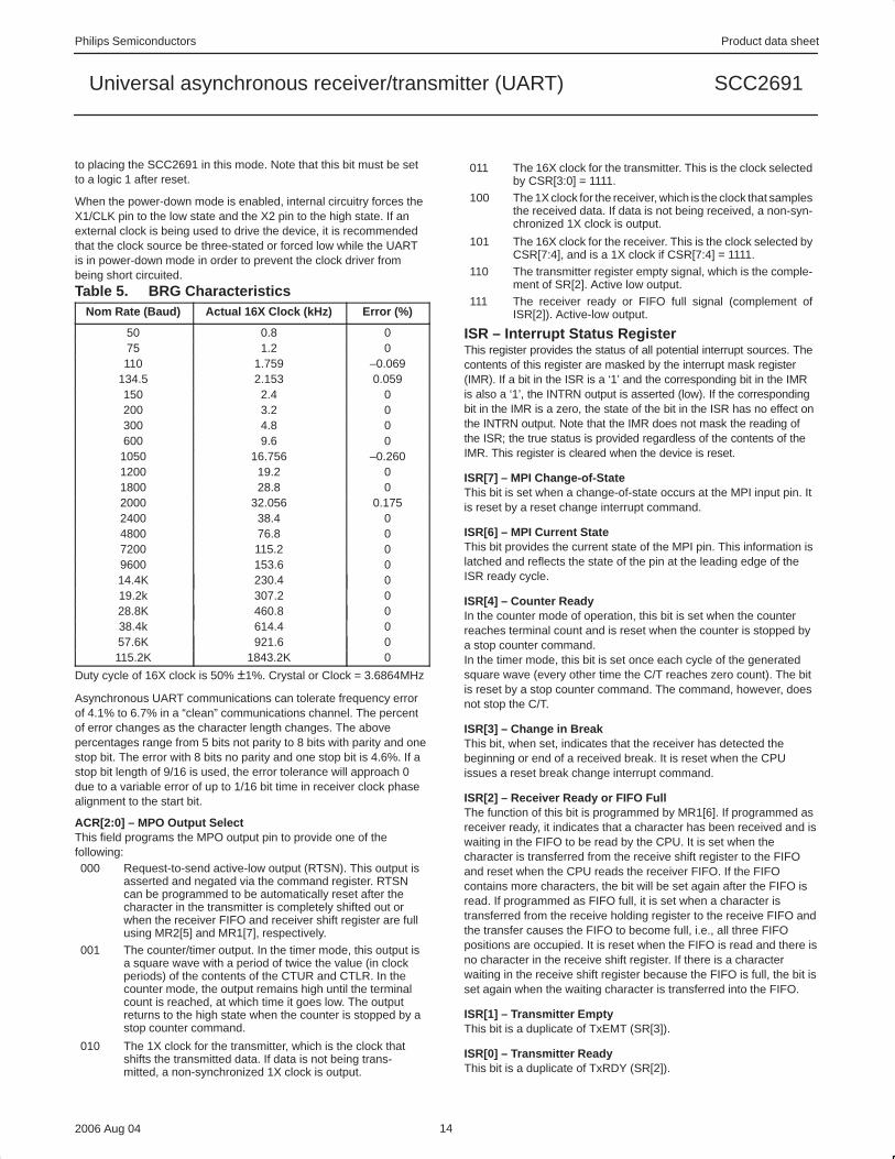
Table 5. BRG CharacteristicsNom Rate (Baud) Actual 16X Clock (kHz) Error (%)
50 0.8 075 1.2 0110 1.759 –0.069
134.5 2.153 0.059150 2.4 0200 3.2 0300 4.8 0600 9.6 01050 16.756 –0.2601200 19.2 01800 28.8 02000 32.056 0.1752400 38.4 04800 76.8 07200 115.2 09600 153.6 014.4K 230.4 019.2k 307.2 028.8K 460.8 038.4k 614.4 057.6K 921.6 0115.2K 1843.2K 0
Duty cycle of 16X clock is 50% ±1%. Crystal or Clock = 3.6864MHz
Asynchronous UART communications can tolerate frequency errorof 4.1% to 6.7% in a “clean” communications channel. The percentof error changes as the character length changes. The abovepercentages range from 5 bits not parity to 8 bits with parity and onestop bit. The error with 8 bits no parity and one stop bit is 4.6%. If astop bit length of 9/16 is used, the error tolerance will approach 0due to a variable error of up to 1/16 bit time in receiver clock phasealignment to the start bit.
ACR[2:0] – MPO Output SelectThis field programs the MPO output pin to provide one of thefollowing:000 Request-to-send active-low output (RTSN). This output is
asserted and negated via the command register. RTSNcan be programmed to be automatically reset after thecharacter in the transmitter is completely shifted out orwhen the receiver FIFO and receiver shift register are fullusing MR2[5] and MR1[7], respectively.
001 The counter/timer output. In the timer mode, this output isa square wave with a period of twice the value (in clockperiods) of the contents of the CTUR and CTLR. In thecounter mode, the output remains high until the terminalcount is reached, at which time it goes low. The outputreturns to the high state when the counter is stopped by astop counter command.
010 The 1X clock for the transmitter, which is the clock thatshifts the transmitted data. If data is not being trans-mitted, a non-synchronized 1X clock is output.
011 The 16X clock for the transmitter. This is the clock selectedby CSR[3:0] = 1111.
100 The 1X clock for the receiver, which is the clock that samplesthe received data. If data is not being received, a non-syn-chronized 1X clock is output.
101 The 16X clock for the receiver. This is the clock selected byCSR[7:4], and is a 1X clock if CSR[7:4] = 1111.
110 The transmitter register empty signal, which is the comple-ment of SR[2]. Active low output.
111 The receiver ready or FIFO full signal (complement ofISR[2]). Active-low output.
ISR – Interrupt Status RegisterThis register provides the status of all potential interrupt sources. Thecontents of this register are masked by the interrupt mask register(IMR). If a bit in the ISR is a ‘1’ and the corresponding bit in the IMRis also a ‘1’, the INTRN output is asserted (low). If the correspondingbit in the IMR is a zero, the state of the bit in the ISR has no effect onthe INTRN output. Note that the IMR does not mask the reading ofthe ISR; the true status is provided regardless of the contents of theIMR. This register is cleared when the device is reset.
ISR[7] – MPI Change-of-StateThis bit is set when a change-of-state occurs at the MPI input pin. Itis reset by a reset change interrupt command.
ISR[6] – MPI Current StateThis bit provides the current state of the MPI pin. This information islatched and reflects the state of the pin at the leading edge of theISR ready cycle.
ISR[4] – Counter ReadyIn the counter mode of operation, this bit is set when the counterreaches terminal count and is reset when the counter is stopped bya stop counter command.In the timer mode, this bit is set once each cycle of the generatedsquare wave (every other time the C/T reaches zero count). The bitis reset by a stop counter command. The command, however, doesnot stop the C/T.
ISR[3] – Change in BreakThis bit, when set, indicates that the receiver has detected thebeginning or end of a received break. It is reset when the CPUissues a reset break change interrupt command.
ISR[2] – Receiver Ready or FIFO FullThe function of this bit is programmed by MR1[6]. If programmed asreceiver ready, it indicates that a character has been received and iswaiting in the FIFO to be read by the CPU. It is set when thecharacter is transferred from the receive shift register to the FIFOand reset when the CPU reads the receiver FIFO. If the FIFOcontains more characters, the bit will be set again after the FIFO isread. If programmed as FIFO full, it is set when a character istransferred from the receive holding register to the receive FIFO andthe transfer causes the FIFO to become full, i.e., all three FIFOpositions are occupied. It is reset when the FIFO is read and there isno character in the receive shift register. If there is a characterwaiting in the receive shift register because the FIFO is full, the bit isset again when the waiting character is transferred into the FIFO.
ISR[1] – Transmitter EmptyThis bit is a duplicate of TxEMT (SR[3]).
ISR[0] – Transmitter ReadyThis bit is a duplicate of TxRDY (SR[2]).
Philips Semiconductors Product data sheet
SCC2691Universal asynchronous receiver/transmitter (UART)
2006 Aug 04 15
IMR – Interrupt Mask RegisterThe programming of this register selects which bits in the ISR cause aninterrupt output. If a bit in the ISR is a ‘1’ and the corresponding bit inthe IMR is a ‘1’, the INTRN output is asserted (low). If the correspondingbit in the IMR is a zero, the state of the bit in the ISR has no effect onthe INTRN output. Note that the IMR does not mask reading of the ISR.NOTE: When IMR[6] is a 1, a 1 on the MPI pin causes and interrupt.
CTUR and CTLR – Counter/Timer RegistersThe CTUR and CTLR hold the eight MSBs and eight LSBs,respectively, of the value to be used by the counter/timer in eitherthe counter or timer modes of operation. The minimum value whichmay be loaded is H‘0002’.
In the timer (programmable divider) mode, the C/T generates asquare wave whose period is twice the value (in clock periods) ofthe CTUR and CTLR. The waveform so generated is often used fora data clock. The formula for calculating the divisor n to load to theCTUR and CTLR for a particular 1X data clock is shown below:
n CT Clock Frequency
2 x 16 x Baud rate desired
Often this division will result in a non-integer number; 26.3, forexample. One can only program integer numbers in a digital divider.Therefore, 26 would be chosen. This gives a baud rate error of
0.3/26.3 which is 1.14%; well within the ability asynchronous modeof operation.
If the value in CTUR or CTLR is changed, the current half-period willnot be affected, but subsequent half-periods will be.
The counter ready status bit (ISR[4]) is set once each cycle of thesquare wave. The bit is reset by a stop counter command. Thecommand, however, does not stop the C/T. The generated squarewave is output on MPO if it is programmed to be the C/T output.
In the counter mode, the C/T counts down the number of pulsesloaded in CTUR and CTLR. Counting begins upon receipt of a startC/T command. Upon reaching the terminal count, the counter readyinterrupt bit (ISR[4]) is set. the counter continues counting past theterminal count until stopped by the CPU. If MPO is programmed tobe the output of the C/T, the output remains high until the terminalcount is reached, at which time it goes low.
The output returns to the high state and ISR[4] is cleared when thecounter is stopped by a stop counter command. The CPU maychange the values of CTUR and CTLR at any time, but the newcount becomes effective only on the next start counter command. Ifnew values have not been loaded, the previous values arepreserved and used for the next count cycle.
SD00028
RESET
tRES
Figure 3. Reset Timing
A0–A2
CEN
RDN
D0–D7(READ)
WRN
D0–D7(WRITE)
tAS
tAH
tCStRWD
tDD tDF
tRWD
tDHtDS
tRW
tCH
FLOAT FLOATNOT VALID VALID
VALID
SD00124
Figure 4. Bus Timing
Philips Semiconductors Product data sheet
SCC2691Universal asynchronous receiver/transmitter (UART)
2006 Aug 04 16
RDN
MPI
WRN
MPO
tPS tPH
tPD
SD00125
Figure 5. I/O Timing
WRN
INTERRUPT1
OUTPUT
RDN
INTERRUPT1
OUTPUT
VM
tIR
tIR
VOL +0.5V
VOL +0.5V
VOL
VOL
NOTES:1. INTRN or MPO when used as interrupt outputs.2. The test for open drain outputs is intended to guarantee switching of the output transistor. Measurement of this response is referenced from the midpoint of the switching signal,
VM, to a point 0.5V above VOL. This point represents noise margin that assures true switching has occurred. Beyond this level, the effects of external circuitry and test environmentare pronounced and can greatly affect the resultant measurement.
SD00126
Figure 6. Interrupt Timing
X1/CLKC/T CLK
RxCTxC
tCLKtCTCtRxtTx
tCLKtCTCtRxtTx
C1
C2
Y1
X1/CLK
X2
SCC2691
Y1 = 3.6864MHz, CL = 20pF
C1 = C2 = 24pF
CLK 5V
470Ω
X1
X2N/C
TYPICAL CRYSTAL SPECIFICATION
FREQUENCY. . . . . . . . . . . . . . 2–4MHzLOAD CAPACITANCE (C L). . . 20 or 32pF (typical)
TYPE OF OPERATION . . . . . .PARALLEL RESONANT, FUND. MODE
DRIVINGFROM EXTERNAL
SOURCE
50kto150k
SD00127
Figure 7. Clock Timing
Philips Semiconductors Product data sheet
SCC2691Universal asynchronous receiver/transmitter (UART)
2006 Aug 04 17
tTXD
tTCS
1 BIT TIME(1 OR 16 CLOCKS)
TxD
TxC(INPUT)
TxC(1X OUTPUT)
SD00092
Figure 8. Transmit Timing
tRXS tRXH
RxC(1X INPUT)
RxD
SD00093
Figure 9. Receive Timing
Philips Semiconductors Product data sheet
SCC2691Universal asynchronous receiver/transmitter (UART)
2006 Aug 04 18
TxD D1 D2 D3 BREAK D4 D6
TRANS-MITTERENABLED
TxRDY(SR2)
WRN
CTSN1(MPI)
(MPO)RTSN2
D1 D2 D3 STARTBREAK
D4 STOPBREAK
D5 WILLNOT BE
TRANSMITTED
D6
CR[7:4] = 1010 CR[7:4] = 1010
NOTES:1. TIMING SHOWN FOR MR2[4] = 1.2. TIMING SHOWN FOR MR2[5] = 1.
SD00128
Figure 10. Transmitter Timing
D1 D2 D4 D5 D6 D7 D8D3RxD
RECEIVERENABLED
RxRDY(SR0)
FFULL(SR1)
RxRDY/
RDN
OVERRRUN(SR4)
RTS1MPO
NOTES;1. Timing shown for MR1[7].2. Shown for ACR[2:] = 111 and MR1[6] = 0.
FFULLMPO2
MPO = 1 (CR[7:4] = 1010)
RESET BY COMMAND
D5 WILLBE LOST
S D S D S D S D
D2 D3 D4D1
S = STATUSD = DATA
D2
SD00129
Figure 11. Receiver Timing
Philips Semiconductors Product data sheet
SCC2691Universal asynchronous receiver/transmitter (UART)
2006 Aug 04 19
MASTER STATION
TxD
TRANSMITTERENABLED
TxRDY(SR2)
CSN
(WRITE]
PERIPHERAL STATION
RxD
RECEIVERENABLED
RxRDY(SR0)
RDN/WRN
ADD#1 1 D0 0 ADD#2 1
BIT 9 BIT 9 BIT 9
BIT 9 BIT 9 BIT 9 BIT 9 BIT 9
MR1[4:3] = 11MR1[2] = 1
ADD#1 MR1[2] = 0 D0 MR1[2] = 1 ADD#2
0 ADD#1 1 D0 0 ADD#2 1 0
MR1[4:3] = 11 ADD#1
D0
S DS = STATUSD = DATA S D
ADD#2SD00130
Figure 12. Wake-Up Mode
The CTS, RTS, CTS Enable Tx signalsCTS (Clear To Send) is usually meant to be a signal to thetransmitter meaning that it may transmit data to the receiver. TheCTS input is on pin MPI. The CTS signal is active low; thus, it iscalled CTSN.
RTS is usually meant to be a signal from the receiver indicating thatthe receiver is ready to receive data. It is also active low and is,thus, called RTSN. RTSN is on pin MP0. A receiver’s RTS outputwill usually be connected to the CTS input of the associatedtransmitter. Therefore, one could say that RTS and CTS aredifferent ends of the same wire!
MR2(4) is the bit that allows the transmitter to be controlled by theCTS pin (MPI). When this bit is set to one AND the CTS input isdriven high, the transmitter will stop sending data at the end of thepresent character being serialized. It is usually the RTS output ofthe receiver that will be connected to the transmitter’s CTS input.The receiver will set RTS high when the receiver FIFO is full ANDthe start bit of the fourth character is sensed. Transmission thenstops with four valid characters in the receiver. When MR2(4) is setto one, CTSN must be at zero for the transmitter to operate. IfMR2(4) is set to zero, the MP pin will have no effect on the operationof the transmitter.
MR1(7) is the bit that allows the receiver to control MP0. When MP0is controlled by the receiver, the meaning of that pin will be RTS.However, a point of confusion arises in that MP0 may also becontrolled by the transmitter. When the transmitter is controlling thispin, its meaning is not RTS at all. It is, rather, that the transmitterhas finished sending its last data byte. Programming the MP0 pin tobe controlled by the receiver and the transmitter at the same time isallowed, but would usually be incompatible.
RTS can also be controlled by the commands 1010 and 1011 in thecommand register. RTS is expressed at the MP0 pin which is still anoutput port. Therefore, the state of MP0 should be set low (bycommands to the CR register) for the receiver to generate theproper RTS signal. The logic at the output is basically a NAND ofthe MP0 bit register and the RTS signal as generated by thereceiver. When the RTS flow control is selected via the MR(7) bitthe state of the MP0 register is not changed. Terminating the use of“Flow Control” (via the MR registers) will return the MP0 pin to thecontrol of the MP0 register.
Transmitter Disable NoteThe sequence of instructions enable transmitter — load transmitholding register — disable transmitter will result in nothing beingsent if the time between the end of loading the transmit holdingregister and the disable command is less that 3/16 bit time in the16x mode or one bit time in the 1x mode. Also, if the transmitter,while in the enabled state and underrun condition, is immediatelydisabled after a single character is loaded to the transmit holdingregister, that character will not be sent.
In general, when it is desired to disable the transmitter before thelast character is sent AND the TxEMT bit is set in the status register(TxEMT is always set if the transmitter has underrun or has justbeen enabled), be sure the TxRDY bit is active immediately beforeissuing the transmitter disable instruction. TxRDY sets at the end ofthe “start bit” time. It is during the start bit that the data in thetransmit holding register is transferred to the transmit shift register.
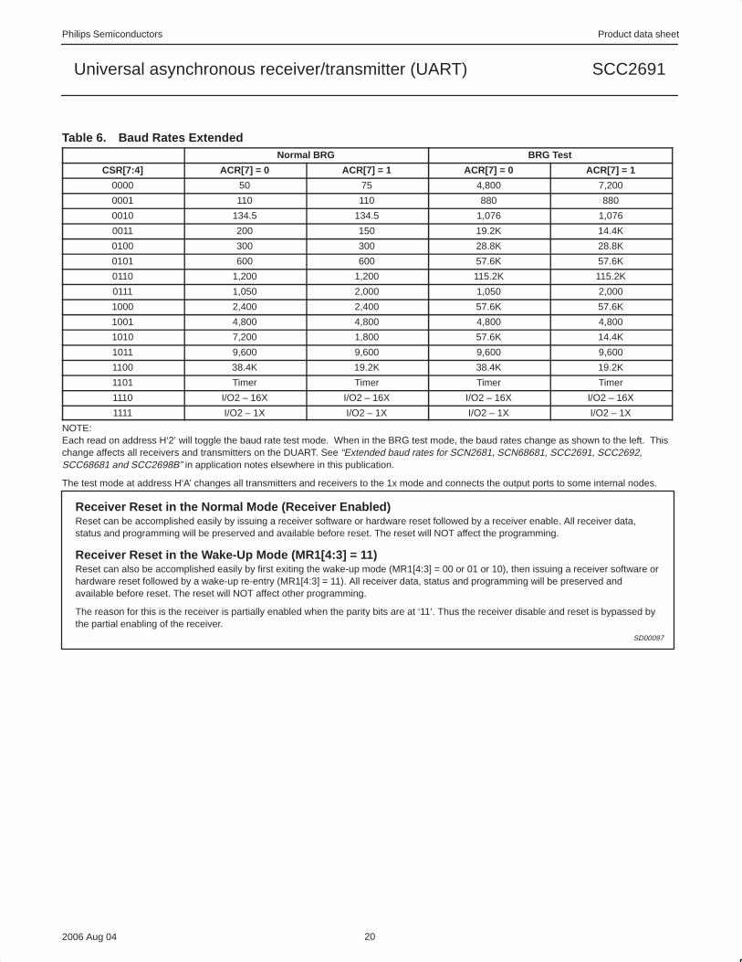
Non-standard baud rates are available as shown in Table 6 below,via the BRG Test function.
Philips Semiconductors Product data sheet
SCC2691Universal asynchronous receiver/transmitter (UART)
2006 Aug 04 20
Table 6. Baud Rates ExtendedNormal BRG BRG Test
CSR[7:4] ACR[7] = 0 ACR[7] = 1 ACR[7] = 0 ACR[7] = 1
0000 50 75 4,800 7,200
0001 110 110 880 880
0010 134.5 134.5 1,076 1,076
0011 200 150 19.2K 14.4K
0100 300 300 28.8K 28.8K
0101 600 600 57.6K 57.6K
0110 1,200 1,200 115.2K 115.2K
0111 1,050 2,000 1,050 2,000
1000 2,400 2,400 57.6K 57.6K
1001 4,800 4,800 4,800 4,800
1010 7,200 1,800 57.6K 14.4K
1011 9,600 9,600 9,600 9,600
1100 38.4K 19.2K 38.4K 19.2K
1101 Timer Timer Timer Timer
1110 I/O2 – 16X I/O2 – 16X I/O2 – 16X I/O2 – 16X
1111 I/O2 – 1X I/O2 – 1X I/O2 – 1X I/O2 – 1X
NOTE:Each read on address H‘2’ will toggle the baud rate test mode. When in the BRG test mode, the baud rates change as shown to the left. Thischange affects all receivers and transmitters on the DUART. See “Extended baud rates for SCN2681, SCN68681, SCC2691, SCC2692,SCC68681 and SCC2698B” in application notes elsewhere in this publication.
The test mode at address H‘A’ changes all transmitters and receivers to the 1x mode and connects the output ports to some internal nodes.
Receiver Reset in the Normal Mode (Receiver Enabled)Reset can be accomplished easily by issuing a receiver software or hardware reset followed by a receiver enable. All receiver data,status and programming will be preserved and available before reset. The reset will NOT affect the programming.
Receiver Reset in the Wake-Up Mode (MR1[4:3] = 11)Reset can also be accomplished easily by first exiting the wake-up mode (MR1[4:3] = 00 or 01 or 10), then issuing a receiver software orhardware reset followed by a wake-up re-entry (MR1[4:3] = 11). All receiver data, status and programming will be preserved andavailable before reset. The reset will NOT affect other programming.
The reason for this is the receiver is partially enabled when the parity bits are at ‘11’. Thus the receiver disable and reset is bypassed bythe partial enabling of the receiver.
SD00097
Philips Semiconductors Product data sheet
SCC2691Universal asynchronous receiver/transmitter (UART)
2006 Aug 04 21
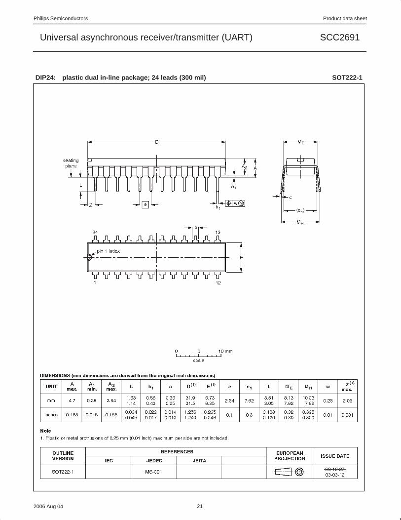
DIP24: plastic dual in-line package; 24 leads (300 mil) SOT222-1
Philips Semiconductors Product data sheet
SCC2691Universal asynchronous receiver/transmitter (UART)
2006 Aug 04 22
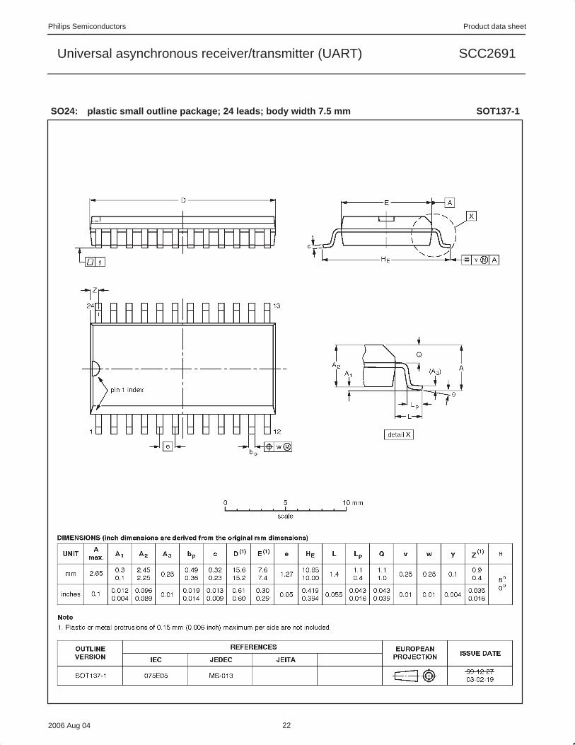
SO24: plastic small outline package; 24 leads; body width 7.5 mm SOT137-1
Philips Semiconductors Product data sheet
SCC2691Universal asynchronous receiver/transmitter (UART)
2006 Aug 04 23
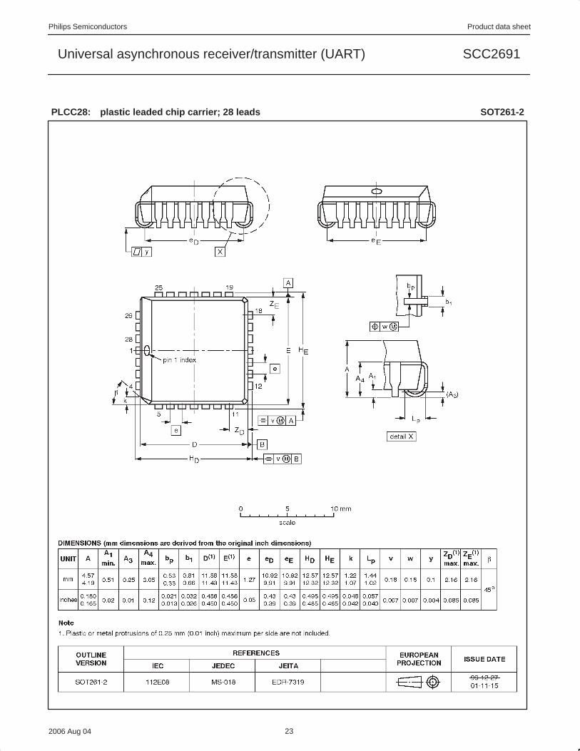
PLCC28: plastic leaded chip carrier; 28 leads SOT261-2
Philips Semiconductors Product data sheet
SCC2691Universal asynchronous receiver/transmitter (UART)
2006 Aug 04 24
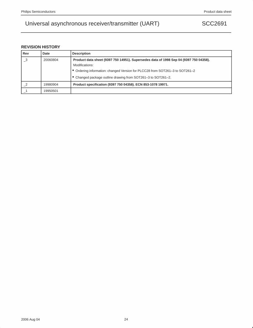
REVISION HISTORY
Rev Date Description
_3 20060804 Product data sheet (9397 750 14951). Supersedes data of 1998 Sep 04 (9397 750 04358).
Modifications:
• Ordering information: changed Version for PLCC28 from SOT261–3 to SOT261–2
• Changed package outline drawing from SOT261–3 to SOT261–2.
_2 19980904 Product specification (9397 750 04358). ECN 853-1078 19971.
_1 19950501
Philips Semiconductors Product data sheet
SCC2691Universal asynchronous receiver/transmitter (UART)
yyyy mmm dd 25
This document contains data from the preliminary specification.
Development
Preliminary [short] data sheet
Data sheet statusDocument status [1][2]
Objective [short] data sheet
Product status [3] Definition
This document contains data from the objective specification for product development.
[1] Please consult the most recently issued document before initiating or completing a design.
[2] The term ‘short data sheet’ is explained in section “Definitions”.
[3] The product status of device(s) described in this document may have changed since this data sheet was published and may differ in case of multiple devices. The latest product statusinformation is available on the Internet at URL http://www.semiconductors.philips.com.
Qualification
Product [short] data sheet Production This document contains the product specification.
DefinitionsDraft — The document is a draft version only. The content is still underinternal review and subject to formal approval, which may result inmodifications or additions. Philips Semiconductors does not give anyrepresentations or warranties as to the accuracy or completeness ofinformation included herein and shall have no liability for the consequencesof use of such information.
Short data sheet — A short data sheet is an extract from a full data sheetwith the same product type number(s) and title. A short data sheet isintended for quick reference only and should not be relied upon to containdetailed and full information. For detailed and full information see therelevant full data sheet, which is available on request via the local PhilipsSemiconductors sales office. In case of any inconsistency or conflict with theshort data sheet, the full data sheet shall prevail.
DisclaimersGeneral — Information in this document is believed to be accurate andreliable. However, Philips Semiconductors does not give any representationsor warranties, expressed or implied, as to the accuracy or completeness ofsuch information and shall have no liability for the consequences of use ofsuch information.
Right to make changes — Philips Semiconductors reserves the right tomake changes to information published in this document, including withoutlimitation specifications and product descriptions, at any time and withoutnotice. This document supersedes and replaces all information supplied priorto the publication hereof.
Suitability for use — Philips Semiconductors products are not designed,authorized or warranted to be suitable for use in medical, military, aircraft,space or life support equipment, nor in applications where failure ormalfunction of a Philips Semiconductors product can reasonably beexpected to result in personal injury, death or severe property or
environmental damage. Philips Semiconductors accepts no liability forinclusion and/or use of Philips Semiconductors products in such equipmentor applications and therefore such inclusion and/or use is at the customer’sown risk.
Applications — Applications that are described herein for any of theseproducts are for illustrative purposes only. Philips Semiconductors makes norepresentation or warranty that such applications will be suitable for thespecified use without further testing or modification.
Limiting values — Stress above one or more limiting values (as defined inthe Absolute Maximum Ratings System of IEC 60134) may causepermanent damage to the device. Limiting values are stress ratings only andoperation of the device at these or any other conditions above those given inthe Characteristics sections of this document is not implied. Exposure tolimiting values for extended periods may affect device reliability.
Terms and conditions of sale — Philips Semiconductors products aresold subject to the general terms and conditions of commercial sale, aspublished at http://www.semiconductors.philips.com/profile/terms ,including those pertaining to warranty, intellectual property rightsinfringement and limitation of liability, unless explicitly otherwise agreed to inwriting by Philips Semiconductors. In case of any inconsistency or conflictbetween information in this document and such terms and conditions, thelatter will prevail.
No offer to sell or license — Nothing in this document may be interpretedor construed as an offer to sell products that is open for acceptance or thegrant, conveyance or implication of any license under any copyrights,patents or other industrial or intellectual property rights.
TrademarksNotice: All referenced brands, product names, service names andtrademarks are the property of their respective owners.
Contact information
For additional information please visit: http://www.semiconductors.philips.com
For sales office addresses, send an e-mail to: [email protected] .
Please be aware that important notices concerning this document and the product(s)described herein, have been included in section ‘Legal information’.
Koninklijke Philips Electronics N.V. 2006. All rights reserved.For more information, please visit http://www.semiconductors.philips.com.For sales office addresses, email to: [email protected].
Date of release: 20060804
Document identifier: SCC2691_3
Legal Information