SCAS283S –JANUARY 1993–REVISED AUGUST 2015 … · SN74LVC08A Quadruple 2-Input Positive-AND...
34
A B Y Y + A • B or Y + A ) B Product Folder Sample & Buy Technical Documents Tools & Software Support & Community SN54LVC08A, SN74LVC08A SCAS283S – JANUARY 1993 – REVISED AUGUST 2015 SN74LVC08A Quadruple 2-Input Positive-AND Gates 1 Features 2 Applications 1• Operate From 1.65 V to 3.6 V • Servers • Specified From –40°C to 85°C, –40°C to 125°C, • LED Displays and –55°C to 125°C • Network Switches • Inputs Accept Voltages to 5.5 V • I/O expanders • Max t pd of 4.1 ns at 3.3 V • Base station processor board • Typical V OLP (Output Ground Bounce) 3 Description <0.8 V at V CC = 3.3 V, T A = 25°C The SN54LVC08A quadruple 2-input positive-AND • Typical V OHV (Output V OH Undershoot) gate is designed for 2.7-V to 3.6-V V CC operation, and >2 V at V CC = 3.3 V, T A = 25°C the SN74LVC08A quadruple 2-input positive-AND • I off Support Live Insertion, Partial-Power-Down gate is designed for 1.65-V to 3.6-V V CC operation. Mode and Back-Drive Protection The LVC08A devices perform the Boolean function • Latch-Up Performance Exceeds 250 mA in positive logic. Per JESD 17 • ESD Protection Exceeds JESD 22 Inputs can be driven from either 3.3-V or 5-V devices. This feature allows the use of these devices as – 2000-V Human-Body Model (A114-A) translators in a mixed 3.3-V/5-V system environment. – 200-V Machine Model (A115-A) – 1000-V Charged-Device Model (C101) Device Information (1) PART NUMBER PACKAGE BODY SIZE (NOM) – On Products Compliant to MIL-PRF-38535, All Parameters Are Tested Unless Otherwise CFP (14) 9.21 mm × 5.97 mm Noted. On All Other Products, Production SNJ54LVC08A CDIP (14) 19.56 mm × 6.92 mm Processing Does Not Necessarily Include LCCC (20) 8.89 mm × 8.89 mm Testing of All Parameters. VQFN (14) 3.50 mm × 3.50 mm TSSOP (14) 5.00 mm × 4.40 mm SN74LVC08A SOP (14) 10.30 mm × 5.30 mm SOIC (14) 8.65 mm × 3.91 mm SSOP (14) 6.20 mm × 5.30 mm (1) For all available packages, see the orderable addendum at the end of the data sheet. Logic Diagram, Each Gate (Positive Logic) 1 An IMPORTANT NOTICE at the end of this data sheet addresses availability, warranty, changes, use in safety-critical applications, intellectual property matters and other important disclaimers. PRODUCTION DATA.
Transcript of SCAS283S –JANUARY 1993–REVISED AUGUST 2015 … · SN74LVC08A Quadruple 2-Input Positive-AND...

A
BY
Y� A • B or Y� A� B
Product
Folder
Sample &Buy
Technical
Documents
Tools &
Software
Support &Community
SN54LVC08A, SN74LVC08ASCAS283S –JANUARY 1993–REVISED AUGUST 2015
SN74LVC08A Quadruple 2-Input Positive-AND Gates1 Features 2 Applications1• Operate From 1.65 V to 3.6 V • Servers• Specified From –40°C to 85°C, –40°C to 125°C, • LED Displays
and –55°C to 125°C • Network Switches• Inputs Accept Voltages to 5.5 V • I/O expanders• Max tpd of 4.1 ns at 3.3 V • Base station processor board• Typical VOLP (Output Ground Bounce)
3 Description<0.8 V at VCC = 3.3 V, TA = 25°CThe SN54LVC08A quadruple 2-input positive-AND• Typical VOHV (Output VOH Undershoot)gate is designed for 2.7-V to 3.6-V VCC operation, and>2 V at VCC = 3.3 V, TA = 25°Cthe SN74LVC08A quadruple 2-input positive-AND• Ioff Support Live Insertion, Partial-Power-Down gate is designed for 1.65-V to 3.6-V VCC operation.Mode and Back-Drive ProtectionThe LVC08A devices perform the Boolean function• Latch-Up Performance Exceeds 250 mA
in positive logic.Per JESD 17• ESD Protection Exceeds JESD 22 Inputs can be driven from either 3.3-V or 5-V devices.
This feature allows the use of these devices as– 2000-V Human-Body Model (A114-A)translators in a mixed 3.3-V/5-V system environment.
– 200-V Machine Model (A115-A)– 1000-V Charged-Device Model (C101) Device Information(1)
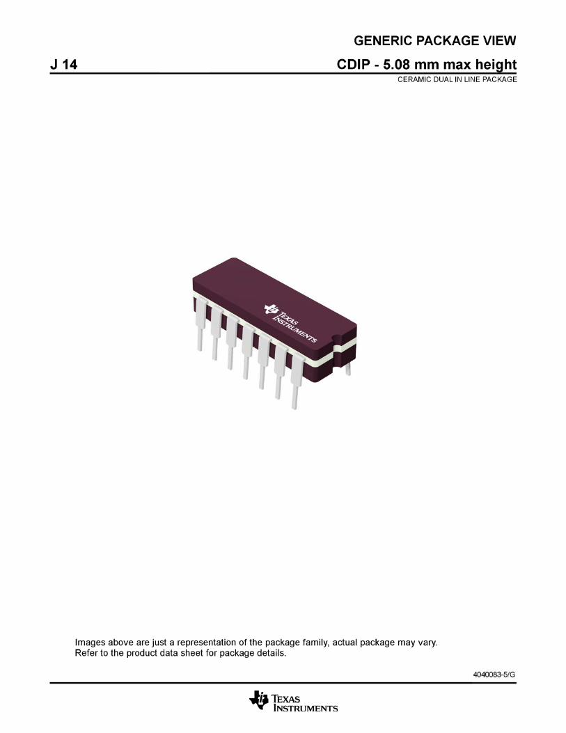
PART NUMBER PACKAGE BODY SIZE (NOM)– On Products Compliant to MIL-PRF-38535,All Parameters Are Tested Unless Otherwise CFP (14) 9.21 mm × 5.97 mmNoted. On All Other Products, Production SNJ54LVC08A CDIP (14) 19.56 mm × 6.92 mmProcessing Does Not Necessarily Include LCCC (20) 8.89 mm × 8.89 mmTesting of All Parameters. VQFN (14) 3.50 mm × 3.50 mm
TSSOP (14) 5.00 mm × 4.40 mmSN74LVC08A SOP (14) 10.30 mm × 5.30 mm
SOIC (14) 8.65 mm × 3.91 mmSSOP (14) 6.20 mm × 5.30 mm
(1) For all available packages, see the orderable addendum atthe end of the data sheet.
Logic Diagram, Each Gate(Positive Logic)
1
An IMPORTANT NOTICE at the end of this data sheet addresses availability, warranty, changes, use in safety-critical applications,intellectual property matters and other important disclaimers. PRODUCTION DATA.

SN54LVC08A, SN74LVC08ASCAS283S –JANUARY 1993–REVISED AUGUST 2015 www.ti.com
Table of Contents1 Features .................................................................. 1 9 Detailed Description ............................................ 10
9.1 Overview ................................................................. 102 Applications ........................................................... 19.2 Functional Block Diagram ....................................... 103 Description ............................................................. 19.3 Feature Description................................................. 104 Revision History..................................................... 29.4 Device Functional Modes........................................ 105 Device Options....................................................... 3
10 Application and Implementation........................ 116 Pin Configuration and Functions ......................... 410.1 Application Information.......................................... 117 Specifications......................................................... 510.2 Typical Application ............................................... 117.1 Absolute Maximum Ratings ..................................... 5
11 Power Supply Recommendations ..................... 127.2 ESD Ratings.............................................................. 512 Layout................................................................... 127.3 Recommended Operating Conditions for
12.1 Layout Guidelines ................................................. 12SN54LVC08A ............................................................ 512.2 Layout Examples................................................... 127.4 Recommended Operating Conditions for
SN74LVC08A ............................................................ 6 13 Device and Documentation Support ................. 137.5 Thermal Information .................................................. 6 13.1 Related Links ........................................................ 137.6 Electrical Characteristics for SN54LVC08A .............. 7 13.2 Community Resources.......................................... 137.7 Electrical Characteristics for SN74LVC08A .............. 7 13.3 Trademarks ........................................................... 137.8 Switching Characteristics for SN54LVC08A ............. 7 13.4 Electrostatic Discharge Caution............................ 137.9 Switching Characteristics for SN74LVC08A ............. 8 13.5 Glossary ................................................................ 137.10 Operating Characteristics........................................ 8 14 Mechanical, Packaging, and Orderable7.11 Typical Characteristics ............................................ 8 Information ........................................................... 13
8 Parameter Measurement Information .................. 9
4 Revision HistoryNOTE: Page numbers for previous revisions may differ from page numbers in the current version.
Changes from Revision R (June 2015) to Revision S Page
• Added TJ junction temperature spec to Abs Max Ratings ..................................................................................................... 5
Changes from Revision Q (November 2010) to Revision R Page
• Updated document to new TI data sheet format - no specification changes. ........................................................................ 1• Added Applications, Device Information table, Pin Configuration and Functions section, ESD Ratings table, Feature
Description section, Device Functional Modes, Application and Implementation section, Power SupplyRecommendations section, Layout section, Device and Documentation Support section, and Mechanical,Packaging, and Orderable Information section ...................................................................................................................... 1
• Added Military Disclaimer to Features.................................................................................................................................... 1• Added Thermal Information table ........................................................................................................................................... 6
2 Submit Documentation Feedback Copyright © 1993–2015, Texas Instruments Incorporated
Product Folder Links: SN54LVC08A SN74LVC08A

SN54LVC08A, SN74LVC08Awww.ti.com SCAS283S –JANUARY 1993–REVISED AUGUST 2015
5 Device Options
PART NUMBER PACKAGE BODY SIZESNJ54LVC08AW CFP (14) 9.21 mm × 5.97 mmSNJ54LVC08AJ CDIP (14) 19.56 mm × 6.92 mmSNJ54LVC08AFK LCCC (20) 8.89 mm × 8.89 mmSN74LVC08ARGYR VQFN (14) 3.50 mm × 3.50 mmSN74LVC08APWSN74LVC08APWT TSSOP (14) 5.00 mm × 4.40 mmSN74LVC08APWG3SN74LVC08ANSR SOP (14) 10.30 mm × 5.30 mmSN74LVC08ADSN74LVC08ADT SOIC (14) 8.65 mm × 3.91 mmSN74LVC08ADRG3SN74LVC08ADBR SSOP (14) 6.20 mm × 5.30 mm
Copyright © 1993–2015, Texas Instruments Incorporated Submit Documentation Feedback 3
Product Folder Links: SN54LVC08A SN74LVC08A

3 2 1 20 19
9 10 11 12 13
4
5
6
7
8
18
17
16
15
14
4A
NC
4Y
NC
3B
1Y
NC
2A
NC
2B
1B
1A
NC
3Y
3A
V 4B
2Y
GN
D
NC
CC
1 14
7 8
2
3
4
5
6
13
12
11
10
9
4B
4A
4Y
3B
3A
1B
1Y
2A
2B
2Y
1A
3Y
V
GN
D
CC
1
2
3
4
5
6
7
14
13
12
11
10
9
8
1A
1B
1Y
2A
2B
2Y
GND
VCC
4B
4A
4Y
3B
3A
3Y
SN54LVC08A, SN74LVC08ASCAS283S –JANUARY 1993–REVISED AUGUST 2015 www.ti.com
6 Pin Configuration and Functions
D, DB, NS, J, W, or PW PackageRGY Package14-Pin SOIC, SSOP, SOP, CDIP, or TSSOP14-Pin VQFNTop View
Top View
FK Package20-Pin LCCC
Top View
Pin FunctionsPIN
SOIC, SSOP, TYPE DESCRIPTIONNAME SOP, CDIP, LCCC
or TSSOP
1A 1 2 I AND Gate Input
1B 2 3 I AND Gate Input
1Y 3 4 O AND Gate Output
2A 4 6 I AND Gate Input
2B 5 8 I AND Gate Input
2Y 6 9 O AND Gate Output
GND 7 10 Ground Ground pin for the device
3Y 8 12 O AND Gate Output
3A 9 13 I AND Gate Input
3B 10 14 I AND Gate Input
4Y 11 16 O AND Gate Output
4A 12 18 I AND Gate Input
4B 13 19 I AND Gate Input
VCC 14 20 Power Power pin for the device
4 Submit Documentation Feedback Copyright © 1993–2015, Texas Instruments Incorporated
Product Folder Links: SN54LVC08A SN74LVC08A

SN54LVC08A, SN74LVC08Awww.ti.com SCAS283S –JANUARY 1993–REVISED AUGUST 2015
Pin Functions (continued)PIN
SOIC, SSOP, TYPE DESCRIPTIONNAME SOP, CDIP, LCCC
or TSSOP
1
5
7NC (1) — — No connect
11
15
17
(1) NC – No internal connection
7 Specifications
7.1 Absolute Maximum Ratingsover operating free-air temperature range (unless otherwise noted) (1)
MIN MAX UNITVCC Supply voltage –0.5 6.5 VVI Input voltage (2) –0.5 6.5 VVO Output voltage (2) (3) –0.5 VCC + 0.5 VIIK Input clamp current VI < 0 –50 mAIOK Output clamp current VO < 0 –50 mAIO Continuous output current ±50 mA
Continuous current through VCC or GND ±100 mAPtot Power dissipation (4) (5) TA = –40°C to 125°C 500 mWTJ Junction temperature –65 150 °CTstg Storage temperature –65 150 °C
(1) Stresses beyond those listed under Absolute Maximum Ratings may cause permanent damage to the device. These are stress ratingsonly, and functional operation of the device at these or any other conditions beyond those indicated under Recommended OperatingConditions is not implied. Exposure to absolute-maximum-rated conditions for extended periods may affect device reliability.
(2) The input and output negative-voltage ratings may be exceeded if the input and output current ratings are observed.(3) The value of VCC is provided in the Recommended Operating Conditions table.(4) For the D package: above 70°C, the value of Ptot derates linearly with 8 mW/K.(5) For the DB, NS, and PW packages: above 60°C, the value of Ptot derates linearly with 5.5 mW/K.
7.2 ESD RatingsVALUE UNIT
Human body model (HBM), per ANSI/ESDA/JEDEC JS-001 (1) ±2000V(ESD) Electrostatic discharge VCharged-device model (CDM), per JEDEC specification JESD22- ±1000C101 (2)
(1) JEDEC document JEP155 states that 500-V HBM allows safe manufacturing with a standard ESD control process.(2) JEDEC document JEP157 states that 250-V CDM allows safe manufacturing with a standard ESD control process.
7.3 Recommended Operating Conditions for SN54LVC08A (1)
SN54LVC08A–55°C to 125°C UNIT
MIN MAXOperating 2 3.6
VCC Supply voltage VData retention only 1.5
VIH High-level input voltage VCC = 2.7 V to 3.6 V 2 VVIL Low-level input voltage VCC = 2.7 V to 3.6 V 0.8 V
(1) All unused inputs of the device must be held at VCC or GND to ensure proper device operation. Refer to the TI application report,Implications of Slow or Floating CMOS Inputs, SCBA004.
Copyright © 1993–2015, Texas Instruments Incorporated Submit Documentation Feedback 5
Product Folder Links: SN54LVC08A SN74LVC08A

SN54LVC08A, SN74LVC08ASCAS283S –JANUARY 1993–REVISED AUGUST 2015 www.ti.com
Recommended Operating Conditions for SN54LVC08A(1) (continued)SN54LVC08A
–55°C to 125°C UNITMIN MAX
VI Input voltage 0 5.5 VVO Output voltage 0 VCC V
VCC = 2.7 V –12IOH High-level output current mA
VCC = 3 V –24VCC = 2.7 V 12
IOL Low-level output current mAVCC = 3 V 24
Δt/Δv Input transition rise or fall rate 8 ns/V
7.4 Recommended Operating Conditions for SN74LVC08A (1)
SN74LVC08ATA = 25°C –40°C to 85°C –40°C to 125°C UNITMIN MAX MIN MAX MIN MAX
Operating 1.65 3.6 1.65 3.6 1.65 3.6VCC Supply voltage V
Data retention only 1.5 1.5 1.5VCC = 1.65 V to 1.95 V 0.65 × VCC 0.65 × VCC 0.65 × VCC
High-levelVIH VCC = 2.3 V to 2.7 V 1.7 1.7 1.7 Vinput voltageVCC = 2.7 V to 3.6 V 2 2 2VCC = 1.65 V to 1.95 V 0.35 × VCC 0.35 × VCC 0.35 × VCC
Low-levelVIL VCC = 2.3 V to 2.7 V 0.7 0.7 0.7 Vinput voltageVCC = 2.7 V to 3.6 V 0.8 0.8 0.8
VI Input voltage 0 5.5 0 5.5 0 5.5 VVO Output voltage 0 VCC 0 VCC 0 VCC V
VCC = 1.65 V –4 –4 –4VCC = 2.3 V –8 –8 –8High-levelIOH mAoutput current VCC = 2.7 V –12 –12 –12VCC = 3 V –24 –24 –24VCC = 1.65 V 4 4 4VCC = 2.3 V 8 8 8Low-levelIOL mAoutput current VCC = 2.7 V 12 12 12VCC = 3 V 24 24 24
Δt/Δv Input transition rise or fall rate 8 8 8 ns/V
(1) All unused inputs of the device must be held at VCC or GND to ensure proper device operation. Refer to the TI application report,Implications of Slow or Floating CMOS Inputs, SCBA004.
7.5 Thermal InformationSN74LVC08A
D (SOIC) DB (SSOP) NS (SOP) PW RGYTHERMAL METRIC (1) UNIT(TSSOP) (LCCC)14 PINS 14 PINS 14 PINS 14 PINS 14 PINS
RθJA Junction-to-ambient thermal resistance 86 96 76 113 47 °C/W
(1) For more information about traditional and new thermal metrics, see the Semiconductor and IC Package Thermal Metrics applicationreport, SPRA953.
6 Submit Documentation Feedback Copyright © 1993–2015, Texas Instruments Incorporated
Product Folder Links: SN54LVC08A SN74LVC08A
SN54LVC08A, SN74LVC08Awww.ti.com SCAS283S –JANUARY 1993–REVISED AUGUST 2015
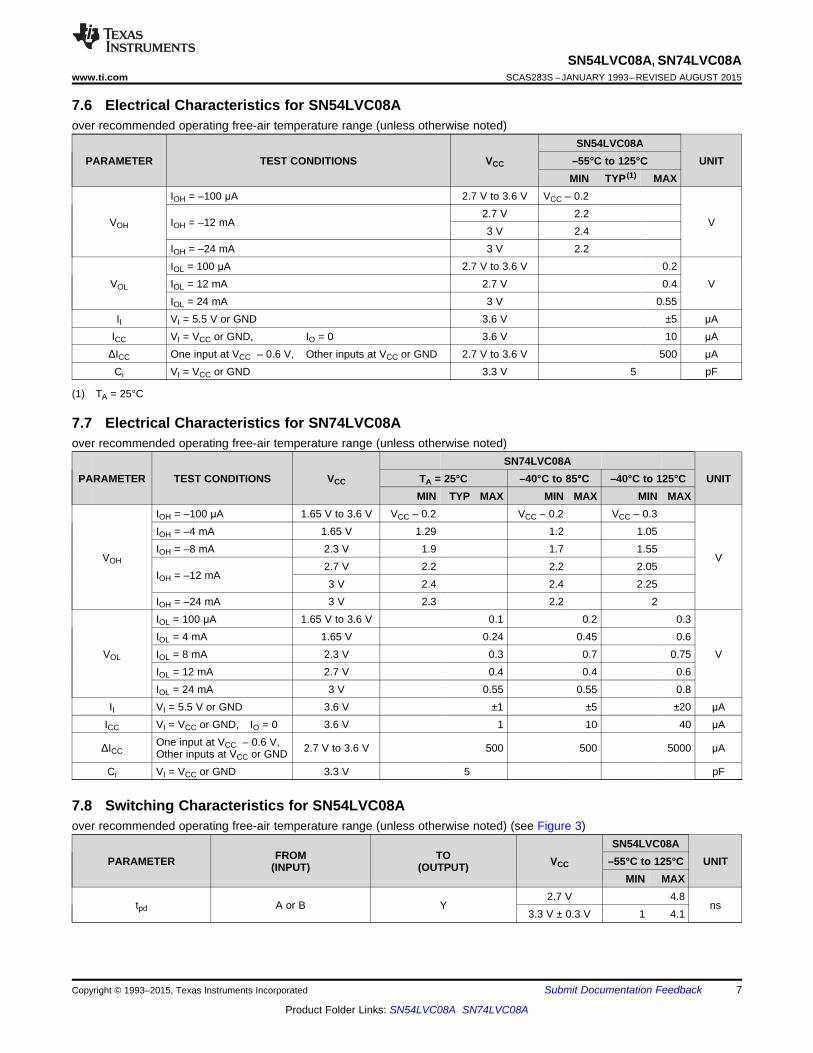
7.6 Electrical Characteristics for SN54LVC08Aover recommended operating free-air temperature range (unless otherwise noted)
SN54LVC08APARAMETER TEST CONDITIONS VCC –55°C to 125°C UNIT
MIN TYP (1) MAXIOH = –100 μA 2.7 V to 3.6 V VCC – 0.2
2.7 V 2.2VOH IOH = –12 mA V
3 V 2.4IOH = –24 mA 3 V 2.2IOL = 100 μA 2.7 V to 3.6 V 0.2
VOL IOL = 12 mA 2.7 V 0.4 VIOL = 24 mA 3 V 0.55
II VI = 5.5 V or GND 3.6 V ±5 μAICC VI = VCC or GND, IO = 0 3.6 V 10 μAΔICC One input at VCC – 0.6 V, Other inputs at VCC or GND 2.7 V to 3.6 V 500 μA
Ci VI = VCC or GND 3.3 V 5 pF
(1) TA = 25°C
7.7 Electrical Characteristics for SN74LVC08Aover recommended operating free-air temperature range (unless otherwise noted)
SN74LVC08APARAMETER TEST CONDITIONS VCC TA = 25°C –40°C to 85°C –40°C to 125°C UNIT
MIN TYP MAX MIN MAX MIN MAXIOH = –100 μA 1.65 V to 3.6 V VCC – 0.2 VCC – 0.2 VCC – 0.3IOH = –4 mA 1.65 V 1.29 1.2 1.05IOH = –8 mA 2.3 V 1.9 1.7 1.55
VOH V2.7 V 2.2 2.2 2.05
IOH = –12 mA3 V 2.4 2.4 2.25
IOH = –24 mA 3 V 2.3 2.2 2IOL = 100 μA 1.65 V to 3.6 V 0.1 0.2 0.3IOL = 4 mA 1.65 V 0.24 0.45 0.6
VOL IOL = 8 mA 2.3 V 0.3 0.7 0.75 VIOL = 12 mA 2.7 V 0.4 0.4 0.6IOL = 24 mA 3 V 0.55 0.55 0.8
II VI = 5.5 V or GND 3.6 V ±1 ±5 ±20 μAICC VI = VCC or GND, IO = 0 3.6 V 1 10 40 μA
One input at VCC – 0.6 V,ΔICC 2.7 V to 3.6 V 500 500 5000 μAOther inputs at VCC or GNDCi VI = VCC or GND 3.3 V 5 pF
7.8 Switching Characteristics for SN54LVC08Aover recommended operating free-air temperature range (unless otherwise noted) (see Figure 3)
SN54LVC08AFROM TOPARAMETER VCC –55°C to 125°C UNIT(INPUT) (OUTPUT)
MIN MAX2.7 V 4.8
tpd A or B Y ns3.3 V ± 0.3 V 1 4.1
Copyright © 1993–2015, Texas Instruments Incorporated Submit Documentation Feedback 7
Product Folder Links: SN54LVC08A SN74LVC08A

2
4
6
8
10
12
14
0 50 100 150 200 250 300
CL – Load Capacitance – pF
VCC = 3 V,
TA = 25°C
One Output Switching
Four Outputs Switching
Eight Outputs Switching
t–
Pro
pag
ati
on
Dela
yT
ime
–n
sp
d
2
4
6
8
10
0 50 100 150 200 250 300
CL – Load Capacitance – pF
t–
Pro
pa
ga
tio
nD
ela
yT
ime
–n
sp
d
VCC = 3 V,
TA = 25°C
One Output Switching
Four Outputs Switching
Eight Outputs Switching
SN54LVC08A, SN74LVC08ASCAS283S –JANUARY 1993–REVISED AUGUST 2015 www.ti.com
7.9 Switching Characteristics for SN74LVC08Aover recommended operating free-air temperature range (unless otherwise noted) (see Figure 3)
SN74LVC08AFROM TOPARAMETER VCC TA = 25°C –40°C to 85°C –40°C to 125°C UNIT(INPUT) (OUTPUT)
MIN TYP MAX MIN MAX MIN MAX1.8 V ± 0.15 V 1 5 9.3 1 9.8 1 11.32.5 V ± 0.2 V 1 2.9 6.4 1 6.9 1 9
tpd A or B Y ns2.7 V 1 3 4.6 1 4.8 1 6
3.3 V ± 0.3 V 1 2.6 3.9 1 4.1 1 5.5tsk(o) 3.3 V ± 0.3 V 1 1.5 ns
7.10 Operating CharacteristicsTA = 25°C
TESTPARAMETER VCC TYP UNITCONDITIONS1.8 V 7
Cpd Power dissipation capacitance per gate f = 10 MHz 2.5 V 9.8 pF3.3 V 10
7.11 Typical Characteristics
Figure 1. Propagation Delay (Low to High Transition) Figure 2. Propagation Delay (High to Low Transition)vs Load Capacitance vs Load Capacitance
8 Submit Documentation Feedback Copyright © 1993–2015, Texas Instruments Incorporated
Product Folder Links: SN54LVC08A SN74LVC08A

VM
thtsu
From Output
Under Test
CL
(see Note A)
LOAD CIRCUIT
S1
VLOAD
Open
GND
RL
RL
Data Input
Timing Input
VI
0 V
VI
0 V0 V
tw
Input
VOLTAGE WAVEFORMS
SETUP AND HOLD TIMES
VOLTAGE WAVEFORMS
PROPAGATION DELAY TIMES
INVERTING AND NONINVERTING OUTPUTS
VOLTAGE WAVEFORMS
PULSE DURATION
tPLH
tPHL
tPHL
tPLH
VOH
VOH
VOL
VOL
VI
0 VInput
Output
Waveform 1
S1 at VLOAD
(see Note B)
Output
Waveform 2
S1 at GND
(see Note B)
VOL
VOH
tPZL
tPZH
tPLZ
tPHZ
VLOAD/2
0 V
VOL + VD
VOH - VD
≈0 V
VI
VOLTAGE WAVEFORMS
ENABLE AND DISABLE TIMES
LOW- AND HIGH-LEVEL ENABLING
Output
Output
tPLH/tPHL
tPLZ/tPZL
tPHZ/tPZH
Open
VLOAD
GND
TEST S1
NOTES: A. CL includes probe and jig capacitance.
B. Waveform 1 is for an output with internal conditions such that the output is low, except when disabled by the output control.
Waveform 2 is for an output with internal conditions such that the output is high, except when disabled by the output control.
C. All input pulses are supplied by generators having the following characteristics: PRR≤ 10 MHz, ZO = 50 W.
D. The outputs are measured one at a time, with one transition per measurement.
E. tPLZ and tPHZ are the same as tdis.
F. tPZL and tPZH are the same as ten.
G. tPLH and tPHL are the same as tpd.
H. All parameters and waveforms are not applicable to all devices.
Output
Control
VM VM
VM VM
VM VM
VM
VM VM
VM
VM
VM
VI
VM
VM
1.8 V ± 0.15 V
2.5 V ± 0.2 V
2.7 V
3.3 V ± 0.3 V
1 kΩ
500 Ω
500 Ω
500 Ω
VCC RL
2 × VCC
2 × VCC
6 V
6 V
VLOAD CL
30 pF
30 pF
50 pF
50 pF
0.15 V
0.15 V
0.3 V
0.3 V
VD
VCC
VCC
2.7 V
2.7 V
VI
VCC/2
VCC/2
1.5 V
1.5 V
VMtr/tf
≤2 ns
≤2 ns
≤2.5 ns
≤2.5 ns
INPUTS
SN54LVC08A, SN74LVC08Awww.ti.com SCAS283S –JANUARY 1993–REVISED AUGUST 2015
8 Parameter Measurement Information
Figure 3. Load Circuit and Voltage Waveforms
Copyright © 1993–2015, Texas Instruments Incorporated Submit Documentation Feedback 9
Product Folder Links: SN54LVC08A SN74LVC08A

A
BY
SN54LVC08A, SN74LVC08ASCAS283S –JANUARY 1993–REVISED AUGUST 2015 www.ti.com
9 Detailed Description
9.1 OverviewThe SN74LVC08 device contains quadruple 2-input positive AND gate device and performs the Boolean functionY= A ·B. This device is useful when multiple AND function is used in the system.
9.2 Functional Block Diagram
Figure 4. Logic Diagram, Each Gate (Positive Logic)
9.3 Feature DescriptionThe device can operate from 1.65 V to 3.6 V, allowing to be used in low voltage systems.
The device can accept voltages to 5.5 V make this device flexible to connect and work seamlessly with widevoltage range systems.
The maximum tpd of 4.1 ns at 3.3 V is beneficial for use in high speed applications.
The device has a Ioff support live insertion, a partial-power-down mode, and a back-drive protection.
9.4 Device Functional ModesTable 1 lists the functional modes for the SN54LVC08A and SN74LVC08A devices.
Table 1. Truth TableINPUTS OUTPUT
A B YH H HL X LX L L
10 Submit Documentation Feedback Copyright © 1993–2015, Texas Instruments Incorporated
Product Folder Links: SN54LVC08A SN74LVC08A

A
B
Y
C
R
SN54LVC08A, SN74LVC08Awww.ti.com SCAS283S –JANUARY 1993–REVISED AUGUST 2015
10 Application and Implementation
NOTEInformation in the following applications sections is not part of the TI componentspecification, and TI does not warrant its accuracy or completeness. TI’s customers areresponsible for determining suitability of components for their purposes. Customers shouldvalidate and test their design implementation to confirm system functionality.
10.1 Application InformationThe SN74LVC08A is used to drive CMOS device and used for implementing AND logic. LVC famiy can supportcurrent drive of about 24 mA at 3-V VCC. The inputs for SN74LVC08 are 5.5-V tolerant allowing it to translatedown to VCC.
10.2 Typical Application
Figure 5. Three Input AND Gate Implementation and Driving LED
10.2.1 Design RequirementsThis device uses CMOS technology and has balanced output drive. Take care to avoid bus contention because itcan drive currents that would exceed maximum limits. The high drive will also create fast edges into light loadsso routing and load conditions should be considered to prevent ringing.
10.2.2 Detailed Design ProcedureSN74LVC08A contains four AND gates in one package which can be used for individual AND function or toimplement complex Bolean logic. Figure 5 shows an example of implementing 3input AND function. AB areinputs for AND gate which are connected to another AND gate. Z= A·B·C. SN74LVC08A support high drivecurrent of 24 mA which can be used to drive LED's of even Drive low current signal FETs, an example is shownin Figure 5 TI recommends to use a series resistance to limit the current. If VCC is 3 V, and LED current shouldbe 10 mA, and the forward-voltage of LED is 2.5 V, then R as shown in Figure 5 is calculated using Equation 1below:
R = (VCC – VLED) / I (1)R = (3 – 2.5) / 0.01 = 50 Ω
Copyright © 1993–2015, Texas Instruments Incorporated Submit Documentation Feedback 11
Product Folder Links: SN54LVC08A SN74LVC08A

VCC
Unused Input
Input
Output Output
Input
Unused Input
–100
–80
–60
–40
–20
0
20
40
60
–1 –0.5 0.0 0.5 1.0 1.5 2.0 2.5 3.0 3.5 4.0
TA = 25°C, VCC = 3 V,
VIH = 3 V, VIL = 0 V,
All Outputs Switching
VOH – VI O
H–
mA
VOL – V
–20
0
20
40
60
80
100
–0.2 0.0 0.2 0.4 0.6 0.8 1.0 1.2 1.4 1.6
TA = 25°C, VCC = 3 V,
VIH = 3 V, VIL = 0 V,
All Outputs Switching
I OL
–m
A
SN54LVC08A, SN74LVC08ASCAS283S –JANUARY 1993–REVISED AUGUST 2015 www.ti.com
Typical Application (continued)10.2.3 Application Curves
Figure 6. Output Drive Current (IOL) Figure 7. Output Drive Current (IOH)vs LOW-level Output Voltage (VOL) vs HIGH-level Output Voltage (VOH)
11 Power Supply RecommendationsThe power supply can be any voltage between the minimum and maximum supply voltage rating located inthe Recommended Operating Conditions table.Each VCC pin should have a good bypass capacitor to prevent power disturbance. For devices with a singlesupply, a 0.1-μF capacitor is recommended and if there are multiple VCC pins then 0.01-μF or 0.022-μFcapacitor is recommended for each power pin. It is ok to parallel multiple bypass capacitors to reject differentfrequencies of noise. 0.1-μF and 1-μF capacitors are commonly used in parallel. The bypass capacitorshould be installed as close to the power pin as possible for best results.
12 Layout
12.1 Layout GuidelinesWhen using multiple bit logic devices inputs should not ever float. In many cases, functions or parts offunctions of digital logic devices are unused; for example, when only two inputs of a triple-input AND gate areused or only 3 of the 4 buffer gates are used. Such input pins should not be left unconnected because theundefined voltages at the outside connections result in undefined operational states. Specified below are therules that must be observed under all circumstances. All unused inputs of digital logic devices must beconnected to a high or low bias to prevent them from floating. The logic level that should be applied to anyparticular unused input depends on the function of the device. Generally they will be tied to GND or VCCwhichever make more sense or is more convenient.
12.2 Layout Examples
Figure 8. Layout Examples
12 Submit Documentation Feedback Copyright © 1993–2015, Texas Instruments Incorporated
Product Folder Links: SN54LVC08A SN74LVC08A

SN54LVC08A, SN74LVC08Awww.ti.com SCAS283S –JANUARY 1993–REVISED AUGUST 2015
13 Device and Documentation Support
13.1 Related LinksThe table below lists quick access links. Categories include technical documents, support and communityresources, tools and software, and quick access to sample or buy.
Table 2. Related LinksTECHNICAL TOOLS & SUPPORT &PARTS PRODUCT FOLDER SAMPLE & BUY DOCUMENTS SOFTWARE COMMUNITY
SN54LVC08A Click here Click here Click here Click here Click hereSN74LVC08A Click here Click here Click here Click here Click here
13.2 Community ResourcesThe following links connect to TI community resources. Linked contents are provided "AS IS" by the respectivecontributors. They do not constitute TI specifications and do not necessarily reflect TI's views; see TI's Terms ofUse.
TI E2E™ Online Community TI's Engineer-to-Engineer (E2E) Community. Created to foster collaborationamong engineers. At e2e.ti.com, you can ask questions, share knowledge, explore ideas and helpsolve problems with fellow engineers.
Design Support TI's Design Support Quickly find helpful E2E forums along with design support tools andcontact information for technical support.
13.3 TrademarksE2E is a trademark of Texas Instruments.All other trademarks are the property of their respective owners.
13.4 Electrostatic Discharge CautionThese devices have limited built-in ESD protection. The leads should be shorted together or the device placed in conductive foamduring storage or handling to prevent electrostatic damage to the MOS gates.
13.5 GlossarySLYZ022 — TI Glossary.
This glossary lists and explains terms, acronyms, and definitions.
14 Mechanical, Packaging, and Orderable InformationThe following pages include mechanical packaging and orderable information. This information is the mostcurrent data available for the designated devices. This data is subject to change without notice and revision ofthis document. For browser based versions of this data sheet, refer to the left hand navigation.
Copyright © 1993–2015, Texas Instruments Incorporated Submit Documentation Feedback 13
Product Folder Links: SN54LVC08A SN74LVC08A

PACKAGE OPTION ADDENDUM
www.ti.com 15-Apr-2017
Addendum-Page 1
PACKAGING INFORMATION
Orderable Device Status(1)
Package Type PackageDrawing
Pins PackageQty
Eco Plan(2)
Lead/Ball Finish(6)
MSL Peak Temp(3)
Op Temp (°C) Device Marking(4/5)
Samples
5962-9753401Q2A ACTIVE LCCC FK 20 1 TBD POST-PLATE N / A for Pkg Type -55 to 125 5962-9753401Q2ASNJ54LVC08AFK
5962-9753401QCA ACTIVE CDIP J 14 1 TBD A42 N / A for Pkg Type -55 to 125 5962-9753401QCASNJ54LVC08AJ
5962-9753401QDA ACTIVE CFP W 14 1 TBD A42 N / A for Pkg Type -55 to 125 5962-9753401QDASNJ54LVC08AW
HVAL02231ARGYR ACTIVE VQFN RGY 14 3000 Green (RoHS& no Sb/Br)
CU NIPDAU Level-2-260C-1 YEAR -40 to 125 LC08A
SN74LVC08AD ACTIVE SOIC D 14 50 Green (RoHS& no Sb/Br)
CU NIPDAU Level-1-260C-UNLIM -40 to 125 LVC08A
SN74LVC08ADBR ACTIVE SSOP DB 14 2000 Green (RoHS& no Sb/Br)
CU NIPDAU Level-1-260C-UNLIM -40 to 125 LC08A
SN74LVC08ADBRE4 ACTIVE SSOP DB 14 2000 Green (RoHS& no Sb/Br)
CU NIPDAU Level-1-260C-UNLIM -40 to 125 LC08A
SN74LVC08ADBRG4 ACTIVE SSOP DB 14 2000 Green (RoHS& no Sb/Br)
CU NIPDAU Level-1-260C-UNLIM -40 to 125 LC08A
SN74LVC08ADE4 ACTIVE SOIC D 14 50 Green (RoHS& no Sb/Br)
CU NIPDAU Level-1-260C-UNLIM -40 to 125 LVC08A
SN74LVC08ADG4 ACTIVE SOIC D 14 50 Green (RoHS& no Sb/Br)
CU NIPDAU Level-1-260C-UNLIM -40 to 125 LVC08A
SN74LVC08ADR ACTIVE SOIC D 14 2500 Green (RoHS& no Sb/Br)
CU NIPDAU | CU SN Level-1-260C-UNLIM -40 to 125 LVC08A
SN74LVC08ADRE4 ACTIVE SOIC D 14 2500 Green (RoHS& no Sb/Br)
CU NIPDAU Level-1-260C-UNLIM -40 to 125 LVC08A
SN74LVC08ADRG3 ACTIVE SOIC D 14 2500 Green (RoHS& no Sb/Br)
CU SN Level-1-260C-UNLIM -40 to 125 LVC08A
SN74LVC08ADRG4 ACTIVE SOIC D 14 2500 Green (RoHS& no Sb/Br)
CU NIPDAU Level-1-260C-UNLIM -40 to 125 LVC08A
SN74LVC08ADT ACTIVE SOIC D 14 250 Green (RoHS& no Sb/Br)
CU NIPDAU Level-1-260C-UNLIM -40 to 125 LVC08A

PACKAGE OPTION ADDENDUM
www.ti.com 15-Apr-2017
Addendum-Page 2
Orderable Device Status(1)
Package Type PackageDrawing
Pins PackageQty
Eco Plan(2)
Lead/Ball Finish(6)
MSL Peak Temp(3)
Op Temp (°C) Device Marking(4/5)
Samples
SN74LVC08ANSR ACTIVE SO NS 14 2000 Green (RoHS& no Sb/Br)
CU NIPDAU Level-1-260C-UNLIM -40 to 125 LVC08A
SN74LVC08ANSRE4 ACTIVE SO NS 14 2000 Green (RoHS& no Sb/Br)
CU NIPDAU Level-1-260C-UNLIM -40 to 125 LVC08A
SN74LVC08APW ACTIVE TSSOP PW 14 90 Green (RoHS& no Sb/Br)
CU NIPDAU Level-1-260C-UNLIM -40 to 125 LC08A
SN74LVC08APWE4 ACTIVE TSSOP PW 14 90 Green (RoHS& no Sb/Br)
CU NIPDAU Level-1-260C-UNLIM -40 to 125 LC08A
SN74LVC08APWG4 ACTIVE TSSOP PW 14 90 Green (RoHS& no Sb/Br)
CU NIPDAU Level-1-260C-UNLIM -40 to 125 LC08A
SN74LVC08APWR ACTIVE TSSOP PW 14 2000 Green (RoHS& no Sb/Br)
CU NIPDAU | CU SN Level-1-260C-UNLIM -40 to 125 LC08A
SN74LVC08APWRE4 ACTIVE TSSOP PW 14 2000 Green (RoHS& no Sb/Br)
CU NIPDAU Level-1-260C-UNLIM -40 to 125 LC08A
SN74LVC08APWRG3 ACTIVE TSSOP PW 14 2000 Green (RoHS& no Sb/Br)
CU SN Level-1-260C-UNLIM -40 to 125 LC08A
SN74LVC08APWRG4 ACTIVE TSSOP PW 14 2000 Green (RoHS& no Sb/Br)
CU NIPDAU Level-1-260C-UNLIM -40 to 125 LC08A
SN74LVC08APWT ACTIVE TSSOP PW 14 250 Green (RoHS& no Sb/Br)
CU NIPDAU Level-1-260C-UNLIM -40 to 125 LC08A
SN74LVC08APWTG4 ACTIVE TSSOP PW 14 250 Green (RoHS& no Sb/Br)
CU NIPDAU Level-1-260C-UNLIM -40 to 125 LC08A
SN74LVC08ARGYR ACTIVE VQFN RGY 14 3000 Green (RoHS& no Sb/Br)
CU NIPDAU Level-2-260C-1 YEAR -40 to 125 LC08A
SN74LVC08ARGYRG4 ACTIVE VQFN RGY 14 3000 Green (RoHS& no Sb/Br)
CU NIPDAU Level-2-260C-1 YEAR -40 to 125 LC08A
SNJ54LVC08AFK ACTIVE LCCC FK 20 1 TBD POST-PLATE N / A for Pkg Type -55 to 125 5962-9753401Q2ASNJ54LVC08AFK
SNJ54LVC08AJ ACTIVE CDIP J 14 1 TBD A42 N / A for Pkg Type -55 to 125 5962-9753401QCASNJ54LVC08AJ
SNJ54LVC08AW ACTIVE CFP W 14 1 TBD A42 N / A for Pkg Type -55 to 125 5962-9753401QDASNJ54LVC08AW

PACKAGE OPTION ADDENDUM
www.ti.com 15-Apr-2017
Addendum-Page 3
(1) The marketing status values are defined as follows:ACTIVE: Product device recommended for new designs.LIFEBUY: TI has announced that the device will be discontinued, and a lifetime-buy period is in effect.NRND: Not recommended for new designs. Device is in production to support existing customers, but TI does not recommend using this part in a new design.PREVIEW: Device has been announced but is not in production. Samples may or may not be available.OBSOLETE: TI has discontinued the production of the device.
(2) Eco Plan - The planned eco-friendly classification: Pb-Free (RoHS), Pb-Free (RoHS Exempt), or Green (RoHS & no Sb/Br) - please check http://www.ti.com/productcontent for the latest availabilityinformation and additional product content details.TBD: The Pb-Free/Green conversion plan has not been defined.Pb-Free (RoHS): TI's terms "Lead-Free" or "Pb-Free" mean semiconductor products that are compatible with the current RoHS requirements for all 6 substances, including the requirement thatlead not exceed 0.1% by weight in homogeneous materials. Where designed to be soldered at high temperatures, TI Pb-Free products are suitable for use in specified lead-free processes.Pb-Free (RoHS Exempt): This component has a RoHS exemption for either 1) lead-based flip-chip solder bumps used between the die and package, or 2) lead-based die adhesive used betweenthe die and leadframe. The component is otherwise considered Pb-Free (RoHS compatible) as defined above.Green (RoHS & no Sb/Br): TI defines "Green" to mean Pb-Free (RoHS compatible), and free of Bromine (Br) and Antimony (Sb) based flame retardants (Br or Sb do not exceed 0.1% by weightin homogeneous material)
(3) MSL, Peak Temp. - The Moisture Sensitivity Level rating according to the JEDEC industry standard classifications, and peak solder temperature.
(4) There may be additional marking, which relates to the logo, the lot trace code information, or the environmental category on the device.
(5) Multiple Device Markings will be inside parentheses. Only one Device Marking contained in parentheses and separated by a "~" will appear on a device. If a line is indented then it is a continuationof the previous line and the two combined represent the entire Device Marking for that device.
(6) Lead/Ball Finish - Orderable Devices may have multiple material finish options. Finish options are separated by a vertical ruled line. Lead/Ball Finish values may wrap to two lines if the finishvalue exceeds the maximum column width.
Important Information and Disclaimer:The information provided on this page represents TI's knowledge and belief as of the date that it is provided. TI bases its knowledge and belief on informationprovided by third parties, and makes no representation or warranty as to the accuracy of such information. Efforts are underway to better integrate information from third parties. TI has taken andcontinues to take reasonable steps to provide representative and accurate information but may not have conducted destructive testing or chemical analysis on incoming materials and chemicals.TI and TI suppliers consider certain information to be proprietary, and thus CAS numbers and other limited information may not be available for release.
In no event shall TI's liability arising out of such information exceed the total purchase price of the TI part(s) at issue in this document sold by TI to Customer on an annual basis.
OTHER QUALIFIED VERSIONS OF SN54LVC08A, SN74LVC08A :
• Catalog: SN74LVC08A
• Automotive: SN74LVC08A-Q1, SN74LVC08A-Q1

PACKAGE OPTION ADDENDUM
www.ti.com 15-Apr-2017
Addendum-Page 4
• Enhanced Product: SN74LVC08A-EP, SN74LVC08A-EP
• Military: SN54LVC08A
NOTE: Qualified Version Definitions:
• Catalog - TI's standard catalog product
• Automotive - Q100 devices qualified for high-reliability automotive applications targeting zero defects
• Enhanced Product - Supports Defense, Aerospace and Medical Applications
• Military - QML certified for Military and Defense Applications
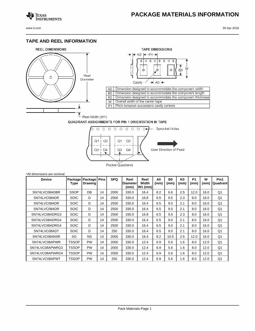
TAPE AND REEL INFORMATION
*All dimensions are nominal
Device PackageType
PackageDrawing
Pins SPQ ReelDiameter
(mm)
ReelWidth
W1 (mm)
A0(mm)
B0(mm)
K0(mm)
P1(mm)
W(mm)
Pin1Quadrant
SN74LVC08ADBR SSOP DB 14 2000 330.0 16.4 8.2 6.6 2.5 12.0 16.0 Q1
SN74LVC08ADR SOIC D 14 2500 330.0 16.8 6.5 9.5 2.3 8.0 16.0 Q1
SN74LVC08ADR SOIC D 14 2500 330.0 16.4 6.5 9.0 2.1 8.0 16.0 Q1
SN74LVC08ADR SOIC D 14 2500 330.0 16.4 6.5 9.0 2.1 8.0 16.0 Q1
SN74LVC08ADRG3 SOIC D 14 2500 330.0 16.8 6.5 9.5 2.3 8.0 16.0 Q1
SN74LVC08ADRG4 SOIC D 14 2500 330.0 16.4 6.5 9.0 2.1 8.0 16.0 Q1
SN74LVC08ADRG4 SOIC D 14 2500 330.0 16.4 6.5 9.0 2.1 8.0 16.0 Q1
SN74LVC08ADT SOIC D 14 250 330.0 16.4 6.5 9.0 2.1 8.0 16.0 Q1
SN74LVC08ANSR SO NS 14 2000 330.0 16.4 8.2 10.5 2.5 12.0 16.0 Q1
SN74LVC08APWR TSSOP PW 14 2000 330.0 12.4 6.9 5.6 1.6 8.0 12.0 Q1
SN74LVC08APWRG3 TSSOP PW 14 2000 330.0 12.4 6.9 5.6 1.6 8.0 12.0 Q1
SN74LVC08APWRG4 TSSOP PW 14 2000 330.0 12.4 6.9 5.6 1.6 8.0 12.0 Q1
SN74LVC08APWT TSSOP PW 14 250 330.0 12.4 6.9 5.6 1.6 8.0 12.0 Q1
PACKAGE MATERIALS INFORMATION
www.ti.com 30-Apr-2018
Pack Materials-Page 1

*All dimensions are nominal
Device Package Type Package Drawing Pins SPQ Length (mm) Width (mm) Height (mm)
SN74LVC08ADBR SSOP DB 14 2000 367.0 367.0 38.0
SN74LVC08ADR SOIC D 14 2500 364.0 364.0 27.0
SN74LVC08ADR SOIC D 14 2500 367.0 367.0 38.0
SN74LVC08ADR SOIC D 14 2500 333.2 345.9 28.6
SN74LVC08ADRG3 SOIC D 14 2500 364.0 364.0 27.0
SN74LVC08ADRG4 SOIC D 14 2500 333.2 345.9 28.6
SN74LVC08ADRG4 SOIC D 14 2500 367.0 367.0 38.0
SN74LVC08ADT SOIC D 14 250 367.0 367.0 38.0
SN74LVC08ANSR SO NS 14 2000 367.0 367.0 38.0
SN74LVC08APWR TSSOP PW 14 2000 367.0 367.0 35.0
SN74LVC08APWRG3 TSSOP PW 14 2000 364.0 364.0 27.0
SN74LVC08APWRG4 TSSOP PW 14 2000 367.0 367.0 35.0
SN74LVC08APWT TSSOP PW 14 250 367.0 367.0 35.0
PACKAGE MATERIALS INFORMATION
www.ti.com 30-Apr-2018
Pack Materials-Page 2


www.ti.com
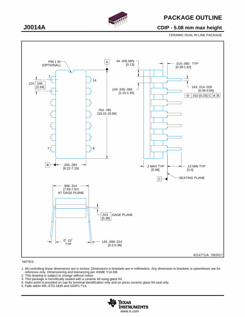
PACKAGE OUTLINE
C
14X .008-.014 [0.2-0.36]TYP
-150
AT GAGE PLANE
-.314.308-7.977.83[ ]
14X -.026.014-0.660.36[ ]14X -.065.045
-1.651.15[ ]
.2 MAX TYP[5.08]
.13 MIN TYP[3.3]
TYP-.060.015-1.520.38[ ]
4X .005 MIN[0.13]
12X .100[2.54]
.015 GAGE PLANE[0.38]
A
-.785.754-19.9419.15[ ]
B -.283.245-7.196.22[ ]
CDIP - 5.08 mm max heightJ0014ACERAMIC DUAL IN LINE PACKAGE
4214771/A 05/2017
NOTES: 1. All controlling linear dimensions are in inches. Dimensions in brackets are in millimeters. Any dimension in brackets or parenthesis are for reference only. Dimensioning and tolerancing per ASME Y14.5M.2. This drawing is subject to change without notice. 3. This package is hermitically sealed with a ceramic lid using glass frit.4. Index point is provided on cap for terminal identification only and on press ceramic glass frit seal only.5. Falls within MIL-STD-1835 and GDIP1-T14.
7 8
141
PIN 1 ID(OPTIONAL)
SCALE 0.900
SEATING PLANE
.010 [0.25] C A B

www.ti.com
EXAMPLE BOARD LAYOUT
ALL AROUND[0.05]
MAX.002
.002 MAX[0.05]ALL AROUND
SOLDER MASKOPENING
METAL
(.063)[1.6]
(R.002 ) TYP[0.05]
14X ( .039)[1]
( .063)[1.6]
12X (.100 )[2.54]
(.300 ) TYP[7.62]
CDIP - 5.08 mm max heightJ0014ACERAMIC DUAL IN LINE PACKAGE
4214771/A 05/2017
LAND PATTERN EXAMPLENON-SOLDER MASK DEFINED
SCALE: 5X
SEE DETAIL A SEE DETAIL B
SYMM
SYMM
1
7 8
14
DETAIL ASCALE: 15X
SOLDER MASKOPENING
METAL
DETAIL B13X, SCALE: 15X


MECHANICAL DATA
MSSO002E – JANUARY 1995 – REVISED DECEMBER 2001
POST OFFICE BOX 655303 • DALLAS, TEXAS 75265
DB (R-PDSO-G**) PLASTIC SMALL-OUTLINE
4040065 /E 12/01
28 PINS SHOWN
Gage Plane
8,207,40
0,550,95
0,25
38
12,90
12,30
28
10,50
24
8,50
Seating Plane
9,907,90
30
10,50
9,90
0,38
5,605,00
15
0,22
14
A
28
1
2016
6,506,50
14
0,05 MIN
5,905,90
DIM
A MAX
A MIN
PINS **
2,00 MAX
6,90
7,50
0,65 M0,15
0°–�8°
0,10
0,090,25
NOTES: A. All linear dimensions are in millimeters.B. This drawing is subject to change without notice.C. Body dimensions do not include mold flash or protrusion not to exceed 0,15.D. Falls within JEDEC MO-150

IMPORTANT NOTICE
Texas Instruments Incorporated (TI) reserves the right to make corrections, enhancements, improvements and other changes to itssemiconductor products and services per JESD46, latest issue, and to discontinue any product or service per JESD48, latest issue. Buyersshould obtain the latest relevant information before placing orders and should verify that such information is current and complete.TI’s published terms of sale for semiconductor products (http://www.ti.com/sc/docs/stdterms.htm) apply to the sale of packaged integratedcircuit products that TI has qualified and released to market. Additional terms may apply to the use or sale of other types of TI products andservices.Reproduction of significant portions of TI information in TI data sheets is permissible only if reproduction is without alteration and isaccompanied by all associated warranties, conditions, limitations, and notices. TI is not responsible or liable for such reproduceddocumentation. Information of third parties may be subject to additional restrictions. Resale of TI products or services with statementsdifferent from or beyond the parameters stated by TI for that product or service voids all express and any implied warranties for theassociated TI product or service and is an unfair and deceptive business practice. TI is not responsible or liable for any such statements.Buyers and others who are developing systems that incorporate TI products (collectively, “Designers”) understand and agree that Designersremain responsible for using their independent analysis, evaluation and judgment in designing their applications and that Designers havefull and exclusive responsibility to assure the safety of Designers' applications and compliance of their applications (and of all TI productsused in or for Designers’ applications) with all applicable regulations, laws and other applicable requirements. Designer represents that, withrespect to their applications, Designer has all the necessary expertise to create and implement safeguards that (1) anticipate dangerousconsequences of failures, (2) monitor failures and their consequences, and (3) lessen the likelihood of failures that might cause harm andtake appropriate actions. Designer agrees that prior to using or distributing any applications that include TI products, Designer willthoroughly test such applications and the functionality of such TI products as used in such applications.TI’s provision of technical, application or other design advice, quality characterization, reliability data or other services or information,including, but not limited to, reference designs and materials relating to evaluation modules, (collectively, “TI Resources”) are intended toassist designers who are developing applications that incorporate TI products; by downloading, accessing or using TI Resources in anyway, Designer (individually or, if Designer is acting on behalf of a company, Designer’s company) agrees to use any particular TI Resourcesolely for this purpose and subject to the terms of this Notice.TI’s provision of TI Resources does not expand or otherwise alter TI’s applicable published warranties or warranty disclaimers for TIproducts, and no additional obligations or liabilities arise from TI providing such TI Resources. TI reserves the right to make corrections,enhancements, improvements and other changes to its TI Resources. TI has not conducted any testing other than that specificallydescribed in the published documentation for a particular TI Resource.Designer is authorized to use, copy and modify any individual TI Resource only in connection with the development of applications thatinclude the TI product(s) identified in such TI Resource. NO OTHER LICENSE, EXPRESS OR IMPLIED, BY ESTOPPEL OR OTHERWISETO ANY OTHER TI INTELLECTUAL PROPERTY RIGHT, AND NO LICENSE TO ANY TECHNOLOGY OR INTELLECTUAL PROPERTYRIGHT OF TI OR ANY THIRD PARTY IS GRANTED HEREIN, including but not limited to any patent right, copyright, mask work right, orother intellectual property right relating to any combination, machine, or process in which TI products or services are used. Informationregarding or referencing third-party products or services does not constitute a license to use such products or services, or a warranty orendorsement thereof. Use of TI Resources may require a license from a third party under the patents or other intellectual property of thethird party, or a license from TI under the patents or other intellectual property of TI.TI RESOURCES ARE PROVIDED “AS IS” AND WITH ALL FAULTS. TI DISCLAIMS ALL OTHER WARRANTIES ORREPRESENTATIONS, EXPRESS OR IMPLIED, REGARDING RESOURCES OR USE THEREOF, INCLUDING BUT NOT LIMITED TOACCURACY OR COMPLETENESS, TITLE, ANY EPIDEMIC FAILURE WARRANTY AND ANY IMPLIED WARRANTIES OFMERCHANTABILITY, FITNESS FOR A PARTICULAR PURPOSE, AND NON-INFRINGEMENT OF ANY THIRD PARTY INTELLECTUALPROPERTY RIGHTS. TI SHALL NOT BE LIABLE FOR AND SHALL NOT DEFEND OR INDEMNIFY DESIGNER AGAINST ANY CLAIM,INCLUDING BUT NOT LIMITED TO ANY INFRINGEMENT CLAIM THAT RELATES TO OR IS BASED ON ANY COMBINATION OFPRODUCTS EVEN IF DESCRIBED IN TI RESOURCES OR OTHERWISE. IN NO EVENT SHALL TI BE LIABLE FOR ANY ACTUAL,DIRECT, SPECIAL, COLLATERAL, INDIRECT, PUNITIVE, INCIDENTAL, CONSEQUENTIAL OR EXEMPLARY DAMAGES INCONNECTION WITH OR ARISING OUT OF TI RESOURCES OR USE THEREOF, AND REGARDLESS OF WHETHER TI HAS BEENADVISED OF THE POSSIBILITY OF SUCH DAMAGES.Unless TI has explicitly designated an individual product as meeting the requirements of a particular industry standard (e.g., ISO/TS 16949and ISO 26262), TI is not responsible for any failure to meet such industry standard requirements.Where TI specifically promotes products as facilitating functional safety or as compliant with industry functional safety standards, suchproducts are intended to help enable customers to design and create their own applications that meet applicable functional safety standardsand requirements. Using products in an application does not by itself establish any safety features in the application. Designers mustensure compliance with safety-related requirements and standards applicable to their applications. Designer may not use any TI products inlife-critical medical equipment unless authorized officers of the parties have executed a special contract specifically governing such use.Life-critical medical equipment is medical equipment where failure of such equipment would cause serious bodily injury or death (e.g., lifesupport, pacemakers, defibrillators, heart pumps, neurostimulators, and implantables). Such equipment includes, without limitation, allmedical devices identified by the U.S. Food and Drug Administration as Class III devices and equivalent classifications outside the U.S.TI may expressly designate certain products as completing a particular qualification (e.g., Q100, Military Grade, or Enhanced Product).Designers agree that it has the necessary expertise to select the product with the appropriate qualification designation for their applicationsand that proper product selection is at Designers’ own risk. Designers are solely responsible for compliance with all legal and regulatoryrequirements in connection with such selection.Designer will fully indemnify TI and its representatives against any damages, costs, losses, and/or liabilities arising out of Designer’s non-compliance with the terms and provisions of this Notice.
Mailing Address: Texas Instruments, Post Office Box 655303, Dallas, Texas 75265Copyright © 2018, Texas Instruments Incorporated