Scanning tunnelling microscopy and electronic structure Avdelningen för synkrotronljusfysik,...
15
Scanning tunnelling microscopy and electronic structure Avdelningen för synkrotronljusfysik, Fysiska institutionen, Lunds universitet Spektroskopi och materiens kvantmekaniska beskrivning FYS T20, VT 2008
-
Upload
clarissa-conley -
Category
Documents
-
view
226 -
download
6
Transcript of Scanning tunnelling microscopy and electronic structure Avdelningen för synkrotronljusfysik,...
Scanning tunnelling microscopyand
electronic structure
Avdelningen för synkrotronljusfysik, Fysiska institutionen, Lunds universitetSpektroskopi och materiens kvantmekaniska beskrivning FYS T20, VT 2008
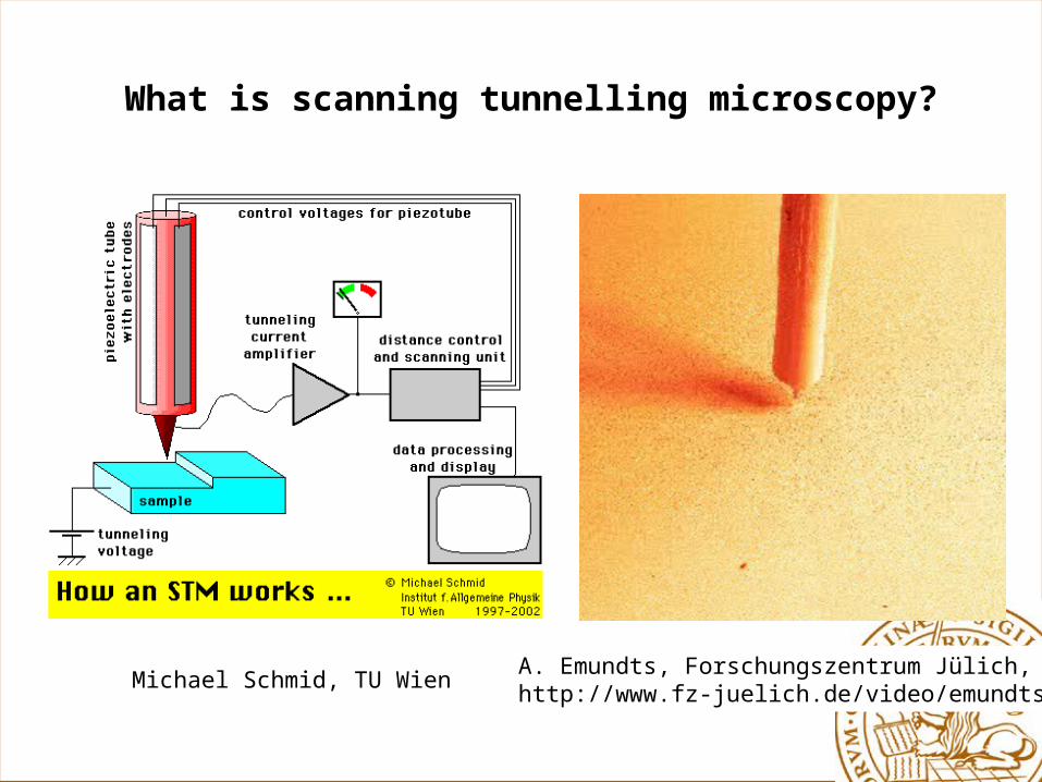
What is scanning tunnelling microscopy?
Michael Schmid, TU Wien A. Emundts, Forschungszentrum Jülich,http://www.fz-juelich.de/video/emundts/
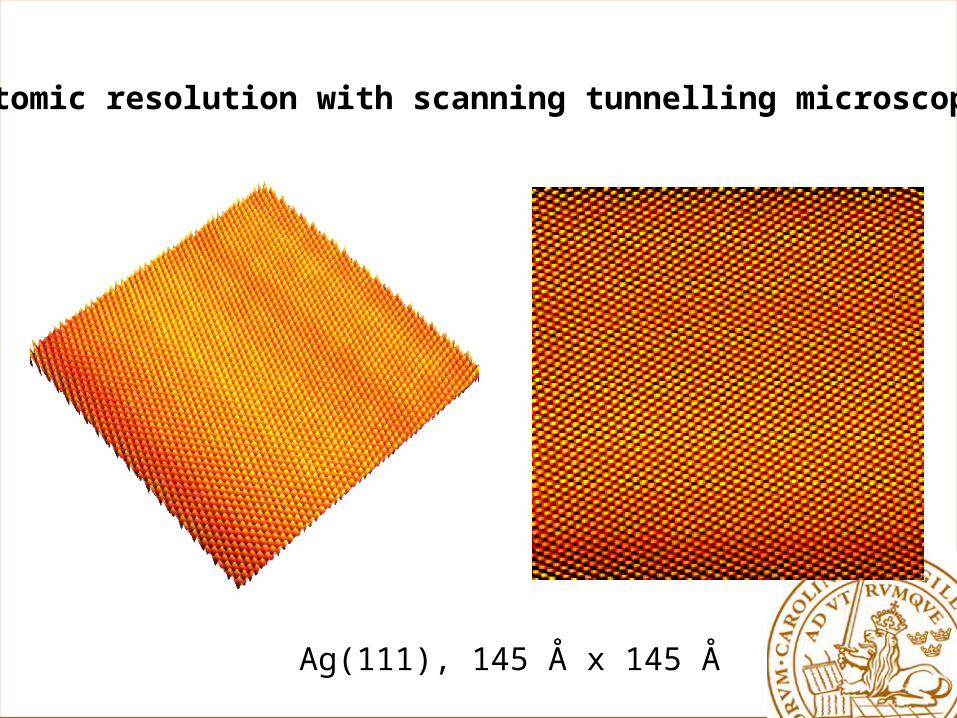
Ag(111), 145 Å x 145 Å
Atomic resolution with scanning tunnelling microscopy
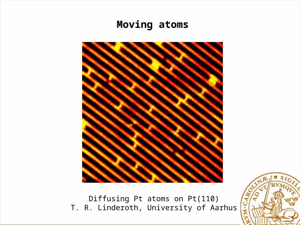
Moving atoms
Diffusing Pt atoms on Pt(110)T. R. Linderoth, University of Aarhus

The experimental geometry
V- +
Image from: Blanco et al., Prof. Surf. Sci. 81 (2006) 403
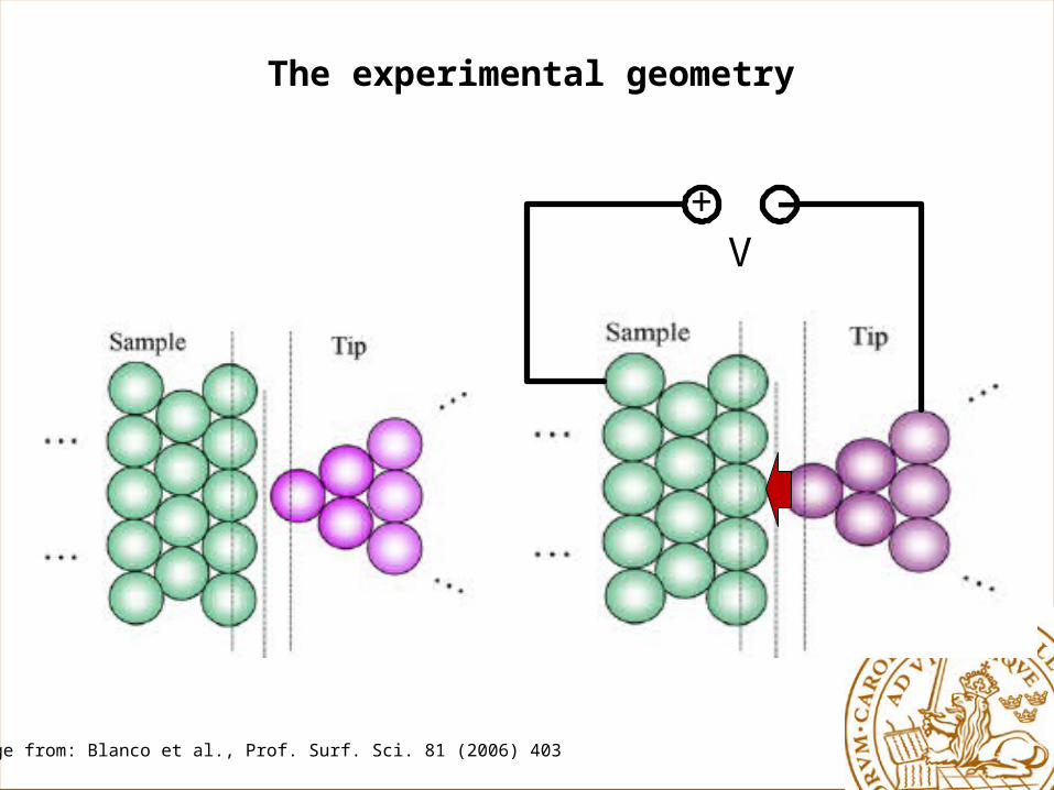
V-+
The experimental geometry
Image from: Blanco et al., Prof. Surf. Sci. 81 (2006) 403
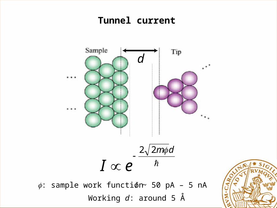
d
dm
eI22
Tunnel current
: sample work function I ~ 50 pA – 5 nA
Working d: around 5 Å
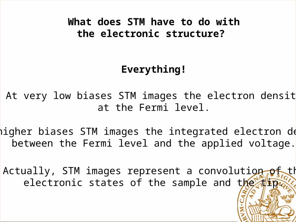
What does STM have to do withthe electronic structure?
Everything!
At very low biases STM images the electron densityat the Fermi level.
At higher biases STM images the integrated electron densitybetween the Fermi level and the applied voltage.
Actually, STM images represent a convolution of theelectronic states of the sample and the tip.
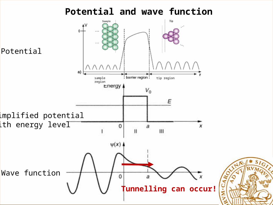
Potential
Simplified potentialwith energy level
Wave function
Potential and wave function
sample region
tip region
Tunnelling can occur!

EFermi EFermi
Energy
xSample Tip
EFermi
EFermi
Energy
xSample Tip
-eV
-eV
EFermi
EFermi
Energy
xSample Tip
No bias
Negative bias
Positive bias
Tunnel currents for homogeneous density of states
No net current
Positive net current
Negative net current
Conventions:- bias applied to sample- current measured on tip
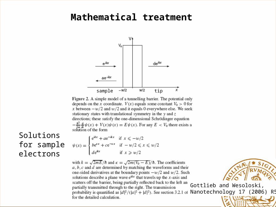
Mathematical treatment
Solutionsfor sampleelectrons
sample tip
Gottlieb and Wesoloski,Nanotechnology 17 (2006) R57
Pk
3x10⁻³
210-1-2-3E
k - (eV)
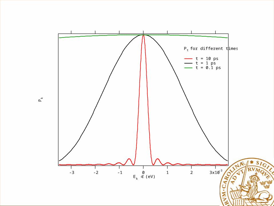
Pt for different times t
t = 10 ps t = 1 ps t = 0.1 ps
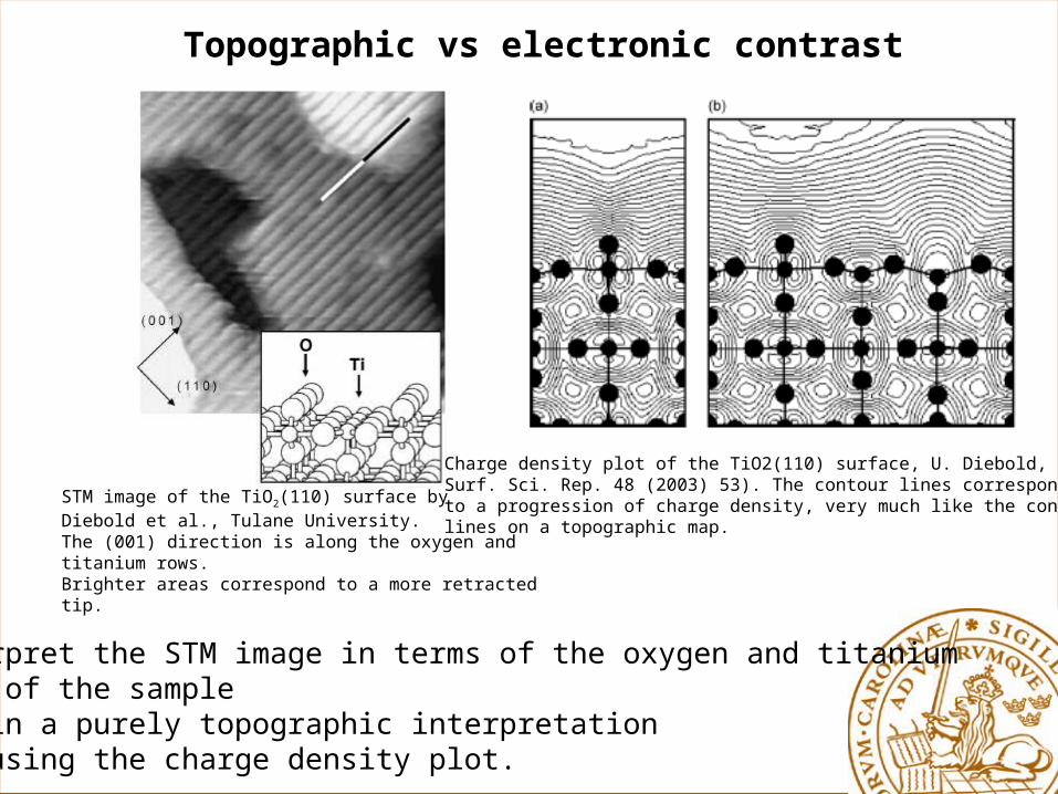
Topographic vs electronic contrast
STM image of the TiO2(110) surface byDiebold et al., Tulane University.The (001) direction is along the oxygen andtitanium rows.Brighter areas correspond to a more retractedtip.
Charge density plot of the TiO2(110) surface, U. Diebold,Surf. Sci. Rep. 48 (2003) 53). The contour lines correspondto a progression of charge density, very much like the contourlines on a topographic map.
Interpret the STM image in terms of the oxygen and titaniumrows of the sample(a) in a purely topographic interpretation(b) using the charge density plot.
EFermiEFermi
Energy
xSample Tip
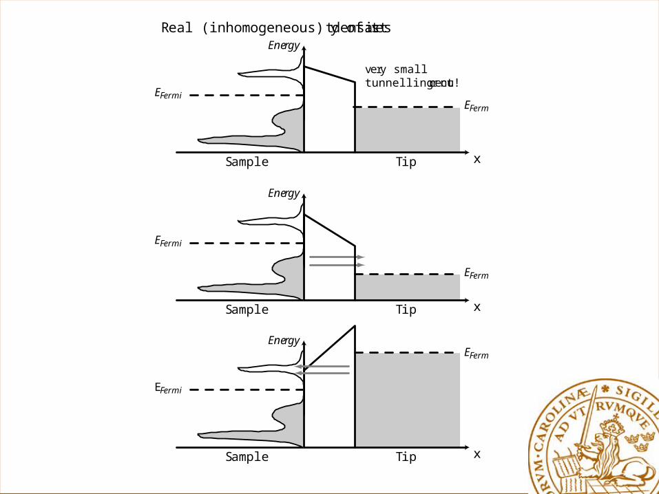
Real (inhomogeneous) density of states
EFermi
EFermi
Energy
xSample Tip
very smalltunnelling current!
EFermi
EFermi
Energy
xSample Tip
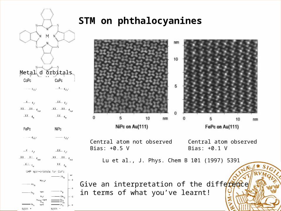
STM on phthalocyanines
Central atom not observedBias: +0.5 V
Central atom observedBias: +0.1 V
Lu et al., J. Phys. Chem B 101 (1997) 5391
Metal d orbitals
Give an interpretation of the differencein terms of what you’ve learnt!