Scanning transmission I. Mu¨llerova´ low-energy electron ... transmiss… · Scanning...
6
Scanning transmission low-energy electron microscopy I. Mu ¨ llerova ´ M. Hovorka I. Konvalina M. Unc ˇ ovsky ´ L. Frank We discuss an extension to the transmission mode of the cathode-lens-equipped scanning electron microscope, enabling operation down to the lowest energies of electrons. Penetration of electrons through free-standing ultrathin films is examined along the full energy scale, and the contribution of the secondary electrons (SEs), released near the bottom surface of the sample, is shown, enhancing the apparent transmissivity of the sample to more than 100%. Provisional filtering off of the SEs, providing the dark-field signal of forward-scattered electrons, was made using an annular 3-D adjustable detector inserted below the sample. Demonstration experiments were performed on the graphene flakes and on a 3-nm-thick carbon film. Electron penetrability at the lowest energies was measured on the graphene sample. Introduction The transmission electron microscope (TEM) is capable of imaging individual atomic columns and, at certain conditions, even single atoms in free-standing thin foils using electrons in the energy range of hundreds of kiloelectronvolts. The scanning TEM (STEM) mode is also operated in the same energy range, mostly in the form of an attachment to a TEM device. Significant effort has been invested in achieving high resolution, even at lower energies, where we obtain lesser radiation damage and higher contrast [1]. Even sub-Ångstro ¨m resolution was presented at 20 keV in an aberration-corrected TEM [2]. Recently, even low atomic number materials, such as carbon structures and biological samples or polymers, can be imaged with high contrast and lateral resolution [3–5]. Since about two decades ago, STEM attachments to the scanning electron microscopes (SEMs), which are normally used for imaging of bulk samples, started appearing more broadly [6, 7]. These are operated at energies that are usually available in the SEM, i.e., up to approximately 30 keV. Adequately thinner samples of 100 or 200 nm in thickness must be used in this case. However, the inelastic mean-free path, which is primarily responsible for the electron penetration, starts steeply growing again below approximately 50 eV (see, e.g., [8]). This establishes an approach to operating the STEM at tens or units of electronvolts on samples of thicknesses around or below 10 nm. More than 40 years ago, Kanter published a possibility of transmission of 1.1-eV electrons through a self-supported gold film with a thickness of 20 or 5 nm [9]. One of the first experimental setups for the measurement of transmissivity through self-supported thin films was designed by Smith and Wells [10]. In order to avoid aberrations of lenses for the long wavelength of electrons at very low energies, they used a Blensless[ system in which the source of electrons (at units of electronvolts) was placed just 1 nm above the specimen and mechanically scanned across the surface while the transmitted signal was detected. Regrettably, no results obtained with this setup have been published. Thin films condensed on a metal substrate were examined using irradiation by a monoenergetic electron beam at energies below 30 eV via the signal transmitted through the surface layer into the underlying specimen and measured as the so-called absorbed current (see the overview of Sanche [11]). We made use of the advantages of the cathode lens (CL) principle [12] to obtain high lateral resolution in the SEM down to very low energies [16]. The microscope was equipped with the detector of not only reflected electrons but also transmitted electrons (TEs). Initial results have shown the method to be a powerful tool for the examination of ultrathin films [13–15]. This paper describes imaging of 3-nm carbon foils in the reflected and transmitted mode at ÓCopyright 2011 by International Business Machines Corporation. Copying in printed form for private use is permitted without payment of royalty provided that (1) each reproduction is done without alteration and (2) the Journal reference and IBM copyright notice are included on the first page. The title and abstract, but no other portions, of this paper may be copied by any means or distributed royalty free without further permission by computer-based and other information-service systems. Permission to republish any other portion of this paper must be obtained from the Editor. I. MU ¨ LLEROVA ´ ET AL. 2:1 IBM J. RES. & DEV. VOL. 55 NO. 4 PAPER 2 JULY/AUGUST 2011 0018-8646/11/$5.00 B 2011 IBM Digital Object Identifier: 10.1147/JRD.2011.2156190
Transcript of Scanning transmission I. Mu¨llerova´ low-energy electron ... transmiss… · Scanning...

Scanning transmissionlow-energy electronmicroscopy
I. MullerovaM. HovorkaI. Konvalina
M. UncovskyL. Frank
We discuss an extension to the transmission mode of thecathode-lens-equipped scanning electron microscope, enablingoperation down to the lowest energies of electrons. Penetration ofelectrons through free-standing ultrathin films is examined along thefull energy scale, and the contribution of the secondary electrons(SEs), released near the bottom surface of the sample, is shown,enhancing the apparent transmissivity of the sample to morethan 100%. Provisional filtering off of the SEs, providing thedark-field signal of forward-scattered electrons, was made usingan annular 3-D adjustable detector inserted below the sample.Demonstration experiments were performed on the graphene flakesand on a 3-nm-thick carbon film. Electron penetrability at thelowest energies was measured on the graphene sample.
IntroductionThe transmission electron microscope (TEM) is capableof imaging individual atomic columns and, at certainconditions, even single atoms in free-standing thin foilsusing electrons in the energy range of hundreds ofkiloelectronvolts. The scanning TEM (STEM) mode is alsooperated in the same energy range, mostly in the form of anattachment to a TEM device. Significant effort has beeninvested in achieving high resolution, even at lower energies,where we obtain lesser radiation damage and highercontrast [1]. Even sub-Ångstrom resolution was presentedat 20 keV in an aberration-corrected TEM [2]. Recently,even low atomic number materials, such as carbon structuresand biological samples or polymers, can be imaged withhigh contrast and lateral resolution [3–5].Since about two decades ago, STEM attachments to the
scanning electron microscopes (SEMs), which are normallyused for imaging of bulk samples, started appearing morebroadly [6, 7]. These are operated at energies that are usuallyavailable in the SEM, i.e., up to approximately 30 keV.Adequately thinner samples of 100 or 200 nm in thicknessmust be used in this case.However, the inelastic mean-free path, which is primarily
responsible for the electron penetration, starts steeplygrowing again below approximately 50 eV (see, e.g., [8]).
This establishes an approach to operating the STEM attens or units of electronvolts on samples of thicknessesaround or below 10 nm. More than 40 years ago, Kanterpublished a possibility of transmission of 1.1-eV electronsthrough a self-supported gold film with a thickness of 20or 5 nm [9]. One of the first experimental setups for themeasurement of transmissivity through self-supported thinfilms was designed by Smith and Wells [10]. In order toavoid aberrations of lenses for the long wavelength ofelectrons at very low energies, they used a Blensless[ systemin which the source of electrons (at units of electronvolts)was placed just 1 nm above the specimen and mechanicallyscanned across the surface while the transmitted signalwas detected. Regrettably, no results obtained with thissetup have been published. Thin films condensed on ametal substrate were examined using irradiation by amonoenergetic electron beam at energies below 30 eV viathe signal transmitted through the surface layer into theunderlying specimen and measured as the so-called absorbedcurrent (see the overview of Sanche [11]).We made use of the advantages of the cathode lens (CL)
principle [12] to obtain high lateral resolution in the SEMdown to very low energies [16]. The microscope wasequipped with the detector of not only reflected electrons butalso transmitted electrons (TEs). Initial results have shownthe method to be a powerful tool for the examination ofultrathin films [13–15]. This paper describes imaging of3-nm carbon foils in the reflected and transmitted mode at
�Copyright 2011 by International Business Machines Corporation. Copying in printed form for private use is permitted without payment of royalty provided that (1) each reproduction is done withoutalteration and (2) the Journal reference and IBM copyright notice are included on the first page. The title and abstract, but no other portions, of this paper may be copied by any means or distributed
royalty free without further permission by computer-based and other information-service systems. Permission to republish any other portion of this paper must be obtained from the Editor.
I. MULLEROVA ET AL. 2 : 1IBM J. RES. & DEV. VOL. 55 NO. 4 PAPER 2 JULY/AUGUST 2011
0018-8646/11/$5.00 B 2011 IBM
Digital Object Identifier: 10.1147/JRD.2011.2156190
low energies and with high-resolution imaging of thegraphene [16] in both signals at very low energies.
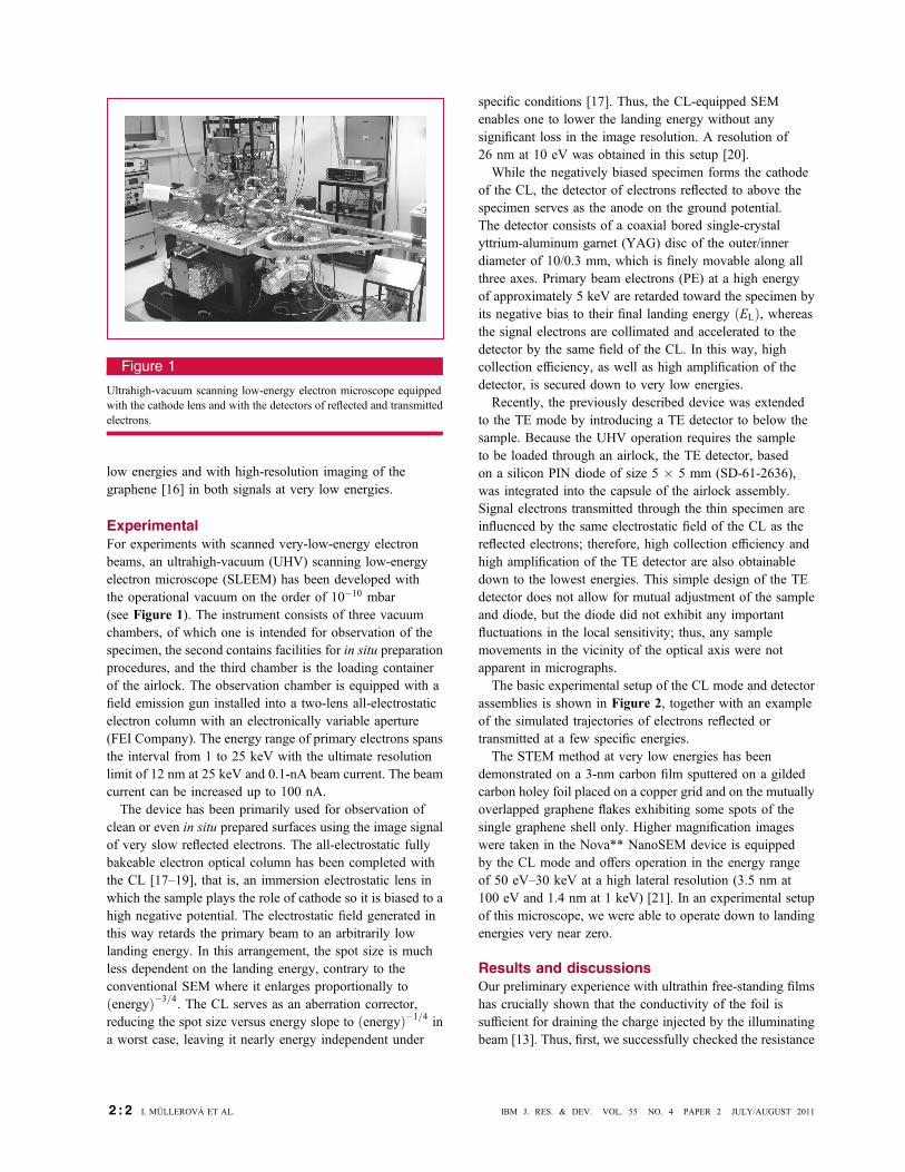
ExperimentalFor experiments with scanned very-low-energy electronbeams, an ultrahigh-vacuum (UHV) scanning low-energyelectron microscope (SLEEM) has been developed withthe operational vacuum on the order of 10�10 mbar(see Figure 1). The instrument consists of three vacuumchambers, of which one is intended for observation of thespecimen, the second contains facilities for in situ preparationprocedures, and the third chamber is the loading containerof the airlock. The observation chamber is equipped with afield emission gun installed into a two-lens all-electrostaticelectron column with an electronically variable aperture(FEI Company). The energy range of primary electrons spansthe interval from 1 to 25 keV with the ultimate resolutionlimit of 12 nm at 25 keV and 0.1-nA beam current. The beamcurrent can be increased up to 100 nA.The device has been primarily used for observation of
clean or even in situ prepared surfaces using the image signalof very slow reflected electrons. The all-electrostatic fullybakeable electron optical column has been completed withthe CL [17–19], that is, an immersion electrostatic lens inwhich the sample plays the role of cathode so it is biased to ahigh negative potential. The electrostatic field generated inthis way retards the primary beam to an arbitrarily lowlanding energy. In this arrangement, the spot size is muchless dependent on the landing energy, contrary to theconventional SEM where it enlarges proportionally toðenergyÞ�3=4. The CL serves as an aberration corrector,reducing the spot size versus energy slope to ðenergyÞ�1=4 ina worst case, leaving it nearly energy independent under
specific conditions [17]. Thus, the CL-equipped SEMenables one to lower the landing energy without anysignificant loss in the image resolution. A resolution of26 nm at 10 eV was obtained in this setup [20].While the negatively biased specimen forms the cathode
of the CL, the detector of electrons reflected to above thespecimen serves as the anode on the ground potential.The detector consists of a coaxial bored single-crystalyttrium-aluminum garnet (YAG) disc of the outer/innerdiameter of 10/0.3 mm, which is finely movable along allthree axes. Primary beam electrons (PE) at a high energyof approximately 5 keV are retarded toward the specimen byits negative bias to their final landing energy ðELÞ, whereasthe signal electrons are collimated and accelerated to thedetector by the same field of the CL. In this way, highcollection efficiency, as well as high amplification of thedetector, is secured down to very low energies.Recently, the previously described device was extended
to the TE mode by introducing a TE detector to below thesample. Because the UHV operation requires the sampleto be loaded through an airlock, the TE detector, basedon a silicon PIN diode of size 5 � 5 mm (SD-61-2636),was integrated into the capsule of the airlock assembly.Signal electrons transmitted through the thin specimen areinfluenced by the same electrostatic field of the CL as thereflected electrons; therefore, high collection efficiency andhigh amplification of the TE detector are also obtainabledown to the lowest energies. This simple design of the TEdetector does not allow for mutual adjustment of the sampleand diode, but the diode did not exhibit any importantfluctuations in the local sensitivity; thus, any samplemovements in the vicinity of the optical axis were notapparent in micrographs.The basic experimental setup of the CL mode and detector
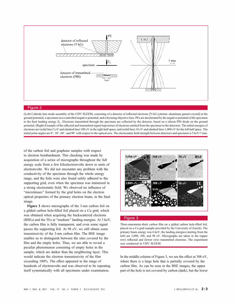
assemblies is shown in Figure 2, together with an exampleof the simulated trajectories of electrons reflected ortransmitted at a few specific energies.The STEM method at very low energies has been
demonstrated on a 3-nm carbon film sputtered on a gildedcarbon holey foil placed on a copper grid and on the mutuallyoverlapped graphene flakes exhibiting some spots of thesingle graphene shell only. Higher magnification imageswere taken in the Nova** NanoSEM device is equippedby the CL mode and offers operation in the energy rangeof 50 eV–30 keV at a high lateral resolution (3.5 nm at100 eV and 1.4 nm at 1 keV) [21]. In an experimental setupof this microscope, we were able to operate down to landingenergies very near zero.
Results and discussionsOur preliminary experience with ultrathin free-standing filmshas crucially shown that the conductivity of the foil issufficient for draining the charge injected by the illuminatingbeam [13]. Thus, first, we successfully checked the resistance
Figure 1
Ultrahigh-vacuum scanning low-energy electron microscope equippedwith the cathode lens and with the detectors of reflected and transmittedelectrons.
2 : 2 I. MULLEROVA ET AL. IBM J. RES. & DEV. VOL. 55 NO. 4 PAPER 2 JULY/AUGUST 2011
of the carbon foil and graphene samples with respectto electron bombardment. This checking was made byacquisition of a series of micrographs throughout the fullenergy scale from a few kiloelectronvolts down to units ofelectronvolts. We did not encounter any problem with theconductivity of the specimen through the whole energyrange, and the foils were also found safely adhered to thesupporting grid, even when the specimen was immersed ina strong electrostatic field. We observed no influence ofBmicrolenses[ formed by the grid holes on the electronoptical properties of the primary electron beam, in the finalimage.Figure 3 shows micrographs of the 3-nm carbon foil on
a gilded carbon hole-filled foil placed on a Cu grid, whichwas obtained when acquiring the backscattered electrons(BSEs) and the TEs at Bmedium[ landing energies. At 3 keV,the carbon film is fully transparent, and even some signalpasses the supporting foil. At 98 eV, we still obtain sometransmissivity of the 3-nm carbon film. The BSE imageenables us to distinguish between the sites covered by thefilm and the empty holes. Thus, we are able to reveal apeculiar phenomenon consisting of empty holes in thesample, which are darker than the neighboring layer. Thiswould indicate the electron transmissivity of the filmexceeding 100%. The effect appeared in the range ofhundreds of electronvolts and was observed to be repeatingitself systematically with all specimens under examination.
In the middle column of Figure 3, we see the effect at 308 eV,where there is a large hole that is partially covered by thecarbon film. As can be seen in the BSE images, the upperpart of the hole is not covered by carbon (dark), but the lower
Figure 3
Three-nanometer-thick carbon film on a gilded carbon hole-filled foil,placed on a Cu grid (sample provided by the University of Zurich). Theprimary beam energy was 6 keV; the landing energies (starting from theleft) are 3,000, 308, and 98 eV. Micrographs are taken in the (upperrow) reflected and (lower row) transmitted electrons. The experimentwas conducted in UHV SLEEM.
Figure 2
(Left) Cathode lens mode assembly of the UHV SLEEM, consisting of a detector of reflected electrons [YAG (yttrium–aluminum garnet) crystal] at theground potential, a specimen on a controlled negative potential, and a focusing objective lens. PEs are decelerated by the negative potential of the specimento the final landing energy EL. Electrons transmitted through the specimen are collected by the detector, based on a silicon PIN diode on the groundpotential. (Right) Example of the reflected and transmitted signal trajectories of electrons emitted from the specimen to the detectors. The initial energies ofelectrons are (solid line) 5 eV and (dashed line) 300 eV in the right half space, and (solid line) 10 eV and (dashed line) 1,000 eV for the left half space. Theinitial polar angles are 0�, 30�, 60�, and 90� with respect to the optical axis. The electrostatic field strength between detectors and specimen is 5 keV/7 mm.
I. MULLEROVA ET AL. 2 : 3IBM J. RES. & DEV. VOL. 55 NO. 4 PAPER 2 JULY/AUGUST 2011

part is (bright). However, in the TE image (308 eV), theholes appear darker than the carbon-covered regions.An explanation involves the unscattered and
forward-scattered electron signal, that is, the signal of theTEs from the illumination beam, which is significantlycontributed by Bincoherent[ secondary electrons (SEs)released near the bottom surface of the sample. The detectedyield of SE increases at low energies and exhibits itsmaximum just in the range of hundreds of electronvolts,similarly as it does with the SEs emitted to above theupper surface of a bulk specimen. The SE emitted from thebottom surface is released by both primary and scatteredelectrons penetrating to the near-surface layer through therest of the specimen. These exciting species must have muchbroader energy and angular distributions than the primaryelectrons alone, which bombard the SE emitting layer nearthe upper surface. However, the SE emitted in the reflectionmode from bulk specimens also contains SEII released byBSE upon their return toward the surface. When the energyof electrons decreases, one would expect in the emissionfrom the bottom surface a higher proportion of SEII, which isreleased with primary electrons that had survived somescattering events. This is due to the progressively shorteningmean-free path and the increasing rate of the elastic scatteringthat broadens the bundle of electrons penetrating the layer.Consequently, the signal from the bottom surface can beexpected to be less defined and hence less capable of bearingany useful information, except a possible thickness contrast.This is why we call this signal contribution Bincoherent[and consider it undesirable. Obviously, one has to be verycareful with interpretation of the TE flux measured behindthin samples at medium and low energies.Let us note that, although SEs are similarly generated in
any STEM device, in the absence of a field between thesample and the detector, they are too slow to be detected.In our case, SEs are accelerated toward the TE detector toenergy sufficient for the generation of the signal. However,at landing energies in and above the range of tens ofelectronvolts, the SEs are collimated near the optical axis,leaving the elastically scattered electrons concentrated in abroader bundle. This difference in trajectories, playing therole of energy dispersion, suggests that energy filtering toremove the SE signal is possible.In order to suppress the SE contribution to the signal,
an upgraded version of the TE detector was introduced.The TE detector was split into two concentric channels,similar to the way the bright-field and dark-field channels arearranged in a conventional STEM. This design enabled usto direct SE completely to the central channel (naturallytogether with a part of unscattered electrons of thebright-field signal), whereas the annular channel acquiresthe forward scattered electrons as the dark-field signal(see the simulated electron trajectories in Figure 2). Theupgraded version of the TE detector with the PIN diode,
which is already fully adjustable in all three directions, isinserted inside the sample capsule through a side opening.The proper diode has its central circular part of 1 mm indiameter etched off; thus, it is made Bblind,[ leavingundamaged correct functioning around the spot. Thus, weobtain functionless the central Bbright-field channel,[ butthe retractable mechanism enables one to center the diodeto the optical axis and to detect the sole dark-field signalfree of SEs or to shift it off the axis and collect thecomplete transmitted signal, at least at tens and units ofelectronvolts [22].Figure 4 shows a series of micrographs of the mutually
overlapped graphene flakes, which were taken at very lowenergies. The reflected signal images serve to identifyholes in the graphene.An interesting property of a filmlike graphene is its
transmissivity for electrons at various energies. These datamay be important in applications utilizing the film as asupport, e.g., for the point-projection electron microscopy atlow energies [23, 24]. The transmissivity was measuredbelow 30 eV in the total transmitted flux mode in severalspots on the sample where only a single graphene shellcould be expected. We found a transmissivity minimum at10 eV and maximum at 5 eV, and then, the transmittedflux decreases toward 1 eV. Obviously, electron energyclose to 5 eV (see Figure 4) is optimal when using thegraphene as a transparent support for any electronmicroscopic or spectroscopic mode. However, anisotropyof slow-electron passage through graphene [25] has to betaken into account.
Figure 4
Graphene deposited on a supporting grid, shown in the reflected mode(BSE, upper row) and in the transmitted signal (TE, lower row). Theprimary beam energy was 6 keV; the landing energies (starting from theleft) are 11, 5, and 3 eV. The specimen was provided by Geim fromthe University of Manchester as part of the EU STREP Project 028326.The experiment was conducted in the UHV SLEEM.
2 : 4 I. MULLEROVA ET AL. IBM J. RES. & DEV. VOL. 55 NO. 4 PAPER 2 JULY/AUGUST 2011
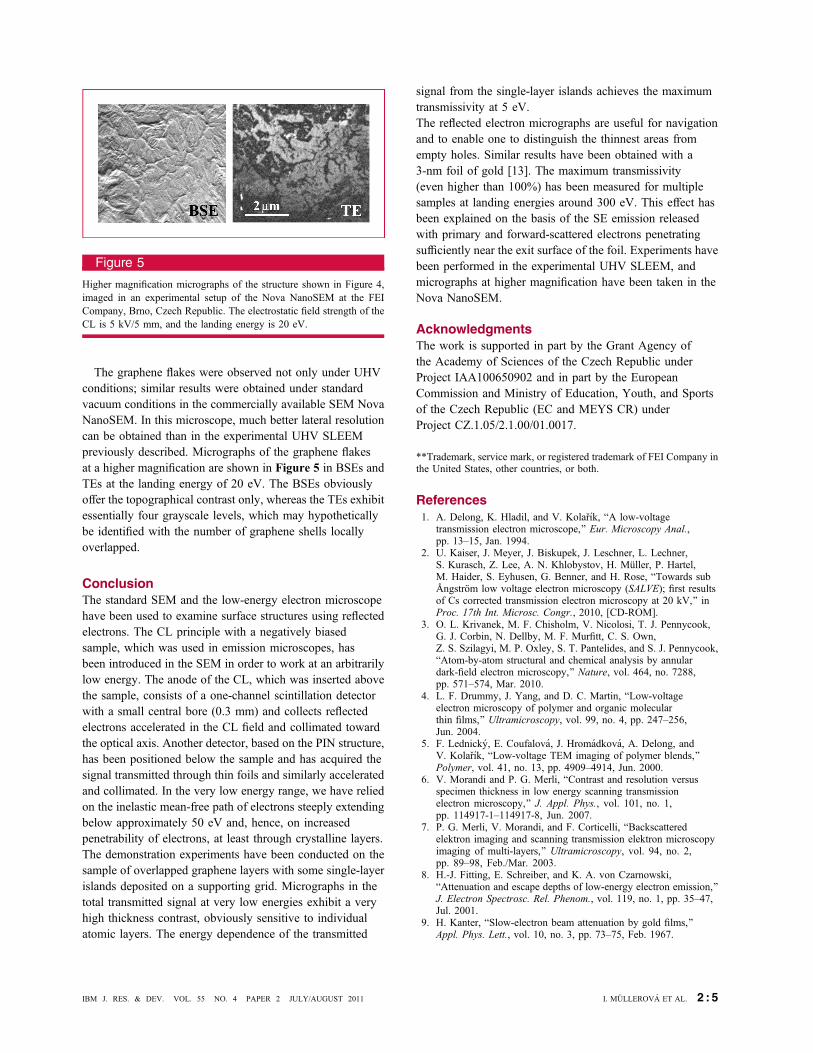
The graphene flakes were observed not only under UHVconditions; similar results were obtained under standardvacuum conditions in the commercially available SEM NovaNanoSEM. In this microscope, much better lateral resolutioncan be obtained than in the experimental UHV SLEEMpreviously described. Micrographs of the graphene flakesat a higher magnification are shown in Figure 5 in BSEs andTEs at the landing energy of 20 eV. The BSEs obviouslyoffer the topographical contrast only, whereas the TEs exhibitessentially four grayscale levels, which may hypotheticallybe identified with the number of graphene shells locallyoverlapped.
ConclusionThe standard SEM and the low-energy electron microscopehave been used to examine surface structures using reflectedelectrons. The CL principle with a negatively biasedsample, which was used in emission microscopes, hasbeen introduced in the SEM in order to work at an arbitrarilylow energy. The anode of the CL, which was inserted abovethe sample, consists of a one-channel scintillation detectorwith a small central bore (0.3 mm) and collects reflectedelectrons accelerated in the CL field and collimated towardthe optical axis. Another detector, based on the PIN structure,has been positioned below the sample and has acquired thesignal transmitted through thin foils and similarly acceleratedand collimated. In the very low energy range, we have reliedon the inelastic mean-free path of electrons steeply extendingbelow approximately 50 eV and, hence, on increasedpenetrability of electrons, at least through crystalline layers.The demonstration experiments have been conducted on thesample of overlapped graphene layers with some single-layerislands deposited on a supporting grid. Micrographs in thetotal transmitted signal at very low energies exhibit a veryhigh thickness contrast, obviously sensitive to individualatomic layers. The energy dependence of the transmitted
signal from the single-layer islands achieves the maximumtransmissivity at 5 eV.The reflected electron micrographs are useful for navigationand to enable one to distinguish the thinnest areas fromempty holes. Similar results have been obtained with a3-nm foil of gold [13]. The maximum transmissivity(even higher than 100%) has been measured for multiplesamples at landing energies around 300 eV. This effect hasbeen explained on the basis of the SE emission releasedwith primary and forward-scattered electrons penetratingsufficiently near the exit surface of the foil. Experiments havebeen performed in the experimental UHV SLEEM, andmicrographs at higher magnification have been taken in theNova NanoSEM.
AcknowledgmentsThe work is supported in part by the Grant Agency ofthe Academy of Sciences of the Czech Republic underProject IAA100650902 and in part by the EuropeanCommission and Ministry of Education, Youth, and Sportsof the Czech Republic (EC and MEYS CR) underProject CZ.1.05/2.1.00/01.0017.
**Trademark, service mark, or registered trademark of FEI Company inthe United States, other countries, or both.
References1. A. Delong, K. Hladil, and V. Kolarık, BA low-voltage
transmission electron microscope,[ Eur. Microscopy Anal.,pp. 13–15, Jan. 1994.
2. U. Kaiser, J. Meyer, J. Biskupek, J. Leschner, L. Lechner,S. Kurasch, Z. Lee, A. N. Khlobystov, H. Muller, P. Hartel,M. Haider, S. Eyhusen, G. Benner, and H. Rose, BTowards subÅngstrom low voltage electron microscopy (SALVE); first resultsof Cs corrected transmission electron microscopy at 20 kV,[ inProc. 17th Int. Microsc. Congr., 2010, [CD-ROM].
3. O. L. Krivanek, M. F. Chisholm, V. Nicolosi, T. J. Pennycook,G. J. Corbin, N. Dellby, M. F. Murfitt, C. S. Own,Z. S. Szilagyi, M. P. Oxley, S. T. Pantelides, and S. J. Pennycook,BAtom-by-atom structural and chemical analysis by annulardark-field electron microscopy,[ Nature, vol. 464, no. 7288,pp. 571–574, Mar. 2010.
4. L. F. Drummy, J. Yang, and D. C. Martin, BLow-voltageelectron microscopy of polymer and organic molecularthin films,[ Ultramicroscopy, vol. 99, no. 4, pp. 247–256,Jun. 2004.
5. F. Lednicky, E. Coufalova, J. Hromadkova, A. Delong, andV. Kolarık, BLow-voltage TEM imaging of polymer blends,[Polymer, vol. 41, no. 13, pp. 4909–4914, Jun. 2000.
6. V. Morandi and P. G. Merli, BContrast and resolution versusspecimen thickness in low energy scanning transmissionelectron microscopy,[ J. Appl. Phys., vol. 101, no. 1,pp. 114917-1–114917-8, Jun. 2007.
7. P. G. Merli, V. Morandi, and F. Corticelli, BBackscatteredelektron imaging and scanning transmission elektron microscopyimaging of multi-layers,[ Ultramicroscopy, vol. 94, no. 2,pp. 89–98, Feb./Mar. 2003.
8. H.-J. Fitting, E. Schreiber, and K. A. von Czarnowski,BAttenuation and escape depths of low-energy electron emission,[J. Electron Spectrosc. Rel. Phenom., vol. 119, no. 1, pp. 35–47,Jul. 2001.
9. H. Kanter, BSlow-electron beam attenuation by gold films,[Appl. Phys. Lett., vol. 10, no. 3, pp. 73–75, Feb. 1967.
Figure 5
Higher magnification micrographs of the structure shown in Figure 4,imaged in an experimental setup of the Nova NanoSEM at the FEICompany, Brno, Czech Republic. The electrostatic field strength of theCL is 5 kV/5 mm, and the landing energy is 20 eV.
I. MULLEROVA ET AL. 2 : 5IBM J. RES. & DEV. VOL. 55 NO. 4 PAPER 2 JULY/AUGUST 2011

10. D. A. Smith and O. C. Wells, BLow-energy scanning transmissionelectron microscope,[ U.S. Patent 4 618 767, 1986.
11. L. Sanche, BInteractions of low-energy electrons with atomicand molecular solids,[ Scanning Microsc., vol. 9, no. 3,pp. 619–656, 1995.
12. A. Recknagel, BTheorie des elektrischen Elektronenmikroskopsfur Selbststrahler,[ Z. Phys., vol. 117, no. 11/12, pp. 689–708,Aug. 1941.
13. I. Mullerova, M. Hovorka, J. Sobota, R. Hanzlıkova,T. Fort, and L. Frank, BTransmission through thin films by lowenergy scanning electron microscopy,[ in Proc. MC, vol. 1,G. Kothleitner and M. Leisch, Eds., Graz, Austria, 2009, vol. 1,pp. 163–164.
14. I. Mullerova, M. Hovorka, and L. Frank, BAdvances in lowenergy scanning electron microscopy,[ in Proc. 17th Int. Microsc.Conf., Rio de Janeiro, Brazil, 2010, pp. 256–257.
15. I. Mullerova, M. Hovorka, R. Hanzlıkova, and L. Frank,BVery low energy scanning microscopy of free-standingultrathin films,[ Mater. Trans., vol. 51, no. 2, pp. 265–270,2010.
16. P. Blake, E. W. Hill, A. H. Castro Neto, K. S. Novoselov, D. Jiang,R. Yang, T. J. Booth, and A. K. Geim, BMaking graphene visible,[Appl. Phys. Lett., vol. 91, no. 6, pp. 063124-1–063124-3,Aug. 2007.
17. I. Mullerova and L. Frank, BScanning low-energy electronmicroscopy,[ Adv. Imag. Electron Phys., vol. 128, pp. 309–443,2003.
18. I. Mullerova and L. Frank, BVery low energy microscopy incommercial SEMs,[ Scanning, vol. 15, no. 4, pp. 193–201,1993.
19. L. Frank and I. Mullerova, BStrategies for low- andvery-low-energy SEM,[ J. Electron Microsc., vol. 48, no. 3,pp. 205–219, 1999.
20. I. Mullerova and L. Frank, BUltrahigh vacuum scanninglow energy electron microscope (UHV SLEEM) for surfacestudies,[ in Proc. 2nd Annu. Meeting Czechoslovak Microsc. Soc.,L. Frank, Ed., 2002, pp. 79–82.
21. FEI Company, Nova NanoSEM Scanning ElectronMicroscope. [Online]. Available: http://www.fei.com/products/scanning-electron-microscopes/nova.aspx
22. I. Mullerova, M. Hovorka, and L. Frank, BExamination of verythin free-standing films with slow electrons,[ in Proc. JCNCS,Toyama, Japan, 2010, pp. 1–4.
23. H.-W. Fink and H. Schmid, BAtomic resolution in lenslesslow-energy electron holography,[ Phys. Rev. Lett., vol. 67, no. 12,pp. 1543–1546, Sep. 1991.
24. H.-W. Fink, H. Schmid, E. Ermantraut, and T. Schulz,BElectron holography of individual DNA molecules,[ J. Opt.Soc. Amer. A, Opt. Image Sci. Vis., vol. 14, no. 9, pp. 2168–2172,Sep. 1997.
25. R. M. Tromp, BLow energy electron microscopy: A 10 yearoutlook,[ in Proc. 14th Eur. Microsc. Congr., vol. 1, M. Luysberg,K. Tillmann, and T. Weirich, Eds., Aachen, Germany, 2008, vol. 1,pp. 735–736.
Received October 11, 2010; accepted for publicationFebruary 14, 2011
Ilona Mullerova Institute of Scientific Instruments ASCR,v.v.i., Kralovopolska 147, 612 64 Brno, Czech Republic([email protected]).
Milos Hovorka Institute of Scientific Instruments ASCR,v.v.i., Kralovopolska 147, 612 64 Brno, Czech Republic([email protected]).
Ivo Konvalina Institute of Scientific Instruments ASCR, v.v.i.,Kralovopolska 147, 612 64 Brno, Czech Republic ([email protected]).
Marek Uncovsky FEI Czech Republic s.r.o., Podnikatelska 6,61200 Brno, Czech Republic, ([email protected]).
Ludek Frank Institute of Scientific Instruments ASCR,v.v.i., Kralovopolska 147, 612 64 Brno, Czech Republic([email protected]).
2 : 6 I. MULLEROVA ET AL. IBM J. RES. & DEV. VOL. 55 NO. 4 PAPER 2 JULY/AUGUST 2011