SCANNING PROBE MICROSCOPY STUDIES OF … · SCANNING PROBE MICROSCOPY STUDIES ... Department of...
20
SCANNING PROBE MICROSCOPY STUDIES OF COPPER ELECTRODEPOSITION Richard J. Nichols, Department of Chemistry, The University of Liverpool, POBox 147, Liverpool, UK L69 3BX. ABSTRACT. The electrodeposition of bulk copper onto gold has proven to be a valuable model system for studying fine details of metal deposition processes with in-situ scanning probe microscopy (SPM). This chapter reviews the major in-situ SPM studies of bulk copper deposition and highlights the valuable sub- microscopic information which can be obtained with these techniques. Particular emphasis is placed on describing the growth morphology of the deposit and the effect of organic additives and the substrate surface. Finally, copper deposition on conductive polypyrrole is presented. 1.0. Introduction The electrodeposition of metals involves a sequence of rather distinct steps. The metal ions in solution diffuse to the electrode surface where they are discharged to form ad-atoms following partial or complete loss of their solvation sheath. The ad-atoms then cluster to form nuclei. These nuclei grow to form a deposit, whose morphological and crystallographic characteristics are typically very dependent on the precise deposition conditions. The nucleation and initial growth of the electrodeposit involves highly localised phenomena occurring on the substrate surface. Clearly, our understanding can be further enhanced by methods which enable us to examine the details of such processes at the sub-microscopic level. In-situ scanning probe microscopies (SPM) are able to provide a highly localised view of the electrode surface and deposit with an unprecedented resolution and have been successful in offering new insights into metal deposition processes. This chapter is concerned with the initial stages of bulk copper electrodeposition on gold and polypyrrole substrates, as directly observed using in-situ STM and AFM. Work previously covered in several individual articles is reviewed in this chapter, with an emphasis being placed here on tying together various aspects of the copper electrodeposition [1-6]. The initial formation of copper clusters on the metal surface and the subsequent growth of these centres is presented. The influence of organic additives on the growth of the copper deposit is also presented. Growth modes for the copper deposit are characterised and discussed for copper and polypyrrole substrates, with and without electrolyte additives. 2.0. Experimental Aspects The methodology and experimental procedure of in-situ STM have been discussed elsewhere [4,7-10]. Generally two methods have been used to examine bulk metal electrodeposits by in- situ STM. One method involves first retracting the tip from the surface and then depositing the metal [11-14]. The tip is then re-engaged in tunnelling mode and the deposit imaged. The other method entails continuous scanning ofthe surface, even during electrodeposition [1-6, 15-19]. 163 A. A. Gewirth and H. Siegenthaler (eds.). Nanoscale Probes of the Solid/Liquid Interface. 163-182. © 1995 Kluwer Academic Publishers.
Transcript of SCANNING PROBE MICROSCOPY STUDIES OF … · SCANNING PROBE MICROSCOPY STUDIES ... Department of...
SCANNING PROBE MICROSCOPY STUDIES OF COPPER ELECTRODEPOSITION
Richard J. Nichols, Department of Chemistry, The University of Liverpool, POBox 147, Liverpool, UK L69 3BX.
ABSTRACT. The electrodeposition of bulk copper onto gold has proven to be a valuable model system for studying fine details of metal deposition processes with in-situ scanning probe microscopy (SPM). This chapter reviews the major in-situ SPM studies of bulk copper deposition and highlights the valuable submicroscopic information which can be obtained with these techniques. Particular emphasis is placed on describing the growth morphology of the deposit and the effect of organic additives and the substrate surface. Finally, copper deposition on conductive polypyrrole is presented.
1.0. Introduction
The electrodeposition of metals involves a sequence of rather distinct steps. The metal ions in solution diffuse to the electrode surface where they are discharged to form ad-atoms following partial or complete loss of their solvation sheath. The ad-atoms then cluster to form nuclei. These nuclei grow to form a deposit, whose morphological and crystallographic characteristics are typically very dependent on the precise deposition conditions.
The nucleation and initial growth of the electrodeposit involves highly localised phenomena occurring on the substrate surface. Clearly, our understanding can be further enhanced by methods which enable us to examine the details of such processes at the sub-microscopic level. In-situ scanning probe microscopies (SPM) are able to provide a highly localised view of the electrode surface and deposit with an unprecedented resolution and have been successful in offering new insights into metal deposition processes.
This chapter is concerned with the initial stages of bulk copper electrodeposition on gold and polypyrrole substrates, as directly observed using in-situ STM and AFM. Work previously covered in several individual articles is reviewed in this chapter, with an emphasis being placed here on tying together various aspects of the copper electrodeposition [1-6]. The initial formation of copper clusters on the metal surface and the subsequent growth of these centres is presented. The influence of organic additives on the growth of the copper deposit is also presented. Growth modes for the copper deposit are characterised and discussed for copper and polypyrrole substrates, with and without electrolyte additives.
2.0. Experimental Aspects
The methodology and experimental procedure of in-situ STM have been discussed elsewhere [4,7-10]. Generally two methods have been used to examine bulk metal electrodeposits by insitu STM. One method involves first retracting the tip from the surface and then depositing the metal [11-14]. The tip is then re-engaged in tunnelling mode and the deposit imaged. The other method entails continuous scanning ofthe surface, even during electrodeposition [1-6, 15-19].
163
A. A. Gewirth and H. Siegenthaler (eds.). Nanoscale Probes of the Solid/Liquid Interface. 163-182. © 1995 Kluwer Academic Publishers.
164
The method involving retraction of the tip during the deposition has been used to examine silver and platinum electrodeposition on graphite [11-12], gold deposition onto Au(ll1) [13] and eu deposition onto platinum [14]. Using this method the influence of the tip on the deposition process can be eliminated if the tip is retracted far enough away from the surface during deposition. However, this method cannot be used to follow the deposition process in real time. In addition it is often difficult to precisely relocate the same area after the tip has been retracted and then re-engaged in tunnelling mode. This can be particularly problematic for small scanning areas.
The method involving continuous scanning of the surface has been used to study various bulk metal deposition processes including: eu deposition on Au [1-6], eu [19] and Pt [18], Pb deposition onto Ag [15] and Ag deposition onto graphite [16,17]. This method does have advantages, although there are also certain complications and drawbacks as well. The development of the deposit can be followed in a real-time experiment. The same scanning area can be readily maintained inorder to obtain a consistent series of images. A disadvantage is that the tip is a semi-invasive probe and as such has an unavoidable effect on the deposition itself.
The primarily influence of the scanning tip is to limit the flux of metal ions in solution to the growth centres under observation. There is a thin layer of electrolyte between the tip and the surface area which is being scanned. Of course, in this situation there is a limited amount of metal ion in the immediate vacinity of the selected surface area and a depletion of the metal ion may occur, just as in a conventional thin layer cell. This may result in slower kinetics for the growth of the deposit than would be expected in the absence of the tip. The depletion effects are likely to be greatest for cases where the macroscopic radius of curvature of the tip is significantly larger than the surface area being scanned.
In the case of the tip-electrode "thin-layer cell" the layer can be replenished by diffusion from the bulk electrolyte in the proximity of the tip. However, this process may be rather slow on the experimental time scale and would also be expected to depend strongly on the precise shape of the tip. Other factors such as micro- scale convection currents arising from tip scanning may help with the replenishment of the thin layer. It has also been proposed that the STM- tip may give rise to a certain degree of electrostatic shielding or to a non- uniform current distribution at the substrate surface under the tip [20].
The above considerations point to the need for a certain degree of caution when studying bulk metal deposition processes with the electrochemical STM (or AFM). In such experiments one is certainly not studying a metal plating process as it would occur in a "conventional" metal plating bath. However, if the experimental limitations are understood and careful well defined experiments are performed, then in-situ scanning probe microscopy methods enable one to obtain valuable insights into sub- microscopic features of metal deposition processes, which cannot be obtained by any other currently available methods. Other experimental details have been discussed more fully in previous papers [4,7-10] However, the most important experimental details follow. The STM experiments were performed with either tungsten or PtlIr tips. These tips were coated with either Apiezon wax or were electropainted [21], in order to minimise faradaic contributions (typically < 0.1 nA) to the tip current. Standard geometry Si3N4 tips (Digital Instruments) were used for the in-situ AFM experiments. The samples used in this study were: Au(ll1) and Au(lOO) single crystals, gold films and polypyrrole films. The gold films were prepared by vacuum evaporation of 2 nm of chromium onto tempax glass (AF45, Berliner Glas K.G.) followed by 200 nm of gold. Prior to the experiments the gold samples (gold films as well as single crystals) were carefully flame

annealed. The intrinsically conductive polypyrrole films (conductivity 150 Scm-I) were obtained from BASF (polypyrrole benzenesulfonate, Lutamer ES 9567).
165
The additives discussed in this review are shown in figure 1: crystal violet, 2-(4-Dimethylaminophenyl)-6-methylbenzothiazole (abbreviated here to benzothiazole - derivative A, BT-A) and another benzothiazonium derivative, BT-B. The additives were purified by recrystallization. In the case of the BT-A sufficient solubility in water was only obtained with the addition of 1 % (vol.) ethanol. The electrolytes were prepared from doubly distilled water, CuS04 (Merck, p.a.) and H2S04 (Merck, suprapur). The reference electrode consisted of a copper wire (99.99 %, Goodfellow) inserted directly into the cell. All potentials quoted here are with respect to the CulCu2+ reference electrode.
Figure 1. The additives investigated [5]: (a) Crystal violet; (b) 2-( 4-Dimethyl-aminophenyl)-6-methylbenzothiazole (BT -A); (c) Benzothiazonium derivative, BT-B.
2.1. MECHANISMS OF METAL CLUSTER FORMATION WITH THE EC-STM
Under certain circumstances the STM tip can playa significant role during metal deposition. Three mechanisms of metal deposition have been identified: (1) "Standard" Electrocrystallization
Electrodeposition occurs at energetically favourable sites on the substrate surface with the tip simply "probing" the surface and not inducing the deposition itself. (2) "Tip Transfer" Deposition
It has been shown that metal clusters can be transferred from the tip to the substrate surface under certain conditions. Ullmann et al. [22] have transferred copper clusters from the tip to a gold substrate. The tip potential was held slightly negative of the Nemst potential for copper deposition. Metal clusters were formed on the sample surface directly under the tip by stepping the sample potential from positive of the Nemst potential to negative of the tip potential. During the potential step the tip moved in towards the surface and transfer of the metal occurred.
166
(3) Electrodeposition at tip generated defects In this case the tip is "crashed" into the surface generating an active defect [23] These defects
form favourable sites for electrodeposition of metal from the electrolyte solution. This chapter concentrates on "standard electrodeposition" and conditions have been avoided
where the tip generates defects in the surface or where metal is transferred from the tip to the sample.
3.0. Results and Discussion
3 .1. INITIAL CLUSTER FORMATION AND THE ROLE OF SURF ACE DEFECTS
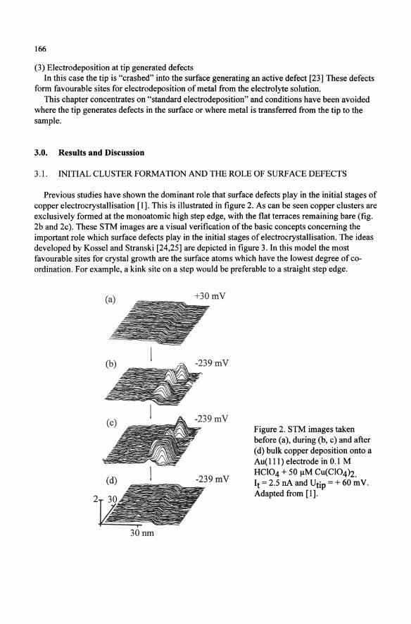
Previous studies have shown the dominant role that surface defects play in the initial stages of copper electrocrystallisation [I]. This is illustrated in figure 2. As can be seen copper clusters are exclusively formed at the monoatomic high step edge, with the flat terraces remaining bare (fig. 2b and 2c). These STM images are a visual verification of the basic concepts concerning the important role which surface defects play in the initial stages of electrocrystallisation. The ideas developed by Kossel and Stranski [24,25] are depicted in figure 3. In this model the most favourable sites for crystal growth are the surface atoms which have the lowest degree of coordination. For example, a kink site on a step would be preferable to a straight step edge.
+30mV
-239 mV
30nm
Figure 2. STM images taken before (a), during (b, c) and after (d) bulk copper deposition onto a Au(lll) electrode in 0.1 M HCl04 + 50 ~M Cu(Cl04h. It = 2.5 nA and Utip = + 60 mY. Adapted from [I].

167
Unfortunately in-situ STM has not been able to resolve individual atomic-scale kinks in step edges, presumably due to insufficient lateral resolution in the imaging of the step edges. However, there is some evidence that step edges with a higher radius of curvature ("rougher") provide a greater number of more favourable nucleation sites than relatively straight step edges. The "rougher" step edges have presumably a higher density of kink sites. Indeed, circular gold islands on the substrate surface (particularly common on Au(100)) seem to provide a particularly high density of favourable nucleation sites, presumably due to the high kink site density [3]. In such cases an effective and often continuous coverage of the rims of such gold islands is observed at a comparably early stage in the copper deposition experiment (see section 4.5).
Figure 3. "Textbook" represen~tion of the possible defect sites on an otherwise "perfect" single crystal surface. Incorporation of ad-atoms
, are shown at: A - terrace site; B - step site;
C - kink step site.
3.2. SUBSEQUENT GROWTH OF THE COPPER DEPOSIT WITHOUT ADDITIVES
A 3- dimensional growth of the copper crystallites occurs in the electrolytes without additives [1,2]. The crystallites generally have a distinctive disc shaped form as shown in figure 2. Under some circumstances the crystallites appear somewhat rounded (see for example ref. 2, fig. I), due in part to poor tip geometry and in part to over scaling in the z- direction which tends to exaggerate the effect. The scaling in the z- direction should always be carefully considered when making interpretations concerning the shape of the deposit. It is also apparent from figure 2 that the growth of the crystallites is not isometric, with the growth rates in x and y being typically significantly larger than in the z- direction.
There are essentially three growth modes which have been most thoroughly characterised for vacuum deposition and epitaxial growth on quasi-perfect (screw dislocation-free) surfaces. These are illustrated in figure 4, in accordance with the classification of Bauer [26] : a) the Volmer-Weber mechanism or the formation of bulk islands directly on-top of the substrate; (b) layer-by-Iayer or Frank-Van der Merwe growth; (c) the Stranski-Krastanov mechanism involving the deposition of one or more layers followed by the formation of 3-dimensional islands.
In-situ X-ray diffraction experiments have shown that the Au(111) surface is covered with a pseudo-morphic (lxl) Cu layer at potentials close to the Nernst potential in acidic copper electrolytes [27]. We therefore assume that the bulk copper deposition occurs on-top of the underpotentially deposited (UPD) copper monolayer. Thus the deposition of bulk copper in additive-free electrolytes can be classified as Stranski-Krastanov growth, i.e. formation of 3-dimensional clusters on-top of a monolayer deposit.

168
A B c
Figure 4. Classification of the types of growth: (a) Volmer-Weber; (b) Frank-Van der Merwe; (c) Stranski- Krastanov.
There has been much effort in developing theories to predict growth modes, particularly of physisorbed gases. In earlier models the growth mode was directly correlated with the strength of the substrate-adsorbate interactions relative to the adsorbate-adsorbate interactions. For instance, strongly attractive substrates were expected to lead to layer-by-Iayer growth (sometimes called complete wetting) while weaker ones were not (incomplete wetting). However, experiments on inert gases physisorbed on graphite produced results contrary to these predictions. This has lead more recently to the development of models including other parameters. In particular, strains in the initial layer have been identified as being crucially important in determining the growth mode. A strong substrate-adsorbate interaction can produce an internally strained first layer. In this case the energetic advantage of adsorption near to the substrate can be overwhelmed by the strain energy which would be built up by a layer-by-Iayer growth. This leads to formation of 3-dimensional crystallites on-top of the initial layer.
In the case of electrodeposition other parameters, such as solvent and electrolyte adsorption, are also known to be important. However, it has been recognised that the strains within the initial layer can also playa determining role in electrodeposition. The aforementioned ideas concerning internal strain can help us to rationalise why bulk copper deposition on gold follows a StranskiKrastanov rather than Frank-Van der Merwe growth. The first monolayer of copper on Au(lll) is epitaxially deposited due to the favourably strong copper-gold interaction. However, this first monolayer is internally strained since the Cu-Cu distance in Cu( 111) is significantly shorter (0.256 nm) than Au-Au in Au(lll) (0.289 nm). This strain is presumably a major factor which prevents the bulk copper deposition following the simple layer-by-Iayer growth.
3.3. THE INITIAL STAGES OF COPPER DEPOSITION IN THE PRESENCE OF ADDITIVES
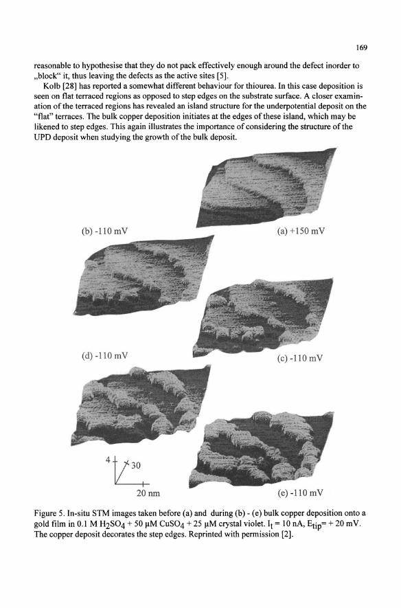
There have been several studies of the influence of additives on copper electrodeposition including crystal violet [2,3], benzotriazole derivatives (BT-B) [5] and thiourea [28]. In the case of crystal violet and benzotriazole derivatives the defects in the substrate surface are favourable sites for the nucleation of the bulk copper deposit with nucleation on flat terraced regions being generally not observed. This is illustrated in figure 5 for crystal violet addition. Deposition directly along the step edges can be seen in figures 5(b) - 5(e). It is not surprising that the surface defects remain to be the favourable nucleation sites, even with crystal violet or BT-B addition, when one compares the size of such organic molecules with the size of, for instance, an atomic scale kink in a step edge. These additives are significantly larger than such a kink and it seems
169
reasonable to hypothesise that they do not pack effectively enough around the defect inorder to "block" it, thus leaving the defects as the active sites [5].
Kolb [28] has reported a somewhat different behaviour for thiourea. In this case deposition is seen on flat terraced regions as opposed to step edges on the substrate surface. A closer examination of the terraced regions has revealed an island structure for the underpotential deposit on the "flat" terraces. The bulk copper deposition initiates at the edges of these island, which may be likened to step edges. This again illustrates the importance of considering the structure of the UPD deposit when studying the growth of the bulk deposit.
(b) -110 mV (a) + 150 mV
(d) -110 mV (c) -110mV
4ti: 20nm (e) -110 mV
Figure 5. In-situ STM images taken before (a) and during (b) - (e) bulk copper deposition onto a gold film in 0.1 M H2S04 + 50 flM CuS04 + 25 flM crystal violet. It = 10 nA, Etip= + 20 m V. The copper deposit decorates the step edges. Reprinted with permission [2] .

170
3.4. SUBSEQUENT GROWTH OF THE COPPER DEPOSIT WITH ADDITIVES
The differences between copper deposition in additive-free and additive containing electrolytes becomes first apparent when the growth of the deposit subsequent to the initial cluster formation is followed. In additive-free electrolytes the crystallites grow in 3-dimensions. However, an effective additive such as BT-B surpresses the vertical growth ofthe crystallites, so that they spread parallel to the substrate surface exhibiting quasi 2-dimensional growth. This can be seen in figure 6. The surface before bulk deposition is shown in figure 6a. Upon stepping the potential to - 400 mV copper deposition starts at the step edges (6b) and these clusters then spread laterally (6b - 6g) to produce the compact deposit seen in figure 6g. Upon stripping the deposit the original surface is revealed (6h).
+ 150mV
B
- 400 mV
- 400 mV
- 400 mV
-400 mV
- 400 mV
- 400 mV
+ 400 mV
Figure 6. In-situ STM images of copper electrodeposition on gold films from 0.1 M H2S04 + 50 11M CuS04 + 10 mgl-1 BT-B. Electrode potentials vs. Cu/Cu2+. Image (a) was taken before bulk copper deposition, images (b)-(g) during deposition and image (h) following stripping of the bulk deposit. Copyrighted and reprinted with the permission of F AMS, Inc. [29].

171
The vertical verses lateral growth of copper crystallites, in the absence of additive and with BT-B, are compared in figure 7. The height of the copper crystallites has been plotted against their average width, with the data being taken for a number of different crystallites and for various times. There is quite a large amount of scatter of the points although the general trend can be seen. In the absence of additive there is a clear 3-dimensional growth of the crystallites. This can be contrasted with a relative constant height of the copper crystallites as they laterally expand from a width of about 10 to 50 nm. So it appears that the additives are blocking the formation of new growth centres on-top of the disc shaped crystallites, and thus further promoting incorporation of the copper ad-atoms at the edges of the discs.
10 D 0 0 0
0
9 0 o (A) 0
8 0
7 Q 0
E 6 0 0
~ 1: 5 00
00
'" 0 0 0
-; 4 00 0
:I: 'I> 0 0 0 0
3 0 0 0 0
8 o go 2 0 0
o 00 o · 0 ~ o • • • • • . , · 0 •• • •
0
0 10 20 30 40 50 60
Wldth/nm
Figure 7. The electrolytic growth of copper microcrystallites on gold films in 0.1 M H2S04 + 10 mM CuS04 in the absence (A) and presence of BT-B (B). The height of individual clusters is plotted against their average width (see text).
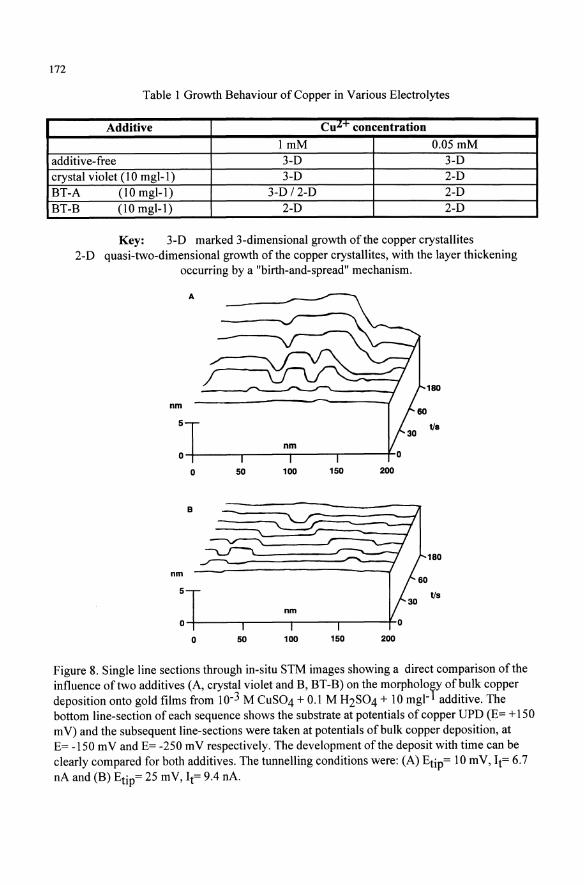
Some additives are more effective at surpressing the vertical propagation of the copper crystallites in favour of their lateral spreading. For instance crystal violet only effectively surpresses the. vertical growth ~or slow growth rates. fro~ very dil~te copper electro~tes. BT-B IS more effective than crystal VIOlet and the companson IS shown In figure 8 for 10- M CuS04 + 0.1 M H2S04 + either (A) crystal violet or (B) 10 mgl- I BT -B. This figure shows a single cross-sections through a given section of the surface and illustrates the development of the deposit with time.
The growth morphology of the copper deposit is compared for various additive types and two different copper concentrations in table I . 2-dimensional copper crystallite growth is observed for BT-B at both copper concentrations and for crystal violet only at lower copper concentrations. At the lower copper concentration the BT-A additive also promotes lateral spreading of the copper deposit, while at the higher copper concentration a mixed behaviour is observed, with a proportion of the crystallites exhibiting a 2-dimensional growth and a proportion showing a marked 3D growth. On the basis of these observations the additives can be ranked in terms of their ability to surpress the vertical growth of copper crystallites:
BT-B > BT-A > Crystal Violet » HS04- (additive-free)
172
Table 1 Growth Behaviour of Copper in Various Electrolytes
Additive Cu:L+ concentration
lmM 0.05 mM additive-free 3-D 3-D crystal violet (10 mgl-l) 3-D 2-D BT-A (10 mgl-l) 3-D / 2-D 2-D BT-B (10 mgl-l) 2-D 2-D
Key: 3-D marked 3-dimensional growth of the copper crystallites 2-D quasi-two-dimensional growth ofthe copper crystallites, with the layer thickening
occurring by a "birth-and-spread" mechanism.
A
180
nm
5 tis
o~----~~----~----~------~
o 50 100 150 200
B
180
nm
5 tis
o~------~----~----~------~
o 50 100 150 200
Figure 8. Single line sections through in-situ STM images showing a direct comparison of the influence of two additives (A, crystal violet and B, BT-B) on the morphology of bulk copper deposition onto gold films from 10-3 M CuS04 + 0.1 M H2S04 + 10 mgl- l additive. The bottom line-section of each sequence shows the substrate at potentials of copper UPD (E= + 150 m V) and the subsequent line-sections were taken at potentials of bulk copper deposition, at E= -150 mV and E= -250 mV respectively. The development of the deposit with time can be clearly compared for both additives. The tunnelling conditions were: (A) Etip= 10 mY, It= 6.7 nA and (B) Etip= 25 mY, It= 9.4 nA.
173
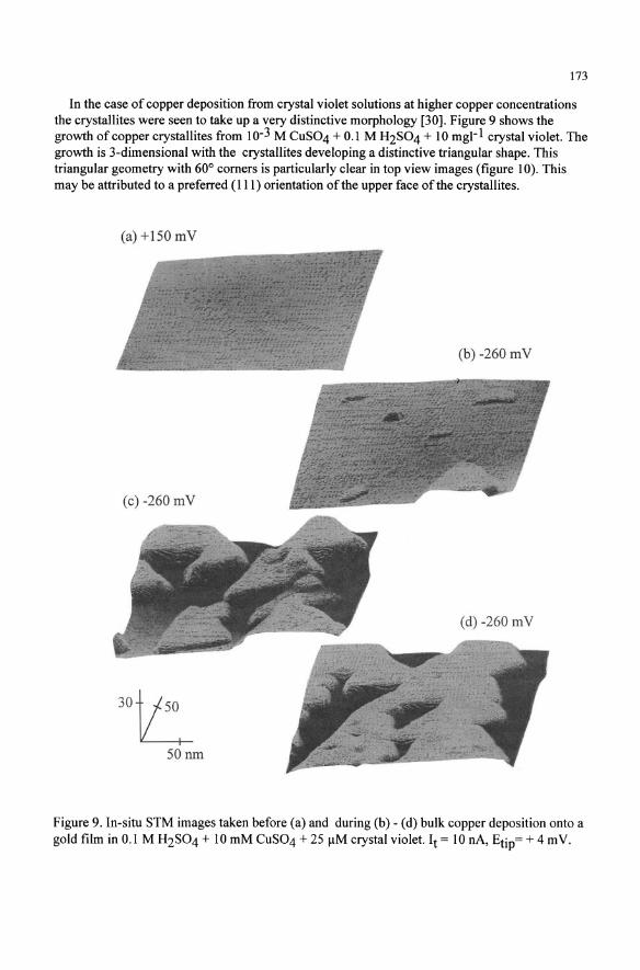
In the case of copper deposition from crystal violet solutions at higher copper concentrations the crystallites were seen to take up a very distinctive morphology [30]. Figure 9 shows the growth of copper crystallites from 10-3 M CuS04 + 0.1 M H2S04 + 10 mgl- I crystal violet. The growth is 3-dimensional with the crystallites developing a distinctive triangular shape. This triangular geometry with 60° comers is particularly clear in top view images (figure 10). This may be attributed to a preferred (III) orientation of the upper face of the crystallites.
(a) +150 mY
(b) -260 mY
(c) -260 mY
30t[: 50nm
Figure 9. In-situ STM images taken before (a) and during (b) - (d) bulk copper deposition onto a gold film in 0.1 M H2S04 + 10 mM CuS04 + 25 11M crystal violet. It = 10 nA, Etip= + 4 mY.

174
nil
Figure 10. A topview representation of figure 9c.
3.5. RIM FORMATION AT Au(IOO) ISLANDS
A rather interesting phenomenon has been observed for the initial stages of copper deposition on Au(IOO) surfaces [3]. This has been described as the "rim effect". This observation is described here, since a rather similar effect is one of the main mechanistic routes leading to the formation of subsequent layers in the layer-by-Iayer growth (see next section).
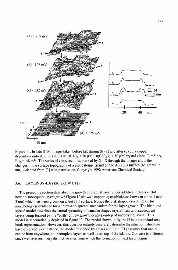
The unreconstructed Au( 1 00) surface has a rather distinctive topography. The freshly prepared surface possesses a hexagonal structure which has a higher density of surface atoms (ca. 20 %) than the unreconstructed (IxI) surface. Unless certain precautions are taken the hexagonaJly structured surface is converted into the unreconstructed surface upon immersion in the electrolyte. This hexagonal to (1 xl) transition results in an excess of surface gold atoms. These surface atoms coalesce by means of surface diffusion to form monoatomic high gold islands, which range in diameter from typically several nanometers up to about 30 nm [3]. Such a surface is shown in figure 11 a.
The edges of the gold islands on the Au(IOO) surface are favourable nucleation sites for copper deposition. This is seen in figures 11 band 11 c. Notice how the copper deposit forms an almost continuous rim around the edges of the gold islands. The formation ofa rim right around the step edge can be particularly clearly seen in cross-sections through the islands (figure 11). Upon stepping the potential positive the rim is stripped (fig. lId).
175
(a) + 259 mY
a
d
20 40 nm
10 nm
Figure 11. In-situ STM images taken before (a), during (b - c) and after (d) bulk copper deposition onto Au(100) in 0.1 M HCl04 + 50 JlM Cu(Cl04)2 + 10 JlM crystal violet. It = 5 nA, Etip= -48 m V. The series of cross sections, marked by X - X through the images show the changes in the surface topography of a monoatomic island on the Au(100) surface (height = 0.2 nm). Adapted from [3] with permission. Copyright 1992 American Chemical Society.
3.6. LAYER-BY-LAYERGROWTH[5]
The preceding section described the growth of the first layer under additive influence. But how do subsequent layers grow? Figure 12 shows a copper layer (thickness between about 1 and 3 nm) which has been grown on a Au( Ill) surface. Notice the disk shaped crystallites. This morphology is evidence for a "birth-and-spread" mechanism for the layer growth. The birth-andspread model describes the lateral spreading of pancake shaped crystallites, with subsequent layers being formed by the "birth" of new growth centres on-top of underlying layers. This model is schematically depicted in figure 13. The model shown in figure 13 is the standard text book representation. However, this does not entirely accurately describe the situation which we have observed. For instance, the model described by Ohara and Reid [31] assumes that nuclei can be born anywhere, on incomplete layers as well as on-top of the islands. Our case is different since we have seen very distinctive sites from which the formation of next layer begins.

176
nm
2
Figure 12. An in-situ STM image of copper (thickness between about 1 - 3 nm) deposited at -300 mY on a Au(lll) film from 10-3 M CuS04 + 0.1 M H2S04 + 10 mgl-1 BT-B. A number of monoatomic high pancake-shaped copper crystallites can be seen and this indicates a birthand-spread growth mechanism for layer thickening. Reprinted with permission from [5].
Figure 13. A schematic representation of the birth-and-spread model. This is the conventional representation. A somewhat modified version is proposed in the text.
177
The various types of sites which have been observed for the "birth" of subsequent layers are schematically shown in figure 14 as cross-sections. Figure 14a shows a new growth centre being formed at the meeting point of two disc shaped crystallites which grow together. Figure 14b depicts the growth of the next layer inwards fromthe upper edge of the disc shaped crystallite. In effect the next layer grows from a rim which forms at the edge of the disc crystallite. Comparisons may be made with the "rim effect" seen on Au(lOO) substrates. In fact mechanisms A and B are rather similar and should maybe be considered as just one, since formation of the new layer starts from the edges of the copper discs in both cases. Figure 14c shows another possible mechanism, in which a new growth centre is formed at a defect site on-top of a disc crystallite. Experimentally we have observed that Mechanisms AlB are more prevalent then mechanism C, at least in the case of slow electrocrystallization under the influence of an effective additive such as BT-B.
A. KEY:
~ Substrate
B. First Cu layer - Subsequent Cu layers
C. \ Defect
Figure 14. Possible sites for the development of subsequent copper layers
The fo~ma~ion of a subs~quent laJer can be seen in figure 15. This sequence of imayes was recorded In-SItu by STM WIth a 10- M CuS04 electrolyte + 0.1 M H2S04 + 10 mgl- BT-B. Figure 15 (a) shows the gold surface prior to bulk copper deposition. Upon stepping the potential to -400 mV a number of copper crystallites were formed at surface defects (fig. 15b) and these then proceeded to spread laterally to form the first bulk layer. The formation of a second layer can be seen in images (e) and (f). Notice how the second layer begins at the rim of the underlying copper disc. The second layer then proceeds to spread further on-top of the copper disc. This growth behaviour clearly corresponds to mechanism B.
3.7. SUBSTRATE INFLUENCE
Another interesting feature arises from figure 15, for the deposition of copper layers in the presence of additives. The first complete copper layer has a height considerably thicker than one monolayer (fig. 15 c-e), while further copper layers are generally monoatomic in height. The first copper layer typically reaches a thickness of up to 4-7 monolayers (fig. 15f). A schematic representation of the deposition of copper on Au(lll) is shown in figure 16. We have called this growth behaviour a "quasi layer-by-layer" growth. [2,5]
178
60 nm
60 nm
Figure IS. A sequence of in-situ STM images showing copper deposition from 10-3 M CuS04 + 0.1 M H2S04 + 10 mgl- l BT-B. Image (a) shows the surface prior to bulk copper deposition (+ ISO m V) and (b) - (f) show the gradual development of the first bulk copper layer following a potential step to - 400 m V. The growth of a copper "multi"- layer, with a lateral spreading of the crystallites, can be seen in figures (b) to (d). The development of a monoatomic high further layer can be seen in figure (e) and (f) and is marked by arrows. The tunnelling current was 9 nA and the tip potential 25 mY. Reproduced with permission from [5].
179
This difference between the deposition of the first and subsequent layers is consistently observed and indicates a pronounced influence of the gold substrate. The first bulk copper layer is deposited onto the Au(1ll) substrate surface covered with a UPD copper layer. Since the CuCu distance in Cu(11l) is significantly shorter (0.256 nm) than the Au-Au distance in bulk Au(1ll) (0.289 nm) we may expect this interface to be considerably strained. We have hypothesised that this strain may be better relieved by the growth of a "multi-layer" rather than a monolayer at this stage of the deposition [5] . The assumption is that the multi-layer is more able to "deal with" the interfacial strains by distributing them more evenly through-out a thicker layer. Analogies may be made with the strain which leads to the Stranski Krastanov growth in the absence of additives. The situation is different for subsequent bulk layers where the copper is deposited onto a underlying surface which presumably possesses Cu-Cu distances closer to those of a Cu(111) surface.
W@$'~~AU(1 1 1)
f UPDCu
i@dPrkdbPdt'yJ (monolayer)
Not observed
First bulk Cu layer (mono-layer)
Subsequent Cu (mono)-Iayers
quasl- layer-by-Iayer growth
First bulk Cu layer ('multi-layer")
Figure 16. A schematic representation of the "quasi layer-by-layer" growth observed for copper deposition on Au(lI1) from acidic copper electrolytes with an effective additive.
An alternative explanation for the difference between the first and subsequent bulk layers is that the critical copper nuclei, which are formed on the substrate surface may themselves have a height of several monolayers. A nucleus would then proceed to grow laterally as a layer thicker than a single monolayer. Indeed the critical nuclei itself may be a "3-dimensional" cluster of copper atoms with a height equivalent to several monolayers (as opposed to being a 2-dimensional nucleus). However, it should be noted that the copper deposition experiments were carried out at relatively high overpotentials, where the nuclei probably consists of only a few atoms (not more than 10) [32,33] . The formation of subsequent layers is a rather different situation since this involves deposition of copper onto a template which has characteristics presumably much closer to those of a "copper surface" (i.e. this situation is not nucleation onto a foreign substrate).
180
3.8. ELECTRODEPOSITION ONTO CONDUCTIVE POLYMERS
The initial stages of copper deposition onto intrinsically conductive polypyrrole films have also been examined [6]. Figure 17 shows in-situ AFM images of copper electrodeposition onto polypyrrole from 0.1 M H2S04 + 1 mM CuS04. The polypyrrole surface prior to copper electrodeposition is shown in figure 17a. The same area of the surface has been imaged following a potential step to -150 m V (figure 17b). Copper clusters can be clearly seen on the surface and these have been observed to grow in 3-dimensions [6].
Copper deposition on polypyrrole has also been examined with the addition ofBT-B. However, the BT-B additive has no marked effect on the..growth of copper on polypyrrole and this clearly contrasts with the results obtained for gold substrates. The comparison between the results obtained for gold and polypyrrole substrates are summarised in table 2.
It seems rather unlikely that copper layers are deposited onto polypyrrole before formation of the bulk copper deposit. Formation of3-D islands directly on-top of the substrate corresponds to the Volmer-Weber mode of growth. The Volmer-Weber growth mode predominates for weakly attractive substrates, i.e. situations where the deposit to substrate interaction is relatively weak in comparison to the deposit-deposit interaction. It may also be the case that the additive is poorly adsorbed on the polypyrrole substrate, and hence unable to influence the deposition process.
E c
o o r--
Figure 17. In-situ AFM images of conductive polypyrrole taken before (a, + 30 mV) and immediately following a potential step to -ISO m V (b). The electrolyte was 0.1 M H2S04 + I mM CuS04.

Table 2. Summary of Observations for Bulk Copper Deposition onto Gold and Polypyrrole Electrodes
Base electrolyte: 0.1 M H2S04 + 1 mM CuS04
181
Substrate Additive Growth Morphology Growth Mechanism
Key:
Gold Gold
Polypyrrole Polypyrrole
2-D 3-D
Summary
None 3-D Stranski-Krastanov BT-B 2-D Frank-Van der Merwe None 3-D Volmer-Weber BT-B 3-D Volmer-Weber
quasi- 2- dimensional growth of bulk copper islands 3- dimensional growth of bulk copper islands
In-situ scanning probe microscopies provide new possibilities for studying the initial stages of bulk metal deposition processes with an unprecedented resolution. This article has illustrated this with the example of copper electrodeposition onto well defined gold substrates.
The deposition of copper begins at defects in the substrate surface, such as steps edges. Additives such as crystal violet and BT- derivatives do not block these defects from being the favourable nucleation sites. In the absence of additives the micro- crystallites grow in 3-dimensions and are characterised by a disc shaped form.
Stranski-Krastanov growth has been observed for copper deposition on Au(111) in the absence of additives. The strong copper-gold interaction leads to the deposition of a monolayer of copper at underpotentials and to a significant mis-match between the copper monolayer and the bulk deposit. This mis-match is the most likely reason for the quenching of the epitaxial growth, since a high strain energy would presumably result in such films. Effective additives such as BT-B have a pronounced effect on the growth of the copper electrodeposit. In this case a quasi layer-by-Iayer growth is observed. A pronounced difference is seen between the deposition of the first bulk copper layer and subsequent layers. The first bulk copper layer grows as a "multi-layer" up to a height of about 7 monolayers. However, subsequent layers grow as monolayers (Frank-Van der Merwe growth). This difference between the first and subsequent layers also presumably results from the mis-match. The most common sites for the formation of the subsequent layers are the edges of the rims of the underlying disc shaped crystallites.
Finally, the initial stages of copper electrodeposition on polypyrrole were observed in-situ with AFM. The growth of copper on this substrate is similar in the presence and absence of additives. In both cases 3-dimensional copper islands are observed. This is the Volmer-Weber mode of growth.
Acknowledgements
It is a pleasure to thank my colleagues with whom I have co-operated in this area: C. Bach, Dr. N. Batina, Dr. H. Meyer and Profs. D.M. Kolb and R.J. Behm.
182
References
[1] RJ. Nichols, D.M. Kolb and RJ. Behm, J.Electroanal. Chern., 313 (1991) 109. [2] RJ. Nichols, W. Beckmann, H. Meyer, N. Batina and D.M. Kolb, J. Electroanal. Chern.,
330 (1992) 381. [3] N. Batina, D.M. Kolb and RJ. Nichols, Langmuir, 8 (1992) 2572. [4] D.M. Kolb, RJ. Nichols and RJ. Behm, in: Electrified Interfaces in Physics, Chemistry
and Biology, Ed. R Guidelli, NATO ASI Series C (Kluwer, Dordrecht, 1992), p. 275. [5] RJ. Nichols, C.E. Bach, H. Meyer, Ber. Bunsenges. Phys. Chern. 97 (1993) No.8, 1012. [6] RJ. Nichols, D. Schroer, G. Urrutia and H. Meyer, The Electrochemical Society,
Proceedings of the Fourth Syposium on Metallized Plastics, in press, 1994 [7] R Sonnenfeld and P.K. Hansma, Science, 232 (1986) 211. [8] T.R.!. Cataldi, I.G. Blackham, GAD. Briggs, lB. Pethica and HAO. Hill,
J. Electroanal. Chern., 290 (1990) 1. [9] S.-L. Yau, C.M. Vitus and B. Schardt, J. Am. Chern. Soc., 112 (1990) 3677. [10] H. Siegenthaler and R Christoph, in: Scanning Tunneling Microscopy and Related
Methods, Eds. RJ. Behm, N. Garcia and H. Rohrer, Nato ASI Series E184 (1990) 315. [11] R Sonnenfeld and B.C. Schardt, Appl. Phys. Lett., 49 (1986) 1172. [12] K.ltaya and S. Sugawara, Chern. Lett., (1987) 1927. [13] J. Schneir, V. Elings and P.K. Hansma, J. Electrochem. Soc., 135 (1988) 2774. [14] MJ. Armstrong and RH. Muller, J. Electrochem. Soc., 138 (1991) 2303. [15] R Christoph, H.Siegenthaler, H.Rohrer and H.Wiese, Electrochim. Acta, 34 (1989) 1011 [16] K. Itaya and E. Tomita, Surf. Sci., 201 (1988) L507. [17] RS. Robinson, J. Electroanal. Chern., 136 (1989) 584. [18] K. Uosaki and H. Kita, J. Vac. Sci. Technol. A8 (1990) 520. [19] X. Zhang and U. Stimming, J. Electroanal. Chern., 291 (1990) 273. [20] D.M. Kolb. N. Batina and T. Will, Disc. Faraday Soc. No. 94 on "The Liquid/Solid
Interface at High Resolution", Newcastle, 1992. [21] C.E. Bach, RJ. Nichols, W. Beckmann, H. Meyer, A. Schulte, J.O. Besenhard and P.D.
Jannakoudakis, 1 Electrochem. Soc., 140 (1993) 1281. [22] R Ullmann, T. Will and D.M. Kolb, Chern. Phys. Lett., Vol. 209 (1993) 238. [23] W. Li, JA Virtanen and RM. Penner, Appl. Phy. Lett., 60 (1992) 1181. [24] H. Fischer, "Electrolytischer Abscheidung und Electrokristallisation von Metallen",
Springer Verlag 1954. [25] LN. Stranski, Z. Phys. Chern., 136, (1928) 259. [26] E. Bauer, Z. Kristallogr., 110 (1958) 372. [27] O.R Melroy, M.G. Samant, G.L. Borges, lG. Gordon, L. Blum, lH. White, MJ.
Albarelli, M. McMillan, H.D. Abruiia, Langmuir, 4 (1988) 728. [28] D.M. Kolb, Extended Abstracts for the Electrochemical Society Meeting, 1993, Vol. 93-
1, Honolulu, Abs. No. 1933. [29] RJ. Nichols, D. Schroer and H. Meyer, Scanning, 15 (1993) 266. [30] RNichols, E.Bunge and H.Meyer, IUVSTA Workshop Poster, San Benedetto,ltaly 1994. [31] M. Ohara and R Reid, "Modeling crystal growth rates from solution", Prentice-Hall
International, London, 1973. [32] I. Markov and S. Stoyanov, Contemp. Phys., Vol. 28 No.3 (1987) 267. [33] I. Markov and R. Kaischew, Thin Solid Films, 32 (1976) 163.