SCANNING PROBE MICROSCOPE TECHNIQUES, SPM SCANNING...
23
SCANNING PROBE MICROSCOPE TECHNIQUES, SPM SCANNING TUNNELLING MICROSCOPE, STM and ATOMIC FORCE MICROSCOPE, AFM
Transcript of SCANNING PROBE MICROSCOPE TECHNIQUES, SPM SCANNING...

SCANNING PROBE MICROSCOPE TECHNIQUES, SPM
SCANNING TUNNELLING MICROSCOPE, STM and
ATOMIC FORCE MICROSCOPE, AFM

Scanning probe microscopes (SPMs) are a family of instruments used for studying surface properties of materials on the atomic level.
A fine probe is scanned over a surface (or the surface is scanned under the probe). By using such a probe, researchers are no longer restrained by the wavelength of light or electrons. The resolution obtainable with this technique can resolve atoms ; typ. ~ 20 Å in x,y directions (ideal sample & instruments 1 Å), in z direction 1 Å, where electron mic. ~ 50 Å. Unlike optical and electron microscopes SPMs details not only on x,y axis but also on the z axis.
True 3-D maps of surfaces are possible.


The three most common scanning probe techniques are: Atomic Force Microscopy (AFM) measures the interaction force between the tip and surface. The tip may be dragged across the surface, or may vibrate as it moves. The interaction force will depend on the nature of the sample, the probe tip and the distance between them. Scanning Tunneling Microscopy (STM) measures a weak electrical current flowing between tip and sample as they are held a very distance apart. Near-Field Scanning Optical Microscopy (NSOM) scans a very small light source very close to the sample. Detection of this light energy forms the image. NSOM can provide resolution below that of the conventional light microscope.

Scanning Tunneling Microscopy
The scanning tunneling microscope (STM) is the ancestor of all scanning probe microscopes. It was invented in 1981 by Gerd Binnig and Heinrich Rohrer at IBM Zurich. Five years later (1986) they were awarded the Nobel prize in physics for its invention. The first instrument to generate real-space images of surfaces with atomic resolution.
Based on quantum mechanical tunneling current Works for electrically conductive samples!! Imaging, spectroscopy and manipulation possible
Scanning sample in an x/y raster pattern with a very sharp tip that moves up and down along the z axis as the surface topography changes . This movement is measured and translated by a computer into an image of the surface topography.( often on atomic size scale)

STMs use a sharpened, conducting tip with a bias voltage applied between the tip and the sample. When the tip is brought within about 10 Å of the sample, electrons from the sample begin to “tunnel” through the 10 Å gap into the tip or vice versa, depending upon the sign of the bias voltage.
• Piezoelectric materials are ceramics that change dimensions in response to an applied voltage.

This is a macro scale image of an etched tungsten scanning tunnelling microscopy (STM) tip. The ridges below etched region are the result of the die used in the extruding process. Uniform geometry contributes to a more stable tip.
Simply by cutting a thin metal wire with a wire cutter. There is always a single atom left over at the very top.
Stm tip conductive Pt/Ir

The resulting tunneling current varies with tip-to-sample spacing, and it is the signal used to create an STM image. For tunneling to take place, both the sample and the tip must be conductors or semiconductors.
Tunneling current
A current passes through a medium that contains no electrons; a vacuum
Classically, when an object hits a potential that it doesn’t have enough energy to pass, it will never go though that potential wall, it always bounces back. if you throw a ball at a wall, it will bounce back at you.
In quantum mechanics when a particle hits a potential that it doesn’t have enough energy to pass, when inside the square well, the wave function dies off exponentially. If the well is short enough, there will be a noticeable probability of finding the particle on the other side.

In a metal, the energy levels of the electrons are filled up to a particular energy, known as the ‘Fermi energy’ EF. In order for an electron to leave the metal, it needs an additional amount of energy Φ, the so-called ‘work function’.
When the specimen and the tip are brought close to each other, there is only a narrow region of empty space left between them. On either side, the electrons are present up to the Fermi energy. They need to overcome a barrier Φ to travel from tip to specimen or vice versa.
If the distance d between specimen and tip is small enough, electrons can ‘tunnel’ through the vacuum barrier. When a voltage V is applied between specimen and tip, the tunneling effect results in a net electron current. In this example from specimen to tip. This is the tunneling current.

The tunneling current is an exponential function of distance; if the separation between the tip and the sample changes by 10% (on the order of 1Å), the tunneling current increases by a factor of 10. This exponential dependence gives STMs their remarkable sensitivity. STMs can image the surface of the sample with sub-angstrom precision vertically, and atomic resolution laterally.
• Probe the local electronic structure of a sample’s surface
It α e-2αs

STMs can be designed to scan a sample in either of two modes: Constant-height Mode
Constant-current Mode
The tip travels in a horizontal plane above the sample The tunneling current varies depending on topography and the local surface electronic properties of the sample. The tunneling current measured at each location on the sample surface constitute the data set, the topographic image.
STMs use feedback to keep the tunneling current constant by adjusting the height of the scanner at each measurement point. For example, when the system detects an increase in tunneling current, it adjusts the voltage applied to the piezoelectric scanner to increase the distance between the tip and the sample.
Atomically flat surfaces as otherwise a tip crash would be inevitable. One of its advantages is that it can be used at high scanning frequencies

Atomic Force Microscopy
Probes the surface of a sample with a sharp tip, a couple of microns long and often less than 100Å in diameter. (The tip is located at the free end of a cantilever that is 100 to 200μm long)
AFMs can be used to study insulators and semiconductors as well as electrical conductors.
Forces between the tip and the sample surface cause the cantilever to bend or deflect A detector measures the cantilever deflection as the tip is scanned over the sample, or the sample is scanned under the tip. The measured cantilever deflections allow a computer to generate a map of surface topography
3-D Surface Topography Force Measurements in pico-Newton - nano-Newton range
As in STM motion of the tip or sometimes the sample,is achieved with a piezoelectric tube.
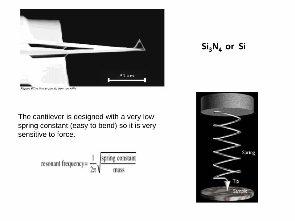
Si3N4 or Si
The cantilever is designed with a very low spring constant (easy to bend) so it is very sensitive to force.

A diode laser is focused onto the back of a reflective cantilever. As the tip scans the surface of the sample, moving up and down with the contour of the surface, the laser beam is deflected off the attached cantilever into a photodiode.
Up and down movement of tip recorded by position sensing photodiode ((dual element photodiode that measures differences in light intensity and converts to voltage)

Several forces typically contribute to the deflection of an AFM cantilever. The force most commonly associated with atomic force microscopy is an interatomic force called the van der Waals force.
van der Waals force curve
At the right side of the curve, the atoms are separated by a large distance. As the atoms are gradually brought together, they first weakly attract each other.
This attraction increases until the atoms are so close together that their electron clouds begin to repel each other electrostatically. This electrostatic repulsion progressively weakens the attractive force as the distance continues to decrease. Following the graph, the force goes to zero when the distance reaches a couple of angstroms
Anything closer than this, the total van der Waals force becomes positive (repulsive). This distance will not change, therefore any more attempt to force the sample and tip closer will result in deformation or damage to the sample or the tip.

The in-plane resolution depends on the geometry of the probe. In general, the sharper the probe is the higher the resolution of the AFM image.
Fig. The image on the right will have a higher resolution because the probe used for the measurement is much sharper.
a sharp probe a dull probe

Modes of operation
Contact Mode
In contact-mode the tip either scans at ; constant small height above the surface constant force In the constant height mode the height of the tip is fixed, whereas in the constant-force mode the deflection of the cantilever is fixed and the motion of the scanner in z-direction is recorded. By using contact-mode AFM, even “atomic resolution” images are obtained.
the tip makes soft “physical contact” with the surface of the sample
The deflection of the cantilever Dx is proportional to the force acting on the tip, via Hook’s law, F=-k. x, where k is the spring constant of the cantilever.
Contact mode operates in the repulsive regime of the van der Waals curve

it is necessary to have a cantilever which is soft enough to be deflected by very small forces and has a high enough resonant frequency to not be susceptible to vibrational instabilities. Silicon Nitride tips are used for contact mode.
In this mode, the probe operates in the attractive force region and the tip-sample interaction is minimized. The use of non-contact mode allowed scanning without influencing the shape of the sample by the tip-sample forces. In most cases, the cantilever of choice for this mode is the one having high spring constant of 20- 100 N/m so that it does not stick to the sample surface at small amplitudes. The tips mainly used for this mode are silicon probes.
Non Contact Mode
Advantages over contact: no lateral forces, non destructive/no contamination to sample, etc.

Contact Mode AFM Advantages: - High scan speeds. - “Atomic resolution” is possible. - Easier scanning of rough samples with extreme changes in vertical topography. Disadvantages: - Lateral forces can distort the image. - Capillary forces from a fluid layer can cause large forces normal to the tipsample interaction. - Combination of these forces reduces spatial resolution and can cause damage to soft samples.
Non-contact Mode AFM Advantage: - Low force is exerted on the sample surface and no damage is caused to soft samples Disadvantages: - Lower lateral resolution, limited by tip-sample separation. - Slower scan speed to avoid contact with fluid layer. - Usually only applicable in extremely hydrophobic samples with a minimal fluid layer.

Tapping Mode (intermittent contact Mode)
The cantilever in an AFM can be vibrated using a piezoelectric ceramic. The cantilever is oscillated close to its resonance frequency.( a few hundred kilohertz) The oscillation is driven by a constant driving force and the amplitude is monitored continuously. When the vibrating cantilever comes close to a surface, the amplitude and phase of the vibrating cantilever may change. An electronic feedback loop ensures that the oscillation amplitude remains
constant, such that a constant tip-sample interaction is maintained during scanning.
In ambient conditions, most samples develop a liquid meniscus layer. Because of this, keeping the probe tip close enough to the sample for short-range forces to become detectable while preventing the tip from sticking to the surface presents a major problem for non-contact dynamic mode in ambient conditions. Dynamic contact mode (also called intermittent contact or tapping mode) was developed to bypass this problem.
In this mode, tip contacts the surface for only a brief time periodically , then removed.
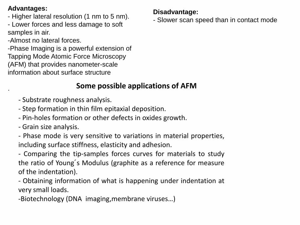
Advantages: - Higher lateral resolution (1 nm to 5 nm). - Lower forces and less damage to soft samples in air. -Almost no lateral forces. -Phase Imaging is a powerful extension of Tapping Mode Atomic Force Microscopy (AFM) that provides nanometer-scale information about surface structure .
- Substrate roughness analysis. - Step formation in thin film epitaxial deposition. - Pin-holes formation or other defects in oxides growth. - Grain size analysis. - Phase mode is very sensitive to variations in material properties, including surface stiffness, elasticity and adhesion. - Comparing the tip-samples forces curves for materials to study the ratio of Young´s Modulus (graphite as a reference for measure of the indentation). - Obtaining information of what is happening under indentation at very small loads. -Biotechnology (DNA imaging,membrane viruses…)
Disadvantage: - Slower scan speed than in contact mode
Some possible applications of AFM

Multimode SPM