Scalable Production of Boron Quantum Dots for Broadband ...
10
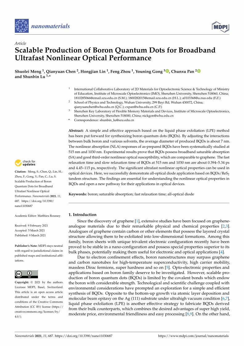
nanomaterials Article Scalable Production of Boron Quantum Dots for Broadband Ultrafast Nonlinear Optical Performance Shuolei Meng 1 , Qianyuan Chen 2 , Hongjian Lin 1 , Feng Zhou 1 , Youning Gong 3 , Chunxu Pan 2 and Shunbin Lu 1, * Citation: Meng, S.; Chen, Q.; Lin, H.; Zhou, F.; Gong, Y.; Pan, C.; Lu, S. Scalable Production of Boron Quantum Dots for Broadband Ultrafast Nonlinear Optical Performance. Nanomaterials 2021, 11, 687. https://doi.org/10.3390/ nano11030687 Academic Editor: Matthieu Roussey Received: 9 February 2021 Accepted: 5 March 2021 Published: 9 March 2021 Publisher’s Note: MDPI stays neutral with regard to jurisdictional claims in published maps and institutional affil- iations. Copyright: © 2021 by the authors. Licensee MDPI, Basel, Switzerland. This article is an open access article distributed under the terms and conditions of the Creative Commons Attribution (CC BY) license (https:// creativecommons.org/licenses/by/ 4.0/). 1 International Collaborative Laboratory of 2D Materials for Optoelectronic Science & Technology of Ministry of Education, Institute of Microscale Optoelectronics (IMO), Shenzhen University, Shenzhen 518060, China; [email protected] (S.M.); [email protected] (H.L.); [email protected] (F.Z.) 2 School of Physics and Technology, Wuhan University, 299 Bayi Rd, Wuhan 430072, China; [email protected] (Q.C.); [email protected] (C.P.) 3 Shenzhen Key Laboratory of Flexible Memory Materials and Devices, Institute of Microscale Optoelectronics, Shenzhen University, Shenzhen 518000, China; [email protected] * Correspondence: [email protected] Abstract: A simple and effective approach based on the liquid phase exfoliation (LPE) method has been put forward for synthesizing boron quantum dots (BQDs). By adjusting the interactions between bulk boron and various solvents, the average diameter of produced BQDs is about 7 nm. The nonlinear absorption (NLA) responses of as-prepared BQDs have been systematically studied at 515 nm and 1030 nm. Experimental results prove that BQDs possess broadband saturable absorption (SA) and good third-order nonlinear optical susceptibility, which are comparable to graphene. The fast relaxation time and slow relaxation time of BQDs at 515 nm and 1030 nm are about 0.394–5.34 ps and 4.45–115 ps, respectively. The significant ultrafast nonlinear optical properties can be used in optical devices. Here, we successfully demonstrate all-optical diode application based on BQDs/ReS 2 tandem structure. The findings are essential for understanding the nonlinear optical properties in BQDs and open a new pathway for their applications in optical devices. Keywords: boron; saturable absorption; fast relaxation time; all-optical diode 1. Introduction Since the discovery of graphene [1], extensive studies have been focused on graphene- analogue materials due to their remarkable physical and chemical properties [2,3]. Analogues of graphene contain carbon or other elements that possess the layered crystal structure allowing them to be exfoliated into low-dimensional formations. Among this family, boron sheets with unique trivalent electronic configuration recently have been proved to be stable in a nano-configuration and possess special properties superior to its bulk phases, potentially making them useful for electronic and optical applications [4]. Due to electron confinement effects, boron nanostructures may surpass graphene and carbon nanotubes for high-temperature superconductivity, high carrier mobility, massless Dirac fermions, super hardness and so on [5]. Opto-electronic properties and applications based on boron family deserve to be investigated. However, scalable pro- duction of boron quantum dots (BQDs) is limited by the covalent bonds which endow the boron with considerable strength. Technological and scientific challenge coupled with environmental considerations have prompted an exploration for a simple and efficient synthesis of BQDs. Opposite to the bottom-up growth via atomic layer deposition and molecular beam epitaxy on the Ag (111) substrate under ultrahigh vacuum condition [6,7], liquid phase exfoliation (LPE) is another effective strategy to fabricate BQDs derived from their bulk counterparts, which combines the desired advantages of super high yield, moderate price, environmental friendliness and easy processing [8,9]. On the other hand, Nanomaterials 2021, 11, 687. https://doi.org/10.3390/nano11030687 https://www.mdpi.com/journal/nanomaterials
Transcript of Scalable Production of Boron Quantum Dots for Broadband ...
nanomaterials
Article
Scalable Production of Boron Quantum Dots for BroadbandUltrafast Nonlinear Optical Performance
Shuolei Meng 1, Qianyuan Chen 2, Hongjian Lin 1, Feng Zhou 1, Youning Gong 3 , Chunxu Pan 2
and Shunbin Lu 1,*
�����������������
Citation: Meng, S.; Chen, Q.; Lin, H.;
Zhou, F.; Gong, Y.; Pan, C.; Lu, S.
Scalable Production of Boron
Quantum Dots for Broadband
Ultrafast Nonlinear Optical
Performance. Nanomaterials 2021, 11,
687. https://doi.org/10.3390/
nano11030687
Academic Editor: Matthieu Roussey
Received: 9 February 2021
Accepted: 5 March 2021
Published: 9 March 2021
Publisher’s Note: MDPI stays neutral
with regard to jurisdictional claims in
published maps and institutional affil-
iations.
Copyright: © 2021 by the authors.
Licensee MDPI, Basel, Switzerland.
This article is an open access article
distributed under the terms and
conditions of the Creative Commons
Attribution (CC BY) license (https://
creativecommons.org/licenses/by/
4.0/).
1 International Collaborative Laboratory of 2D Materials for Optoelectronic Science & Technology of Ministryof Education, Institute of Microscale Optoelectronics (IMO), Shenzhen University, Shenzhen 518060, China;[email protected] (S.M.); [email protected] (H.L.); [email protected] (F.Z.)
2 School of Physics and Technology, Wuhan University, 299 Bayi Rd, Wuhan 430072, China;[email protected] (Q.C.); [email protected] (C.P.)
3 Shenzhen Key Laboratory of Flexible Memory Materials and Devices, Institute of Microscale Optoelectronics,Shenzhen University, Shenzhen 518000, China; [email protected]
* Correspondence: [email protected]
Abstract: A simple and effective approach based on the liquid phase exfoliation (LPE) methodhas been put forward for synthesizing boron quantum dots (BQDs). By adjusting the interactionsbetween bulk boron and various solvents, the average diameter of produced BQDs is about 7 nm.The nonlinear absorption (NLA) responses of as-prepared BQDs have been systematically studied at515 nm and 1030 nm. Experimental results prove that BQDs possess broadband saturable absorption(SA) and good third-order nonlinear optical susceptibility, which are comparable to graphene. The fastrelaxation time and slow relaxation time of BQDs at 515 nm and 1030 nm are about 0.394–5.34 psand 4.45–115 ps, respectively. The significant ultrafast nonlinear optical properties can be used inoptical devices. Here, we successfully demonstrate all-optical diode application based on BQDs/ReS2
tandem structure. The findings are essential for understanding the nonlinear optical properties inBQDs and open a new pathway for their applications in optical devices.
Keywords: boron; saturable absorption; fast relaxation time; all-optical diode
1. Introduction
Since the discovery of graphene [1], extensive studies have been focused on graphene-analogue materials due to their remarkable physical and chemical properties [2,3].Analogues of graphene contain carbon or other elements that possess the layered crystalstructure allowing them to be exfoliated into low-dimensional formations. Among thisfamily, boron sheets with unique trivalent electronic configuration recently have beenproved to be stable in a nano-configuration and possess special properties superior to itsbulk phases, potentially making them useful for electronic and optical applications [4].
Due to electron confinement effects, boron nanostructures may surpass grapheneand carbon nanotubes for high-temperature superconductivity, high carrier mobility,massless Dirac fermions, super hardness and so on [5]. Opto-electronic properties andapplications based on boron family deserve to be investigated. However, scalable pro-duction of boron quantum dots (BQDs) is limited by the covalent bonds which endowthe boron with considerable strength. Technological and scientific challenge coupled withenvironmental considerations have prompted an exploration for a simple and efficientsynthesis of BQDs. Opposite to the bottom-up growth via atomic layer deposition andmolecular beam epitaxy on the Ag (111) substrate under ultrahigh vacuum condition [6,7],liquid phase exfoliation (LPE) is another effective strategy to fabricate BQDs derivedfrom their bulk counterparts, which combines the desired advantages of super high yield,moderate price, environmental friendliness and easy processing [8,9]. On the other hand,
Nanomaterials 2021, 11, 687. https://doi.org/10.3390/nano11030687 https://www.mdpi.com/journal/nanomaterials
Nanomaterials 2021, 11, 687 2 of 10
semiconductor quantum dots (QDs) have been recognized as an advantageous nonlin-ear optical material over bulk and quantum well counterparts [10,11]. By virtue of the3D confinement effect, QDs possess size-tunable emission wavelength, well-separateddelta function-like density of states and large optical oscillator strength, which promisesefficient nonlinear optical absorption [12]. Such quantum-mechanics-governed materialscan be envisioned to develop lasers, Q-switchers and to be used as qubits in quantumcomputing [13–15]. However, the nonlinear absorption of BQDs is still unknown andworth to study.
As one of the core basic device of all-optical system and all-optical network, the all-optical diode is particularly important. Recently, an all-optical diode based on low di-mensional nanomaterials has caught researchers’ attention. By assembling two nonlinearoptical nanomaterials in tandem structure, it can bring non-reciprocal light transmissionand form all-optical diodes, which have advantages of extremely simple structure, wide op-erating bandwidth, without phase matching with silicon devices and low cost [16–19].Searching for low dimensional nanomaterials with excellent nonlinear optical absorptionbecomes one of the most important issues in this field. Due to size advantage and stronglight interaction, these BQDs may be a candidate to form optical diodes, which can be usedin integrated photonics systems [20–23].
Here, we report LPE synthesis of BQDs with an average diameter of 7 nm. The novelBQDs not only exhibited excellent absorption coefficient from 200 nm to 1200 nm, but alsohad broadband saturable absorption (SA) properties with the imaginary part of third-ordernonlinear optical susceptibility Imχ(3) = −1.29 × 10⁻¹⁴ esu, figure of meritFOM = 0.710 × 10⁻¹⁵ at 515 nm and Imχ(3) = −2.56 × 10⁻¹⁴ esu, FOM = 2.26 × 10⁻¹⁵
at 1030 nm. Combining BQDs with ReS2 (a reverse saturable absorption (RSA) material at1030 nm), we experimentally realized passive all-optical diode, which had optical bistabilityand nonreciprocal light propagation. The findings validate that the proposed all-opticaldiode can be utilized in integrated photonics devices.
2. Materials and Methods2.1. Preparation of the BQDs
Large scale of BQDs was produced using ultra-sonication and ball milling-assistedexfoliation from bulk boron (schematically shown in Figure 1a). First, 25 mg bulk boronpowder (99.99 wt %, Macklin Biochemical Co., Ltd., Shanghai, China) was directly addedinto 50 ml ethylene glycol (EG, ≥ 99.0 wt %, Aladdin Biochemical Technology Co., Ltd.,Shanghai, China) solvent to form a suspension with an initial concentration of 0.5 mg/ml.Then, followed by bath sonication with a power of 700 W for 3 h under 5 ◦C in orderto obtain boron sheets. The supernatant was centrifuged at 6000 rpm for 30 min to re-move unexfoliated boron particles. Then, the stable light brown colored dispersions inEG were centrifuged at 15000 rpm for 60 min to concentrate boron sheets. Next, the sus-pension was treated with ball milling. The balls were rotated at a rate of 500 rpm for24 h by high-energy ball milling (HEBM) (QM-3SP2, Nanjing University Instrument Plant,Nanjing, China). To obtain the BQDs and boron nanosheets compound, the as-preparedboron EG solution was firstly centrifuged at a lower (8000 rpm) speed for 30 min to obtainthe supernatant, and subsequently centrifuged at a higher (13,000 rpm) speed for additional60 min to obtain the product. The morphology and microstructure of the samples werecharacterized via scanning electron microscopy (SEM; Sirion, FEI Ltd., Eindhoven, Nether-lands), and high resolution transmission electron microscope (HRTEM; Tecnai G2 F30)equipped with an energy-dispersive X-ray spectrometer (EDS; Genesis 7000, EDAX Inc.,Philadelphia, PA, USA). The elemental compositions were analyzed via X-ray photoelectronspectroscopy (XPS; AXIS-Ultra instrument, Kratos Analytical, England) with a monochro-matic Al Kα X-ray beam (225 W, 15 Ma, 15 kV). The UV-Vis diffuse reflectance spectra(DRS) of the samples were measured with the diffuse reflectance accessory of UV-Visspectrophotometer (UV-2550; Shimadzu, Kyoto, Japan), in which BaSO4 was used as abackground between 200–1200 nm.
Nanomaterials 2021, 11, 687 3 of 10
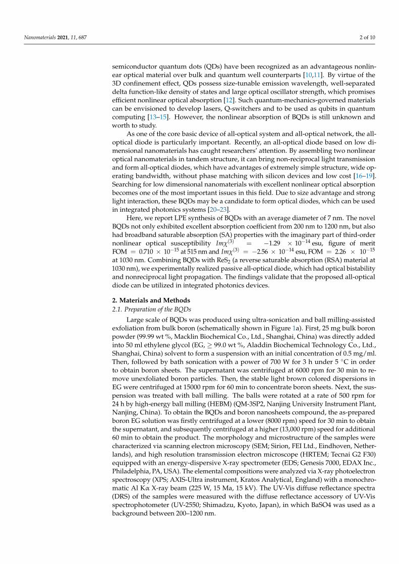
Figure 1. (a) schematic diagram of sonochemical and ball milling synthesis of boron quantum dots(BQDs). (b) TEM images of boron sheets obtained by sonochemical exfoliation in ethylene glycol(EG), the insets of (b) show the high resolution transmission electron microscope (HRTEM) of boronsheets. (c) TEM image of boron nanosheets (BNSs) and BQDs compound. (d) TEM images of BQDs,the inset of (d) shows the HRTEM of BQDs. (e) Atomic Force Microscope (AFM) characterization ofthe BQDs. (f) statistical data for BQDs showing the average thickness. (g) XPS spectrum (survey)for BQDs. (h) electron energy loss spectroscopy (EELS) studies of BQDs, the inset of (h) shows thecorresponding atomic ratios of BQDs.
2.2. Characterization of BQDs
In the planetary ball mill, the collapse of cavitation bubbles would lead to high-speedliquid micro-jets, inducing the layer gaps in bulk boron as well as the intercalation and exfo-liation by the super-critical fluids. As shown in Figure 1a, balls with the diameter of 10 mm,5 mm and 2 mm would reduce the size of boron nanosheets and ultimately grind boronnanosheets (BNSs) into BQDs. In order to measure the morphology and crystallinity ofBQDs, the transmission electron microscopy (TEM) was conducted. As shown in Figure 1b,many randomly oriented few-layer boron sheets and a small number of atomically thinboron sheets were found in the EG-exfoliated bulk boron sample. The HRTEM observation(insets of Figure 1b) further demonstrated the crystalline nature of the few-layer boronsheets, which shows a clear fringe with a d-spacing of 0.50 nm, corresponding to the(104) plane of β-rhombohedral boron structure. After HEBM, it obtained BNSs and BQDscompound in Figure 1c [24,25]. To purify BNSs and BQDs compound, we modulated theappropriate centrifugation speed and time. As shown in Figure 1d, the size of BQDs isrelatively uniform, which is consistent with the AFM results in Figure 1e. The HRTEMobservation (insets of Figure 1d) further demonstrated the diameter of BQDs is around7 nm, which is match with the statistical data of BQDs in Figure 1f. Figure 1g is bindingenergy spectrum characterized by XPS (VG Multilab 2000). It exhibits a high peak forbinding energies ranging from 185 Ev to 195 Ev, which is believed to be the high-resolutionB 1s spectra of BQDs. Furthermore, the spectra can be fitted by three Gaussian profiles thatare centered at 187.6 Ev, 189.3 Ev and 191.3 Ev, respectively. This finding indicates that there
Nanomaterials 2021, 11, 687 4 of 10
are three components of bonding structures of boron. The main component at 187.6 Evcorresponds to a B-B bond, which is consistent with the reported value for bulk boron [25].The other two components are mainly due to the oxidation of boron. The peak at 191.3 Evcan be assigned to the B-O bond in boron-rich oxide. The peak at 189.3 Ev may arise fromthe formation of a B-C bond due to exposure to air [25]. Results of electron energy lossspectroscopy (EELS) for BQDs are shown in Figure 1h. It exhibits a characteristic boronK-shell ionization edge at ∼188 Ev [24]. The inset of Figure 1h shows the correspondingatomic ratios of B, C and O in BQDs are 60.29 at.%, 36.44 at.% and 3.28 at.%, respectively.Small amount of O may arise from the surface contamination occurring during exposure toair atmosphere and the large amount of C may be due to the participation of carbon netsubstrate in the XPS measurements.
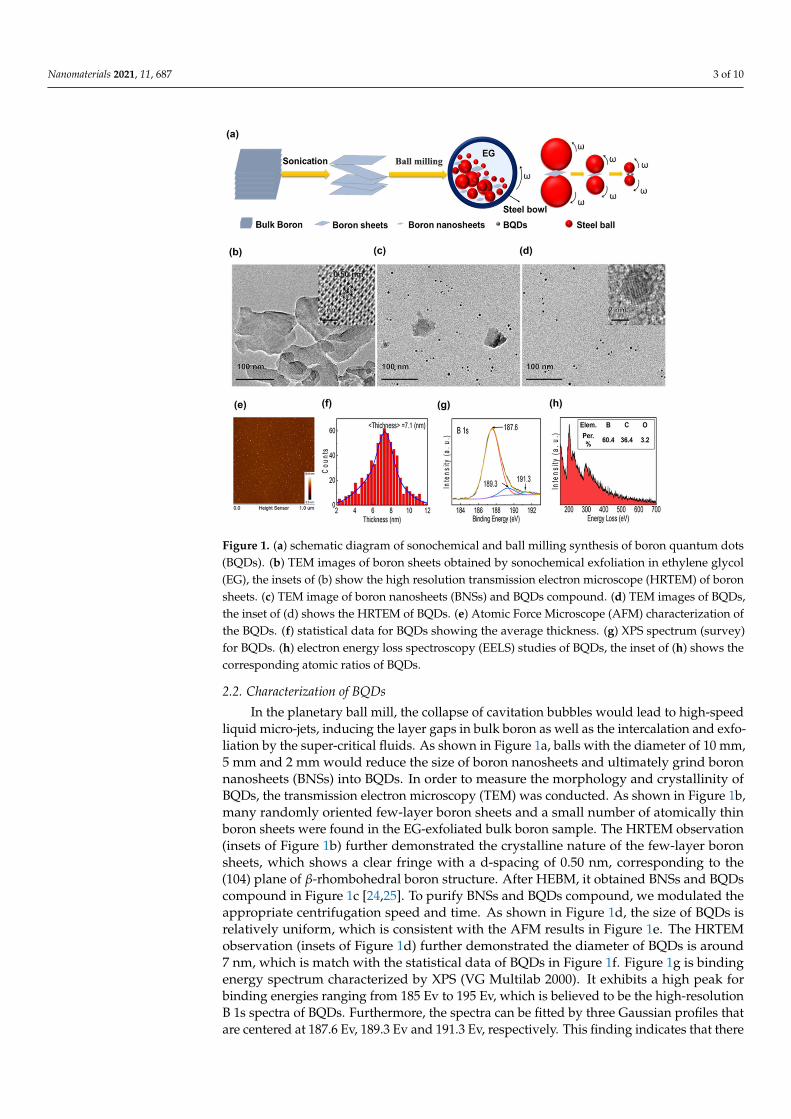
The linear absorption curves are shown in Figure 2a. Compared with EG-exfoliatedBNSs dispersions, BQDs dispersions exhibit stronger and broader optical absorption from200 nm to 1200 nm. We calculated and deduced the band gap of BQDs was ~0.6 Ev with thetauc model in Figure 2b. Compared to the Hao’s work [26], our BQDs own smaller bandgapand correspondingly cannot observe photoluminescence (PL) signals at the visible band.This may be due to the high pressure and squeezing during ball milling process, defects willinevitably be introduced into the samples, which can be seen in some HRTEM image asshown in Figure 2c. On the surface of the BQDs, we can observe some folds and bulges.The effect may affect the bandgap and absorption of the BQDs. However, it owns higherand broader linear optical absorptions. The excellent optical absorption indicates stronglight matter interaction in BQDs, which may lead excellent nonlinear optical property [27].
Figure 2. (a) UV-Vis-NIR absorption spectra of the BQDs and BNSs. (b) the corresponding opticalband gap of BQDs. (c) the HRTEM image of BQDs with defects on surface.
3. Results and Discussion3.1. The Nonlinear Absorption of the BQDs
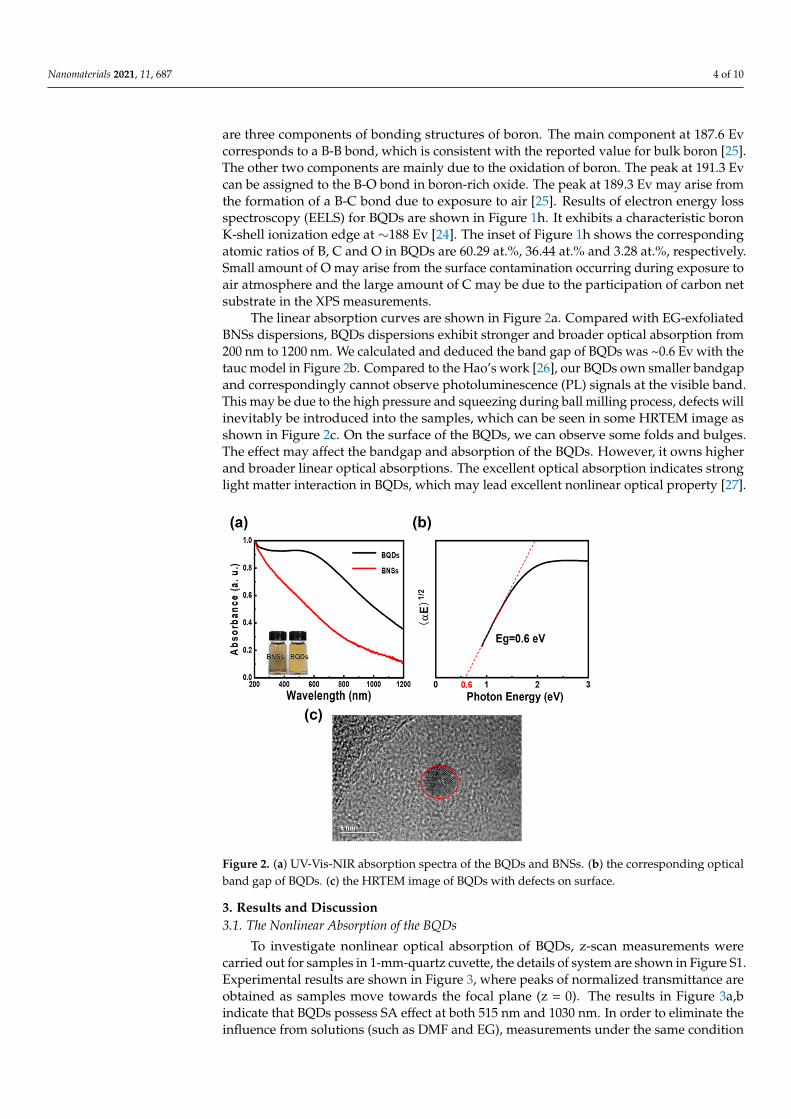
To investigate nonlinear optical absorption of BQDs, z-scan measurements werecarried out for samples in 1-mm-quartz cuvette, the details of system are shown in Figure S1.Experimental results are shown in Figure 3, where peaks of normalized transmittance areobtained as samples move towards the focal plane (z = 0). The results in Figure 3a,bindicate that BQDs possess SA effect at both 515 nm and 1030 nm. In order to eliminate theinfluence from solutions (such as DMF and EG), measurements under the same condition
Nanomaterials 2021, 11, 687 5 of 10
were done to confirm that the solutions do not exhibit SA effect. As a result, the SA effectcan be merely attributed to BQDs. Furthermore, thin films of BQDs were spin-coated onto0.5-mm-quartz substrates for z-scan measurements. The results were obtained at excitationwavelengths of 515 nm and 1030 nm, confirming the SA effect of BQDs as well. With theincrease of incident power, the amplitude of SA curve increases gradually, indicating thatthe BQDs do not produce photo-bleaching. Similarly, when the incident power decreasesgradually, the amplitude also decreases and can be repeated, indicating that the BQDs didnot produce photo-degradation.
Figure 3. (a,b) the open aperture z-scan measurements of BQDs under different intensities at 515 nmand 1030 nm, respectively. (c) the normalized transmittance and input intensity of BQDs at 515 nmand 1030 nm. (d) the open aperture z-scan measurements of BQDs and graphene nanosheets underthe excitation of 2 µJ/pulse at 1030 nm.
To evaluate the suitability and nonlinearity of prepared BQDs as SA for ultrafastphotonic devices, the most common SA model was used to fit the relationship betweenT(z) and input peak intensity [28,29].
T(z) = 1 − As(1 + IIsat)− Ans (1)
where As, I, Isat and Ans are the modulation depth, incident light intensity, saturableintensity and non-saturable loss, respectively. αNL ∼= −α0/Isat is fitted to be ~10−11
cm/W at 515 nm and 1030 nm, where negative values correspond to the SA process.However, the value of αNL is affected by the concentration. To further characterize opticalnonlinearities of BQDs, the imaginary part of the third-order nonlinear optical suscep-tibility [30] is Imχ(3) =
[10−7cλn2/
(96π2)] αNL, where c is the speed of light, λ is the
excitation wavelength and n is the refractive index. Values of Imχ(3) are −1.29 × 10⁻¹⁴ esuat 515 nm and −2.56 × 10⁻¹⁴ esu at 1030 nm. The figure of merit (FOM = Imχ(3)/α0) ofBQDs for the third-order optical nonlinearity is 0.710 × 10⁻¹⁵ at 515 nm and 2.26 × 10⁻¹⁵
at 1030 nm which are comparable to graphene in Figure 3d, biological tellurium PmPv
Nanomaterials 2021, 11, 687 6 of 10
(Bio-Te-PmPv) [30] and black phosphorus (BP) [17] listed in Table 1, and some other ma-terials [31–36]. The excellent nonlinear optical absorption performance of BQDs mayorigin from its strong light-matter interactions, which can be clearly seen from the linearabsorption spectrum on Figure 2a. Compared with nanosheets, the BQDs own larger light-matter interaction area. Otherwise, the quantum confinement effect will further enhanceinteraction between BQDs and light [37].
Table 1. Nonlinear optical coefficients of BQDs and other nanomaterials.
Laser Sample T (%) α0 (cm−1) Isat (GW/cm2) Imχ(3) (×10−14esu) FOM (×10−15) Ref.
515 nm, 340 fs Bio-Te-PmPV 54.0 6.17 201 ± 35 −(1.07 ± 0.11) 1.74 ± 0.18 [30]
515 nm, 340 fs BP dispersion 86.2 1.48 N/A −(0.49 ± 0.05) 3.30 ± 0.35 [17]
515 nm, 216 fs BQDs 17.7 17.30 575 ± 143 −(1.29 ± 0.38) 0.71 ± 0.19 This work
1030 nm, 340 fs Bio-Te-PmPV 52.4 6.47 145 ± 23 −(2.76 ± 0.58) 4.27 ± 0.91 [30]
1030 nm, 340 fs BP dispersion 80.3 2.19 N/A −(0.53 ± 0.12) 2.40 ± 0.49 [17]
1030 nm, 216 fs Graphene-NSs 75.5 2.81 49 ± 14 −(0.80 ± 0.11) 2.84 ± 0.41 This work
1030 nm, 216 fs BQDs 32.3 11.30 225 ± 64 −(2.56 ± 0.79) 2.26 ± 0.70 This work
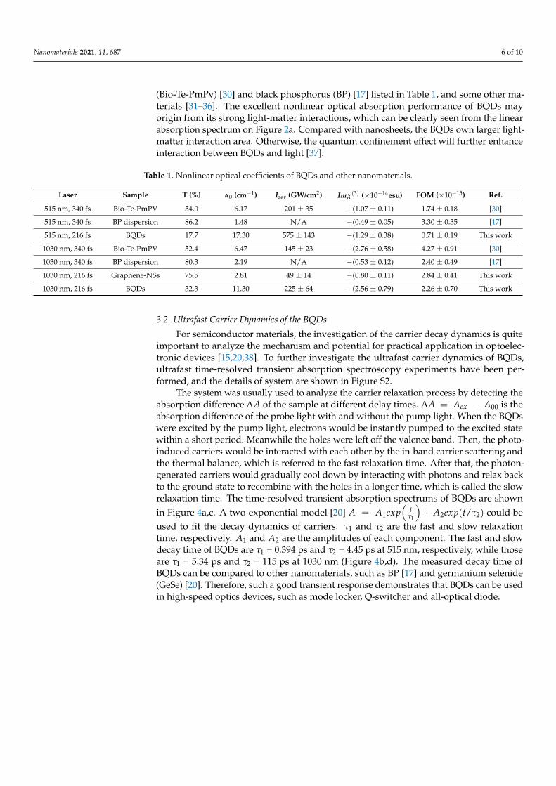
3.2. Ultrafast Carrier Dynamics of the BQDs
For semiconductor materials, the investigation of the carrier decay dynamics is quiteimportant to analyze the mechanism and potential for practical application in optoelec-tronic devices [15,20,38]. To further investigate the ultrafast carrier dynamics of BQDs,ultrafast time-resolved transient absorption spectroscopy experiments have been per-formed, and the details of system are shown in Figure S2.
The system was usually used to analyze the carrier relaxation process by detecting theabsorption difference ∆A of the sample at different delay times. ∆A = Aex − A00 is theabsorption difference of the probe light with and without the pump light. When the BQDswere excited by the pump light, electrons would be instantly pumped to the excited statewithin a short period. Meanwhile the holes were left off the valence band. Then, the photo-induced carriers would be interacted with each other by the in-band carrier scattering andthe thermal balance, which is referred to the fast relaxation time. After that, the photon-generated carriers would gradually cool down by interacting with photons and relax backto the ground state to recombine with the holes in a longer time, which is called the slowrelaxation time. The time-resolved transient absorption spectrums of BQDs are shownin Figure 4a,c. A two-exponential model [20] A = A1exp
(t
τ1
)+ A2exp(t/τ2) could be
used to fit the decay dynamics of carriers. τ1 and τ2 are the fast and slow relaxationtime, respectively. A1 and A2 are the amplitudes of each component. The fast and slowdecay time of BQDs are τ1 = 0.394 ps and τ2 = 4.45 ps at 515 nm, respectively, while thoseare τ1 = 5.34 ps and τ2 = 115 ps at 1030 nm (Figure 4b,d). The measured decay time ofBQDs can be compared to other nanomaterials, such as BP [17] and germanium selenide(GeSe) [20]. Therefore, such a good transient response demonstrates that BQDs can be usedin high-speed optics devices, such as mode locker, Q-switcher and all-optical diode.
Nanomaterials 2021, 11, 687 7 of 10
Figure 4. (a,c) the temporally and spectrally resolved transient absorption signal with probe lightfrom 500 nm to 650 nm and from 925 nm to 1050 nm, respectively. (b,d) the dynamic curves of BQDsfor various at 515 nm and 1030 nm, respectively.
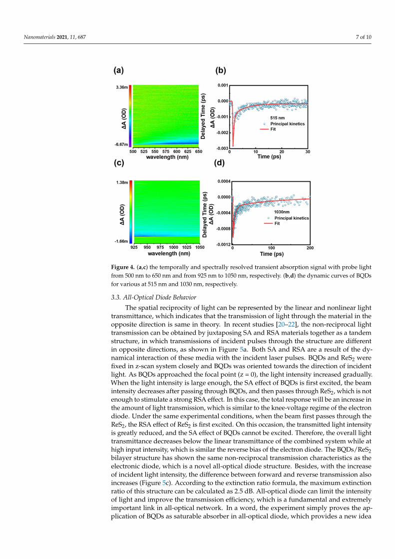
3.3. All-Optical Diode Behavior
The spatial reciprocity of light can be represented by the linear and nonlinear lighttransmittance, which indicates that the transmission of light through the material in theopposite direction is same in theory. In recent studies [20–22], the non-reciprocal lighttransmission can be obtained by juxtaposing SA and RSA materials together as a tandemstructure, in which transmissions of incident pulses through the structure are differentin opposite directions, as shown in Figure 5a. Both SA and RSA are a result of the dy-namical interaction of these media with the incident laser pulses. BQDs and ReS2 werefixed in z-scan system closely and BQDs was oriented towards the direction of incidentlight. As BQDs approached the focal point (z = 0), the light intensity increased gradually.When the light intensity is large enough, the SA effect of BQDs is first excited, the beamintensity decreases after passing through BQDs, and then passes through ReS2, which is notenough to stimulate a strong RSA effect. In this case, the total response will be an increase inthe amount of light transmission, which is similar to the knee-voltage regime of the electrondiode. Under the same experimental conditions, when the beam first passes through theReS2, the RSA effect of ReS2 is first excited. On this occasion, the transmitted light intensityis greatly reduced, and the SA effect of BQDs cannot be excited. Therefore, the overall lighttransmittance decreases below the linear transmittance of the combined system while athigh input intensity, which is similar the reverse bias of the electron diode. The BQDs/ReS2bilayer structure has shown the same non-reciprocal transmission characteristics as theelectronic diode, which is a novel all-optical diode structure. Besides, with the increaseof incident light intensity, the difference between forward and reverse transmission alsoincreases (Figure 5c). According to the extinction ratio formula, the maximum extinctionratio of this structure can be calculated as 2.5 dB. All-optical diode can limit the intensityof light and improve the transmission efficiency, which is a fundamental and extremelyimportant link in all-optical network. In a word, the experiment simply proves the ap-plication of BQDs as saturable absorber in all-optical diode, which provides a new idea
Nanomaterials 2021, 11, 687 8 of 10
for further exploring the optical properties and practical applications of low dimensionalboron materials.
Figure 5. (a) action of an all-optical diode based on asymmetric nonlinear absorption (NLA) byemploying a BQDs (saturable absorption (SA)) and ReS2 (reverse saturable absorption (RSA)) intandem. (b) the open aperture z-scan measurement of BQDs and ReS2 dispersions on 2.75 µJ/pulseat 1030 nm. (c) the light transmission in forward bias (BQDs/ReS2, red circle) and reverse bias(ReS2/BQDs, blue square).
As one of the core components of integrated photonics, the optical diode with a largeextinction ratio, broadband operation wavelength range, and low excitation thresholdhave been the motivation of researchers. All optical diode of tandem structure withlow dimensional boron materials provides many advantages, such as no phase-matchingconstraints, low cost and broadband operation wavelength range. They still face somechallenges such as the small extinction ratio and a high threshold, which encourage us toinvestigate in the near future.
4. Conclusions
In conclusion, we have developed sonochemical and ball milling synthesis of BQDsdispersions. It was found that BQDs exhibited completely different optical propertiesfrom bulk boron. The experiment proved that the BQDs had a SA effect at 515 nm and1030 nm, and had similar Imχ(3) and FOM as the graphene with excellent nonlinearoptical properties. Besides, the fast and slow relaxation times at different wavelengthsof 515 nm and 1030 nm were components with a lifetime of about 0.394 ps ~5.34 ps and4.45 ps ~115 ps, respectively. According to the results of transient absorption spectroscopy,BQDs not only possess ultrafast recovery times, but also exhibit SA effect. Using BQDs assaturable absorber to realize nonreciprocal all-optical diode opens a new way to explorethe application of LD boron in optics. The all-optical diode with low threshold and wideoperating bandwidth can be widely used in various fields such as photonic computing,all-optical networks, quantum communications and optical information processing.
Supplementary Materials: The following are available online at https://www.mdpi.com/2079-4991/11/3/687/s1, Figure S1: Schematic diagram of the Z-scan experimental setup, Figure S2: Schematicdiagram of the employed non-degenerate transient absorption experiment.
Nanomaterials 2021, 11, 687 9 of 10
Author Contributions: S.M., Q.C. and H.L. contributed equally to this work. Conceptualization, S.L.,C.P. and S.M.; Methodology, validation, Q.C.; Investigation resources, H.L.; Writing, S.M., Q.C. andH.L.; Data curation, S.M., Q.C. and H.L.; Revising, F.Z., S.L. and Y.G.; Project administration, C.P. andS.L.; Funding acquisition, S.L. and F.Z. All authors have read and agreed to the published version ofthe manuscript.
Funding: The authors are grateful for financial support from the Science and Technology InnovationCommission of Shenzhen (JCYJ20170302153323978, JCYJ20170410171958839); China Postdoctoral Sci-ence Foundation (2020M672763); Education Commission of Guangdong Province (2016KCXTD006);Instrumental Analysis Center of Shenzhen University.
Data Availability Statement: The data presented in this study are available on request from thecorresponding author.
Acknowledgments: The authors thank Instrumental Analysis Center of Shenzhen University forhelp in characterization of samples.
Conflicts of Interest: The authors declare no conflict of interest. The funders had no role in the designof the study; in the collection, analyses, or interpretation of data; in the writing of the manuscript, orin the decision to publish the results.
References1. Novoselov, K.S.; Geim, A.K.; Morozov, S.V.; Jiang, D.; Zhang, Y.; Dubonos, S.V.; Grigorieva, I.V.; Firsov, A.A. Electric Field Effect
in Atomically Thin Carbon Films. Science 2004, 306, 666. [CrossRef]2. Rezapour, M.R.; Myung, C.W.; Yun, J.; Ghassami, A.; Li, N.; Yu, S.U.; Hajibabaei, A.; Park, Y.; Kim, K.S. Graphene and
Graphene Analogs toward Optical, Electronic, Spintronic, Green-Chemical, Energy-Material, Sensing, and Medical Applications.ACS Appl. Mater. Interfaces 2017, 9, 24393. [CrossRef]
3. Xie, S.Y.; Wang, Y.L.; Li, X.B. Flat Boron: A New Cousin of Graphene. Adv. Mater. 2019, 31, 1900392. [CrossRef]4. Sun, X.; Liu, X.; Yin, J.; Yu, J.; Li, Y.; Hang, Y.; Zhou, X.; Yu, M.; Li, J.; Tai, G.; et al. Two-Dimensional Boron Crystals:
Structural Stability, Tunable Properties, Fabrications and Applications. Adv. Funct. Mater. 2017, 27, 1603300. [CrossRef]5. Zhang, Z.; Penev, E.S.; Yakobson, B.I. Two-dimensional boron: Structures, properties and applications. Chem. Soc. Rev. 2017,
46, 6746. [CrossRef] [PubMed]6. Zhou, X.F.; Mannix, A.J.; Kiraly, B.; Wood, J.D.; Alducin, D.; Myers, B.D.; Liu, X.L.; Fisher, B.L.; Santiago, U.; Guest, J.R.; et al.
Synthesis of borophenes: Anisotropic, two-dimensional boron polymorphs. Science 2015, 350, 6267.7. Xu, S.G.; Zhao, Y.J.; Liao, J.H.; Yang, X.B.; Xu, H. The nucleation and growth of borophene on the Ag (111) surface. Nano Res.
2016, 9, 2616. [CrossRef]8. Paton, K.R.; Varrla, E.; Backes, C.; Smith, R.J.; Khan, U.; O’Neill, A.; Boland, C.; Lotya, M.; Istrate, O.M.; King, P.; et al.
Scalable production of large quantities of defect-free few-layer graphene by shear exfoliation in liquids. Nat. Mater. 2014, 13, 624.[CrossRef]
9. Coleman, J.N.; Lotya, M.; O’Neill, A.; Bergin, S.D.; King, P.J.; Khan, U.; Young, K.; Gaucher, A.; De, S.; Smith, R.J.; et al.Two-Dimensional Nanosheets Produced by Liquid Exfoliation of Layered Materials. Science 2011, 331, 568. [CrossRef]
10. Chen, R.Z.; Zheng, X.; Jiang, T. Giant nonlinear absorption and excited carrier dynamics of black phosphorus few-layer nanosheetsin broadband spectra. Opt. Express 2017, 25, 7507. [CrossRef]
11. Xu, Y.H.; Wang, Z.T.; Guo, Z.N.; Huang, H.; Xiao, Q.; Zhang, H.; Yu, X.F. Solvothermal Synthesis and Ultrafast Photonics of BlackPhosphorus Quantum Dots. Adv. Optical Mater. 2016, 4, 1223. [CrossRef]
12. Zou, H.Y.; Liu, Z.X.; Wang, N.; Yang, T.; Peng, Z.W.; Wang, J.; Li, N.; Huang, C.Z. Photoluminescence of carbon quantum dots:Coarsely adjusted by quantum confinement effects and finely by surface trap states. Sci. China Chem. 2018, 61, 490.
13. Du, W.N.; Chen, J.; Shi, J.W.; Li, M.L.; Wang, Y.; Zhang, Q.; Liu, X.F. Perovskite quantum dot lasers. InfoMat 2020, 2, 170.14. Guo, Q.B.; Wu, K.; Shao, Z.P.; Basore, E.T.; Jiang, P.; Qiu, J.R. Boron Nanosheets for Efficient All-Optical Modulation and Logic
Operation. Adv. Optical Mater. 2019, 7, 1900322. [CrossRef]15. Shi, R.C.; Guo., J.; Wang, R.Y.; Wang, Z.; Zhang, F.; Wang, C.; Chen, H.L.; Ma, C.Y.; Wang, Z.H.; Ge, Y.Q.; et al. Graphdiyne-Polymer
Nanocomposite as a Broadband and Robust Saturable Absorber for Ultrafast Photonics. Laser Photonics Rev. 2020, 14, 1900367.16. Wu, L.; Dong, Y.; Zhao, J.; Ma, D.; Huang, W.; Zhang, Y.; Wang, Y.; Jiang, X.; Xiang, Y.; Li, J.; et al. Kerr Nonlinearity in 2D
Graphdiyne for Passive Photonic Diodes. Adv. Mater. 2019, 31, 1807981. [CrossRef] [PubMed]17. Dong, N.G.; Huang, J.W.; Zhang, S.F.; Sun, Z.Y.; Zhang, W.H.; Wang, J. Nonlinear Absorption Induced Transparency and Optical
Limiting of Black Phosphorus Nanosheets. ACS Photonics 2017, 4, 3063.18. Li, J.S.; Tang, Y.; Li, Z.T.; Rao, L.S.; Ding, X.R.; Yu, B.H. High efficiency solid-liquid hybrid-state quantum dot light-emitting
diodes. Photonics Res. 2018, 6, 1107. [CrossRef]19. Zhao, Q.; Yang, Z.J.; He, J. Coherent couplings between magnetic dipole transitions of quantum emitters and dielectric nanostruc-
tures. Photonics Res. 2019, 7, 1142. [CrossRef]
Nanomaterials 2021, 11, 687 10 of 10
20. Tang, J.; Zhang, F.; Zhou, F.; Tang, X.; Dai, X.; Lu, S. Broadband nonlinear optical response in GeSe nanoplates and its applicationsin all-optical diode. Nanophotonics 2020, 9, 2007–2015. [CrossRef]
21. Bi, L.; Hu, J.; Jiang, P.; Kim, H.S.; Kim, D.H.; Onbasli, M.C.; Dionne, G.F.; Ross, C.A. Magneto-Optical Thin Films for On-ChipMonolithic Integration of Non-Reciprocal Photonic Devices. Materials 2013, 6, 5094. [CrossRef] [PubMed]
22. Anand, B.; Podila, R.; Lingam, K.; Krishnan, S.R.; Siva Sankara Sai, S.; Philip, R.; Rao, A.M. Optical Diode Action from AxiallyAsymmetric Nonlinearity in an All-Carbon Solid-State Device. Nano. Lett. 2013, 13, 5771. [CrossRef]
23. Li, J.; Zhang, Z.; Du, L.; Miao, L.; Yi, J.; Huang, B.; Zou, Y.; Zhao, C.; Wen, S. Highly stable femtosecond pulse generation from aMXene Ti3C2Tx(T = F, O, or OH) mode-locked fiber laser. Photonics Res. 2019, 7, 260. [CrossRef]
24. Li, H.; Jing, L.; Liu, W.; Lin, J.; Tay, R.Y.; Tsang, S.H.; Teo, E.H.T. Scalable Production of Few-Layer Boron Sheets by Liquid-PhaseExfoliation and Their Superior Supercapacitive Performance. ACS Nano 2018, 12, 1262. [CrossRef] [PubMed]
25. Ranjan, P.; Sahu, T.K.; Bhushan, R.; Yamijala, S.S.; Late, D.J.; Kumar, P.; Vinu, A. Freestanding Borophene and Its Hybrids.Adv. Mater. 2019, 31, 1900353. [CrossRef]
26. Hao, J.Q.; Tai, G.A.; Zhou, J.X.; Wang, R.; Hou, C.; Guo, W.L. Crystalline Semiconductor Boron Quantum Dots. ACS Appl. Mater. Interfaces2020, 12, 17669. [CrossRef] [PubMed]
27. Yi, M.; Shen, Z.G. A review on mechanical exfoliation for scalable production of graphene. J. Mater. Chem. 2015, 3, 11700.[CrossRef]
28. Garmire, E. Resonant Optical Nonlinearities in Semiconductors. IEEE J. Sel. Top. Quantum Electron. 2000, 6, 1094. [CrossRef]29. Bao, Q.L.; Zhang, H.; Wang, Y.; Ni, Z.; Yan, Y.; Shen, Z.X.; Loh, K.P.; Tang, D.Y. Atomic-Layer Graphene as a Saturable Absorber
for Ultrafast Pulsed Laser. Adv. Funct. Mater. 2009, 19, 3077. [CrossRef]30. Wang, K.; Zhang, X.; Kislyakov, I.M.; Dong, N.; Zhang, S.; Wang, G.; Fan, J.; Zou, X.; Du, J.; Leng, Y.; et al. Bacterially synthesized
tellurium nanostructures for broadband ultrafast nonlinear optical applications. Nat. Commun. 2019, 10, 3985. [CrossRef]31. Kulyk, B.; Essaidi, Z.; Luc, J.; Sofiani, Z.; Boudebs, G.; Sahraoui, B.; Kapustianyk, V.; Turko, B. Second and third order nonlinear
optical properties of microrod ZnO films deposited on sapphire substrates by thermal oxidation of metallic zinc. J. Appl. Phys.2007, 102, 113113. [CrossRef]
32. Zawadzkaa, A.; Płóciennika, P.; Kouarib, Y.E.; Bougharrafc, H.; Sahraouid, B. Linear and nonlinear optical properties of ZnO thinfilms deposited by pulsed laser deposition. J. Lumin. 2016, 169, 483. [CrossRef]
33. Iliopoulos, K.; Czaplicki, R.; El Ouazzani, H.; Balandier, J.Y.; Chas, M.; Goeb, S.; Sallé, M.; Gindre, D.; Sahraoui, B. Physical originof the third order nonlinear optical response of orthogonal pyrrolo-tetrathiafulvalene derivatives. Appl. Phys. Lett. 2010,97, 101104. [CrossRef]
34. Kulyk, B.; Taboukhat, S.; Akdas-Kilig, H.; Fillaut, J.L.; Boughaleb, Y.; Sahraoui, B. Nonlinear refraction and absorption activity ofdimethylaminostyryl substituted BODIPY dyes. RSC Adv. 2016, 6, 88. [CrossRef]
35. Kulyk, B.; Guichaoua, D.; Ayadi, A.; El-Ghayoury, A.; Sahraoui, B. Functionalized azo-based iminopyridine rhenium complexesfor nonlinear optical performance. Dyes Pigment. 2017, 145, 256. [CrossRef]
36. Kulyk, B.; Waszkowska, K.; Busseau, A.; Villegas, C.; Hudhomme, P.; Dabos-Seignon, S.; Zawadzka, A.; Legoupy, S.; Sahraoui, B.Penta(zinc porphyrin)[60]fullerenes: Strong reverse saturable absorption for optical limiting applications. Appl. Surf. Sci. 2020,533, 147468. [CrossRef]
37. Valligatla, S.; Haldar, K.K.; Patra, A.; Desai, N.R. Nonlinear optical switching and optical limiting in colloidal CdSe quantum dotsinvestigated by nanosecond Z-scan measurement. Opt. Laser Techno. 2016, 84, 87. [CrossRef]
38. Zhang, F.; Chen, K.Q.; Wang, Y.Z.; Ge, Y.Q.; Wu, L.M.; Xu, S.X.; Bao, Q.L.; Zhang, H. Nonlinear optical absorption and ultrafastcarrier dynamics of copper antimony sulfide semiconductor nanocrystals. J. Mater. Chem. 2018, 6, 8977. [CrossRef]