Solid Tyre For Forklift | CS Easy SC20 | Solid Tyre Industry

SC20 Hardware Design
LTE Module Series
Rev: SC20_Hardware_Design_V1.2
Date: 2016-07-22
www.quectel.com

LTE Module Series SC20 Hardware Design
SC20_Hardware_Design Confidential / Released 1 / 95
Our aim is to provide customers with timely and comprehensive service. For any
assistance, please contact our company headquarters:
Quectel Wireless Solutions Co., Ltd.
Office 501, Building 13, No.99, Tianzhou Road, Shanghai, China, 200233
Tel: +86 21 5108 6236
Email: [email protected]
Or our local office. For more information, please visit:
http://www.quectel.com/support/salesupport.aspx
For technical support, or to report documentation errors, please visit:
http://www.quectel.com/support/techsupport.aspx
Or email to: [email protected]
GENERAL NOTES
QUECTEL OFFERS THE INFORMATION AS A SERVICE TO ITS CUSTOMERS. THE INFORMATION
PROVIDED IS BASED UPON CUSTOMERS’ REQUIREMENTS. QUECTEL MAKES EVERY EFFORT
TO ENSURE THE QUALITY OF THE INFORMATION IT MAKES AVAILABLE. QUECTEL DOES NOT
MAKE ANY WARRANTY AS TO THE INFORMATION CONTAINED HEREIN, AND DOES NOT ACCEPT
ANY LIABILITY FOR ANY INJURY, LOSS OR DAMAGE OF ANY KIND INCURRED BY USE OF OR
RELIANCE UPON THE INFORMATION. THE INFORMATION SUPPLIED HEREIN IS SUBJECT TO
CHANGE WITHOUT PRIOR NOTICE.
COPYRIGHT
THE INFORMATION CONTAINED HERE IS PROPRIETARY TECHNICAL INFORMATION OF
QUECTEL CO., LTD. TRANSMITTING, REPRODUCTION, DISSEMINATION AND EDITING OF THIS
DOCUMENT AS WELL AS UTILIZATION OF THE CONTENT ARE FORBIDDEN WITHOUT
PERMISSION. OFFENDERS WILL BE HELD LIABLE FOR PAYMENT OF DAMAGES. ALL RIGHTS
ARE RESERVED IN THE EVENT OF A PATENT GRANT OR REGISTRATION OF A UTILITY MODEL
OR DESIGN.
Copyright © Quectel Wireless Solutions Co., Ltd. 2016. All rights reserved.
Quectel
Confidential

LTE Module Series SC20 Hardware Design
SC20_Hardware_Design Confidential / Released 2 / 95
About the Document
History
Revision Date Author Description
1.0 2016-04-12 Tony GAO Initial
1.1 2016-05-04 Mark ZHANG 1. Updated RF Receiving Sensitivity
2. Updated Operation Temperature
1.2 2016-07-22 Sea BAI Added Chapters 2.4, 3.6~3.22, 4, 5 and 9
Quectel
Confidential

LTE Module Series SC20 Hardware Design
SC20_Hardware_Design Confidential / Released 3 / 95
Contents
About the Document ................................................................................................................................... 2
Contents ....................................................................................................................................................... 3
Table Index ................................................................................................................................................... 6
Figure Index ................................................................................................................................................. 8
1 Introduction ........................................................................................................................................ 10
1.1. Safety Information.................................................................................................................... 10
2 Product Concept ................................................................................................................................ 12
2.1. General Description ................................................................................................................. 12
2.2. Key Features ........................................................................................................................... 13
2.3. Functional Diagram ................................................................................................................. 15
2.4. Evaluation Board ..................................................................................................................... 16
3 Application Interfaces ....................................................................................................................... 17
3.1. General Description ................................................................................................................. 17
3.2. Pin Assignment ........................................................................................................................ 17
3.3. Pin Description ......................................................................................................................... 18
3.4. Power Supply ........................................................................................................................... 29
3.4.1. Power Supply Pins ......................................................................................................... 29
3.4.2. Decrease Voltage Drop .................................................................................................. 29
3.4.3. Reference Design for Power Supply .............................................................................. 30
3.5. Turn on and off Scenarios ....................................................................................................... 31
3.5.1. Turn on Module Using the PWRKEY ............................................................................. 31
3.5.2. Turn off Module .............................................................................................................. 33
3.6. VRTC Interface ........................................................................................................................ 34
3.7. Power Output ........................................................................................................................... 35
3.8. Battery Charge and Management ........................................................................................... 35
3.9. USB Interface .......................................................................................................................... 36
3.10. UART Interface ........................................................................................................................ 39
3.11. USIM Interface ......................................................................................................................... 40
3.12. SDIO Interface ......................................................................................................................... 42
3.13. GPIO Interface ......................................................................................................................... 44
3.14. I2C Interface ............................................................................................................................ 47
3.15. ADC Interface .......................................................................................................................... 48
3.16. Motor Drive Interface ............................................................................................................... 48
3.17. LCM Interface .......................................................................................................................... 49
3.18. Touch Panel Interface .............................................................................................................. 51
3.19. Camera Interface ..................................................................................................................... 52
3.19.1. Rear Camera Interface................................................................................................... 52
3.19.2. Front Camera Interface .................................................................................................. 54
3.19.3. Design Considerations ................................................................................................... 56
3.20. Sensor Interface ...................................................................................................................... 57
Quectel
Confidential

LTE Module Series SC20 Hardware Design
SC20_Hardware_Design Confidential / Released 4 / 95
3.21. Audio Interfaces ....................................................................................................................... 58
3.21.1. Reference Circuit Design for Microphone ...................................................................... 59
3.21.2. Reference Circuit Design for Receiver Interface ........................................................... 59
3.21.3. Reference Circuit Design for Headphone Interface ....................................................... 60
3.21.4. Reference Circuit Design for Loudspeaker Interface..................................................... 60
3.21.5. Audio Interface Design Considerations ......................................................................... 60
3.22. Emergency Download Interface .............................................................................................. 61
4 Wi-Fi and BT ....................................................................................................................................... 62
4.1. Wi-Fi Overview ........................................................................................................................ 62
4.1.1. Wi-Fi Performance ......................................................................................................... 62
4.2. BT Overview ............................................................................................................................ 63
4.2.1. BT Performance ............................................................................................................. 64
5 GNSS ................................................................................................................................................... 65
5.1. GNSS Performance ................................................................................................................. 65
5.2. GNSS RF Design Guidance .................................................................................................... 65
6 Antenna Interface ............................................................................................................................... 67
6.1. Main/Rx-diversity Antenna Interface ........................................................................................ 67
6.1.1. Pin Definition .................................................................................................................. 67
6.1.2. Operating Frequency ..................................................................................................... 67
6.1.3. Main and Rx-diversity Antenna Reference Design ........................................................ 68
6.2. Wi-Fi/BT Antenna Interface ..................................................................................................... 69
6.3. GNSS Antenna Interface ......................................................................................................... 69
6.3.1. Recommended Circuit for Passive Antenna .................................................................. 70
6.3.2. Recommended Circuit for Active Antenna ..................................................................... 70
6.4. Antenna Installation ................................................................................................................. 71
6.4.1. Antenna Requirement .................................................................................................... 71
6.4.2. Install the Antenna with RF Connector .......................................................................... 72
7 Electrical, Reliability and Radio Characteristics ............................................................................ 74
7.1. Absolute Maximum Ratings ..................................................................................................... 74
7.2. Power Supply Ratings ............................................................................................................. 74
7.3. Charging Performance Specifications ..................................................................................... 75
7.4. Operating Temperature ............................................................................................................ 75
7.5. Current Consumption .............................................................................................................. 76
7.6. RF Output Power ..................................................................................................................... 78
7.7. RF Receiving Sensitivity .......................................................................................................... 79
7.8. Electrostatic Discharge ............................................................................................................ 80
8 Mechanical Dimensions .................................................................................................................... 81
8.1. Mechanical Dimensions of the Module.................................................................................... 81
8.2. Recommended Footprint ......................................................................................................... 83
8.3. Top and Bottom View of the Module ........................................................................................ 84
9 Storage, Manufacturing and Packaging .......................................................................................... 85
Quectel
Confidential

LTE Module Series SC20 Hardware Design
SC20_Hardware_Design Confidential / Released 5 / 95
9.1. Storage..................................................................................................................................... 85
9.2. Manufacturing and Welding ..................................................................................................... 85
9.3. Packaging ................................................................................................................................ 86
10 Appendix A References ..................................................................................................................... 89
11 Appendix B GPRS Coding Schemes ............................................................................................... 93
12 Appendix C GPRS Multi-slot Classes .............................................................................................. 94
13 Appendix D EDGE Modulation and Coding Schemes ................................................................... 95
Quectel
Confidential

LTE Module Series SC20 Hardware Design
SC20_Hardware_Design Confidential / Released 6 / 95
Table Index
TABLE 1: SC20 FREQUENCY BANDS ..................................................................................................... 12
TABLE 2: SC20 KEY FEATURES .............................................................................................................. 13
TABLE 3: I/O PARAMETERS DEFINITION ............................................................................................... 19
TABLE 4: PIN DESCRIPTION ................................................................................................................... 19
TABLE 5: POWER DESCRIPTION ............................................................................................................ 35
TABLE 6: USB PIN DESCRIPTION ........................................................................................................... 37
TABLE 7: USB TRACE LENGTH INSIDE THE MODULE ......................................................................... 38
TABLE 8: PIN DESCRIPTION OF THE UART INTERFACE ..................................................................... 39
TABLE 9: PIN DEFINITION OF THE USIM INTERFACE .......................................................................... 40
TABLE 10: PIN DEFINITION OF THE SD CARD INTERFACE ................................................................ 43
TABLE 11: SDIO TRACE LENGTH INSIDE THE MODULE ...................................................................... 44
TABLE 12: PIN DEFINITION OF GPIO INTERFACE ................................................................................ 44
TABLE 13: PIN DEFINITION OF I2C INTERFACE ................................................................................... 47
TABLE 14: PIN DEFINITION OF THE ADC ............................................................................................... 48
TABLE 15: PIN DEFINITION OF MOTOR DRIVE INTERFACE ............................................................... 48
TABLE 16: PIN DEFINITION OF LCM INTERFACE ................................................................................. 49
TABLE 17: PIN DEFINITION OF TOUCH PANEL INTERFACE ................................................................ 51
TABLE 18: PIN DEFINITION OF REAR CAMERA INTERFACE............................................................... 53
TABLE 19: PIN DEFINITION OF FRONT CAMERA INTERFACE ............................................................ 54
TABLE 20: MIPI TRACE LENGTH INSIDE THE MODULE ....................................................................... 56
TABLE 21: PIN DEFINITION OF SENSOR INTERFACE .......................................................................... 57
TABLE 22: PIN DEFINITION OF AUDIO INTERFACE .............................................................................. 58
TABLE 23: WI-FI TRANSMITTING PERFORMANCE ............................................................................... 62
TABLE 24: WI-FI RECEIVING PERFORMANCE ...................................................................................... 63
TABLE 25: BT DATA RATE AND VERSION .............................................................................................. 64
TABLE 26: BT TRANSMITTING AND RECEIVING PERFORMANCE ...................................................... 64
TABLE 27: GNSS PERFORMANCE .......................................................................................................... 65
TABLE 28: PIN DEFINITION OF THE MAIN/RX-DIVERSITY ANTENNA................................................. 67
TABLE 29: SC20 MODULE OPERATING FREQUENCIES ...................................................................... 67
TABLE 30: PIN DEFINITION OF WI-FI/BT ANTENNA .............................................................................. 69
TABLE 31: WI-FI/BT FREQUENCY ........................................................................................................... 69
TABLE 32: PIN DEFINITION OF GNSS ANTENNA .................................................................................. 70
TABLE 33: GNSS FREQUENCY ............................................................................................................... 70
TABLE 34: ANTENNA REQUIREMENTS .................................................................................................. 71
TABLE 35: ABSOLUTE MAXIMUM RATINGS ........................................................................................... 74
TABLE 36: SC20 MODULE POWER SUPPLY RATINGS ......................................................................... 74
TABLE 37: CHARGING PERFORMANCE SPECIFICATIONS ................................................................. 75
TABLE 38: OPERATING TEMPERATURE ................................................................................................ 76
TABLE 39: SC20 CURRENT CONSUMPTION ......................................................................................... 76
TABLE 40: RF OUTPUT POWER .............................................................................................................. 78
TABLE 41: RF RECEIVING SENSITIVITY ................................................................................................ 79
Quectel
Confidential

LTE Module Series SC20 Hardware Design
SC20_Hardware_Design Confidential / Released 7 / 95
TABLE 42: ELECTROSTATIC DISCHARGE CHARACTERISTICS ( TEMPERATURE: 25℃, HUMIDITY:
45%) ......................................................................................................................................... 80
TABLE 43: REEL PACKAGING .................................................................................................................. 88
TABLE 44: RELATED DOCUMENTS ........................................................................................................ 89
TABLE 45: TERMS AND ABBREVIATIONS .............................................................................................. 89
TABLE 46: DESCRIPTION OF DIFFERENT CODING SCHEMES .......................................................... 93
TABLE 47: GPRS MULTI-SLOT CLASSES ............................................................................................... 94
TABLE 48: EDGE MODULATION AND CODING SCHEMES ................................................................... 95
Quectel
Confidential

LTE Module Series SC20 Hardware Design
SC20_Hardware_Design Confidential / Released 8 / 95
Figure Index
FIGURE 1: FUNCTIONAL DIAGRAM ........................................................................................................ 16
FIGURE 2: PIN ASSIGNMENT (TOP VIEW) ............................................................................................. 18
FIGURE 3: VOLTAGE DROP SAMPLE ..................................................................................................... 30
FIGURE 4: STAR STRUCTURE OF THE POWER SUPPLY .................................................................... 30
FIGURE 5: REFERENCE CIRCUIT OF POWER SUPPLY ....................................................................... 31
FIGURE 6: TURN ON THE MODULE USING DRIVING CIRCUIT ........................................................... 32
FIGURE 7: TURN ON THE MODULE USING KEYSTROKE .................................................................... 32
FIGURE 8: TIMING OF TURNING ON MODULE...................................................................................... 33
FIGURE 9: TIMING OF TURNING OFF MODULE .................................................................................... 33
FIGURE 10: RTC POWERED BY RECHARGEABLE BATTERY ............................................................. 34
FIGURE 11: RTC POWERED BY CAPACITOR ........................................................................................ 34
FIGURE 12: REFERENCE DESIGN FOR BATTERY CHARGING CIRCUIT ........................................... 36
FIGURE 13: USB INTERFACE REFERENCE DESIGN (DOES NOT SUPPORT OTG) .......................... 37
FIGURE 14: USB INTERFACE REFERENCE DESIGN (SUPPORT OTG) .............................................. 38
FIGURE 15: REFERENCE CIRCUIT WITH LEVEL TRANSLATOR CHIP (FOR UART1) ....................... 39
FIGURE 16: RS232 LEVEL MATCH CIRCUIT (FOR UART1) .................................................................. 40
FIGURE 17: REFERENCE CIRCUIT FOR USIM INTERFACE WITH AN 8-PIN USIM HOLDER............ 41
FIGURE 18: REFERENCE CIRCUIT FOR USIM INTERFACE WITH A 6-PIN USIM HOLDER .............. 42
FIGURE 19: REFERENCE CIRCUIT FOR SD CARD INTERFACE ......................................................... 43
FIGURE 20: REFERENCE CIRCUIT FOR MOTOR CONNECTION ........................................................ 49
FIGURE 21: REFERENCE CIRCUIT DESIGN FOR LCM INTERFACE ................................................... 50
FIGURE 22: REFERENCE DESIGN FOR BACKLIGHT DIRVING CIRCUIT ........................................... 51
FIGURE 23: REFERENCE CIRCUIT DESIGN FOR TP INTERFACE ...................................................... 52
FIGURE 24: REFERENCE CIRCUIT DESIGN FOR REAR CAMERA INTERFACE ................................ 54
FIGURE 25: REFERENCE CIRCUIT DESIGN FOR FRONT CAMERA INTERFACE .............................. 55
FIGURE 26: REFERENCE CIRCUIT DESIGN FOR MICROPHONE INTERFACE ................................. 59
FIGURE 27: REFERENCE CIRCUIT DESIGN FOR RECEIVER INTERFACE ........................................ 59
FIGURE 28: REFERENCE CIRCUIT DESIGN FOR HEADPHONE INTERFACE ................................... 60
FIGURE 29: REFERENCE CIRCUIT DESIGN FOR LOUDSPEAKER INTERFACE ............................... 60
FIGURE 30: REFERENCE CIRCUIT DESIGN FOR EMERGENCY DOWNLOAD INTERFACE ............. 61
FIGURE 31: REFERENCE CIRCUIT DESIGN FOR MAIN AND RX-DIVERSITY ANTENNA .................. 68
FIGURE 32: REFERENCE CIRCUIT DESIGN FOR WI-FI/BT ANTERNNA ............................................. 69
FIGURE 33: REFERENCE CIRCUIT DESIGN FOR GNSS PASSIVE ANTENNA ................................... 70
FIGURE 34: REFERENCE CIRCUIT DESIGN FOR GNSS ACTIVE ANTENNA ..................................... 71
FIGURE 35: DIMENSIONS OF THE UF.L-R-SMT CONNECTOR (UNIT: MM) ........................................ 72
FIGURE 36: MECHANICAL PARAMETERS OF UF.L-LP CONNECTORS .............................................. 73
FIGURE 37: SPACE FACTOR OF MATED CONNECTORS (UNIT: MM) ................................................. 73
FIGURE 38: MODULE TOP AND SIDE DIMENSIONS ............................................................................. 81
FIGURE 39: MODULE BOTTOM DIMENSIONS (TOP VIEW).................................................................. 82
FIGURE 40: RECOMMENDED FOOTPRINT (TOP VIEW) ...................................................................... 83
FIGURE 41: TOP VIEW OF THE MODULE .............................................................................................. 84
Quectel
Confidential

LTE Module Series SC20 Hardware Design
SC20_Hardware_Design Confidential / Released 9 / 95
FIGURE 42: BOTTOM VIEW OF THE MODULE ...................................................................................... 84
FIGURE 43: REFLOW SOLDERING THERMAL PROFILE ...................................................................... 86
FIGURE 44: TAPE SPECIFICATION ......................................................................................................... 87
FIGURE 45: REEL DIMENSIONS ............................................................................................................. 87
Quectel
Confidential

LTE Module Series SC20 Hardware Design
SC20_Hardware_Design Confidential / Released 10 / 95
1 Introduction
This document defines the SC20 module and describes its air interface and hardware interface which are
connected with your application.
This document can help you quickly understand module interface specifications, electrical and
mechanical details as well as other related information of SC20 module. Associated with application notes
and user guide, you can use SC20 module to design and set up mobile applications easily.
1.1. Safety Information
The following safety precautions must be observed during all phases of operation, such as usage, service
or repair of any cellular terminal or mobile incorporating SC20 module. Manufacturers of the cellular
terminal should send the following safety information to users and operating personnel and to incorporate
these guidelines into all manuals supplied with the product. If not so, Quectel assumes no liability for the
customer’s failure to comply with these precautions.
Full attention must be given to driving at all times in order to reduce the risk of an
accident. Using a mobile while driving (even with a handsfree kit) causes
distraction and can lead to an accident. You must comply with laws and regulations
restricting the use of wireless devices while driving.
Switch off the cellular terminal or mobile before boarding an aircraft. Make sure it is
switched off. The operation of wireless appliances in an aircraft is forbidden, so as
to prevent interference with communication systems. Consult the airline staff about
the use of wireless devices on boarding the aircraft, if your device offers an
Airplane Mode which must be enabled prior to boarding an aircraft.
Switch off your wireless device when in hospitals or clinics or other health care facilities. These requests are desinged to prevent possible interference with sentitive medical equipment.
Quectel
Confidential

LTE Module Series SC20 Hardware Design
SC20_Hardware_Design Confidential / Released 11 / 95
Cellular terminals or mobiles operating over radio frequency signal and cellular
network cannot be guaranteed to connect in all conditions, for example no mobile
fee or with an invalid SIM card. While you are in this condition and need emergent
help, please remember using emergency call. In order to make or receive a call,
the cellular terminal or mobile must be switched on and in a service area with
adequate cellular signal strength.
Your cellular terminal or mobile contains a transmitter and receiver. When it is ON ,
it receives and transmits radio frequency energy. RF interference can occur if it is
used close to TV set, radio, computer or other electric equipment.
In locations with potencially explosive atmospheres, obey all posted signs to turn
off wireless devices such as your phone or other cellular terminals. Areas with
potencially exposive atmospheres include fuelling areas, below decks on boats,
fuel or chemical transfer or storage facilities, areas where the air contains
chemicals or particles such as grain, dust or metal powders, etc.
Quectel
Confidential

LTE Module Series SC20 Hardware Design
SC20_Hardware_Design Confidential / Released 12 / 95
2 Product Concept
2.1. General Description
SC20 is a series of 4G smart modules based on Qualcomm platform and Android operating system, and
provides industrial grade performance. It supports worldwide LTE-FDD/LTE-TDD/WCDMA/
TD-SCDMA/EVDO/CDMA/GSM coverage, and also supports short-range wireless communication via
Wi-Fi 802.11b/g/n and BT4.1 LE. Additionally, SC20 integrates GPS/GLONASS/BeiDou satellite
positioning systems. Due to multiple speech and audio codecs as well as the built-in high performance
AdrenoTM
304 graphics processing unit, it enables smooth play of 720P videos. The module also offers
multiple audio and video input/output interfaces as well as abundant GPIO interfaces.
The following table shows the supported network types and frequency bands of SC20.
Table 1: SC20 Frequency Bands
Type Frequency
LTE-FDD B1/B3/B8
LTE-TDD B38/B39/B40/B41
WCDMA B1/B8
TD-SCDMA B34/B39
EVDO/CDMA BC0
GSM 900/1800MHz
Wi-Fi 802.11b/g/n 2402-2482MHz
BT4.1 LE 2402-2480MHz
GNSS GPS/GLONASS/BeiDou
SC20 is an SMD type module, which can be embedded into applications through its 210-pin pads
including 146 LCC signal pads and 64 other pads. With a compact profile of 40.5mm × 40.5mm × 2.8mm,
SC20 can meet almost all requirements for M2M applications such as automotive, metering, tracking,
security, routers, wireless POS, mobile computing devices, PDA phone, tablet PC, etc.
Quectel
Confidential

LTE Module Series SC20 Hardware Design
SC20_Hardware_Design Confidential / Released 13 / 95
2.2. Key Features
The following table describes the detailed features of SC20 module.
Table 2: SC20 Key Features
Feature Details
Applications Processor ARM Cortex-A7 microprocessor cores (quad-core) up to 1.1 GHz
512KB L2 cache
Multimedia Processor QDSP6 v5 core up to 691.2 MHz
768KB L2 cache
Memory 8GB EMMC+8Gb LPDDR3
Operating System Android OS 5.1
Power Supply Supply voltage: 3.5V~4.2V
Typical supply voltage: 3.8V
Transmitting Power
Class 4 (33dBm±2dB) for EGSM900
Class 1 (30dBm±2dB) for DCS1800
Class E2 (27dBm±3dB) for EGSM900 8-PSK
Class E2 (26dBm±3dB) for DCS1800 8-PSK
Class 3 (24dBm+1/-3dB) for WCDMA bands
Class 3 (24dBm+3/-1dB) for CDMA BC0
Class 2 (24dBm+1/-3dB) for TD-SCDMA bands
Class 3 (23dBm±2dB) for LTE FDD bands
Class 3 (23dBm±2dB) for LTE TDD bands
LTE Features
Support 3GPP R9 CAT4 FDD and TDD
Support 1.4 to 20 MHz RF bandwidth
Support DL 2 x 2 MIMO
Max 150Mbps (DL), 50Mbps (UL)
WCDMA Features
Support 3GPP R9 DC-HSPA+
Support 16-QAM, 64-QAM and QPSK modulation
3GPP R6 HSUPA: Max 11Mbps (UL)
3GPP R9 DC-HSPA+: Max 42Mbps (DL)
TD-SCDMA Features Support 3GPP R8 1.28 TDD
Max 4.2Mbps (DL), 2.2Mbps (UL)
CDMA Features Max 3.1Mbps (DL), 1.8Mbps (UL)
GSM/GPRS/EDGE
Data Features
GPRS
Support GPRS multi-slot class 33
Coding scheme: CS-1, CS-2, CS-3 and CS-4
Maximum of four Rx time slots per frame
Quectel
Confidential

LTE Module Series SC20 Hardware Design
SC20_Hardware_Design Confidential / Released 14 / 95
EDGE
Support EDGE multi-slot class 33
Support GMSK and 8-PSK
WLAN Features 2.4G single frequency band, support 802.11b/g/n, up to 150Mbps
Support AP mode
Bluetooth Feature BT4.1 LE
GNSS Features GPS/GLONASS/BeiDou
SMS
Text and PDU mode
Point to point MO and MT
SMS cell broadcast
SMS storage: ME by default
AT Commands Compliant with 3GPP TS 27.007, 27.005 and Quectel enhanced AT
commands
LCM Interface
4 lanes MIPI_DSI, up to 1.5Gbps each
Support WVGA (2 lanes MIPI_DSI), up to 720p (4 lanes MIPI_DSI)
24bit color depth
Camera Interface
Use MIPI_CSI, up to 1.5Gbps per lane, support two cameras
2-lane MIPI_CSI for rear camera, up to 8MP
1-lane MIPI_CSI for front camera, up to 2MP
Audio Interface
Audio input
2 groups analog microphone input, integrate internal bias voltage
Audio output
Class AB stereo headphone output
Class AB earpiece differential output
Class D speaker differential amplifier output
USB Interface
Compliant with USB 2.0 specification; the data transfer rate can reach
up to 480Mbps
Used for AT command communication, data transmission, software
debugging and firmware upgrade
Support USB OTG (Need additional 5V power supply chip)
USB Driver: Support Windows XP, Windows Vista, Windows 7,
Windows 8, Windows CE5.0/6.0*, Linux 2.6/3.0, Android 2.3/4.0/4.2
USIM Interface 2 groups of USIM interface
Support USIM/SIM card: 1.8V, 3.0V
UART Interface
2 groups of UART interface
4-wire UART interface with RTS and CTS hardware flow control
2-wire UART interface for software debugging
Baud rate up to 4Mbps
SDIO Interface Support SD3.0; 4bit SDIO; SD Card
Support hot plug
I2C Interface 3 groups I2C, with data rate up to 3.4Mbps (High speed);
used for TP, camera, sensor peripherals, etc.
Quectel
Confidential

LTE Module Series SC20 Hardware Design
SC20_Hardware_Design Confidential / Released 15 / 95
ADC Interface
Support 3 ADC interfaces;
used for input voltage sense, battery temperature detection and
general purpose ADC
Real Time Clock Implemented
Antenna Interface MAIN antenna, DRX antenna, GNSS antenna and Wi-Fi/BT antenna
Physical Characteristics
Size: 40.5±0.15 × 40.5±0.15 × 2.8±0.2 mm
Interface: LCC
Weight: approx. 9.6g
Temperature Range Operating temperature range: -35°C~+75°C
1)
Extended temperature range : -40°C~+85°C 2)
Firmware Upgrade Over USB interface
RoHS All hardware components are fully compliant with EU RoHS directive
1. 1)
Within operation temperature range, the module is 3GPP compliant.
2. 2)
Within extended temperature range, the module remains the ability to establish and maintain a
voice, SMS, data transmission, emergency call, etc. There is no unrecoverable malfunction. There
are also no effects on radio spectrum and no harm to radio network. Only one or more parameters
like Pout might reduce in their value and exceed the specified tolerances. When the temperature
returns to the normal operating temperature levels, the module will meet 3GPP compliant again.
3. * means this feature is under development.
2.3. Functional Diagram
The following figure shows a block diagram of SC20 and illustrates the major functional parts.
Power management
Radio frequency
Baseband
LPDDR3+EMMC flash
Peripheral interface
--USB interface
--USIM interface
--UART interface
--SDIO interface
--I2C interface
--ADC interface
NOTES
Quectel
Confidential

LTE Module Series SC20 Hardware Design
SC20_Hardware_Design Confidential / Released 16 / 95
--LCD (MIPI) interface
--TP interface
--CAM (MIPI) interface
--AUDIO interface
Baseband
PMIC
TransceiverLPDDR3+
EMMC
Duplexs
PA
Switch SAW Switch
ANT_MAIN ANT_DRXANT_GNSS
USB_VBUS
VBAT_RF
APT
PWRKEY
ADCs
LDO Output USB USIMTP UART I2C
AUDIO
19.2M
XO
GPIOs
VBAT_BB
LCD
(MIPI)CAM(MIPI) SDIO
SAW
ANT_WIFI/BT
WCN
LNA
SAW
SAW
SAW
TRX_CLK
RESET_N
VRTC
Figure 1: Functional Diagram
2.4. Evaluation Board
In order to help you to develop applications with SC20, Quectel supplies an evaluation board
(SMART-EVB), RS-232 to USB cable, USB data cable, power adapter, earphone, antenna and other
peripherals to control or test the module. For details, please refer to document [2].
Quectel
Confidential

LTE Module Series SC20 Hardware Design
SC20_Hardware_Design Confidential / Released 17 / 95
3 Application Interfaces
3.1. General Description
SC20 is equipped with 146-pin 1.0mm pitch SMT pads plus 64-pin ground pads and reserved pads that
can be embedded into cellular application platform. The following chapters provide the detailed
description of pins/interfaces listed below.
Power supply
VRTC interface
LCM interface
TP interface
Camera interface
Audio interface
USB interface
USIM interface
UART interface
SDIO interface
I2C interface
ADC interface
3.2. Pin Assignment
The following figure shows the pin assignment of SC20 module.
Quectel
Confidential

LTE Module Series SC20 Hardware Design
SC20_Hardware_Design Confidential / Released 18 / 95
GN
D
USB USIM OTHERS
102
GN
D
GN
D
GNDSDC2 GPIO ANTUART AUDIO I2C CAMERA
MIP
I_C
SI1
_L
N0
P
MIP
I_C
SI1
_L
N0
N
MIP
I_C
SI1
_C
LK
P
MIP
I_C
SI1
_C
LK
N
MIP
I_C
SI0
_L
N1
P
MIP
I_C
SI0
_L
N1
N
MIP
I_C
SI0
_L
N0
P
MIP
I_C
SI0
_L
N0
N
MIP
I_C
SI0
_C
LK
P
MIP
I_C
SI0
_C
LK
N
MIP
I_D
SI_
LN
3P
MIP
I_D
SI_
LN
3N
MIP
I_D
SI_
LN
2P
MIP
I_D
SI_
LN
2N
MIP
I_D
SI_
LN
1P
MIP
I_D
SI_
LN
1N
MIP
I_D
SI_
LN
0P
MIP
I_D
SI_
LN
0N
MIP
I_D
SI_
CL
KP
MIP
I_D
SI_
CL
KN
LC
D_
TE
TP
LC
D_
RS
T
VBAT_BB
VBAT_BB
GND
MIC1P
MIC_GND
MIC2P
1
2
3
4
5
6
7
8
9
10
11
12
13
14
15
16
17
18
19
20
21
22
23
24
25
26
27
28
29
30
31
32
33
34
35
36
37
38
39
40
41
42
43
44
45
46
47
48
49
50
51
52
53
54
55
56
57
58
59
60
61
62
63
64
65
66
67
68
69
70
71
72
73
94
93
92
91
90
89
88
87
86
85
84
83
82
81
80
79
78
77
76
75
74
101
100
99
98
97
96
95
103
102
105
104
107
106
109
108
110
11
2
11
1
11
4
11
3
11
6
11
5
11
8
11
7
11
9
12
1
12
0
12
3
12
2
12
5
12
4
12
6
12
8
12
7
13
0
12
9
13
2
13
1
13
3
13
5
13
4
13
7
13
6
13
9
13
8
14
0
14
2
14
1
14
4
14
3
14
6
14
5
148
147
152
151
154
167
169
168
170
165
164
166
163
180
181 188
1891
58
15
6
15
7
15
5
16
0
16
1
15
9
16
2
18
4
18
6
18
5
17
5
17
7
17
6
17
8
17
3
17
2
17
4
17
1
19
3
19
22
08
20
9
20
1
20
2
20
0
206
203
GND
EARP
EARN
VB
AT
_R
F
VB
AT
_R
F
GN
D
US
B_
VB
US
US
B_
VB
US
GN
D
GN
D
HS
_D
ET
HP
H_
L
HP
H_
GN
D
HP
H_
R
GN
D
VB
AT
_T
HE
RM
VB
AT
_S
NS
GN
D
GN
D
AN
T_
DR
X
AD
C
CH
AR
GE
_S
EL
LD
O1
7_
2V
85
VR
TC
LD
O6
_1
V8
GP
IO_
17
GP
IO_
16
GN
D
AN
T_
GN
SS
GN
D
GP
IO_
8
GP
IO_
9
GP
IO_
10
GP
IO_
11
GP
IO_
95
PW
RK
EY
GP
IO_
99
GP
IO_
58
LD
O5
_1
V8
GPIO_96
GPIO_65
GPIO_36
GPIO_94
GPIO_98
GPIO_0
GPIO_110
GPIO_97
GPIO_68
GPIO_69
GPIO_89
GPIO_88
GPIO_92
GPIO_31
KEY_VOL_DOWN
KEY_VOL_UP
UART2_TXD
UART2_RXD
SENSOR_I2C_SDA
SENSOR_I2C_SCL
GPIO_32
GND
GND
ANT_MAIN
GND
GND
CAM_I2C_SDA
CAM_I2C_SCL
CAM1_PWD
CAM1_RST
CAM0_PWD
CAM0_RST
GND
GND
ANT_WIFI/BT
CAM1_MCLK
CAM0_MCLK
SPKP
SPKN
GND
USB_DM
USB_DP
GND
USB_ID
USIM2_DETECT
USIM2_RST
USIM2_CLK
USIM2_DATA
USIM2_VDD
USIM1_DETECT
USIM1_RST
USIM1_CLK
USIM1_DATA
USIM1_VDD
GND
VIB_DRV
PWM
TP_INT
TP_RST
SD_LDO12
GPIO_23
UART1_TXD
UART1_RXD
UART1_CTS
UART1_RTS
SD
_L
DO
11
SD
_C
LK
SD
_C
MD
SD
_D
AT
A0
SD
_D
AT
A1
SD
_D
AT
A2
SD
_D
AT
A3
SD
_D
ET
US
B_
BO
OT
TP
_I2
C_
SC
L
TP
_I2
C_
SD
A
LCMPOWER
RESERVED
179
182
195
196
197
198 187
190
205
204
20
71
91
19
42
10
149
150
153
19
91
83
Figure 2: Pin Assignment (Top View)
3.3. Pin Description
The following tables show the SC20’s pin definition.
Quectel
Confidential

LTE Module Series SC20 Hardware Design
SC20_Hardware_Design Confidential / Released 19 / 95
Table 3: I/O Parameters Definition
Type Description
IO Bidirectional input/output
DI Digital input
DO Digital output
PI Power input
PO Power output
AI Analog input
AO Analog output
OD Open drain
Table 4: Pin Description
Power Supply
Pin Name Pin No. I/O Description DC
Characteristics Comment
VBAT_BB 1,2 PI
Power supply
for module
baseband
part.
Vmax=4.2V
Vmin=3.5V
Vnorm=3.8V
It must be able to provide
sufficient current up to
3.0A.
It is suggested to use a
zener diode for surge
protection. VBAT_RF 145,146 PI
Power supply
for module RF
part.
Vmax=4.2V
Vmin=3.5V
Vnorm=3.8V
VRTC 126 PI/PO
Power supply
for internal
RTC circuit.
VOmax=3.2V
VI=2.0V~3.25V
IIN max=200uA
If unused, keep this pin
open.
LDO5_1V8 111 PO Output 1.8V Vnorm=1.8V
IOmax=20mA
Power supply for external
GPIO’s pull up circuits and
level conversion circuit.
LDO6_1V8 125 PO Output 1.8V Vnorm=1.8V
IOmax=100mA
Power supply for
peripherals. 2.2uF~4.7uF
capacitor is recommended
to be applied to the
LDO6_1V8 pin. If unused,
keep this pin open.
Quectel
Confidential
LTE Module Series SC20 Hardware Design
SC20_Hardware_Design Confidential / Released 20 / 95
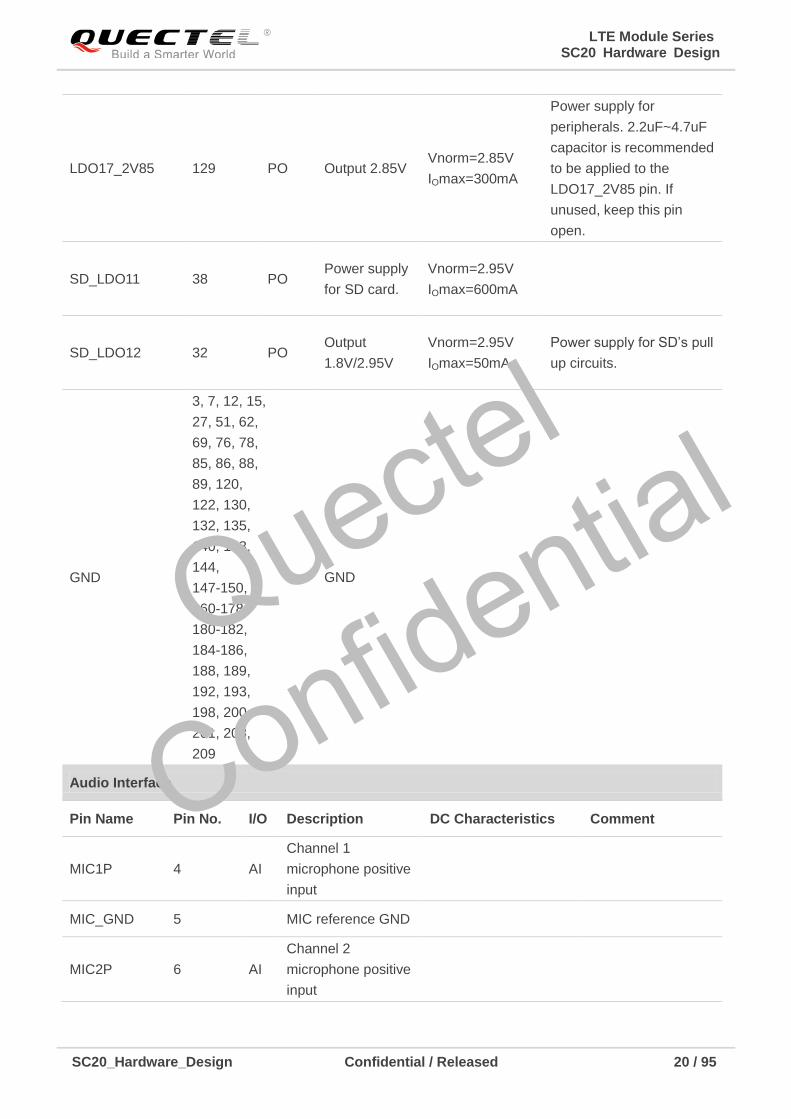
LDO17_2V85 129 PO Output 2.85V Vnorm=2.85V
IOmax=300mA
Power supply for
peripherals. 2.2uF~4.7uF
capacitor is recommended
to be applied to the
LDO17_2V85 pin. If
unused, keep this pin
open.
SD_LDO11 38 PO Power supply
for SD card.
Vnorm=2.95V
IOmax=600mA
SD_LDO12 32 PO Output
1.8V/2.95V
Vnorm=2.95V
IOmax=50mA
Power supply for SD’s pull
up circuits.
GND
3, 7, 12, 15,
27, 51, 62,
69, 76, 78,
85, 86, 88,
89, 120,
122, 130,
132, 135,
140, 143,
144,
147-150,
160-178,
180-182,
184-186,
188, 189,
192, 193,
198, 200,
201, 208,
209
GND
Audio Interface
Pin Name Pin No. I/O Description DC Characteristics Comment
MIC1P 4 AI
Channel 1
microphone positive
input
MIC_GND 5 MIC reference GND
MIC2P 6 AI
Channel 2
microphone positive
input
Quectel
Confidential

LTE Module Series SC20 Hardware Design
SC20_Hardware_Design Confidential / Released 21 / 95
EARP 8 AO Earpiece positive
output
EARN 9 AO Earpiece negative
output
SPKP 10 AO Speaker positive
output
SPKN 11 AO Speaker negative
output
HPH_R 136 AO Headphone right
channel output
HPH_GND 137 Headphone virtual
GND
HPH_L 138 AO Headphone left
channel output
HS_DET 139 AI Headset insertion
detection
High level by
default.
USB Interface
Pin Name Pin No. I/O Description DC
CHARACTERISTICS Comment
USB_VBUS 141,142 PI USB power supply
Vmax=6.3V
Vmin=4.35V
Vnorm=5.0V
Used for USB 5V
power input and
USB detection.
USB_DM 13 IO USB differential
data bus (minus) Compliant with USB
2.0 standard
specification.
Require differential
impedance of 90Ω. USB_DP 14 IO
USB differential
data bus (positive)
USB_ID 16 AI USB ID detection. High level by
default.
USIM Interface
Pin Name Pin
No. I/O Description DC Characteristics Comment
USIM2_DETECT 17 DI USIM2 card input
detection.
VILmax=0.63V
VIHmin=1.17V
Active Low.
External pull-up
resistor is
required. If
unused, keep
this pin open.
USIM2_RST 18 DO Reset signal of
USIM2 card
VOLmax=0.4V
VOHmin=0.8×USIM2_VDD
USIM2_CLK 19 DO Clock signal of
USIM2 card
VOLmax=0.4V
VOHmin=0.8×USIM2_VDD
Quectel
Confidential

LTE Module Series SC20 Hardware Design
SC20_Hardware_Design Confidential / Released 22 / 95
USIM2_DATA 20 IO Data signal of
USIM2 card
VILmax=0.2×USIM2_VDD
VIHmin=0.7×USIM2_VDD
VOLmax=0.4V
VOHmin=0.8×USIM2_VDD
USIM2_VDD 21 PO Power supply for
USIM2 card.
For 1.8V USIM:
Vmax=1.85V
Vmin=1.75V
For 2.95V USIM:
Vmax=2.95V
Vmin=2.8V
Either 1.8V or
2.95V USIM
card is
supported by
the module
automatically.
USIM1_DETECT 22 DI USIM1 card input
detection.
VILmax=0.63V
VIHmin=1.17V
Active low.
External pull-up
resistor is
required. If
unused, keep
this pin open.
USIM1_RST 23 DO Reset signal of
USIM1 card.
VOLmax=0.4V
VOHmin=0.8×USIM1_VDD
USIM1_CLK 24 DO Clock signal of
USIM1 card.
VOLmax=0.4V
VOHmin=0.8×USIM1_VDD
USIM1_DATA 25 IO Data signal of
USIM1 card.
VILmax=0.2×USIM1_VDD
VIHmin=0.7×USIM1_VDD
VOLmax=0.4V
VOHmin=0.8×USIM1_VDD
USIM1_VDD 26 PO Power supply for
USIM1 card.
For 1.8V USIM:
Vmax=1.85V
Vmin=1.75V
For 2.95V USIM:
Vmax=2.95V
Vmin=2.8V
Either 1.8V or
2.95V USIM
card is
supported by
the module
automatically
UART Interface
Pin Name Pin No. I/O Description DC Characteristics Comment
UART1_TXD 34 DO UART1 transmit
data.
VOLmax=0.45V
VOHmin=1.35V
1.8V power
domain.
If unused, keep
this pin open.
UART1_RXD 35 DI UART1 receive
data.
VILmax=0.63V
VIHmin=1.17V
1.8V power
domain.
If unused, keep
this pin open.
Quectel
Confidential

LTE Module Series SC20 Hardware Design
SC20_Hardware_Design Confidential / Released 23 / 95
UART1_CTS 36 DI UART1 clear to
send.
VILmax=0.63V
VIHmin=1.17V
1.8V power
domain.
If unused, keep
this pin open.
UART1_RTS 37 DO UART1 request to
send.
VOLmax=0.45V
VOHmin=1.35V
1.8V power
domain.
If unused, keep
this pin open.
UART2_RXD 93 DI UART2 receive
data.
VILmax=0.63V
VIHmin=1.17V
1.8V power
domain.
If unused, keep
this pin open.
UART2_TXD 94 DO UART2 transmit
data.
VOLmax=0.45V
VOHmin=1.35V
1.8V power
domain.
If unused, keep
this pin open.
SDIO/SD Interface
Pin Name Pin No. I/O Description DC Characteristics Comment
SD_CLK 39 DO SD Card
Clock
For 1.8V SD card:
VOLmax=0.45V
VOHmin=1.4V
For 2.95V SD card:
VOLmax=0.37V
VOHmin=2.2V
SD_CMD 40 IO SD Card CMD
For 1.8V SD card:
VILmax=0.58V
VIHmin=1.27V
VOLmax=0.45V
VOHmin=1.4V
For 2.95V SD card:
VILmax=0.73V
VIHmin=1.84V
VOLmax=0.37V
VOHmin=2.2V
SD_DATA0 41 IO SD Card
Data 0
For 1.8V SD card:
VILmax=0.58V
VIHmin=1.27V
Quectel
Confidential

LTE Module Series SC20 Hardware Design
SC20_Hardware_Design Confidential / Released 24 / 95
SD_DATA1 42 IO SD Card
Data 1
VOLmax=0.45V
VOHmin=1.4V
For 2.95V SD card:
VILmax=0.73V
VIHmin=1.84V
VOLmax=0.37V
VOHmin=2.2V
SD_DATA2 43 IO SD Card
Data 2
SD_DATA3 44 IO SD Card
Data 3
SD_DET 45 DI SD card input
detection.
VILmax=0.63V
VIHmin=1.17V Active low
Touch Panel (TP) Interface
Pin Name Pin No. I/O Description DC Characteristics Comment
TP_INT 30 DI Interrupt signal of
TP.
VILmax=0.63V
VIHmin=1.17V 1.8V power domain.
TP_RST 31 DO Reset signal of TP. VOLmax=0.45V
VOHmin=1.35V
1.8V power domain.
Active low.
TP_I2C_SCL 47 OD I2C clock signal of
TP. 1.8V power domain.
TP_I2C_SDA 48 OD I2C data signal of
TP. 1.8V power domain.
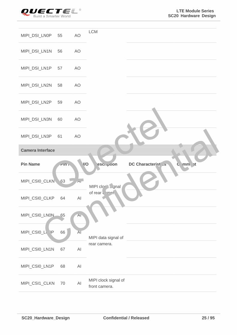
LCM Interface
Pin Name Pin
No. I/O Description DC Characteristics Comment
PWM 29 DO
Adjust the
backlight
brightness. PWM
control signal.
VOLmax=0.45V
VOHmax=VBAT_BB
LCD_RST 49 DO LCM reset signal VOLmax=0.45V
VOHmin=1.35V
1.8V power domain.
Active low.
LCD_TE 50 DI LCM tearing effect
signal.
VILmax=0.63V
VIHmin=1.17V 1.8V power domain.
MIPI_DSI_CLKN 52 AO Clock signal of
MIPI LCM
MIPI_DSI_CLKP 53 AO
MIPI_DSI_LN0N 54 AO Data signal of MIPI
Quectel
Confidential
LTE Module Series SC20 Hardware Design
SC20_Hardware_Design Confidential / Released 25 / 95
MIPI_DSI_LN0P 55 AO LCM
MIPI_DSI_LN1N 56 AO
MIPI_DSI_LN1P 57 AO
MIPI_DSI_LN2N 58 AO
MIPI_DSI_LN2P 59 AO
MIPI_DSI_LN3N 60 AO
MIPI_DSI_LN3P 61 AO
Camera Interface
Pin Name Pin No I/O Description DC Characteristics Comment
MIPI_CSI0_CLKN 63 AI
MIPI clock signal
of rear camera.
MIPI_CSI0_CLKP 64 AI
MIPI_CSI0_LN0N 65 AI
MIPI data signal of
rear camera.
MIPI_CSI0_LN0P 66 AI
MIPI_CSI0_LN1N 67 AI
MIPI_CSI0_LN1P 68 AI
MIPI_CSI1_CLKN 70 AI MIPI clock signal of
front camera.
Quectel
Confidential
LTE Module Series SC20 Hardware Design
SC20_Hardware_Design Confidential / Released 26 / 95
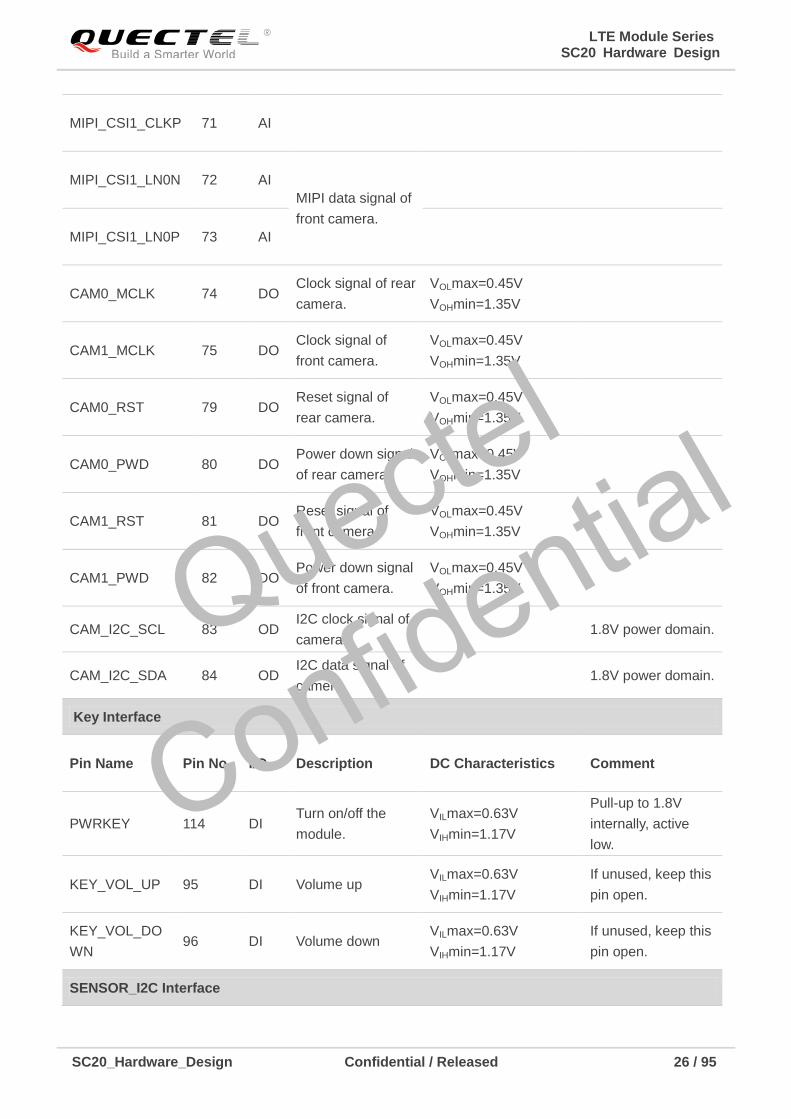
MIPI_CSI1_CLKP 71 AI
MIPI_CSI1_LN0N 72 AI
MIPI data signal of
front camera.
MIPI_CSI1_LN0P 73 AI
CAM0_MCLK 74 DO Clock signal of rear
camera.
VOLmax=0.45V
VOHmin=1.35V
CAM1_MCLK 75 DO Clock signal of
front camera.
VOLmax=0.45V
VOHmin=1.35V
CAM0_RST 79 DO Reset signal of
rear camera.
VOLmax=0.45V
VOHmin=1.35V
CAM0_PWD 80 DO Power down signal
of rear camera.
VOLmax=0.45V
VOHmin=1.35V
CAM1_RST 81 DO Reset signal of
front camera.
VOLmax=0.45V
VOHmin=1.35V
CAM1_PWD 82 DO Power down signal
of front camera.
VOLmax=0.45V
VOHmin=1.35V
CAM_I2C_SCL 83 OD I2C clock signal of
camera. 1.8V power domain.
CAM_I2C_SDA 84 OD I2C data signal of
camera. 1.8V power domain.
Key Interface
Pin Name Pin No. I/O Description DC Characteristics Comment
PWRKEY 114 DI Turn on/off the
module.
VILmax=0.63V
VIHmin=1.17V
Pull-up to 1.8V
internally, active
low.
KEY_VOL_UP 95 DI Volume up VILmax=0.63V
VIHmin=1.17V
If unused, keep this
pin open.
KEY_VOL_DO
WN 96 DI Volume down
VILmax=0.63V
VIHmin=1.17V
If unused, keep this
pin open.
SENSOR_I2C Interface
Quectel
Confidential

LTE Module Series SC20 Hardware Design
SC20_Hardware_Design Confidential / Released 27 / 95
Pin Name Pin No. I/O Description DC Characteristics Comment
SENSOR_I2C_
SCL 91 OD
I2C clock signal for
external sensor. 1.8V power domain.
SENSOR_I2C_
SDA 92 OD
I2C data signal for
external sensor. 1.8V power domain.
ADC Interface
Pin Name Pin No. I/O Description DC Characteristics Comment
ADC 128 AI General purpose
ADC.
Maximum voltage
not exceed 1.7V
VBAT_SNS 133 AI Input voltage
sense.
Maximum input
voltage is 4.5V.
VBAT_THERM 134 AI
Battery
temperature
detection.
RF Interface
Pin Name Pin No. I/O Description DC Characteristics Comment
ANT_MAIN 87 IO Main antenna
50Ω impedance
ANT_DRX 131 AI Diversity antenna
ANT_GNSS 121 AI GNSS antenna
ANT_WIFI/BT 77 IO Wi-Fi/BT antenna
GPIO Interface
Pin Name Pin No. I/O Description DC Characteristics Comment
GPIO_23 33 IO GPIO
GPIO_32 90 IO GPIO
GPIO_31 97 IO GPIO
GPIO_92 98 IO GPIO
GPIO_88 99 IO GPIO
GPIO_89 100 IO GPIO
Quectel
Confidential

LTE Module Series SC20 Hardware Design
SC20_Hardware_Design Confidential / Released 28 / 95
GPIO_69 101 IO GPIO
GPIO_68 102 IO GPIO
GPIO_97 103 IO GPIO
GPIO_110 104 IO GPIO
GPIO_0 105 IO GPIO
GPIO_98 106 IO GPIO
GPIO_94 107 IO GPIO
GPIO_36 108 IO GPIO
GPIO_65 109 IO GPIO
GPIO_96 110 IO GPIO
GPIO_58 112 IO GPIO
GPIO_99 113 IO GPIO
GPIO_95 115 IO GPIO
GPIO_11 116 IO GPIO
GPIO_10 117 IO GPIO
GPIO_9 118 IO GPIO
GPIO_8 119 IO GPIO
GPIO_16 123 IO GPIO
GPIO_17 124 IO GPIO
Other Interfaces
Pin Name Pin No. I/O Description DC Characteristics Comment
VIB_DRV 28 PO Motor drive.
Connected to the
negative terminal of
the motor.
RESET_N 179 DI Reset the module.
USB_BOOT 46 DI Force USB boot
control.
Set USB_BOOT pin
to high level will
force the module to
Quectel
Confidential
LTE Module Series SC20 Hardware Design
SC20_Hardware_Design Confidential / Released 29 / 95
enter into
emergency
download mode.
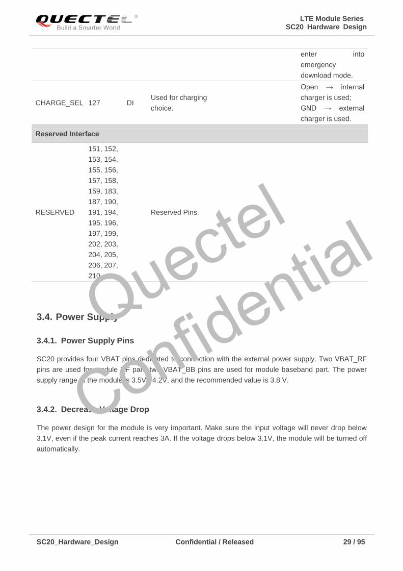
CHARGE_SEL 127 DI Used for charging
choice.
Open → internal
charger is used;
GND → external
charger is used.
Reserved Interface
RESERVED
151, 152,
153, 154,
155, 156,
157, 158,
159, 183,
187, 190,
191, 194,
195, 196,
197, 199,
202, 203,
204, 205,
206, 207,
210
Reserved Pins.
3.4. Power Supply
3.4.1. Power Supply Pins
SC20 provides four VBAT pins dedicated to connection with the external power supply. Two VBAT_RF
pins are used for module RF part; two VBAT_BB pins are used for module baseband part. The power
supply range of the module is 3.5V~ 4.2V, and the recommended value is 3.8 V.
3.4.2. Decrease Voltage Drop
The power design for the module is very important. Make sure the input voltage will never drop below
3.1V, even if the peak current reaches 3A. If the voltage drops below 3.1V, the module will be turned off
automatically.
Quectel
Confidential

LTE Module Series SC20 Hardware Design
SC20_Hardware_Design Confidential / Released 30 / 95
3.1V
Voltage3.8V
3A
Input current
Figure 3: Voltage Drop Sample
To decrease voltage drop, a bypass capacitor of about 100µF with low ESR should be used. Multi-layer
ceramic chip (MLCC) capacitor is recommended to be used due to its ultra-low ESR. Three ceramic
capacitors (100nF, 33pF, 10pF) are recommended to be applied to the VBAT pins. The main power
supply from an external application has to be a single voltage source and can be expanded to two sub
paths with star structure. The width of VBAT_BB trace should be no less than 1mm, and the width of
VBAT_RF trace should be no less than 2mm. In principle, the longer the VBAT trace is, the wider it will
be.
In addition, in order to get a stable power source, it is suggested to use a 0.5W zener diode and place it
as close to the VBAT pins as possible. The following figure shows the star structure of the power supply.
Module
VBAT_RF
VBAT_BB
VBAT
C1
100uF
C6
100nF
C7
33pF
C8
10pF
++
C2
100nF
C5
100uF
C3
33pF
C4
10pF
D1
Figure 4: Star Structure of the Power Supply
3.4.3. Reference Design for Power Supply
The power design for the module is very important, and the power supply should be capable of providing
sufficient current up to 3A at least. If the voltage drop between the input and output is not too high, it is
Quectel
Confidential

LTE Module Series SC20 Hardware Design
SC20_Hardware_Design Confidential / Released 31 / 95
suggested to use a LDO to supply power for the module. If there is a big voltage difference between the
input source and the desired output (VBAT), a buck converter is preferred to be used as the power
supply.
The following figure shows a reference design for +5V input power source. The designed output for the
power supply is about 3.8V and the maximum load current is 3A.
DC_IN
C1C2
MIC29302WU U1
IN OUT
EN
GN
D
AD
J
2 4
1 3 5
VBAT
100nF C3
470uF
C4
100nF
R2
100K
47K
R3
470uF
470R
51K R4
R1
1%
1%
MCU_POWER
_ON/OFF 47K
4.7KR5
R6
Figure 5: Reference Circuit of Power Supply
It is suggested that you should switch off the power supply for module in abnormal state, and then switch
on the power to restart the module.
3.5. Turn on and off Scenarios
3.5.1. Turn on Module Using the PWRKEY
The module can be turned on by driving PWRKEY pin to a low level for at least 1.6s. PWRKEY pin is
pulled to 1.8V internally. It is recommended to use an open drain/collector driver to control the PWRKEY.
A simple reference circuit is illustrated in the following figure.
NOTE Quectel
Confidential

LTE Module Series SC20 Hardware Design
SC20_Hardware_Design Confidential / Released 32 / 95
Turn on pulse
PWRKEY
4.7K
47K
≥ 1.6s
R1
R2
Q1
Figure 6: Turn on the Module Using Driving Circuit
The other way to control the PWRKEY is using a button directly. A TVS component is indispensable to be
placed nearby the button for ESD protection. A reference circuit is shown in the following figure.
PWRKEY
S1
Close to S1
TVS
Figure 7: Turn on the Module Using Keystroke
The turn on scenario is illustrated in the following figure.
Quectel
Confidential

LTE Module Series SC20 Hardware Design
SC20_Hardware_Design Confidential / Released 33 / 95
VBAT
PWRKEY
>1.6s
Others
1
LDO5_1V8
30s
LDO6_1V8
173ms
173.5ms
438msLDO17_2V85
Active
Figure 8: Timing of Turning on Module
Make sure that VBAT is stable before pulling down PWRKEY pin. The recommended time between them
is no less than 30ms. PWRKEY pin cannot be pulled down all the time.
3.5.2. Turn off Module
Set the PWRKEY pin low for at least 1s, and then choose to turn off the module when the prompt window
comes up.
The other way to turn off the module is to drive PWRKEY to a low level for at least 8s. The module will
execute forced shutdown. The forced power-down scenario is illustrated in the following figure.
VBAT
PWRKEY
Others
>8s
Power down
Figure 9: Timing of Turning off Module
NOTE
Quectel
Confidential

LTE Module Series SC20 Hardware Design
SC20_Hardware_Design Confidential / Released 34 / 95
3.6. VRTC Interface
The RTC (Real Time Clock) can be powered by an external power source through the pin VRTC when the
module is powered down and there is no power supply for the VBAT. It is also available to charge the
battery on the VRTC when module is turned on. You can choose rechargeable battery, capacitor or
non-rechargeable battery depending on different applications. The following are some reference circuit
designs when an external battery or capacitor is utilized for powering RTC.
If RTC is ineffective, it can be synchronized when the module starts data connection after power on.
Rechargeable
Backup Battery
Module
RTC
Core
VRTC
Figure 10: RTC Powered by Rechargeable Battery
Large
Capacitance
Capacitor
Module
RTC
Core
VRTC
C
Figure 11: RTC Powered by Capacitor
2.0~3.25V input voltage range and 3.0V typical value for VRTC. When VBAT is disconnected, the
average consumption is 5uA.
When powered by VBAT, the RTC error is 50ppm. When powered by VRTC, the RTC error is
200ppm.
If rechargeable battery is used, the ESR of the battery should be less than 2K, and it is
recommended to use the MS621FE FL11E of SEIKO.
If large capacitance capacitor is selected, it is recommended to use a 100uF capacitor with low
ESR. The capacitor is able to power the real-time clock for 45 seconds.
Quectel
Confidential

LTE Module Series SC20 Hardware Design
SC20_Hardware_Design Confidential / Released 35 / 95
3.7. Power Output
SC20 supports output of regulated voltages for peripheral circuits.
During application, it is recommended to use parallel capacitors (33pF and 10pF) in the circuit to
suppress high frequency noise.
Table 5: Power Description
Pin Name Voltage Range
(V)
Default Voltage
(V)
Driving Current
(mA) IDLE
LDO5_1V8 - 1.8 20 KEEP
LDO6_1V8 - 1.8 100 No output
LDO17_2V85 - 2.85 300 No output
SD_LDO12 - 2.95 50
SD_LDO11 1.75~3.337 2.95 600
USIM1_VDD 1.75~3.337 1.8/2.95 50
USIM2_VDD 1.75~3.337 1.8/2.95 50
3.8. Battery Charge and Management
SC20 module can recharge over-discharged batteries. The battery charger in SC20 module supports
trickle charging, constant current charging and constant voltage charging modes, which optimizes the
charging procedure for Li-ion batteries.
Trickle charging: There are two steps in this mode. When the battery voltage is below 2.8V, a 90mA
trickle charging current is applied to the battery. When the battery voltage is charged up and is
between 2.8V and 3.2V, the charging current can be set to 450mA maximally.
Constant current mode (CC mode): When the battery is increased to between 3.2V and 4.2V, the
system will switch to CC mode. The maximum charging current is 1.44A when adapter is used for
battery charging; and the maximum charging current is 450mA while USB charging.
Constant voltage mode (CV mode): When the battery voltage reaches the final value 4.2V, the
system will switch to CV mode and the charging current will decrease gradually. When the charging
current is reduced to about 100mA (maximum value; can be set according to application demands),
the charging is completed.
Quectel
Confidential

LTE Module Series SC20 Hardware Design
SC20_Hardware_Design Confidential / Released 36 / 95
SC20 module supports battery temperature detection in the condition that the battery integrates a
thermistor (47K 1%, B4050 NTC thermistor by default; SDNT1608X473F4050FTF of SUNLORD is
recommended) and the thermistor is connected to VBAT_THERM pin. The default temperature range is
from -3.0 to 48.5℃. If VBAT_THERM pin is not connected, there will be malfunctions such as battery
charging failure, battery level display error, etc.
A reference design for battery charging circuit is shown as below.
GND
VBAT_SNS
VBAT_THERM
VBAT
0R
100uF
NTC
VBAT
33pF1uFESD ESD
1
2
3
USB_VBUSAdapter or USB
ModuleBattery
GNDC1 C2 C3
R1
D1 D2
Figure 12: Reference Design for Battery Charging Circuit
Mobile devices such as mobile phones and handheld POS systems are powered by batteries. When
different batteries are utilized, the charging and discharging curve has to be modified correspondingly so
as to achieve the best effect.
If thermistor is not available in the battery, or adapter is utilized for powering module, then there is only
need for VBAT and GND connection. In this case, the system may mistakenly judge that the battery
temperature is abnormal, which will cause battery charging failure. In order to avoid this, VBAT_THERM
should be connected to GND via a 47KΩ resistor. If VBAT_THERM is unconnected, the system will
unable to detect the battery, making battery cannot be charged.
VBAT_SNS pin must be connected. Otherwise, the module will have abnormalities in voltage detection,
as well as associated power on/off and battery charging and discharging issues.
3.9. USB Interface
SC20 contains one integrated Universal Serial Bus (USB) transceiver which complies with the USB 2.0
specification and supports high speed (480 Mbps) and full speed (12 Mbps) modes. The USB interface is
used for AT command communication, data transmission, software debugging and firmware upgrade.
Quectel
Confidential

LTE Module Series SC20 Hardware Design
SC20_Hardware_Design Confidential / Released 37 / 95
The following table shows the pin definition of USB interface.
Table 6: USB Pin Description
Pin Name Pin No. I/O Description Comment
USB_VBUS 141,142 PI USB power supply 4.35~6.3V.
Typical 5.0V.
USB_DM 13 IO USB differential data bus (minus). Require differential
impedance of 90Ω.
USB_DP 14 IO USB differential data bus (positive). Require differential
impedance of 90Ω.
USB_ID 16 AI USB ID detection Default high level
USB_VBUS can be powered by USB power or adapter. It can also be used for detecting USB connection,
as well as for battery charging via the internal PMU. The input voltage of power supply ranges from 4.35
to 6.3V, and the typical value is 5V. SC20 module supports charging management for a single Li-ion
battery, but varied charging parameters should be set for batteries with varied models or capacities. The
module is available a built-in linear-charging circuit which supports maximally 1.44A charging current.
The following are two USB interface reference designs for customers to choose from.
USB_DP
USB_DM
USB_VUSB1
2
3
4
5
USB_DP
USB_DM
VUSB
USB_ID
GND
GN
D
GN
D
GN
D
GN
D6 7
89
100nFModule
C1 D1 D2 D3
ESD ESD ESD
Figure 13: USB Interface Reference Design (Does Not Support OTG)
Quectel
Confidential

LTE Module Series SC20 Hardware Design
SC20_Hardware_Design Confidential / Released 38 / 95
10uFEN
VIN
SW
NC
VOUT
VOUT4
5
1
7
8
6
2 93A
GN
D
PG
ND
PG
ND
10K
22uF/
10V
1.0uH
AW3605DNR
USB_DP
USB_DM
USB_VUSB
USB_ID
1
2
3
4
5
USB_DP
USB_DM
VUSB
USB_ID
GND
GN
D
GN
D
GN
D
GN
D6 7
89
100nF
Module
VBAT GPIO
VBAT
C1
C2
L1
U1
R1
C3 D1 D2 D3 D4
ESDESDESD ESD
D5
Figure 14: USB Interface Reference Design (Support OTG)
SC20 supports OTG protocol. If OTG function is needed, please refer to the above figure for the reference
design. AW3605DNR is a high efficiency DC-DC chip manufactured by AWINIC, and users can choose
according to their own demands.
In order to ensure USB performance, please comply with the following principles while designing USB
interface.
It is important to route the USB signal traces as differential pairs with total grounding. The impedance
of USB differential trace is 90Ω.
Pay attention to the influence of junction capacitance of ESD component on USB data lines. Typically,
the capacitance value should be less than 2pF.
Do not route signal traces under crystals, oscillators, magnetic devices and RF signal traces. It is
important to route the USB differential traces in inner-layer with ground shielding on not only upper
and lower layer but also right and left sides.
Keep the ESD components as close as possible to the USB connector.
Make sure the trace length difference between USB_DM and USB_DP is not exceeding 6.6mm.
Table 7: USB Trace Length inside the Module
PIN Signal Length (mm) Length Difference (DP-DM)
13 USB_DM 29.43
-0.07
14 USB_DP 29.36
Quectel
Confidential

LTE Module Series SC20 Hardware Design
SC20_Hardware_Design Confidential / Released 39 / 95
3.10. UART Interface
The module provides two UART interfaces: one 4-line UART interface (UART1) and one 2-line debug
UART interface (UART2). UART1 supports hardware flow control.
The following table shows the pin definition.
Table 8: Pin Description of the UART Interface
Pin Name Pin No I/O Description Comment
UART1_TXD 34 DO UART1 transmit data 1.8V power domain. If it is
unused, keep it open.
UART1_RXD 35 DI UART1 receive data 1.8V power domain. If it is
unused, keep it open.
UART1_CTS 36 DI UART1 clear to send 1.8V power domain. If it is
unused, keep it open.
UART1_RTS 37 DO UART1 request to send 1.8V power domain. If it is
unused, keep it open.
UART2_RXD 93 DI UART2 receive data 1.8V power domain. If it is
unused, keep it open.
UART2_TXD 94 DO UART2 transmit data 1.8V power domain. If it is
unused, keep it open.
UART1 provides 1.8V logic level. A level translator should be used if your application is equipped with a
3.3V UART interface. A level translator TXS0104PWR provided by Texas Instrument is recommended.
The following figure shows the reference design.
VCCA VCCB
OE
A1
A2
A3
A4
GND
B1
B2
B3
B4
LDO5_1V8
UART1_RTS
UART1_RXD
UART1_CTS
UART1_TXD
RTS_3.3V
RXD_3.3V
CTS_3.3V
TXD_3.3V
VDD_3.3V
TXS0104EPWR
C1100pF
C2
U1100pF
Figure 15: Reference Circuit with Level Translator Chip (for UART1)
Quectel
Confidential

LTE Module Series SC20 Hardware Design
SC20_Hardware_Design Confidential / Released 40 / 95
The following figure is an example of connection between SC20 and PC. A voltage level translator and a
RS-232 level translator chip must be added between the module and PC, as these two UART interfaces
do not support the RS-232 level, while support the 1.8V CMOS level only.
TXS0104EPWR
RTS_3.3V
RXD_3.3V
CTS_3.3V
TXD_3.3V
UART1_RTS
UART1_RXD
UART1_CTS
UART1_TXD
RTS_1.8V
RXD_1.8V
CTS_1.8V
TXD_1.8V
VCCA
Module
GND GND
1.8V
VCCB
3.3V
DIN1
ROUT3
ROUT2
ROUT1
DIN4
DIN3
DIN2
DIN5
R1OUTB
FORCEON
/FORCEOFF/INVALID
3.3V
DOUT1
DOUT2
DOUT3
DOUT4
DOUT5
RIN3
RIN2
RIN1
VCC GND
OE
SN65C3238 DB-9
RTS
TXD
CTS
RXD
GND
Figure 16: RS232 Level Match Circuit (for UART1)
UART2 is similar to UART1. Please refer to UART1 reference circuit designs for UART2 circuit design.
3.11. USIM Interface
The USIM card interface circuitry meets ETSI and IMT-2000 SIM interface requirements. SC20 provides 2
USIM interfaces. Dual SIM Card Dual Standby is supported, but it is disabled by default. Both 1.8V and
2.95V USIM cards are supported, and the USIM card interface is powered by the internal power supply of
SC20 module.
Table 9: Pin Definition of the USIM Interface
Pin Name Pin No I/O Description Comment
USIM2_DETECT 17 DI USIM2 card input detection
Active Low. External pull-up resistor
is required. If unused, keep this pin
open.
USIM2_RST 18 DO Reset signal of USIM2 card
NOTE
Quectel
Confidential
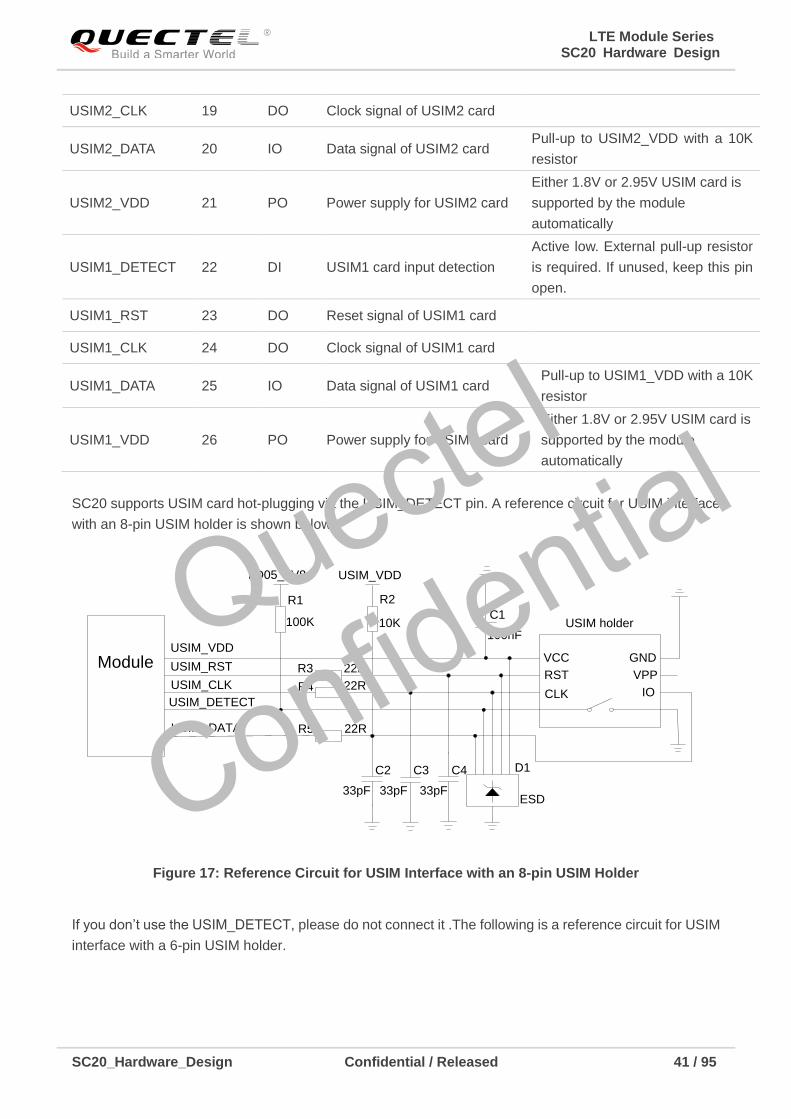
LTE Module Series SC20 Hardware Design
SC20_Hardware_Design Confidential / Released 41 / 95
USIM2_CLK 19 DO Clock signal of USIM2 card
USIM2_DATA 20 IO Data signal of USIM2 card Pull-up to USIM2_VDD with a 10K
resistor
USIM2_VDD 21 PO Power supply for USIM2 card
Either 1.8V or 2.95V USIM card is
supported by the module
automatically
USIM1_DETECT 22 DI USIM1 card input detection
Active low. External pull-up resistor
is required. If unused, keep this pin
open.
USIM1_RST 23 DO Reset signal of USIM1 card
USIM1_CLK 24 DO Clock signal of USIM1 card
USIM1_DATA 25 IO Data signal of USIM1 card Pull-up to USIM1_VDD with a 10K
resistor
USIM1_VDD 26 PO Power supply for USIM1 card
Either 1.8V or 2.95V USIM card is
supported by the module
automatically
SC20 supports USIM card hot-plugging via the USIM_DETECT pin. A reference circuit for USIM interface
with an 8-pin USIM holder is shown below.
USIM_VDD
USIM_RST
USIM_CLK
USIM_DATA
USIM_DETECT
22R
LD05_1V8
100K100nF
USIM holder
ESD33pF
VCC
RST
CLK IO
VPP
GND
USIM_VDD
10K
Module
R1 R2
C1
33pF33pF
C2 C3 C4 D1
22R
22R
R3
R4
R5
Figure 17: Reference Circuit for USIM Interface with an 8-pin USIM Holder
If you don’t use the USIM_DETECT, please do not connect it .The following is a reference circuit for USIM
interface with a 6-pin USIM holder.
Quectel
Confidential

LTE Module Series SC20 Hardware Design
SC20_Hardware_Design Confidential / Released 42 / 95
Module
USIM_VDD
USIM_RST
USIM_CLK
USIM_DATA 22R
22R
22R
100nFUSIM holder
ESD33pF
VCC
RST
CLK IO
VPP
GND
10K
USIM_VDD
33pF33pF
R1C1
D1
R2
R3
R4
C2 C3 C4
Figure 18: Reference Circuit for USIM Interface with a 6-pin USIM Holder
In order to ensure good performance and avoid damage of USIM cards, please follow the criteria below in
USIM circuit design:
Place USIM holder as close as possible to the module. Assure the trace length of USIM card signal is
less than 200mm.
Keep USIM card signal away from RF and VBAT alignment.
A 100nF filter capacitor shall be reserved for USIM_VDD, and its maximum capacitance should not
exceed 1uF. The capacitor should be placed near to USIM card.
To avoid cross-talk between USIM_DATA and USIM_CLK, keep them away from each other and
shield them with ground. USIM_RST also needs ground protection.
In order to offer good ESD protection, it is recommended to add TVS. The parasitic capacitance of
TVS should be not more than 50pF. The 22Ω resistors should be added in series between the
module and USIM card so as to suppress EMI. Please note that the USIM peripheral circuit should be
close to the USIM holder.
The 33pF capacitors should be added in parallel on USIM_DATA, USIM_CLK and USIM_RST signal
lines so as to filter RF interference, and they should be placed as close to the USIM holder as
possible.
3.12. SDIO Interface
SC20 module supports SD cards with 4-bit data interfaces or SDIO devices.
SD card interface pin definition and features are as follows.
Quectel
Confidential

LTE Module Series SC20 Hardware Design
SC20_Hardware_Design Confidential / Released 43 / 95
Table 10: Pin Definition of the SD Card Interface
Pin Name Pin No I/O Description Comment
SD_LDO11 38 PO Power supply for SD
card
SD_LDO12 32 PO SD card pull-up
power supply
Support 1.8V or 2.95V power
supply; the maximum drive
current is 50mA.
SD_CLK 39 DO High speed digital
clock
Control characteristic impedance
as 50Ω
SD_CMD 40 I/O SD card command
signal
SD_DATA0 41 I/O
High speed,
bidirectional digital
signals
SD_DATA1 42 I/O
SD_DATA2 43 I/O
SD_DATA3 44 I/O
SD_DET 45 DI SD card input
detection Active low
A reference circuit for SD card interface is shown as below.
SD_CMD
120K
NM_51K
SD_DATA3
SD_DATA2
LDO5_1V8
SD_CLK
SD_DATA0
SD_DET
SD_DATA1
P1-DAT2
P2-CD/DAT3
P3-CMD
P4-VDD
P5-CLK
P8-DAT1
GND
P6-VSS
P7-DAT0
DETECTIVE
GND
GND
GND
1
2
3
4
5
6
7
8
9
10
11
12
13
SD_LDO11
33R
33R
33R
33R
33R
33R
1K
33pF2.2uF
SD_LDO12
Module
R1 R2 R3 R4 R5 R6
NM_51K NM_10K NM_51K NM_51KR7
R8
R9
R10
R11
R12
R13
D1 D2 D3 D4 D5 D6 D7D8C1 C2
Figure 19: Reference Circuit for SD Card Interface
SD_LDO11 is a peripheral driver power supply for SD card. The maximum drive current is approx. 600mA.
Because of the high drive current, it is recommended that the trace width is 0.5mm. In order to ensure the
stability of drive power, a 2.2uF and a 33pF capacitor should be added in parallel near the SD socket.
Quectel
Confidential

LTE Module Series SC20 Hardware Design
SC20_Hardware_Design Confidential / Released 44 / 95
CMD, CLK, DATA0, DATA1, DATA2 and DATA3 are all high speed signal lines. In PCB design, please
control the characteristic impedance as 50Ω, and don’t cross with other traces. It is recommended to
route the trace on the inner layer of PCB, and to keep the same trace length for CMD, DATA0, DATA1,
DATA2 and DATA3. CLK shall keep the same trace length as well, and additionally needs ground
shielding.
Layout length control:
1. Control impedance as 50Ω +/- 10%, and ground shielding is required.
2. The trace length difference between CLK and other signal line traces should be no more than 1mm.
Table 11: SDIO Trace Length Inside the Module
Pin No. Signal Length (mm) Comment
39 SD_CLK 14.60
40 SD_CMD 14.55
41 SD_DATA0 14.53
42 SD_DATA1 14.56
43 SD_DATA2 14.53
44 SD_DATA3 14.57
3.13. GPIO Interface
SC20 has abundant GPIO interfaces with logic level of 1.8V. The pin definition is listed below.
Table 12: Pin Definition of GPIO Interface
PIN Pin Name GPIO Default state Comment
17 USIM2_DETECT GPIO_52 B-PD: nppukp
18 USIM2_RST GPIO_51 B-PD: nppukp
19 USIM2_CLK GPIO_50 BH-PD: nppukp Wakeup
20 USIM2_DATA GPIO_49 BH-PD: nppukp Wakeup
22 USIM1_DETECT GPIO_56 B-PD: nppukp
Quectel
Confidential

LTE Module Series SC20 Hardware Design
SC20_Hardware_Design Confidential / Released 45 / 95
23 USIM1_RST GPIO_55 B-PD: nppukp
24 USIM1_CLK GPIO_54 B-PD: nppukp
25 USIM1_DATA GPIO_53 B-PD: nppukp
30 TP_INT GPIO_13 B-PD: nppukp Wakeup
31 TP_RST GPIO_12 B-PD: nppukp Wakeup
33 GPIO_23 GPIO_23 B-PD: nppukp
34 UART1_TXD GPIO_20 BH-PD: nppukp Wakeup
35 UART1_RXD GPIO_21 B-PD: nppukp UART1_RX Wakeup
36 UART1_CTS GPIO_111 B-PD: nppukp Wakeup
37 UART1_RTS GPIO_112 B-PD: nppukp Wakeup
45 SD_DET GPIO_38 B-PD: nppukp Wakeup
46 USB_BOOT GPIO_37 B-PD: nppukp Wakeup
47 TP_I2C_SCL GPIO_19 B-PD: nppukp
48 TP_I2C_SDA GPIO_18 B-PD: nppukp
49 LCD_RST GPIO_25 B-PD: nppukp Wakeup
50 LCD_TE GPIO_24 B-PD: nppukp
74 CAM0_CLK GPIO_26 B-PD: nppukp
75 CAM1_CLK GPIO_27 B-PD: nppukp
79 CAM0_RST GPIO_35 B-PD: nppukp Wakeup
80 CAM0_PWD GPIO_34 B-PD: nppukp Wakeup
81 CAM1_RST GPIO_28 B-PD: nppukp Wakeup
82 CAM1_PWD GPIO_33 B-PD: nppukp
83 CAM_I2C_SCL GPIO_30 B-PD: nppukp
84 CAM_I2C_SDA GPIO_29 B-PD: nppukp
90 GPIO_32 GPIO_32 B-PD: nppukp
Quectel
Confidential

LTE Module Series SC20 Hardware Design
SC20_Hardware_Design Confidential / Released 46 / 95
91 SENSOR_I2C_SCL GPIO_7 B-PD: nppukp
92 SENSOR_I2C_SDA GPIO_6 B-PD: nppukp
93 UART2_RXD GPIO_5 B-PD: nppukp Wakeup
94 UART2_TXD GPIO_4 B-PD: nppukp
95 KEY_VOL_UP GPIO_90 B-PD: nppukp Wakeup
96 KEY_VOL_DOWN GPIO_91 B-PD: nppukp Wakeup
97 GPIO_31 GPIO_31 B-PD: nppukp Wakeup
98 GPIO_92 GPIO_92 B-PD: nppukp Wakeup
99 GPIO_88 GPIO_88 B-PD: nppukp
100 GPIO_89 GPIO_89 B-PD: nppukp
101 GPIO_69 GPIO_69 B-PD: nppukp
102 GPIO_68 GPIO_68 B-PD: nppukp
103 GPIO_97 GPIO_97 B-PD: nppukp Wakeup
104 GPIO_110 GPIO_110 B-PD: nppukp Wakeup
105 GPIO_0 GPIO_0 B-PD: nppukp
106 GPIO_98 GPIO_98 B-PD: nppukp
Wakeup
107 GPIO_94 GPIO_94 B-PD: nppukp Wakeup
108 GPIO_36 GPIO_36 B-PD: nppukp Wakeup
109 GPIO_65 GPIO_65 B-PD: nppukp Wakeup
110 GPIO_96 GPIO_96 B-PD: nppukp Wakeup
112 GPIO_58 GPIO_58 B-PD: nppukp
Wakeup
113 GPIO_99 GPIO_99 B-PD: nppukp
115 GPIO_95 GPIO_95 B-PD: nppukp Wakeup
116 GPIO_11 GPIO_11 B-PD: nppukp Wakeup
117 GPIO_10 GPIO_10 B-PD: nppukp
Quectel
Confidential

LTE Module Series SC20 Hardware Design
SC20_Hardware_Design Confidential / Released 47 / 95
118 GPIO_9 GPIO_9 B-PD: nppukp
119 GPIO_8 GPIO_8 B-PD: nppukp
123 GPIO_16 GPIO_16 B-PD: nppukp
124 GPIO_17 GPIO_17 B-PD: nppukp
Wakeup: interrupt pins that can wake up the system
B: Bidirectional digital with CMOS input
H: High-voltage tolerant
NP: pdpukp = default no-pull with programmable options following the colon (:)
PD: nppukp = default pull-down with programmable options following the colon (:)
PU: nppdkp = default pull-up with programmable options following the colon (:)
KP: nppdpu = default keeper with programmable options following the colon (:)
3.14. I2C Interface
SC20 provides 3 groups of I2C interface which only supports the master mode. As an open drain output,
the I2C interface needs a pull-up resistor on its external circuit. It supports maximum speed up to 3.4Mbps,
and the recommended logic level is 1.8V.
Table 13: Pin Definition of I2C Interface
Pin Name Pin No I/O Description Comment
TP_I2C_SCL 47 OD I2C clock signal of
touch panel
TP_I2C_SDA 48 OD I2C data signal of touch
panel
CAM_I2C_SCL 83 OD I2C clock signal of
camera
CAM_I2C_SDA 84 OD I2C data signal of
camera
SENSOR_I2C_
SCL 91 OD
I2C clock signal for
external sensor
SENSOR_I2C_
SDA 92 OD
I2C data signal for
external sensor
NOTE
Quectel
Confidential

LTE Module Series SC20 Hardware Design
SC20_Hardware_Design Confidential / Released 48 / 95
3.15. ADC Interface
SC20 module provides three analog-to-digital converters (ADC), and the pin definition is available below.
Table 14: Pin Definition of the ADC
Pin Name Pin No I/O Description Comment
ADC 128 AI General purpose ADC Max input voltage is 1.7V
VBAT_SNS 133 AI Input voltage sense Max input voltage is 4.5V
VBAT_THERM 134 AI Battery temperature detection
Internal pull-up; externally
connect to GND with a 47K NTC
thermistor
The resolution of the ADC is up to 10 bit.
When the input voltage exceeds the maximum input voltage of VBAT_SNS pin, resistor divider cannot be
used in the circuit design. Instead, general purpose ADC with resistor divider input can be used.
3.16. Motor Drive Interface
The pin of motor drive interface is defined as follows:
Table 15: Pin Definition of Motor Drive Interface
Pin Name Pin No I/O Description Comment
VIB_DRV 28 PO Motor drive Connected to the negative
terminal of the motor
The motor is driven by an exclusive circuit, and a reference circuit design is shown below.
NOTE
Quectel
Confidential

LTE Module Series SC20 Hardware Design
SC20_Hardware_Design Confidential / Released 49 / 95
VIB_DRV
1
4
3V3
33pF
Module
VIB+
Motor
VIB-
1uF NM
D1C1 C2
C3
Figure 20: Reference Circuit for Motor Connection
When the motor stops, the redundant electricity can be discharged from the circuit loop formed by diodes,
thus avoiding component damages.
3.17. LCM Interface
SC20 module provides an LCM interface meeting MIPI DSI specification. The interface supports high
speed differential data transmission, with up to four lanes and a transmission rate up to 1.5Gbps per lane.
It supports maximally 720P resolution displays.
Table 16: Pin Definition of LCM Interface
Pin Name Pin No I/O Description Comment
LDO6_1V8 125 PO Power output 1.8V normal voltage
LDO17_2V85 129 PO Power output 2.85V normal voltage
PWM 29 DO
Adjust the backlight
brightness. PWM control
signal.
LCD_RST 49 DO LCM reset signal Low level reset
LCD_TE 50 DI LCM tearing effect signal
MIPI_DSI_CLKN 52 AO
Clock signal of MIPI LCM
MIPI_DSI_CLKP 53 AO
Quectel
Confidential

LTE Module Series SC20 Hardware Design
SC20_Hardware_Design Confidential / Released 50 / 95
MIPI_DSI_LN0N 54 AO
Data signal of MIPI LCM
MIPI_DSI_LN0P 55 AO
MIPI_DSI_LN1N 56 AO
MIPI_DSI_LN1P 57 AO
MIPI_DSI_LN2N 58 AO
MIPI_DSI_LN2P 59 AO
MIPI_DSI_LN3N 60 AO
MIPI_DSI_LN3P 61 AO
Four-lane MIPI DSI is needed for connection with 720P displays. The following is a reference circuit
design, by taking the LCM interface on LHR050H41-00 (IC: ILI9881C) from HUARUI Lighting as an
example.
MIPI_DSI_CLKP
LEDA
NC
LEDK
NC
LPTE
NC(SDA-TP)
VIO18
NC(VTP-TP)
MIPI_DSI_LN3P
LCD_TE
LCD_RST
MIPI_DSI_LN3N
MIPI_DSI_LN2P
MIPI_DSI_CLKN
MIPI_DSI_LN2N
RESET
LCD_ID
NC(SCL-TP)
NC(RST-TP)
NC(EINT-TP)
GND
VCC28
GND
MIPI_TDP3
MIPI_TDN3
GND
MIPI_TDP2
MIPI_TDN2
GND
MIPI_TDP1
MIPI_TDN1
GND
LDO17_2V85 LDO6_1V8
LCM_LED+
LCM_LED-
1
2
3
4
5
6
7
8
9
10
12
13
14
15
16
17
18
19
20
21
22
23
24
25
26
27MIPI_TDP0
MIPI_TDN0
GND
MIPI_TCP
MIPI_TCN
29
28
30
3
45 6
3
45 6
3
45 6
3
45 6
MIPI_DSI_LN1N
MIPI_DSI_LN1P
MIPI_DSI_LN0N
MIPI_DSI_LN0P
1
2
3
45 6
11
1
2
1
2
1
2
1
2
100nF4.7uF 1uF
Module
LCM
FL1
FL2
FL3
FL4
FL5
EMI filter
C3C2C1
Figure 21: Reference Circuit Design for LCM Interface
MIPI_DSI are high speed signal lines. It is recommended that common-mode filters should be added in
Quectel
Confidential

LTE Module Series SC20 Hardware Design
SC20_Hardware_Design Confidential / Released 51 / 95
series on the side of LCM, so as to improve protection against electromagnetic radiation interference.
ICMEF112P900MFR from ICT is recommended.
When compatible design with other displays is required, please connect the LCD_ID pin of LCM to the
module’s ADC pin, and please note that never exceed the voltage range of ADC pin.
Backlight driving circuit needs to be designed for LCM, and a reference circuit design is shown in the
following figure. Backlight brightness adjustment can be realized by PWW pin of SC20 module through
adjusting the duty ratio.
29
LCM_LED+
PWM
Module2.2uF
Backlight
driving
circuit LCM_LED-
VBAT
C1
Figure 22: Reference Design for Backlight Dirving Circuit
3.18. Touch Panel Interface
SC20 provides a set of I2C interface for connection with Touch Panel (TP), and also provides the
corresponding power supply and interrupt pins. The definition of TP interface pins is illustrated below.
Table 17: Pin Definition of Touch Panel Interface
Pin Name Pin No I/O Description Comment
LDO6_1V8 125 PO Power output Pull-up power supply of I2C;
1.8V normal voltage
LDO17_2V85 129 PO Power output TP power supply; 2.85V
normal voltage
TP_INT 30 DI Interrupt signal of TP
TP_RST 31 DO Reset signal of TP Active low
TP_I2C_SCL 47 OD I2C clock signal of TP
Quectel
Confidential
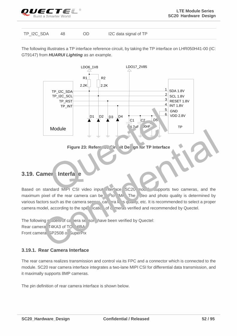
LTE Module Series SC20 Hardware Design
SC20_Hardware_Design Confidential / Released 52 / 95
TP_I2C_SDA 48 OD I2C data signal of TP
The following illustrates a TP interface reference circuit, by taking the TP interface on LHR050H41-00 (IC:
GT9147) from HUARUI Lighting as an example.
TP_RST
TP_I2C_SCL
TP_I2C_SDA
TP_INT
1
2
3
4
5
6
2.2K 2.2K
LDO17_2V85LDO6_1V8
4.7uF 100nFModule
RESET 1.8V
SCL 1.8V
SDA 1.8V
INT 1.8V
GND
VDD 2.8V
TP
R2R1
C1 C2D1 D2 D3 D4
D5
Figure 23: Reference Circuit Design for TP Interface
3.19. Camera Interface
Based on standard MIPI CSI video input interface, SC20 module supports two cameras, and the
maximum pixel of the rear camera can be up to 8MP. The video and photo quality is determined by
various factors such as the camera sensor, camera lens quality, etc. It is recommended to select a proper
camera model, according to the specification of cameras verified and recommended by Quectel.
The following models of camera sensors have been verified by Quectel:
Rear camera: T4KA3 of TOSHIBA
Front camera: SP2508 of SuperPix
3.19.1. Rear Camera Interface
The rear camera realizes transmission and control via its FPC and a connector which is connected to the
module. SC20 rear camera interface integrates a two-lane MIPI CSI for differential data transmission, and
it maximally supports 8MP cameras.
The pin definition of rear camera interface is shown below.
Quectel
Confidential

LTE Module Series SC20 Hardware Design
SC20_Hardware_Design Confidential / Released 53 / 95
Table 18: Pin Definition of Rear Camera Interface
Pin Name Pin No I/O Description Comment
LDO6_1V8 125 PO Power output 1.8V normal voltage
LDO17_2V85 129 PO Power output 2.85V normal voltage
MIPI_CSI0_CLKN 63 AI MIPI clock signal of rear
camera
MIPI_CSI0_CLKP 64 AI
MIPI_CSI0_LN0N 65 AI
MIPI data signal of rear
camera
MIPI_CSI0_LN0P 66 AI
MIPI_CSI0_LN1N 67 AI
MIPI_CSI0_LN1P 68 AI
CAM0_MCLK 74 DO Clock signal of rear
camera
CAM0_RST 79 DO Reset signal of rear
camera
CAM0_PWD 80 DO Power down signal of
rear camera
CAM_I2C_SCL 83 OD I2C clock signal of
camera
CAM_I2C_SDA 84 OD I2C data signal of
camera
The following is a reference circuit design for rear camera interface, by taking the connection with T4KA3
camera as an example.
Quectel
Confidential

LTE Module Series SC20 Hardware Design
SC20_Hardware_Design Confidential / Released 54 / 95
MIPI_CSI0_CLKP
DVDD_1V2
NC
AF_VDD2V8
DGND
NC
GND
SIOC
GND
CAM_I2C_SDA
MIPI_CSI0_LN1P
100nF
MIPI_CSI0_LN1N
CAM_I2C_SCL
CAM0_RST
MIPI_CSI0_CLKN
MIPI_CSI0_LN0P
MIPI_CSI0_LN0N
CAM0_PWD
CAM0_MCLK
NC
NC
MDP2
MDN2
GND
SIOD
RESET
AVDD_2V8
DOVDD1V8
DGND
MCP
MCN
MDP1
MDN1
DGND
NC
XCLK
1uF 1uF
DVDD_1V2
VDD_AF_2V8LDO6_1V8
LDO17_2V85
LDO6_1V8
0R_NM
0R
25
24
23
22
21
20
19
18
17
16
15
14
13
12
11
10
9
8
7
6
5
4
3
2
1
1
2
3
45 6
1
2
3
45 6
1
2
3
45 6
2.2K2.2K
ModuleRear Camera
FL1
FL2
FL3
EMI Filter
R1 R2
EMI Filter
C1 C2 C3
R3
R4
Figure 24: Reference Circuit Design for Rear Camera Interface
DVDD_1V2 is used to power the rear camera core, and VDD_AF_2V8 is used to power the rear camera
AF circuit. Both of them are powered by an external LDO.
3.19.2. Front Camera Interface
The front camera interface integrates a differential data interface meeting one-lane MIPI CSI standard,
and is tested to support 2MP cameras.
The pin definition of rear camera interface is shown below.
Table 19: Pin Definition of Front Camera Interface
Pin Name Pin No I/O Description Comment
LDO6_1V8 125 PO Power output 1.8V normal voltage
NOTE Quectel
Confidential

LTE Module Series SC20 Hardware Design
SC20_Hardware_Design Confidential / Released 55 / 95
LDO17_2V85 129 PO Power output 2.85V normal voltage
MIPI_CSI1_CLKN 70 AI MIPI clock signal of front
camera
MIPI_CSI1_CLKP 71 AI
MIPI_CSI1_LN0N 72 AI MIPI data signal of front
camera
MIPI_CSI1_LN0P 73 AI
CAM1_MCLK 75 DO Clock signal of front
camera
CAM1_RST 81 DO Reset signal of front
camera
CAM1_PWD 82 DO Power down signal of
front camera
CAM_I2C_SCL 83 OD I2C clock signal of
camera
CAM_I2C_SDA 84 OD I2C data signal of
camera
The following is a reference circuit design for front camera interface, by taking the connection with
SP2508 camera as an example.
MIPI_CSI1_CLKP
DGND
DGND
CLKP
CLKN
DGND
MDN0
DGND
MCLK
CAM_I2C_SDA
100nF
CAM_I2C_SCL
CAM1_RST
MIPI_CSI1_CLKN
MIPI_CSI1_LN0P
MIPI_CSI1_LN0N
CAM1_PWD
CAM1_MCLK
DGND
MDP0
DGND
DGND
NC(MDP1)
NC(MDN1)
DGND
DGND
SCL
SDA
PWDN
RST
AVDD2V8
AGND
DGND
DOVDD1V8
NC
1uF2.2uF
0R
LDO17_2V85
LDO6_1V8
1
2
3
4
5
6
7
8
9
10
11
12
13
14
15
16
17
18
19
20
21
22
23
24
25
100nF
2.2K 2.2K
1
2
3
45 6
1
2
3
45 6
LDO6_1V8
Module
Front Camera
FL2
FL1
R2R1
R3
C1 C2 C3 C4
EMI Filter
Figure 25: Reference Circuit Design for Front Camera Interface
Quectel
Confidential

LTE Module Series SC20 Hardware Design
SC20_Hardware_Design Confidential / Released 56 / 95
3.19.3. Design Considerations
Special attention should be paid to the definition of video device interface in schematic design.
Different video devices will have varied definitions for their corresponding connectors. Assure the
device and the connectors are correctly connected.
MIPI are high speed signal lines, supporting maximum data rate up to 1.5Gbps. The differential
impedance should be controlled as 100Ω. Additionally, it is recommended to route the trace on the
inner layer of PCB, and don’t cross it with other traces. For the same video device, all the MIPI traces
should keep the same length. In order to avoid crosstalk, a distance of 1.5 times of the trace width is
recommended to be maintained among MIPI signal lines. During impedance matching, don’t connect
GND on different planes so as to ensure impedance consistency.
It is recommended to select a low capacitance TVS for ESD protection and the recommended
parasitic capacitance is below 1pF.
Route MIPI traces according to the following rules:
1. The trace length should not exceed 305mm.
2. Control the differential impedance as 100Ω ±10%.
3. Control the length error of differential lines in the same lane within 0.67mm.
4. Control the length error of differential lines in different lanes within 1.3mm.
Table 20: MIPI Trace Length inside the Module
PIN Pin Name Length (mm) Length Difference (P-N)
52 MIPI_DSI_CLKN 7.08
-0.63
53 MIPI_DSI_CLKP 6.45
54 MIPI_DSI_LN0N 6.15
-0.30
55 MIPI_DSI_LN0P 5.85
56 MIPI_DSI_LN1N 6.64
-0.04
57 MIPI_DSI_LN1P 6.60
58 MIPI_DSI_LN2N 8.20
0.74
59 MIPI_DSI_LN2P 8.94
60 MIPI_DSI_LN3N 9.28
0.96
61 MIPI_DSI_LN3P 10.24
63 MIPI_CSI0_CLKN 10.55
0.54
64 MIPI_CSI0_CLKP 11.09
Quectel
Confidential

LTE Module Series SC20 Hardware Design
SC20_Hardware_Design Confidential / Released 57 / 95
65 MIPI_CSI0_LN0N 12.13
0.40
66 MIPI_CSI0_LN0P 12.53
67 MIPI_CSI0_LN1N 13.73
0.76
68 MIPI_CSI0_LN1P 14.49
70 MIPI_CSI1_CLKN 17.32
0.13
71 MIPI_CSI1_CLKP 17.45
72 MIPI_CSI1_LN0N 18.89
0.35
73 MIPI_CSI1_LN0P 19.24
3.20. Sensor Interface
SC20 module supports communication with sensors via I2C interface, and it supports ALS/PS, Compass,
G-sensor, and Gyroscopic sensors.
Verified sensor models by Quectel include: BST-BMA223, STK3311-WV, MPU-6881, and MMC35240PJ.
Table 21: Pin Definition of Sensor Interface
Pin Name Pin No I/O Description Comment
SENSOR_I2C_SCL 91 OD I2C clock signal for
external sensor
SENSOR_I2C_SDA 92 OD I2C data signal for
external sensor
GPIO_88 99 DI Gyroscope sensor
interrupt signal 2
Default configuration;
include but not limited to
these GPIO pins
GPIO_89 100 DI Gyroscope sensor
interrupt signal 1
GPIO_94 107 DI Proximity sensor interrupt
signal
GPIO_36 108 DI Compass sensor interrupt
signal
GPIO_65 109 DI Gravity sensor interrupt
signal 2
Quectel
Confidential

LTE Module Series SC20 Hardware Design
SC20_Hardware_Design Confidential / Released 58 / 95
GPIO_96 110 DI Gravity sensor interrupt
signal 1
3.21. Audio Interfaces
SC20 module provides two analog input channels and three analog output channels. The following table
shows the pin definition.
Table 22: Pin Definition of Audio Interface
Pin Name Pin No I/O Description Comment
MIC1P 4 AI Channel 1 microphone
positive input
MIC_GND 5 MIC reference GND
MIC2P 6 AI Channel 2 microphone
positive input
EARP 8 AO Earpiece positive output
EARN 9 AO Earpiece negative output
SPKP 10 AO Speaker positive output
SPKN 11 AO Speaker negative output
HPH_R 136 AO Headphone right channel
output
HPH_GND 137 Headphone virtual GND
HPH_L 138 AO Headphone left channel
output
HS_DET 139 AI Headset insertion
detection High level by default
The module offers two audio input channels which are both single-ended channels.
The earpiece interface uses differential output.
The loudspeaker interface uses differential output as well. The output channel is available with a
Class-D amplifier whose output power is 879mW when VBAT is 4.2V and load is 8Ω.
The headphone interface features stereo left and right channel output, and headphone insert
detection function is supported.
Quectel
Confidential

LTE Module Series SC20 Hardware Design
SC20_Hardware_Design Confidential / Released 59 / 95
3.21.1. Reference Circuit Design for Microphone
MIC1P
MIC_GND
0R
0R
33pF 100pF
MIC
NCF2
F1
C1
C2 C3
Module
D1
Figure 26: Reference Circuit Design for Microphone Interface
3.21.2. Reference Circuit Design for Receiver Interface
EARP
EARNF2
33pF
0R
0R
33pF
33pF
C2
C3
C1
F1
Module
D1 D2
Figure 27: Reference Circuit Design for Receiver Interface
Quectel
Confidential

LTE Module Series SC20 Hardware Design
SC20_Hardware_Design Confidential / Released 60 / 95
3.21.3. Reference Circuit Design for Headphone Interface
NM
0R
20K
ESD
MIC_GND
MIC2P
HPH_L
HS_DET
HPH_R
HPH_GND
33pF
0R
Module
C1
NM
C2
R1 R2
0R
R3
R4
0R
3645
2
1
33pF 33pF
C3 C4 C5
F3
F2
F1
D1 D2 D3 D4
0R
0R
0RF4
Figure 28: Reference Circuit Design for Headphone Interface
3.21.4. Reference Circuit Design for Loudspeaker Interface
EARP
EARNF2
SPKP
SPKN
0R
0R
33pF33pF
C1 C2
F1
Module
D1 D2
Figure 29: Reference Circuit Design for Loudspeaker Interface
3.21.5. Audio Interface Design Considerations
It is recommended to use the electret microphone with dual built-in capacitors (e.g. 10pF and 33pF) for
filtering out RF interference, thus reducing TDD noise. The 33pF capacitor is applied for filtering out
Quectel
Confidential

LTE Module Series SC20 Hardware Design
SC20_Hardware_Design Confidential / Released 61 / 95
900MHz RF interference when the module is transmitting at EGSM900MHz. Without placing this
capacitor, TDD noise could be heard. Moreover, the 10pF capacitor here is used for filtering out 1800MHz
RF interference. Please note that the resonant frequency point of a capacitor largely depends on the
material and production technique. Therefore, customers would have to discuss with their capacitor
vendors to choose the most suitable capacitor for filtering out high-frequency noises.
The severity degree of the RF interference in the voice channel during GSM transmitting period largely
depends on the application design. In some cases, GSM900 TDD noise is more severe; while in other
cases, DCS1800 TDD noise is more obvious. Therefore, a suitable capacitor can be selected based on
the test results. Sometimes, even no RF filtering capacitor is required.
The capacitor which is used for filtering out RF noise should be close to the audio device or audio
interface. The trace should be as short as possible, and it is recommended to route the trace for
capacitors first and then for other points.
In order to decrease radio or other signal interference, the position of RF antenna should be kept away
from audio interface and audio trace. Power trace couldn’t be parallel with audio trace and also should be
far away from the audio trace.
The differential audio traces must be routed according to the differential signal layout rule.
3.22. Emergency Download Interface
USB_BOOT is an emergency download interface. Pull up USB_BOOT to LDO5_1V8 with a 10K resistor
will make the module enter into emergency download mode, and this is the final option to be selected
when there are module failures such as abnormal startup or running. For convenience of firmware
upgrade and debugging in the future, please reverse this pin.
LDO5_1V8
S1
Module
USB_BOOTR1
10KD1
Figure 30: Reference Circuit Design for Emergency Download Interface
Quectel
Confidential

LTE Module Series SC20 Hardware Design
SC20_Hardware_Design Confidential / Released 62 / 95
4 Wi-Fi and BT
SC20 module provides a shared antenna interface ANT_WIFI/BT for Wi-Fi and Bluetooth (BT) functions.
The interface impedance is 50Ω. External antennas such as PCB antenna, sucker antenna and ceramic
antenna can be connected to the module via the interface, so as to achieve Wi-Fi and BT functions.
4.1. Wi-Fi Overview
SC20 module supports 2.4G single-band WLAN wireless communication based on IEEE 802.11 b/
802.11g/ 802.11n standard protocols. The maximum data rate is up to 150 Mbps.
The features are as below:
Support Wake-on-WLAN (WoWLAN)
Support ad hoc mode
Support WAPI SMS4 hardware encryption
Support AP mode
Support Wi-Fi Direct
Support MCS 0-7 for HT20 and HT40
4.1.1. Wi-Fi Performance
The following table lists the Wi-Fi transmitting and receiving performance of SC20 module.
Table 23: Wi-Fi Transmitting Performance
Standard Rate Output Power
802.11b 1Mbps 15.77dBm
802.11b 11Mbps 15.62dBm
802.11g 6Mbps 15.59dBm
802.11g 54Mbps 15.01dBm
Quectel
Confidential

LTE Module Series SC20 Hardware Design
SC20_Hardware_Design Confidential / Released 63 / 95
802.11n HT20 MCS0 13.97dBm
802.11n HT20 MCS7 13.08dBm
802.11n HT40 MCS0 14.75dBm
802.11n HT40 MCS7 13.52dBm
Table 24: Wi-Fi Receiving Performance
Standard Rate Sensitivity
802.11b 1/11Mbps -86dBm
802.11g 54Mbps -76dBm
802.11n HT20 MCS7 -74dBm
Referenced specifications are listed below:
No. Document
1 IEEE 802.11n WLAN MAC and PHY, October 2009 + IEEE 802.11-2007 WLAN MAC and
PHY, June 2007
2 IEEE Std 802.11b, IEEE Std 802.11d, IEEE Std 802.11e, IEEE Std 802.11g, IEEE Std
802.11i: IEEE 802.11-2007 WLAN MAC and PHY, June 2007
4.2. BT Overview
SC20 module supports BT4.1 (BR/EDR+BLE) specification, as well as GFSK, 8-DPSK, π/4-DQPSK
modulation modes.
Maximally support up to 7 wireless connections.
Maximally support up to 3.5 piconets at the same time.
Support one SCO (Synchronous Connection Oriented) or eSCO connection.
The BR/EDR channel bandwidth is 1MHz, and can accommodate 79 channels. The BLE channel
bandwidth is 2MHz, and can accommodate 40 channels.
Quectel
Confidential
LTE Module Series SC20 Hardware Design
SC20_Hardware_Design Confidential / Released 64 / 95
Table 25: BT Data Rate and Version
Version Data rate Maximum Application Throughput Comment
1.2 1 Mbit/s >80 Kbit/s
2.0 + EDR 3 Mbit/s >80 Kbit/s
3.0 + HS 24 Mbit/s Reference 3.0 + HS
4.0 24 Mbit/s Reference 4.0 LE
Referenced specifications are listed below:
No. Document
1 Bluetooth Radio Frequency TSS and TP Specification 1.2/2.0/2.0 + EDR/2.1/2.1+ EDR/3.0/3.0
+ HS, August 6, 2009
2 Bluetooth Low Energy RF PHY Test Specification, RF-PHY.TS/4.0.0, December 15, 2009
4.2.1. BT Performance
The following table lists the BT transmitting and receiving performance of SC20 module.
Table 26: BT Transmitting and Receiving Performance
Transmitter Performance
Packet Types DH5 2-DH5 3-DH5
Transmitting Power 10dBm 8dBm 8dBm
Receiver Performance
Packet Types DH5 2-DH5 3-DH5
Receiving Sensitivity -93dBm -92dBm -86dBm
Quectel
Confidential

LTE Module Series SC20 Hardware Design
SC20_Hardware_Design Confidential / Released 65 / 95
5 GNSS
SC20 module integrates a Qualcomm IZat™ GNSS engine (GEN 8C) which supports multiple positioning
and navigation systems including GPS, GLONASS and BeiDou. With an embedded LNA, the module
provides greatly improved positioning accuracy.
5.1. GNSS Performance
The following table lists the GNSS performance of SC20 module in conduction mode.
Table 27: GNSS Performance
Parameter Description Typ. Unit
Sensitivity (GNSS)
Cold start -146 dBm
Reacquisition -158 dBm
Tracking -160 dBm
TTFF (GNSS)
Cold start 32 s
Warm start 30 s
Hot start 2 s
Static Drift (GNSS) CEP-50 6 m
5.2. GNSS RF Design Guidance
Bad design of antenna and layout may cause reduced GPS receiving sensitivity, longer GPS positioning
time, or reduced positioning accuracy. In order to avoid this, please follow the reference design rules as
below:
Quectel
Confidential

LTE Module Series SC20 Hardware Design
SC20_Hardware_Design Confidential / Released 66 / 95
Maximize the distance between the GNSS RF part and the GPRS RF part (including trace routing
and antenna layout) to avoid mutual interference.
In user systems, GNSS RF signal lines and RF components should be placed far away from high
speed circuits, switched-mode power supplies, power inductors, the clock circuit of single-chip
microcomputers, etc.
For applications with harsh electromagnetic environment or with high requirement on ESD protection,
it is recommended to add ESD protective diodes for the antenna interface. Only diodes with ultra-low
junction capacitance such as 0.5pF can be selected. Otherwise, there will be effects on the
impedance characteristic of RF circuit loop, or attenuation of bypass RF signal may be caused.
Control the impedance of either feeder line or PCB trace as 50Ω, and keep the trace length as short
as possible.
Refer to Chapter 6.3 for GNSS reference circuit design.
Quectel
Confidential

LTE Module Series SC20 Hardware Design
SC20_Hardware_Design Confidential / Released 67 / 95
6 Antenna Interface
SC20 antenna interface includes a main antenna, an Rx-diversity/MIMO antenna, a GNSS antenna and a
Wi-Fi/BT antenna. The antenna interface has an impedance of 50Ω.
6.1. Main/Rx-diversity Antenna Interface
6.1.1. Pin Definition
The main antenna and Rx-diversity antenna pins’ definition are shown below.
Table 28: Pin Definition of the Main/Rx-diversity Antenna
Pin Name Pin No. I/O Description Comment
ANT_MAIN 87 IO Main antenna 50Ω impedance
ANT_DRX 131 AI Diversity antenna 50Ω impedance
6.1.2. Operating Frequency
Table 29: SC20 Module Operating Frequencies
3GPP Band Receive Transmit Unit
EGSM900 925-960 880-915 MHz
DCS1800 1805-1880 1710-1785 MHz
WCDMA Band 1 2110-2170 1920-1980 MHz
WCDMA Band 8 925-960 880-915 MHz
CDMA BC0 869-894 824-849 MHz
TD-SCDMA Band 34 2010-2025 2010-2025 MHz
Quectel
Confidential

LTE Module Series SC20 Hardware Design
SC20_Hardware_Design Confidential / Released 68 / 95
TD-SCDMA Band 39 1880-1920 1880-1920 MHz
LTE-FDD Band 1 2110-2170 1920-1980 MHz
LTE-FDD Band 3 1805-1880 1710-1785 MHz
LTE-FDD Band 8 925-960 880-915 MHz
LTE-FDD Band 38 2570-2620 2570-2620 MHz
LTE-FDD Band 39 1880-1920 1880-1920 MHz
LTE-FDD Band 40 2300-2400 2300-2400 MHz
LTE-FDD Band 41 2555-2655 2555-2655 MHz
The bandwidth of LTE-TDD Band 41 for SC20 module is 100MHz (2555 MHz - 2655 MHz), and the
corresponding channel range is from 40240 up to 41240.
6.1.3. Main and Rx-diversity Antenna Reference Design
A reference circuit design for ANT_MAIN and ANT_DRX antenna is shown as below. A π-type matching
circuit should be reserved for better RF performance. The capacitors are not mounted by default.
ANT_MAIN
R1 0R
C1
Module
Main
antenna
NM
C2
NM
R2 0R
C3
DRX
antenna
NM
C4
NM
ANT_DRX
Figure 31: Reference Circuit Design for Main and Rx-diversity Antenna
NOTE
Quectel
Confidential

LTE Module Series SC20 Hardware Design
SC20_Hardware_Design Confidential / Released 69 / 95
6.2. Wi-Fi/BT Antenna Interface
The following tables show the Wi-Fi/BT antenna pin’s definition and frequency specification.
Table 30: Pin Definition of Wi-Fi/BT Antenna
Pin Name Pin No. I/O Description Comment
ANT_WIFI/BT 77 IO Wi-Fi/BT antenna 50Ω impedance
Table 31: Wi-Fi/BT Frequency
Type Frequency Unit
802.11b/g/n 2402~2482 MHz
BT4.1 LE 2402~2480 MHz
A reference circuit design for Wi-Fi/BT antenna is shown as below. A π-type matching circuit should be
reserved for better RF performance. The capacitors are not mounted by default.
ANT_WIFI/BTR1 0R
C1
Module
2.4G
antenna
NM
C2
NM
Figure 32: Reference Circuit Design for Wi-Fi/BT Anternna
6.3. GNSS Antenna Interface
The following tables show the GNSS antenna pin’s definition and frequency specification.
Quectel
Confidential
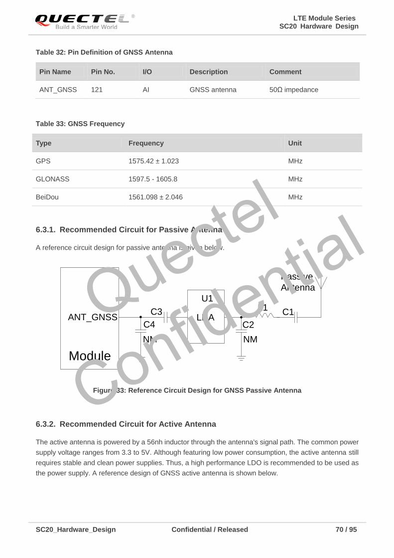
LTE Module Series SC20 Hardware Design
SC20_Hardware_Design Confidential / Released 70 / 95
Table 32: Pin Definition of GNSS Antenna
Pin Name Pin No. I/O Description Comment
ANT_GNSS 121 AI GNSS antenna 50Ω impedance
Table 33: GNSS Frequency
Type Frequency Unit
GPS 1575.42 ± 1.023 MHz
GLONASS 1597.5 - 1605.8 MHz
BeiDou 1561.098 ± 2.046 MHz
6.3.1. Recommended Circuit for Passive Antenna
A reference circuit design for passive antenna is given below.
LNA
Passive
Antenna
Module
ANT_GNSS
NM
C1
C2
L1U1
C3
C4
NM
Figure 33: Reference Circuit Design for GNSS Passive Antenna
6.3.2. Recommended Circuit for Active Antenna
The active antenna is powered by a 56nh inductor through the antenna's signal path. The common power
supply voltage ranges from 3.3 to 5V. Although featuring low power consumption, the active antenna still
requires stable and clean power supplies. Thus, a high performance LDO is recommended to be used as
the power supply. A reference design of GNSS active antenna is shown below.
Quectel
Confidential

LTE Module Series SC20 Hardware Design
SC20_Hardware_Design Confidential / Released 71 / 95
Active Antenna3V3
Module
ANT_GNSS
56nH
10R
1uF
100pF
NMNM
C4
C1
R1
L1
R2
0R C5
C3
C2
100pF
Figure 34: Reference Circuit Design for GNSS Active Antenna
6.4. Antenna Installation
6.4.1. Antenna Requirement
The following table shows the requirement on main antenna, RX-diversity antenna, Wi-Fi/BT antenna and
GNSS antenna.
Table 34: Antenna Requirements
Type Requirements
GSM/WCDMA/TD-SCDMA/LTE
VSWR: ≤ 2
Gain (dBi): 1
Max Input Power (W): 50
Input Impedance (Ω): 50
Polarization Type: Vertical
Cable Insertion Loss: < 1dB (GSM900, WCDMA B8, LTE B8)
Cable Insertion Loss: < 1.5dB
(DCS1800, WCDMA B1, TD-SCDMA B34/B39, LTE B1/3/39)
Cable Insertion Loss: < 2dB (LTE B38/40/41)
Wi-Fi/BT
VSWR: ≤ 2
Gain (dBi): 1
Max Input Power (W): 50
Input Impedance (Ω): 50
Polarization Type: Vertical
Cable Insertion Loss: < 1dB
GNSS Frequency range: 1565 - 1607MHz
Polarization: RHCP or linear
Quectel
Confidential

LTE Module Series SC20 Hardware Design
SC20_Hardware_Design Confidential / Released 72 / 95
VSWR: < 2 (Typ.)
Passive Antenna Gain: > 0dBi
Active Antenna Noise Figure: < 1.5dB
Active Antenna Gain: > -2dBi
Active Antenna Embedded LNA Gain: 20dB (Typ.)
Active Antenna Total Gain: > 18dBi (Typ.)
6.4.2. Install the Antenna with RF Connector
The following figure shows the antenna installation with RF connector provided by HIROSE. The
recommended RF connector is UF.L-R-SMT.
Figure 35: Dimensions of the UF.L-R-SMT Connector (Unit: mm)
U.FL-LP serial connector listed in the following figure can be used to match the UF.L-R-SMT.
Quectel
Confidential
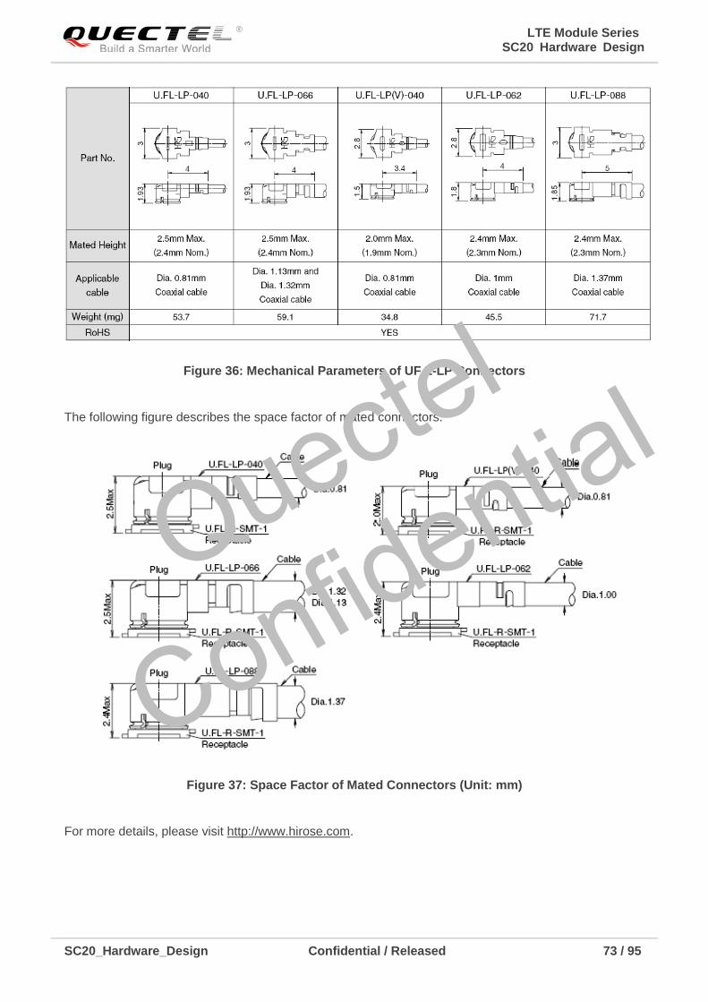
LTE Module Series SC20 Hardware Design
SC20_Hardware_Design Confidential / Released 73 / 95
Figure 36: Mechanical Parameters of UF.L-LP Connectors
The following figure describes the space factor of mated connectors.
Figure 37: Space Factor of Mated Connectors (Unit: mm)
For more details, please visit http://www.hirose.com.
Quectel
Confidential

LTE Module Series SC20 Hardware Design
SC20_Hardware_Design Confidential / Released 74 / 95
7 Electrical, Reliability and Radio
Characteristics
7.1. Absolute Maximum Ratings
Absolute maximum ratings for power supply and voltage on digital and analog pins of the module are
listed in the following table.
Table 35: Absolute Maximum Ratings
Parameter Min. Max. Unit
VBAT -0.5 6 V
USB_VBUS -0.5 16 V
Peak Current of VBAT 0 3 A
Voltage on Digital Pins -0.3 2.3 V
7.2. Power Supply Ratings
Table 36: SC20 Module Power Supply Ratings
Parameter Description Conditions Min. Typ. Max. Unit
VBAT
VBAT
Voltage must stay within the
min/max values, including
voltage drop, ripple and spikes.
3.5 3.8 4.2 V
Voltage drop
during transmitting
burst
Maximum power control level
on EGSM900. 400 mV
IVBAT Peak supply Maximum power control level 1.8 3.0 A
Quectel
Confidential

LTE Module Series SC20 Hardware Design
SC20_Hardware_Design Confidential / Released 75 / 95
Parameter Description Conditions Min. Typ. Max. Unit
current (during
transmission slot)
on EGSM900.
USB_VBUS USB detection 4.35 5.0 6.3 V
VRTC
Power supply
voltage of backup
battery.
2.0 3.0 3.25 V
7.3. Charging Performance Specifications
Table 37: Charging Performance Specifications
Parameter Min. Typ. Max. Unit
Trickle charging-A current 81 90 99 mA
Trickle charging-A threshold voltage
range (15.62mV steps) 2.5 2.796 2.984 V
Trickle charging-B threshold voltage
range (18.75mV steps) 3.0 3.2 3.581 V
Charge voltage range (25mV steps) 4 4.2 4.775 V
Charge voltage accuracy +/-2 %
Charge current range (90mA steps) 90 1440 mA
Charge current accuracy +/-10 %
Charge termination current: when charge
current is from 90 to 450mA; 7 %
Charge termination current: when charge
current is from 450 to 1440mA; 7.4 %
7.4. Operating Temperature
The operating temperature is listed in the following table.
Quectel
Confidential

LTE Module Series SC20 Hardware Design
SC20_Hardware_Design Confidential / Released 76 / 95
Table 38: Operating Temperature
Parameter Min. Typ. Max. Unit
Operating temperature range 1)
-35 +25 +75 ºC
Extended temperature range 2)
-40 +85 ºC
1. 1)
Operating temperature range ---- 3GPP compliant.
2. 2)
Within extended temperature range, the module remains the ability to establish and maintain a
voice, SMS, data transmission, emergency call, etc. There is no unrecoverable malfunction. There
are also no effects on radio spectrum and no harm to radio network. Only one or more parameters
like Pout might reduce in their value and exceed the specified tolerances. When the temperature
returns to the normal operating temperature levels, the module will meet 3GPP compliant again.
7.5. Current Consumption
The values of current consumption are shown below.
Table 39: SC20 Current Consumption
Parameter Description Conditions Min. Typ. Max. Unit
IVBAT
OFF state Power down 20 uA
GSM/GPRS
supply current
Sleep (USB disconnected)
@DRX=2 3.78 mA
Sleep (USB disconnected)
@DRX=5 2.59 mA
Sleep (USB disconnected)
@DRX=9 2.32 mA
WCDMA
supply current
Sleep (USB disconnected)
@DRX=6 3.21 mA
Sleep (USB disconnected)
@DRX=8 2.49 mA
Sleep (USB disconnected)
@DRX=9 2.12 mA
LTE-FDD
supply current Sleep (USB disconnected)
@DRX=6 3.79 mA
NOTES
Quectel
Confidential

LTE Module Series SC20 Hardware Design
SC20_Hardware_Design Confidential / Released 77 / 95
Parameter Description Conditions Min. Typ. Max. Unit
Sleep (USB disconnected)
@DRX=8 2.92 mA
Sleep (USB disconnected)
@DRX=9 2.53 mA
LTE-TDD
supply current
Sleep (USB disconnected)
@DRX=6 3.69 mA
Sleep (USB disconnected)
@DRX=8 2.83 mA
Sleep (USB disconnected)
@DRX=9 2.45 mA
GSM voice call
EGSM900 @PCL5 258 mA
EGSM900 @PCL12 134 mA
EGSM900 @PCL19 111 mA
DCS1800 @PCL0 210 mA
DCS1800 @PCL7 146 mA
DCS1800 @PCL15 129 mA
WCDMA voice call
Band 1 @max power 456 mA
Band 8 @max power 455 mA
GPRS data transfer
GPRS900 (1UL/4DL) @PCL5 246 mA
GPRS900 (2UL/3DL) @PCL5 399 mA
GPRS900 (3UL/2DL) @PCL5 480 mA
GPRS900 (4UL/1DL) @PCL5 555 mA
DCS1800 (1UL/4DL) @PCL0 215 mA
DCS1800 (2UL/3DL) @PCL0 325 mA
DCS1800 (3UL/2DL) @PCL0 435 mA
DCS1800 (4UL/1DL) @PCL0 550 mA
EDGE data transfer
EDGE900 (1UL/4DL) @PCL8 189 mA
EDGE900 (2UL/3DL) @PCL8 277 mA
Quectel
Confidential

LTE Module Series SC20 Hardware Design
SC20_Hardware_Design Confidential / Released 78 / 95
Parameter Description Conditions Min. Typ. Max. Unit
EDGE900 (3UL/2DL) @PCL8 375 mA
EDGE900 (4UL/1DL) @PCL8 471 mA
DCS1800 (1UL/4DL) @PCL2 185 mA
DCS1800 (2UL/3DL) @PCL2 269 mA
DCS1800 (3UL/2DL) @PCL2 366 mA
DCS1800 (4UL/1DL) @PCL2 466 mA
WCDMA
data transfer
Band 1(HSDPA) @max power 455 mA
Band 8(HSDPA) @max power 436 mA
LTE
data transfer
LTE-FDD Band1 @max power 713 mA
LTE-FDD Band3 @max power 736 mA
LTE-FDD Band8 @max power 715 mA
LTE-TDD Band38 @max power 354 mA
LTE-TDD Band39 @max power 391 mA
LTE-TDD Band40 @max power 392 mA
LTE-TDD Band41 @max power 372 mA
7.6. RF Output Power
The following table shows the RF output power of SC20 module.
Table 40: RF Output Power
Frequency Max. Min.
EGSM900 33dBm±2dB 5dBm±5dB
DCS1800 30dBm±2dB 0dBm±5dB
WCDMA Band1 24dBm+1/-3dB <-50dBm
Quectel
Confidential

LTE Module Series SC20 Hardware Design
SC20_Hardware_Design Confidential / Released 79 / 95
WCDMA Band8 24dBm+1/-3dB <-50dBm
CDMA BC0 24dBm+3/-1dB <-50dBm
TD-SCDMA Band34 24dBm+1/-3dB <-50dBm
TD-SCDMA Band39 24dBm+1/-3dB <-50dBm
LTE-FDD B1 23dBm±2dB <-44dBm
LTE-FDD B3 23dBm±2dB <-44dBm
LTE-FDD B8 23dBm±2dB <-44dBm
LTE-TDD B38 23dBm±2dB <-44dBm
LTE-TDD B39 23dBm±2dB <-44dBm
LTE-TDD B40 23dBm±2dB <-44dBm
LTE-TDD B41 23dBm±2dB <-44dBm
In GPRS 4 slots TX mode, the maximum output power is reduced by 3dB. This design conforms to the
GSM specification as described in Chapter 13.16 of 3GPP TS 51.010-1.
7.7. RF Receiving Sensitivity
The following table shows the RF receiving sensitivity of SC20 module.
Table 41: RF Receiving Sensitivity
Frequency Receive Sensitivity (Typ.)
Primary Diversity SIMO 3GPP(SIMO)
EGSM900 -109dBm NA NA -104dBm
DCS1800 -109dBm NA NA -104dBm
WCDMA Band1 -110dBm NA NA -106.7dBm
WCDMA Band8 -110dBm NA NA -103.7dBm
NOTE
Quectel
Confidential

LTE Module Series SC20 Hardware Design
SC20_Hardware_Design Confidential / Released 80 / 95
CDMA BC0 -110 dBm NA NA -104dBm
TD-SCDMA
Band 34 -109 dBm NA NA -108dBm
TD-SCDMA
Band 39 -109 dBm NA NA -108dBm
LTE-FDD B1 -98 dBm -99 dBm -102 dBm -96.3dBm
LTE-FDD B3 -97 dBm -98 dBm -101 dBm -93.3dBm
LTE-FDD B8 -97 dBm -98 dBm -101 dBm -93.3dBm
LTE-FDD B38 -97 dBm -98 dBm -100 dBm -96.3dBm
LTE-FDD B39 -98 dBm -98 dBm -101 dBm -96.3dBm
LTE-FDD B40 -97 dBm -98 dBm -100 dBm -96.3dBm
LTE-FDD B41 -96 dBm -98 dBm -100 dBm -94.3dBm
7.8. Electrostatic Discharge
The module is not protected against electrostatic discharge (ESD) in general. Consequently, it should be
subject to ESD handling precautions that are typically applied to ESD sensitive components. Proper ESD
handling and packaging procedures must be applied throughout the processing, handling and operation
of any application that incorporates the module.
The following table shows the module electrostatic discharge characteristics.
Table 42: Electrostatic Discharge Characteristics ( Temperature: 25℃, Humidity: 45%)
Tested Points Contact Discharge Air Discharge Unit
VBAT, GND +/-5 +/-10 KV
All Antenna Interfaces +/-5 +/-10 KV
USB Interfaces +/-2 +/-4 KV
Other Interfaces +/-0.5 +/-1 KV
Quectel
Confidential

LTE Module Series SC20 Hardware Design
SC20_Hardware_Design Confidential / Released 81 / 95
8 Mechanical Dimensions
This chapter describes the mechanical dimensions of the module. All dimensions are measured in mm.
8.1. Mechanical Dimensions of the Module
Figure 38: Module Top and Side Dimensions
Quectel
Confidential

LTE Module Series SC20 Hardware Design
SC20_Hardware_Design Confidential / Released 82 / 95
Figure 39: Module Bottom Dimensions (Top View)
Quectel
Confidential
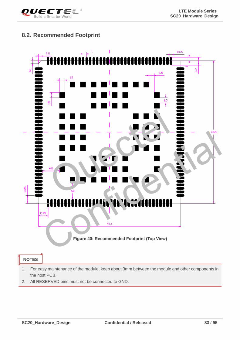
LTE Module Series SC20 Hardware Design
SC20_Hardware_Design Confidential / Released 83 / 95
8.2. Recommended Footprint
Figure 40: Recommended Footprint (Top View)
1. For easy maintenance of the module, keep about 3mm between the module and other components in
the host PCB.
2. All RESERVED pins must not be connected to GND.
NOTES
Quectel
Confidential

LTE Module Series SC20 Hardware Design
SC20_Hardware_Design Confidential / Released 84 / 95
8.3. Top and Bottom View of the Module
Figure 41: Top View of the Module
Figure 42: Bottom View of the Module
These are design effect drawings of SC20 module. For more accurate pictures, please refer to the
module that you get from Quectel.
NOTE
Quectel
Confidential

LTE Module Series SC20 Hardware Design
SC20_Hardware_Design Confidential / Released 85 / 95
9 Storage, Manufacturing and
Packaging
9.1. Storage
SC20 is stored in a vacuum-sealed bag. The restrictions of storage condition are shown as below.
1. Shelf life in sealed bag is 12 months at < 40ºC/90%RH.
2. After this bag is opened, devices that will be subjected to reflow soldering or other high temperature
process must be:
Mounted within 72 hours at factory conditions of ≤ 30ºC/60%RH.
Stored at < 10% RH.
3. Devices require baking before mounting, if:
Humidity indicator card is > 10% when ambient temperature is 23ºC±5ºC.
Mounting cannot be finished within 72 hours at factory conditions of ≤ 30ºC/60% RH.
4. If baking is required, devices may be baked for 48 hours at 125ºC±5ºC.
As plastic package cannot be subjected to high temperatures, the package must be removed from
devices before high temperature (125ºC) baking. If shorter baking time is desired, please refer to
IPC/JEDECJ-STD-033 for baking procedure.
9.2. Manufacturing and Welding
Push the squeegee to apply the solder paste on the surface of stencil, thus making the paste fill the
stencil openings and then penetrate to the PCB. The force on the squeegee should be adjusted properly
so as to produce a clean stencil surface on a single pass. To ensure the module soldering quality, the
thickness of stencil at the hole of the module pads should be 0.18mm. For details, please refer to
NOTE
Quectel
Confidential

LTE Module Series SC20 Hardware Design
SC20_Hardware_Design Confidential / Released 86 / 95
document [4].
It is suggested that the peak reflow temperature is from 235 to 245ºC (for SnAg3.0Cu0.5 alloy). The
absolute maximum reflow temperature is 260ºC. To avoid damage to the module caused by repeated
heating, it is suggested that the module should be mounted after reflow soldering for the other side of
PCB has been completed. Recommended reflow soldering thermal profile is shown below:
Time
50 100 150 200 250 300
50
100
150
200
250
160 ºC
200 ºC
217
0
70s~120s
40s~60s
Between 1~3 ºC/s
Preheat Heating CoolingºC
s
Liquids Temperature
Te
mp
era
ture
Figure 43: Reflow Soldering Thermal Profile
9.3. Packaging
SC20 is packaged in tape and reel carriers. One reel is 12.32 meters long and contains 200pcs modules.
The following figures show the package details, measured in mm.
Quectel
Confidential

LTE Module Series SC20 Hardware Design
SC20_Hardware_Design Confidential / Released 87 / 95
Figure 44: Tape Dimensions
Figure 45: Reel Dimensions
Quectel
Confidential

LTE Module Series SC20 Hardware Design
SC20_Hardware_Design Confidential / Released 88 / 95
Table 43: Reel Packaging
Model
Name MOQ for MP Minimum Package: 200pcs Minimum Package×4=800pcs
SC20 200
Size: 370mm*350mm*85mm
N.W: 1.92kg
G.W: 3.17kg
Size: 380mm*365mm*365mm
N.W:7.68 kg
G.W:13.63 kg
Quectel
Confidential

LTE Module Series SC20 Hardware Design
SC20_Hardware_Design Confidential / Released 89 / 95
10 Appendix A References
Table 44: Related Documents
SN Document Name Remark
[1] Quectel_SC20_AT_Commands_Manual SC20 AT Commands Manual
[2] Quectel_Smart_EVB_User_Guide Smart Module EVB User Guide
[3] Quectel_SC20_Reference_Design SC20 Reference Design
[4] Quectel_Module_Secondary_SMT_User_
Guide Module Secondary SMT User Guide
Table 45: Terms and Abbreviations
Abbreviation Description
ADC Analog-to-Digital Converter
AMR Adaptive Multi-rate
ARP Antenna Reference Point
bps Bits Per Second
CHAP Challenge Handshake Authentication Protocol
CS Coding Scheme
CSD Circuit Switched Data
CTS Clear to Send
DRX Discontinuous Reception
DCE Data Communications Equipment (typically module)
DTE Data Terminal Equipment (typically computer, external controller)
Quectel
Confidential

LTE Module Series SC20 Hardware Design
SC20_Hardware_Design Confidential / Released 90 / 95
DTR Data Terminal Ready
DTX Discontinuous Transmission
EFR Enhanced Full Rate
EGSM Extended GSM900 band (includes standard GSM900 band)
eSCD Enhanced Synchronous Connection Oriented
ESD Electrostatic Discharge
FR Full Rate
FPC Flexible Printed Circuit
GMSK Gaussian Minimum Shift Keying
GPS Global Positioning System
GSM Global System for Mobile Communications
HR Half Rate
HSPA High Speed Packet Access
I/O Input/Output
IMEI International Mobile Equipment Identity
Imax Maximum Load Current
Inorm Normal Current
LED Light Emitting Diode
LNA Low Noise Amplifier
MO Mobile Originated
MS Mobile Station (GSM engine)
MT Mobile Terminated
PAP Password Authentication Protocol
PBCCH Packet Broadcast Control Channel
PCB Printed Circuit Board
Quectel
Confidential

LTE Module Series SC20 Hardware Design
SC20_Hardware_Design Confidential / Released 91 / 95
PDU Protocol Data Unit
PPP Point-to-Point Protocol
PSK Phase Shift Keying
QAM Quadrature Amplitude Modulation
QPSK Quadrature Phase Shift Keying
RF Radio Frequency
RHCP Right Hand Circularly Polarized
RMS Root Mean Square (value)
RTC Real Time Clock
Rx Receive
SDIO Secure Digital Input and Output
SIM Subscriber Identification Module
SMS Short Message Service
TDMA Time Division Multiple Access
TE Terminal Equipment
TP Touch Panel
TX Transmitting Direction
UART Universal Asynchronous Receiver & Transmitter
UMTS Universal Mobile Telecommunications System
URC Unsolicited Result Code
USIM Universal Subscriber Identity Module
USSD Unstructured Supplementary Service Data
Vmax Maximum Voltage Value
Vnorm Normal Voltage Value
Vmin Minimum Voltage Value
Quectel
Confidential

LTE Module Series SC20 Hardware Design
SC20_Hardware_Design Confidential / Released 92 / 95
VIHmax Maximum Input High Level Voltage Value
VIHmin Minimum Input High Level Voltage Value
VILmax Maximum Input Low Level Voltage Value
VILmin Minimum Input Low Level Voltage Value
VImax Absolute Maximum Input Voltage Value
VImin Absolute Minimum Input Voltage Value
VOHmax Maximum Output High Level Voltage Value
VOHmin Minimum Output High Level Voltage Value
VOLmax Maximum Output Low Level Voltage Value
VOLmin Minimum Output Low Level Voltage Value
VSWR Voltage Standing Wave Ratio
WCDMA Wideband Code Division Multiple Access
Quectel
Confidential

LTE Module Series SC20 Hardware Design
SC20_Hardware_Design Confidential / Released 93 / 95
11 Appendix B GPRS Coding Schemes
Table 46: Description of Different Coding Schemes
Scheme CS-1 CS-2 CS-3 C4-4
Code Rate 1/2 2/3 3/4 1
USF 3 3 3 3
Pre-coded USF 3 6 6 12
Radio Block excl.USF and BCS 181 268 312 428
BCS 40 16 16 16
Tail 4 4 4 -
Coded Bits 456 588 676 456
Punctured Bits 0 132 220 -
Data Rate Kb/s 9.05 13.4 15.6 21.4
Quectel
Confidential

LTE Module Series SC20 Hardware Design
SC20_Hardware_Design Confidential / Released 94 / 95
12 Appendix C GPRS Multi-slot Classes
Twenty-nine classes of GPRS multi-slot modes are defined for MS in GPRS specification. Multi-slot
classes are product dependent, and determine the maximum achievable data rates in both the uplink and
downlink directions. Written as 3+1 or 2+2, the first number indicates the amount of downlink timeslots,
while the second number indicates the amount of uplink timeslots. The active slots determine the total
number of slots the GPRS device can use simultaneously for both uplink and downlink communications.
The description of different multi-slot classes is shown in the following table.
Table 47: GPRS Multi-slot Classes
Multislot Class Downlink Slots Uplink Slots Active Slots
1 1 1 2
2 2 1 3
3 2 2 3
4 3 1 4
5 2 2 4
6 3 2 4
7 3 3 4
8 4 1 5
9 3 2 5
10 4 2 5
11 4 3 5
12 4 4 5
Quectel
Confidential

LTE Module Series SC20 Hardware Design
SC20_Hardware_Design Confidential / Released 95 / 95
13 Appendix D EDGE Modulation and
Coding Schemes
Table 48: EDGE Modulation and Coding Schemes
Coding Scheme Modulation Coding Family 1 Timeslot 2 Timeslot 4 Timeslot
CS-1 GMSK / 9.05kbps 18.1kbps 36.2kbps
CS-2 GMSK / 13.4kbps 26.8kbps 53.6kbps
CS-3 GMSK / 15.6kbps 31.2kbps 62.4kbps
CS-4 GMSK / 21.4kbps 42.8kbps 85.6kbps
MCS-1 GMSK C 8.80kbps 17.60kbps 35.20kbps
MCS-2 GMSK B 11.2kbps 22.4kbps 44.8kbps
MCS-3 GMSK A 14.8kbps 29.6kbps 59.2kbps
MCS-4 GMSK C 17.6kbps 35.2kbps 70.4kbps
MCS-5 8-PSK B 22.4kbps 44.8kbps 89.6kbps
MCS-6 8-PSK A 29.6kbps 59.2kbps 118.4kbps
MCS-7 8-PSK B 44.8kbps 89.6kbps 179.2kbps
MCS-8 8-PSK A 54.4kbps 108.8kbps 217.6kbps
MCS-9 8-PSK A 59.2kbps 118.4kbps 236.8kbps
Quectel
Confidential