
SBS 1.1-COMPLIANT FUEL GAUGE WITH ADDITIONAL DQ … · bq34z950 slusbf0a – april 2013–revised...
30
bq34z950 www.ti.com SLUSBF0A – APRIL 2013 – REVISED MAY 2013 SBS 1.1-COMPLIANT GAS GAUGE AND PROTECTION ENABLED WITH IMPEDANCE TRACK™ WITH OPTIONAL DQ INTERFACE Check for Samples: bq34z950 1FEATURES APPLICATIONS 2• Next Generation Patented Impedance Track™ • Notebook PCs Technology Accurately Measures Available • Medical and Test Equipment Charge in Li-Ion and Li-Polymer Batteries • Portable Instrumentation – Better Than 1% Error Over the Lifetime of the Battery DESCRIPTION • Supports the Smart Battery Specification The bq34z950 SBS-compliant gas gauge and SBS V1.1 protection IC, incorporating patented Impedance Track technology, is a single IC solution designed for • Optional DQ Communication Interface battery-pack or in-system installation. The bq34z950 • Flexible Configuration for 2-Series to 4-Series measures and maintains an accurate record of Li-Ion and Li-Polymer Cells available charge in Li-Ion or Li-Polymer batteries • Powerful 8-Bit RISC CPU with Ultralow Power using its integrated high-performance analog peripherals. The bq34z950 monitors capacity change, Modes battery impedance, open-circuit voltage, and other • Full Array of Programmable Protection critical parameters of the battery pack which reports Features the information to the system host controller over a – Voltage serial-communication bus. SMBus and single-wire DQ communication interfaces are both available. – Current Together with the integrated analog front-end (AFE) – Temperature short-circuit and overload protection, the bq34z950 • Satisfies JEITA Guidelines maximizes functionality and safety while minimizing external component count, cost, and size in smart • Added Flexibility to Handle More Complex battery circuits. Charging Profiles • Drives 3-, 4-, and 5-Segment LED Display for The implemented Impedance Track gas gauging Battery-Pack Conditions technology continuously analyzes the battery impedance, resulting in superior gas-gauging • Supports SHA-1 Authentication accuracy. This enables remaining capacity to be • Complete Battery Protection and Gas Gauge calculated with discharge rate, temperature, and cell Solution in One Package aging all accounted for during each stage of every • Available in a 44-Pin TSSOP (DBT) Package cycle with high accuracy. 1 Please be aware that an important notice concerning availability, standard warranty, and use in critical applications of Texas Instruments semiconductor products and disclaimers thereto appears at the end of this data sheet. 2Impedance Track is a trademark of Texas Instruments. PRODUCTION DATA information is current as of publication date. Copyright © 2013, Texas Instruments Incorporated Products conform to specifications per the terms of the Texas Instruments standard warranty. Production processing does not necessarily include testing of all parameters.
Transcript of SBS 1.1-COMPLIANT FUEL GAUGE WITH ADDITIONAL DQ … · bq34z950 slusbf0a – april 2013–revised...

bq34z950
www.ti.com SLUSBF0A – APRIL 2013–REVISED MAY 2013
SBS 1.1-COMPLIANT GAS GAUGE AND PROTECTIONENABLED WITH IMPEDANCE TRACK™ WITH OPTIONAL DQ INTERFACE
Check for Samples: bq34z950
1FEATURES APPLICATIONS2• Next Generation Patented Impedance Track™ • Notebook PCs
Technology Accurately Measures Available • Medical and Test EquipmentCharge in Li-Ion and Li-Polymer Batteries • Portable Instrumentation– Better Than 1% Error Over the Lifetime of
the Battery DESCRIPTION• Supports the Smart Battery Specification The bq34z950 SBS-compliant gas gauge and
SBS V1.1 protection IC, incorporating patented ImpedanceTrack technology, is a single IC solution designed for• Optional DQ Communication Interfacebattery-pack or in-system installation. The bq34z950
• Flexible Configuration for 2-Series to 4-Series measures and maintains an accurate record ofLi-Ion and Li-Polymer Cells available charge in Li-Ion or Li-Polymer batteries
• Powerful 8-Bit RISC CPU with Ultralow Power using its integrated high-performance analogperipherals. The bq34z950 monitors capacity change,Modesbattery impedance, open-circuit voltage, and other• Full Array of Programmable Protectioncritical parameters of the battery pack which reportsFeaturesthe information to the system host controller over a
– Voltage serial-communication bus. SMBus and single-wireDQ communication interfaces are both available.– CurrentTogether with the integrated analog front-end (AFE)– Temperatureshort-circuit and overload protection, the bq34z950
• Satisfies JEITA Guidelines maximizes functionality and safety while minimizingexternal component count, cost, and size in smart• Added Flexibility to Handle More Complexbattery circuits.Charging Profiles
• Drives 3-, 4-, and 5-Segment LED Display for The implemented Impedance Track gas gaugingBattery-Pack Conditions technology continuously analyzes the battery
impedance, resulting in superior gas-gauging• Supports SHA-1 Authenticationaccuracy. This enables remaining capacity to be
• Complete Battery Protection and Gas Gauge calculated with discharge rate, temperature, and cellSolution in One Package aging all accounted for during each stage of every
• Available in a 44-Pin TSSOP (DBT) Package cycle with high accuracy.
1
Please be aware that an important notice concerning availability, standard warranty, and use in critical applications ofTexas Instruments semiconductor products and disclaimers thereto appears at the end of this data sheet.
2Impedance Track is a trademark of Texas Instruments.
PRODUCTION DATA information is current as of publication date. Copyright © 2013, Texas Instruments IncorporatedProducts conform to specifications per the terms of the TexasInstruments standard warranty. Production processing does notnecessarily include testing of all parameters.

LED Display
SMB 1.1
JEITA andEnhancedChargingAlgorithm
Data Flash
Memory
SHA-1
Authentication
DQ
System Control
OverTemperature
Protection
Temperature
Measurement
Oscillator
Over & UnderVoltage
Protection
Over Current
Protection
PreCharge FET
& GPOD Drive
ImpedanceTrack™ Gas
Gauging
Voltage
Measurement
Coulomb
Counter
N Channel FET
Drive
AFE HW Control
HW OverCurrent & Short
Circuit Protection
Power Mode
Control
Watchdog
Cell Balancing
Cell Voltage
Multiplexer
Regulators
SMBD
SMBC
DISP
LE
D1
LE
D2
LE
D3
LE
D4
LE
D5
PM
S
ZV
CH
G
GP
OD
DS
G
CH
G
PA
CK
VC
C
BA
T
VS
S
RBI
MSRT
RESET
ALERT
VCELL+
VC1
VC2
VC3
VC4
VC5
REG33
REG25
AS
RN
AS
RP
GS
RN
GS
RP
TS
1
TO
UT
VC1
VC4
VDD
VC2
CD
GND
OUT
VC3
DQ
+
+
+
+
PACK+
PACK– RSNS5 mΩ–20 mΩ typ
bq294xx
bq34z950
SLUSBF0A – APRIL 2013–REVISED MAY 2013 www.ti.com
These devices have limited built-in ESD protection. The leads should be shorted together or the device placed in conductive foamduring storage or handling to prevent electrostatic damage to the MOS gates.
Table 1. AVAILABLE OPTIONS
PACKAGE (1)
TA44-PIN TSSOP (DBT) Tube 44-PIN TSSOP (DBT) Tape and Reel
–40°C to 85°C bq34z950DBT (2) bq34z950DBTR (3)
(1) For the most current package and ordering information, see the Package Option Addendum at the end of this document, or see the TIwebsite at www.ti.com.
(2) A single tube quantity is 40 units.(3) A single reel quantity is 2000 units.
THERMAL INFORMATIONbq34z950
THERMAL METRIC (1) UNITS44-PIN TSSOP(DBT)
θJA Junction-to-ambient thermal resistance 47.6 °C/W
TA≤ 25°C Power Rating 2101 mW
Derating Factor TA> 25°C 21.01 mW/°C
TA≤ 70°C Power Rating 1155 mW
TA≤ 85°C Power Rating 840 mW
(1) For more information about traditional and new thermal metrics, see the IC Package Thermal Metrics application report, SPRA953.
This integrated circuit can be damaged by ESD. Texas Instruments recommends that all integrated circuits be handled withappropriate precautions. Failure to observe proper handling and installation procedures can cause damage.
ESD damage can range from subtle performance degradation to complete device failure. Precision integrated circuits may be moresusceptible to damage because very small parametric changes could cause the device not to meet its published specifications.
SYSTEM PARTITIONING DIAGRAM
2 Submit Documentation Feedback Copyright © 2013, Texas Instruments Incorporated
Product Folder Links: bq34z950

1
2
DSG
ZVCHG
3
REG33
4
VSS VC5
5
6
TOUT
7
ASRP8
VC4
CHG
PACK
ASRN
PMS
35
369
10
37
38
40
39
GPOD VC3
VC1
VC2
BAT
RESETVCELL+
VCC
ALERT
33
34 VSS11
12 RBINC
41
42
44
43
13
14
15
32
30
31
NC
TS
NC
REG25
VSS
MRST
DQ GSRN
28
2916
17 GSRPNC
SMBD
26
27 LED518
19 LED4NC
20
21
22
25
23
24
SMBC
DISP
VSS
LED3
LED2
LED1
1
bq34z950
www.ti.com SLUSBF0A – APRIL 2013–REVISED MAY 2013
PACKAGE PINOUT DIAGRAM
bq34z950DBT PACKAGE
(TOP VIEW)
Copyright © 2013, Texas Instruments Incorporated Submit Documentation Feedback 3
Product Folder Links: bq34z950

bq34z950
SLUSBF0A – APRIL 2013–REVISED MAY 2013 www.ti.com
TERMINAL FUNCTIONSTERMINAL
I/O (1) DESCRIPTIONNO. NAME
1 DSG O High side N-CH discharge FET gate drive
Battery pack input voltage sense input. It also serves as device wake up when device is in2 PACK IA, P SHUTDOWN mode.
Positive device supply input. Connect to the center connection of the CHG FET and DSG FET to3 VCC P ensure device supply either from battery stack or battery pack input.
4 ZVCHG O P-CH pre-charge FET gate drive
High voltage general purpose open drain output. Can be configured to be used in pre-charge5 GPOD OD condition.
PRE-CHARGE mode setting input. Connect to PACK to enable 0-V precharge using charge FET6 PMS I connected at CHG pin. Connect to VSS to disable 0 V pre-charge using charge FET connected at
CHG pin.
7 VSS P Negative supply voltage input. Connect all VSS pins together for operation of device.
8 REG33 P 3.3-V regulator output. Connect at least a 2.2-μF capacitor to REG33 and VSS.
9 TOUT P Thermistor bias supply output
Internal cell voltage multiplexer and amplifier output. Connect a 0.1-μF capacitor to VCELL+ and10 VCELL+ — VSS.
Alert output. In case of short circuit condition, overload condition and watchdog time out this pin will11 ALERT OD be triggered.
12 NC — Not used—leave floating
13 NC — Not used—leave floating
14 TS1 IA 1st Thermistor voltage input connection to monitor temperature
15 NC — Not used—leave floating
16 DQ I/OD Single-wire bidirectional DQ interface
17 NC — Not used—leave floating
SMBus data open-drain bidirectional pin used to transfer address and data to and from the18 SMBD I/OD bq34z950
19 NC — Not used—leave floating
20 SMBC I/OD SMBus clock open-drain bidirectional pin used to clock the data transfer to and from the bq34z950
Display control for the LEDs. This pin is typically connected to VCC via a 100-kΩ resistor and a21 DISP I push button switch connected to VSS.
22 VSS P Negative supply voltage input. Connect all VSS pins together for operation of device.
23 LED1 I LED1 display segment that drives an external LED depending on the firmware configuration
24 LED2 I LED2 display segment that drives an external LED depending on the firmware configuration
25 LED3 I LED3 display segment that drives an external LED depending on the firmware configuration
26 LED4 I LED4 display segment that drives an external LED depending on the firmware configuration
27 LED5 I LED5 display segment that drives an external LED depending on the firmware configuration
28 GSRP IA Coulomb counter differential input. Connect to one side of the sense resistor.
29 GSRN IA Coulomb counter differential input. Connect to one side of the sense resistor.
Master reset input that forces the device into reset when held low. Must be held high for normal30 MRST I operation. Connect to RESET for correct operation of device.
31 VSS P Negative supply voltage input. Connect all VSS pins together for operation of device.
32 REG25 P 2.5-V regulator output. Connect at least a 1-mF capacitor to REG25 and VSS.
RAM/Register backup input. Connect a capacitor to this pin and VSS to protect loss of33 RBI P RAM/Register data in case of short circuit condition.
34 VSS P Negative supply voltage input. Connect all VSS pins together for operation of device.
35 RESET O Reset output. Connect to MSRT.
36 ASRN IA Short circuit and overload detection differential input. Connect to the sense resistor.
37 ASRP IA Short circuit and overload detection differential input. Connect to the sense resistor.
(1) I = Input, IA = Analog input, I/O = Input/output, I/OD = Input/Open-drain output, O = Output, OA = Analog output, P = Power
4 Submit Documentation Feedback Copyright © 2013, Texas Instruments Incorporated
Product Folder Links: bq34z950

bq34z950
www.ti.com SLUSBF0A – APRIL 2013–REVISED MAY 2013
TERMINAL FUNCTIONS (continued)
TERMINALI/O (1) DESCRIPTION
NO. NAME
Cell voltage sense input and cell balancing input for the negative voltage of the bottom cell in the38 VC5 IA, P cell stack.
Cell voltage sense input and cell balancing input for the positive voltage of the bottom cell and the39 VC4 IA, P negative voltage of the second lowest cell in the cell stack.
Cell voltage sense input and cell balancing input for the positive voltage of the second lowest cell in40 VC3 IA, P the cell stack and the negative voltage of the second highest cell in 4-series cell applications.
Cell voltage sense input and cell balancing input for the positive voltage of the second highest cell41 VC2 IA, P and the negative voltage of the highest cell in 4-series cell applications. Connect to VC3 in the 2-
series cell stack applications.
Cell voltage sense input and cell balancing input for the positive voltage of the highest cell in cell42 VC1 IA, P stack in 4-series cell applications. Connect to VC2 in 3- or 2-series cell stack applications.
43 BAT I, P Battery stack voltage sense input
44 CHG O High side N-CH charge FET gate drive
ABSOLUTE MAXIMUM RATINGSOver-operating free-air temperature (unless otherwise noted) (1)
PIN UNIT
BAT, VCC –0.3 V to 34 V
PACK, PMS –0.3 V to 34 V
VSS Supply voltage range VC(n)–VC(n+1); n = 1, 2, 3, 4 –0.3 V to 8.5 V
VC1, VC2, VC3, VC4 –0.3 V to 34 V
VC5 –0.3 V to 1 V
DQ, SMBD, SMBC. LED1, LED2, LED3, LED4, –0.3 V to 6 VLED5, DISP
TS1, VCELL+, ALERT –0.3 V to V(REG25) + 0.3 VVIN Input voltage rangeMRST, GSRN, GSRP, RBI –0.3 V to V(REG25) + 0.3 V
ASRN, ASRP –1 V to 1 V
DSG, CHG, GPOD –0.3 V to 34 V
ZVCHG –0.3 V to V (BAT)
VOUT Output voltage range TOUT, ALERT, REG33 –0.3 V to 6 V
RESET –0.3 V to 7 V
REG25 –0.3 V to 2.75 V
Maximum combined sink current for input DQ, SMBD, SMBC, LED1, LED2, LED3, LED4,ISS 50 mApins LED5
TA Operating free-air temperature range –40°C to 85°C
TF Functional temperature –40°C to 100°C
Tstg Storage temperature range –65°C to 150°C
(1) Stresses beyond those listed under absolute maximum ratings may cause permanent damage to the device. These are stress ratingsonly, and functional operation of the device at these or any other conditions beyond those indicated under recommended operatingconditions is not implied. Exposure to absolute-maximum-rated conditions for extended periods may affect device reliability.
RECOMMENDED OPERATING CONDITIONSOver-operating free-air temperature range (unless otherwise noted)
PIN MIN NOM MAX UNIT
VSS Supply voltage VCC, BAT 4.5 25 V
V(STARTUP) Minimum startup voltage VCC, BAT, PACK 5.5 V
Copyright © 2013, Texas Instruments Incorporated Submit Documentation Feedback 5
Product Folder Links: bq34z950

bq34z950
SLUSBF0A – APRIL 2013–REVISED MAY 2013 www.ti.com
RECOMMENDED OPERATING CONDITIONS (continued)Over-operating free-air temperature range (unless otherwise noted)
PIN MIN NOM MAX UNIT
VC(n)–VC(n+1); n = 1,2,3,4 0 5 V
VC1, VC2, VC3, VC4 0 VSS V
VIN Input voltage range VC5 0 0.5 V
ASRN, ASRP –0.5 0.5 V
PACK, PMS 0 25 V
V(GPOD) Output voltage range GPOD 0 25 V
I(GPOD) Drain current (1) GPOD 1 mA
C(REG25) 2.5-V LDO capacitor REG25 1 µF
C(REG33) 3.3-V LDO capacitor REG33 2.2 µF
C(VCELL+) Cell voltage output capacitor VCELL+ 0.1 µF
R(PACK) PACK input block resistor (2) PACK 1 kΩ
(1) Use an external resistor to limit the current to GPOD to 1 mA in high voltage application.(2) Use an external resistor to limit the in-rush current PACK pin required.
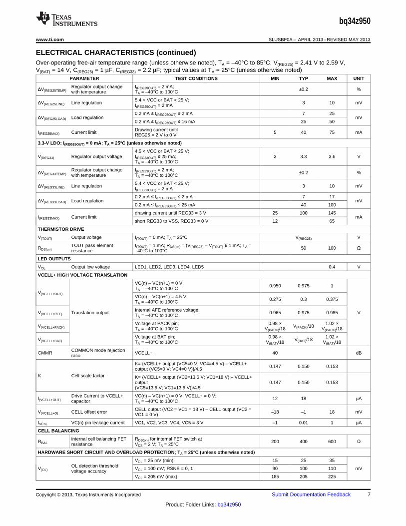
ELECTRICAL CHARACTERISTICSOver-operating free-air temperature range (unless otherwise noted), TA = –40°C to 85°C, V(REG25) = 2.41 V to 2.59 V,V(BAT) = 14 V, C(REG25) = 1 µF, C(REG33) = 2.2 µF; typical values at TA = 25°C (unless otherwise noted)
PARAMETER TEST CONDITIONS MIN TYP MAX UNIT
SUPPLY CURRENT
I(NORMAL) Firmware running 550 µA
CHG FET on; DSG FET on 124 µA
I(SLEEP) SLEEP mode CHG FET off; DSG FET on 90 µA
CHG FET off; DSG FET off 52 µA
I(SHUTDOWN) SHUTDOWN mode 0.1 1 µA
SHUTDOWN WAKE; TA = 25°C (unless otherwise noted)
Shutdown exit at VSTARTUPI(PACK) 1 µAthreshold
SRx WAKE FROM SLEEP; TA = 25°C (unless otherwise noted)
Positive or negative wakethreshold with 1.00 mV, 2.25V(WAKE) 1.25 10 mVmV, 4.5-mV and 9-mVprogrammable options
V (WAKE) = 1 mV; –0.7 0.7I(WAKE)= 0, RSNS1 = 0, RSNS0 = 1
V(WAKE) = 2.25 mV;I(WAKE) = 1, RSNS1 = 0, RSNS0 = 1; –0.8 0.8I(WAKE) = 0, RSNS1 = 1, RSNS0 = 0
V(WAKE_ACR) Accuracy of V(WAKE) mVV(WAKE) = 4.5 mV;I(WAKE) = 1, RSNS1 = 1, RSNS0 = 1; –1.0 1.0I(WAKE) = 0, RSNS1 = 1, RSNS0 = 0
V(WAKE) = 9 mV; –1.4 1.4I(WAKE) = 1, RSNS1 = 1, RSNS0 = 1
Temperature drift of V(WAKE)V(WAKE_TCO) 0.5 %/°Caccuracy
Time from application oft(WAKE) current and wake of 1 10 ms
bq34z950
WATCHDOG TIMER
Watchdog start up detecttWDTINT 250 500 1000 mstime
tWDWT Watchdog detect time 50 100 150 µs
2.5-V LDO; I(REG33OUT) = 0 mA; TA = 25°C (unless otherwise noted)
4.5 < VCC or BAT < 25 V;V(REG25) Regulator output voltage I(REG25OUT) ≤ 16 mA; 2.41 2.5 2.59 V
TA = –40°C to 100°C
6 Submit Documentation Feedback Copyright © 2013, Texas Instruments Incorporated
Product Folder Links: bq34z950
bq34z950
www.ti.com SLUSBF0A – APRIL 2013–REVISED MAY 2013
ELECTRICAL CHARACTERISTICS (continued)Over-operating free-air temperature range (unless otherwise noted), TA = –40°C to 85°C, V(REG25) = 2.41 V to 2.59 V,V(BAT) = 14 V, C(REG25) = 1 µF, C(REG33) = 2.2 µF; typical values at TA = 25°C (unless otherwise noted)
PARAMETER TEST CONDITIONS MIN TYP MAX UNIT
Regulator output change I(REG25OUT) = 2 mA;ΔV(REG25TEMP) ±0.2 %with temperature TA = –40°C to 100°C
5.4 < VCC or BAT < 25 V;ΔV(REG25LINE) Line regulation 3 10 mVI(REG25OUT) = 2 mA
0.2 mA ≤ I(REG25OUT) ≤ 2 mA 7 25ΔV(REG25LOAD) Load regulation mV
0.2 mA ≤ I(REG25OUT) ≤ 16 mA 25 50
Drawing current untilI(REG25MAX) Current limit 5 40 75 mAREG25 = 2 V to 0 V
3.3-V LDO; I(REG25OUT) = 0 mA; TA = 25°C (unless otherwise noted)
4.5 < VCC or BAT < 25 V;V(REG33) Regulator output voltage I(REG33OUT) ≤ 25 mA; 3 3.3 3.6 V
TA = –40°C to 100°C
Regulator output change I(REG33OUT) = 2 mA;ΔV(REG33TEMP) ±0.2 %with temperature TA = –40°C to 100°C
5.4 < VCC or BAT < 25 V;ΔV(REG33LINE) Line regulation 3 10 mVI(REG33OUT) = 2 mA
0.2 mA ≤ I(REG33OUT) ≤ 2 mA 7 17ΔV(REG33LOAD) Load regulation mV
0.2 mA ≤ I(REG33OUT) ≤ 25 mA 40 100
drawing current until REG33 = 3 V 25 100 145I(REG33MAX) Current limit mA
short REG33 to VSS, REG33 = 0 V 12 65
THERMISTOR DRIVE
V(TOUT) Output voltage I(TOUT) = 0 mA; TA = 25°C V(REG25) V
TOUT pass element I(TOUT) = 1 mA; RDS(on) = (V(REG25) – V(TOUT) )/ 1 mA; TA =RDS(on) 50 100 Ωresistance –40°C to 100°C
LED OUTPUTS
VOL Output low voltage LED1, LED2, LED3, LED4, LED5 0.4 V
VCELL+ HIGH VOLTAGE TRANSLATION
VC(n) – VC(n+1) = 0 V; 0.950 0.975 1TA = –40°C to 100°CV(VCELL+OUT)
VC(n) – VC(n+1) = 4.5 V; 0.275 0.3 0.375TA = –40°C to 100°C
Internal AFE reference voltage;V(VCELL+REF) Translation output 0.965 0.975 0.985 VTA = –40°C to 100°C
Voltage at PACK pin; 0.98 × 1.02 ×V(VCELL+PACK) V(PACK)/18TA = –40°C to 100°C V(PACK)/18 V(PACK)/18
Voltage at BAT pin; 0.98 × 1.02 ×V(VCELL+BAT) V(BAT)/18TA = –40°C to 100°C V(BAT)/18 V(BAT)/18
COMMON mode rejectionCMMR VCELL+ 40 dBratio
K= VCELL+ output (VC5=0 V; VC4=4.5 V) – VCELL+ 0.147 0.150 0.153output (VC5=0 V; VC4=0 V)/4.5K Cell scale factor K= VCELL+ output (VC2=13.5 V; VC1=18 V) – VCELL+
output 0.147 0.150 0.153(VC5=13.5 V; VC1=13.5 V)/4.5
Drive Current to VCELL+ VC(n) – VC(n+1) = 0 V; VCELL+ = 0 V;I(VCELL+OUT) 12 18 μAcapacitor TA = –40°C to 100°C
CELL output (VC2 = VC1 = 18 V) – CELL output (VC2 =V(VCELL+O) CELL offset error –18 –1 18 mVVC1 = 0 V)
IVCnL VC(n) pin leakage current VC1, VC2, VC3, VC4, VC5 = 3 V –1 0.01 1 μA
CELL BALANCING
internal cell balancing FET RDS(on) for internal FET switch atRBAL 200 400 600 Ωresistance VDS = 2 V; TA = 25°C
HARDWARE SHORT CIRCUIT AND OVERLOAD PROTECTION; TA = 25°C (unless otherwise noted)
VOL = 25 mV (min) 15 25 35OL detection thresholdV(OL) VOL = 100 mV; RSNS = 0, 1 90 100 110 mVvoltage accuracy
VOL = 205 mV (max) 185 205 225
Copyright © 2013, Texas Instruments Incorporated Submit Documentation Feedback 7
Product Folder Links: bq34z950

bq34z950
SLUSBF0A – APRIL 2013–REVISED MAY 2013 www.ti.com
ELECTRICAL CHARACTERISTICS (continued)Over-operating free-air temperature range (unless otherwise noted), TA = –40°C to 85°C, V(REG25) = 2.41 V to 2.59 V,V(BAT) = 14 V, C(REG25) = 1 µF, C(REG33) = 2.2 µF; typical values at TA = 25°C (unless otherwise noted)
PARAMETER TEST CONDITIONS MIN TYP MAX UNIT
V(SCC) = 50 mV (min) 30 50 70SCC detection thresholdV(SCC) V(SCC) = 200 mV; RSNS = 0, 1 180 200 220 mVvoltage accuracy
V(SCC) = 475 mV (max) 428 475 523
V(SCD) = –50 mV (min) –30 –50 –70SCD detection thresholdV(SCD) V(SCD) = –200 mV; RSNS = 0, 1 –180 –200 –220 mVvoltage accuracy
V(SCD) = –475 mV (max) –428 –475 –523
tda Delay time accuracy ±15.25 μs
Protection circuittpd 50 μspropagation delay
FET DRIVE CIRCUIT; TA = 25°C (unless otherwise noted)
V(DSGON) = V(DSG) – V(PACK);V(DSGON) DSG pin output on voltage V(GS) connected to 10 MΩ; DSG and CHG on; 8 12 16 V
TA = –40°C to 100°C
V(CHGON) = V(CHG) – V(BAT);V(CHGON) CHG pin output on voltage V(GS) = 10 MΩ; DSG and CHG on; 8 12 16 V
TA = –40°C to 100°C
V(DSGOFF) DSG pin output off voltage V(DSGOFF) = V(DSG) – V(PACK) 0.2 V
V(CHGOFF) CHG pin output off voltage V(CHGOFF) = V(CHG) – V(BAT) 0.2 V
V(CHG): V(PACK) ≥ V(PACK) + 4 V 400 1000tr Rise time CL= 4700 pF μs
V(DSG): V(BAT) ≥V(BAT) + 4V 400 1000
V(CHG): V(PACK) + V(CHGON) ≥ V(PACK)+ 40 2001 Vtf Fall time CL= 4700pF μsV(DSG): VC1 + V(DSGON) ≥ VC1 + 1 V 40 200
V(ZVCHG) ZVCHG clamp voltage BAT = 4.5 V 3.3 3.5 3.7 V
LOGIC; TA = –40°C to 100°C (unless otherwise noted)
ALERT 60 100 200R(PULLUP) Internal pullup resistance kΩ
RESET 1 3 6
ALERT 0.2Logic low output voltageVOL RESET; V(BAT) = 7 V; V(REG25) = 1.5 V; I(RESET) = 200 μA 0.4 Vlevel
GPOD; I(GPOD) = 50 μA 0.6
LOGIC SMBC, SMBD, DQ, ALERT, DISP
VIH High-level input voltage 2.0 V
VIL Low-level input voltage 0.8 V
VOH Output voltage high (1) IL = –0.5 mA VREG25–0.5 V
VOL Low-level output voltage DQ, ALERT, DISP; IL = 7 mA; 0.4 V
CI Input capacitance 5 pF
Ilkg Input leakage current 1 µA
ADC (2)
Input voltage range TS1, using Internal Vref –0.2 1 V
Conversion time 31.5 ms
Resolution (no missing 16 bitscodes)
Effective resolution 14 15 bits
Integral nonlinearity ±0.03 %FSR (3)
Offset error (4) 140 250 µV
Offset error drift (4) TA = 25°C to 85°C 2.5 18 μV/°C
Full-scale error (5) ±0.1% ±0.7%
Full-scale error drift 50 PPM/°C
(1) RC[0:7] bus(2) Unless otherwise specified, the specification limits are valid at all measurement speed modes.(3) Full-scale reference(4) Post-calibration performance and no I/O changes during conversion with SRN as the ground reference.(5) Uncalibrated performance. This gain error can be eliminated with external calibration.
8 Submit Documentation Feedback Copyright © 2013, Texas Instruments Incorporated
Product Folder Links: bq34z950

bq34z950
www.ti.com SLUSBF0A – APRIL 2013–REVISED MAY 2013
ELECTRICAL CHARACTERISTICS (continued)Over-operating free-air temperature range (unless otherwise noted), TA = –40°C to 85°C, V(REG25) = 2.41 V to 2.59 V,V(BAT) = 14 V, C(REG25) = 1 µF, C(REG33) = 2.2 µF; typical values at TA = 25°C (unless otherwise noted)
PARAMETER TEST CONDITIONS MIN TYP MAX UNIT
Effective input resistance (6) 8 MΩ
COULOMB COUNTER
Input voltage range –0.20 0.20 V
Conversion time Single conversion 250 ms
Effective resolution Single conversion 15 bits
–0.1 V to 0.20 V ±0.007 ±0.034Integral nonlinearity %FSR
–0.20 V to –0.1 V ±0.007
Offset error (7) TA = 25°C to 85°C 10 µV
Offset error drift 0.4 0.7 µV/°C
Full-scale error (8) (9) ±0.35%
Full-scale error drift 150 PPM/°C
Effective input resistance (10) TA = 25°C to 85°C 2.5 MΩ
INTERNAL TEMPERATURE SENSOR
Temperature sensorV(TEMP) –2.0 mV/°Cvoltage (11)
VOLTAGE REFERENCE
Output voltage 1.215 1.225 1.230 V
Output voltage drift 65 PPM/°C
HIGH FREQUENCY OSCILLATOR
f(OSC) Operating frequency 4.194 MHz
–3% 0.25% 3%f(EIO) Frequency error (12) (13)
TA = 20°C to 70°C –2% 0.25% 2%
t(SXO) Start-up time (14) 2.5 5 ms
LOW FREQUENCY OSCILLATOR
f(LOSC) Operating frequency 32.768 kHz
–2.5% 0.25% 2.5%f(LEIO) Frequency error (13) (15)
TA = 20°C to 70°C –1.5% 0.25% 1.5%
t(LSXO) Start-up time (14) 500 µs
(6) The A/D input is a switched-capacitor input. Since the input is switched, the effective input resistance is a measure of the averageresistance.
(7) Post-calibration performance(8) Reference voltage for the coulomb counter is typically Vref/3.969 at V(REG25) = 2.5 V, TA = 25°C.(9) Uncalibrated performance. This gain error can be eliminated with external calibration.(10) The CC input is a switched capacitor input. Since the input is switched, the effective input resistance is a measure of the average
resistance.(11) –53.7 LSB/°C(12) The frequency error is measured from 4.194 MHz.(13) The frequency drift is included and measured from the trimmed frequency at V(REG25) = 2.5 V, TA = 25°C.(14) The startup time is defined as the time it takes for the oscillator output frequency to be ±3%.(15) The frequency error is measured from 32.768 kHz.
POWER-ON RESETOver-operating free-air temperature range (unless otherwise noted), TA = –40°C to 85°C, V(REG25) = 2.41 V to 2.59 V,V(BAT) = 14 V, C(REG25) = 1 µF, C(REG33) = 2.2 µF; typical values at TA = 25°C (unless otherwise noted)
PARAMETER TEST CONDITIONS MIN TYP MAX UNIT
VIT– Negative-going voltage input 1.7 1.8 1.9 V
VHYS Power-on reset hysteresis 5 125 200 mV
Active low time after power up or watchdogtRST RESET active low time 100 250 560 µsreset
Copyright © 2013, Texas Instruments Incorporated Submit Documentation Feedback 9
Product Folder Links: bq34z950

1.76
1.77
1.78
1.79
1.8
1.81
-40 -20 0 20 40 60 80
T - Free-Air Temperature - °CA
Po
we
r-O
n R
es
et
Ne
ga
tiv
e-G
oin
g V
olt
ag
e -
V
POWER ON RESET BEHAVIOR
FREE-AIR TEMPERATURE
VS
bq34z950
SLUSBF0A – APRIL 2013–REVISED MAY 2013 www.ti.com
DATA FLASH CHARACTERISTICS OVER RECOMMENDED OPERATING TEMPERATURE ANDSUPPLY VOLTAGETypical values at TA = 25°C and V(REG25) = 2.5 V (unless otherwise noted)
PARAMETER TEST CONDITIONS MIN TYP MAX UNIT
Data retention 10 Years
Flash programming write-cycles 20k Cycles
t(ROWPROG) Row programming time See (1) 2 ms
t(MASSERASE) Mass-erase time 200 ms
t(PAGEERASE) Page-erase time 20 ms
I(DDPROG) Flash-write supply current 5 10 mA
I(DDERASE) Flash-erase supply current 5 10 mA
RAM/REGISTER BACKUP
V(RBI) > V(RBI)MIN , VREG25 < VIT–, TA = 85°C 1000 2500I(RB) RB data-retention input current nA
V(RBI) > V(RBI)MIN , VREG25 < VIT–, TA = 25°C 90 220
V(RB) RB data-retention input voltage (1) 1.7 V
(1) Specified by design. Not production tested.
SMBus TIMING CHARACTERISTICSTA = –40°C to 85°C Typical Values at TA = 25°C and VREG25 = 2.5 V (Unless Otherwise Noted)
PARAMETER TEST CONDITIONS MIN TYP MAX UNIT
f(SMB) SMBus operating frequency SLAVE mode, SMBC 50% duty cycle 10 100 kHz
f(MAS) SMBus master clock frequency MASTER mode, No clock low slave 51.2 kHzextend
Bus free time between start and stopt(BUF) 4.7 µs(see Figure 1)
t(HD:STA) Hold time after (repeated) start (see Figure 1) 4 µs
t(SU:STA) Repeated start setup time (see Figure 1) 4.7 µs
t(SU:STO) Stop setup time (see Figure 1) 4 µs
t(HD:DAT) RECEIVE mode 0 nsData hold time (see Figure 1)
TRANSMIT mode 300
10 Submit Documentation Feedback Copyright © 2013, Texas Instruments Incorporated
Product Folder Links: bq34z950

SMBC
SMBD
SMBC
SMBD
SMBC
SMBD
S
tSU(STA)
SP
tBUFtSU(STO)
tR tF
SMBC
SMBD
tTIMEOUT
tHIGH
tLOW
tF tR
tHD(DAT) tSU(DAT)
tHD(STA)
Start and Stop condition Wait and Hold condition
Timeout condition Repeated Start condition
bq34z950
www.ti.com SLUSBF0A – APRIL 2013–REVISED MAY 2013
SMBus TIMING CHARACTERISTICS (continued)TA = –40°C to 85°C Typical Values at TA = 25°C and VREG25 = 2.5 V (Unless Otherwise Noted)
PARAMETER TEST CONDITIONS MIN TYP MAX UNIT
t(SU:DAT) Data setup time (see Figure 1) 250 ns
t(TIMEOUT) Error signal/detect (see Figure 1) See (1) 25 35 µs
t(LOW) Clock low period (see Figure 1) 4.7 µs
t(HIGH) Clock high period (see Figure 1) See (2) 4 50 µs
t(LOW:SEXT) Cumulative clock low slave extend time See (3) 25 ms
Cumulative clock low master extend timet(LOW:MEXT) See (4) 10 ms(see Figure 1)
tf Clock/data fall time See (5) 300 ns
tr Clock/data rise time See (6) 1000 ns
(1) The bq34z950 times out when any clock low exceeds t(TIMEOUT).(2) t(HIGH), Max, is the minimum bus idle time. SMBC = SMBD = 1 for t > 50 ms causes reset of any transaction involving bq34z950 that is
in progress. This specification is valid when the NC_SMB control bit remains in the default cleared state (CLK[0]=0).(3) t(LOW:SEXT) is the cumulative time a slave device is allowed to extend the clock cycles in one message from initial start to the stop.(4) t(LOW:MEXT) is the cumulative time a master device is allowed to extend the clock cycles in one message from initial start to the stop.(5) Rise time tr = VILMAX – 0.15) to (VIHMIN + 0.15)(6) Fall time tf = 0.9VDD to (VILMAX – 0.15)
A. SCLKACK is the acknowledge-related clock pulse generated by the master.
Figure 1. SMBus Timing Diagram
Copyright © 2013, Texas Instruments Incorporated Submit Documentation Feedback 11
Product Folder Links: bq34z950

DQ(R/W 1)
DQ(R/W 0)
DQ(BREAK)
t(STRH)
t(STRB)
t(DSU)
t(SSU)
t(CYCH), t , t(CYCB) (B)
t(DH)
t(SH)
t(DV)
t(BR)
t(SV)
T0269-01
bq34z950
SLUSBF0A – APRIL 2013–REVISED MAY 2013 www.ti.com
DQ 1-WIRE INTERFACE
DQ TIMING SPECIFICATIONSVDD = 2.4 V to 2.6 V, TA = –40°C to 85°C (unless otherwise noted)
PARAMETER TEST CONDITIONS MIN TYP MAX UNIT
t(CYCH) Cycle time, host to bq34z950 See (1) 3 ms
t(CYCB) Cycle time, bq34z950 to host 3 6 ms
t(STRH) Start hold, host to bq34z950 5 ns
t(STRB) Start hold, bq34z950 to host 500 750 μs
t(DSU) Data setup μs
t(DH) Data hold 750 μs
t(DV) Data valid 1.5 ms
t(SSU) Stop setup 2.25 ms
t(SH) Stop hold 700 μs
t(SV) Stop valid 2.95 ms
t(B) Break 3 ms
t(BR) Break recovery 1 ms
(1) The open-drain DQ pin should be pulled to at least VCC by the host system for proper DQ operation. DQ may be left floating if the serialinterface is not used.
Figure 2. DQ Timing Diagram
DQ timing for this device is selectable by adjusting values in Data Flash Sub Class 0x113. See Figure 3 for anoverview of the flash values.
12 Submit Documentation Feedback Copyright © 2013, Texas Instruments Incorporated
Product Folder Links: bq34z950

Data 7Write 1Bit 7 of Address
Data 6Write 0
Data 4Data 5 Data 3 Data 2 Data 1 Data 0
Sla
veR
sp_
De
lay
Wr1
_Lo
Wr0
_Lo
Wr_
0_
to_
1_D
ela
y
Wr_
0_
to_
1_
Dela
y
Wr1
_R
C
Wr0
_R
C
ParameterTime
( s)m
TimeCounts
BR_LO
BR_RC
Wr0_Lo
Wr0_RC
Wr1_Lo
Wr1_RC
Rd0_Lo
Rd1_Lo
RD_TO
RD_RS
Wr_0_to_1_Delay
SlaveRsp_Delay
2699
1000
1775
1225
549
2451
1149
1100
0
299
99
3020
2830
1048
1861
1284
576
2570
1205
1153
0
314
104
3166
T0270-01
bq34z950
www.ti.com SLUSBF0A – APRIL 2013–REVISED MAY 2013
Figure 3. DQ Timing Control
Copyright © 2013, Texas Instruments Incorporated Submit Documentation Feedback 13
Product Folder Links: bq34z950

bq34z950
SLUSBF0A – APRIL 2013–REVISED MAY 2013 www.ti.com
FEATURE SET
Primary (First-Level) Safety Features
The bq34z950 supports a wide range of battery and system protection features that can easily be configured.The primary safety features include:
• Cell over/undervoltage protection• Charge and discharge overcurrent• Short circuit• Charge and discharge overtemperature• AFE watchdog
Secondary (Second-Level) Safety Features
The secondary safety features of the bq34z950 can be used to indicate more serious faults. The secondarysafety protection features include:
• Safety overvoltage• Safety overcurrent in charge and discharge• Safety overtemperature in Charge and Discharge• Charge FET and 0-V charge FET fault• Discharge FET fault• AFE communication fault
Charge Control Features
The bq34z950 charge control features include:
• Reports the appropriate charging current needed for constant current charging, and the appropriate chargingvoltage needed for constant voltage charging to a smart charger using SMBus broadcasts.
• Determines the chemical state of charge of each battery cell using Impedance Track technology, and canreduce the charge difference of the battery cells in a fully charged state of the battery pack, gradually usingthe cell balancing algorithm during charging. This prevents fully charged cells from overcharging and causingexcessive degradation, and also increases the usable pack energy by preventing premature chargetermination.
• Supports precharging/zero-volt charging• Supports fast charging• Supports charge inhibit and charge suspend if the battery pack temperature is out of temperature range• Reports charging fault and also indicates charge status via charge and discharge alarms
Gas Gauging
The bq34z950 uses Impedance Track technology to measure and calculate the available charge in battery cells.The achievable accuracy is better than 1% error over the lifetime of the battery, and there is no full chargedischarge learning cycle required.
See the Theory and Implementation of Impedance Track Battery Fuel-Gauging Algorithm application note(SLUA364) for further details.
Authentication
The bq34z950 supports authentication by the host using SHA-1.
Power Modes
The bq34z950 supports three power modes to reduce power consumption:
• In NORMAL mode, the bq34z950 performs measurements, calculations, protection decisions, and dataupdates in 1-s intervals. Between these intervals, the bq34z950 is in a reduced power state.
14 Submit Documentation Feedback Copyright © 2013, Texas Instruments Incorporated
Product Folder Links: bq34z950

bq34z950
www.ti.com SLUSBF0A – APRIL 2013–REVISED MAY 2013
• In SLEEP mode, the bq34z950 performs measurements, calculations, protection decisions, and data updatesin adjustable time intervals. Between these intervals, the bq34z950 is in a reduced power state. Thebq34z950 has a wake function that enables exit from SLEEP mode when current flow or failure is detected.
• In SHUTDOWN mode, the bq34z950 is completely disabled.
CONFIGURATION
Oscillator Function
The bq34z950 fully integrates the system oscillators. Therefore, the bq34z950 requires no external componentsfor this feature.
BATTERY PARAMETER MEASUREMENTS
The bq34z950 uses an integrating delta-sigma analog-to-digital converter (ADC) for current measurement, and asecond delta-sigma ADC for individual cell and battery voltage and temperature measurement.
Charge and Discharge Counting
The integrating delta-sigma ADC measures the charge/discharge flow of the battery by measuring the voltagedrop across a small-value sense resistor between the SRP and SRN pins. The integrating ADC measures bipolarsignals from –0.25 V to 0.25 V. The bq34z950 detects charge activity when VSR = V(SRP) – V(SRN) is positive, anddischarge activity when VSR = V(SRP) – V(SRN) is negative. The bq34z950 continuously integrates the signal overtime, using an internal counter. The fundamental rate of the counter is 0.65 nV/h.
Voltage
The bq34z950 updates the individual series cell voltages at 1-s intervals. The internal ADC of the bq34z950measures the voltage, and scales and calibrates it appropriately. This data is also used to calculate theimpedance of the cell for the Impedance Track gas gauging.
Current
The bq34z950 uses the GSRP and GSRN inputs to measure and calculate the battery charge and dischargecurrent using a 5-mΩ to 20-mΩ typical sense resistor.
Auto Calibration
The bq34z950 provides an autocalibration feature to cancel the voltage offset error across SRP and SRN formaximum charge measurement accuracy. The bq34z950 performs autocalibration when the SMBus and DQlines stay low for a minimum of 16 s, and the DF:AutoCal_PerSleep counter has counted up to its programmedvalue. The AutoCal_PerSleep counter provides a way for the user to specify the number of times the part canenter SLEEP mode before an offset calibration is performed. This is to prohibit unnecessary calibration cycles forbattery packs that enter SLEEP mode frequently. The bq34z950 is capable of automatic offset calibration downto 1 μV.
Temperature
The bq34z950 has an internal temperature sensor and external temperature sensor input, TS1, which can beused to sense the environmental temperature of the batteries. The bq34z950 can be configured to use internal orexternal temperature sensors. The external sensor input is used in conjunction with an NTC thermistor (default isSemitec 103AT).
COMMUNICATIONS
The bq34z950 uses SMBus v1.1 with MASTER mode and package error checking (PEC) options per the SBSspecification. Integrated error checking is not available on the DQ interface.
SMBus/DQ On and Off States
The bq34z950 detects an SMBus/DQ off state when SMBC, SMBD, and DQ are logic-low for ≥ 2 seconds.Clearing this state requires either SMBC or SMBD or DQ to transition high. Within 1 ms, the communication busis available.
Copyright © 2013, Texas Instruments Incorporated Submit Documentation Feedback 15
Product Folder Links: bq34z950

bq34z950
SLUSBF0A – APRIL 2013–REVISED MAY 2013 www.ti.com
SHA-1 Over DQ
SHA-1 Overview
The host sends a randomly generated 20-byte challenge, and then reads the 20-byte response generated by thebq34z950. The response generated by the bq34z950 is calculated using the SHA-1 hash algorithm and a sharedprivate key known by both parties to the transaction. The host compares the bq34z950 response to the expectedresponse, and if they agree, then the host concludes that the bq34z950 knows the key, and is thusauthenticated.
The 20-byte challenge/response is written/read using registers 0x1B–0x2E. The bq34z950 calculates theresponse when a write of any data value is issued to register 0x2F. DQ communication is ignored when theresponse is calculated, which takes approximately 22 ms.
SHA-1 Usage Procedure
Use the following two steps to implement the SHA-1 algorithm in the bq34z950:1. Create a unique authentication key and write it to the part during assembly.
The authentication key resides in the SMBus addresses 0x63–0x66 in 4-byte strings. The four strings areread/write accessible until the bq34z950 is sealed. When written using an SMBus string write command, theyare retained permanently in flash memory and can only be changed when the bq34z950 is unsealed. Theyare stored in Little Endian format. The SHA-1 authentication key defaults to0123456789abcdeffedcba9876543210 in the bq34z950. This is a default and is not intended for production.It should be changed to a unique key prior to production to ensure that security is not compromised.
For more details, see Using SHA-1 in bq20Zxx Family of Gas Gauges (SLUA359).
The host sends a 20-byte random challenge string. This string must be written to the bq34z950 DQ registersin Little Endian format.
Little Endian representation is as follows:Byte00, Byte01, Byte02, Byte03, Byte04, Byte05, Byte06, Byte07, Byte08, Byte09,Byte0A, Byte0B, Byte0C, Byte0D, Byte0E, Byte0F, Byte10, Byte11, Byte12, Byte13
Big Endian representation is as follows:Byte13, Byte12, Byte11, Byte10, Byte0F, Byte0E, Byte0D, Byte0C, Byte0B, Byte0A,Byte09, Byte08, Byte07, Byte06, Byte05, Byte04, Byte10, Byte03, Byte02, Byte01, Byte00
2. Implement SHA-1 in the OEM host system.(a) The host must know the SHA-1 key defined in Step 1. This key is used in the host system to determine
what the response should be.(b) The host must issue a random challenge: The host sends a challenge using a 20-byte string write to the
SMBus command 0x2F or to the DQ registers in Little Endian format. For SHA-1 over DQ bus, the writeof 20 bytes must be followed by a write access to register 0x2F to start the authentication. Any value canbe written. It is important that the challenge be random every time to ensure security.
(c) The host computes the response: With the known SHA-1 authentication key and random challenge, thehost computes the anticipated response from the bq34z950.
(d) bq34z950 computes the response: The bq34z950 computes the response at the same time that the hostis computing it. The bq34z950 should be given greater than 22 ms to compute the response and put itinto memory or the DQ registers for retrieval.
(e) The host must read the response: The host reads the response from the same DQ registers to which thechallenge was written. The response is a 20-byte string read in Little Endian format.
(f) The host must validate the response: The host must compare the response read from the bq34z950 towhat was computed in Step 2.c above.
(g) If the response is validated, then the battery is authenticated. Otherwise, the host can reject the pack.
16 Submit Documentation Feedback Copyright © 2013, Texas Instruments Incorporated
Product Folder Links: bq34z950
bq34z950
www.ti.com SLUSBF0A – APRIL 2013–REVISED MAY 2013
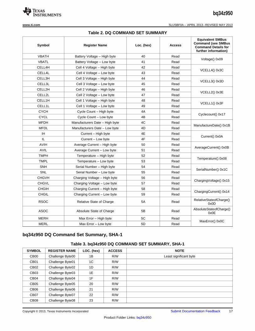
Table 2. DQ COMMAND SET SUMMARY
Equivalent SMBusCommand (see SMBusSymbol Register Name Loc. (hex) Access Command Details for
further information)
VBATH Battery Voltage – High byte 40 ReadVoltage() 0x09
VBATL Battery Voltage – Low byte 41 Read
CELL4H Cell 4 Voltage – High byte 42 ReadVCELL4() 0x3C
CELL4L Cell 4 Voltage – Low byte 43 Read
CELL3H Cell 3 Voltage – High byte 44 ReadVCELL3() 0x3D
CELL3L Cell 3 Voltage – Low byte 45 Read
CELL2H Cell 2 Voltage – High byte 46 ReadVCELL2() 0x3E
CELL2L Cell 2 Voltage – Low byte 47 Read
CELL1H Cell 1 Voltage – High byte 48 ReadVCELL1() 0x3F
CELL1L Cell 1 Voltage – Low byte 49 Read
CYCH Cycle Count – High byte 4A ReadCyclecount() 0x17
CYCL Cycle Count – Low byte 4B Read
MFDH Manufacturers Date – High byte 4C ReadManufactureDate() 0x1B
MFDL Manufacturers Date – Low byte 4D Read
IH Current – High byte 4E ReadCurrent() 0x0A
IL Current – Low byte 4F Read
AVIH Average Current – High byte 50 ReadAverageCurrent() 0x0B
AVIL Average Current – Low byte 51 Read
TMPH Temperature – High byte 52 ReadTemperature() 0x08
TMPL Temperature – Low byte 53 Read
SNH Serial Number – High byte 54 ReadSerialNumber() 0x1C
SNL Serial Number – Low byte 55 Read
CHGVH Charging Voltage – High byte 56 ReadChargingVoltage() 0x15
CHGVL Charging Voltage – Low byte 57 Read
CHGIH Charging Current – High byte 58 ReadChargingCurrent() 0x14
CHGIL Charging Current – Low byte 59 Read
RelativeStateofCharge()RSOC Relative State of Charge 5A Read 0x0D
AbsoluteStateofCharge()ASOC Absolute State of Charge 5B Read 0x0E
MERH Max Error – High byte 5C ReadMaxError() 0x0C
MERL Max Error – Low byte 5D Read
bq34z950 DQ Command Set Summary, SHA-1
Table 3. bq34z950 DQ COMMAND SET SUMMARY, SHA-1
SYMBOL REGISTER NAME LOC. (hex) ACCESS NOTE
CB00 Challenge Byte00 1B R/W Least significant byte
CB01 Challenge Byte01 1C R/W
CB02 Challenge Byte02 1D R/W
CB03 Challenge Byte03 1E R/W
CB04 Challenge Byte04 1F R/W
CB05 Challenge Byte05 20 R/W
CB06 Challenge Byte06 21 R/W
CB07 Challenge Byte07 22 R/W
CB08 Challenge Byte08 23 R/W
Copyright © 2013, Texas Instruments Incorporated Submit Documentation Feedback 17
Product Folder Links: bq34z950

bq34z950
SLUSBF0A – APRIL 2013–REVISED MAY 2013 www.ti.com
Table 3. bq34z950 DQ COMMAND SET SUMMARY, SHA-1 (continued)
SYMBOL REGISTER NAME LOC. (hex) ACCESS NOTE
CB09 Challenge Byte09 24 R/W
CB0A Challenge Byte0A 25 R/W
CB0B Challenge Byte0B 26 R/W
CB0C Challenge Byte0C 27 R/W
CB0D Challenge Byte0D 28 R/W
CB0E Challenge Byte0E 29 R/W
CB0F Challenge Byte0F 2A R/W
CB10 Challenge Byte10 2B R/W
CB11 Challenge Byte11 2C R/W
CB12 Challenge Byte12 2D R/W
CB13 Challenge Byte13 2E R/W Most significant byte
AUTHST Start Authentication 2F Write A write of any value starts the authentication algorithm
18 Submit Documentation Feedback Copyright © 2013, Texas Instruments Incorporated
Product Folder Links: bq34z950

bq34z950
www.ti.com SLUSBF0A – APRIL 2013–REVISED MAY 2013
SBS Standard Commands
Table 4. SBS STANDARD COMMANDS
SBS Size in Min Max DefaultMode Name Format UnitCmd Bytes Value Value Value
0x00 R/W ManufacturerAccess Hex 2 0x0000 0xffff —
0x01 R/W RemainingCapacityAlarm Unsigned int 2 0 65,535 — mAh or10 mWh
0x02 R/W RemainingTimeAlarm Unsigned int 2 0 65,535 — min
0x03 R/W BatteryMode Hex 2 0x0000 0xffff —
0x04 R/W AtRate Signed int 2 –32,768 32,767 — mA or 10mW
0x05 R AtRateTimeToFull Unsigned int 2 0 65,535 — min
0x06 R AtRateTimeToEmpty Unsigned int 2 0 65,535 — min
0x07 R AtRateOK Unsigned int 2 0 65,535 —
0x08 R Temperature Unsigned int 2 0 65,535 — 0.1°K
0x09 R Voltage Unsigned int 2 0 20,000 — mV
0x0A R Current Signed int 2 –32,768 32,767 — mA
0x0B R AverageCurrent Signed int 2 –32,768 32,767 — mA
0x0C R MaxError Unsigned int 1 0 100 — %
0x0D R RelativeStateOfCharge Unsigned int 1 0 100 — %
0x0E R AbsoluteStateOfCharge Unsigned int 1 0 100 — %
0x0F R/W RemainingCapacity Unsigned int 2 0 65,535 — mAh or10 mWh
0x10 R FullChargeCapacity Unsigned int 2 0 65,535 — mAh or10 mWh
0x11 R RunTimeToEmpty Unsigned int 2 0 65,535 — min
0x12 R AverageTimeToEmpty Unsigned int 2 0 65,535 — min
0x13 R AverageTimeToFull Unsigned int 2 0 65,535 — min
0x14 R ChargingCurrent Unsigned int 2 0 65,535 — mA
0x15 R ChargingVoltage Unsigned int 2 0 65,535 — mV
0x16 R BatteryStatus Unsigned int 2 0x0000 0xffff —
0x17 R/W CycleCount Unsigned int 2 0 65,535 —
0x18 R/W DesignCapacity Unsigned int 2 0 65,535 — mAh or10 mWh
0x19 R/W DesignVoltage Unsigned int 2 7,000 16,000 14,400 mV
0x1A R/W SpecificationInfo Unsigned int 2 0x0000 0xffff 0x0031
0x1B R/W ManufactureDate Unsigned int 2 0 65,535 0
0x1C R/W SerialNumber Hex 2 0x0000 0xffff —
0x20 R/W ManufacturerName String 11 + 1 — — Texas ASCIIInstruments
0x21 R/W DeviceName String 7 + 1 — — bq34z950 ASCII
0x22 R/W DeviceChemistry String 4 + 1 — — LION ASCII
0x23 R ManufacturerData String 14 + 1 — — — ASCII
0x2F R/W Authenticate String 20 + 1 — — — ASCII
0x3C R CellVoltage4 Unsigned int 2 0 65,535 — mV
0x3D R CellVoltage3 Unsigned int 2 0 65,535 — mV
0x3E R CellVoltage2 Unsigned int 2 0 65,535 — mV
0x3F R CellVoltage1 Unsigned int 2 0 65,535 — mV
Copyright © 2013, Texas Instruments Incorporated Submit Documentation Feedback 19
Product Folder Links: bq34z950

bq34z950
SLUSBF0A – APRIL 2013–REVISED MAY 2013 www.ti.com
Table 5. EXTENDED SBS COMMANDS
SBS Size in DefaultMode Name Format Min Value Max Value UnitCmd Bytes Value
0x45 R AFEData String 11 + 1 — — — ASCII
0x46 R/W FETControl Hex 1 0x00 0xff —
0x4F R StateOfHealth Unsigned int 1 0 100 — %
0x51 R SafetyStatus Hex 2 0x0000 0xffff —
0x53 R PFStatus Hex 2 0x0000 0xffff —
0x54 R OperationStatus Hex 2 0x0000 0xffff —
0x55 R ChargingStatus Hex 2 0x0000 0xffff —
0x57 R ResetData Hex 2 0x0000 0xffff —
0x5A R PackVoltage Unsigned int 2 0 65,535 — mV
0x5D R AverageVoltage Unsigned int 2 0 65,535 — mV
0x60 R/W UnSealKey Hex 4 0x0000 0000 0xffff ffff —
0x61 R/W FullAccessKey Hex 4 0x0000 0000 0xffff ffff —
0x62 R/W PFKey Hex 4 0x0000 0000 0xffff ffff —
0x63 R/W AuthenKey3 Hex 4 0x0000 0000 0xffff ffff —
0x64 R/W AuthenKey2 Hex 4 0x0000 0000 0xffff ffff —
0x65 R/W AuthenKey1 Hex 4 0x0000 0000 0xffff ffff —
0x66 R/W AuthenKey0 Hex 4 0x0000 0000 0xffff ffff —
0x70 R/W ManufacturerInfo String 8 + 1 — — —
0x71 R/W SenseResistor Unsigned int 2 0 65,535 — μΩ0x77 R/W DataFlashSubClassID Hex 2 0x0000 0xffff —
0x78 R/W DataFlashSubClassPage1 Hex 32 — — —
0x79 R/W DataFlashSubClassPage2 Hex 32 — — —
0x7A R/W DataFlashSubClassPage3 Hex 32 — — —
0x7B R/W DataFlashSubClassPage4 Hex 32 — — —
0x7C R/W DataFlashSubClassPage5 Hex 32 — — —
0x7D R/W DataFlashSubClassPage6 Hex 32 — — —
0x7E R/W DataFlashSubClassPage7 Hex 32 — — —
0x7F R/W DataFlashSubClassPage8 Hex 32 — — —
20 Submit Documentation Feedback Copyright © 2013, Texas Instruments Incorporated
Product Folder Links: bq34z950
bq34z950
www.ti.com SLUSBF0A – APRIL 2013–REVISED MAY 2013
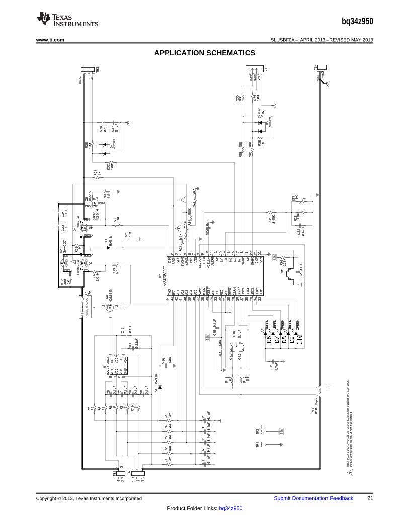
APPLICATION SCHEMATICS
Copyright © 2013, Texas Instruments Incorporated Submit Documentation Feedback 21
Product Folder Links: bq34z950
bq34z950
SLUSBF0A – APRIL 2013–REVISED MAY 2013 www.ti.com
22 Submit Documentation Feedback Copyright © 2013, Texas Instruments Incorporated
Product Folder Links: bq34z950

bq34z950
www.ti.com SLUSBF0A – APRIL 2013–REVISED MAY 2013
REVISION HISTORY
Changes from Original (April 2013) to Revision A Page
• Deleted Lifetime Data Logging from Features list ................................................................................................................ 1
Copyright © 2013, Texas Instruments Incorporated Submit Documentation Feedback 23
Product Folder Links: bq34z950

PACKAGE OPTION ADDENDUM
www.ti.com 21-May-2013
Addendum-Page 1
PACKAGING INFORMATION
Orderable Device Status(1)
Package Type PackageDrawing
Pins PackageQty
Eco Plan(2)
Lead/Ball Finish MSL Peak Temp(3)
Op Temp (°C) Device Marking(4/5)
Samples
BQ34Z950DBT ACTIVE TSSOP DBT 44 40 Green (RoHS& no Sb/Br)
CU NIPDAU Level-2-260C-1 YEAR -40 to 85 BQ34Z950
BQ34Z950DBTR ACTIVE TSSOP DBT 44 2000 Green (RoHS& no Sb/Br)
CU NIPDAU Level-2-260C-1 YEAR -40 to 85 BQ34Z950
(1) The marketing status values are defined as follows:ACTIVE: Product device recommended for new designs.LIFEBUY: TI has announced that the device will be discontinued, and a lifetime-buy period is in effect.NRND: Not recommended for new designs. Device is in production to support existing customers, but TI does not recommend using this part in a new design.PREVIEW: Device has been announced but is not in production. Samples may or may not be available.OBSOLETE: TI has discontinued the production of the device.
(2) Eco Plan - The planned eco-friendly classification: Pb-Free (RoHS), Pb-Free (RoHS Exempt), or Green (RoHS & no Sb/Br) - please check http://www.ti.com/productcontent for the latest availabilityinformation and additional product content details.TBD: The Pb-Free/Green conversion plan has not been defined.Pb-Free (RoHS): TI's terms "Lead-Free" or "Pb-Free" mean semiconductor products that are compatible with the current RoHS requirements for all 6 substances, including the requirement thatlead not exceed 0.1% by weight in homogeneous materials. Where designed to be soldered at high temperatures, TI Pb-Free products are suitable for use in specified lead-free processes.Pb-Free (RoHS Exempt): This component has a RoHS exemption for either 1) lead-based flip-chip solder bumps used between the die and package, or 2) lead-based die adhesive used betweenthe die and leadframe. The component is otherwise considered Pb-Free (RoHS compatible) as defined above.Green (RoHS & no Sb/Br): TI defines "Green" to mean Pb-Free (RoHS compatible), and free of Bromine (Br) and Antimony (Sb) based flame retardants (Br or Sb do not exceed 0.1% by weightin homogeneous material)
(3) MSL, Peak Temp. -- The Moisture Sensitivity Level rating according to the JEDEC industry standard classifications, and peak solder temperature.
(4) There may be additional marking, which relates to the logo, the lot trace code information, or the environmental category on the device.
(5) Multiple Device Markings will be inside parentheses. Only one Device Marking contained in parentheses and separated by a "~" will appear on a device. If a line is indented then it is a continuationof the previous line and the two combined represent the entire Device Marking for that device.
Important Information and Disclaimer:The information provided on this page represents TI's knowledge and belief as of the date that it is provided. TI bases its knowledge and belief on informationprovided by third parties, and makes no representation or warranty as to the accuracy of such information. Efforts are underway to better integrate information from third parties. TI has taken andcontinues to take reasonable steps to provide representative and accurate information but may not have conducted destructive testing or chemical analysis on incoming materials and chemicals.TI and TI suppliers consider certain information to be proprietary, and thus CAS numbers and other limited information may not be available for release.
In no event shall TI's liability arising out of such information exceed the total purchase price of the TI part(s) at issue in this document sold by TI to Customer on an annual basis.
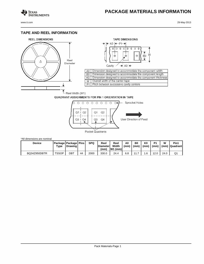
TAPE AND REEL INFORMATION
*All dimensions are nominal
Device PackageType
PackageDrawing
Pins SPQ ReelDiameter
(mm)
ReelWidth
W1 (mm)
A0(mm)
B0(mm)
K0(mm)
P1(mm)
W(mm)
Pin1Quadrant
BQ34Z950DBTR TSSOP DBT 44 2000 330.0 24.4 6.8 11.7 1.6 12.0 24.0 Q1
PACKAGE MATERIALS INFORMATION
www.ti.com 29-May-2013
Pack Materials-Page 1

*All dimensions are nominal
Device Package Type Package Drawing Pins SPQ Length (mm) Width (mm) Height (mm)
BQ34Z950DBTR TSSOP DBT 44 2000 367.0 367.0 45.0
PACKAGE MATERIALS INFORMATION
www.ti.com 29-May-2013
Pack Materials-Page 2

www.ti.com
PACKAGE OUTLINE
C
42X 0.5
2X10.5
44X 0.270.17
TYP6.66.2
1.2 MAX
0.150.05
0.25GAGE PLANE
-80
BNOTE 4
4.54.3
A
NOTE 3
11.110.9
0.750.50
(0.15) TYP
TSSOP - 1.2 mm max heightDBT0044ASMALL OUTLINE PACKAGE
4220223/A 02/2017
1
2223
44
0.08 C A B
PIN 1 INDEXAREA
SEE DETAIL A
0.1 C
NOTES: 1. All linear dimensions are in millimeters. Any dimensions in parenthesis are for reference only. Dimensioning and tolerancing per ASME Y14.5M. 2. This drawing is subject to change without notice. 3. This dimension does not include mold flash, protrusions, or gate burrs. Mold flash, protrusions, or gate burrs shall not exceed 0.15 mm per side. 4. This dimension does not include interlead flash. Interlead flash shall not exceed 0.25 mm per side.
SEATINGPLANE
A 20DETAIL ATYPICAL
SCALE 1.500

www.ti.com
EXAMPLE BOARD LAYOUT
0.05 MAXALL AROUND
0.05 MINALL AROUND
44X (1.5)
44X (0.3)
42X (0.5)
(5.8)
(R0.05) TYP
TSSOP - 1.2 mm max heightDBT0044ASMALL OUTLINE PACKAGE
4220223/A 02/2017
NOTES: (continued) 5. Publication IPC-7351 may have alternate designs. 6. Solder mask tolerances between and around signal pads can vary based on board fabrication site.
LAND PATTERN EXAMPLEEXPOSED METAL SHOWN
SCALE: 8X
SYMM
SYMM
1
22 23
44
15.000
METALSOLDER MASKOPENING
METAL UNDERSOLDER MASK
SOLDER MASKOPENING
EXPOSED METALEXPOSED METAL
SOLDER MASK DETAILS
NON-SOLDER MASKDEFINED
(PREFERRED)
SOLDER MASKDEFINED

www.ti.com
EXAMPLE STENCIL DESIGN
44X (1.5)
44X (0.3)
42X (0.5)
(5.8)
(R0.05) TYP
TSSOP - 1.2 mm max heightDBT0044ASMALL OUTLINE PACKAGE
4220223/A 02/2017
NOTES: (continued) 7. Laser cutting apertures with trapezoidal walls and rounded corners may offer better paste release. IPC-7525 may have alternate design recommendations. 8. Board assembly site may have different recommendations for stencil design.
SOLDER PASTE EXAMPLEBASED ON 0.125 mm THICK STENCIL
SCALE: 8X
SYMM
SYMM
1
22 23
44
IMPORTANT NOTICE
Texas Instruments Incorporated (TI) reserves the right to make corrections, enhancements, improvements and other changes to itssemiconductor products and services per JESD46, latest issue, and to discontinue any product or service per JESD48, latest issue. Buyersshould obtain the latest relevant information before placing orders and should verify that such information is current and complete.TI’s published terms of sale for semiconductor products (http://www.ti.com/sc/docs/stdterms.htm) apply to the sale of packaged integratedcircuit products that TI has qualified and released to market. Additional terms may apply to the use or sale of other types of TI products andservices.Reproduction of significant portions of TI information in TI data sheets is permissible only if reproduction is without alteration and isaccompanied by all associated warranties, conditions, limitations, and notices. TI is not responsible or liable for such reproduceddocumentation. Information of third parties may be subject to additional restrictions. Resale of TI products or services with statementsdifferent from or beyond the parameters stated by TI for that product or service voids all express and any implied warranties for theassociated TI product or service and is an unfair and deceptive business practice. TI is not responsible or liable for any such statements.Buyers and others who are developing systems that incorporate TI products (collectively, “Designers”) understand and agree that Designersremain responsible for using their independent analysis, evaluation and judgment in designing their applications and that Designers havefull and exclusive responsibility to assure the safety of Designers' applications and compliance of their applications (and of all TI productsused in or for Designers’ applications) with all applicable regulations, laws and other applicable requirements. Designer represents that, withrespect to their applications, Designer has all the necessary expertise to create and implement safeguards that (1) anticipate dangerousconsequences of failures, (2) monitor failures and their consequences, and (3) lessen the likelihood of failures that might cause harm andtake appropriate actions. Designer agrees that prior to using or distributing any applications that include TI products, Designer willthoroughly test such applications and the functionality of such TI products as used in such applications.TI’s provision of technical, application or other design advice, quality characterization, reliability data or other services or information,including, but not limited to, reference designs and materials relating to evaluation modules, (collectively, “TI Resources”) are intended toassist designers who are developing applications that incorporate TI products; by downloading, accessing or using TI Resources in anyway, Designer (individually or, if Designer is acting on behalf of a company, Designer’s company) agrees to use any particular TI Resourcesolely for this purpose and subject to the terms of this Notice.TI’s provision of TI Resources does not expand or otherwise alter TI’s applicable published warranties or warranty disclaimers for TIproducts, and no additional obligations or liabilities arise from TI providing such TI Resources. TI reserves the right to make corrections,enhancements, improvements and other changes to its TI Resources. TI has not conducted any testing other than that specificallydescribed in the published documentation for a particular TI Resource.Designer is authorized to use, copy and modify any individual TI Resource only in connection with the development of applications thatinclude the TI product(s) identified in such TI Resource. NO OTHER LICENSE, EXPRESS OR IMPLIED, BY ESTOPPEL OR OTHERWISETO ANY OTHER TI INTELLECTUAL PROPERTY RIGHT, AND NO LICENSE TO ANY TECHNOLOGY OR INTELLECTUAL PROPERTYRIGHT OF TI OR ANY THIRD PARTY IS GRANTED HEREIN, including but not limited to any patent right, copyright, mask work right, orother intellectual property right relating to any combination, machine, or process in which TI products or services are used. Informationregarding or referencing third-party products or services does not constitute a license to use such products or services, or a warranty orendorsement thereof. Use of TI Resources may require a license from a third party under the patents or other intellectual property of thethird party, or a license from TI under the patents or other intellectual property of TI.TI RESOURCES ARE PROVIDED “AS IS” AND WITH ALL FAULTS. TI DISCLAIMS ALL OTHER WARRANTIES ORREPRESENTATIONS, EXPRESS OR IMPLIED, REGARDING RESOURCES OR USE THEREOF, INCLUDING BUT NOT LIMITED TOACCURACY OR COMPLETENESS, TITLE, ANY EPIDEMIC FAILURE WARRANTY AND ANY IMPLIED WARRANTIES OFMERCHANTABILITY, FITNESS FOR A PARTICULAR PURPOSE, AND NON-INFRINGEMENT OF ANY THIRD PARTY INTELLECTUALPROPERTY RIGHTS. TI SHALL NOT BE LIABLE FOR AND SHALL NOT DEFEND OR INDEMNIFY DESIGNER AGAINST ANY CLAIM,INCLUDING BUT NOT LIMITED TO ANY INFRINGEMENT CLAIM THAT RELATES TO OR IS BASED ON ANY COMBINATION OFPRODUCTS EVEN IF DESCRIBED IN TI RESOURCES OR OTHERWISE. IN NO EVENT SHALL TI BE LIABLE FOR ANY ACTUAL,DIRECT, SPECIAL, COLLATERAL, INDIRECT, PUNITIVE, INCIDENTAL, CONSEQUENTIAL OR EXEMPLARY DAMAGES INCONNECTION WITH OR ARISING OUT OF TI RESOURCES OR USE THEREOF, AND REGARDLESS OF WHETHER TI HAS BEENADVISED OF THE POSSIBILITY OF SUCH DAMAGES.Unless TI has explicitly designated an individual product as meeting the requirements of a particular industry standard (e.g., ISO/TS 16949and ISO 26262), TI is not responsible for any failure to meet such industry standard requirements.Where TI specifically promotes products as facilitating functional safety or as compliant with industry functional safety standards, suchproducts are intended to help enable customers to design and create their own applications that meet applicable functional safety standardsand requirements. Using products in an application does not by itself establish any safety features in the application. Designers mustensure compliance with safety-related requirements and standards applicable to their applications. Designer may not use any TI products inlife-critical medical equipment unless authorized officers of the parties have executed a special contract specifically governing such use.Life-critical medical equipment is medical equipment where failure of such equipment would cause serious bodily injury or death (e.g., lifesupport, pacemakers, defibrillators, heart pumps, neurostimulators, and implantables). Such equipment includes, without limitation, allmedical devices identified by the U.S. Food and Drug Administration as Class III devices and equivalent classifications outside the U.S.TI may expressly designate certain products as completing a particular qualification (e.g., Q100, Military Grade, or Enhanced Product).Designers agree that it has the necessary expertise to select the product with the appropriate qualification designation for their applicationsand that proper product selection is at Designers’ own risk. Designers are solely responsible for compliance with all legal and regulatoryrequirements in connection with such selection.Designer will fully indemnify TI and its representatives against any damages, costs, losses, and/or liabilities arising out of Designer’s non-compliance with the terms and provisions of this Notice.
Mailing Address: Texas Instruments, Post Office Box 655303, Dallas, Texas 75265Copyright © 2017, Texas Instruments Incorporated