Samsung SGH-M300 service manual - Free2-1. Cellular phone Exploded View ... Cell Radius 35 Km 35 Km...
62
GSM TELEPHONE SGH-M300 1. Specification 2. Exploded View and Parts list 3. Chart of Troubleshooting 4. Array course control 5. Block Diagrams 6. PCB Diagrams 7. MAIN Electrical Parts List 8. Reference data 9. Safety Precautions 10. Product Function GSM TELEPHONE CONTENTS
Transcript of Samsung SGH-M300 service manual - Free2-1. Cellular phone Exploded View ... Cell Radius 35 Km 35 Km...

GSM TELEPHONESGH-M300
1. Specification
2. Exploded View and Parts list
3. Chart of Troubleshooting
4. Array course control
5. Block Diagrams
6. PCB Diagrams
7. MAIN Electrical Parts List
8. Reference data
9. Safety Precautions
10. Product Function
GSM TELEPHONE CONTENTS

1. Specification1-1. GSM/CDMA General Specification ...........................................................................1-1
1-2. GSM TX power class ...............................................................................................1-2
2. Exploded View and Parts list2-1. Cellular phone Exploded View ..................................................................................2-1
2-2. Cellular phone Parts list ............................................................................................2-2
2-3. Disassembly ...............................................................................................................2-4
2-4. Assembly ....................................................................................................................2-8
2-5. LCD KIT Assembly ..................................................................................................2-10
3. Chart of Troubleshooting
3-1. Baseband ............................................................................................................3-1
3-1-1. Power ON .....................................................................................................3-1
3-1-2. System Initial ................................................................................................3-6
3-1-3. SIM Part .......................................................................................................3-8
3-1-4. Charging Part .............................................................................................3-10
3-1-5. Microphone Part .........................................................................................3-13
3-1-6. Speaker Part ..............................................................................................3-16
3-1-7. Receiver Part .............................................................................................3-20
3-1-8. Camera Part ..............................................................................................3-22
1) 2Mega Camera .....................................................................................3-22
2) VGA Camera .........................................................................................3-23
3-1-9. LCD .............................................................................................................3-26
3-2. RF ......................................................................................................................3-13
3-2-1. EGSM Receiver .........................................................................................3-30
3-2-2. EGSM Transmitter .....................................................................................3-31
3-2-3. DCS Receiver ............................................................................................3-32
3-2-4. DCS Transmitter ........................................................................................3-33
3-2-5. PCS Receiver .............................................................................................3-34
3-2-6. PCS Transmitter .........................................................................................3-35
3-2-7. UMTS Receiver ..........................................................................................3-40
3-2-8. UMTS Transmitter ......................................................................................3-41
3-2-9. BLUETOOTH ..............................................................................................3-45

4. Array course control
4-1. Downloading Binary Files ......................................................................................4-2
4-2. Pre-requsite for Downloading ................................................................................4-2
4-3. S/W Downloader Program .....................................................................................4-3
5. Block Diagrams
6. PCB Diagrams
7. MAIN Electrical Parts List
8. Reference data
8-1. Reference Abbreviate ..............................................................................................8-1
9. Safety Precautions
9-1. Repair Precaution ......................................................................................................9-1
9-2. ESD(Electrostaically Sensitive Devices) Precaution ................................................9-2
10. Product Function

1. Specification
1-1
1-1. GSM General Specification
GSM 900Phase 1
EGSM 900Phase 2
DCS1800Phase 1
Freq. Band[MHz]Upl ink/Downl ink
890~915935~960
880~915925~960
1710~17851805~1880
ARFCN range 1~124 0~124 &975~1023 512~885
Tx/Rx spacing 45 MHz 45 MHz 95 MHz
Mod. Bit rate/Bi t Period
270.833 Kbps3.692 us
270.833 Kbps3.692 us
270.833 Kbps3.692 us
Time Slot Period/FramePeriod
576.9 us4.615 ms
576.9 us4.615 ms
576.9 us4.615 ms
Modulat ion 0.3 GMSK 0.3 GMSK 0.3 GMSK
MS Power 33 dBm~13 dBm 33 dBm~5 dBm 30 dBm~0 dBm
Power Class 5 pcl ~ 15 pcl 5 pcl ~ 19 pcl 0 pcl ~ 15 pcl
Sensi t ivi ty -102 dBm -102 dBm -100 dBm
TDMA Mux 8 8 8
Cel l Radius 35 Km 35 Km 2 Km

Specification
1-2
1-2. GSM TX power class
TX Powercontrol level GSM900
5 33±2 dBm
6 31±2 dBm
7 29±2 dBm
8 27±2 dBm
9 25±2 dBm
10 23±2 dBm
11 21±2 dBm
12 19±2 dBm
13 17±2 dBm
14 15±2 dBm
15 13±2 dBm
16 11±3 dBm
17 9±3 dBm
18 7±3 dBm
19 5±3 dBm
TX Powercontrol level DCS1800
0 30±3 dBm
1 28±3 dBm
2 26±3 dBm
3 24±3 dBm
4 22±3 dBm
5 20±3 dBm
6 18±3 dBm
7 16±3 dBm
8 14±3 dBm
9 12±4 dBm
10 10±4 dBm
11 8±4 dBm
12 6±4 dBm
13 4±4 dBm
14 2±5 dBm
15 0±5 dBm

SAMSUNG Proprietary-Contents may change without notice
2. Exploded View and Parts List
2-1
This Document can not be used without Samsung's authorization
2-1. Cellular phone Exploded View
QFR01
QKP01
QMP01
QAN02
QRE01
QVO01
QBA01
QFU01
QLC01
QMW01
QCA01
QHI01
QFL01
QRF03
QAN10
QME01
QSH01
QRF01
QMI01
QCR12
QCR12
QCR12
QSP01
QMO01
QSC01

SAMSUNG Proprietary-Contents may change without notice
Exploded View and Parts List
2-
2
This Document can not be used without Samsung's authorization
Design LOC Discription SEC CODE
QAN02 INTENNA-SGH-M300 GH42-01219A
QAN10 ASSY-CUSHION-ANT CONTACT RUBBE GH98-01218A
QBA01 BATTERY-700MAH.MAIN,ENG,OCEAN GH43-02873A
QCA01 UNIT-CAMERA MODULE GH59-04349A
QCR12 SCREW-MACHINE 6001-001530
QCR12 SCREW-MACHINE 6001-001530
QCR12 SCREW-MACHINE 6001-001530
QFR01 ASSY CASE-FRONT GH98-04187B
QFU01 ASSY CASE-FOLDER UPPER GH98-04189B
QKP01 ASSY KEYPAD-(XET/EB) GH98-04194B
QME01 UNIT-DOME SHEET 22 KEY GH59-04499A
QMI01 MICROPHONE-ASSY-SGH_B600 GH30-00369A
QMO01 MOTOR DC-SGHS342I GH31-00119A
QMP01 PBA MAIN-SGH_M300 GH92-03849A
QRF01 PMO-COVER RF GH72-38610A
QSC01 MPR-SHEET SCREW CAP GH74-30953A
QSH01 ASSY CASE-SHIELD CAN GH98-04632A
QSP01 SPEAKER 3001-002153
QVO01 ASSY KEY-VOLUME GH98-05305A
QLC01 ELA UNIT-SGH-M300 LCD MODULE GH96-02546A
QMW01 ASSY COVER-MAIN WINDOW GH98-04255A
QRE01 ASSY CASE-REAR GH98-04191A
QRF03 PMO-COVER EAR IF GH72-38609A
QFL01 ASSY CASE-FOLDER LOWER GH98-04190A
QHI01 ASSY HINGE GH98-03590A
2-2. Cellular phone Parts list

SAMSUNG Proprietary-Contents may change without notice
Exploded View and Parts List
2-3
This Document can not be used without Samsung's authorization
Discription SEC CODE
BAG PE 6902-000297
ADAPTOR-SGHE690,SIL,EU,A_TYPE GH44-01361B
UNIT-20P,EARPHONE,SIL,B-TYPE GH59-04029B
LABEL(R)-WATER SOAK GH68-09361A
MANUAL USERS-EU GERMAN GH68-14617A
LABEL(R)-MAIN EU GH68-14836A
BOX(P)-UNIT MAIN EU GH69-05422A
MPR-SUB LCD CONN GAS GH74-10794A
MPR-REMOVE TAPE LCD GH74-13804A
MPR-LCD PCB MASK TAPE B GH74-15067A
MPR-TAPE LED GH74-17926A
MPR-INSU TAPE GH74-19264A
MPR-GASKET TAPE GH74-27014A
MPR-INSU TAPE SUB LCD GH74-27510A
MPR-INSU TAPE GH74-27512A
MPR-INSU TAPE GH74-29298A
MPR-TAPE MAIN FPCB GH74-30585A
MPR-INSU TAPE GH74-30759A
MPR-TAPE MAIN FPCB GH74-30860A
MPR-VINYL BOHO MAIN WINDOW GH74-31871A
MPR-VINYL BOHO MAIN WINDOW GH74-31987A
VINYL-BOHO MAIN GH74-32579A
TAPE GASK-LCD SIDE A GH74-32812A
TAPE-BACKLIGHT GH74-32834A
TAPE-MAIN WINDOW GH74-32837A
TAPE GH74-33042A
TAPE-PCB GASKET GH74-33071A
SPONGE GH74-33094A
TAPE INSU GH74-33095A
SAMSUNG Proprietary-Contents may change without notice
Exploded View and Parts List
2-
4
This Document can not be used without Samsung's authorization
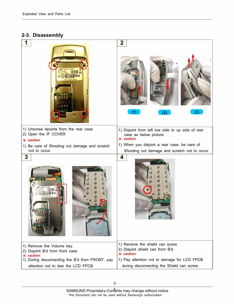
2-3. Disassembly
1
43
2
1) Remove the Volume key.2) Disjoint B'd from front case.caution
1) During disconnecting the B'd from FRONT, pay
attention not to tear the LCD FPCB.
1) Remove the shield can screw2) Disjoint shield can from B'd
caution
1) Pay attention not to damage for LCD FPCB
during disconnecting the Shield can screw.
1) Unscrew 4points from the rear case2) Open the IF COVER
caution
1) Be care of Shooting out damage and scratchnot to occur.
1) Disjoint from left low side to up side of rearcase as below picture.caution
1) When you disjoint a rear case, be care of
Shooting out damage and scratch not to occur.
(1) (2) (3)

SAMSUNG Proprietary-Contents may change without notice
Exploded View and Parts List
2-5
This Document can not be used without Samsung's authorization
5
87
6
1) Remove screw cover using tweezers.2) Unscrew at the folder upper using a screwdriver
caution1) Be care of Shooting out damage and scratch
not to occur.
1) After disjoint the hooker of the lower side,
disassemble the LOWER case as below the
picture.
caution1) Be care of Shooting out damage and scratch
not to occur.
1) Disconnect the LCD connecter and Disjoint the
B'd2) Remove the dust protection tape
caution
1) Be care of Shooting out damage and scratch
not to occur.
2) Pay attention not to damage for LCD FPCB.
1) Pressing the hinge using the rounded tweezersor sort of thing, disjoint FRONT.caution
1) Be care of Shooting out damage and scratch
not to occur.
Press the
hinge
(1)
(2)
(3)

SAMSUNG Proprietary-Contents may change without notice
Exploded View and Parts List
2-
6
This Document can not be used without Samsung's authorization
9 10
1) Remove the Speaker/Motor in the LOWER.2) Remove the LCD in the LOWER.
caution
1) Be care of Speaker/Motor wire cracking or
damage.
1) Check the separated plastics.
caution
1) Check all of the material is taped.

SAMSUNG Proprietary-Contents may change without notice
Exploded View and Parts List
2-7
This Document can not be used without Samsung's authorization
1
43
2
1) Put the LOWER hinge hall to the LCDFPCB, and then put the camera to thePCB.
2) Put the Speaker to the LOWER case,and then arrange the Wire. Put thespeaker to the LOWER case, right sideslightly.caution
1) Be care of SPEAKER/MOTOR wire cracking ordamage.
1) Joint folder hinge side of UPPER case.2) Joint folder UPPER case side and edge.
caution
1) Be care of Shooting out damage and scratch
not to occur.
1) Screw two point of FOLDER Ass'y.2) Assemble the SCREW COVER
caution1) Be care of Shooting out damage and scratch
not to occur.
1) Put the FPCB to the FRONT hole.
2) Pressing the red colored hinge, assemblythe folder and FRONT casecaution
1) Pay attention not to damage for LCD FPCB.
2-4. Assembly
Arrange
the wire

SAMSUNG Proprietary-Contents may change without notice
Exploded View and Parts List
2-
8
This Document can not be used without Samsung's authorization
5
87
6
1) Joint the shield can right hook and
hole of the B'd.2) Screw the left hall of the B'd.caution
1) Pay attention not to damage for LCD FPCB.
1) Joint the FRONT upper hook and B'd and
arrange the B'd, FRONT.2) Attach the Volume Key.
caution
1) Pay attention not to damage for LCD FPCB.
2) Confirm B'd is attached completely on the
FRONT.
1) Attach anti-dust TAPE2) Let a KEY PAD on front assy.
caution
1) Be care of Shooting out damage and scratch
not to occur.
2) Pay attention not to damage for LCD FPCB.
1) Lock a LCD CONNECTOR to PBAcaution
1) Assemble the LCD connect horizontally.
2) Pay attention not to damage for LCD FPCB.
Scwering
joint the
hook
oint the
hook

SAMSUNG Proprietary-Contents may change without notice
Exploded View and Parts List
2-9
This Document can not be used without Samsung's authorization
9 10
1) As below picture, joint the REAR upper
and FRONT and ASS'Y.2) Joint the REAR case side, and then edge.
caution
1) Be care of Shooting out damage and scratch
not to occur.
1) Screw 4 point on REAR assy'.2) Attach the RF COVER.caution
1) Be care of Shooting out damage and scratch
not to occur.
Joint REAR case
and FRONT case.

SAMSUNG Proprietary-Contents may change without notice
Exploded View and Parts List
2-
10
This Document can not be used without Samsung's authorization
1
43
2
1) Attach conduction tape on the left and rightside of LCD.
2) Attach isolation tape on the left and right sideof LCD.caution
1) When you attach the tape, be careful of a base
line of a picture.
1) Attach the SPONGE along the line.2) Attach the isolation tape along the line.
caution
1) When you attach the tape, be careful of a base
line of a picture.
1) Attach CAMERA CONNECTOR sticky isolationtape.
caution
1) When you attach the tape, be careful of a base
line of a picture.
1) Attach the GASKET on the LCD CONNECTOR
caution
1) When you attach the tape, be careful of a base
line of a picture.
(Tape should be in the LCD connect.)
2-5. LCD KIT ASSEMBLING
Attach
conductive
Tape
Attach
isolation Tape
Taping silk
line
Taping silk
line
camera connect
sticky isolation
Tape
SAMSUNG Proprietary-Contents may change without notice
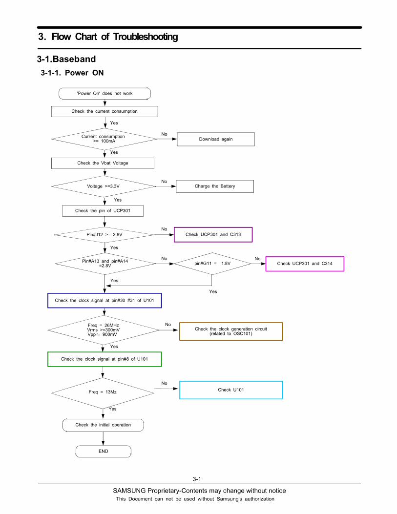
3. Flow Chart of Troubleshooting
3-1
This Document can not be used without Samsung's authorization
3-1.Baseband
3-1-1. Power ON
'Power On' does not work
Voltage >=3.3V
Download again
Charge the Battery
Pin#J12 >= 2.8V Check UCP301 and C313
Pin#A13 and pin#A14=2.8V Check UCP301 and C314
Freq = 26MHzVrms >=300mVVpp 900mV
Check the clock generation circuit(related to OSC101)
Check the initial operation
END
No
Yes
Yes
Yes
Yes
Yes
Yes
No
No
No
No
pin#G11 = 1.8VNo
Yes
Check the current consumption
Check the Vbat Voltage
Check the pin of UCP301
Check the clock signal at pin#30 #31 of U101
Current consumption>= 100mA
Freq = 13Mz
Check the clock signal at pin#8 of U101
Yes
Check U101
No
SAMSUNG Proprietary-Contents may change without notice
Flow Chart of Troubleshooting
3-2
This Document can not be used without Samsung's authorization

SAMSUNG Proprietary-Contents may change without notice
Flow Chart of Troubleshooting
3-3
This Document can not be used without Samsung's authorization
SAMSUNG Proprietary-Contents may change without notice
Flow Chart of Troubleshooting
3-4
This Document can not be used without Samsung's authorization
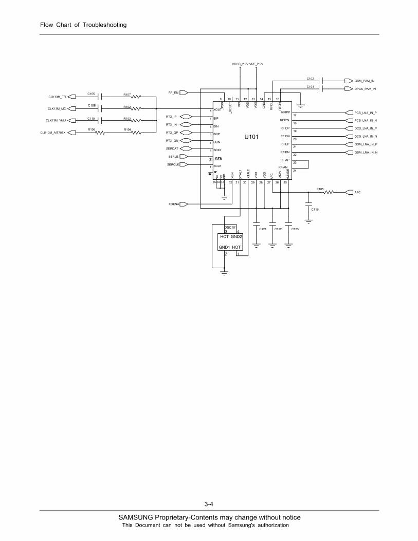
GND1
2
4GND2
1
HOT
HOT3
C104
OSC101
C110
R104
R107
R103
C123C121
R105
C122
C119
C102
R108
C108
C105
R1028
31 30
9 10
VRF_2.9VVCCD_2.9V
13
2829
11
2632 25
XOUT
RFIEN
21RFIEP
18RFIPN
17RFIPP
1615
1 SCLK
3 SDIO
12
333435
24RFIAN
23RFIAP
20RFIDN
19RFIDP
22
U101
27
BIN6
7 BIP
4 BQN
5 BQP
14
CLK13M_MC
CLK13M_AIT701X
RTX_IP
XOENA
GSM_LNA_IN_N
GSM_LNA_IN_P
CLK13M_YMU
CLK13M_TR
DCS_LNA_IN_P
DCS_LNA_IN_N
RF_ENDPCS_PAM_IN
GSM_PAM_IN
AFC
SERDAT
RTX_QN
RTX_QP
RTX_IN
SERCLK
SERLE
PCS_LNA_IN_P
PCS_LNA_IN_N

SAMSUNG Proprietary-Contents may change without notice
Flow Chart of Troubleshooting
3-5
This Document can not be used without Samsung's authorization
3-1-2. Initial
Initial Failure
The pin #G11 of UCP301 =
1.8V and
the pin #J12 of UCP301 =
2.8V ?
Check the UCP301(if it has some problem, it is to be replaced.)
Yes
No
Is the pin #K9 of UCP301
"Low High" ?
Yes
NoCheck the UCP301
(if it has some problem, it is to be replaced.)
There is 32.768kHz wave
forms at the C223 and C224
Yes
No
Check the UCP201
Is the pin #G4 of UCP201
is "High"
The voltage is "High" at the
C311,C312,C313Check the UCP301
Check the UCP201
LCD display is O.K
No
No
Yes
Yes
Yes
Check the LCD part
No
Sound is O.K
Yes
No
Check the Audio part
END
Yes

SAMSUNG Proprietary-Contents may change without notice
Flow Chart of Troubleshooting
3-6
This Document can not be used without Samsung's authorization

SAMSUNG Proprietary-Contents may change without notice
Flow Chart of Troubleshooting
3-7
This Document can not be used without Samsung's authorization
CKO/IACK/ERAMHIIOBIT[2]/VEC[3]/EROMHIIOBIT[1]/VEC[4]/PLLTOA
VCCD_2.9V
VCCD_2.9V
CORE_TP
R208
VCCB_2.9V
R207
VCCD_2.9V
VBAT
C213
VCCD_1.8V VCCD_1.8V
R211
C221R209
C224
R210
XTIC_MODE D12
C223
P15XPA5/WAITN
T15XPA6/BE1N
M9XPA7/IRQ1XPA8/IRQ2
T5P2
XPA9/IRQ3E8
XRTCALARM_N
XPA3/CS4NN14
P16XPA4/OEN
XPA2/CS3NM11
XPA1/CS2NM14M15 XPA0/CS1N
XPA10/IRQ4N2
XCP_WENC13
XOSC32OUTC6
C5D6
XCP_D5E7 XCP_D6
XCP_D7D5C4 XCP_D8B4
XCP_D9B3
XCP_D10XCP_D11
C1C2
XCP_D12
XCP_D13D2D3
XCP_D14E3
XCP_D15
XCP_D2F8F7
XCP_D3
XCP_D4
A16A15
XCP_A7B17 XCP_A8
XCP_A9C17
A13XCP_CSRAMEN
A12 XCP_CSROMEN
A6XCP_D0XCP_D1
B5
K14
L14XCP_A19
E14XCP_A2
L15XCP_A20
L16XCP_A21
XCP_A3D15
XCP_A4B15C14
XCP_A5XCP_A6
D16F14
XCP_A11G14
XCP_A12XCP_A13
G13G17
XCP_A14XCP_A15
J12
XCP_A16K12K13
XCP_A17XCP_A18
XAG0B11A11
XAG1
E11XAG2XAG3
D11
B7XBSWN
M12XCPTSTSTOP_CKO
XCP_A0_BEONB13
XCP_A1F11
XCP_A10
A7X1RTCX2RTC
D10
H13
H12TDI
TDOF12
TMSG12
TRSTF15
N4R12
IO7
K11L12
U5RWN
TCK
R6P6
DB#3DB#4
U7DB#5
T7R7
DB#6DB#7
M6DB#8
P7
N7DB#9
INT#0
P5DB#0
U6DB#1
N8DB#10
DB#11M8U11
DB#12DB#13
T11DB#14
R11P10DB#15
DB#2
AB#3N11P11
AB#4AB#5
P12R14
AB#6
T14AB#7AB#8
T17
G15
UCP201 AB#0 U13M10
AB#1AB#2
R13
DSP_INT
GND2 NC
VCC 41 VOUT
R204
U202
3
R206
C216C215 C214
C222
ZD201
VCCD_1.8V
VRTC_3V
R205
OSC200
AIT_LCD_BY
AIT_SUB_CS
DLC_DETECT
DEBUG_DTRDEBUG_RTSDEBUG_TXDDEBUG_RXDDEBUG_CTS
I2C_CLK
A(23)
BP_VF
AIT_CS
AIT_INT
FLIP_SNSFM_INT
CHG_OFF
EAR_SWITCH
TR_RST
UP_SCLKUP_CS
FLASH_RESET
VREF
ICHRG
AS1
BL_EN
UP_SDO
CHG_DET
SIMRSTPWR_KEEP
SDS_TXD
INTRQ
SDS_RXDSIMDATA
SIMCLK
DSP_IODSP_RWN
DSP_INT
TR_RSTCLK13M_TR
CLK32KRTCALARM
JACK_IN
DEBUG_DSR
TR_RST
CP_TCK
A(21)
UP_SDI
CP_TDOTR_RSTCP_TDICP_TMS
KEY_COL(4)KEY_COL(3)KEY_COL(2)KEY_COL(1)KEY_COL(0)
DSP_AB(8:0)
DSP_AB(7)DSP_AB(6)DSP_AB(5)DSP_AB(4)DSP_AB(3)DSP_AB(2)DSP_AB(1)DSP_AB(0)
KEY_ROW(4)
DSP_AB(8)
YMU_EN
A(22)
CP_CSROMENCP_CSRAMEN
CP_WENCP_OEN
UPPER_BYTE
YMU_IRQ
I2C_DAT
D(3)D(2)D(1)D(0)
A(0:20)
A(20)A(19)A(18)A(17)A(16)A(15)A(14)A(13)A(12)A(11)A(10)A(9)A(8)A(7)A(6)A(5)A(4)A(3)A(2)A(1)A(0)
KEY_ROW(0:4)
KEY_ROW(3)KEY_ROW(2)KEY_ROW(1)KEY_ROW(0)
KEY_COL(0:4)
DSP_DB(15:0)
DSP_DB(0)DSP_DB(1)DSP_DB(2)DSP_DB(3)DSP_DB(4)DSP_DB(5)DSP_DB(6)DSP_DB(7)DSP_DB(8)DSP_DB(9)
DSP_DB(10)DSP_DB(11)DSP_DB(12)DSP_DB(13)DSP_DB(14)DSP_DB(15)
D(0:15)
D(15)D(14)D(13)D(12)D(11)D(10)D(9)D(8)D(7)D(6)D(5)D(4)

SAMSUNG Proprietary-Contents may change without notice
Flow Chart of Troubleshooting
3-8
This Document can not be used without Samsung's authorization
3-1-3. Sim Part
Check the voltage at pin#1of SIM100 >= 2.8V ?
"Insert SIM is displayed on the LCD
Check the SIM connector's(SIM100) connection to
SIM card
Check the UCP301
Resolder or change SIM601
END
No
Yes
Yes
Yes
Yes
No
NoIs there any signals
pin#2,#3,#4 of SIM100 ? Check the UCP301
Check the SIM Card
C642C640C639
G G
8 9
G G
10
1 122
3 34 4
556 6
7
SIM601
C638C641
SIM_IOSIM_RSTVSIM
SIM_CLK

SAMSUNG Proprietary-Contents may change without notice
Flow Chart of Troubleshooting
3-9
This Document can not be used without Samsung's authorization

SAMSUNG Proprietary-Contents may change without notice
Flow Chart of Troubleshooting
3-10
This Document can not be used without Samsung's authorization
3-1-4. Microphone Part
Is the assembled status ofmicrophone O.K?
Microphone does not work
Reassembled the microphone
Resolder or change
R411,R414,C413,C414,C418,C420
C421,R422,C415,C419,R416,R419
R415,R420
END
No
Yes
Yes
Yes
Yes
No
Is microphone ok?
NoCheck UCP301
Check the reference voltage on mic path
VR401 2.0V ?
Yes

SAMSUNG Proprietary-Contents may change without notice
Flow Chart of Troubleshooting
3-11
This Document can not be used without Samsung's authorization
VR401
C420
R419
R416
C414
C419
R415
C413
R422
R414
R411
R420
C415
VR402
C421
C418
VCCA_2.9V
MIC401
MICINP
MICINN
MICOUTN
MICOUTP

SAMSUNG Proprietary-Contents may change without notice
Flow Chart of Troubleshooting
3-12
This Document can not be used without Samsung's authorization
3-1-5. Receiver Part
3-1-6. Speaker Part
There is no sound from the Receiver
Is the terminal of ReceiverO.K ?
No
Replace the Receiver
Yes
No
Yes
Check UCP301
Check V101,V102 (LCD PCB Part)
Is there any signals at thepin#P11 and pin#N12 of
UCP301 ?
END
There is no sound from the Buzzer
Is the terminal of SpeakerO.K ? Replace the Speaker
Is there any signals at thepin#R12 and pin#P12 of
UCP100 ?Check U406,V601,V602
END
Yes
Yes
Yes
Yes
No
No

SAMSUNG Proprietary-Contents may change without notice
Flow Chart of Troubleshooting
3-13
This Document can not be used without Samsung's authorization
< LCD PCB Part >
SAMSUNG Proprietary-Contents may change without notice
Flow Chart of Troubleshooting
3-14
This Document can not be used without Samsung's authorization
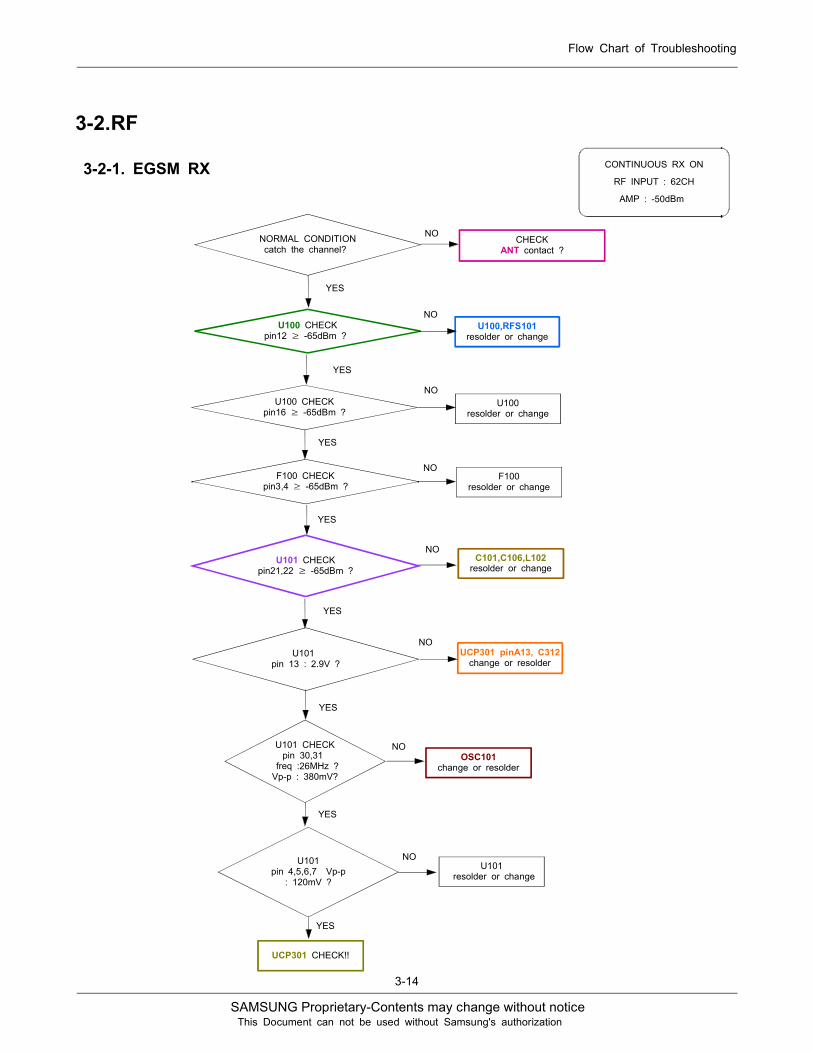
U100 CHECKpin12 -65dBm ?
3-2.RF
3-2-1. EGSM RX CONTINUOUS RX ON
RF INPUT : 62CH
AMP : -50dBm
NORMAL CONDITIONcatch the channel?
CHECKANT contact ?
U101pin 13 : 2.9V ?
U100 CHECKpin16 -65dBm ?
U101 CHECKpin21,22 -65dBm ?
U100,RFS101resolder or change
U100resolder or change
C101,C106,L102resolder or change
UCP301 pinA13, C312change or resolder
U101 CHECKpin 30,31
freq :26MHz ?Vp-p : 380mV?
OSC101change or resolder
U101resolder or change
UCP301 CHECK!!
U101pin 4,5,6,7 Vp-p
: 120mV ?
NO
YES
NO
NO
NO
NO
NO
NO
YES
YES
YES
YES
YES
YES
F100 CHECKpin3,4 -65dBm ?
F100resolder or change
YES
NO

SAMSUNG Proprietary-Contents may change without notice
Flow Chart of Troubleshooting
3-15
This Document can not be used without Samsung's authorization

SAMSUNG Proprietary-Contents may change without notice
Flow Chart of Troubleshooting
3-16
This Document can not be used without Samsung's authorization
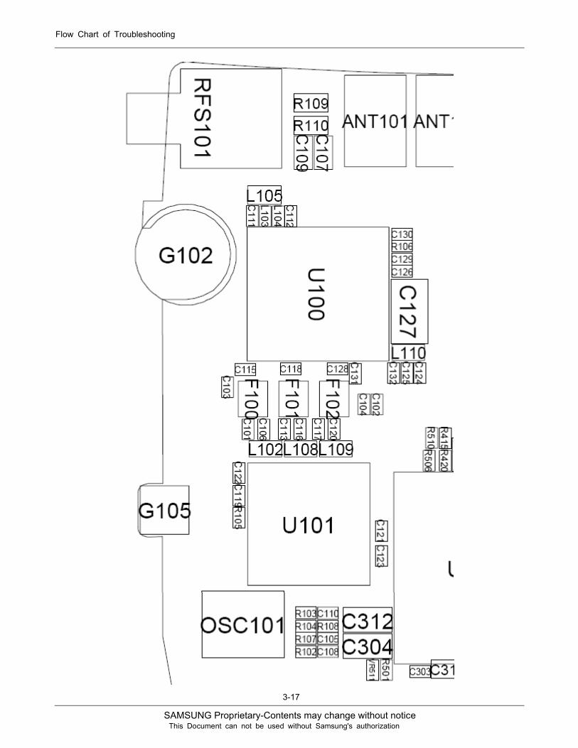
U100 CHECKpin12 -65dBm ?
3-2-2. DCS RXCONTINUOUS RX ON
RF INPUT : 698CH
AMP : -50dBm
YES
NORMAL CONDITIONcatch the channel?
CHECKANT contact ?
U101pin 13 : 2.9V ?
U100 CHECKpin18 -65dBm ?
U101 CHECKpin19,20 -65dBm ?
U100,RFS101resolder or change
U100resolder or change
C13,C116,L108resolder or change
UCP301 pinA13, C312change or resolder
U101 CHECKpin 30,31
freq :26MHz ?Vp-p : 380mV?
OSC101change or resolder
U101resolder or change
UCP301 CHECK!!
U101 pin 4,5,6,7Vp-p
: 120mV ?
NO
YES
NO
NO
NO
NO
NO
YES
YES
YES
YES
YES
F101 CHECKpin3,4 -65dBm ?
F101resolder or change
YES
NO
SAMSUNG Proprietary-Contents may change without notice
Flow Chart of Troubleshooting
3-17
This Document can not be used without Samsung's authorization

SAMSUNG Proprietary-Contents may change without notice
Flow Chart of Troubleshooting
3-18
This Document can not be used without Samsung's authorization
3-2-3. EGSM TX
U100 pin12 :about 2~3 dBm?
C111,RFS101check&change
U100pin6 : 2.8 V?
UCP301check & change
U100pin7 : 3.7 V?
NO NO
YES
YES
NO BATTERYcheck & change
U100pin 8 : 1.6V ?
YES
NO
U100 pin11about : -5dBm ?
YES
U100pin 4 : 2.9V?
YES
YES
U100change or resolder
NO
UCP301check
R106Check
NO
U101pin13 : 2.9V ?
UCP301pinA13,C312change or resolder
YES
U101pin30,31 : 26MHz
?Vp-p : 380mV?
U101pin4,5,6,7 :
100mV?
YES
UCP301change or resolder
NO
NO
U101change or resolder
YES
NOOSC101
change or resolder
CONTINOUS TX ON CONDITIONTX POWER DAC: 600 CODE APPLIED
CH : 62RBW : 100KHzVBW : 100KHzSPAN : 10MHz
REF LEV. : 10dBmATT. : 20dB

SAMSUNG Proprietary-Contents may change without notice
Flow Chart of Troubleshooting
3-19
This Document can not be used without Samsung's authorization
SAMSUNG Proprietary-Contents may change without notice
Flow Chart of Troubleshooting
3-20
This Document can not be used without Samsung's authorization
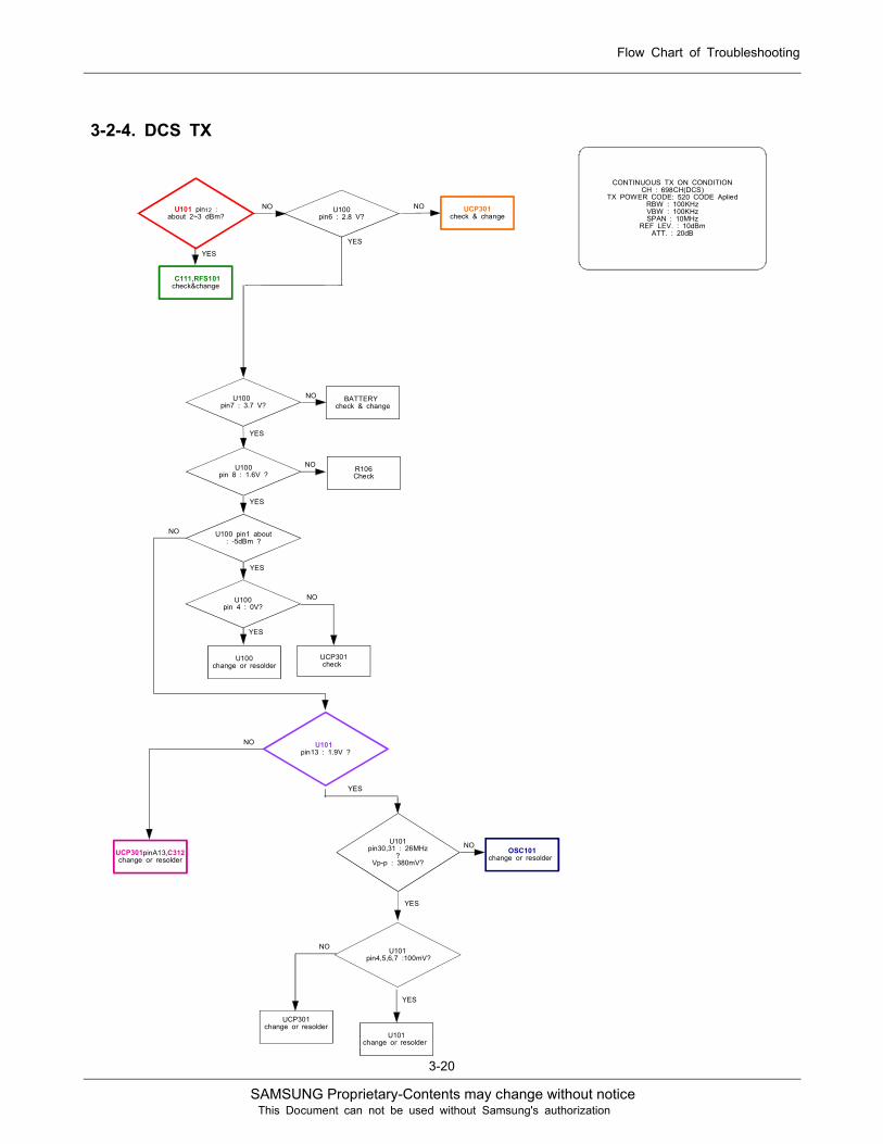
3-2-4. DCS TX
CONTINUOUS TX ON CONDITIONCH : 698CH(DCS)
TX POWER CODE: 520 CODE ApliedRBW : 100KHzVBW : 100KHzSPAN : 10MHz
REF LEV. : 10dBmATT. : 20dB
U101 pin12 :about 2~3 dBm?
C111,RFS101check&change
U100pin6 : 2.8 V?
UCP301check & change
U100pin7 : 3.7 V?
NO NO
YES
YES
NO BATTERYcheck & change
U100pin 8 : 1.6V ?
YES
NO
U100 pin1 about: -5dBm ?
YES
U100pin 4 : 0V?
YES
YES
U100change or resolder
NO
UCP301check
R106Check
NO
U101pin13 : 1.9V ?
UCP301pinA13,C312change or resolder
YES
U101pin30,31 : 26MHz
?Vp-p : 380mV?
U101pin4,5,6,7 :100mV?
YES
UCP301change or resolder
NO
NO
YES
NOOSC101
change or resolder
U101change or resolder

SAMSUNG Proprietary-Contents may change without notice
Flow Chart of Troubleshooting
3-21
This Document can not be used without Samsung's authorization

SAMSUNG Proprietary-Contents may change without notice
Flow Chart of Troubleshooting
3-22
This Document can not be used without Samsung's authorization
11
2 23 3
44
55
66
L104
ANT102
C107
C131
C115
2
G
5
1IN
OUT3
OUT4
F102
G
C106
R106
C124
1IN
OUT3
4OUT
VBAT
C125
F100
G
2
G
5
C118
C128
RFS101
C127
L103
C111
R109
L102
L105
C112
11
223
34
45
5
66
R110
ANT101
L109
L108
C109
C132C130C129
C126
F101
G
2
G
5
1IN
OUT3
4OUT
C116
C113
VCC1
VCC2
V113 GND115 GND217 GND319 GND421 GND5
U100
C103
L110
C120
C117
C101
DCS_LNA_IN_N
DCS_LNA_IN_P
ANT
BAND_SEL1BAND_SEL2VMOD_EN
GSM_LNA_IN_P
GSM_LNA_IN_N
PCS_LNA_IN_P
PCS_LNA_IN_N
TX_PWRTX_EN
DPCS_PAM_IN
GSM_PAM_IN

SAMSUNG Proprietary-Contents may change without notice
Flow Chart of Troubleshooting
3-23
This Document can not be used without Samsung's authorization
GND1
2
4GND2
1
HOT
HOT3
C104
OSC101
C110
R104
R107
R103
C123C121
R105
C122
C119
C102
R108
C108
C105
R1028
31 30
9 10
VRF_2.9VVCCD_2.9V
13
2829
11
2632 25
XOUT
RFIEN
21RFIEP
18RFIPN
17RFIPP
1615
1 SCLK
3 SDIO
12
333435
24RFIAN
23RFIAP
20RFIDN
19RFIDP
22
U101
27
BIN6
7 BIP
4 BQN
5 BQP
14
CLK13M_MC
CLK13M_AIT701X
RTX_IP
XOENA
GSM_LNA_IN_N
GSM_LNA_IN_P
CLK13M_YMU
CLK13M_TR
DCS_LNA_IN_P
DCS_LNA_IN_N
RF_ENDPCS_PAM_IN
GSM_PAM_IN
AFC
SERDAT
RTX_QN
RTX_QP
RTX_IN
SERCLK
SERLE
PCS_LNA_IN_P
PCS_LNA_IN_N
SAMSUNG Proprietary-Contents may change without notice
4. Array course control
4-1
This Document can not be used without Samsung's authorization

SAMSUNG Proprietary-Contents may change without notice
Array course control
4-2
This Document can not be used without Samsung's authorization
Software Downloading
4-1. Downloading Binary FilesThree binary files for downloading M300- M300XXYY.s3 : Main source code binary
4-2. Pre-requsite for DownloadingDownloader Program(OptiFlash.exe)M300 Mobile PhoneData CableBinary files

SAMSUNG Proprietary-Contents may change without notice
Array course control
4-3
This Document can not be used without Samsung's authorization
4-3. S/W Downloader Program
1. Load the binary download program by executing the "Optiflash.exe"
2. Select the "Options" "Settings" "Generic" "Specify hardwareplatform".
Choose hardware platform for the downloader file setting.Set the everything else as the default values which are shown below

SAMSUNG Proprietary-Contents may change without notice
Array course control
4-4
This Document can not be used without Samsung's authorization
3.Select the COM port when the download cable is connected
Additionally you can select the maximum transfer speed OptiFlash will use tocommunicate with the phone. However, OptiFlash will use a slower speed ifeither the PC's or the phone's serial hardware is incapable of handling theselected speed

SAMSUNG Proprietary-Contents may change without notice
Array course control
4-5
This Document can not be used without Samsung's authorization
4. Select the "Flash&Verify" "Browse"Set the directory path and choose the lastet s/w binary, for example"M300XXYY.s3", for the downloader binary setting.
Make sure that not to change the reserved memory regions.In case of M300 the reserved regions are :- 0x00008000 - 0x0001ffff

SAMSUNG Proprietary-Contents may change without notice
Array course control
4-6
This Document can not be used without Samsung's authorization
5. Click "OK" button then press "Flash".(Before pressing 'Flash' button, push the button '*'and 'END' at the sametime. Then press 'Flash'.)
Downloader will upload the binary file as below for the downloading.
6. When downloading is finished successfully, there is a "All is well" message.
7. After finishing downloading, Certain memory resets should be done toguarantee the normal performance.
8. Confirm the downloaded version name and etc. :*#1234#
Full Reset :*2767*3855#

SAMSUNG Proprietary-Contents may change without notice
5. Block Diagrams
5-1
This Document can not be used without Samsung's authorization

SAMSUNG Proprietary-Contents may change without notice
Block Diagrams
5-2
This Document can not be used without Samsung's authorization

6. PCB Diagrams
6-
ANT101 ANT102
BTC601
C224
CORE_TPCP_CSRAMCP_OEN
CP_TCK
CP_TDICP_TDO
CP_TMS
CP_WEN
DSP_INT
G101G102
G103G104
G105
IFC601
MIC401
OSC101
RST
SIM601TA501
TP201TP202 TP203TP204TP205
TP_A(1)
TP_AIT_CS
TP_AIT_INT
TP_CSROM
TP_D(0)
TP_GND
TP_INTRQ TP_PWR_KEEP
TP_UPPER_BY TE
U101
U203
U301
U302
U402
U403
U404
U501
UCP301
VR401
VR502
VR503
VR505
VR510
ZD201
ZD501
ZD601ZD602
ZD603

PCB Diagrams
6-
*
1
10
23
45
6
78
9
CLEAR
DOWN
I
LED301 LED302
PWR
SHARP
U201
UP
SAMSUNG Proprietary-Contents may change without notice
7. MAIN Electrical Parts List
7-1
This Document can not be used without Samsung's authorization
SEC CODE Design LOC Discirption STATUS
0403-001547 ZD603 DIODE-ZENER SA
0406-001190 ZD601 DIODE-TVS SA
0406-001219 ZD602 DIODE-TVS SA
0406-001223 ZD604 DIODE-TVS SA
0406-001231 ZD201 DIODE-TVS SA
0406-001260 ZD501 DIODE-TVS SA
0504-001113 TR301 TR-DIGITAL SA
0601-002268 LED301 LED SA
0601-002268 LED302 LED SA
0801-002529 U302 IC-CMOS LOGIC SA
1001-001394 U404 IC-ANALOG SWITCH SA
1001-001428 U405 IC-ANALOG MULTIPLEX SA
1001-001428 U601 IC-ANALOG MULTIPLEX SA
1001-001428 U602 IC-ANALOG MULTIPLEX SA
1001-001459 U403 IC-ANALOG SWITCH SA
1009-001020 U201 IC-HALL EFFECT S/W SA
1108-000010 UME201 IC-MCP SA
1201-002180 U402 IC-AUDIO AMP SA
1201-002278 U100 IC-POWER AMP SA
1203-003304 UCP301 IC-POWER SUPERVISOR SA
1203-003663 U301 IC-BATTERY SA
1204-001811 U406 IC-MELODY SA
1204-002700 U401 IC-TUNER SA
1205-003116 U101 IC-TRANSCEIVER SA
1209-001712 U202 IC-SENSOR SA
1405-001082 V601 VARISTOR SA
1405-001082 V602 VARISTOR SA
1405-001082 VR401 VARISTOR SA
1405-001082 VR402 VARISTOR SA
1405-001082 VR503 VARISTOR SA
1405-001082 VR510 VARISTOR SA
1405-001177 V603 VARISTOR SA
1405-001177 V604 VARISTOR SA
1405-001177 V605 VARISTOR SA
1405-001177 VR501 VARISTOR SA
1405-001177 VR502 VARISTOR SA

SAMSUNG Proprietary-Contents may change without notice
Main Electrical Parts List
7-2
This Document can not be used without Samsung's authorization
SEC CODE Design LOC Discirption STATUS
1405-001177 VR504 VARISTOR SA
1405-001177 VR505 VARISTOR SA
1405-001177 VR506 VARISTOR SA
1405-001177 VR507 VARISTOR SA
1405-001177 VR508 VARISTOR SA
1405-001177 VR509 VARISTOR SA
1405-001177 VR511 VARISTOR SA
2007-000144 R305 R-CHIP SA
2007-000148 R406 R-CHIP SA
2007-000148 R407 R-CHIP SA
2007-000162 R203 R-CHIP SA
2007-000162 R206 R-CHIP SA
2007-000170 R209 R-CHIP SA
2007-000171 R109 R-CHIP SA
2007-000171 R110 R-CHIP SA
2007-000172 R311 R-CHIP SA
2007-000172 R312 R-CHIP SA
2007-000173 R417 R-CHIP SA
2007-000173 R418 R-CHIP SA
2007-000831 R620 R-CHIP SA
2007-001244 R309 R-CHIP SA
2007-007101 R425 R-CHIP SA
2007-007134 R404 R-CHIP SA
2007-007134 R405 R-CHIP SA
2007-007138 R302 R-CHIP SA
2007-007573 R207 R-CHIP SA
2007-007573 R208 R-CHIP SA
2007-007741 R416 R-CHIP SA
2007-007741 R419 R-CHIP SA
2007-007741 R507 R-CHIP SA
2007-007741 R509 R-CHIP SA
2007-008045 R103 R-CHIP SA
2007-008048 R102 R-CHIP SA
2007-008051 R427 R-CHIP SA
2007-008052 R210 R-CHIP SA
2007-008052 R211 R-CHIP SA
SAMSUNG Proprietary-Contents may change without notice
Main Electrical Parts List
7-3
This Document can not be used without Samsung's authorization
SEC CODE Design LOC Discirption STATUS
2007-008055 R301 R-CHIP SA
2007-008055 R308 R-CHIP SA
2007-008055 R401 R-CHIP SA
2007-008419 R613 R-CHIP SA
2007-008419 R614 R-CHIP SA
2007-008419 R615 R-CHIP SA
2007-008419 R616 R-CHIP SA
2007-008419 R617 R-CHIP SA
2007-008419 R618 R-CHIP SA
2007-008419 R619 R-CHIP SA
2007-008483 R205 R-CHIP SA
2007-008483 R303 R-CHIP SA
2007-008483 R403 R-CHIP SA
2007-008483 R408 R-CHIP SA
2007-008483 R410 R-CHIP SA
2007-008483 R412 R-CHIP SA
2007-008483 R603 R-CHIP SA
2007-008486 R606 R-CHIP SA
2007-008486 R607 R-CHIP SA
2007-008486 R609 R-CHIP SA
2007-008486 R610 R-CHIP SA
2007-008516 R105 R-CHIP SA
2007-008516 R106 R-CHIP SA
2007-008531 R201 R-CHIP SA
2007-008531 R202 R-CHIP SA
2007-008531 R501 R-CHIP SA
2007-008542 R104 R-CHIP SA
2007-008542 R108 R-CHIP SA
2007-008542 R402 R-CHIP SA
2007-008542 R429 R-CHIP SA
2007-008544 R411 R-CHIP SA
2007-008544 R504 R-CHIP SA
2007-008587 R107 R-CHIP SA
2007-008786 R424 R-CHIP SA
2007-008786 R426 R-CHIP SA
2007-008786 R428 R-CHIP SA

SAMSUNG Proprietary-Contents may change without notice
Main Electrical Parts List
7-4
This Document can not be used without Samsung's authorization
SEC CODE Design LOC Discirption STATUS
2007-008788 R621 R-CHIP SA
2007-008788 R622 R-CHIP SA
2007-008808 R506 R-CHIP SA
2007-008808 R510 R-CHIP SA
2007-009108 R423 R-CHIP SA
2007-009157 R415 R-CHIP SA
2007-009157 R420 R-CHIP SA
2007-009160 R304 R-CHIP SA
2007-009168 R307 R-CHIP SA
2007-009170 R611 R-CHIP SA
2007-009171 R602 R-CHIP SA
2007-009171 R604 R-CHIP SA
2007-009194 R601 R-CHIP SNA
2007-009315 R204 R-CHIP SA
2007-009402 R414 R-CHIP SA
2007-009402 R505 R-CHIP SA
2007-009408 R422 R-CHIP SA
2007-009408 R511 R-CHIP SA
2203-000233 C222 C-CER,CHIP SA
2203-000233 C315 C-CER,CHIP SA
2203-000233 C402 C-CER,CHIP SA
2203-000359 C420 C-CER,CHIP SA
2203-000359 C421 C-CER,CHIP SA
2203-000438 C429 C-CER,CHIP SA
2203-000654 C427 C-CER,CHIP SA
2203-000995 C207 C-CER,CHIP SA
2203-002709 C643 C-CER,CHIP SA
2203-005682 C104 C-CER,CHIP SA
2203-005682 C108 C-CER,CHIP SA
2203-005682 C128 C-CER,CHIP SA
2203-005682 C130 C-CER,CHIP SA
2203-005682 C131 C-CER,CHIP SA
2203-005682 C132 C-CER,CHIP SA
2203-005682 C423 C-CER,CHIP SA
2203-005682 C424 C-CER,CHIP SA
2203-005682 C509 C-CER,CHIP SA

SAMSUNG Proprietary-Contents may change without notice
Main Electrical Parts List
7-5
This Document can not be used without Samsung's authorization
SEC CODE Design LOC Discirption STATUS
2203-005682 C641 C-CER,CHIP SA
2203-005682 C642 C-CER,CHIP SA
2203-005683 C418 C-CER,CHIP SA
2203-005683 C614 C-CER,CHIP SA
2203-005683 C631 C-CER,CHIP SA
2203-005717 C215 C-CER,CHIP SA
2203-005725 C223 C-CER,CHIP SA
2203-005725 C224 C-CER,CHIP SA
2203-005725 C626 C-CER,CHIP SA
2203-005725 C627 C-CER,CHIP SA
2203-005729 C105 C-CER,CHIP SA
2203-005731 C103 C-CER,CHIP SA
2203-005736 C115 C-CER,CHIP SA
2203-005736 C118 C-CER,CHIP SA
2203-005736 C129 C-CER,CHIP SA
2203-005777 C101 C-CER,CHIP SA
2203-005777 C106 C-CER,CHIP SA
2203-005777 C112 C-CER,CHIP SA
2203-006048 C416 C-CER,CHIP SA
2203-006048 C428 C-CER,CHIP SA
2203-006121 C640 C-CER,CHIP SA
2203-006194 C110 C-CER,CHIP SA
2203-006194 C119 C-CER,CHIP SA
2203-006194 C124 C-CER,CHIP SA
2203-006257 C414 C-CER,CHIP SA
2203-006257 C506 C-CER,CHIP SA
2203-006260 C203 C-CER,CHIP SA
2203-006260 C212 C-CER,CHIP SA
2203-006307 C307 C-CER,CHIP SA
2203-006318 C113 C-CER,CHIP SA
2203-006318 C116 C-CER,CHIP SA
2203-006318 C117 C-CER,CHIP SA
2203-006318 C120 C-CER,CHIP SA
2203-006324 C304 C-CER,CHIP SA
2203-006423 C121 C-CER,CHIP SA
2203-006423 C123 C-CER,CHIP SA
SAMSUNG Proprietary-Contents may change without notice
Main Electrical Parts List
7-6
This Document can not be used without Samsung's authorization
SEC CODE Design LOC Discirption STATUS
2203-006423 C125 C-CER,CHIP SA
2203-006423 C126 C-CER,CHIP SA
2203-006423 C206 C-CER,CHIP SA
2203-006423 C208 C-CER,CHIP SA
2203-006423 C210 C-CER,CHIP SA
2203-006423 C214 C-CER,CHIP SA
2203-006423 C217 C-CER,CHIP SA
2203-006423 C218 C-CER,CHIP SA
2203-006423 C219 C-CER,CHIP SA
2203-006423 C220 C-CER,CHIP SA
2203-006423 C221 C-CER,CHIP SA
2203-006423 C301 C-CER,CHIP SA
2203-006423 C319 C-CER,CHIP SA
2203-006423 C408 C-CER,CHIP SA
2203-006423 C431 C-CER,CHIP SA
2203-006423 C502 C-CER,CHIP SA
2203-006423 C503 C-CER,CHIP SA
2203-006423 C615 C-CER,CHIP SA
2203-006423 C630 C-CER,CHIP SA
2203-006423 C639 C-CER,CHIP SA
2203-006462 C425 C-CER,CHIP SA
2203-006556 C102 C-CER,CHIP SA
2203-006556 C111 C-CER,CHIP SA
2203-006556 C601 C-CER,CHIP SA
2203-006556 C602 C-CER,CHIP SA
2203-006556 C603 C-CER,CHIP SA
2203-006556 C604 C-CER,CHIP SA
2203-006556 C605 C-CER,CHIP SA
2203-006556 C606 C-CER,CHIP SA
2203-006556 C607 C-CER,CHIP SA
2203-006556 C608 C-CER,CHIP SA
2203-006556 C609 C-CER,CHIP SA
2203-006556 C610 C-CER,CHIP SA
2203-006556 C611 C-CER,CHIP SA
2203-006556 C612 C-CER,CHIP SA
2203-006556 C613 C-CER,CHIP SA

SAMSUNG Proprietary-Contents may change without notice
Main Electrical Parts List
7-7
This Document can not be used without Samsung's authorization
SEC CODE Design LOC Discirption STATUS
2203-006556 C617 C-CER,CHIP SA
2203-006556 C618 C-CER,CHIP SA
2203-006556 C619 C-CER,CHIP SA
2203-006556 C620 C-CER,CHIP SA
2203-006556 C621 C-CER,CHIP SA
2203-006556 C622 C-CER,CHIP SA
2203-006556 C623 C-CER,CHIP SA
2203-006556 C624 C-CER,CHIP SA
2203-006556 C625 C-CER,CHIP SA
2203-006556 C628 C-CER,CHIP SA
2203-006556 C629 C-CER,CHIP SA
2203-006556 C638 C-CER,CHIP SA
2203-006562 C306 C-CER,CHIP SA
2203-006562 C308 C-CER,CHIP SA
2203-006562 C309 C-CER,CHIP SA
2203-006562 C310 C-CER,CHIP SA
2203-006562 C311 C-CER,CHIP SA
2203-006562 C313 C-CER,CHIP SA
2203-006562 C316 C-CER,CHIP SA
2203-006562 C318 C-CER,CHIP SA
2203-006562 C401 C-CER,CHIP SA
2203-006562 C403 C-CER,CHIP SA
2203-006562 C404 C-CER,CHIP SA
2203-006562 C405 C-CER,CHIP SA
2203-006562 C406 C-CER,CHIP SA
2203-006562 C407 C-CER,CHIP SA
2203-006562 C410 C-CER,CHIP SA
2203-006562 C411 C-CER,CHIP SA
2203-006562 C412 C-CER,CHIP SA
2203-006562 C422 C-CER,CHIP SA
2203-006562 C434 C-CER,CHIP SA
2203-006562 C501 C-CER,CHIP SA
2203-006562 C504 C-CER,CHIP SA
2203-006562 C616 C-CER,CHIP SA
2203-006562 C635 C-CER,CHIP SA
2203-006562 C644 C-CER,CHIP SA

SAMSUNG Proprietary-Contents may change without notice
Main Electrical Parts List
7-8
This Document can not be used without Samsung's authorization
SEC CODE Design LOC Discirption STATUS
2203-006626 C507 C-CER,CHIP SA
2203-006626 C508 C-CER,CHIP SA
2203-006648 C122 C-CER,CHIP SA
2203-006648 C216 C-CER,CHIP SA
2203-006648 C317 C-CER,CHIP SA
2203-006648 C409 C-CER,CHIP SA
2203-006648 C426 C-CER,CHIP SA
2203-006648 C636 C-CER,CHIP SA
2203-006824 C312 C-CER,CHIP SA
2203-006824 C314 C-CER,CHIP SA
2203-006824 C417 C-CER,CHIP SA
2203-006824 C430 C-CER,CHIP SA
2203-006872 C432 C-CER,CHIP SA
2203-006872 C433 C-CER,CHIP SA
2203-006979 C201 C-CER,CHIP SA
2203-006979 C202 C-CER,CHIP SA
2203-006979 C204 C-CER,CHIP SA
2203-006979 C205 C-CER,CHIP SA
2203-006979 C209 C-CER,CHIP SA
2203-006979 C211 C-CER,CHIP SA
2203-006979 C213 C-CER,CHIP SA
2203-006979 C302 C-CER,CHIP SA
2203-006979 C303 C-CER,CHIP SA
2203-007143 C415 C-CER,CHIP SA
2203-007143 C419 C-CER,CHIP SA
2404-001374 C127 C-TA,CHIP SA
2404-001381 TA601 C-TA,CHIP SA
2404-001414 C413 C-TA,CHIP SA
2404-001414 TA501 C-TA,CHIP SA
2703-002313 L105 INDUCTOR-SMD SA
2703-002485 L102 INDUCTOR-SMD SA
2703-002544 L108 INDUCTOR-SMD SA
2703-002544 L109 INDUCTOR-SMD SA
2703-002558 L110 INDUCTOR-SMD SA
2703-002917 L103 INDUCTOR-SMD SA
2703-002917 L104 INDUCTOR-SMD SA

SAMSUNG Proprietary-Contents may change without notice
Main Electrical Parts List
7-9
This Document can not be used without Samsung's authorization
SEC CODE Design LOC Discirption STATUS
2703-003196 L603 INDUCTOR-SMD SA
2801-004373 OSC200 CRYSTAL-SMD SA
2801-004587 OSC101 CRYSTAL-SMD SA
2904-001592 F100 FILTER-SAW SA
2904-001599 F101 FILTER-SAW SA
2904-001600 F102 FILTER-SAW SA
3301-001342 L201 BEAD-SMD SA
3301-001659 L403 BEAD-SMD SA
3301-001729 L401 BEAD-SMD SA
3301-001729 L402 BEAD-SMD SA
3301-001729 L601 BEAD-SMD SA
3301-001729 L602 BEAD-SMD SA
3404-001303 SW501 SWITCH-TACT SA
3404-001303 SW502 SWITCH-TACT SA
3705-001242 RFS101 CONNECTOR-COAXIAL SA
3709-001488 SIM601 CONNECTOR-CARD EDGE SA
3710-002442 IFC601 SOCKET-INTERFACE SA
3711-006026 BTC601 HEADER-BATTERY SA
3711-006380 HEA601 HEADER-BOARD TO BOARD SA
4302-001130 BAT101 BATTERY-LI(2ND) SA
GH09-00036A UCP201 IC MICOM-SGHX480 SA
GH13-00050A U501 IC ASIC-SGHC510 SA
GH71-06419A ANT101 NPR-ANTENNA CONTACT SA
GH71-06419A ANT102 NPR-ANTENNA CONTACT SA

SAMSUNG Proprietary-Contents may change without notice
8. Reference data
8-1
This Document can not be used without Samsung's authorization
8-1. Reference Abbreviate
AAC: Advanced Audio Coding.
AVC : Advanced Video Coding.
BER : Bit Error Rate
BPSK: Binary Phase Shift Keying
CA : Conditional Access
CDM : Code Division Multiplexing
C/I : Carrier to Interference
DMB : Digital Multimedia Broadcasting
EN : European Standard
ES : Elementary Stream
ETSI: European Telecommunications Standards Institute
MPEG: Moving Picture Experts Group
PN : Pseudo-random Noise
PS : Pilot Symbol
QPSK: Quadrature Phase Shift Keying
RS : Reed-Solomon
SI : Service Information
TDM : Time Division Multiplexing
TS : Transport Stream

SAMSUNG Proprietary-Contents may change without notice
9. Safety Precautions
9-1
This Document can not be used without Samsung's authorization
9-1. Repair Precaution
Repair in Shield Box, during detailed tuning.
Take specially care of tuning or test,
because specipicty of cellular phone is sensitive for surrounding interference(RF noise).
Be careful to use a kind of magnetic object or tool,
because performance of parts is damaged by the influence of manetic force.
Surely use a standard screwdriver when you disassemble this product,
otherwise screw will be worn away.
Use a thicken twisted wire when you measure level.
A thicken twisted wire has low resistance, therefore error of measurement is few.
Repair after separate Test Pack and Set because for short danger (for example an
overcurrent and furious flames of parts etc) when you repair board in condition of
connecting Test Pack and tuning on.
Take specially care of soldering, because Land of PCB is small and weak in heat.
Surely tune on/off while using AC power plug, because a repair of battery charger is
dangerous when tuning ON/OFF PBA and Connector after disassembing charger.
Don't use as you pleases after change other material than replacement registered on SEC
System. Otherwise engineer in charge isn't charged with problem that you don't keep this
rules.

SAMSUNG Proprietary-Contents may change without notice
Safety Precautions
9-2
This Document can not be used without Samsung's authorization
9-2. ESD(Electrostatically Sensitive Devices) Precaution
Several semiconductor may be damaged easilly by static electricity. Such parts are called by
ESD(Electrostatically Sensitive Devices), for example IC,BGA chip etc. Read Precaution below.
You can prevent from ESD damage by static electricity.
Remove static electricity remained your body before you touch semiconductor or parts with
semiconductor. There are ways that you touch an earthed place or wear static electricity
prevention string on wrist.
Use earthed soldering steel when you connect or disconnect ESD.
Use soldering removing tool to break static electricity. , otherwise ESD will be damaged by
static electricity.
Don't unpack until you set up ESD on product. Because most of ESD are packed by box
and aluminum plate to have conductive power,they are prevented from static electricity.
You must maintain electric contact between ESD and place due to be set up until ESD is
connected completely to the proper place or a circuit board.

SAMSUNG Proprietary-Contents may change without notice
10. Product Function
10-1
This Document can not be used without Samsung's authorization
Main Function- SDN (Service Dialling Numbers)
- Read SMS or MMS messages
- Voicemail
- SOS message
- FM radio
This Service Manual is a property of Samsung Electronics Co.,Ltd.Any unauthorized use of Manual can be punished under applicableInternational and/or domestic law.
Samsung Electronics Co.,Ltd.
2007. 05. Rev.1.0
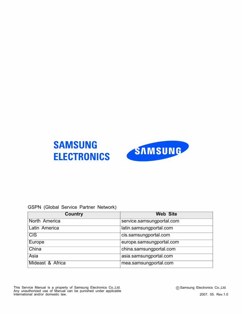
Country Web Site
North America service.samsungportal.com
Latin America latin.samsungportal.com
CIS cis.samsungportal.com
Europe europe.samsungportal.com
China china.samsungportal.com
Asia asia.samsungportal.com
Mideast & Africa mea.samsungportal.com
GSPN (Global Service Partner Network)


![Home [] · 2021. 2. 24. · samsung samsung samsung samsung samsung advance advance advance advance advance advance advance advance advance advance 223sw 2233sw 2233sw 2233sw 933sn](https://static.fdocuments.net/doc/165x107/613cd1974c23507cb6359ff0/home-2021-2-24-samsung-samsung-samsung-samsung-samsung-advance-advance.jpg)