S1C17 Family Application Note S1C17M01/W22/W23 … · S1C17 Family Application Note . S1C17M01/W22...
51
S1C17 Family Application Note S1C17M01/W22/W23 Peripheral Circuit Sample Software
-
Upload
phamnguyet -
Category
Documents
-
view
230 -
download
0
Transcript of S1C17 Family Application Note S1C17M01/W22/W23 … · S1C17 Family Application Note . S1C17M01/W22...

S1C17 Family Application Note
S1C17M01/W22/W23 Peripheral Circuit Sample
Software
Evaluation board/kit and Development tool important notice 1. This evaluation board/kit or development tool is designed for use for engineering evaluation, demonstration,
or development purposes only. Do not use it for other purposes. It is not intended to meet the requirements of design for finished products.
2. This evaluation board/kit or development tool is intended for use by an electronics engineer and is not a consumer product. The user should use it properly and in a safe manner. Seiko Epson dose not assume any responsibility or liability of any kind of damage and/or fire coursed by the use of it. The user should cease to use it when any abnormal issue occurs even during proper and safe use.
3. The part used for this evaluation board/kit or development tool may be changed without any notice. NOTICE No part of this material may be reproduced or duplicated in any form or by any means without the written permission of Seiko Epson. Seiko Epson reserves the right to make changes to this material without notice. Seiko Epson does not assume any liability of any kind arising out of any inaccuracies contained in this material or due to its application or use in any product or circuit and, further, there is no representation that this material is applicable to products requiring high level reliability, such as, medical products. Moreover, no license to any intellectual property rights is granted by implication or otherwise, and there is no representation or warranty that anything made in accordance with this material will be free from any patent or copyright infringement of a third party. When exporting the products or technology described in this material, you should comply with the applicable export control laws and regulations and follow the procedures required by such laws and regulations. You are requested not to use, to resell, to export and/or to otherwise dispose of the products (and any technical information furnished, if any) for the development and/or manufacture of weapon of mass destruction or for other military purposes. All brands or product names mentioned herein are trademarks and/or registered trademarks of their respective companies.
©SEIKO EPSON CORPORATION 2015, All rights reserved.
S1C17M01/W22/W23 Peripheral Circuit Seiko Epson Corporation i Sample Software (Rev.1.2)
Table of Contents
1. Overview ....................................................................................................................1
1.1 Operating Environment ......................................................................................................... 1
2. Sample Software Configuration ................................................................................2
2.1 Directory Structure and File Composition ............................................................................ 2
3. Execution Method ......................................................................................................4
3.1 Software Development Environment .................................................................................... 4 3.2 Installing each Tool ................................................................................................................ 4 3.3 Importing Project ................................................................................................................... 5
3.3.1 Importing Sample Program (Common to GNU17 version 2 and version 3) ......................... 5 3.3.2 Importing Sample Program (GNU17 version 2) .................................................................. 7 3.3.3 Importing Sample Program (GNU17 version 3) ................................................................ 11
3.4 Connecting with Target ........................................................................................................ 15 3.5 Operating ICDmini and Target ............................................................................................. 16
3.5.1 When ICDmini ver. 2.0 is Used ........................................................................................ 16 3.5.2 When ICDmini ver. 3.0 is Used ........................................................................................ 17
3.6 Building Project and Starting Debugger ............................................................................. 18 3.6.1 When GNU17 version 2 is Used ...................................................................................... 18 3.6.2 When GNU17 version 3 is Used ...................................................................................... 19
4. Details of Sample Software Function .....................................................................20
4.1 I/O Port (P) [Common to S1C17M01/W22/W23] .................................................................. 20 4.1.1 Sample Software Specification ........................................................................................ 20 4.1.2 Hardware Conditions ....................................................................................................... 20 4.1.3 Operations Overview ....................................................................................................... 21
4.2 Clock Generator (CLG) [Common to S1C17M01/W22/W23] ............................................... 22 4.2.1 Sample Software Specification ........................................................................................ 22 4.2.2 Hardware Conditions ....................................................................................................... 22 4.2.3 Operations Overview (S1C17M01) .................................................................................. 22 4.2.4 Operations Overview (S1C17W22/W23) .......................................................................... 24
4.3 16-Bit Timer (T16) [Common to S1C17M01/W22/W23] ....................................................... 26 4.3.1 Sample Software Specification ........................................................................................ 26 4.3.2 Hardware Conditions ....................................................................................................... 26 4.3.3 Operations Overview ....................................................................................................... 26
4.4 16-Bit PWM Timer (T16B) [Only for S1C17W22/W23] ......................................................... 27 4.4.1 Sample Software Specification ........................................................................................ 27 4.4.2 Hardware Conditions ....................................................................................................... 27 4.4.3 Operations Overview ....................................................................................................... 27
4.5 Real Time Clock (RTCA) [Common to S1C17M01/W22/W23] ............................................. 29 4.5.1 Sample Software Specification ........................................................................................ 29 4.5.2 Hardware Conditions ....................................................................................................... 29 4.5.3 Operations Overview ....................................................................................................... 29
4.6 Watchdog Timer (WDT) [Common to S1C17M01/W22/W23] .............................................. 30 4.6.1 Sample Software Specification ........................................................................................ 30 4.6.2 Hardware Conditions ....................................................................................................... 30 4.6.3 Operations Overview ....................................................................................................... 30
4.7 UART (UART) [Common to S1C17M01/W22/W23] .............................................................. 31 4.7.1 Sample Software Specification ........................................................................................ 31 4.7.2 Hardware Conditions ....................................................................................................... 31 4.7.3 Operations Overview ....................................................................................................... 31
ii Seiko Epson Corporation S1C17M01/W22/W23 Peripheral Circuit Sample Software (Rev.1.2)
4.8 SPI (SPI) [Common to S1C17M01/W22/W23] ...................................................................... 32 4.8.1 Sample Software Specification ........................................................................................ 32 4.8.2 Hardware Conditions ....................................................................................................... 32 4.8.3 Operations Overview ....................................................................................................... 32
4.9 I2C (I2C) [Common to S1C17M01/W22/W23] ...................................................................... 33 4.9.1 Sample Software Specification ........................................................................................ 33 4.9.2 Hardware Conditions ....................................................................................................... 33 4.9.3 Operations Overview ....................................................................................................... 33
4.10 LCD driver (LCD8A) [Only for S1C17M01] .......................................................................... 34 4.10.1 Sample Software Specification ........................................................................................ 34 4.10.2 Hardware Conditions ....................................................................................................... 34 4.10.3 Operations Overview ....................................................................................................... 34
4.11 LCD driver (LCD24A) [Only for S1C17W22] ........................................................................ 35 4.11.1 Sample Software Specification ........................................................................................ 35 4.11.2 Hardware Conditions ....................................................................................................... 35 4.11.3 Operations Overview ....................................................................................................... 35
4.12 R/F Converter (RFC) [Common to S1C17M01/W22/W23] ................................................... 36 4.12.1 Sample Software Specification ........................................................................................ 36 4.12.2 Hardware Conditions ....................................................................................................... 36 4.12.3 Operations Overview ....................................................................................................... 36
4.13 Sound Generator (SNDA) [Only for S1C17W22/W23] ......................................................... 37 4.13.1 Sample Software Specification ........................................................................................ 37 4.13.2 Hardware Conditions ....................................................................................................... 37 4.13.3 Operations Overview ....................................................................................................... 37
4.14 MR Sensor Controller (AMRC) [Only for S1C17M01] ......................................................... 38 4.14.1 Sample Software Specification ........................................................................................ 38 4.14.2 Hardware Conditions ....................................................................................................... 38 4.14.3 Operations Overview ....................................................................................................... 38
4.15 Power Supply Voltage Detection Circuit (SVD) [Common to S1C17M01/W22/W23] ......... 39 4.15.1 Sample Software Specification ........................................................................................ 39 4.15.2 Hardware Conditions ....................................................................................................... 39 4.15.3 Operations Overview ....................................................................................................... 39
4.16 Power Generator (PWG2) [Only for S1C17W22/W23] ......................................................... 40 4.16.1 Sample Software Specification ........................................................................................ 40 4.16.2 Hardware Conditions ....................................................................................................... 40 4.16.3 Operations Overview ....................................................................................................... 40
4.17 EEPROM [Only for S1C17M01] ............................................................................................ 41 4.17.1 Sample Software Specification ........................................................................................ 41 4.17.2 Hardware Conditions ....................................................................................................... 41 4.17.3 Operations Overview ....................................................................................................... 41
4.18 ADC, Comparator [Only for S1C17W23] ............................................................................. 42 4.18.1 Sample Software Specification ........................................................................................ 42 4.18.2 Hardware Conditions ....................................................................................................... 42 4.18.3 Operations Overview ....................................................................................................... 42
4.19 REMC [Common to S1C17W22/W23] .................................................................................. 44 4.19.1 Sample Software Specification ........................................................................................ 44 4.19.2 Hardware Conditions ....................................................................................................... 44 4.19.3 Operations Overview ....................................................................................................... 44
Revision History.............................................................................................................46
1. Overview
S1C17M01/W22/W23 Peripheral Circuit Seiko Epson Corporation 1 Sample Software (Rev.1.2)
1. Overview
This manual describes the usage and behavior of the sample software for S1C17M01, S1C17W22, and S1C17W23.
The S1C17M01/W22/W23 sample software is intended to show usage examples of peripheral circuits embedded in the S1C17M01 and S1C17W22/W23 microcontrollers.
Refer to this document along with various model information, each technical manual, and S5U1C17001C Manual.
1.1 Operating Environment
Before running the S1C17M01/W22/W23 sample software, prepare the following components:
・ Board equipped with an S1C17M01 or S1C17W22/W23 ・ S5U1C17001H (hereinafter referred to as "ICDmini") ・ S5U1C17001C (hereinafter referred to as "GNU17")
Notes: • The operational check of this sample software is carried out in GNU17 v2.3.0/v3.0.5.
• There are multiple versions of GNU17 and ICDmini. For the ICDmini supported by the GNU17 to be used, refer to the S5U1C17001C Manual.
2. Sample Software Configuration
2 Seiko Epson Corporation S1C17M01/W22/W23 Peripheral Circuit Sample Software (Rev.1.2)
2. Sample Software Configuration
This chapter describes the file configuration of the S1C17M01/W22/W23 sample software.
The S1C17M01/W22/W23 sample software is composed of "Sample software" for checking the behavior of each peripheral circuit and "Sample driver" for controlling each peripheral circuit.
2.1 Directory Structure and File Composition
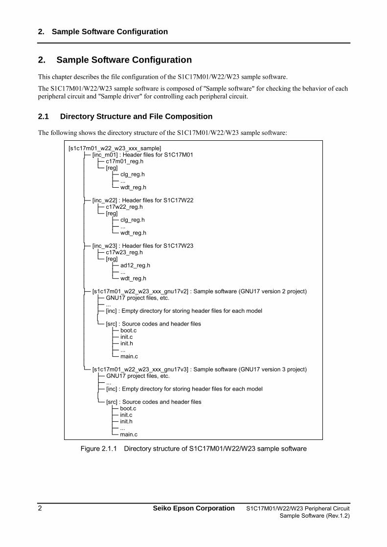
The following shows the directory structure of the S1C17M01/W22/W23 sample software:
Figure 2.1.1 Directory structure of S1C17M01/W22/W23 sample software
[s1c17m01_w22_w23_xxx_sample] ├─ [inc_m01] : Header files for S1C17M01 │ ├─ c17m01_reg.h │ └─ [reg] │ ├─ clg_reg.h │ ├─ ... │ └─ wdt_reg.h │ ├─ [inc_w22] : Header files for S1C17W22 │ ├─ c17w22_reg.h │ └─ [reg] │ ├─ clg_reg.h │ ├─ ... │ └─ wdt_reg.h │ ├─ [inc_w23] : Header files for S1C17W23 │ ├─ c17w23_reg.h │ └─ [reg] │ ├─ ad12_reg.h │ ├─ ... │ └─ wdt_reg.h │ ├─ [s1c17m01_w22_w23_xxx_gnu17v2] : Sample software (GNU17 version 2 project) │ ├─ GNU17 project files, etc. │ ├─ ... │ ├─ [inc] : Empty directory for storing header files for each model │ │ │ └─ [src] : Source codes and header files │ ├─ boot.c │ ├─ init.c │ ├─ init.h │ ├─ ... │ └─ main.c │ └─ [s1c17m01_w22_w23_xxx_gnu17v3] : Sample software (GNU17 version 3 project)
├─ GNU17 project files, etc. ├─ ... ├─ [inc] : Empty directory for storing header files for each model │ └─ [src] : Source codes and header files ├─ boot.c ├─ init.c ├─ init.h ├─ ... └─ main.c

2. Sample Software Configuration
S1C17M01/W22/W23 Peripheral Circuit Seiko Epson Corporation 3 Sample Software (Rev.1.2)
(1) s1c17m01_w22_w23_xxx_sample, s1c17m01_xxx_sample, s1c17w22_w23_xxx_sample, and s1c17w23_xxx_sample directories
These directories contain the sample software.
(2) inc_m01, inc_w22, and inc_w23 directories
These directories contain the header files in which the model dependent information such as the registers of the S1C17M01 and S1C17W22/W23 are defined .
・ Header file which defines the register address and other information of S1C17M01 (c17m01_reg.h) ・ Header file which defines the register address and other information of S1C17W22 (c17w22_reg.h) ・ Header file which defines the register address and other information of S1C17W23 (c17W23_reg.h)
(3) reg directory
This directory contains the header files in which the control bit assignments for each peripheral circuit are defined.
・ Header files which define the control bit assignments for each peripheral circuit (clg_reg.h, etc.)
(4) s1c17m01_w22_w23_xxx_gnu17vx, s1c17m01_xxx_gnu17vx. s1c17w22_w23_xxx_gnu17vx, and s1c17w23_xxx_gnu17vx directories
These directories contain the files which pertain the GNU17 project.
"_gnu17v2" and "_gnu17v3," the last part of the directory names, represent the GNU17 version.
(5) inc directory
This directory is used to place the header files to be used for the project by copying from directories (2) and (3).
(6) src directory
This directory contains microcontroller initialization programs, sample programs and drivers for controlling the peripheral circuits, and the header files in which the constants and other items used in the sample programs and drivers are defined.
・ File that contains vector table and initialization processing (boot.c) ・ Sample software file for each peripheral circuit (main.c) ・ Sample driver files for each peripheral circuit (init.c, clg.c, etc.) ・ Sample driver header files for each peripheral circuit (init.h, clg.h, etc.)

3. Execution Method
4 Seiko Epson Corporation S1C17M01/W22/W23 Peripheral Circuit Sample Software (Rev.1.2)
3. Execution Method
3.1 Software Development Environment
This chapter describes the software development environment using the following tools. For more information on each tool, refer to each tool manual.
・ S5U1C17001C (GNU17) ver. 2.3.0/ver. 3.05 ・ Model information files (S1C17M01, S1C17W22, S1C17W23) ・ S5U1C17001H (ICDmini) ver. 2.0/ver. 3.0 3.2 Installing each Tool
(1) GNU17 version 2/version 3 (S5U1C17001C)
・ Download the compressed GNU17 file from the Epson MCU users site. https://www.epsondevice.com/support_e/mcu/product/c17.html
・ Decompress the compressed GNU17 file into any folder. ・ Run Setup.exe to install GNU17.
(2) Install the model information files
・ Confirm and download the latest model information files from the Epson MCU users site. https://www.epsondevice.com/support_e/mcu/product/page04.html#02
・ Decompress the downloaded model information files into the [mcu_model] subfolder of the folder where GNU17 is installed. Example: When the S1C17M01 model information files are added
Figure 3.2.1 Adding model information files for S1C17M01
(3) ICDmini ver. 2.0 (S5U1C17001H)
・ After installing GNU17 version 2, connect between the ICDmini and the PC with the USB cable. ・ Install the USB driver, that exists in the folder where the GNU17 was installed, to the PC. When the
GNU17 was installed in the C:\EPSON\GNU17 directory, the USB driver was placed into the directories shown below. For 32-bit OS: C:\EPSON\GNU17\utility\drv_usb\OS_32bit For 64-bit OS: C:\EPSON\GNU17\utility\drv_usb\OS_64bit
(4) ICDmini ver. 3.0 (S5U1C17001H)
・ After installing GNU17 version 3, connect between the ICDmini and the PC with the USB cable. ・ Install the USB driver, that exists in the folder where the GNU17 was installed, to the PC. When the
GNU17 was installed in the C:\EPSON\GNU17V3 directory, the USB driver was placed into the C:\EPSON\GNU17V3\utility\drv_usb\Mini3Driver directory.
[GNU17] ├─ [mcu_model] : Model information folder │ ├─ [17xxx] │ ├─ ... │ └─ [17M01] │ ├─ S1C17M01.ini │ ├─ S1C17M01.properties │ ├─ ... │ └─ [fls] │ ├─ fls17M01_readme_j.txt │ ├─ ... │ └─ fls17M01.elf ├─ ...
Added
model
information files
for each model
3. Execution Method
S1C17M01/W22/W23 Peripheral Circuit Seiko Epson Corporation 5 Sample Software (Rev.1.2)
3.3 Importing Project
This section describes how to import the sample program into GNU17.
Notes: • For more information on importing programs, refer to the S5U1C17001C Manual.
• The program import procedure between GNU17 version 2 and version 3 is different.
3.3.1 Importing Sample Program (Common to GNU17 version 2 and version 3)
(1) Launch GNU17 IDE
Double-click the eclipse.exe icon in the eclipse sub-directory of the directory where GNU17 was installed to launch IDE. IDE is also launched by selecting [EPSON MCU] > [GNU17] > [GNU17 IDE] ([EPSON MCU] >[GNU17V3] > [GNU17V3 IDE] in GNU17 version 3) from the Windows startup menu.
(2) Decompress sample program
Decompress the sample program downloaded from the Epson MCU users site.
(3) Copy the header files for each model
Copy the header files for each model to the sample software's project folder.
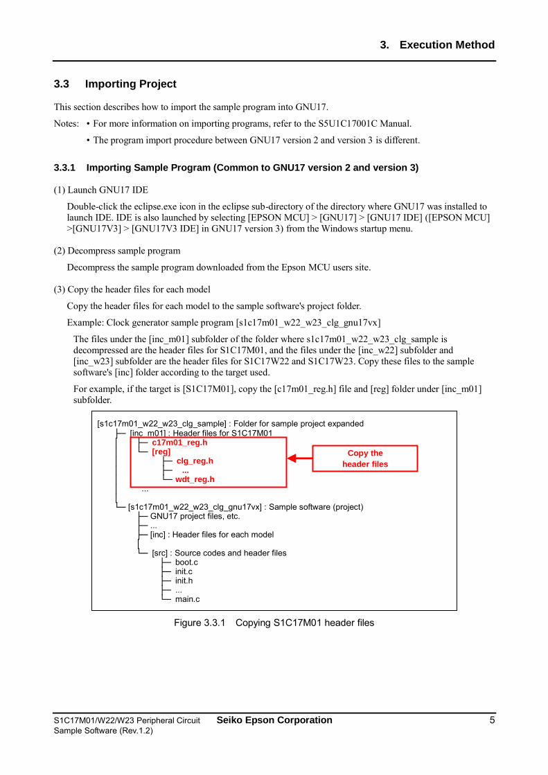
Example: Clock generator sample program [s1c17m01_w22_w23_clg_gnu17vx]
The files under the [inc_m01] subfolder of the folder where s1c17m01_w22_w23_clg_sample is decompressed are the header files for S1C17M01, and the files under the [inc_w22] subfolder and [inc_w23] subfolder are the header files for S1C17W22 and S1C17W23. Copy these files to the sample software's [inc] folder according to the target used.
For example, if the target is [S1C17M01], copy the [c17m01_reg.h] file and [reg] folder under [inc_m01] subfolder.
Figure 3.3.1 Copying S1C17M01 header files
[s1c17m01_w22_w23_clg_sample] : Folder for sample project expanded ├─ [inc_m01] : Header files for S1C17M01 │ ├─ c17m01_reg.h │ └─ [reg] │ ├─ clg_reg.h │ ├─ ... │ └─ wdt_reg.h │ ... │ └─ [s1c17m01_w22_w23_clg_gnu17vx] : Sample software (project)
├─ GNU17 project files, etc. ├─ ... ├─ [inc] : Header files for each model │ └─ [src] : Source codes and header files ├─ boot.c ├─ init.c ├─ init.h ├─ ... └─ main.c
Copy the
header files

3. Execution Method
6 Seiko Epson Corporation S1C17M01/W22/W23 Peripheral Circuit Sample Software (Rev.1.2)
Place the copied header files into [inc] subfolder in the sample software's [s1c17m01_w22_w23_clg_gnu17vx] folder, as shown below:
Figure 3.3.2 Pasting S1C17M01 header files
(4) Editing the header file
Edit the sample software header file [inc\init.h] according to the target CPU. Uncomment the #include line for the target CPU written under [// MCU select].
Example: When using the S1C17M01 sample software
// MCU select
#include MCUSEL_C17M01
//#include MCUSEL_C17W22
//#include MCUSEL_C17W23
Example: When using the S1C17W22 sample software
// MCU select
//#include MCUSEL_C17M01
#include MCUSEL_C17W22
//#include MCUSEL_C17W23
[s1c17m01_w22_w23_clg_sample] : Folder for sample project expanded ├─ [inc_m01] : Header files for S1C17M01 ├─ [inc_w22] : Header files for S1C17W22 │ ... │ └─ [s1c17m01_w22_w23_clg_gnu17vx] : Sample software (project)
├─ GNU17 project files, etc. ├─ ... ├─ [inc] : Header files for each model │ ├─ c17m01_reg.h │ └─ [reg] │ ├─ clg_reg.h │ ├─ ... │ └─ wdt_reg.h │ └─ [src] : Source codes and header files ├─ boot.c ├─ init.c ├─ init.h ├─ ... └─ main.c
Paste the
header files
3. Execution Method
S1C17M01/W22/W23 Peripheral Circuit Seiko Epson Corporation 7 Sample Software (Rev.1.2)
3.3.2 Importing Sample Program (GNU17 version 2)
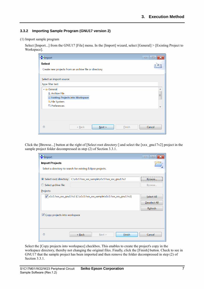
(1) Import sample program
Select [Import...] from the GNU17 [File] menu. In the [Import] wizard, select [General] > [Existing Project to Workspace].
Click the [Browse...] button at the right of [Select root directory:] and select the [xxx_gnu17v2] project in the sample project folder decompressed in step (2) of Section 3.3.1.
Select the [Copy projects into workspace] checkbox. This enables to create the project's copy in the workspace directory, thereby not changing the original files. Finally, click the [Finish] button. Check to see in GNU17 that the sample project has been imported and then remove the folder decompressed in step (2) of Section 3.3.1.
3. Execution Method
8 Seiko Epson Corporation S1C17M01/W22/W23 Peripheral Circuit Sample Software (Rev.1.2)
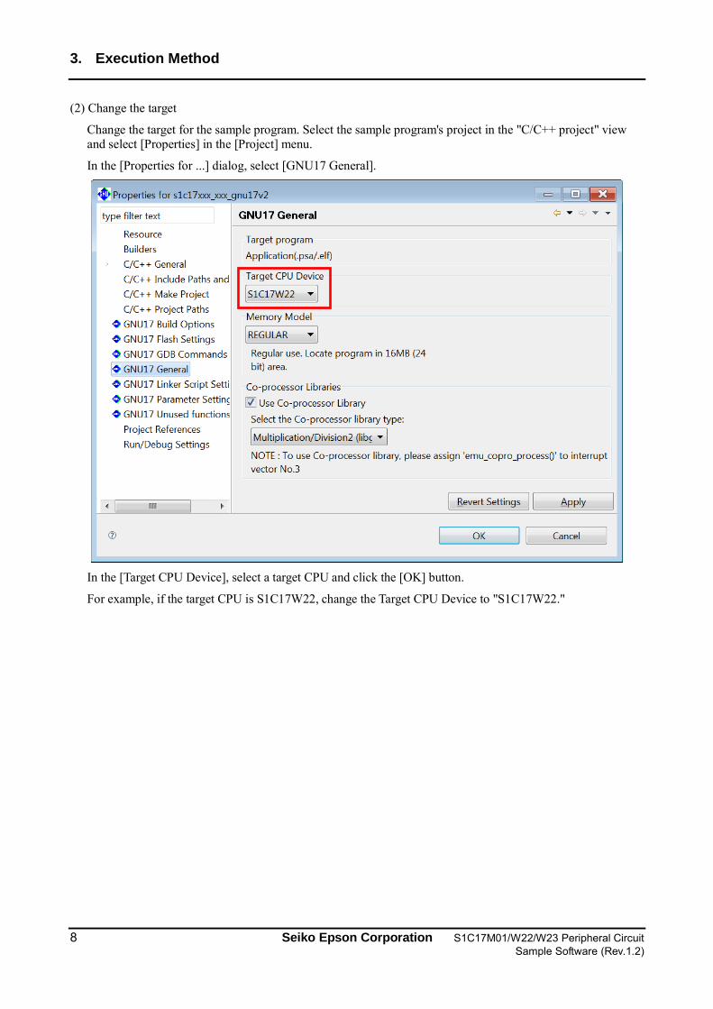
(2) Change the target
Change the target for the sample program. Select the sample program's project in the "C/C++ project" view and select [Properties] in the [Project] menu.
In the [Properties for ...] dialog, select [GNU17 General].
In the [Target CPU Device], select a target CPU and click the [OK] button.
For example, if the target CPU is S1C17W22, change the Target CPU Device to "S1C17W22."
3. Execution Method
S1C17M01/W22/W23 Peripheral Circuit Seiko Epson Corporation 9 Sample Software (Rev.1.2)
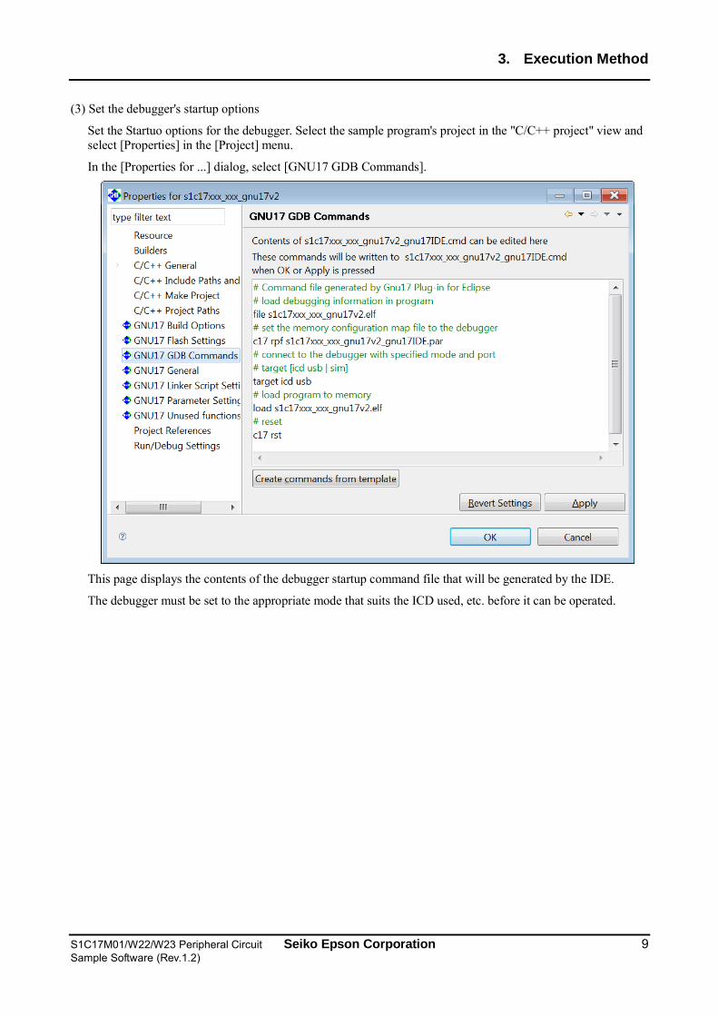
(3) Set the debugger's startup options
Set the Startuo options for the debugger. Select the sample program's project in the "C/C++ project" view and select [Properties] in the [Project] menu.
In the [Properties for ...] dialog, select [GNU17 GDB Commands].
This page displays the contents of the debugger startup command file that will be generated by the IDE.
The debugger must be set to the appropriate mode that suits the ICD used, etc. before it can be operated.
3. Execution Method
10 Seiko Epson Corporation S1C17M01/W22/W23 Peripheral Circuit Sample Software (Rev.1.2)
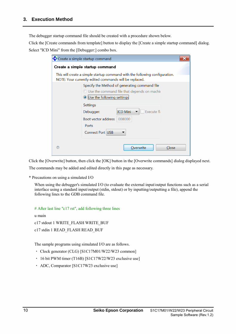
The debugger startup command file should be created with a procedure shown below.
Click the [Create commands from template] button to display the [Create a simple startup command] dialog.
Select "ICD Mini" from the [Debugger:] combo box.
Click the [Overwrite] button, then click the [OK] button in the [Overwrite commands] dialog displayed next.
The commands may be added and edited directly in this page as necessary.
* Precautions on using a simulated I/O
When using the debugger's simulated I/O (to evaluate the external input/output functions such as a serial interface using a standard input/output (stdin, stdout) or by inputting/outputting a file), append the following lines to the GDB command file.
# After last line "c17 rst", add following three lines
u main
c17 stdout 1 WRITE_FLASH WRITE_BUF
c17 stdin 1 READ_FLASH READ_BUF
The sample programs using simulated I/O are as follows.
・ Clock generator (CLG) [S1C17M01/W22/W23 common]
・ 16 bit PWM timer (T16B) [S1C17W22/W23 exclusive use]
・ ADC, Comparator [S1C17W23 exclusive use]
3. Execution Method
S1C17M01/W22/W23 Peripheral Circuit Seiko Epson Corporation 11 Sample Software (Rev.1.2)
3.3.3 Importing Sample Program (GNU17 version 3)
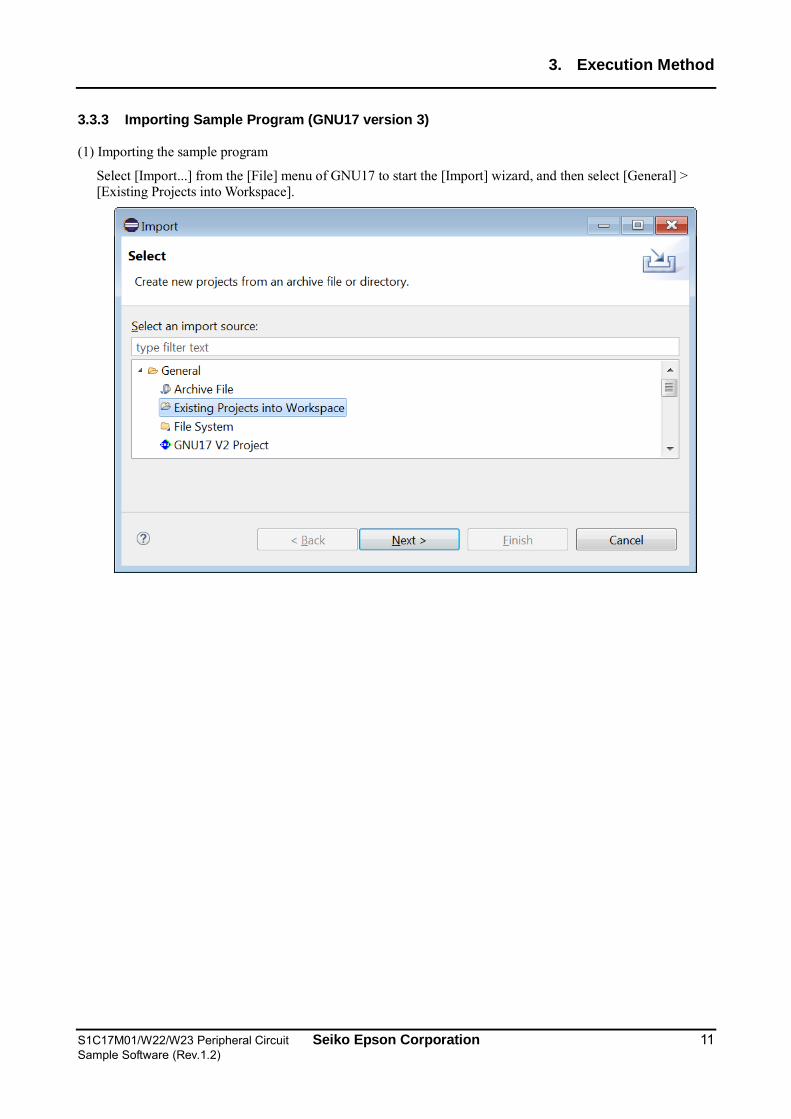
(1) Importing the sample program
Select [Import...] from the [File] menu of GNU17 to start the [Import] wizard, and then select [General] > [Existing Projects into Workspace].
3. Execution Method
12 Seiko Epson Corporation S1C17M01/W22/W23 Peripheral Circuit Sample Software (Rev.1.2)
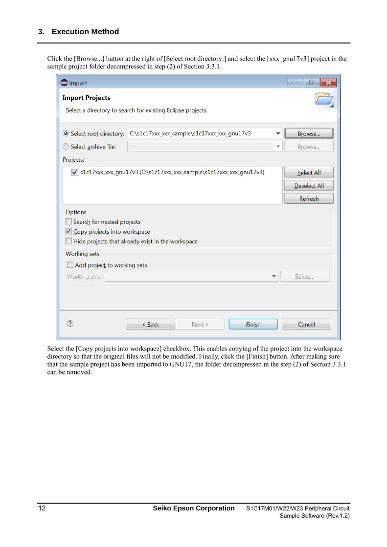
Click the [Browse...] button at the right of [Select root directory:] and select the [xxx_gnu17v3] project in the sample project folder decompressed in step (2) of Section 3.3.1.
Select the [Copy projects into workspace] checkbox. This enables copying of the project into the workspace directory so that the original files will not be modified. Finally, click the [Finish] button. After making sure that the sample project has been imported to GNU17, the folder decompressed in the step (2) of Section 3.3.1 can be removed.
3. Execution Method
S1C17M01/W22/W23 Peripheral Circuit Seiko Epson Corporation 13 Sample Software (Rev.1.2)
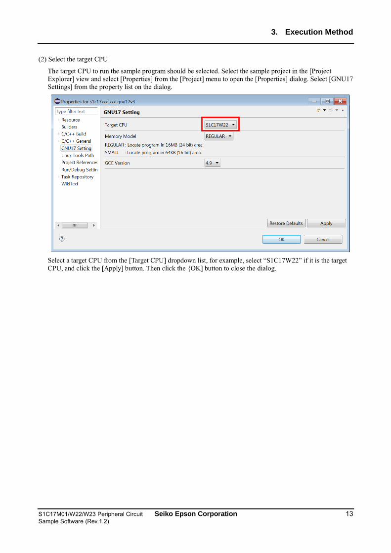
(2) Select the target CPU
The target CPU to run the sample program should be selected. Select the sample project in the [Project Explorer] view and select [Properties] from the [Project] menu to open the [Properties] dialog. Select [GNU17 Settings] from the property list on the dialog.
Select a target CPU from the [Target CPU] dropdown list, for example, select “S1C17W22” if it is the target CPU, and click the [Apply] button. Then click the {OK] button to close the dialog.

3. Execution Method
14 Seiko Epson Corporation S1C17M01/W22/W23 Peripheral Circuit Sample Software (Rev.1.2)
(3) Setting the debugger startup options
The debugger startup options should be selected. Expand the sample project in the [Project Explorer] view and open [gdbmini3.ini] with the editor.
The editor displays the contents of the debugger startup command file. The debugger must be set to the appropriate mode that suits the microcontroller and ICD used.
* Precautions on using the standard output
When using the standard output, uncomment (remove #) the command lines of the GDB command file as shown below (the lines highlighted in red) to enable them to be executed.
GDB command file [gdbmini3.ini]
# Please uncomment following commented out lines to enable STDOUT while debugging. hb WRITE_FLASH commands printf "%s",WRITE_BUF c end
The following sample programs use the standard output:
・ Clock generator (CLG) [Common to S1C17M01/W22/W23]
・ 16-bit PWM timer (T16B) [Only for S1C17W22/W23]
・ ADC, Comparator [Only for S1C17W23]
3. Execution Method
S1C17M01/W22/W23 Peripheral Circuit Seiko Epson Corporation 15 Sample Software (Rev.1.2)
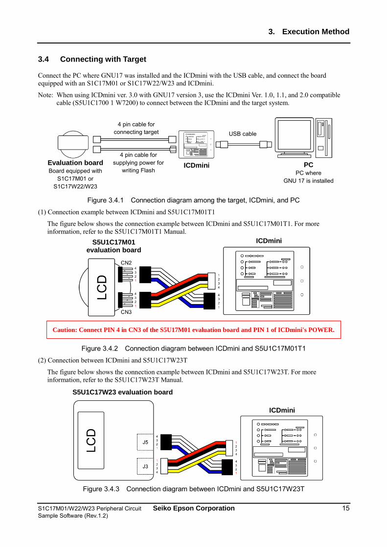
3.4 Connecting with Target
Connect the PC where GNU17 was installed and the ICDmini with the USB cable, and connect the board equipped with an S1C17M01 or S1C17W22/W23 and ICDmini.
Note: When using ICDmini ver. 3.0 with GNU17 version 3, use the ICDmini Ver. 1.0, 1.1, and 2.0 compatible cable (S5U1C17001W7200) to connect between the ICDmini and the target system.
Figure 3.4.1 Connection diagram among the target, ICDmini, and PC
(1) Connection example between ICDmini and S5U1C17M01T1
The figure below shows the connection example between ICDmini and S5U1C17M01T1. For more information, refer to the S5U1C17M01T1 Manual.
Figure 3.4.2 Connection diagram between ICDmini and S5U1C17M01T1
(2) Connection between ICDmini and S5U1C17W23T
The figure below shows the connection example between ICDmini and S5U1C17W23T. For more information, refer to the S5U1C17W23T Manual.
Figure 3.4.3 Connection diagram between ICDmini and S5U1C17W23T
PC PC where
GNU 17 is installed
Evaluation board Board equipped with
S1C17M01 or S1C17W22/W23
4 pin cable for connecting target
4 pin cable for supplying power for
writing Flash
USB cable
ICDmini
ICDmini S5U1C17M01 evaluation board
Caution: Connect PIN 4 in CN3 of the S5U17M01 evaluation board and PIN 1 of ICDmini's POWER.
S5U1C17W23 evaluation board
ICDmini
3. Execution Method
16 Seiko Epson Corporation S1C17M01/W22/W23 Peripheral Circuit Sample Software (Rev.1.2)
3.5 Operating ICDmini and Target
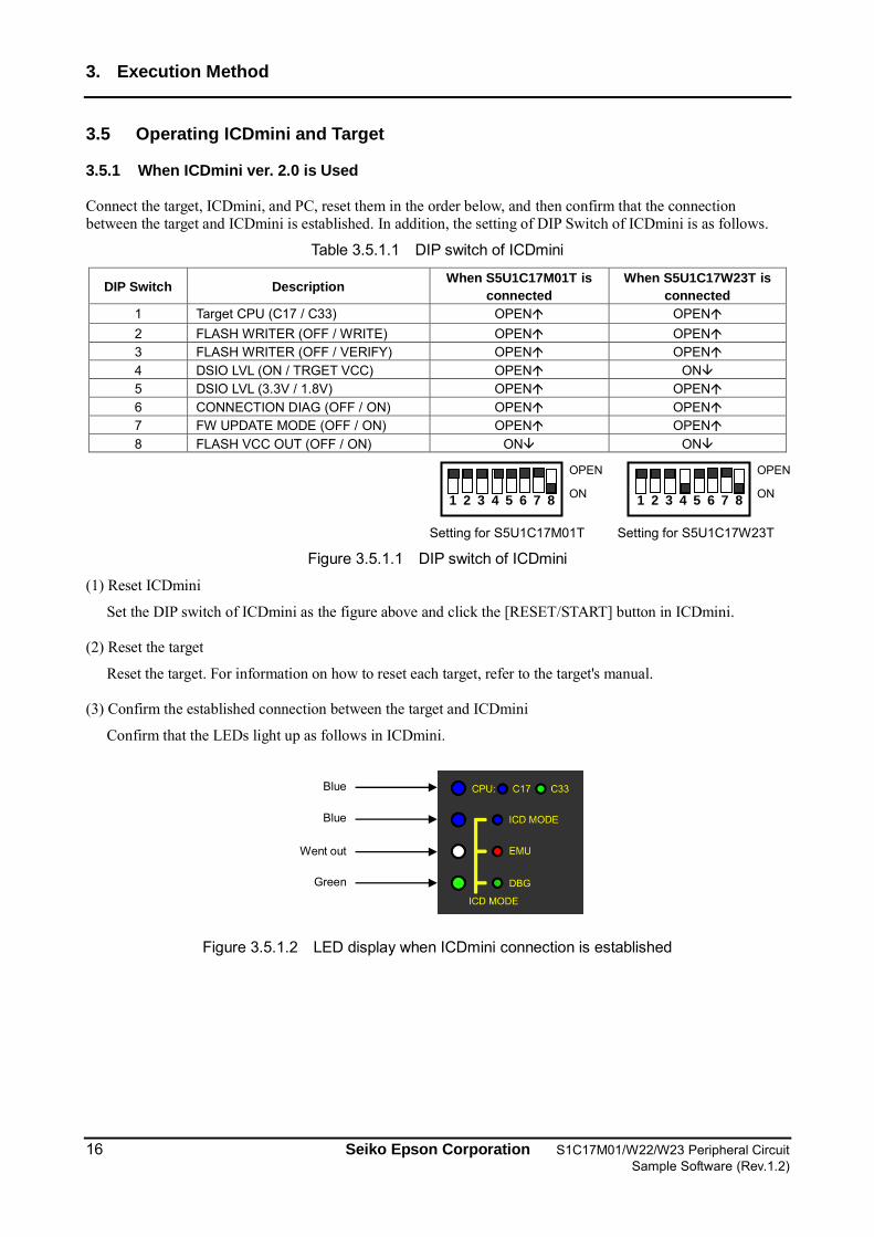
3.5.1 When ICDmini ver. 2.0 is Used
Connect the target, ICDmini, and PC, reset them in the order below, and then confirm that the connection between the target and ICDmini is established. In addition, the setting of DIP Switch of ICDmini is as follows.
Table 3.5.1.1 DIP switch of ICDmini
DIP Switch Description When S5U1C17M01T is
connected
When S5U1C17W23T is
connected
1 Target CPU (C17 / C33) OPEN OPEN 2 FLASH WRITER (OFF / WRITE) OPEN OPEN 3 FLASH WRITER (OFF / VERIFY) OPEN OPEN 4 DSIO LVL (ON / TRGET VCC) OPEN ON 5 DSIO LVL (3.3V / 1.8V) OPEN OPEN 6 CONNECTION DIAG (OFF / ON) OPEN OPEN 7 FW UPDATE MODE (OFF / ON) OPEN OPEN 8 FLASH VCC OUT (OFF / ON) ON ON
Setting for S5U1C17M01T Setting for S5U1C17W23T
Figure 3.5.1.1 DIP switch of ICDmini
(1) Reset ICDmini
Set the DIP switch of ICDmini as the figure above and click the [RESET/START] button in ICDmini.
(2) Reset the target
Reset the target. For information on how to reset each target, refer to the target's manual.
(3) Confirm the established connection between the target and ICDmini
Confirm that the LEDs light up as follows in ICDmini.
Figure 3.5.1.2 LED display when ICDmini connection is established
Blue
Blue
Went out
Green
1 2 3 4 5 6 7 8
OPEN ON 1 2 3 4 5 6 7 8
OPEN ON
3. Execution Method
S1C17M01/W22/W23 Peripheral Circuit Seiko Epson Corporation 17 Sample Software (Rev.1.2)
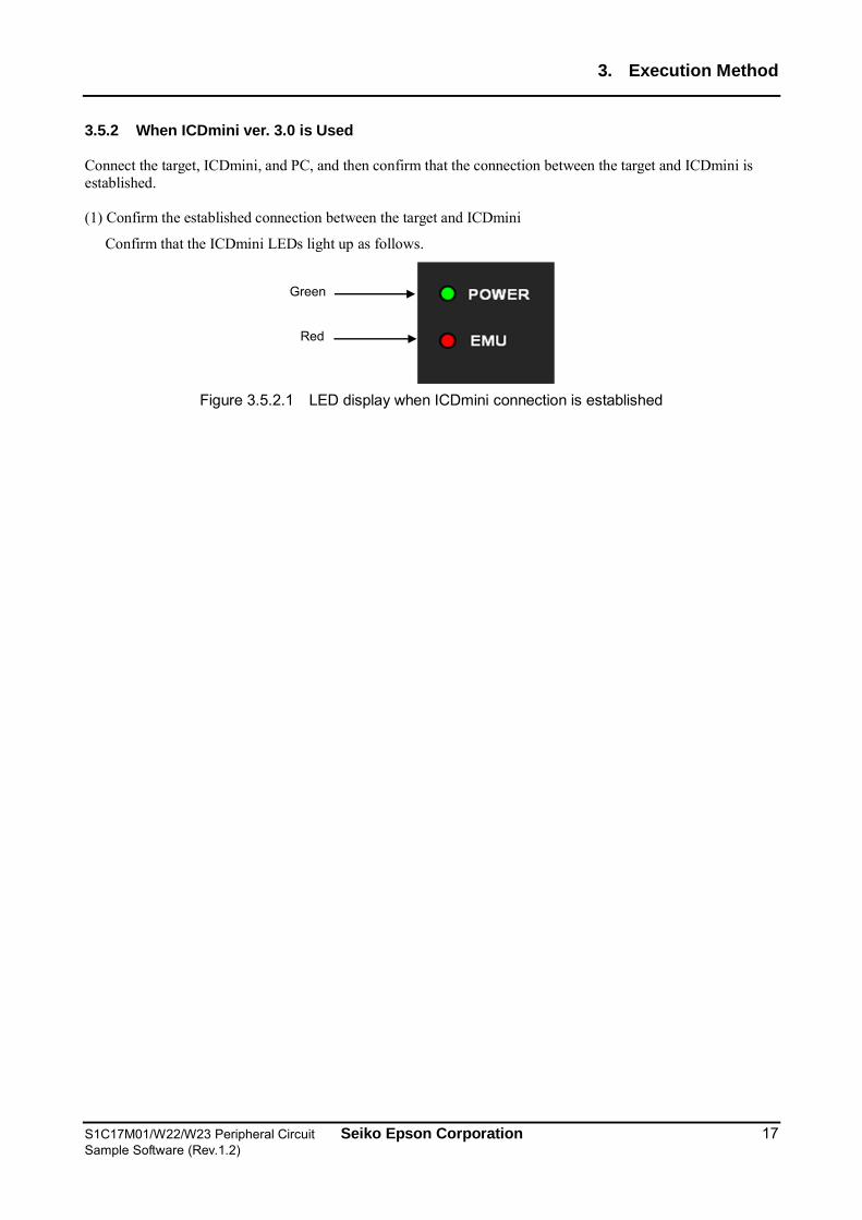
3.5.2 When ICDmini ver. 3.0 is Used
Connect the target, ICDmini, and PC, and then confirm that the connection between the target and ICDmini is established.
(1) Confirm the established connection between the target and ICDmini
Confirm that the ICDmini LEDs light up as follows.
Figure 3.5.2.1 LED display when ICDmini connection is established
Green
Red
3. Execution Method
18 Seiko Epson Corporation S1C17M01/W22/W23 Peripheral Circuit Sample Software (Rev.1.2)
3.6 Building Project and Starting Debugger
This section describes how to build the sample program and start the debugger.
Notes: • For more information on how to build and start the debugger, refer to the S5U1C17001C Manual.
• Be aware that the IC may not operate normally if you terminate the program that is controlling the clocks or the related functions. For debugging the codes concerned, refer to the DCLK change mode command described in the S5U1C17001C Manual.
3.6.1 When GNU17 version 2 is Used
(1) Build programs
In the GNU17's "C/C++ project" view, select the desired project to build. In the GNU17's [Project] menu, select [Build Project] to build the project. Select the desired project in the GNU17's "C/C++ project" view and select [Project's Build] in the context menu displayed by right-clicking the project to also build the project.
(2) Display debugger launch configuration dialog
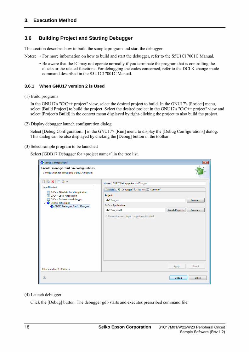
Select [Debug Configuration...] in the GNU17's [Run] menu to display the [Debug Configurations] dialog. This dialog can be also displayed by clicking the [Debug] button in the toolbar.
(3) Select sample program to be launched
Select [GDB17 Debugger for <project name>] in the tree list.
(4) Launch debugger
Click the [Debug] button. The debugger gdb starts and executes prescribed command file.

3. Execution Method
S1C17M01/W22/W23 Peripheral Circuit Seiko Epson Corporation 19 Sample Software (Rev.1.2)
3.6.2 When GNU17 version 3 is Used
(1) Building
In the [Project Explorer] view, select the project to be built. Select [Build Project] from the [Project] menu (or the context menu that appears by right-clicking the project) to execute building.
(2) Displaying [Debug Configuration] dialog
Select [Debug Configurations...] from the GNU17 [Run] menu or the [Debug] dropdown list on the toolbar to display the [Debug Configurations] dialog.
(3) Configuring the debugger
Open the [Debugger] tab page and specify [gdbmini3.ini] for [GDB command file:]. ([gdbmini3.ini] has been specified by default in the sample project.) Click the [Apply] button and then the [Debug] button to execute the specified command file.
4. Details of Sample Software Function
20 Seiko Epson Corporation S1C17M01/W22/W23 Peripheral Circuit Sample Software (Rev.1.2)
4. Details of Sample Software Function
This chapter describes the functions of the S1C17M01/W22/W23 sample software in detail.
4.1 I/O Port (P) [Common to S1C17M01/W22/W23]
4.1.1 Sample Software Specification
This sample software works as follows by using I/O ports.
• When a port is set to input and the input signal becomes High or Low level, an interrupt occurs. • The port is set to output and a High or Low level signal is output.
The table below lists the ports to be used and port names.
Table 4.1.1 I/O port setting list
Setting Port name
Input interrupt port P01 Output port P02
4.1.2 Hardware Conditions
This sample program runs in the OSC1 built-in oscillating circuit (32.768kHz) in the microcontroller.
For this sample program, connect the ports as follows in the microcontroller.
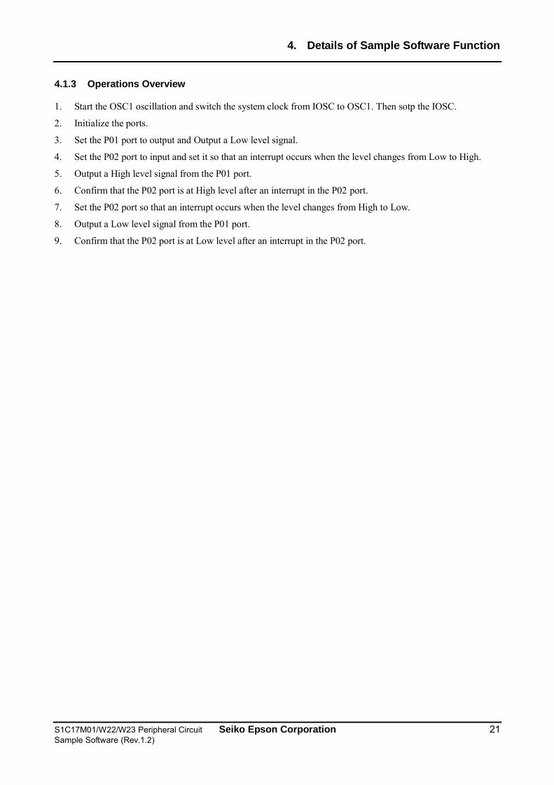
Figure 4.1.1 I/O port (P) sample software/hardware connection diagram
S1C17M01 or S1C17W22/W23 evaluation board
P01
P02
4. Details of Sample Software Function
S1C17M01/W22/W23 Peripheral Circuit Seiko Epson Corporation 21 Sample Software (Rev.1.2)
4.1.3 Operations Overview
1. Start the OSC1 oscillation and switch the system clock from IOSC to OSC1. Then sotp the IOSC.
2. Initialize the ports.
3. Set the P01 port to output and Output a Low level signal.
4. Set the P02 port to input and set it so that an interrupt occurs when the level changes from Low to High.
5. Output a High level signal from the P01 port.
6. Confirm that the P02 port is at High level after an interrupt in the P02 port.
7. Set the P02 port so that an interrupt occurs when the level changes from High to Low.
8. Output a Low level signal from the P01 port.
9. Confirm that the P02 port is at Low level after an interrupt in the P02 port.

4. Details of Sample Software Function
22 Seiko Epson Corporation S1C17M01/W22/W23 Peripheral Circuit Sample Software (Rev.1.2)
4.2 Clock Generator (CLG) [Common to S1C17M01/W22/W23]
4.2.1 Sample Software Specification
This sample program works as follows by using OSC.
• Oscillate and stop OSC1. • Oscillate and stop OSC3 (S1C17W22/W23 only). The setting of the oscillatory frequency is possible, too. • Oscillate and stop IOSC. • Change the system clock to OSC1. • Change the system clock to OSC3. • Change the system clock to IOSC. • In the case of system clock is IOSC (S1C17M01/W22/W23) / OSC3 (only for S1C17W22/W23), do the
transition control between SLEEP mode and RUN mode. • Do the transition control between OSC1 HALT, IOSC RUN (S1C17M01/W22/W23, and OSC3 RUN (only for
S1C17W22/W23). • Change the system clock of OSC3 (only for S1C17W22/W23) 4.2.2 Hardware Conditions
This sample program works by using the built-in oscillation (IOSC) in the microcontroller. Then change the system clock to OSC1 or OSC3 (only S1C17W22/W23). Therefore it needs transducer. For details, please refer to "Clock Generator (CLG)" in S1C17M01/S1C17W22/W23 technical manual.
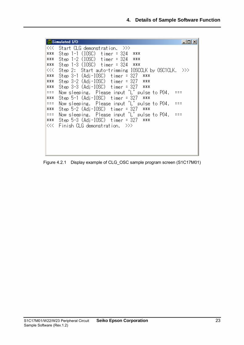
4.2.3 Operations Overview (S1C17M01)
This sample program starts to work while IOSC is working.
This sample program starts to work by using IOSC as a system clock. Note that the count value displayed below is estimated to be a little bigger than 327, the 10 millisecond count value of OSC1's oscillating frequency = 32.768kHz. 0. Start to oscillate OSC1, change the system clock to OSC1, and then stop the IOSC oscillation. 1. Stop CPU (HALT) and repeat to interrupt the timer three times per second. Each time a timer interrupt is
received, start the IOSC oscillation, execute 10 milliseconds of loop, display a difference between the T16 timer count values before and after the loop on Simulated I/O, and stop IOSC.
2. Trim IOSC's oscillating frequency automatically based on the OSC1's oscillating clock. 3. Since this operation is the same as step 1, the automatic trimming result can be confirmed. 4. This step does nothing. This step is added only from a compatibility point of view with S1C17W22/W23's
behavior. 5. After IOSC started to oscillate, stop CPU (SLEEP). In order to wake up CPU from the sleep mode, it is
necessary to put the level "L" signal into port P04. When CPU wakes up and IOSC automatically starts to oscillate, execute 10 milliseconds of loop, display a difference between the T16 timer count values before and after the loop on Simulated I/O, and stop IOSC. This operation is repeated three times.
Finally, the program starts the IOSC oscillation, stops the OSC1 and OSC3 oscillations to finish the series of operations.
4. Details of Sample Software Function
S1C17M01/W22/W23 Peripheral Circuit Seiko Epson Corporation 23 Sample Software (Rev.1.2)
Figure 4.2.1 Display example of CLG_OSC sample program screen (S1C17M01)
4. Details of Sample Software Function
24 Seiko Epson Corporation S1C17M01/W22/W23 Peripheral Circuit Sample Software (Rev.1.2)
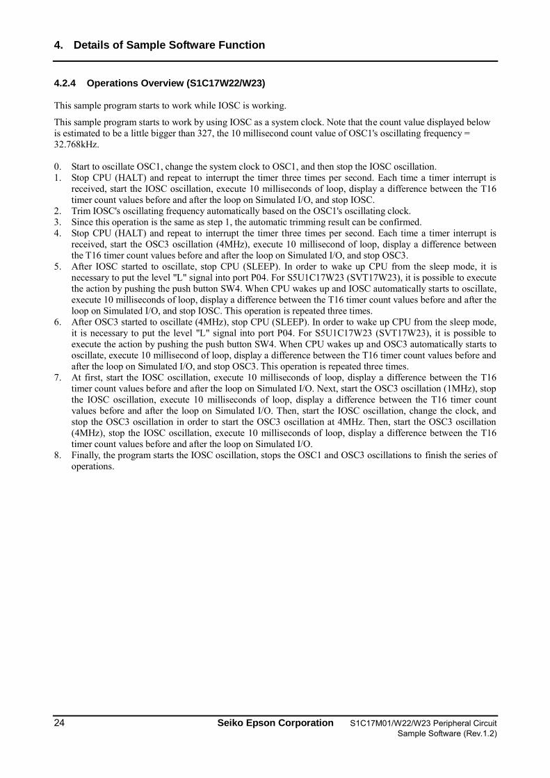
4.2.4 Operations Overview (S1C17W22/W23)
This sample program starts to work while IOSC is working.
This sample program starts to work by using IOSC as a system clock. Note that the count value displayed below is estimated to be a little bigger than 327, the 10 millisecond count value of OSC1's oscillating frequency = 32.768kHz. 0. Start to oscillate OSC1, change the system clock to OSC1, and then stop the IOSC oscillation. 1. Stop CPU (HALT) and repeat to interrupt the timer three times per second. Each time a timer interrupt is
received, start the IOSC oscillation, execute 10 milliseconds of loop, display a difference between the T16 timer count values before and after the loop on Simulated I/O, and stop IOSC.
2. Trim IOSC's oscillating frequency automatically based on the OSC1's oscillating clock. 3. Since this operation is the same as step 1, the automatic trimming result can be confirmed. 4. Stop CPU (HALT) and repeat to interrupt the timer three times per second. Each time a timer interrupt is
received, start the OSC3 oscillation (4MHz), execute 10 millisecond of loop, display a difference between the T16 timer count values before and after the loop on Simulated I/O, and stop OSC3.
5. After IOSC started to oscillate, stop CPU (SLEEP). In order to wake up CPU from the sleep mode, it is necessary to put the level "L" signal into port P04. For S5U1C17W23 (SVT17W23), it is possible to execute the action by pushing the push button SW4. When CPU wakes up and IOSC automatically starts to oscillate, execute 10 milliseconds of loop, display a difference between the T16 timer count values before and after the loop on Simulated I/O, and stop IOSC. This operation is repeated three times.
6. After OSC3 started to oscillate (4MHz), stop CPU (SLEEP). In order to wake up CPU from the sleep mode, it is necessary to put the level "L" signal into port P04. For S5U1C17W23 (SVT17W23), it is possible to execute the action by pushing the push button SW4. When CPU wakes up and OSC3 automatically starts to oscillate, execute 10 millisecond of loop, display a difference between the T16 timer count values before and after the loop on Simulated I/O, and stop OSC3. This operation is repeated three times.
7. At first, start the IOSC oscillation, execute 10 milliseconds of loop, display a difference between the T16 timer count values before and after the loop on Simulated I/O. Next, start the OSC3 oscillation (1MHz), stop the IOSC oscillation, execute 10 milliseconds of loop, display a difference between the T16 timer count values before and after the loop on Simulated I/O. Then, start the IOSC oscillation, change the clock, and stop the OSC3 oscillation in order to start the OSC3 oscillation at 4MHz. Then, start the OSC3 oscillation (4MHz), stop the IOSC oscillation, execute 10 milliseconds of loop, display a difference between the T16 timer count values before and after the loop on Simulated I/O.
8. Finally, the program starts the IOSC oscillation, stops the OSC1 and OSC3 oscillations to finish the series of operations.
4. Details of Sample Software Function
S1C17M01/W22/W23 Peripheral Circuit Seiko Epson Corporation 25 Sample Software (Rev.1.2)
Figure 4.2.2 Display example of CLG_OSC sample program screen (S1C17W22/W23)
4. Details of Sample Software Function
26 Seiko Epson Corporation S1C17M01/W22/W23 Peripheral Circuit Sample Software (Rev.1.2)
4.3 16-Bit Timer (T16) [Common to S1C17M01/W22/W23]
4.3.1 Sample Software Specification
The 16-bit timer sample program works as follows by using 16-bit timer.
• Cause an interrupt in the 16-bit timer to get a counter value of the timer. • When waiting for an interrupt, put CPU in a halt mode to reduce the power consumption. 4.3.2 Hardware Conditions
This sample program runs in the IOSC built-in oscillating circuit in the microcontroller.
• S1C17M01: 7.37MHz • S1C17W22/W23: 700kHz 4.3.3 Operations Overview
1. Set the counter of the 16-bit timer.
2. Start the 16-bit timer and put CPU in a Halt state.
3. When an interrupt occurs in the 16-bit timer, release CPU from the Halt state.
4. Get the number of interrupts of the 16-bit timer.
5. When the number of interrupts of the 16-bit timer is less than 1000, put CPU in a Halt state again.
6. When the number of interrupts of the 16-bit timer is not less than 1000, stop the 16-bit timer and exit the sample program.
4. Details of Sample Software Function
S1C17M01/W22/W23 Peripheral Circuit Seiko Epson Corporation 27 Sample Software (Rev.1.2)
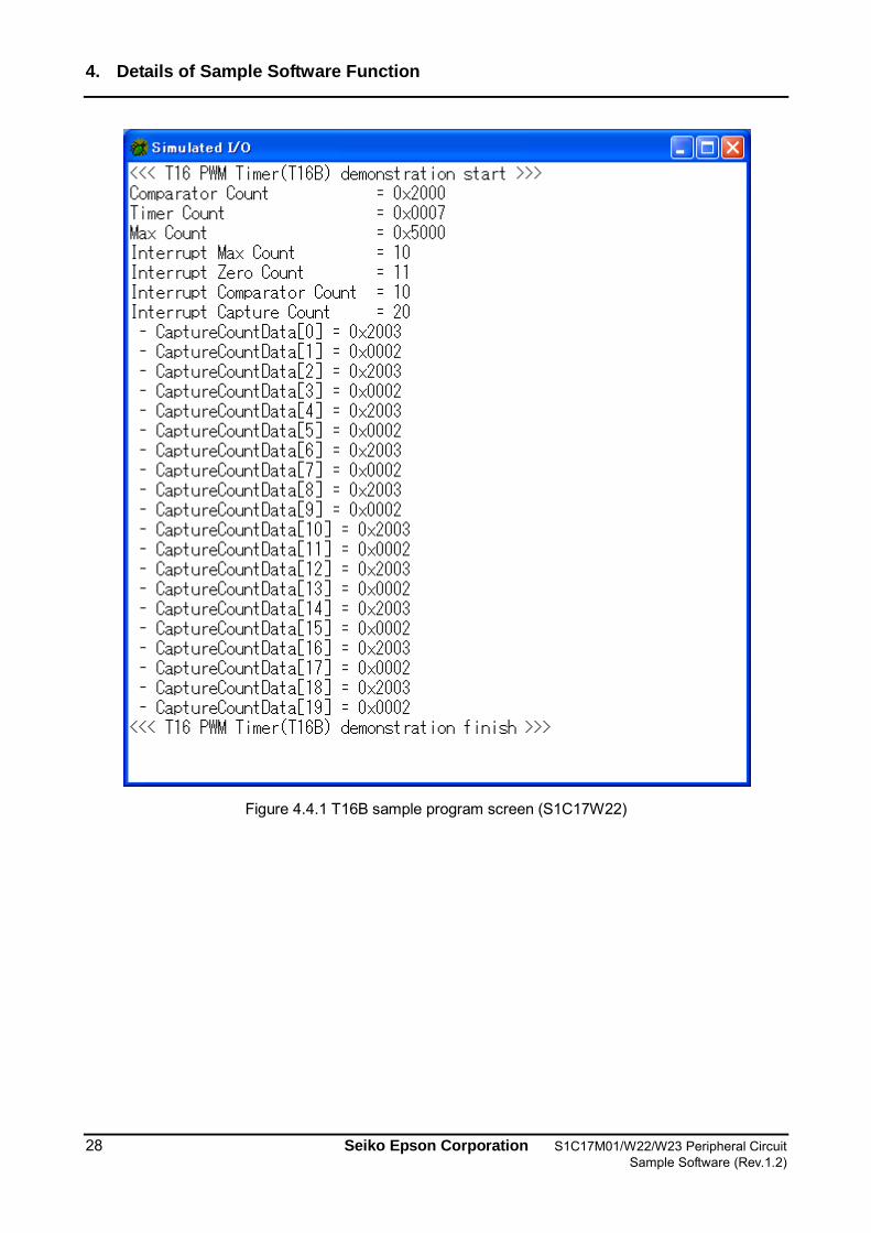
4.4 16-Bit PWM Timer (T16B) [Only for S1C17W22/W23]
4.4.1 Sample Software Specification
The 16-bit PWM timer sample program works as follows by using 16-bit PWM timer.
• Cause a comparator interrupt in the 16-bit PWM timer. • Cause a capture interrupt in the 16-bit PWM timer to get a counter value of the timer. • When waiting for an interrupt, put CPU in a halt mode to reduce the power consumption. 4.4.2 Hardware Conditions
This sample program runs in the IOSC built-in oscillating circuit in the microcontroller.
• S1C17W22/W23: 700kHz 4.4.3 Operations Overview
1. Set the 16bit PWM timer as follows and start the T16-bit PWM timer.
• Mode: Repeat up-count mode • Maximum counter value: 0x5000 • Comparator/capture circuit 0: Comparator mode (compare buffer: 0x2000) • Comparator/capture circuit 1: Number of capture interrupts in capture mode (trigger signal: LOW)
2. Start the 16-bit PWM timer and put CPU in a Halt state.
3. When an interrupt occurs in the 16-bit PWM timer, release CPU from the Halt state.
4. Each time an interrupt occurs in the 16-bit PWM timer, get the number of interrupts below:
• Number of compare interrupts • Number of capture interrupts • Number of maximum-count interrupts • Number of count-zero interrupts
5. When a compare interrupt occurs, set the trigger signal for capture to HIGH.
6. When a maximum-count interrupt occurs, set the trigger signal for capture to LOW.
7. When the number of maximum-count interrupts is less than 10, put CPU in a Halt state again.
8. When the number of maximum-count interrupts is not less than 10, stop the 16-bit timer, shows a count value when an interrupt occurred for Simulated I/O and exit the sample program.
4. Details of Sample Software Function
28 Seiko Epson Corporation S1C17M01/W22/W23 Peripheral Circuit Sample Software (Rev.1.2)
Figure 4.4.1 T16B sample program screen (S1C17W22)
4. Details of Sample Software Function
S1C17M01/W22/W23 Peripheral Circuit Seiko Epson Corporation 29 Sample Software (Rev.1.2)
4.5 Real Time Clock (RTCA) [Common to S1C17M01/W22/W23]
4.5.1 Sample Software Specification
The real time clock sample program works as follows by using real time clock.
• Set the time of real time clock. • Get the time of real time clock. • Get the number of interrupts of real time clock. • Use theoretical regulation function. • Use the stopwatch. 4.5.2 Hardware Conditions
This sample program runs in the OSC1 built-in oscillating circuit (32.768 kHz) in the microcontroller.
4.5.3 Operations Overview
1. Initialize the Real Time Clock.
2. Enable one- and a half-second interrupts of real time clock.
3. Set the theoretical regulation function of real time clock (theoretical regulation interval: 4,096sec, correction factor: -58.2ppm).
4. Set the date and time of real time clock to "Sat 99-12-31 23:59:51" and set the clock to 24-hour mode.
5. Start real time clock and put CPU in a Halt state.
6. When an interrupt occurs in real time clock, release CPU from the Halt state.
7. Get the number of one-second interrupts of real time clock.
8. When the number of one-second interrupts is less than 10, put CPU in a Halt state again.
9. When the number of one-second interrupts is not less than 10, set the clock to 12-hour mode and get the date and time of real time clock (the value is "Sun 00-01-01 12:00:01 AM").
10. Disable the one-second interrupt of real time clock.
11. Execute theoretical regulation at 4,096sec interval after real time clock starts.
12. Initialize the stopwatch.
13. Enable an interrupts of stopwatch.
14. Start stopwath and put CPU in a Halt state.
15. When an interrupt occurs in stopwatch, release CPU from the Halt state.
16. Get the number of 1 Hz interrupts of stopwatch.
17. When the number of 1 Hz interrupts is less than 10, put CPU in a Halt state again.
18. When the number of 1 Hz interrupts is not less than 10, read a stopwatch count (10 Hz digit, 100 Hz digit)
19. Stop the stopwatch and disable an interrupt of stopwatch.
4. Details of Sample Software Function
30 Seiko Epson Corporation S1C17M01/W22/W23 Peripheral Circuit Sample Software (Rev.1.2)
4.6 Watchdog Timer (WDT) [Common to S1C17M01/W22/W23]
4.6.1 Sample Software Specification
The watchdog timer sample program works as follows by using the watchdog timer.
• Confirm that the watchdog timer is cleared. • Cause a reset interrupt with the watchdog timer. 4.6.2 Hardware Conditions
This sample program runs in the OSC1 built-in oscillating circuit (32.768 kHz) in the microcontroller.
4.6.3 Operations Overview
1. Start the watchdog timer and real time clock.
2. If one-second interrupt occurs in real time clock, reset the watchdog timer.
3. If one-second interrupt occurs 10 times in real time clock, stop real time clock.
4. If a reset interrupt occurs with the watchdog timer, the processing returns to the top (boot.c) of this sample program.
4. Details of Sample Software Function
S1C17M01/W22/W23 Peripheral Circuit Seiko Epson Corporation 31 Sample Software (Rev.1.2)
4.7 UART (UART) [Common to S1C17M01/W22/W23]
4.7.1 Sample Software Specification
The UART sample program works as follows by using UART.
• Send data by using UART. • Receive data by using UART. 4.7.2 Hardware Conditions
This sample program runs in the IOSC built-in oscillating circuit in the microcontroller.
• S1C17M01: 7.37MHz • S1C17W22/W23: 700kHz
Connect the evaluation boards where the UART master/slave sample programs are installed. Launch the slave sample program first. Connect each port as follows:
Figure 4.7.1 Hardware connection diagram for UART sample program
4.7.3 Operations Overview
4.7.3.1 Operations Overview of Master Sample
1. Initialize the UART ports with the values below: • Communication speed : S1C17M01: 460800bps / S1C17W22/W23: 43750bps • Data length : 8bit • Stop bit : 1bit • Parity : None
2. Send the data from "A (0x41)" to "Z (0x5A)" and "¥0" to the slave.
3. Receive the 27byte of data from the slave.
4. Compare whether the received data is the same as the sent data and exit the sample program.
4.7.3.2 Operations Overview of Slave Sample
1. Initialize the UART ports with the values below: • Communication speed :S1C17M01: 460800bps / S1C17W22/W23: 43750bps • Data length : 8bit • Stop bit : 1bit • Parity : None
2. Receive the 27byte of data from the master.
3. Send the data from "A (0x41)" to "Z (0x5A)" and "¥0" to the master.
4. Compare whether the received data is the same as the sent data and exit the sample program.
USIN0 (P01) USOUT0 (P02)
S1C17M01/W22/W23 evaluation board
(master)
USIN0 (P01) USOUT0 (P02)
S1C17M01/W22/W23 evaluation board
(slave)

4. Details of Sample Software Function
32 Seiko Epson Corporation S1C17M01/W22/W23 Peripheral Circuit Sample Software (Rev.1.2)
4.8 SPI (SPI) [Common to S1C17M01/W22/W23]
4.8.1 Sample Software Specification
The SPI sample program works as follows by using SPI.
• Send data by using SPI. • Receive data by using SPI. 4.8.2 Hardware Conditions
This sample program runs in the IOSC built-in oscillating circuit in the microcontroller.
• S1C17M01: 7.37MHz • S1C17W22/W23: 700kHz
Connect the evaluation boards where the SPI master/slave sample programs are installed. Launch the slave sample program first. Connect each port as follows:
Figure 4.8.1 Hardware connection diagram for SPI master/slave sample programs
4.8.3 Operations Overview
4.8.3.1 Operations Overview of Master Sample
1. Initialize the SPI ports with the values below: • Data length : 8bit • Data format : MSB first
2. Send the data from "A (0x41)" to "Z (0x5A)" and "¥0" to the slave.
3. Receive the 27byte of data from the slave.
4. Compare whether the received data is the same as the sent data and exit the sample program.
4.8.3.2 Operations Overview of Slave Sample
1. Initialize the SPI ports with the values below: • Data length : 8bit • Data format : MSB first
2. Receive the 27byte of data from the master.
3. Send the data from "A (0x41)" to "Z (0x5A)" and "¥0" to the master.
4. Compare whether the received data is the same as the sent data and exit the sample program.
SDI0 (P05) SDO0 (P06)
SPICLK0 (P12) P04
S1C17M01/W22/W23 evaluation board
(master)
SDI0 (P05) SDO0 (P06) SPICLK0 (P12) SPISS0 (P14)
S1C17M01/W22/W23 evaluation board
(slave)
4. Details of Sample Software Function
S1C17M01/W22/W23 Peripheral Circuit Seiko Epson Corporation 33 Sample Software (Rev.1.2)
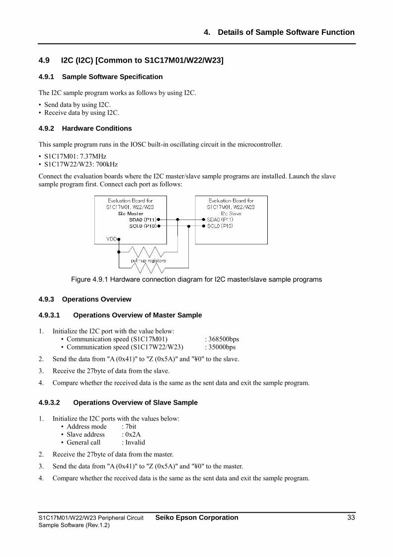
4.9 I2C (I2C) [Common to S1C17M01/W22/W23]
4.9.1 Sample Software Specification
The I2C sample program works as follows by using I2C.
• Send data by using I2C. • Receive data by using I2C. 4.9.2 Hardware Conditions
This sample program runs in the IOSC built-in oscillating circuit in the microcontroller.
• S1C17M01: 7.37MHz • S1C17W22/W23: 700kHz
Connect the evaluation boards where the I2C master/slave sample programs are installed. Launch the slave sample program first. Connect each port as follows:
Figure 4.9.1 Hardware connection diagram for I2C master/slave sample programs
4.9.3 Operations Overview
4.9.3.1 Operations Overview of Master Sample
1. Initialize the I2C port with the value below: • Communication speed (S1C17M01) : 368500bps • Communication speed (S1C17W22/W23) : 35000bps
2. Send the data from "A (0x41)" to "Z (0x5A)" and "¥0" to the slave.
3. Receive the 27byte of data from the slave.
4. Compare whether the received data is the same as the sent data and exit the sample program.
4.9.3.2 Operations Overview of Slave Sample
1. Initialize the I2C ports with the values below: • Address mode : 7bit • Slave address : 0x2A • General call : Invalid
2. Receive the 27byte of data from the master.
3. Send the data from "A (0x41)" to "Z (0x5A)" and "¥0" to the master.
4. Compare whether the received data is the same as the sent data and exit the sample program.
4. Details of Sample Software Function
34 Seiko Epson Corporation S1C17M01/W22/W23 Peripheral Circuit Sample Software (Rev.1.2)
4.10 LCD driver (LCD8A) [Only for S1C17M01]
4.10.1 Sample Software Specification
The LCD driver sample program is intended for S5U1C17M01T1. This sample program works as follows by using LCD8A.
• Turn on/off all lamps in normal display. • Turn on/off all lamps with all switch function. 4.10.2 Hardware Conditions
This sample program is intended for S5U1C17M01T1. For information on the connection with LCD panel, etc., refer to S5U1C17M01T1 Manual. This sample program runs in the OSC1 built-in oscillating circuit (32.768 kHz) in the microcontroller.
4.10.3 Operations Overview
1. Turn on all lamps for two seconds.
2. Turn off all lamps for two seconds.
3. Display "00000000" for two seconds on the segment.
4. Display "12345678" for two seconds on the segment.
5. Turn on the "battery warning" lamp for two seconds.
6. Turn on the "overflow warning" lamp for two seconds.
7. Turn on the "water-leak warning (up)" lamp for two seconds.
8. Turn on the "water-leak warning (down)" lamp for two seconds.
9. Turn on the "water-leak warning (up-down)" lamp for two seconds.
10. Turn on the "reverse flow warning (inside)" lamp for two seconds.
11. Turn on the "reverse flow warning (outside)" lamp for two seconds.
12. Turn on the "reverse flow warning (inside-outside)" lamp for two seconds.
13. Turn on the "unit ("m3/h")" lamp for two seconds.
14. Turn on the "communication" lamp for two seconds.
15. Turn on the "pilot" lamp for two seconds.
16. Turn off the segment for two seconds.
17. Display "Error" for two seconds on the segment.
18. Display "87654321" for two seconds on the segment.
19. Turn off LCD and exit the sample program.
4. Details of Sample Software Function
S1C17M01/W22/W23 Peripheral Circuit Seiko Epson Corporation 35 Sample Software (Rev.1.2)
4.11 LCD driver (LCD24A) [Only for S1C17W22]
4.11.1 Sample Software Specification
The LCD driver sample program is intended for S5U1C17W23T. This sample program works as follows by using LCD24A.
• Turn on/off all lamps in normal display. • Turn on/off all lamps with all switch function. 4.11.2 Hardware Conditions
This sample program is intended for S5U1C17W23T. For information on the connection with LCD panel, etc., refer to S5U1C17W23T Manual. This sample program runs in the OSC1 built-in oscillating circuit (32.768 kHz) in the microcontroller.
4.11.3 Operations Overview
1. Turn on all lamps for two seconds.
2. Turn off all lamps for two seconds.
3. Set a check pattern (small) in the display area 0.
4. Select the display area 0 and display the area for two seconds in normal mode.
5. Reverse display the area for two seconds.
6. Set a check pattern (medium) in the display area 1.
7. Select the display area 1 and display it for two seconds in normal mode.
8. Reverse display the area for two seconds.
9. Set a check pattern (large) in the display area 0.
10. Select the display area 0 and display it for two seconds in normal mode.
11. Reverse display the area for two seconds.
12. Turn off LCD and exit the sample program.

4. Details of Sample Software Function
36 Seiko Epson Corporation S1C17M01/W22/W23 Peripheral Circuit Sample Software (Rev.1.2)
4.12 R/F Converter (RFC) [Common to S1C17M01/W22/W23]
4.12.1 Sample Software Specification
The R/F converter sample program works as follows by using the R/F converter.
• Make the sensor's resistance CR oscillate, count the oscillation clock, and convert the oscillation into digital value.
4.12.2 Hardware Conditions
This sample program runs in the OSC1 built-in oscillating circuit (32.768 kHz) in the microcontroller. Before the use of this sample program, connect the board as follows:
Figure 4.12.1 Hardware connection diagram for R/F converter sample program (S1C17M01)
Figure 4.12.2 Hardware connection diagram for R/F converter sample program (S1C17W22/W23)
4.12.3 Operations Overview
1. Set external clock input mode and oscillation mode of RFC.
2. Initialize the measurement counter of R/F converter with 0x00fc0000 and start the measurement.
(measurement time : about 8 sec)
3. Get the measurement values from the reference and sensor oscillations and exit the sample program.
SENA0 (P04)
REF0 (P05)
RFIN0 (P06)
S1C17M01 evaluation board
SENA0 (P01)
REF0 (P02)
RFIN0 (P03)
S1C17W22/W23 evaluation board
4. Details of Sample Software Function
S1C17M01/W22/W23 Peripheral Circuit Seiko Epson Corporation 37 Sample Software (Rev.1.2)
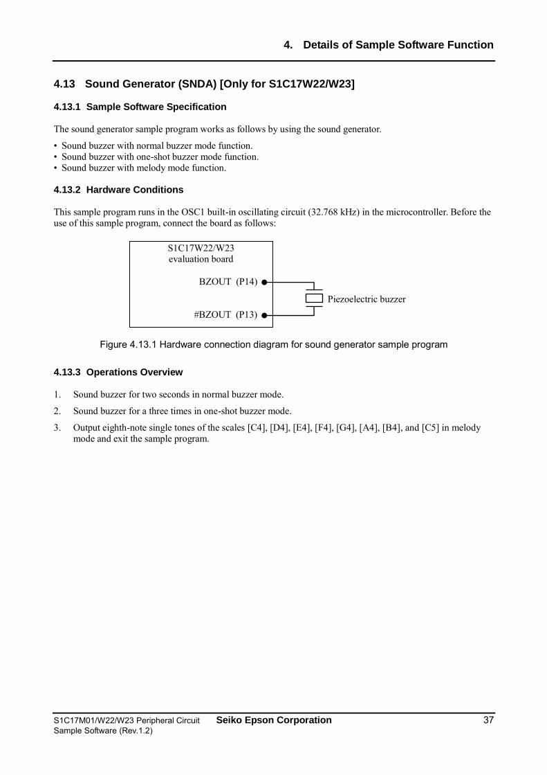
4.13 Sound Generator (SNDA) [Only for S1C17W22/W23]
4.13.1 Sample Software Specification
The sound generator sample program works as follows by using the sound generator.
• Sound buzzer with normal buzzer mode function. • Sound buzzer with one-shot buzzer mode function. • Sound buzzer with melody mode function. 4.13.2 Hardware Conditions
This sample program runs in the OSC1 built-in oscillating circuit (32.768 kHz) in the microcontroller. Before the use of this sample program, connect the board as follows:
Figure 4.13.1 Hardware connection diagram for sound generator sample program
4.13.3 Operations Overview
1. Sound buzzer for two seconds in normal buzzer mode.
2. Sound buzzer for a three times in one-shot buzzer mode.
3. Output eighth-note single tones of the scales [C4], [D4], [E4], [F4], [G4], [A4], [B4], and [C5] in melody mode and exit the sample program.
BZOUT (P14)
#BZOUT (P13)
S1C17W22/W23 evaluation board
Piezoelectric buzzer

4. Details of Sample Software Function
38 Seiko Epson Corporation S1C17M01/W22/W23 Peripheral Circuit Sample Software (Rev.1.2)
4.14 MR Sensor Controller (AMRC) [Only for S1C17M01]
4.14.1 Sample Software Specification
The MR sensor controller sample program works as follows by using the MR sensor controller.
• Count the number of passings of the magnet by using half-bridge MR sensor. • Count and memorize the number of passings of the magnet for a certain period of time to get a value
corresponding to the speed. • Output the signals for monitoring status to the pins below.
P00 : CMPIN0P < CMPIN0N: Output LOW / CMPIN0P > CMPIN0N: Output HIGH P01 : Low sample rate: Output LOW / High sample rate: Output HIGH EVPLS (P07) : Pilot pulse for detecting the change of magnetic field
4.14.2 Hardware Conditions
This sample program runs in the OSC1 built-in oscillating circuit (32.768 kHz) in the microcontroller. Before the use of this sample program, connect the board as follows:
Figure 4.14.1 Hardware connection diagram for MR sensor sample program (S1C17M01)
Tune the dial of semi-fixed resistance as follows by monitoring the voltage level at the pin P00 and confirm that the output value at the pin P00 changes according to whether magnetic field is applied to the sensor or not.
Resistance between CMPIN0N & GND 0 <---------------------------------------------------------------> Maximum Voltage level at pin P00 HHHHHHHHHHHHHHHLLLLLLLLLLLLLLLLLL Align with this position
4.14.3 Operations Overview
1. In normal condition, it is checked at a frequency of 32 times per second whether the applied magnetic field is changed in the MR sensor. (action when magnetic field change is not detected)
2. If it is confirmed that the applied magnetic field is changed in the MR sensor, the applied magnetic field is checked at a frequency of 1024 times per second. (if magnetic field change is detected, the sampling frequency increases)
3. If it is confirmed continuously for two seconds that the applied magnetic field is not changed, it moves to the normal mode where it is checked at a frequency of 32 times per second whether the applied magnetic field is changed. (if magnetic field is considered not changed, it returns to normal sampling frequency)
4. The components corresponding to the speed can be obtained by using the values of hbmrInfo.cntBuff[].
SENSEN (P21)
CMPIN0N (P17)
CMPIN0P (P20)
S1C17M01 evaluation board
Vcc
Vout
GND
Half-bridge MR sensor
Semi-fixed resistance (example: 50kΩ)
4. Details of Sample Software Function
S1C17M01/W22/W23 Peripheral Circuit Seiko Epson Corporation 39 Sample Software (Rev.1.2)
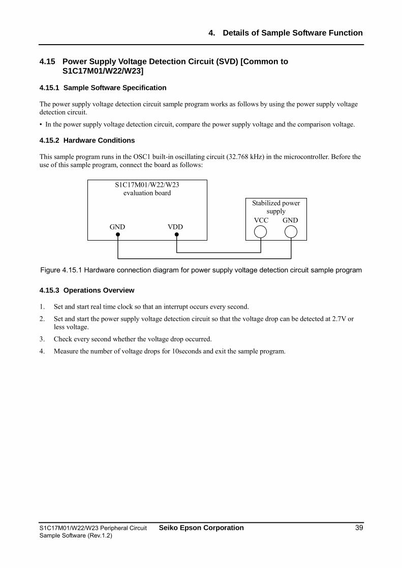
4.15 Power Supply Voltage Detection Circuit (SVD) [Common to S1C17M01/W22/W23]
4.15.1 Sample Software Specification
The power supply voltage detection circuit sample program works as follows by using the power supply voltage detection circuit.
• In the power supply voltage detection circuit, compare the power supply voltage and the comparison voltage. 4.15.2 Hardware Conditions
This sample program runs in the OSC1 built-in oscillating circuit (32.768 kHz) in the microcontroller. Before the use of this sample program, connect the board as follows:
Figure 4.15.1 Hardware connection diagram for power supply voltage detection circuit sample program
4.15.3 Operations Overview
1. Set and start real time clock so that an interrupt occurs every second.
2. Set and start the power supply voltage detection circuit so that the voltage drop can be detected at 2.7V or less voltage.
3. Check every second whether the voltage drop occurred.
4. Measure the number of voltage drops for 10seconds and exit the sample program.
S1C17M01/W22/W23 evaluation board
GND VDD
Stabilized power supply
VCC GND
4. Details of Sample Software Function
40 Seiko Epson Corporation S1C17M01/W22/W23 Peripheral Circuit Sample Software (Rev.1.2)
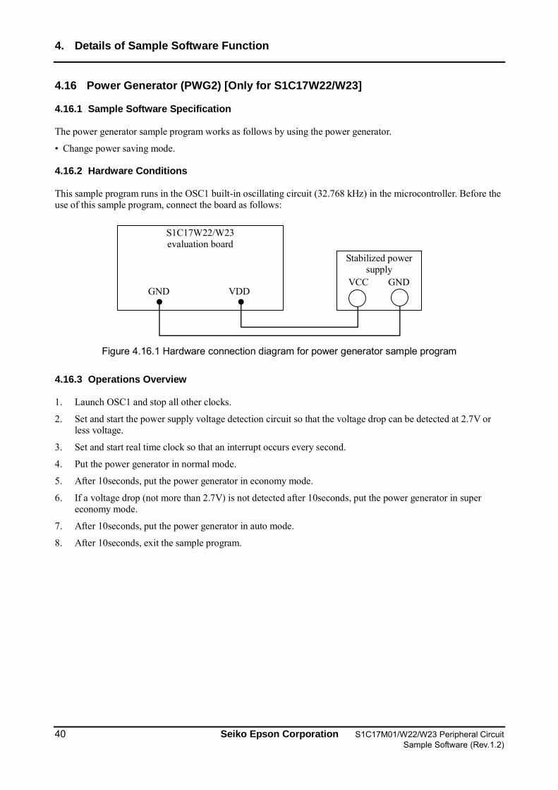
4.16 Power Generator (PWG2) [Only for S1C17W22/W23]
4.16.1 Sample Software Specification
The power generator sample program works as follows by using the power generator.
• Change power saving mode. 4.16.2 Hardware Conditions
This sample program runs in the OSC1 built-in oscillating circuit (32.768 kHz) in the microcontroller. Before the use of this sample program, connect the board as follows:
Figure 4.16.1 Hardware connection diagram for power generator sample program
4.16.3 Operations Overview
1. Launch OSC1 and stop all other clocks.
2. Set and start the power supply voltage detection circuit so that the voltage drop can be detected at 2.7V or less voltage.
3. Set and start real time clock so that an interrupt occurs every second.
4. Put the power generator in normal mode.
5. After 10seconds, put the power generator in economy mode.
6. If a voltage drop (not more than 2.7V) is not detected after 10seconds, put the power generator in super economy mode.
7. After 10seconds, put the power generator in auto mode.
8. After 10seconds, exit the sample program.
S1C17W22/W23 evaluation board
GND VDD
Stabilized power supply
VCC GND
4. Details of Sample Software Function
S1C17M01/W22/W23 Peripheral Circuit Seiko Epson Corporation 41 Sample Software (Rev.1.2)
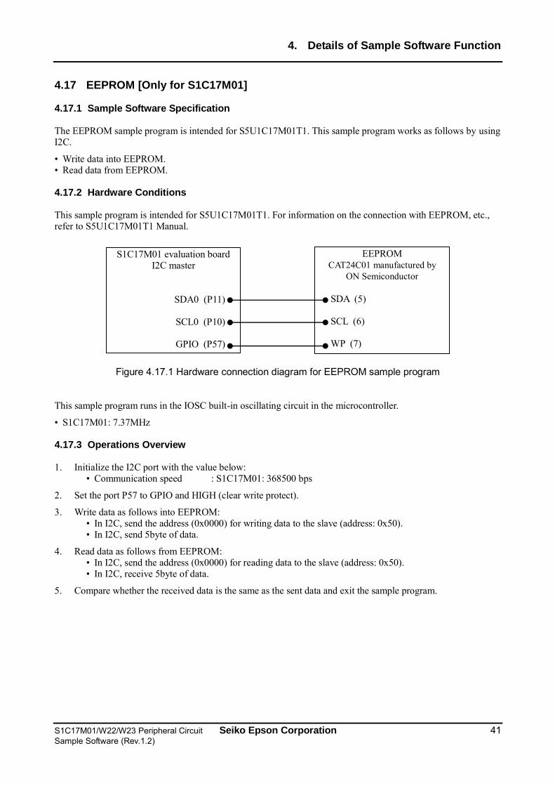
4.17 EEPROM [Only for S1C17M01]
4.17.1 Sample Software Specification
The EEPROM sample program is intended for S5U1C17M01T1. This sample program works as follows by using I2C.
• Write data into EEPROM. • Read data from EEPROM. 4.17.2 Hardware Conditions
This sample program is intended for S5U1C17M01T1. For information on the connection with EEPROM, etc., refer to S5U1C17M01T1 Manual.
Figure 4.17.1 Hardware connection diagram for EEPROM sample program
This sample program runs in the IOSC built-in oscillating circuit in the microcontroller.
• S1C17M01: 7.37MHz 4.17.3 Operations Overview
1. Initialize the I2C port with the value below: • Communication speed : S1C17M01: 368500 bps
2. Set the port P57 to GPIO and HIGH (clear write protect).
3. Write data as follows into EEPROM: • In I2C, send the address (0x0000) for writing data to the slave (address: 0x50). • In I2C, send 5byte of data.
4. Read data as follows from EEPROM: • In I2C, send the address (0x0000) for reading data to the slave (address: 0x50). • In I2C, receive 5byte of data.
5. Compare whether the received data is the same as the sent data and exit the sample program.
SDA0 (P11)
SCL0 (P10)
GPIO (P57)
S1C17M01 evaluation board I2C master
SDA (5) SCL (6) WP (7)
EEPROM CAT24C01 manufactured by
ON Semiconductor
4. Details of Sample Software Function
42 Seiko Epson Corporation S1C17M01/W22/W23 Peripheral Circuit Sample Software (Rev.1.2)
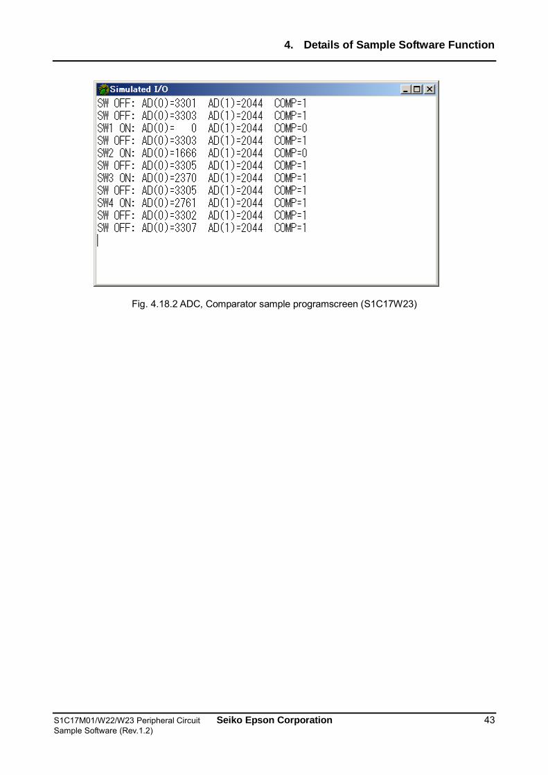
4.18 ADC, Comparator [Only for S1C17W23]
4.18.1 Sample Software Specification
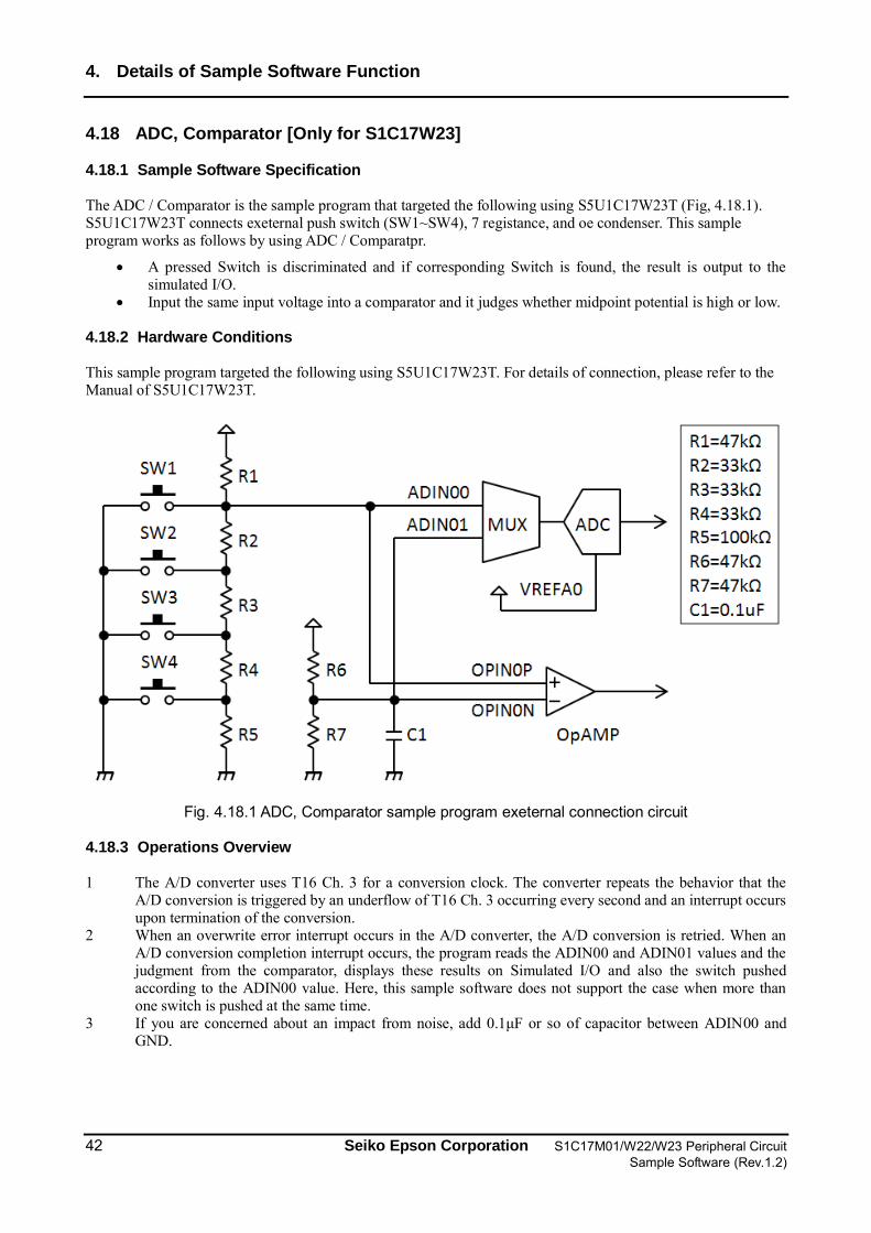
The ADC / Comparator is the sample program that targeted the following using S5U1C17W23T (Fig, 4.18.1). S5U1C17W23T connects exeternal push switch (SW1~SW4), 7 registance, and oe condenser. This sample program works as follows by using ADC / Comparatpr.
A pressed Switch is discriminated and if corresponding Switch is found, the result is output to the simulated I/O.
Input the same input voltage into a comparator and it judges whether midpoint potential is high or low. 4.18.2 Hardware Conditions
This sample program targeted the following using S5U1C17W23T. For details of connection, please refer to the Manual of S5U1C17W23T.
Fig. 4.18.1 ADC, Comparator sample program exeternal connection circuit
4.18.3 Operations Overview
1 The A/D converter uses T16 Ch. 3 for a conversion clock. The converter repeats the behavior that the A/D conversion is triggered by an underflow of T16 Ch. 3 occurring every second and an interrupt occurs upon termination of the conversion.
2 When an overwrite error interrupt occurs in the A/D converter, the A/D conversion is retried. When an A/D conversion completion interrupt occurs, the program reads the ADIN00 and ADIN01 values and the judgment from the comparator, displays these results on Simulated I/O and also the switch pushed according to the ADIN00 value. Here, this sample software does not support the case when more than one switch is pushed at the same time.
3 If you are concerned about an impact from noise, add 0.1μF or so of capacitor between ADIN00 and GND.
4. Details of Sample Software Function
S1C17M01/W22/W23 Peripheral Circuit Seiko Epson Corporation 43 Sample Software (Rev.1.2)
Fig. 4.18.2 ADC, Comparator sample programscreen (S1C17W23)
4. Details of Sample Software Function
44 Seiko Epson Corporation S1C17M01/W22/W23 Peripheral Circuit Sample Software (Rev.1.2)
4.19 REMC [Common to S1C17W22/W23]
4.19.1 Sample Software Specification
The REMC sample program generates signals for infrared ray remote-controller by using REMC mounted on the S1C17W23 evaluation board (SVT17W23). This sample program performs the following operations by using REMC.
Move to a sleep mode after initialization and wait for interrupts triggered by push switches SW1 to SW4 (connected to P07 to P04).
When an interrupt is caused by SW1 to SW4, analyze which switch was pushed and accordingly generate a signal (frame signal) for infrared ray remote-controller on REMC. Then, activate the T16 Ch.0 timer and check the switch status after about 108ms.
If the same key was pushed consecutively when an interrupt occurred at the T16 Ch.0 timer, generate a repeat signal and set the T16 Ch.0 timer so that the switch status is checked again after about 108ms. Otherwise, stop the T16 Ch.0 timer and REMC, enter into a sleep mode, and wait for interrupts triggered by switches SW1 to SW4.
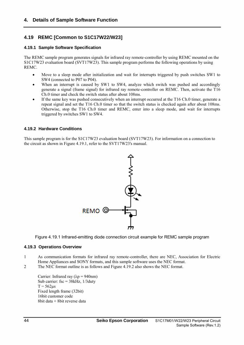
4.19.2 Hardware Conditions
This sample program is for the S1C17W23 evaluation board (SVT17W23). For information on a connection to the circuit as shown in Figure 4.19.1, refer to the SVT17W23's manual.
Figure 4.19.1 Infrared-emitting diode connection circuit example for REMC sample program 4.19.3 Operations Overview
1 As communication formats for infrared ray remote-controller, there are NEC, Association for Electric Home Appliances and SONY formats, and this sample software uses the NEC format.
2 The NEC format outline is as follows and Figure 4.19.2 also shows the NEC format. Carrier: Infrared ray (λp = 940nm) Sub carrier: fsc = 38kHz, 1/3duty T = 562µs Fixed length frame (32bit) 16bit customer code 8bit data + 8bit reverse data

4. Details of Sample Software Function
S1C17M01/W22/W23 Peripheral Circuit Seiko Epson Corporation 45 Sample Software (Rev.1.2)
Figure 4.19.2 Signal waveform of NEC format
3 REMC determines the data waveform shape by two parameters: APLEN (data signal duty) and DBLEN (data signal cycle). Each of APLEN and DBLEN defines the waveform shape with 34 frame signals and 2 repeat signals and allocates the leader, customer code, and repeat signals common to push switches SW1 to SW4 at initialization. Since the 16 values at data part may vary according to SW1 to SW4, the data values are allocated when an interrupt occurs by pushing a switch.
4 This sample program uses the OSC3 behavior at 4MHz. Set a GPIO mode for push switches SW1 to SW4, allocate ports for REMO, initialize T16 Ch.0, and enter into a sleep mode to wait for interrupts caused by pushing switches SW1 to SW4.
5 When an interrupt occurs, analyze which switch was pushed and allocate APLEN and DBLEN values in data part according to the switch pushed. Since REMC uses a buffer mode, activate REMC after initialization. Also, activate T16 Ch.0 and generate a T16 Ch.0 interrupt after about 108ms.
6 When a compare DB interrupt occurs at REMC, write the following APLEN and DBLEN data into register. When writing last but one piece of data, change REMC to a one-shot mode to prevent the whisker-like signal output. At the last data, stop the REMC operation.
7 When a T16 Ch.0 interrupt occurred, check whether the same switch SW1 to SW4 was pushed. If the same switch was pushed, set the register values of REMC so that a repeat waveform is generated, initialize REMC before activation, and activate REMC. Otherwise, stop the T16 Ch.0 operation.
Revision History
46 Seiko Epson Corporation S1C17M01/W22/W23 Peripheral Circuit Sample Software (Rev.1.2)
Revision History
Attachment-1 Rev. No. Date Page Category Contents
Rev. 1.0 2013/12/5 All new
Rev. 1.1 2014/7/25 Page 12 Addition Added a note to terminate the program that controls the clocks or related functions.
Page 13 Modify Modified the evaluation board name in Figure 4.1.1.
Page 21 Replacement Replaced Figure 4.4.1 according to the corrected T16B sample driver.
Page 23 Modify Replaced “NMI interrupt” with “reset interrupt.” Modified the description in Operations Overview No. 4.
Page 37 Modify Replaced [only for S1C17W23] with [Common to S1C17W22/W23] as a target model was added.
Rev. 1.2 2015/12/8 Overall Addition Added descriptions relating to the operating environment (GNU17 version 2/version 3 , ICDmini ver. 2.0/ver. 3.0), as a new operating environment has been supported.
International Sales Operations
AMERICA EPSON ELECTRONICS AMERICA, INC.
214 Devcon Drive, San Jose, CA 95112, USA Phone: +1-800-228-3964 FAX: +1-408-922-0238 EUROPE EPSON EUROPE ELECTRONICS GmbH
Riesstrasse 15, 80992 Munich, GERMANY Phone: +49-89-14005-0 FAX: +49-89-14005-110
ASIA EPSON (CHINA) CO., LTD. 7F, Jinbao Bldg., No.89 Jinbao St., Dongcheng District, Beijing 100005, CHINA Phone: +86-10-8522-1199 FAX: +86-10-8522-1125 SHANGHAI BRANCH 7F, Block B, Hi-Tech Bldg., 900 Yishan Road, Shanghai 200233, CHINA Phone: +86-21-5423-5577 FAX: +86-21-5423-4677 SHENZHEN BRANCH 12F, Dawning Mansion, Keji South 12th Road, Hi-Tech Park, Shenzhen 518057, CHINA Phone: +86-755-2699-3828 FAX: +86-755-2699-3838 EPSON TAIWAN TECHNOLOGY & TRADING LTD. 14F, No. 7, Song Ren Road, Taipei 110, TAIWAN Phone: +886-2-8786-6688 FAX: +886-2-8786-6660 EPSON SINGAPORE PTE., LTD. 1 HarbourFront Place, #03-02 HarbourFront Tower One, Singapore 098633 Phone: +65-6586-5500 FAX: +65-6271-3182 SEIKO EPSON CORP.
KOREA OFFICE 5F, KLI 63 Bldg., 60 Yoido-dong, Youngdeungpo-Ku, Seoul 150-763, KOREA Phone: +82-2-784-6027 FAX: +82-2-767-3677 SEIKO EPSON CORP.
MICRODEVICES OPERATIONS DIVISION Device Sales & Marketing Department 421-8, Hino, Hino-shi, Tokyo 191-8501, JAPAN Phone: +81-42-587-5816 FAX: +81-42-587-5117
Document Code: 412444402 First Issue December 2013 ○V
Revised December in JAPAN 2015 ○L