S-8254A SERIES BATTREY PROTECTION IC - …beriled.biz/data/files/S8254A_E.pdf · BATTERY PROTECTION...
29
S-8254A Series www.sii-ic.com BATTERY PROTECTION IC FOR 3-SERIAL- OR 4-SERIAL-CELL PACK © Seiko Instruments Inc., 2002-2010 Rev.5.0_01 Seiko Instruments Inc. 1 The S-8254A series is a protection IC for 3-serial- or 4-serial-cell lithium-ion / lithium polymer rechargeable batteries and includes a high-accuracy voltage detector and delay circuit. The S-8254A series protects both 3-serial or 4-serial cells using the SEL pin for switching. Features (1) High-accuracy voltage detection for each cell • Overcharge detection voltage n (n = 1 to 4) 3.9 V to 4.4 V (50 mV steps) Accuracy ±25 mV • Overcharge release voltage n (n = 1 to 4) 3.8 V to 4.4 V *1 Accuracy ±50 mV • Overdischarge detection voltage n (n = 1 to 4) 2.0 V to 3.0 V (100 mV steps) Accuracy ±80 mV • Overdischarge release voltage n (n = 1 to 4) 2.0 V to 3.4 V *2 Accuracy ±100 mV (2) Three-level overcurrent protection • Overcurrent detection voltage 1 0.05 V to 0.30 V (50 mV steps) Accuracy ±25 mV • Overcurrent detection voltage 2 0.5 V Accuracy ±100 mV • Overcurrent detection voltage 3 V VC1 − 1.2 V Accuracy ±300 mV (3) Delay times for overcharge detection, overdischarge detection and overcurrent detection 1 can be set by external capacitors (delay times for overcurrent detection 2 and 3 are fixed internally). (4) Switchable between a 3-serial cell and 4-serial cell using the SEL pin (5) Charge/discharge operation can be controlled via the control pins. (6) High-withstand voltage device Absolute maximum rating : 26 V (7) Wide operating voltage range 2 V to 24 V (8) Wide operating temperature range −40°C to + 85°C (9) Low current consumption • Operation mode 30 μA max. (+25°C) • Power-down mode 0.1 μA max. (+25°C) (10) Lead-free, Sn100%, halogen-free *3 *1. Overcharge hysteresis voltage n (n = 1 to 4) can be selected as 0 V or from a range of 0.1 V to 0.4 V in 50 mV steps. (Overcharge hysteresis voltage = Overcharge detection voltage − Overcharge release voltage) *2. Overdischarge hysteresis voltage n (n = 1 to 4) can be selected as 0 V or from a range of 0.2 V to 0.7 V in 100 mV steps. (Overdischarge hysteresis voltage = Overdischarge release voltage − Overdischarge detection voltage) *3. Refer to “ Product Name Structure” for details. Applications • Lithium-ion rechargeable battery packs • Lithium polymer rechargeable battery packs Package • 16-Pin TSSOP
-
Upload
vuongxuyen -
Category
Documents
-
view
214 -
download
0
Transcript of S-8254A SERIES BATTREY PROTECTION IC - …beriled.biz/data/files/S8254A_E.pdf · BATTERY PROTECTION...

S-8254A Series
www.sii-ic.com
BATTERY PROTECTION ICFOR 3-SERIAL- OR 4-SERIAL-CELL PACK
© Seiko Instruments Inc., 2002-2010 Rev.5.0_01
Seiko Instruments Inc. 1
The S-8254A series is a protection IC for 3-serial- or 4-serial-cell lithium-ion / lithium polymer rechargeable batteries and includes a high-accuracy voltage detector and delay circuit. The S-8254A series protects both 3-serial or 4-serial cells using the SEL pin for switching.
Features (1) High-accuracy voltage detection for each cell
• Overcharge detection voltage n (n = 1 to 4) 3.9 V to 4.4 V (50 mV steps) Accuracy ±25 mV • Overcharge release voltage n (n = 1 to 4) 3.8 V to 4.4 V*1 Accuracy ±50 mV • Overdischarge detection voltage n (n = 1 to 4) 2.0 V to 3.0 V (100 mV steps) Accuracy ±80 mV • Overdischarge release voltage n (n = 1 to 4) 2.0 V to 3.4 V*2 Accuracy ±100 mV
(2) Three-level overcurrent protection • Overcurrent detection voltage 1 0.05 V to 0.30 V (50 mV steps) Accuracy ±25 mV • Overcurrent detection voltage 2 0.5 V Accuracy ±100 mV • Overcurrent detection voltage 3 VVC1 − 1.2 V Accuracy ±300 mV
(3) Delay times for overcharge detection, overdischarge detection and overcurrent detection 1 can be set by external capacitors (delay times for overcurrent detection 2 and 3 are fixed internally).
(4) Switchable between a 3-serial cell and 4-serial cell using the SEL pin (5) Charge/discharge operation can be controlled via the control pins. (6) High-withstand voltage device Absolute maximum rating : 26 V (7) Wide operating voltage range 2 V to 24 V (8) Wide operating temperature range −40°C to + 85°C (9) Low current consumption
• Operation mode 30 μA max. (+25°C) • Power-down mode 0.1 μA max. (+25°C)
(10) Lead-free, Sn100%, halogen-free*3
*1. Overcharge hysteresis voltage n (n = 1 to 4) can be selected as 0 V or from a range of 0.1 V to 0.4 V in 50 mV steps. (Overcharge hysteresis voltage = Overcharge detection voltage − Overcharge release voltage)
*2. Overdischarge hysteresis voltage n (n = 1 to 4) can be selected as 0 V or from a range of 0.2 V to 0.7 V in 100 mV steps. (Overdischarge hysteresis voltage = Overdischarge release voltage − Overdischarge detection voltage)
*3. Refer to “ Product Name Structure” for details.
Applications
• Lithium-ion rechargeable battery packs • Lithium polymer rechargeable battery packs
Package
• 16-Pin TSSOP

BATTERY PROTECTION IC FOR 3-SERIAL- OR 4-SERIAL-CELL PACK S-8254A Series Rev.5.0_01
Seiko Instruments Inc. 2
Block Diagram
COP
VDD
VSS
VMP
DOP
VINI
CDT
VC1
VC2
VC3
−+
+ −
−+
+−
−+
+−
−+
+−
CTL
SEL
VC4
DOP, COP, RVMD, RVMS
Control Circuit
+ −
+−
+ −
Delay Circuit
Delay Circuit
Delay Circuit
Delay Circuit1 MΩ
900 kΩ
CCT 200 nA
Remark 1. Diodes in the figure are parasitic diodes.
2. Numerical values are typical values.
Figure 1
BATTERY PROTECTION IC FOR 3-SERIAL- OR 4-SERIAL-CELL PACKRev.5.0_01 S-8254A Series
Seiko Instruments Inc. 3
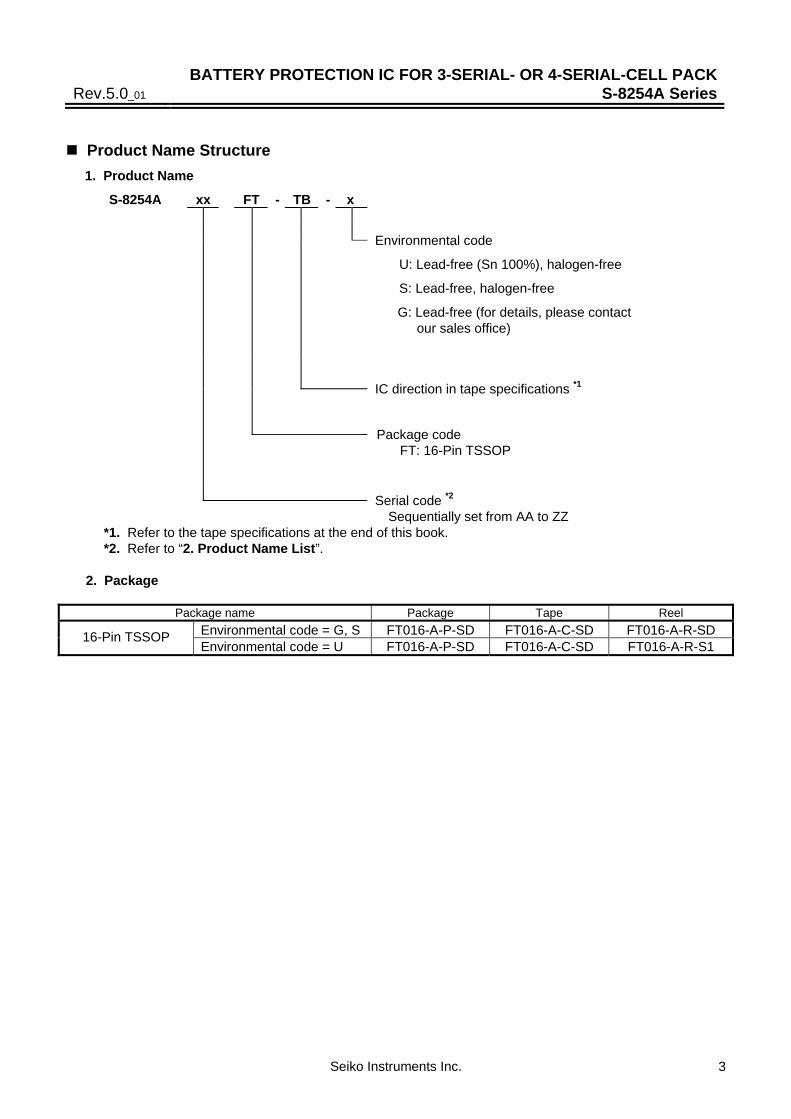
Product Name Structure
1. Product Name
S-8254A xx FT - TB - x
Environmental code
U: Lead-free (Sn 100%), halogen-free
S: Lead-free, halogen-free
G: Lead-free (for details, please contact our sales office)
IC direction in tape specifications *1
Package code FT: 16-Pin TSSOP
Serial code *2 Sequentially set from AA to ZZ
*1. Refer to the tape specifications at the end of this book. *2. Refer to “2. Product Name List”.
2. Package
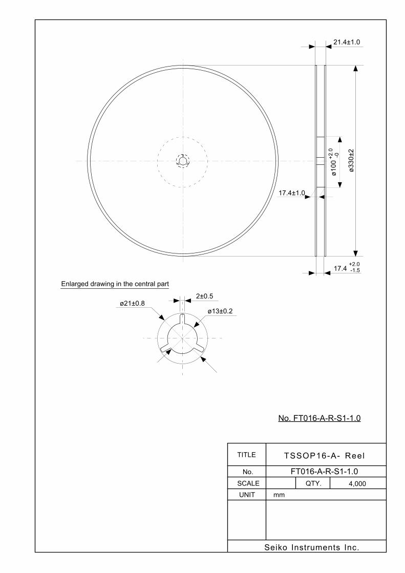
Package name Package Tape Reel Environmental code = G, S FT016-A-P-SD FT016-A-C-SD FT016-A-R-SD 16-Pin TSSOP Environmental code = U FT016-A-P-SD FT016-A-C-SD FT016-A-R-S1

BATTERY PROTECTION IC FOR 3-SERIAL- OR 4-SERIAL-CELL PACK S-8254A Series Rev.5.0_01
Seiko Instruments Inc. 4
2. Product Name List
Table 1
Product name / Item
Overcharge detection voltage
[VCU]
Overcharge release voltage
[VCL]
Overdischarge detection voltage
[VDL]
Overdischarge release voltage
[VDU]
Overcurrent detection voltage 1
[VIOV1]
0 V battery charge function
S-8254AAAFT-TB-x 4.350 ± 0.025 V 4.150 ± 0.050 V 2.00 ± 0.080 V 2.70 ± 0.100 V 0.30 ± 0.025 V Available S-8254AABFT-TB-x 4.250 ± 0.025 V 4.250 ± 0.025 V 2.00 ± 0.080 V 2.70 ± 0.100 V 0.30 ± 0.025 V Available S-8254AAEFT-TB-x 4.350 ± 0.025 V 4.150 ± 0.050 V 2.00 ± 0.080 V 2.70 ± 0.100 V 0.20 ± 0.025 V Available S-8254AAFFT-TB-x 4.350 ± 0.025 V 4.150 ± 0.050 V 2.40 ± 0.080 V 3.00 ± 0.100 V 0.20 ± 0.025 V Available S-8254AAGFT-TB-x 4.275 ± 0.025 V 4.075 ± 0.050 V 2.30 ± 0.080 V 2.70 ± 0.100 V 0.13 ± 0.025 V Available S-8254AAHFT-TB-x 4.350 ± 0.025 V 4.150 ± 0.050 V 2.40 ± 0.080 V 2.70 ± 0.100 V 0.10 ± 0.025 V Available S-8254AAIFT-TB-x 4.350 ± 0.025 V 4.150 ± 0.050 V 2.40 ± 0.080 V 3.00 ± 0.100 V 0.30 ± 0.025 V Available S-8254AAJFT-TB-x 4.350 ± 0.025 V 4.150 ± 0.050 V 2.40 ± 0.080 V 3.00 ± 0.100 V 0.15 ± 0.025 V Available S-8254AAKFT-TB-x 4.350 ± 0.025 V 4.150 ± 0.050 V 2.70 ± 0.080 V 3.00 ± 0.100 V 0.20 ± 0.025 V Available S-8254AALFT-TB-x 4.300 ± 0.025 V 4.150 ± 0.050 V 2.40 ± 0.080 V 3.00 ± 0.100 V 0.20 ± 0.025 V Available S-8254AAMFT-TB-x 4.200 ± 0.025 V 4.100 ± 0.050 V 2.50 ± 0.080 V 2.70 ± 0.100 V 0.30 ± 0.025 V Available S-8254AANFT-TB-x 4.250 ± 0.025 V 4.150 ± 0.050 V 2.50 ± 0.080 V 3.00 ± 0.100 V 0.10 ± 0.025 V Available S-8254AAOFT-TB-X 4.300 ± 0.025 V 4.080 ± 0.050 V 2.50 ± 0.080 V 3.00 ± 0.100 V 0.10 ± 0.025 V Available S-8254AAPFT-TB-x 4.280 ± 0.025 V 4.130 ± 0.050 V 3.00 ± 0.080 V 3.00 ± 0.080 V 0.15 ± 0.025 V Available S-8254AAQFT-TB-x 3.900 ± 0.025 V 3.800 ± 0.050 V 2.30 ± 0.080 V 2.70 ± 0.100 V 0.30 ± 0.025 V Available S-8254AARFT-TB-x 4.350 ± 0.025 V 4.150 ± 0.050 V 2.80 ± 0.080 V 3.00 ± 0.100 V 0.20 ± 0.025 V Available S-8254AASFT-TB-x 4.290 ± 0.025 V 4.090 ± 0.050 V 2.30 ± 0.080 V 3.00 ± 0.100 V 0.075 ± 0.025 V Available S-8254AATFT-TB-x 4.200 ± 0.025 V 4.200 ± 0.025 V 2.00 ± 0.080 V 2.70 ± 0.100 V 0.30 ± 0.025 V Available
S-8254AAUFT-TB-x 4.350 ± 0.025 V 4.150 ± 0.050 V 2.40 ± 0.080 V 3.00 ± 0.100 V 0.20 ± 0.025 V Unavailable S-8254AAVFT-TB-x 4.250 ± 0.025 V 4.150 ± 0.050 V 2.70 ± 0.080 V 3.00 ± 0.100 V 0.20 ± 0.025 V Available S-8254AAWFT-TB-x 4.250 ± 0.025 V 4.100 ± 0.050 V 3.00 ± 0.080 V 3.20 ± 0.100 V 0.10 ± 0.025 V Unavailable S-8254AAXFT-TB-x 4.250 ± 0.025 V 4.100 ± 0.050 V 2.00 ± 0.080 V 2.70 ± 0.100 V 0.15 ± 0.025 V Available S-8254AAYFT-TB-x 4.275 ± 0.025 V 4.125 ± 0.050 V 2.40 ± 0.080 V 2.70 ± 0.100 V 0.10 ± 0.025 V Available S-8254AAZFT-TB-x 4.250 ± 0.025 V 4.150 ± 0.050 V 2.00 ± 0.080 V 2.70 ± 0.100 V 0.13 ± 0.025 V Available S-8254ABAFT-TB-x 3.900 ± 0.025 V 3.800 ± 0.050 V 2.00 ± 0.080 V 2.50 ± 0.100 V 0.15 ± 0.025 V Available S-8254ABBFT-TB-x 4.200 ± 0.025 V 4.200 ± 0.025 V 2.50 ± 0.080 V 3.20 ± 0.100 V 0.30 ± 0.025 V Available S-8254ABCFT-TB-x 4.175 ± 0.025 V 3.975 ± 0.050 V 2.75 ± 0.080 V 3.05 ± 0.100 V 0.10 ± 0.025 V Available S-8254ABDFT-TB-y 4.300 ± 0.025 V 4.100 ± 0.050 V 2.00 ± 0.080 V 2.00 ± 0.080 V 0.13 ± 0.025 V Available S-8254ABEFT-TB-y 4.200 ± 0.025 V 4.150 ± 0.050 V 2.50 ± 0.080 V 3.00 ± 0.100 V 0.15 ± 0.025 V Available S-8254ABFFT-TB-x 4.150 ± 0.025 V 4.050 ± 0.050 V 2.00 ± 0.080 V 2.70 ± 0.100 V 0.13 ± 0.025 V Available S-8254ABGFT-TB-x 4.180 ± 0.025 V 4.080 ± 0.050 V 2.00 ± 0.080 V 2.70 ± 0.100 V 0.13 ± 0.025 V Available S-8254ABHFT-TB-y 4.150 ± 0.025 V 4.050 ± 0.050 V 2.50 ± 0.080 V 2.80 ± 0.100 V 0.10 ± 0.025 V Available S-8254ABIFT-TB-x 4.215 ± 0.025 V 4.115 ± 0.050 V 2.40 ± 0.080 V 3.00 ± 0.100 V 0.20 ± 0.025 V Unavailable
Remark 1. Please contact our sales office for the products with the detection voltage value other than those specified above.
2. x: G or U y: S or U
3. Please select products of environmental code = U for Sn 100%, halogen-free products.
BATTERY PROTECTION IC FOR 3-SERIAL- OR 4-SERIAL-CELL PACKRev.5.0_01 S-8254A Series
Seiko Instruments Inc. 5
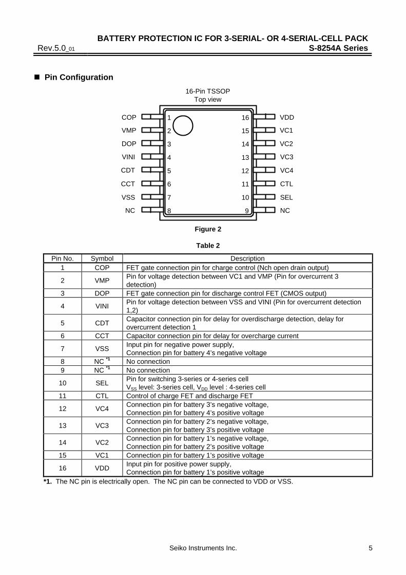
Pin Configuration
16-Pin TSSOP Top view
8
7
6
5
3
2
4
1
11
16
9
10
12
14
15
13
COP
VMP
DOP
VINI
CDT
CCT
VSS
NC
VDD
VC1
VC2
VC3
VC4
CTL
SEL
NC
Figure 2
Table 2
Pin No. Symbol Description 1 COP FET gate connection pin for charge control (Nch open drain output)
2 VMP Pin for voltage detection between VC1 and VMP (Pin for overcurrent 3 detection)
3 DOP FET gate connection pin for discharge control FET (CMOS output)
4 VINI Pin for voltage detection between VSS and VINI (Pin for overcurrent detection 1,2)
5 CDT Capacitor connection pin for delay for overdischarge detection, delay for overcurrent detection 1
6 CCT Capacitor connection pin for delay for overcharge current
7 VSS Input pin for negative power supply, Connection pin for battery 4’s negative voltage
8 NC *1 No connection 9 NC *1 No connection
10 SEL Pin for switching 3-series or 4-series cell VSS level: 3-series cell, VDD level : 4-series cell
11 CTL Control of charge FET and discharge FET
12 VC4 Connection pin for battery 3’s negative voltage, Connection pin for battery 4’s positive voltage
13 VC3 Connection pin for battery 2’s negative voltage, Connection pin for battery 3’s positive voltage
14 VC2 Connection pin for battery 1’s negative voltage, Connection pin for battery 2’s positive voltage
15 VC1 Connection pin for battery 1’s positive voltage
16 VDD Input pin for positive power supply, Connection pin for battery 1’s positive voltage
*1. The NC pin is electrically open. The NC pin can be connected to VDD or VSS.
BATTERY PROTECTION IC FOR 3-SERIAL- OR 4-SERIAL-CELL PACK S-8254A Series Rev.5.0_01
Seiko Instruments Inc. 6
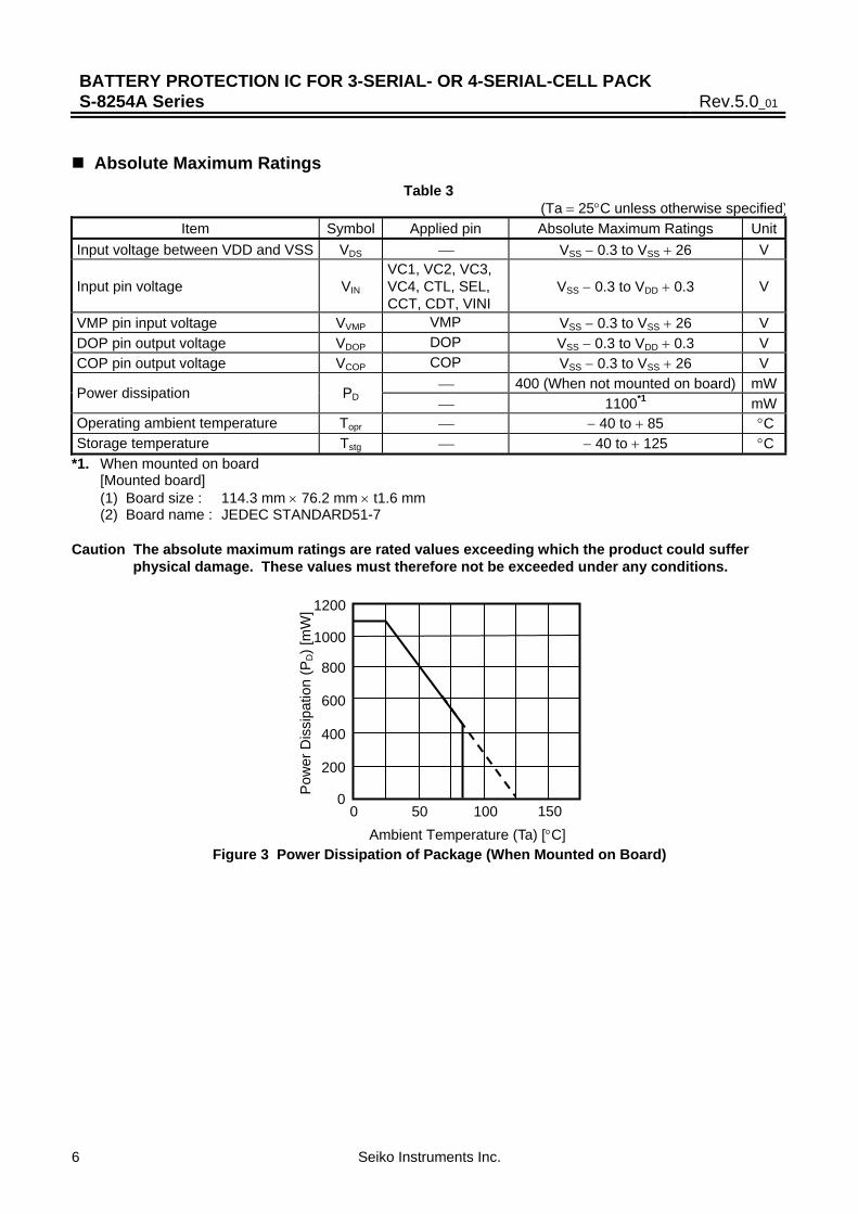
Absolute Maximum Ratings
Table 3 (Ta = 25°C unless otherwise specified)
Item Symbol Applied pin Absolute Maximum Ratings UnitInput voltage between VDD and VSS VDS ⎯ VSS − 0.3 to VSS + 26 V
Input pin voltage VIN VC1, VC2, VC3, VC4, CTL, SEL, CCT, CDT, VINI
VSS − 0.3 to VDD + 0.3 V
VMP pin input voltage VVMP VMP VSS − 0.3 to VSS + 26 V DOP pin output voltage VDOP DOP VSS − 0.3 to VDD + 0.3 V COP pin output voltage VCOP COP VSS − 0.3 to VSS + 26 V
⎯ 400 (When not mounted on board) mWPower dissipation PD ⎯ 1100*1 mW
Operating ambient temperature Topr ⎯ − 40 to + 85 °C Storage temperature Tstg ⎯ − 40 to + 125 °C
*1. When mounted on board [Mounted board] (1) Board size : 114.3 mm × 76.2 mm × t1.6 mm (2) Board name : JEDEC STANDARD51-7 Caution The absolute maximum ratings are rated values exceeding which the product could suffer
physical damage. These values must therefore not be exceeded under any conditions.
0 50 100 150
800
400
0 Pow
er D
issi
patio
n (P
D) [
mW
]
Ambient Temperature (Ta) [°C]
1000
600
200
1200
Figure 3 Power Dissipation of Package (When Mounted on Board)

BATTERY PROTECTION IC FOR 3-SERIAL- OR 4-SERIAL-CELL PACKRev.5.0_01 S-8254A Series
Seiko Instruments Inc. 7
Electrical Characteristics
Table 4 (1 / 2) (Ta = 25°C unless otherwise specified)
Item Symbol Conditions Min. Typ. Max. Unit Test circuit
[ DETECTION VOLTAGE ] Overcharge detection voltage n (n = 1, 2, 3, 4) VCUn 3.9 V to 4.4 V, Adjustable VCUn
− 0.025 VCUn VCUn
+ 0.025 V 2
VCLn VCL ≠ VCU VCLn − 0.05 VCLn
VCLn + 0.05 V 2 Overcharge release voltage n
(n = 1, 2, 3, 4)
3.8 V to 4.4 V, Adjustable
VCL = VCU VCLn − 0.025 VCLn
VCLn + 0.025 V 2
Overdischarge detection voltage n(n = 1, 2, 3, 4) VDLn 2.0 V to 3.0 V, Adjustable VDLn
− 0.08 VDLn VDLn
+ 0.08 V 2
VDUn VDL ≠ VDU VDUn − 0.10 VDUn
VDUn + 0.10 V 2 Overdischarge release voltage n
(n = 1, 2, 3, 4)
2.0 V to 3.4 V, Adjustable
VDL = VDU VDUn − 0.08 VDUn
VDUn + 0.08 V 2
Overcurrent detection voltage 1 VIOV1 0.05 V to 0.3 V, Adjustable VIOV1 − 0.025 VIOV1
VIOV1 + 0.025 V 2
Overcurrent detection voltage 2 VIOV2 ⎯ 0.4 0.5 0.6 V 2
Overcurrent detection voltage 3 VIOV3 ⎯ VVC1 − 1.5
VVC1
− 1.2 VVC1 − 0.9 V 2
Temperature coefficient 1 *1 TCOE1 Ta = 0°C to 50°C *3 − 1.0 0 1.0 mV / °C 2 Temperature coefficient 2 *2 TCOE2 Ta = 0°C to 50°C *3 − 0.5 0 0.5 mV / °C 2
[ DELAY TIME ] Overcharge detection delay time tCU CCT pin capacitance = 0.1 μF 0.5 1.0 1.5 s 3 Overdischarge detection delay time tDL CDT pin capacitance = 0.1 μF 50 100 150 ms 3
Overcurrent detection delay time 1 tIOV1 CDT pin capacitance = 0.1 μF 5 10 15 ms 3
Overcurrent detection delay time 2 tIOV2 ⎯ 0.4 1 1.6 ms 3
Overcurrent detection delay time 3 tIOV3 FET gate capacitance = 2000 pF 100 300 600 μs 3
[ 0 V BATTERY CHARGE FUNCTION ] 0 V battery charge starting charger voltage V0CHA 0 V battery charging available ⎯ 0.8 1.5 V 4
0 V battery charge inhibition battery voltage V0INH 0 V battery charging unavailable 0.4 0.7 1.1 V 4
[ INTERNAL RESISTANCE ] Resistance between VMP and VDD RVMD ⎯ 0.5 1 1.5 MΩ 5
Resistance between VMP and VSS RVMS ⎯ 450 900 1800 kΩ 5
BATTERY PROTECTION IC FOR 3-SERIAL- OR 4-SERIAL-CELL PACK S-8254A Series Rev.5.0_01
Seiko Instruments Inc. 8
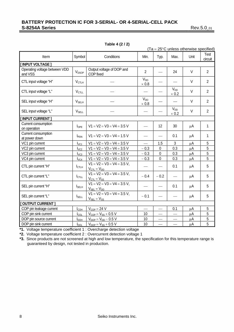
Table 4 (2 / 2)
(Ta = 25°C unless otherwise specified)
Item Symbol Conditions Min. Typ. Max. Unit Test circuit
[ INPUT VOLTAGE ] Operating voltage between VDD and VSS VDSOP Output voltage of DOP and
COP fixed 2 ⎯ 24 V 2
CTL input voltage “H” VCTLH ⎯ VDD × 0.8 ⎯ ⎯ V 2
CTL input voltage “L” VCTLL ⎯ ⎯ ⎯ VDD × 0.2 V 2
SEL input voltage “H” VSELH ⎯ VDD × 0.8 ⎯ ⎯ V 2
SEL input voltage “L” VSELL ⎯ ⎯ ⎯ VDD × 0.2 V 2
[ INPUT CURRENT ] Current consumption on operation IOPE V1 = V2 = V3 = V4 = 3.5 V ⎯ 12 30 μA 1
Current consumption at power down IPDN V1 = V2 = V3 = V4 = 1.5 V ⎯ ⎯ 0.1 μA 1
VC1 pin current IVC1 V1 = V2 = V3 = V4 = 3.5 V ⎯ 1.5 3 μA 5 VC2 pin current IVC2 V1 = V2 = V3 = V4 = 3.5 V − 0.3 0 0.3 μA 5 VC3 pin current IVC3 V1 = V2 = V3 = V4 = 3.5 V − 0.3 0 0.3 μA 5 VC4 pin current IVC4 V1 = V2 = V3 = V4 = 3.5 V − 0.3 0 0.3 μA 5
CTL pin current “H” ICTLH V1 = V2 = V3 = V4 = 3.5 V, VCTL = VDD ⎯ ⎯ 0.1 μA 5
CTL pin current “L” ICTLL V1 = V2 = V3 = V4 = 3.5 V, VCTL = VSS − 0.4 − 0.2 ⎯ μA 5
SEL pin current “H” ISELH V1 = V2 = V3 = V4 = 3.5 V, VSEL = VDD ⎯ ⎯ 0.1 μA 5
SEL pin current “L” ISELL V1 = V2 = V3 = V4 = 3.5 V, VSEL = VSS − 0.1 ⎯ ⎯ μA 5
[ OUTPUT CURRENT ] COP pin leakage current ICOH VCOP = 24 V ⎯ ⎯ 0.1 μA 5 COP pin sink current ICOL VCOP = VSS + 0.5 V 10 ⎯ ⎯ μA 5 DOP pin source current IDOH VDOP = VDD − 0.5 V 10 ⎯ ⎯ μA 5 DOP pin sink current IDOL VDOP = VSS + 0.5 V 10 ⎯ ⎯ μA 5
*1. Voltage temperature coefficient 1 : Overcharge detection voltage *2. Voltage temperature coefficient 2 : Overcurrent detection voltage 1 *3. Since products are not screened at high and low temperature, the specification for this temperature range is guaranteed by design, not tested in production.

BATTERY PROTECTION IC FOR 3-SERIAL- OR 4-SERIAL-CELL PACKRev.5.0_01 S-8254A Series
Seiko Instruments Inc. 9
Test Circuits This chapter describes how to test the S-8254A Series when a 4-serial cell is selected by setting the SEL pin to the VDD level. When a 3-serial cell is selected by setting the SEL pin to the VSS level, short the power supply V4.
1. Current Consumption on Operation, Current Consumption at Power-down
(Test circuit 1)
1.1 Current Consumption on Operation (IOPE)
The current at the VSS pin when V1 = V2 = V3 = V4 = 3.5 V and VVMP = VDD is the current consumption (IOPE) during operation.
1.2 Current Consumption at Power-down (IPDN)
The current at the VSS pin when V1 = V2 = V3 = V4 = 1.5 V and VVMP = VSS is the current consumption (IPDN) at power down.
2. Overcharge Detection Voltage, Overcharge Release Voltage, Overdischarge Detection Voltage,
Overdischarge Release Voltage, Overcurrent Detection Voltage 1, Overcurrent Detection Voltage 2, Overcurrent Detection Voltage 3, CTL Input Voltage “H”, CTL Input Voltage “L”, SEL Input Voltage “H”, SEL Input Voltage “L” (Test circuit 2)
Confirm that the COP pin and DOP pin are low (VDD × 0.1 V or lower) when VVMP = VSEL = VDD, VINI = VCTL = VSS, the CCT pin is open, the CDT pin is open, and V1 = V2 = V3 = V4 = 3.5 V (this status is referred to as the initial status).
2.1 Overcharge Detection Voltage (VCU1), Overcharge Release Voltage (VCL1)
The overcharge detection voltage (VCU1) is the voltage of V1 when the voltage of the COP pin is “H” (VDD × 0.9 V or more) after the V1 voltage has been gradually increased starting at the initial status. The overcharge release voltage (VCL1) is the voltage of V1 when the voltage at the COP pin is “L” after the V1 voltage has been gradually decreased.
2.2 Overdischarge Detection Voltage (VDL1), Overdischarge Release Voltage (VDU1)
The overdischarge detection voltage (VDL1) is the voltage of V1 when the voltage of the DOP pin is “H” after the V1 voltage has been gradually decreased starting at the initial status. The overdischarge release voltage (VDU1) is the voltage of V1 when the voltage at the DOP pin is “L” after the V1 voltage has been gradually increased. When the voltage of Vn (n = 2 to 4) is changed, the overcharge detection voltage (VCUn), overcharge release voltage (VCLn), overdischarge detection voltage (VDLn), and overdischarge release voltage (VDUn) can be determined in the same way as when n = 1.
2.3 Overcurrent Detection Voltage 1 (VIOV1)
Overcurrent detection voltage 1 (VIOV1) is the voltage of the VINI pin when the voltage of the DOP pin is “H” after the VINI pin voltage has been gradually increased starting at the initial status.
2.4 Overcurrent Detection Voltage 2 (VIOV2)
Overcurrent detection voltage 2 (VIOV2) is the voltage of the VINI pin when the voltage of the DOP pin is “H” after the voltage of the CDT pin was set to VSS following the initial status and the voltage of the VINI pin has been gradually decreased.
2.5 Overcurrent Detection Voltage 3 (VIOV3)
Overcurrent detection voltage 3 (VIOV3) is the voltage difference between VVC1 and VVMP (VVC1 − VVMP) when the voltage of the DOP pin is “H” after the VMP voltage has been gradually decreased starting at the initial status.

BATTERY PROTECTION IC FOR 3-SERIAL- OR 4-SERIAL-CELL PACK S-8254A Series Rev.5.0_01
Seiko Instruments Inc. 10
2.6 CTL Input Voltage “H” (VCTLH), CTL Input Voltage “L” (VCTLL)
The CTL input voltage “H” (VCTLH) is the voltage of CTL when the voltages at the COP and DOP pins are “H” after the CTL voltage has been gradually increased starting at the initial status. The CTL input voltage “L” (VCTLL) is the voltage of CTL when the voltages at the COP and DOP pins are “L” after the CTL voltage has been gradually decreased.
2.7 SEL Input Voltage “H” (VSELH), SEL Input Voltage “L” (VSELL)
Apply 0 V to V4 in the initial status and confirm that the DOP pin is “H”. The SEL input voltage “L” (VSELL) is the voltage of the SEL pin when the voltage at the DOP pin is “L” after the SEL voltage has been gradually decreased. The SEL input voltage “H” (VSELH) is the voltage of the SEL pin when the voltage of the DOP pin is “H” after the SEL voltage has been gradually increased.
3. Overcharge Detection Delay Time, Overdischarge Detection Delay Time, Overcurrent Detection
Delay Time 1, Overcurrent Detection Delay Time 2, Overcurrent Detection Delay Time 3 (Test circuit 3)
Confirm that the COP pin and DOP pin are “L” when VVMP = VDD, VINI = VSS, and V1 = V2 = V3 = V4 = 3.5 V (this status is referred to as the initial status).
3.1 Overcharge Detection Delay Time (tCU)
The overcharge detection delay time (tCU) is the time it takes for the voltage of the COP pin to change from “L” to “H” after the voltage of V1 is instantaneously changed to 4.5 V from the initial status.
3.2 Overdischarge Detection Delay Time (tDL)
The overdischarge detection delay time (tDL) is the time it takes for the voltage of the DOP pin to change from “L” to “H” after the voltage of V1 is instantaneously changed to 1.5 V from the initial status
3.3 Overcurrent Detection Delay Time 1 (tIOV1)
Overcurrent detection delay time 1 (tIOV1) is the time it takes for the voltage of the DOP pin to change from “L” to “H” after the voltage of the VINI pin is instantaneously changed to 0.4 V from the initial status.
3.4 Overcurrent Detection Delay Time 2 (tIOV2)
Overcurrent detection delay time 2 (tIOV2) is the time it takes for the voltage of the DOP pin to change from “L” to “H” after the voltage of the VINI pin is instantaneously changed to VIOV2 max. + 0.2 V from the initial status.
3.5 Overcurrent Detection Delay Time 3 (tIOV3)
Overcurrent detection delay time 3 (tIOV3) is the time it takes for the voltage of the DOP pin to change from “L” to “H” after the voltage of the VMP pin is instantaneously changed to VIOV3 min. − 0.2 V from the initial status.

BATTERY PROTECTION IC FOR 3-SERIAL- OR 4-SERIAL-CELL PACKRev.5.0_01 S-8254A Series
Seiko Instruments Inc. 11
4. 0 V Battery Charge Starting Charger Voltage (Product with 0 V Battery Charge Function), 0 V
Battery Charge Inhibition Battery Voltage (Product with 0 V Battery Charge Inhibition Function) (Test circuit 4)
Ether the 0 V battery charge starting charger voltage or the 0 V battery charge inhibition battery voltage is applied to each product according to the 0 V battery charging function.
4.1 0 V Battery Charge Starting Battery Charger Voltage (V0CHA) (Product with 0 V Battery Charge
Function)
The starting condition is V1 = V2 = V3 = V4 = 0 V for a product in which 0 V battery charging is available. The COP pin voltage should be lower than V0CHA max. − 1 V when the VMP pin voltage VVMP = V0CHA max.
4.2 0 V Battery Charge Inhibition Battery Voltage (V0INH) (Product with 0 V Battery Charge
Inhibition Function)
The starting condition is V1 = V2 = V3 = V4 = V0INH for a product in which 0 V battery charging is inhibited. The COP pin voltage should be higher than VVMP − 1 V when the VMP pin voltage VVMP = 24 V.
5. Resistance between VMP and VDD, Resistance between VMP and VSS, VC1 Pin Current, VC2 Pin
Current, VC3 Pin Current, VC4 Pin Current, CTL pin Current “H”, CTL Pin Current “L”, SEL Pin Current “H”, SEL Pin Current “L”, COP Pin Leakage Current, COP Pin Sink Current, DOP Pin Source Current, DOP Pin Sink Current (Test circuit 5)
VVMP = VSEL = VDD, VINI = VCTL = VSS, V1 = V2 = V3 = V4 = 3.5 V, and other pins left “open” (this status is referred to as the initial status).
5.1 Resistance between VMP and VDD (RVMD)
The resistance between VMP and VDD (RVMD) is obtained from RVMD = VDD / IVMD using the current value of the VMP pin (IVMD) when VVMP is VSS after the initial status.
5.2 Resistance between VMP and VSS (RVMS)
The resistance between VMP and VSS (RVMS) is obtained from RVMS = VDD / IVMS using the current value of the VMP pin (IVMS) when V1 = V2 = V3 = V4 = 1.8 V after the initial status.
5.3 VC1 Pin Current (IVC1), VC2 Pin Current (IVC2), VC3 Pin Current (IVC3), VC4 Pin Current (IVC4)
At the initial status, the current that flows through the VC1 pin is the VC1 pin current (IVC1), the current that flows through the VC2 pin is the VC2 pin current (IVC2), the current that flows through the VC3 pin is the VC3 pin current (IVC3), and the current that flows through the VC4 pin is the VC4 pin current (IVC4).
5.4 CTL pin Current “H” (ICTLH), CTL Pin Current “L” (ICTLL)
In the initial status, the current that flows through the CTL pin is the CTL pin current “L” (ICTLL), after that, when VCTL = VDD, the current that flows through the CTL pin is the CTL pin current “H” (ICTLH).
5.5 SEL Pin Current “H” (ISELH), SEL Pin Current “L” (ISELL)
In the initial status, the current that flows through the SEL pin is the SEL pin current “H” (ISELH), after that, when VSEL = VSS, the current that flows through the SEL pin is the SEL pin current “L” (ISELL).

BATTERY PROTECTION IC FOR 3-SERIAL- OR 4-SERIAL-CELL PACK S-8254A Series Rev.5.0_01
Seiko Instruments Inc. 12
5.6 COP Pin Leakage Current (ICOH), COP Pin Sink Current (ICOL)
The COP pin sink current (ICOL) is the current that flows through the COP pin when VCOP = VSS + 0.5 V after the initial status. After that, the current that flows through the COP pin when V1 = V2 = V3 = V4 = 6 V and VCOP = VDD is the COP pin leakage current (ICOH).
5.7 DOP Pin Source Current (IDOH), DOP Pin Sink Current (IDOL)
The DOP pin sink current (IDOL) is the current that flows through the DOP pin when VDOP = VSS + 0.5 V after the initial status. After that, the current that flows through the DOP pin when VVMP = VDD − 2 V and VDOP = VDD − 0.5 V is the DOP pin source current (IDOH).
1 COP2 VMP3 DOP4 VINI5 CDT6 CCT7 VSS8
16VDD15VC114VC213VC312VC411CTL
SELNC 9
S-8254A
C1 = 0.1 μF
NC10
V1
V2
V4
V3
A
Figure 4 Test Circuit 1
1 COP2 VMP3 DOP4 VINI5 CDT6 CCT7 VSS8
16VDD15VC114VC213VC312VC411CTL
SELNC 9
S-8254A
C1 = 0.1 μF
NC10
V1
V2
V4
V3
V V
Figure 5 Test Circuit 2

BATTERY PROTECTION IC FOR 3-SERIAL- OR 4-SERIAL-CELL PACKRev.5.0_01 S-8254A Series
Seiko Instruments Inc. 13
1 COP2 VMP3 DOP4 VINI5 CDT6 CCT7 VSS8
16VDD15VC114VC213VC312VC411CTL
SELNC 9
S-8254A
C1 = 0.1 μF
NC10
V1
V2
V4
V3
C2 = 0.1 μF
C3 = 0.1 μF
V
V
Figure 6 Test Circuit 3
1 COP2 VMP3 DOP4 VINI5 CDT6 CCT7 VSS8
16VDD15VC114VC213VC312VC411CTL
SELNC 9
S-8254A
C1 = 0.1 μF
NC10
V1
V2
V4
V3
V
Figure 7 Test Circuit 4
1 COP2 VMP3 DOP4 VINI5 CDT6 CCT7 VSS8
16VDD15VC114VC213VC312VC411CTL
SELNC 9
S-8254A
C1 = 0.1 μF
NC10
V1
V2
V4
V3
A A
A AAAAAA
Figure 8 Test Circuit 5

BATTERY PROTECTION IC FOR 3-SERIAL- OR 4-SERIAL-CELL PACK S-8254A Series Rev.5.0_01
Seiko Instruments Inc. 14
Operation
Remark Refer to “ Battery Protection IC Connection Example”.
1. Normal Status
When all of the battery voltages are in the range from VDLn to VCUn and the discharge current is lower than the specified value (the VINI pin voltage is lower than VIOV1 and VIOV2, and the VMP pin voltage is higher than VIOV3), the charging and discharging FETs are turned on.
2. Overcharge Status
When any one of the battery voltages becomes higher than VCUn and the state continues for tCU or longer, the COP pin becomes high impedance. The COP pin is pulled up to the EB+ pin voltage by an external resistor, and the charging FET is turned off to stop charging. This is called the overcharge status. The overcharge status is released when one of the following two conditions holds.
(1) All battery voltages become VCLn or lower. (2) All of the battery voltages are VCUn or lower, and the VMP pin voltage is 39 / 40 × VDD or lower (a
load is connected and discharging is started via the body diode of the charging FET).
3. Overdischarge Status
When any one of the battery voltages becomes lower than VDLn and the state continues for tDL or longer, the DOP pin voltage becomes VDD level, and the discharging FET is turned off to stop discharging. This is called the overdischarging status. After discharging is stopped due to the overdischarge status, the S-8254A Series enters the power-down status.
4. Power-down Status
When discharging has stopped due to the overdischarge status, the VMP pin is pulled down to the VSS level by the RVMS resistor. When the VMP pin voltage is lower than VDD / 2, the S-8254A Series enters the power-down status. In the power-down status, almost all the circuits of the S-8254A Series stop and the current consumption is IPDN or lower. The conditions of each output pin are as follows.
(1) COP pin : High-Z (2) DOP pin : VDD
The power-down status is released when the following condition holds.
(1) The VMP pin voltage is VDD / 2 or higher.
The following two conditions release the overdischarging status. (1) In case the VMP pin voltage is VDD / 2 or higher and the VMP pin voltage is lower than VDD, the
overdischarging status is released when all battery voltages are VDUn or higher. (2) In case a charger is connected, the overdischarge hysteresis is released. And the overdischarging
status is released when all battery voltages are VDLn or higher.

BATTERY PROTECTION IC FOR 3-SERIAL- OR 4-SERIAL-CELL PACKRev.5.0_01 S-8254A Series
Seiko Instruments Inc. 15
5. Overcurrent Status
The S-8254A Series has three overcurrent detection levels (VIOV1, VIOV2, and VIOV3) and three overcurrent detection delay times (tIOV1, tIOV2, and tIOV3) corresponding to each overcurrent detection level. When the discharging current becomes higher than the specified value (the voltage between VSS and VINI is greater than VIOV1) and the state continues for tIOV1 or longer, the S-8254A Series enters the overcurrent status, in which the DOP pin voltage becomes VDD level to turn off the discharging FET to stop discharging, the COP pin becomes high impedance and is pulled up to the EB+ pin voltage to turn off the charging FET to stop charging, and the VMP pin is pulled up to the VDD voltage by the internal resistor (RVMD). Operation of overcurrent detection level 2 (VIOV2) and overcurrent detection delay time 2 (tIOV2) is the same as for VIOV1 and tIOV1. In the overcurrent status, the VMP pin is pulled up to the VDD level by the internal resistor in the IC (RVMD resistor). The overcurrent status is released when the following condition holds.
(1) The VMP pin voltage is VIOV3 or higher because a charger is connected or the load (30 MΩ or more) is released.
6. 0 V Battery Charge Function
Regarding the charging of a self-discharged battery (0 V battery), the S-8254A Series has two functions from which one should be selected.
(1) 0 V battery charging is allowed (0 V battery charging is available.) When the charger voltage is higher than V0CHA, the 0 V battery can be charged.
(2) 0 V battery charging is prohibited (0 V battery charging is unavailable.) When one of the battery voltages is lower than V0INH, the 0 V battery cannot be charged.
Caution When the VDD pin voltage is lower than the minimum value of VDSOP, the operation of the
S-8254A Series is not guaranteed.
7. Delay Time Setting
The overcharge detection delay time (tCU) is determined by the external capacitor connected to the CCT pin. The overdischarge detection delay time (tDL) and overcurrent detection delay time 1 (tIOV1) are determined by the external capacitor connected to the CDT pin. Overcurrent detection delay times 2 and 3 (tIOV2, tIOV3) are fixed internally.
min. typ. max. tCU [s] = (5.00, 10.0, 15.0) × CCCT [μF] tDL [s] = (0.50, 1.00, 1.50) × CCDT [μF] tIOV1 [s] = (0.05, 0.10, 0.15) × CCDT [μF]
8. CTL Pin
The S-8254A Series has control pins. The CTL pin is used to control the COP and DOP pin output voltages. CTL pin takes precedence over the battery protection circuit.
Table 5 Conditions Set by CTL Pin
CTL Pin COP Pin DOP Pin High High-Z VDD Open High-Z VDD Low Normal status *1 Normal status *1
*1. The status is controlled by the voltage detector. Caution Please note unexpected behavior might occur when electrical potential difference
between the CTL pin (‘L’ level) and VSS is generated through the external filter (RVSS and CVSS) as a result of input voltage fluctuations.

BATTERY PROTECTION IC FOR 3-SERIAL- OR 4-SERIAL-CELL PACK S-8254A Series Rev.5.0_01
Seiko Instruments Inc. 16
9. SEL pin
The S-8254A Series has control pins. The SEL pin is used to switch between 3-cell and 4-cell protection. When the SEL pin is low, overdischarge detection of the V4 cell is prohibited and an overdischarge is not detected even if the V4 cell is shorted, therefore, the V4 cell can be used for 3-cell protection. The SEL pin takes precedence over the battery protection circuit. Use the SEL pin at high or low.
Table 6 Conditions Set by SEL Pin
SEL Pin Condition High 4-cell protection Open Undefined Low 3-cell protection
BATTERY PROTECTION IC FOR 3-SERIAL- OR 4-SERIAL-CELL PACKRev.5.0_01 S-8254A Series
Seiko Instruments Inc. 17
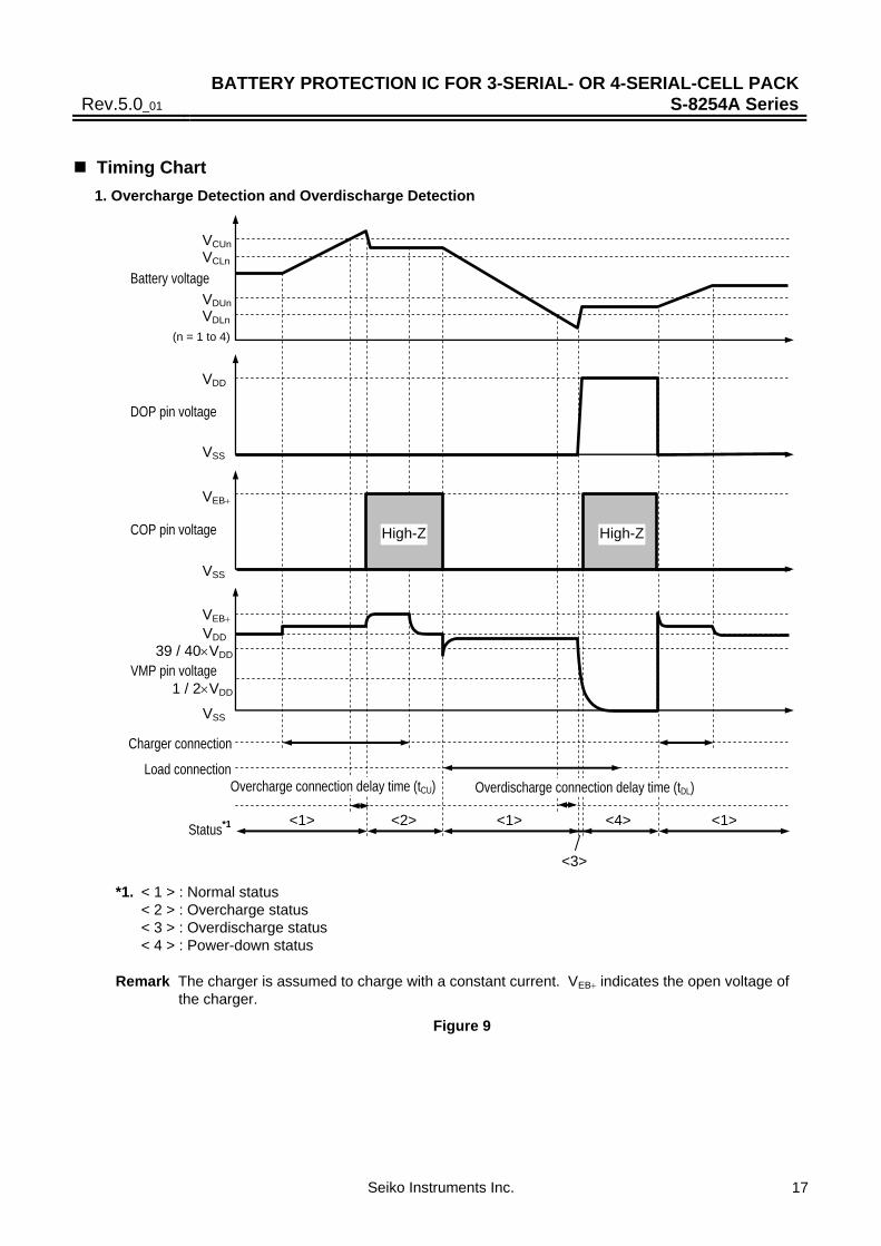
Timing Chart 1. Overcharge Detection and Overdischarge Detection
VCUn
VDUn VDLn
VCLn
High-Z
VSS
VDD
VSS
<1> <2> <1> <4> <1>
VSS
VDD
VEB+
VEB+
(n = 1 to 4)
Battery voltage
COP pin voltage
39 / 40×VDD VMP pin voltage
DOP pin voltage
Charger connection
Load connection
Status*1
Overcharge connection delay time (tCU)
High-Z
1 / 2×VDD
<3>
Overdischarge connection delay time (tDL)
*1. < 1 > : Normal status < 2 > : Overcharge status < 3 > : Overdischarge status < 4 > : Power-down status Remark The charger is assumed to charge with a constant current. VEB+ indicates the open voltage of
the charger.
Figure 9
BATTERY PROTECTION IC FOR 3-SERIAL- OR 4-SERIAL-CELL PACK S-8254A Series Rev.5.0_01
Seiko Instruments Inc. 18
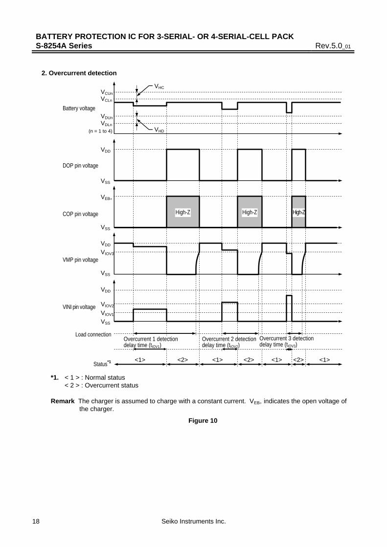
2. Overcurrent detection
VCUn
VDUn VDLn
(n = 1 to 4)
VCLn Battery voltage
VHC
VHD
VDD
DOP pin voltage
VSS
High-Z
VEB+
VSS
COP pin voltage High-Z High-Z
VDD
VSS
VMP pin voltage VIOV3
VIOV2
VSS
VINI pin voltage
VDD
VIOV1
Load connection
Status*1
Overcurrent 1 detection delay time (tIOV1)
<1> <2> <1> <1> <2> <1> <2>
Overcurrent 2 detection delay time (tIOV2)
Overcurrent 3 detection delay time (tIOV3)
*1. < 1 > : Normal status < 2 > : Overcurrent status Remark The charger is assumed to charge with a constant current. VEB+ indicates the open voltage of
the charger.
Figure 10

BATTERY PROTECTION IC FOR 3-SERIAL- OR 4-SERIAL-CELL PACKRev.5.0_01 S-8254A Series
Seiko Instruments Inc. 19
Battery Protection IC Connection Example
1. 3-serial Cell
EB+
RCOP RVMP RDOP
RVINI
CCDT
CCCT
EB−
1 COP2 VMP3 DOP4 VINI5 CDT6 CCT7 VSS8
16VDD15VC114VC213VC312VC411CTL
SELNC 9
S-8254A
RVC1
CVC2
CVC3
CVSS
CVC1
RVC2
RVC3
RCTL
RVSS
RSENSE
CTL
NC10
Charging FET
Discharging FET
RSEL
Figure 11
2. 4-serial Cell
EB+
RCOP RVMP RDOP
RVINI
CCDT
CCCT
EB−
1 COP2 VMP3 DOP4 VINI5 CDT6 CCT7 VSS8
16VDD15VC114VC213VC312VC411CTL
SELNC 9
S-8254A
RVC1
CVC2
CVC3
CVC4
CVSS
CVC1
RVC2
RVC3
RVC4
RCTL
RVSS
RSENSE
CTL
NC10
Charging FET
Discharging FET
RSEL
Figure 12
BATTERY PROTECTION IC FOR 3-SERIAL- OR 4-SERIAL-CELL PACK S-8254A Series Rev.5.0_01
Seiko Instruments Inc. 20
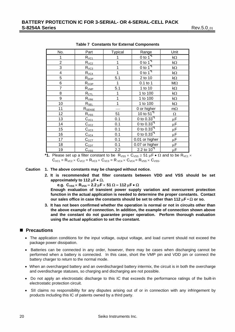
Table 7 Constants for External Components
No. Part Typical Range Unit 1 RVC1 1 0 to 1*1 kΩ 2 RVC2 1 0 to 1*1 kΩ 3 RVC3 1 0 to 1*1 kΩ 4 RVC4 1 0 to 1*1 kΩ 5 RDOP 5.1 2 to 10 kΩ 6 RCOP 1 0.1 to 1 MΩ 7 RVMP 5.1 1 to 10 kΩ 8 RCTL 1 1 to 100 kΩ 9 RVINI 1 1 to 100 kΩ
10 RSEL 1 1 to 100 kΩ 11 RSENSE ⎯ 0 or higher mΩ 12 RVSS 51 10 to 51*1 Ω 13 CVC1 0.1 0 to 0.33*1 μF 14 CVC2 0.1 0 to 0.33*1 μF 15 CVC3 0.1 0 to 0.33*1 μF 16 CVC4 0.1 0 to 0.33*1 μF 17 CCCT 0.1 0.01 or higher μF 18 CCDT 0.1 0.07 or higher μF 19 CVSS 2.2 2.2 to 10*1 μF
*1. Please set up a filter constant to be RVSS × CVSS ≥ 51 μF • Ω and to be RVC1 × CVC1 = RVC2 × CVC2 = RVC3 × CVC3 = R VC4 × CVC4 = RVSS × CVSS.
Caution 1. The above constants may be changed without notice. 2. It is recommended that filter constants between VDD and VSS should be set
approximately to 112 μF • Ω. e.g. CVSS × RVSS = 2.2 μF × 51 Ω = 112 μF • Ω
Enough evaluation of transient power supply variation and overcurrent protection function in the actual application is needed to determine the proper constants. Contact our sales office in case the constants should be set to other than 112 μF • Ω or so.
3. It has not been confirmed whether the operation is normal or not in circuits other than the above example of connection. In addition, the example of connection shown above and the constant do not guarantee proper operation. Perform thorough evaluation using the actual application to set the constant.
Precautions
• The application conditions for the input voltage, output voltage, and load current should not exceed the package power dissipation.
• Batteries can be connected in any order, however, there may be cases when discharging cannot be performed when a battery is connected. In this case, short the VMP pin and VDD pin or connect the battery charger to return to the normal mode.
• When an overcharged battery and an overdischarged battery intermix, the circuit is in both the overcharge and overdischarge statuses, so charging and discharging are not possible.
• Do not apply an electrostatic discharge to this IC that exceeds the performance ratings of the built-in electrostatic protection circuit.
• SII claims no responsibility for any disputes arising out of or in connection with any infringement by products including this IC of patents owned by a third party.
BATTERY PROTECTION IC FOR 3-SERIAL- OR 4-SERIAL-CELL PACKRev.5.0_01 S-8254A Series
Seiko Instruments Inc. 21
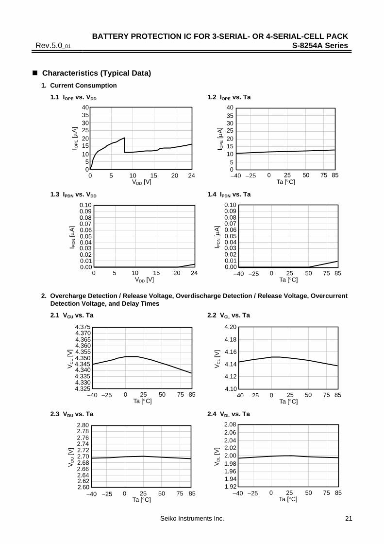
Characteristics (Typical Data) 1. Current Consumption
1.1 IOPE vs. VDD 1.2 IOPE vs. Ta
0 5 10 15 20 24
5 0
10 15 20 25 30 35 40
I OPE
[μA
]
VDD [V]
−40 −25 0 25 50 75 85
50
10152025303540
I OPE
[μA
]
Ta [°C] 1.3 IPDN vs. VDD 1.4 IPDN vs. Ta
0 5 10 15 20 24
0.01 0.00
0.020.03 0.04 0.05 0.06 0.07 0.08 0.09 0.10
I PD
N [μ
A]
VDD [V]
−40 −25 0 25 50 75 85
0.010.00
0.020.030.040.050.060.070.080.090.10
I PD
N [μ
A]
Ta [°C]
2. Overcharge Detection / Release Voltage, Overdischarge Detection / Release Voltage, Overcurrent Detection Voltage, and Delay Times
2.1 VCU vs. Ta 2.2 VCL vs. Ta
−40 −25 0 25 50 75 85
4.330 4.325
4.335 4.340 4.345 4.350 4.355 4.360 4.365 4.370 4.375
VC
U [V
]
Ta [°C]
−40 −25 0 25 50 75 854.10
4.12
4.14
4.16
4.18
4.20
V CL [
V]
Ta [°C] 2.3 VDU vs. Ta 2.4 VDL vs. Ta
−40 −25 0 25 50 75 85
2.62 2.60
2.64 2.66 2.68 2.70 2.72 2.74 2.76 2.78 2.80
V DU [V
]
Ta [°C]
−40 −25 0 25 50 75 85
1.941.92
1.961.982.002.022.042.062.08
V DL [
V]
Ta [°C]

BATTERY PROTECTION IC FOR 3-SERIAL- OR 4-SERIAL-CELL PACK S-8254A Series Rev.5.0_01
Seiko Instruments Inc. 22
2.5 VIOV1 vs. VDD 2.6 VIOV1 vs. Ta
10 11 12 13 14 15 16
0.26 0.25
0.27 0.28 0.29 0.30 0.31 0.32 0.33 0.34 0.35
V IO
V1 [
V]
VDD [V]
−40 −25 0 25 50 75 85
0.2800.275
0.2850.2900.2950.3000.3050.3100.3150.3200.325
VIO
V1 [V
]
Ta [°C] 2.7 VIOV2 vs. VDD 2.8 VIOV2 vs. Ta
10 11 12 13 14 15 16
0.42 0.40
0.440.46 0.48 0.50 0.52 0.54 0.56 0.58 0.60
V IO
V2 [
V]
VDD [V]
−40 −25 0 25 50 75 85
0.420.40
0.440.460.480.500.520.540.560.580.60
V IO
V2 [V
]
Ta [°C] 2.9 VIOV3 vs. VDD 2.10 VIOV3 vs. Ta
10 11 12 13 14 15 16
−1.4
−1.5
−1.3
−1.2
−1.1
−0.9 −1.0
V IO
V3 [
V]
VDD [V] −40 −25 0 25 50 75 85
−1.4
−1.5
−1.3
−1.2
−1.1
−0.9−1.0
VIO
V3 [
V]
Ta [°C] 2.11 tCU vs. CCCT 2.12 tCU vs. Ta
0.01 10.01
100
10
1
0.1
0.1
t CU [s
]
CCCT [μF]
−40 0 50 85
0.8
0.6
1.0
1.2
1.4
7525 −25
t CU [s
]
Ta [°C]
BATTERY PROTECTION IC FOR 3-SERIAL- OR 4-SERIAL-CELL PACKRev.5.0_01 S-8254A Series
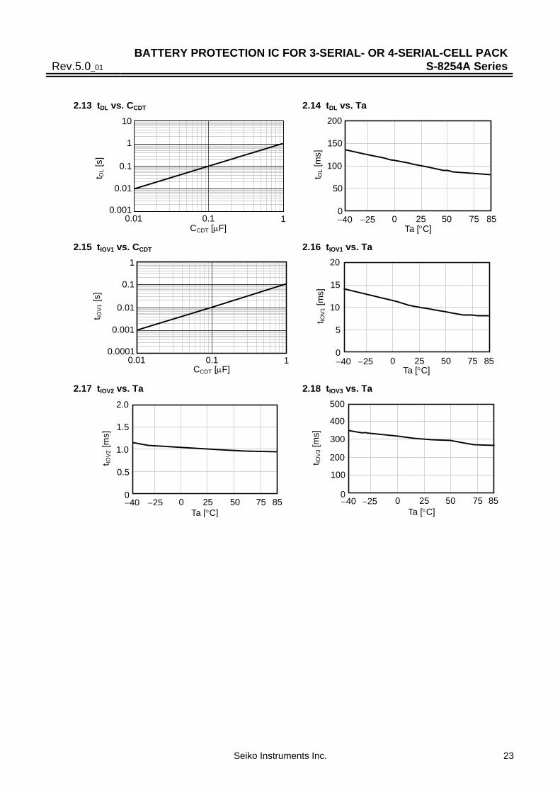
Seiko Instruments Inc. 23
2.13 tDL vs. CCDT 2.14 tDL vs. Ta
0.001
10
1
0.1
0.01
0.01 10.1
t DL [
s]
CCDT [μF]
−40 0 50 85
50
0
100
150
200
−25 25 75
t DL [
ms]
Ta [°C] 2.15 tIOV1 vs. CCDT 2.16 tIOV1 vs. Ta
0.0001
1
0.1
0.01
0.001
0.01 10.1
t IOV1
[s]
CCDT [μF]
−40 0 50 85
5
0
10
15
20
25 −25 75
t IOV1
[ms]
Ta [°C] 2.17 tIOV2 vs. Ta 2.18 tIOV3 vs. Ta
−40 0 50 85
0.5
0
1.0
1.5
2.0
7525 −25
t IOV
2 [m
s]
Ta [°C]
−40 0 50 85
100
0
200
300
500
400
7525 −25
t IOV
3 [m
s]
Ta [°C]

BATTERY PROTECTION IC FOR 3-SERIAL- OR 4-SERIAL-CELL PACK S-8254A Series Rev.5.0_01
Seiko Instruments Inc. 24
3. COP / DOP Pin
3.1 ICOH vs. VCOP 3.2 ICOL vs. VCOP
0 5 10 15 20 24
0.02
0
0.03 0.04
0.06 0.07 0.08
0.10
0.05
0.01
0.09
I CO
H [μ
A]
VCOP [V]
0 7 10.5 14
5
0
10
15
25
20
3.5
I CO
L [m
A]
VCOP [V] 3.3 IDOH vs. VDOP 3.4 IDOL vs. VDOP
0 1.8 3.6 5.4 7.2
−4.0
−5.0
−3.5 −3.0
−2.0 −1.5 −1.0
0
−2.5
−4.5
−0.5
I DO
H [m
A]
VDOP [V]
0 3.5 10.5 14
5
0
10
15
20
25
7
I DO
L [m
A]
VDOP [V]

���������
�
�
�
�������
�����������
� �
�����
�����
���� ��
���� � ������������ �� �
� ��!���"�"#"�$"���
!���"�"#"�$"���
���%#�"�"#&'�$������ ��

(������
�������)���
*����"�
)������
������
(������
��*��(�"���
��+�����
�������
,���-
� �
�����
�����
���� ��
�
�
�
���� � ������������ �� �
� ��!���"�"�"�$"���
!���"�"�"�$"���
���%#�"�"�.�� �� � � �./�
!��0�0��� �� �

� �
�����
�����
���� ��
���(����
���� � ������������ �� �
� ��!���"�"1"�$"���
!���"�"1"�$"���
���%#�"�" � 1��2
3�4� �5���
��2.�6�0�0�.7��6�����8�� ����.2�/.��
�����
)�+����)�����
���(����
���(*����"���
� �
�����
�����
���� ��
���(����
���� � ������������ �� �
� ��!���"�"1"��"���
!���"�"1"��"���
���%#�"�" � 1��2
3�4� (5���
��2.�6�0�0�.7��6�����8�� ����.2�/.��
�����
)�+����)�����
���(����
���(*����"���

www.sii-ic.com
• The information described herein is subject to change without notice.
• Seiko Instruments Inc. is not responsible for any problems caused by circuits or diagrams described hereinwhose related industrial properties, patents, or other rights belong to third parties. The application circuit examples explain typical applications of the products, and do not guarantee the success of any specific mass-production design.
• When the products described herein are regulated products subject to the Wassenaar Arrangement or other agreements, they may not be exported without authorization from the appropriate governmental authority.
• Use of the information described herein for other purposes and/or reproduction or copying without theexpress permission of Seiko Instruments Inc. is strictly prohibited.
• The products described herein cannot be used as part of any device or equipment affecting the humanbody, such as exercise equipment, medical equipment, security systems, gas equipment, or any apparatus installed in airplanes and other vehicles, without prior written permission of Seiko Instruments Inc.
• The products described herein are not designed to be radiation-proof.
• Although Seiko Instruments Inc. exerts the greatest possible effort to ensure high quality and reliability, thefailure or malfunction of semiconductor products may occur. The user of these products should thereforegive thorough consideration to safety design, including redundancy, fire-prevention measures, andmalfunction prevention, to prevent any accidents, fires, or community damage that may ensue.