RX71M Group Datasheet · 2019-10-12 · RX71M Group 1. Overview R01DS0249EJ0100 Rev.1.00 Page 4 of...
228
RX71M Group Renesas MCUs Datasheet R01DS0249EJ0100 Rev.1.00 Page 1 of 228 Jan 15, 2015 Features ■ 32-bit RXv2 CPU core Max. operating frequency: 240 MHz Capable of 480 DMIPS in operation at 240 MHz Single precision 32-bit IEEE-754 floating point Two types of multiply-and-accumulation unit (between memories and between registers) 32-bit multiplier (fastest instruction execution takes one CPU clock cycle) Divider (fastest instruction execution takes two CPU clock cycles) Fast interrupt CISC Harvard architecture with 5-stage pipeline Variable-length instructions: Ultra-compact code Supports the memory protection unit (MPU) JTAG and FINE (one-line) debugging interfaces ■ Low-power design and architecture Operation from a single 2.7- to 3.6-V supply Low power consumption: A product that supports all peripheral functions draws only 0.2mA/MHz (Typ.). RTC is capable of operation from a dedicated power supply. Four low-power modes ■ On-chip code flash memory Supports versions with up to 4 Mbytes of ROM No wait states at up to 120 MHz or when the AFU is hit, one wait state at above 120 MHz and when the AFU is missed User code is programmable by on-board or off-board programming. Programming/erasing as background operations (BGOs) ■ On-chip data flash memory 64 Kbytes, reprogrammable up to 100,000 times Programming/erasing as background operations (BGOs) ■ On-chip SRAM 512 Kbytes of SRAM (no wait states except in the 256 Kbytes from 0004 0000h to 0007 FFFFh when ICLK is set to 120 MHz or faster) 32 Kbytes of RAM with ECC (single-error correction and double error detection) 8 Kbytes of standby RAM (backup on deep software standby) ■ Data transfer DMAC: 8 channels DTC EXDMAC: 2 channels DMAC for the Ethernet controller: 3 channels for 176- and 177-pin products; 2 channels for 100-, 144-, and 145-pin products ■ Reset and supply management Power-on reset (POR) Low voltage detection (LVD) with voltage settings ■ Clock functions External crystal oscillator or internal PLL for operation at 8 to 24 MHz Internal 240-kHz LOCO and HOCO selectable from 16, 18, and 20 MHz 120-kHz clock for the IWDTa ■ Real-time clock Adjustment functions (30 seconds, leap year, and error) Real-time clock counting and binary counting modes are selectable Time capture function (for capturing times in response to event-signal input) ■ Independent watchdog timer 120-kHz (1/2 LOCO frequency) clock operation ■ Useful functions for IEC60730 compliance Oscillation-stoppage detection, frequency measurement, CRC, IWDTa, self-diagnostic function for the A/D converter, etc. Register write protection function can protect values in important registers against overwriting. ■ Various communications interfaces IEEE 1588-compliant Ethernet MAC (for 176- and 177-pin products: 2 modules) PHY layer for host/function or OTG controller (1) with high-speed USB 2.0 with battery charging transfer (only for 176- and 177-pin products) PHY layer (1) for host/function or OTG controller (1) with full- speed USB 2.0 transfer CAN (compliant with ISO11898-1), incorporating 32 mailboxes (up to 3 modules) SCIg and SCIh with multiple functionalities (up to 9) Choose from among asynchronous mode, clock-synchronous mode, smart-card interface mode, simplified SPI, simplified I 2 C, and extended serial mode. SCIFA with 16-byte transmission and reception FIFOs (up to 4 interfaces) I 2 C bus interface for transfer at up to 1 Mbps (up to 2 interfaces) Four-wire QSPI (1 interface) in addition to RSPIa (2 interfaces) Parallel data capture unit (PDC) for the CMOS camera interface (not in 100-pin products) SD host interface (optional: 1 interface) with a 1- or 4-bit SD bus for use with SD memory or SDIO MMCIF with 1-, 4-, or 8-bit transfer bus width ■ External address space Buses for full-speed data transfer (max. operating frequency of 60 MHz) 8 CS areas 8-, 16-, or 32-bit bus space is selectable per area Independent SDRAM area (128 Mbytes) ■ Up to 29 extended-function timers 16-bit TPUa, MTU3a, and GPTa: input capture, output compare, PWM waveform output 8-bit TMRa (4 channels), 16-bit CMT (4 channels), 32-bit CMTW (2 channels) ■ 12-bit A/D converter Two 12-bit units (8 channels for unit 0; 21 channels for unit 1) Self diagnosis Detection of analog input disconnection ■ 12-bit D/A converter: 2 channels On-chip operational amplifier output or direct input selectable ■ Temperature sensor for measuring temperature within the chip ■ Encryption (optional) AES (key lengths: 128, 196, and 256 bits) DES (key lengths: 56 bits (DES); 3 × 56 bits (T-DES)) SHA (SHA-1 (128), SHA-2 (224 or 256), HMAC (160, 224, or 256)) ■ Up to 127 pins for general I/O ports 5-V tolerance, open drain, input pull-up, switchable driving ability ■ Operating temp. range –40C to +85C PLQP0176KB-A 24 × 24 mm, 0.5-mm pitch PLQP0144KA-A 20 × 20 mm, 0.5-mm pitch PLQP0100KB-A 14 × 14 mm, 0.5-mm pitch PTLG0177KA-A 8 × 8 mm, 0.5-mm pitch PTLG0145KA-A 7 × 7 mm, 0.5-mm pitch PTLG0100JA-A 7 × 7 mm, 0.65-mm pitch PLBG0176GA-A 13 × 13mm, 0.8-mm pitch 240-MHz 32-bit RX MCU, on-chip FPU, 480 DMIPS, up to 4-MB flash memory, 512-KB SRAM, various communications interfaces including IEEE 1588-compliant Ethernet MAC, high-speed USB 2.0 with battery charging, SD host interface (optional), quad SPI, and CAN, 12-bit A/D converter, RTC, encryption (optional), serial interface for audio, CMOS camera interface R01DS0249EJ0100 Rev.1.00 Jan 15, 2015 Features
Transcript of RX71M Group Datasheet · 2019-10-12 · RX71M Group 1. Overview R01DS0249EJ0100 Rev.1.00 Page 4 of...

RX71M GroupRenesas MCUs
Datasheet
R01DS0249EJ0100 Rev.1.00 Page 1 of 228Jan 15, 2015
Features 32-bit RXv2 CPU core Max. operating frequency: 240 MHz
Capable of 480 DMIPS in operation at 240 MHz Single precision 32-bit IEEE-754 floating point Two types of multiply-and-accumulation unit (between memories
and between registers) 32-bit multiplier (fastest instruction execution takes one CPU clock
cycle) Divider (fastest instruction execution takes two CPU clock cycles) Fast interrupt CISC Harvard architecture with 5-stage pipeline Variable-length instructions: Ultra-compact code Supports the memory protection unit (MPU) JTAG and FINE (one-line) debugging interfaces
Low-power design and architecture Operation from a single 2.7- to 3.6-V supply Low power consumption: A product that supports all peripheral
functions draws only 0.2mA/MHz (Typ.). RTC is capable of operation from a dedicated power supply. Four low-power modes
On-chip code flash memory Supports versions with up to 4 Mbytes of ROM No wait states at up to 120 MHz or when the AFU is hit, one wait
state at above 120 MHz and when the AFU is missed User code is programmable by on-board or off-board programming. Programming/erasing as background operations (BGOs)
On-chip data flash memory 64 Kbytes, reprogrammable up to 100,000 times Programming/erasing as background operations (BGOs)
On-chip SRAM 512 Kbytes of SRAM (no wait states except in the 256 Kbytes from
0004 0000h to 0007 FFFFh when ICLK is set to 120 MHz or faster) 32 Kbytes of RAM with ECC (single-error correction and double
error detection) 8 Kbytes of standby RAM (backup on deep software standby)
Data transfer DMAC: 8 channels DTC EXDMAC: 2 channels DMAC for the Ethernet controller: 3 channels for 176- and 177-pin
products; 2 channels for 100-, 144-, and 145-pin products
Reset and supply management Power-on reset (POR) Low voltage detection (LVD) with voltage settings
Clock functions External crystal oscillator or internal PLL for operation at 8 to 24
MHz Internal 240-kHz LOCO and HOCO selectable from 16, 18, and 20
MHz 120-kHz clock for the IWDTa
Real-time clock Adjustment functions (30 seconds, leap year, and error) Real-time clock counting and binary counting modes are selectable Time capture function
(for capturing times in response to event-signal input)
Independent watchdog timer 120-kHz (1/2 LOCO frequency) clock operation
Useful functions for IEC60730 compliance Oscillation-stoppage detection, frequency measurement, CRC,
IWDTa, self-diagnostic function for the A/D converter, etc. Register write protection function can protect values in important
registers against overwriting.
Various communications interfaces IEEE 1588-compliant Ethernet MAC
(for 176- and 177-pin products: 2 modules) PHY layer for host/function or OTG controller (1) with high-speed
USB 2.0 with battery charging transfer (only for 176- and 177-pin products)
PHY layer (1) for host/function or OTG controller (1) with full-speed USB 2.0 transfer
CAN (compliant with ISO11898-1), incorporating 32 mailboxes (up to 3 modules)
SCIg and SCIh with multiple functionalities (up to 9)Choose from among asynchronous mode, clock-synchronous mode, smart-card interface mode, simplified SPI, simplified I2C, and extended serial mode.
SCIFA with 16-byte transmission and reception FIFOs (up to 4 interfaces)
I2C bus interface for transfer at up to 1 Mbps (up to 2 interfaces) Four-wire QSPI (1 interface) in addition to RSPIa (2 interfaces) Parallel data capture unit (PDC) for the CMOS camera interface (not
in 100-pin products) SD host interface (optional: 1 interface) with a 1- or 4-bit SD bus for
use with SD memory or SDIO MMCIF with 1-, 4-, or 8-bit transfer bus width
External address space Buses for full-speed data transfer (max. operating frequency of 60
MHz) 8 CS areas 8-, 16-, or 32-bit bus space is selectable per area Independent SDRAM area (128 Mbytes)
Up to 29 extended-function timers 16-bit TPUa, MTU3a, and GPTa: input capture, output compare,
PWM waveform output 8-bit TMRa (4 channels), 16-bit CMT (4 channels), 32-bit CMTW (2
channels)
12-bit A/D converter Two 12-bit units (8 channels for unit 0; 21 channels for unit 1) Self diagnosis Detection of analog input disconnection
12-bit D/A converter: 2 channels On-chip operational amplifier output or direct input selectable
Temperature sensor for measuring temperature within the chip
Encryption (optional) AES (key lengths: 128, 196, and 256 bits) DES (key lengths: 56 bits (DES); 3 × 56 bits (T-DES)) SHA (SHA-1 (128), SHA-2 (224 or 256), HMAC (160, 224, or 256))
Up to 127 pins for general I/O ports 5-V tolerance, open drain, input pull-up, switchable driving ability
Operating temp. range –40C to +85C
PLQP0176KB-A 24 × 24 mm, 0.5-mm pitchPLQP0144KA-A 20 × 20 mm, 0.5-mm pitchPLQP0100KB-A 14 × 14 mm, 0.5-mm pitch
PTLG0177KA-A 8 × 8 mm, 0.5-mm pitchPTLG0145KA-A 7 × 7 mm, 0.5-mm pitchPTLG0100JA-A 7 × 7 mm, 0.65-mm pitch
PLBG0176GA-A 13 × 13mm, 0.8-mm pitch
240-MHz 32-bit RX MCU, on-chip FPU, 480 DMIPS, up to 4-MB flash memory, 512-KB SRAM, various communications interfaces including IEEE 1588-compliant Ethernet MAC, high-speed USB 2.0 with battery charging, SD host interface (optional), quad SPI, and CAN, 12-bit A/D converter, RTC, encryption (optional), serial interface for audio, CMOS camera interface
R01DS0249EJ0100Rev.1.00
Jan 15, 2015
Features

RX71M Group 1. Overview
R01DS0249EJ0100 Rev.1.00 Page 2 of 228Jan 15, 2015
1. Overview
1.1 Outline of Specifications
Table 1.1 lists the specifications in outline, and Table 1.2 gives a comparison of the functions of products in different
packages.
Table 1.1 shows the outline of maximum specifications, and the number of peripheral module channels differs
depending on the pin number on the package and the code flash memory capacity. For details, see Table 1.2,
Comparison of Functions for Different Packages.
Table 1.1 Outline of Specifications (1/10)
Classification Module/Function Description
CPU CPU Maximum operating frequency: 240 MHz 32-bit RX CPU (RXv2) Minimum instruction execution time: One instruction per state (cycle of the system
clock) Address space: 4-Gbyte linear Register set of the CPU
General purpose: Sixteen 32-bit registersControl: Ten 32-bit registersAccumulator: Two 72-bit registers
Basic instructions: 75 Floating-point instructions: 11 DSP instructions: 23 Addressing modes: 11 Data arrangement
Instructions: Little endianData: Selectable as little endian or big endian
On-chip 32-bit multiplier: 32 × 32 → 64 bits On-chip divider: 32 / 32 → 32 bits Barrel shifter: 32 bits
FPU Single precision (32-bit) floating point Data types and floating-point exceptions in conformance with the IEEE754 standard
Memory Code flash memory Capacity: 2 Mbytes, 2.5 Mbytes, 3 Mbytes, 4 Mbytes No-wait access at up to 120 MHz, single wait access at frequencies above 120 MHz No-wait access to instructions and operands when the AFU is hit in operation at 240
MHz On-board programming: Four types Off-board programming (parallel programmer mode) The trusted memory (TM) function protects against the reading of programs from blocks
8 and 9.
Data flash memory Capacity: 64 Kbytes Programming/erasing: 100,000 times
RAM Capacity: 512 Kbytes 0000 0000h to 0003 FFFFh (256 Kbytes): 240 MHz No-wait access
0004 0000h to 0007 FFFFh (256 Kbytes): No-wait access at up to 120 MHz, single wait access at frequencies above 120 MHz
RAM with ECC Capacity: 32 Kbytes Single wait access at up to 120 MHz, two wait accesses for reading and three wait
accesses for writing at frequencies above 120 MHz SEC-DED (single error correction/double error detection)
Standby RAM Capacity: 8 Kbytes Operation synchronized with PCLKB: Up to 60 MHz, two-cycle access

RX71M Group 1. Overview
R01DS0249EJ0100 Rev.1.00 Page 3 of 228Jan 15, 2015
Operating modes Operating modes by the mode-setting pins at the time of release from the reset stateSingle-chip modeBoot mode (for the SCI interface)Boot mode (for the USB interface)User boot mode
Selection of operating mode by register settingSingle-chip mode, user boot modeOn-chip ROM disabled extended modeOn-chip ROM enabled extended mode
Endian selectable
Clock Clock generation circuit Main clock oscillator, sub clock oscillator, low-speed/high-speed on-chip oscillator, PLL frequency synthesizer, and IWDT-dedicated on-chip oscillator
The peripheral module clocks can be set to frequencies above that of the system clock. Main-clock oscillation stoppage detection Separate frequency-division and multiplication settings for the system clock (ICLK),
peripheral module clocks (PCLKA, PCLKB, PCLKC, PCLKD), flash-IF clock (FCLK) and external bus clock (BCLK)The CPU and other bus masters run in synchronization with the system clock (ICLK): Up to 240 MHzPeripheral modules of MTU3, GPT, RSPI, SCIFA, USBA, ETHERC, EPTPC, EDMAC, and AES run in synchronization with PCLKA, which operates at up to 120 MHz.Other peripheral modules run in synchronization with PCLKB: Up to 60 MHzADCLK in the SD12AD (unit 0) runs in synchronization with PCLKC: Up to 60 MHzADCLK in the SD12AD (unit 1) runs in synchronization with PCLKD: Up to 60 MHzFlash IF run in synchronization with the flash-IF clock (FCLK): Up to 60 MHzDevices connected to the external bus run in synchronization with the external bus clock (BCLK): Up to 60 MHz
Multiplication is possible with using the high-speed on-chip oscillator (HOCO) as a reference clock of the PLL circuit
Reset Nine types of reset RES# pin reset: Generated when the RES# pin is driven low. Power-on reset: Generated when the RES# pin is driven high and VCC = AVCC0 =
AVCC1 rises. Voltage-monitoring 0 reset: Generated when VCC = AVCC0 = AVCC1 falls. Voltage-monitoring 1 reset: Generated when VCC = AVCC0 = AVCC1 falls. Voltage-monitoring 2 reset: Generated when VCC = AVCC0 = AVCC1 falls. Deep software standby reset: Generated in response to an interrupt to trigger release
from deep software standby. Independent watchdog timer reset: Generated when the independent watchdog timer
underflows, or a refresh error occurs. Watchdog timer reset: Generated when the watchdog timer underflows, or a refresh
error occurs. Software reset: Generated by register setting.
Power-on reset If the RES# pin is at the high level when power is supplied, an internal reset is generated.After VCC = AVCC0 = AVCC1 has exceeded the voltage detection level and the specified period has elapsed, the reset is cancelled.
Voltage detection circuit (LVDA) Monitors the voltage being input to the VCC = AVCC0 = AVCC1 pins and generates an internal reset or internal interrupt. Voltage detection circuit 0
Capable of generating an internal resetThe option-setting memory can be used to select enabling or disabling of the reset.Voltage detection level: Selectable from three different levels (2.94 V, 2.87 V, and 2.80 V)
Voltage detection circuits 1 and 2Voltage detection level: Selectable from three different levels (2.99 V, 2.92 V, and 2.85 V)Digital filtering (1/2, 1/4, 1/8, and 1/16 LOCO frequency)Capable of generating an internal reset
Two types of timing are selectable for release from resetAn internal interrupt can be requested.
Detection of voltage rising above and falling below thresholds is selectable. Maskable or non-maskable interrupt is selectable
Voltage detection monitoringEvent linking
Table 1.1 Outline of Specifications (2/10)
Classification Module/Function Description

RX71M Group 1. Overview
R01DS0249EJ0100 Rev.1.00 Page 4 of 228Jan 15, 2015
Low power consumption
Low power consumption facilities
Module stop function Four low power consumption modes
Sleep mode, all-module clock stop mode, software standby mode, and deep software standby mode
Battery backup function When the voltage on the VCC pin drops, battery power from the VBATT pin is supplied to keep the real-time clock (RTC) operating.
Interrupt Interrupt controller(ICUA)
Peripheral function interrupts: 298 sources External interrupts: 16 (pins IRQ0 to IRQ15) Software interrupts: 2 sources Non-maskable interrupts: 7 sources Sixteen levels specifiable for the order of priority Method of interrupt source selection:
The interrupt vectors consist of 256 vectors (128 sources are fixed. The remaining 128 vectors are selected from among the other 157 sources.)
External bus extension The external address space can be divided into eight areas (CS0 to CS7), each with independent control of access settings.Capacity of each area: 16 Mbytes (CS0 to CS7)A chip-select signal (CS0# to CS7#) can be output for each area.Each area is specifiable as an 8-, 16-, or 32-bit bus space.The data arrangement in each area is selectable as little or big endian (only for data).
SDRAM interface connectable Bus format: Separate bus, multiplex bus Wait control Write buffer facility
DMA DMA controller(DMACAa)
8 channels Three transfer modes: Normal transfer, repeat transfer, and block transfer Activation sources: Software trigger, external interrupts, and interrupt requests from
peripheral functions
EXDMA controller (EXDMACa)
2 channelsFour transfer modes: Normal transfer, repeat transfer, block transfer, and cluster transfer
Single-address transfer enabled with the EDACKn signal Activation sources: Software trigger, external DMA requests (EDREQn), and interrupt
requests from peripheral functions
Data transfer controller (DTCa)
Three transfer modes: Normal transfer, repeat transfer, and block transfer Activation sources: External interrupts and interrupt requests from peripheral functions
I/O ports Programmable I/O ports I/O ports for the 177-pin TFLGA (in planning), 176-pin LFBGA (in planning), and 176-pin LQFPI/O pins: 127Input pin: 1Pull-up resistors: 127Open-drain outputs: 1275-V tolerance: 19
I/O ports for the 145-pin TFLGA (in planning) and 144-pin LQFPI/O pins: 111Input pin: 1Pull-up resistors: 111Open-drain outputs: 1115-V tolerance: 18
I/O ports for the 100-pin TFLGA (in planning) and 100-pin LQFPI/O pins: 78Input pin: 1Pull-up resistors: 78Open-drain outputs: 785-V tolerance: 17
Table 1.1 Outline of Specifications (3/10)
Classification Module/Function Description

RX71M Group 1. Overview
R01DS0249EJ0100 Rev.1.00 Page 5 of 228Jan 15, 2015
Event link controller (ELC) Event signals such as interrupt request signals can be interlinked with the operation of functions such as timer counting, eliminating the need for intervention by the CPU to control the functions.
119 internal event signals can be freely combined for interlinked operation with connected functions.
Event signals from peripheral modules can be used to change the states of output pins (of ports B and E).
Changes in the states of pins (of ports B and E) being used as inputs can be interlinked with the operation of peripheral modules.
Timers 16-bit timer pulse unit (TPUa)
(16 bits × 6 channels) × 1 unit Maximum of 16 pulse-input/output possible Select from among seven or eight counter-input clock signals for each channel Input capture/output compare function Output of PWM waveforms in up to 15 phases in PWM mode Support for buffered operation, phase-counting mode (two phase encoder input) and
cascade-connected operation (32 bits × 2 channels) depending on the channel. PPG output trigger can be generated Capable of generating conversion start triggers for the A/D converters Digital filtering of signals from the input capture pins Event linking by the ELC
Timers Multifunction timer pulse unit (MTU3a)
9 channels (16 bits × 8 channels, 32 bits × 1 channel) Maximum of 16 pulse-input/output and 3 pulse-input possible Select from among 13 counter-input clock signals for each channel (PCLKA/1, PCLKA/
2, PCLKA/4, PCLKA/8, PCLKA/16, PCLK/A32, PCLKA/64, PCLKA/256, PCLKA/1024, MTCLKA, MTCLKB, MTCLKC, MTCLKD) 11 of the signals are available for channels 1, 3 and 4, 12 are available for channel 2, and 9 are available for channels 5 to 8.
Input capture function 39 output compare/input capture registers Counter clear operation (synchronous clearing by compare match/input capture) Simultaneous writing to multiple timer counters (TCNT) Simultaneous register input/output by synchronous counter operation Buffered operation Support for cascade-connected operation 43 interrupt sources Automatic transfer of register data Pulse output mode
Toggle/PWM/complementary PWM/reset-synchronized PWM Complementary PWM output mode
Outputs non-overlapping waveforms for controlling 3-phase invertersAutomatic specification of dead timesPWM duty cycle: Selectable as any value from 0% to 100%Delay can be applied to requests for A/D conversion.Non-generation of interrupt requests at peak or trough values of counters can be selected.Double buffer configuration
Reset synchronous PWM modeThree phases of positive and negative PWM waveforms can be output with desired duty cycles.
Phase-counting mode: 16-bit mode (channels 1 and 2); 32-bit mode (channels 1 and 2) Counter functionality for dead-time compensation Generation of triggers for A/D converter conversion A/D converter start triggers can be skipped Digital filter function for signals on the input capture and external counter clock pins PPG output trigger can be generated Event linking by the ELC
Port output enable 3 (POE3a)
Control of the high-impedance state of the MTU3/GPT's waveform output pins 5 pins for input from signal sources: POE0, POE4, POE8, POE10, POE11 Initiation on detection of short-circuited outputs (detection of simultaneous PWM output
to the active level) Initiation by oscillation-stoppage detection or software Additional programming of output control target pins is enabled
Table 1.1 Outline of Specifications (4/10)
Classification Module/Function Description

RX71M Group 1. Overview
R01DS0249EJ0100 Rev.1.00 Page 6 of 228Jan 15, 2015
Timers General PWM timer (GPTa)
16 bits × 4 channels Counting up or down (saw-wave), counting up and down (triangle-wave) selectable for
all channels Four clock sources independently selectable for all channels (PCLKA/1, PCLKA/4,
PCLKA/8, PCLKA/16) 2 input/output pins per channel 2 output compare/input capture registers per channel For the 2 output compare/input capture registers of each channel, 4 registers are
provided as buffer registers and are capable of operating as comparison registers when buffering is not in use.
In output compare operation, buffer switching can be at peaks or troughs, enabling the generation of laterally asymmetrically PWM waveforms.
Registers for setting up frame intervals on each channel (with capability for generating interrupts on overflow or underflow)
Synchronizable operation of the several counters Modes of synchronized operation (synchronized, or displaced by desired times for
phase shifting) Generation of dead times in PWM operation Through combination of three counters, generation of automatic three-phase PWM
waveforms incorporating dead times Starting, clearing, and stopping counters in response to external or internal triggers Internal trigger sources: output of the internal comparator detection, software, and
compare-match Digital filter function for signals on the input capture and external trigger pins Event linking by the ELC
Programmable pulse generator (PPG)
(4 bits × 4 groups) × 2 units Pulse output with the MTU or TPU output as a trigger Maximum of 32 pulse-output possible
8-bit timers (TMRb) (8 bits × 2 channels) × 2 units Select from among seven internal clock signals (PCLKB/1, PCLKB/2, PCLKB/8,
PCLKB/32, PCLKB/64, PCLKB/1024, PCLKB/8192) and one external clock signal Capable of output of pulse trains with desired duty cycles or of PWM signals The 2 channels of each unit can be cascaded to create a 16-bit timer Generation of triggers for A/D converter conversion Capable of generating baud-rate clocks for SCI5, SCI6, and SCI12 Event linking by the ELC
Compare match timer (CMT)
(16 bits × 2 channels) × 2 units Select from among four internal clock signals (PCLKB/8, PCLKB/32, PCLKB/128,
PCLKB/512) Event linking by the ELC
Compare match timer W (CMTW)
(32 bits × 1 channel) × 2 units Compare-match, input-capture input, and output-comparison output are available. Select from among four internal clock signals (PCLKB/8, PCLKB/32, PCLKB/128,
PCLKB/512) Interrupt requests can be output in response to compare-match, input-capture, and
output-comparison events. Event linking by the ELC
Realtime clock (RTCd) Clock sources: Main clock, sub clock Selection of the 32-bit binary count in time count/second unit possible Clock and calendar functions Interrupt sources: Alarm interrupt, periodic interrupt, and carry interrupt Battery backup operation Time-capture facility for three values Event linking by the ELC
Watchdog timer (WDTA)
14 bits × 1 channel Select from among 6 counter-input clock signals (PCLKB/4, PCLKB/64, PCLKB/128,
PCLKB/512, PCLKB/2048, PCLKB/8192)
Independent watchdog timer (IWDTa)
14 bits × 1 channel Counter-input clock: IWDT-dedicated on-chip oscillator Dedicated clock/1, dedicated clock/16, dedicated clock/32, dedicated clock/64,
dedicated clock/128, dedicated clock/256 Window function: The positions where the window starts and ends are specifiable (the
window defines the timing with which refreshing is enabled and disabled). Event linking by the ELC
Table 1.1 Outline of Specifications (5/10)
Classification Module/Function Description

RX71M Group 1. Overview
R01DS0249EJ0100 Rev.1.00 Page 7 of 228Jan 15, 2015
Communication function
Ethernet controller (ETHERC)
2 channels Input and output of Ethernet/IEEE 802.3 frames Transfer at 10 or 100 Mbps Full- and half-duplex modes MII (Media Independent Interface) or RMII (Reduced Media Independent Interface) as
defined in IEEE 802.3u Detection of Magic PacketsTM*1 or output of a "wake-on-LAN" signal (WOL) Compliance with flow control as defined in IEEE 802.3x standards Filtering of multicast frames Direct transfer of frames between two channels by cut-through
PTP controller for Ethernet controller (EPTPCa)
A block compatible with the IEEE 1588 standard is connected to the Ethernet controller (ETHERC).
Matching with a time stamp can start counting by MTU3 and the GPT.
DMA controller for Ethernet controller (EDMACa)
3 channels (the round-robin method determines the priority of the channels)2 channels for ETHERC; 1 channel for EPTPC
Alleviation of CPU load by the descriptor control method Transmission FIFO: 2 Kbytes; Reception FIFO: 4 Kbytes
USB 2.0 FS host/function module (USBb)
Includes a UDC (USB Device Controller) and transceiver for USB 2.0 FS One port Compliance with the USB 2.0 specification Transfer rate: Full speed (12 Mbps), low speed (1.5 Mbps) (host only) Self-power mode and bus power are selectable OTG (On the Go) operation is possible (low-speed is not supported) Incorporates 2 Kbytes of RAM as a transfer buffer External pull-up and pull-down resistors are not required
USB 2.0 HS host/function module with battery charging (USBAa)
Includes a UDC (USB Device Controller) and transceiver for USB 2.0 HS One port (only in 177-/176-pin devices) Compliance with the USB 2.0 specification Transfer rate: High speed (480 Mbps), full speed (12 Mbps),
low speed (1.5 Mbps) (host only) Self-power mode and bus power are selectable OTG (On the Go) operation is possible (low-speed is not supported) Incorporates 8.5 Kbytes of RAM as a transfer buffer External pull-up and pull-down resistors are not required
Serial communications interfaces (SCIg, SCIh)
9 channels (SCIg: 8 channels + SCIh: 1 channel) SCIg
Serial communications modes: Asynchronous, clock synchronous, and smart-card interfaceMulti-processor functionOn-chip baud rate generator allows selection of the desired bit rateChoice of LSB-first or MSB-first transferAverage transfer rate clock can be input from TMR timers for SCI5, SCI6, and SCI12Start-bit detection: Level or edge detection is selectable.Simple I2CSimple SPI9-bit transfer modeBit rate modulationDouble-speed modeEvent linking by the ELC (only on chanel 5)
SCIh (The following functions are added to SCIg)Supports the serial communications protocol, which contains the start frame and information frameSupports the LIN format
Serial communications interface with FIFO (SCIFA)
4 channels Methods of transfer: Asynchronous and clock synchronous Desired bit rates can be selected from the internal baud rate generators. LSB or MSB first is selectable. Both the transmission and reception sections are equipped with 16-byte FIFO buffers,
allowing continuous transmission and reception. Bit rate modulation Double-speed mode
Table 1.1 Outline of Specifications (6/10)
Classification Module/Function Description

RX71M Group 1. Overview
R01DS0249EJ0100 Rev.1.00 Page 8 of 228Jan 15, 2015
Communication function
I2C bus interface (RIICa)
2 channels (only channel 0 can be used in fast-mode plus)Communication formatsI2C bus format/SMBus formatSupports the multi-masterMax. transfer rate: 1 Mbps (channel 0)
Event linking by the ELC
CAN module (CAN) 3 channels Compliance with the ISO11898-1 specification (standard frame and extended frame) 32 mailboxes per channel
Serial peripheral interface (RSPIa)
2 channels RSPI transfer facility
Using the MOSI (master out, slave in), MISO (master in, slave out), SSL (slave select), and RSPCK (RSPI clock) signals enables serial transfer through SPI operation (four lines) or clock-synchronous operation (three lines)Capable of handling serial transfer as a master or slave
Data formatsSwitching between MSB first and LSB firstThe number of bits in each transfer can be changed to any number of bits from 8 to 16, or to 20, 24, or 32 bits.128-bit buffers for transmission and receptionUp to four frames can be transmitted or received in a single transfer operation (with each frame having up to 32 bits)
Buffered structureDouble buffers for both transmission and reception
RSPCK can be stopped with the receive buffer full for master reception. Event linking by the ELC
Quad serial peripheral interface (QSPI)
1 channel Connectable with serial flash memory equipped with multiple input and output lines (i.e.
for single, dual, or quad operation) Programmable bit length and selectable active sense and phase of the clock signal Sequential execution of transfer LSB or MSB first is selectable.
Serial sound interface (SSI) 2 channels Full-duplex transfer is possible (only on channel 0). Support for multiple audio formats Support for master or slave operation Bit clock frequency is selectable from four different types (16 fs, 32 fs, 48 fs, and 64 fs). Support for 8-/16-/18-/20-/22-/24 bit data formats Internal 8-stage FIFO for transmission and reception Stopping SSIWS when data transfer is stopped is selectable.
Sampling rate converter (SRC) 1 channel Data formats: 32-bit stereo (16 bits for the left, 16 bits for the right) and 16-bit monaural. Input sampling rates: 8, 11.025, 12, 16, 22.05, 24, 32, 44.1, 48 kHz Output sampling rates: 32, 44.1, 48, 8*2 or 16 kHz*2
SD host interface (SDHI)*4 1 channel One interface for SD memory and I/O cards (supporting 1- and 4-bit SD buses) SD specifications
Part 1: Physical Layer Specification Ver.3.01 compliant (DDR not supported)Part E1: SDIO Specification Ver. 3.00
Error checking: CRC7 for commands and CRC16 for data Interrupt requests: Card access interrupt, SDIO access interrupt, card detection
interrupt DMA transfer requests: SD_BUF write and SD_BUF read Support for card detection and write protection
MMC host interface (MMCIF) 1 channel Compliant with JEDEC STANDARD JESD84-A441 (DDR is not supported) Interface for Multimedia Cards (MMCs) Device buses: Support for 1-, 4-, and 8-bit MMC buses Interrupt requests: Card detection interrupt, error/timeout interrupt, normal operation
interrupt DMA transfer requests: CE_DATA write and CE_DATA read Support for card detection, boot operation, high priority interrupt (HPI)
Table 1.1 Outline of Specifications (7/10)
Classification Module/Function Description

RX71M Group 1. Overview
R01DS0249EJ0100 Rev.1.00 Page 9 of 228Jan 15, 2015
Parallel data capture unit (PDC) 1 channel Acquisition of synchronization through external 8-bit horizontal and vertical
synchronization signals Setting of the image size when clipping of the output for a one-frame image is required
12-bit A/D converter (S12ADC) 12 bits × 2 units (unit 0: 8 channels; unit 1: 21 channels) 12-bit resolution (switchable between 8, 10, and 12 bits) Conversion time
0.48 μs per channel (for 12-bit conversion)0.45 μs per channel (for 10-bit conversion)0.42 μs per channel (for 8-bit conversion)
Operating modeScan mode (single scan mode, continuous scan mode, or group scan mode)Group A priority control (only for group scan mode)
Sample-and-hold functionCommon sample-and-hold circuit includedIn addition, channel-dedicated sample-and-hold function (3ch: in unit 0 only) included
Sampling variableSampling time can be set up for each channel.
Digital comparisonMethod: Comparison to detect voltages above or below thresholds and window
comparisonMeasurement: Comparison of two results of conversion or comparison of a value in the
comparison register and a result of conversion Self-diagnostic function
The self-diagnostic function internally generates three analog input voltages (unit 0: VREFL0, VREFH0 × 1/2, VREFH0; unit 1: AVSS1, AVCC1 × 1/2, AVCC1)
Double trigger mode (A/D conversion data duplicated) Detection of analog input disconnection Three ways to start A/D conversion
Software trigger, timer (MTU3, GPT, TMR, TPU) trigger, external trigger Event linking by the ELC
12-bit D/A converter (R12DA) 2 channels 12-bit resolution Output voltage: 0.2 V to AVCC1 0.2 V (amplifier output), 0 V to AVCC1 (direct output) Output via an amplifier or direct output can be selected. Event linking by the ELC
Temperature sensor 1 channel Relative precision: ±1°C The voltage of the temperature is converted into a digital value by the 12-bit A/D
converter (unit 1).
Table 1.1 Outline of Specifications (8/10)
Classification Module/Function Description

RX71M Group 1. Overview
R01DS0249EJ0100 Rev.1.00 Page 10 of 228Jan 15, 2015
Safety Memory protection unit (MPU)
Protection area: Eight areas (max.) can be specified in the range from 0000 0000h to FFFF FFFFh.
Minimum protection unit: 16 bytes Reading from, writing to, and enabling the execution access can be specified for each
area. An address exception occurs when the detected access is not in the permitted area.
Trusted Memory (TM) Function
Protects against the reading of programs from blocks 8 and 9 of the code flash memory Instruction fetching by the CPU is the only form of access to these areas when the TM
function is enabled.
Register write protection function
Protects important registers from being overwritten for in case a program runs out of control.
CRC calculator (CRC) CRC code generation for arbitrary amounts of data in 8-bit units Select any of three generating polynomials:
X8 + X2 + X + 1, X16 + X15 + X2 + 1, or X16 + X12 + X5 + 1 Generation of CRC codes for use with LSB-first or MSB-first communications is
selectable
Main clock oscillation stop function
Main clock oscillation stop detection: Available
Clock frequency accuracy measurement circuit (CAC)
Monitors the clock output from the main clock oscillator, sub-clock oscillator, low- and high-speed on-chip oscillators, the PLL frequency synthesizer, IWDT-dedicated on-chip oscillator, and PCLKB, and generates interrupts when the setting range is exceeded.
Data operation circuit (DOC)
The function to compare, add, or subtract 16-bit data
Encryption function
AESa*3 Key lengths: 128, 196, and 256 bits Support for CBC, ECB, CFB, OFB, CTR, and CMAC operating modes Speed of calculations: 128-bit key length in 22 cycles
192-bit key length in 26 cycles256-bit key length in 30 cycles
Compliant with FIPS PUB 197
DES*3 Key lengths: 56 bits (DES)/3 × 56 bits (T-DES) Support for DES and triple DES Support for ECB and CBC operating modes Speed of calculations: 6 clock cycles in single DES mode
14 clock cycles in triple DES mode Compliant with FIPS PUB 46-3 Compliant with FIPS PUB 81
SHAa*3 Support for SHA-1 (128), SHA-2 (224 or 256), and HMAC (160, 224, or 256) Speed of calculations: 50 clock cycles in SHA-1 mode
42 clock cycles in SHA-224 mode42 clock cycles in SHA-256 mode
Compliant with SHA as defined in FIPS PUB 180-1 and -2 Compliant with HMAC as defined in FIPS PUB 198
True random number generator (RNG)*3
Length of random numbers: 16 bits Generation of random-number-generated interrupts after a number is generated Random number generation time: 3.6 ms (typ)
Operating frequency Up to 240 MHz
Power supply voltage VCC = AVCC0 = AVCC1 = VCC_USB = 2.7 to 3.6 V, 2.7 VREFH0 AVCC0, VCC_USBA = AVCC_USBA = 2.7 to 3.6 V,VBATT = 2.0 to 3.6 V
Operating temperature D-version: 40 to +85°CG-version: 40 to +105°C (in planning)
Package 177-pin TFLGA (PTLG0177KA-A) (in planning)176-pin LFBGA (PLBG0176GA-A) (in planning)176-pin LQFP (PLQP0176KB-A)145-pin TFLGA (PTLG0145KA-A) (in planning)144-pin LQFP (PLQP0144KA-A)100-pin TFLGA (PTLG0100JA-A) (in planning)100-pin LQFP (PLQP0100KB-A)
Table 1.1 Outline of Specifications (9/10)
Classification Module/Function Description

RX71M Group 1. Overview
R01DS0249EJ0100 Rev.1.00 Page 11 of 228Jan 15, 2015
Note 1. Magic PacketTM is a registered trademark of Advanced Micro Devices, Inc.Note 2. Setting is only possible when the input sampling rate 44.1 kHz is selected.Note 3. The product part number differs according to whether or not it supports encryption.Note 4. The product part number differs according to whether or not it includes an SDHI (SD host interface).
On-chip debugging system E1 emulator (JTAG and FINE interfaces) E20 emulator (JTAG interface)
Table 1.1 Outline of Specifications (10/10)
Classification Module/Function Description

RX71M Group 1. Overview
R01DS0249EJ0100 Rev.1.00 Page 12 of 228Jan 15, 2015
Table 1.2 Comparison of Functions for Different Packages (1/2)
Functions RX71M Group
Package 177 Pins, 176 Pins 145 Pins, 144 Pins 100 Pins
External bus External bus width 32 bits 16 bits
SDRAM area controller Available Not supported
DMA DMA controller Ch. 0 to 7
Data transfer controller Available
EXDMA controller Ch. 0 and 1
Timers 16-bit timer pulse unit Ch. 0 to 5
Multi-function timer pulse unit 3 Ch. 0 to 8
General-purpose PWM timer Ch. 0 to 3
Port output enable 3 Available
Programmable pulse generator Ch. 0 and 1
8-bit timers Ch. 0 to 3
Compare match timer Ch. 0 to 3
Compare match timer W Ch. 0 and 1
Realtime clock Available
Watchdog timer Available
Independent watchdog timer Available
Communicationfunction
Ethernet controller Ch. 0 and 1 Ch. 0
PTP controller for ethernet controller Available
DMAC controller for ethernet Ch. 0 and 1 (ETHERC)Ch. 2 (EPTPC)
Ch. 0 (ETHERC) and 2 (EPTPC)
USB 2.0 FS host/function module Ch. 0
USB 2.0 HS host/function module with battery charging
Available Not supported
Serial communications interfaces (SCIg) Ch. 0 to 7 Ch. 0 to 3, 5 and 6
Serial communications interfaces (SCIh) Ch. 12
Serial communications interfaces with FIFO Ch. 8 to 11 Ch. 8 and 9
I2C bus interfaces Ch. 0 and 2
Serial peripheral interface Ch. 0 and 1
CAN module Ch. 0 to 2 Ch. 0 and 1
Quad serial peripheral interface Ch. 0
Serial sound interfaces Ch. 0 and 1
Sampling rate converter Available
SD host interface Ch. 0
MMC host interface Ch. 0
Parallel data capture unit Available Not supported
12-bit A/D converter AN000 to 007 (unit 0: 8 channels)AN100 to 120 (unit 1: 21 channels)
AN000 to 007(unit 0: 8 channels)
AN100 to 113(unit 1: 14 channels)
12-bit D/A converter Ch. 0 and 1 Ch. 1
Temperature sensor Available
CRC calculator Available
Data operation circuit Available
Clock frequency accuracy measurement circuit Available
AES Available

RX71M Group 1. Overview
R01DS0249EJ0100 Rev.1.00 Page 13 of 228Jan 15, 2015
DES Available
SHA Available
RNG Available
Event link controller Available
Table 1.2 Comparison of Functions for Different Packages (2/2)
Functions RX71M Group
Package 177 Pins, 176 Pins 145 Pins, 144 Pins 100 Pins

RX71M Group 1. Overview
R01DS0249EJ0100 Rev.1.00 Page 14 of 228Jan 15, 2015
1.2 List of Products
Table 1.3 is a list of products, and Figure 1.1 shows how to read the product part no.
Table 1.3 List of Products (1/3)
Group Part No. Package
Code Flash Memory Capacity
RAM Capacity
Data Flash Memory Capacity
Operating Frequency (Max.)
Encryption Module SDHI
RX71M R5F571MLCDFC PLQP0176KB-A 4 Mbytes 512 Kbytes 64 Kbytes 240 MHz Not supported Not supported
R5F571MLDDFC PLQP0176KB-A 4 Mbytes 512 Kbytes 64 Kbytes 240 MHz Not supported Available
R5F571MLGDFC PLQP0176KB-A 4 Mbytes 512 Kbytes 64 Kbytes 240 MHz Available Not supported
R5F571MLHDFC PLQP0176KB-A 4 Mbytes 512 Kbytes 64 Kbytes 240 MHz Available Available
R5F571MJCDFC PLQP0176KB-A 3 Mbytes 512 Kbytes 64 Kbytes 240 MHz Not supported Not supported
R5F571MJDDFC PLQP0176KB-A 3 Mbytes 512 Kbytes 64 Kbytes 240 MHz Not supported Available
R5F571MJGDFC PLQP0176KB-A 3 Mbytes 512 Kbytes 64 Kbytes 240 MHz Available Not supported
R5F571MJHDFC PLQP0176KB-A 3 Mbytes 512 Kbytes 64 Kbytes 240 MHz Available Available
R5F571MGCDFC PLQP0176KB-A 2.5 Mbytes 512 Kbytes 64 Kbytes 240 MHz Not supported Not supported
R5F571MGDDFC PLQP0176KB-A 2.5 Mbytes 512 Kbytes 64 Kbytes 240 MHz Not supported Available
R5F571MGGDFC PLQP0176KB-A 2.5 Mbytes 512 Kbytes 64 Kbytes 240 MHz Available Not supported
R5F571MGHDFC PLQP0176KB-A 2.5 Mbytes 512 Kbytes 64 Kbytes 240 MHz Available Available
R5F571MFCDFC PLQP0176KB-A 2 Mbytes 512 Kbytes 64 Kbytes 240 MHz Not supported Not supported
R5F571MFDDFC PLQP0176KB-A 2 Mbytes 512 Kbytes 64 Kbytes 240 MHz Not supported Available
R5F571MFGDFC PLQP0176KB-A 2 Mbytes 512 Kbytes 64 Kbytes 240 MHz Available Not supported
R5F571MFHDFC PLQP0176KB-A 2 Mbytes 512 Kbytes 64 Kbytes 240 MHz Available Available
R5F571MLCDFB PLQP0144KA-A 4 Mbytes 512 Kbytes 64 Kbytes 240 MHz Not supported Not supported
R5F571MLDDFB PLQP0144KA-A 4 Mbytes 512 Kbytes 64 Kbytes 240 MHz Not supported Available
R5F571MLGDFB PLQP0144KA-A 4 Mbytes 512 Kbytes 64 Kbytes 240 MHz Available Not supported
R5F571MLHDFB PLQP0144KA-A 4 Mbytes 512 Kbytes 64 Kbytes 240 MHz Available Available
R5F571MJCDFB PLQP0144KA-A 3 Mbytes 512 Kbytes 64 Kbytes 240 MHz Not supported Not supported
R5F571MJDDFB PLQP0144KA-A 3 Mbytes 512 Kbytes 64 Kbytes 240 MHz Not supported Available
R5F571MJGDFB PLQP0144KA-A 3 Mbytes 512 Kbytes 64 Kbytes 240 MHz Available Not supported
R5F571MJHDFB PLQP0144KA-A 3 Mbytes 512 Kbytes 64 Kbytes 240 MHz Available Available
R5F571MGCDFB PLQP0144KA-A 2.5 Mbytes 512 Kbytes 64 Kbytes 240 MHz Not supported Not supported
R5F571MGDDFB PLQP0144KA-A 2.5 Mbytes 512 Kbytes 64 Kbytes 240 MHz Not supported Available
R5F571MGGDFB PLQP0144KA-A 2.5 Mbytes 512 Kbytes 64 Kbytes 240 MHz Available Not supported
R5F571MGHDFB PLQP0144KA-A 2.5 Mbytes 512 Kbytes 64 Kbytes 240 MHz Available Available
R5F571MFCDFB PLQP0144KA-A 2 Mbytes 512 Kbytes 64 Kbytes 240 MHz Not supported Not supported
R5F571MFDDFB PLQP0144KA-A 2 Mbytes 512 Kbytes 64 Kbytes 240 MHz Not supported Available
R5F571MFGDFB PLQP0144KA-A 2 Mbytes 512 Kbytes 64 Kbytes 240 MHz Available Not supported
R5F571MFHDFB PLQP0144KA-A 2 Mbytes 512 Kbytes 64 Kbytes 240 MHz Available Available
R5F571MLCDFP PLQP0100KB-A 4 Mbytes 512 Kbytes 64 Kbytes 240 MHz Not supported Not supported
R5F571MLDDFP PLQP0100KB-A 4 Mbytes 512 Kbytes 64 Kbytes 240 MHz Not supported Available
R5F571MLGDFP PLQP0100KB-A 4 Mbytes 512 Kbytes 64 Kbytes 240 MHz Available Not supported
R5F571MLHDFP PLQP0100KB-A 4 Mbytes 512 Kbytes 64 Kbytes 240 MHz Available Available
R5F571MJCDFP PLQP0100KB-A 3 Mbytes 512 Kbytes 64 Kbytes 240 MHz Not supported Not supported
R5F571MJDDFP PLQP0100KB-A 3 Mbytes 512 Kbytes 64 Kbytes 240 MHz Not supported Available
R5F571MJGDFP PLQP0100KB-A 3 Mbytes 512 Kbytes 64 Kbytes 240 MHz Available Not supported
R5F571MJHDFP PLQP0100KB-A 3 Mbytes 512 Kbytes 64 Kbytes 240 MHz Available Available
R5F571MGCDFP PLQP0100KB-A 2.5 Mbytes 512 Kbytes 64 Kbytes 240 MHz Not supported Not supported
R5F571MGDDFP PLQP0100KB-A 2.5 Mbytes 512 Kbytes 64 Kbytes 240 MHz Not supported Available
R5F571MGGDFP PLQP0100KB-A 2.5 Mbytes 512 Kbytes 64 Kbytes 240 MHz Available Not supported
R5F571MGHDFP PLQP0100KB-A 2.5 Mbytes 512 Kbytes 64 Kbytes 240 MHz Available Available

RX71M Group 1. Overview
R01DS0249EJ0100 Rev.1.00 Page 15 of 228Jan 15, 2015
RX71M R5F571MFCDFP PLQP0100KB-A 2 Mbytes 512 Kbytes 64 Kbytes 240 MHz Not supported Not supported
R5F571MFDDFP PLQP0100KB-A 2 Mbytes 512 Kbytes 64 Kbytes 240 MHz Not supported Available
R5F571MFGDFP PLQP0100KB-A 2 Mbytes 512 Kbytes 64 Kbytes 240 MHz Available Not supported
R5F571MFHDFP PLQP0100KB-A 2 Mbytes 512 Kbytes 64 Kbytes 240 MHz Available Available
R5F571MLCDBG PLBG0176GA-A 4 Mbytes 512 Kbytes 64 Kbytes 240 MHz Not supported Not supported
R5F571MLDDBG PLBG0176GA-A 4 Mbytes 512 Kbytes 64 Kbytes 240 MHz Not supported Available
R5F571MLGDBG PLBG0176GA-A 4 Mbytes 512 Kbytes 64 Kbytes 240 MHz Available Not supported
R5F571MLHDBG PLBG0176GA-A 4 Mbytes 512 Kbytes 64 Kbytes 240 MHz Available Available
R5F571MJCDBG PLBG0176GA-A 3 Mbytes 512 Kbytes 64 Kbytes 240 MHz Not supported Not supported
R5F571MJDDBG PLBG0176GA-A 3 Mbytes 512 Kbytes 64 Kbytes 240 MHz Not supported Available
R5F571MJGDBG PLBG0176GA-A 3 Mbytes 512 Kbytes 64 Kbytes 240 MHz Available Not supported
R5F571MJHDBG PLBG0176GA-A 3 Mbytes 512 Kbytes 64 Kbytes 240 MHz Available Available
R5F571MGCDBG PLBG0176GA-A 2.5 Mbytes 512 Kbytes 64 Kbytes 240 MHz Not supported Not supported
R5F571MGDDBG PLBG0176GA-A 2.5 Mbytes 512 Kbytes 64 Kbytes 240 MHz Not supported Available
R5F571MGGDBG PLBG0176GA-A 2.5 Mbytes 512 Kbytes 64 Kbytes 240 MHz Available Not supported
R5F571MGHDBG PLBG0176GA-A 2.5 Mbytes 512 Kbytes 64 Kbytes 240 MHz Available Available
R5F571MFCDBG PLBG0176GA-A 2 Mbytes 512 Kbytes 64 Kbytes 240 MHz Not supported Not supported
R5F571MFDDBG PLBG0176GA-A 2 Mbytes 512 Kbytes 64 Kbytes 240 MHz Not supported Available
R5F571MFGDBG PLBG0176GA-A 2 Mbytes 512 Kbytes 64 Kbytes 240 MHz Available Not supported
R5F571MFHDBG PLBG0176GA-A 2 Mbytes 512 Kbytes 64 Kbytes 240 MHz Available Available
R5F571MLCDLC PTLG0177KA-A*1 4 Mbytes 512 Kbytes 64 Kbytes 240 MHz Not supported Not supported
R5F571MLDDLC PTLG0177KA-A*1 4 Mbytes 512 Kbytes 64 Kbytes 240 MHz Not supported Available
R5F571MLGDLC PTLG0177KA-A*1 4 Mbytes 512 Kbytes 64 Kbytes 240 MHz Available Not supported
R5F571MLHDLC PTLG0177KA-A*1 4 Mbytes 512 Kbytes 64 Kbytes 240 MHz Available Available
R5F571MJCDLC PTLG0177KA-A*1 3 Mbytes 512 Kbytes 64 Kbytes 240 MHz Not supported Not supported
R5F571MJDDLC PTLG0177KA-A*1 3 Mbytes 512 Kbytes 64 Kbytes 240 MHz Not supported Available
R5F571MJGDLC PTLG0177KA-A*1 3 Mbytes 512 Kbytes 64 Kbytes 240 MHz Available Not supported
R5F571MJHDLC PTLG0177KA-A*1 3 Mbytes 512 Kbytes 64 Kbytes 240 MHz Available Available
R5F571MGCDLC PTLG0177KA-A*1 2.5 Mbytes 512 Kbytes 64 Kbytes 240 MHz Not supported Not supported
R5F571MGDDLC PTLG0177KA-A*1 2.5 Mbytes 512 Kbytes 64 Kbytes 240 MHz Not supported Available
R5F571MGGDLC PTLG0177KA-A*1 2.5 Mbytes 512 Kbytes 64 Kbytes 240 MHz Available Not supported
R5F571MGHDLC PTLG0177KA-A*1 2.5 Mbytes 512 Kbytes 64 Kbytes 240 MHz Available Available
R5F571MFCDLC PTLG0177KA-A*1 2 Mbytes 512 Kbytes 64 Kbytes 240 MHz Not supported Not supported
R5F571MFDDLC PTLG0177KA-A*1 2 Mbytes 512 Kbytes 64 Kbytes 240 MHz Not supported Available
R5F571MFGDLC PTLG0177KA-A*1 2 Mbytes 512 Kbytes 64 Kbytes 240 MHz Available Not supported
R5F571MFHDLC PTLG0177KA-A*1 2 Mbytes 512 Kbytes 64 Kbytes 240 MHz Available Available
R5F571MLCDLK PTLG0145KA-A*1 4 Mbytes 512 Kbytes 64 Kbytes 240 MHz Not supported Not supported
R5F571MLDDLK PTLG0145KA-A*1 4 Mbytes 512 Kbytes 64 Kbytes 240 MHz Not supported Available
R5F571MLGDLK PTLG0145KA-A*1 4 Mbytes 512 Kbytes 64 Kbytes 240 MHz Available Not supported
R5F571MLHDLK PTLG0145KA-A*1 4 Mbytes 512 Kbytes 64 Kbytes 240 MHz Available Available
R5F571MJCDLK PTLG0145KA-A*1 3 Mbytes 512 Kbytes 64 Kbytes 240 MHz Not supported Not supported
R5F571MJDDLK PTLG0145KA-A*1 3 Mbytes 512 Kbytes 64 Kbytes 240 MHz Not supported Available
R5F571MJGDLK PTLG0145KA-A*1 3 Mbytes 512 Kbytes 64 Kbytes 240 MHz Available Not supported
R5F571MJHDLK PTLG0145KA-A*1 3 Mbytes 512 Kbytes 64 Kbytes 240 MHz Available Available
R5F571MGCDLK PTLG0145KA-A*1 2.5 Mbytes 512 Kbytes 64 Kbytes 240 MHz Not supported Not supported
R5F571MGDDLK PTLG0145KA-A*1 2.5 Mbytes 512 Kbytes 64 Kbytes 240 MHz Not supported Available
R5F571MGGDLK PTLG0145KA-A*1 2.5 Mbytes 512 Kbytes 64 Kbytes 240 MHz Available Not supported
R5F571MGHDLK PTLG0145KA-A*1 2.5 Mbytes 512 Kbytes 64 Kbytes 240 MHz Available Available
Table 1.3 List of Products (2/3)
Group Part No. Package
Code Flash Memory Capacity
RAM Capacity
Data Flash Memory Capacity
Operating Frequency (Max.)
Encryption Module SDHI

RX71M Group 1. Overview
R01DS0249EJ0100 Rev.1.00 Page 16 of 228Jan 15, 2015
Note 1. Under planning
RX71M R5F571MFCDLK PTLG0145KA-A*1 2 Mbytes 512 Kbytes 64 Kbytes 240 MHz Not supported Not supported
R5F571MFDDLK PTLG0145KA-A*1 2 Mbytes 512 Kbytes 64 Kbytes 240 MHz Not supported Available
R5F571MFGDLK PTLG0145KA-A*1 2 Mbytes 512 Kbytes 64 Kbytes 240 MHz Available Not supported
R5F571MFHDLK PTLG0145KA-A*1 2 Mbytes 512 Kbytes 64 Kbytes 240 MHz Available Available
R5F571MLCDLJ PTLG0100JA-A*1 4 Mbytes 512 Kbytes 64 Kbytes 240 MHz Not supported Not supported
R5F571MLDDLJ PTLG0100JA-A*1 4 Mbytes 512 Kbytes 64 Kbytes 240 MHz Not supported Available
R5F571MLGDLJ PTLG0100JA-A*1 4 Mbytes 512 Kbytes 64 Kbytes 240 MHz Available Not supported
R5F571MLHDLJ PTLG0100JA-A*1 4 Mbytes 512 Kbytes 64 Kbytes 240 MHz Available Available
R5F571MJCDLJ PTLG0100JA-A*1 3 Mbytes 512 Kbytes 64 Kbytes 240 MHz Not supported Not supported
R5F571MJDDLJ PTLG0100JA-A*1 3 Mbytes 512 Kbytes 64 Kbytes 240 MHz Not supported Available
R5F571MJGDLJ PTLG0100JA-A*1 3 Mbytes 512 Kbytes 64 Kbytes 240 MHz Available Not supported
R5F571MJHDLJ PTLG0100JA-A*1 3 Mbytes 512 Kbytes 64 Kbytes 240 MHz Available Available
R5F571MGCDLJ PTLG0100JA-A*1 2.5 Mbytes 512 Kbytes 64 Kbytes 240 MHz Not supported Not supported
R5F571MGDDLJ PTLG0100JA-A*1 2.5 Mbytes 512 Kbytes 64 Kbytes 240 MHz Not supported Available
R5F571MGGDLJ PTLG0100JA-A*1 2.5 Mbytes 512 Kbytes 64 Kbytes 240 MHz Available Not supported
R5F571MGHDLJ PTLG0100JA-A*1 2.5 Mbytes 512 Kbytes 64 Kbytes 240 MHz Available Available
R5F571MFCDLJ PTLG0100JA-A*1 2 Mbytes 512 Kbytes 64 Kbytes 240 MHz Not supported Not supported
R5F571MFDDLJ PTLG0100JA-A*1 2 Mbytes 512 Kbytes 64 Kbytes 240 MHz Not supported Available
R5F571MFGDLJ PTLG0100JA-A*1 2 Mbytes 512 Kbytes 64 Kbytes 240 MHz Available Not supported
R5F571MFHDLJ PTLG0100JA-A*1 2 Mbytes 512 Kbytes 64 Kbytes 240 MHz Available Available
Table 1.3 List of Products (3/3)
Group Part No. Package
Code Flash Memory Capacity
RAM Capacity
Data Flash Memory Capacity
Operating Frequency (Max.)
Encryption Module SDHI

RX71M Group 1. Overview
R01DS0249EJ0100 Rev.1.00 Page 17 of 228Jan 15, 2015
Figure 1.1 How to Read the Product Part Number
R 5 F 5 7 1 M L C D F C
Package type, number of pins, and pin pitchFC: LQFP/176/0.50BG: LFBGA/176/0.80LC: TFLGA/177/0.50FB: LQFP/144/0.50LK: TFLGA/145/0.50FP: LQFP/100/0.50LJ: TFLGA/100/0.65
D: Operating peripheral temperature: –40 to +85°CG: Operating peripheral temperature: –40 to +105°C
(in planning)
D: Encryption module not included, SDHI module includedH: Encryption module included, SDHI module includedC: Encryption module not included, SDHI module not
includedG: Encryption module included, SDHI module not included
Code flash memory, RAM, and data flash memory capacityL: 4 Mbytes/512 Kbytes/64 KbytesJ: 3 Mbyte/512 Kbytes/64 KbytesG: 2.5 Mbytes/512 Kbytes/64 KbytesF: 2 Mbytes/512 Kbytes/64 Kbytes
Group name1M: RX71M Group
Series nameRX700 Series
Type of memoryF: Flash memory version
Renesas MCU
Renesas semiconductor product

RX71M Group 1. Overview
R01DS0249EJ0100 Rev.1.00 Page 18 of 228Jan 15, 2015
1.3 Block Diagram
Figure 1.2 shows a block diagram.
Figure 1.2 Block Diagram
AESa*1
SCIFA × 4 channels
USBAa
RSPIa × 2 channels
MTU3a × 8 channels
GPTa × 4 channels
EPTPCa
ETHERC × 2 channels
External busBSC
Clock generation
circuit
RX CPU
RAM
Port 0
Port 1
Port 2
Port 3
Port 4
Port 5
Port 6
Port 7
Port 8
Port 9
Port A
Port B
Port C
DTCa
DMACAa × 8 channels
ICUA
Port D
Port E
Port F
Port G
Port J
MPU
EDMACa × 3 channels
RAM with ECC
Ope
rand
bus
Inst
ruct
ion
bus
Inte
rnal
mai
n bu
s 1
Inte
rnal
mai
n b
us 2
EXDMACa
Temperature sensor
12-bit DAC × 2 channels
RIICa × 2 channels
RTCd
CMTW × 1 channel (unit 1)
CMTW × 1 channel (unit 0)
CMT × 2 channels (unit 1)
CMT × 2 channels (unit 0)
TMRb × 2 channels (unit 1)
TMRb × 2 channels (unit 0)
PPG (unit 1)
PPG (unit 0)
TPUa × 6 channels (unit 0)
POE3a
CAN × 3 channels
USBb × 1 port
SCIh × 1 channel
SCIg × 8 channels
CRC
DOC
CAC
IWDTa
WDTA
PDC
MMCIF
SDHI*1
QSPI
RNG*1
Data flash memory
Standby RAM
DES*1
SHAa*1
12-bit ADC × 21 channels (unit 1)
12-bit ADC × 8 channels (unit 0)
Inte
rnal
per
iphe
ral b
uses
1 to
6
SRC
SSI × 2ch
AFUCode flash memory
ETHERC: Ethernet controllerEPTPCa: PTP controller for ethernet controllerEDMAC: DMA controller for ethernet controllerICUA: Interrupt controllerDTCa: Data transfer controllerDMACAa: DMA controllerEXDMACa:EXDMA controllerBSC: Bus controllerWDTA: Watchdog timerIWDTa: Independent watchdog timerCRC: CRC (cyclic redundancy check) calculatorSCI: Serial communications interfaceSCIFA: Serial communications interface with FIFOUSBb: USB2.0 FS host/function moduleUSBAa: USB2.0 HS host/function module with battery
chargingRSPIa: Serial peripheral interfaceMPU: Memory protection unitQSPI: Quad serial peripheral interfaceSDHI: SD host interface*1
MMCIF: MMC host interface
PDC: Parallel data capture unitCAN: CAN moduleMTU3a: Multi-function timer pulse unit 3POE3a: Port output enable 3GPTa: General-purpose PWM timerTPUa: 16-bit timer pulse unitPPG: Programmable pulse generatorTMRb: 8-bit timerCMT: Compare match timerCMTW: Compare match timer WRTCd: Realtime clockRIICa: I2C bus interfaceDOC: Data operation circuitCAC: Clock frequency accuracy measurement circuitAESa: AES*1
DES: DES*1
SHAa: SHA-256*1
RNG: True random number generator*1
SSI: Serial sound interfaceSRC: Sampling rate converterAFU: Advanced fetching unit
Note 1. Optional
RX71M Group 1. Overview
R01DS0249EJ0100 Rev.1.00 Page 19 of 228Jan 15, 2015
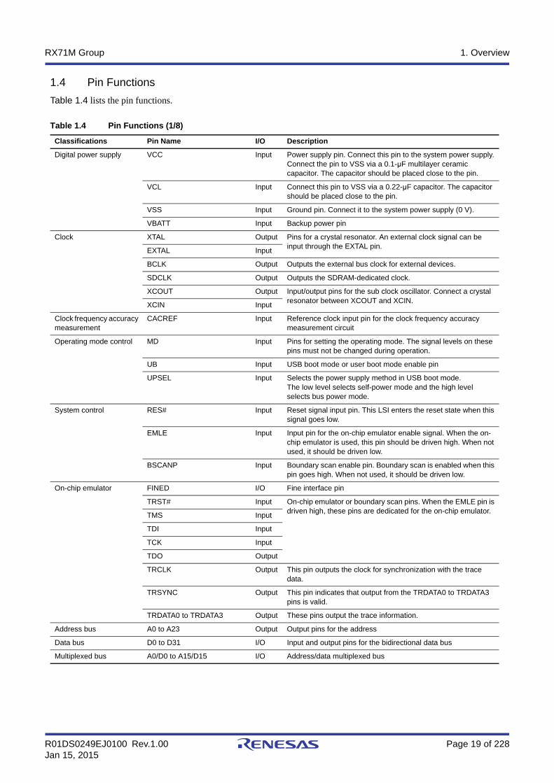
1.4 Pin Functions
Table 1.4 lists the pin functions.
Table 1.4 Pin Functions (1/8)
Classifications Pin Name I/O Description
Digital power supply VCC Input Power supply pin. Connect this pin to the system power supply. Connect the pin to VSS via a 0.1-μF multilayer ceramic capacitor. The capacitor should be placed close to the pin.
VCL Input Connect this pin to VSS via a 0.22-μF capacitor. The capacitor should be placed close to the pin.
VSS Input Ground pin. Connect it to the system power supply (0 V).
VBATT Input Backup power pin
Clock XTAL Output Pins for a crystal resonator. An external clock signal can be input through the EXTAL pin.
EXTAL Input
BCLK Output Outputs the external bus clock for external devices.
SDCLK Output Outputs the SDRAM-dedicated clock.
XCOUT Output Input/output pins for the sub clock oscillator. Connect a crystal resonator between XCOUT and XCIN.
XCIN Input
Clock frequency accuracy measurement
CACREF Input Reference clock input pin for the clock frequency accuracy measurement circuit
Operating mode control MD Input Pins for setting the operating mode. The signal levels on these pins must not be changed during operation.
UB Input USB boot mode or user boot mode enable pin
UPSEL Input Selects the power supply method in USB boot mode.The low level selects self-power mode and the high level selects bus power mode.
System control RES# Input Reset signal input pin. This LSI enters the reset state when this signal goes low.
EMLE Input Input pin for the on-chip emulator enable signal. When the on-chip emulator is used, this pin should be driven high. When not used, it should be driven low.
BSCANP Input Boundary scan enable pin. Boundary scan is enabled when this pin goes high. When not used, it should be driven low.
On-chip emulator FINED I/O Fine interface pin
TRST# Input On-chip emulator or boundary scan pins. When the EMLE pin is driven high, these pins are dedicated for the on-chip emulator.
TMS Input
TDI Input
TCK Input
TDO Output
TRCLK Output This pin outputs the clock for synchronization with the trace data.
TRSYNC Output This pin indicates that output from the TRDATA0 to TRDATA3 pins is valid.
TRDATA0 to TRDATA3 Output These pins output the trace information.
Address bus A0 to A23 Output Output pins for the address
Data bus D0 to D31 I/O Input and output pins for the bidirectional data bus
Multiplexed bus A0/D0 to A15/D15 I/O Address/data multiplexed bus

RX71M Group 1. Overview
R01DS0249EJ0100 Rev.1.00 Page 20 of 228Jan 15, 2015
Bus control RD# Output Strobe signal which indicates that reading from the external bus interface space is in progress
WR# Output Strobe signal which indicates that writing to the external bus interface space is in progress, in 1-write strobe mode
WR0# to WR3# Output Strobe signals which indicate that either group of data bus pins (D7 to D0, D15 to D8, D23 to D16 and D31 to D24) is valid in writing to the external bus interface space, in byte strobe mode
BC0# to BC3# Output Strobe signals which indicate that either group of data bus pins (D7 to D0, D15 to D8, D23 to D16 and D31 to D24) is valid in access to the external bus interface space, in 1-write strobe mode
ALE Output Address latch signal when address/data multiplexed bus is selected
WAIT# Input Input pin for wait request signals in access to the external space
CS0# to CS7# Output Select signals for CS areas
CKE Output SDRAM clock enable signal
SDCS# Output SDRAM chip select signal
RAS# Output SDRAM row address strobe signal
CAS# Output SDRAM column address strove signal
WE# Output SDRAM write enable pin
DQM0 to DQM3 Output SDRAM I/O data mask enable signals
EXDMA controller EDREQ0, EDREQ1 Input External DMA transfer request pins
EDACK0, EDACK1 Output Single address transfer acknowledge signals
Interrupt NMI Input Non-maskable interrupt request pin
IRQ0 to IRQ15 Input Maskable interrupt request pins
Multi-function timer pulse unit 3
MTIOC0A, MTIOC0BMTIOC0C, MTIOC0D
I/O The TGRA0 to TGRD0 input capture input/output compare output/PWM output pins
MTIOC1A, MTIOC1B I/O The TGRA1 and TGRB1 input capture input/output compare output/PWM output pins
MTIOC2A, MTIOC2B I/O The TGRA2 and TGRB2 input capture input/output compare output/PWM output pins
MTIOC3A, MTIOC3BMTIOC3C, MTIOC3D
I/O The TGRA3 to TGRD3 input capture input/output compare output/PWM output pins
MTIOC4A, MTIOC4BMTIOC4C, MTIOC4D
I/O The TGRA4 to TGRD4 input capture input/output compare output/PWM output pins
MTIC5U, MTIC5VMTIC5W
Input The TGRU5, TGRV5, and TGRW5 input capture input/dead time compensation input pins
MTIOC6A, MTIOC6BMTIOC6C, MTIOC6D
I/O The TGRA6 to TGRD6 input capture input/output compare output/PWM output pins
MTIOC7A, MTIOC7BMTIOC7C, MTIOC7D
I/O The TGRA7 to TGRD7 input capture input/output compare output/PWM output pins
MTIOC8A, MTIOC8BMTIOC8C, MTIOC8D
I/O The TGRA8 to TGRD8 input capture input/output compare output/PWM output pins
MTCLKA, MTCLKBMTCLKC, MTCLKD
Input Input pins for external clock signals or for phase counting mode clock signals
Port output enable 3 POE0#, POE4#, POE8#,POE10#, POE11#
Input Input pins for request signals to place the MTU or GPT in the high impedance state
Table 1.4 Pin Functions (2/8)
Classifications Pin Name I/O Description

RX71M Group 1. Overview
R01DS0249EJ0100 Rev.1.00 Page 21 of 228Jan 15, 2015
General-purpose PWM timer
GTIOC0A-A/GTIOC0A-B/GTIOC0A-C/GTIOC0A-D/GTIOC0A-E,GTIOC0B-A/GTIOC0B-B/GTIOC0B-C/GTIOC0B-D/GTIOC0B-E
I/O GPT0.GTGRA and GPT0.GTGRB input capture input/output compare output/PWM output pins
GTIOC1A-A/GTIOC1A-B/GTIOC1A-C/GTIOC1A-D/GTIOC1A-E,GTIOC1B-A/GTIOC1B-B/GTIOC1B-C/GTIOC1B-D/GTIOC1B-E
I/O GPT1.GTGRA and GPT1.GTGRB input capture input/output compare output/PWM output pins
GTIOC2A-A/GTIOC2A-B/GTIOC2A-C/GTIOC2A-D/GTIOC2A-E,GTIOC2B-A/GTIOC2B-B/GTIOC2B-C/GTIOC2B-D/GTIOC2B-E
I/O GPT2.GTGRA and GPT2.GTGRB input capture input/output compare output/PWM output pins
GTIOC3A-D/GTIOC3A-E, GTIOC3B-D/GTIOC3B-E
I/O GPT3.GTGRA and GPT3.GTGRB input capture input/output compare output/PWM output pins
GTETRG-B/GTETRG-C/GTETRG-D
Input External trigger input pin for GPT0 to GPT3
16-bit timer pulse unit TIOCA0, TIOCB0TIOCC0, TIOCD0
I/O The TGRA0 to TGRD0 input capture input/output compare output/PWM output pins
TIOCA1, TIOCB1 I/O The TGRA1 and TGRB1 input capture input/output compare output/PWM output pins
TIOCA2, TIOCB2 I/O The TGRA2 and TGRB2 input capture input/output compare output/PWM output pins
TIOCA3, TIOCB3TIOCC3, TIOCD3
I/O The TGRA3 to TGRD3 input capture input/output compare output/PWM output pins
TIOCA4, TIOCB4 I/O The TGRA4 and TGRB4 input capture input/output compare output/PWM output pins
TIOCA5, TIOCB5 I/O The TGRA5 and TGRB5 input capture input/output compare output/PWM output pins
TCLKA, TCLKBTCLKC, TCLKD
Input Input pins for external clock signals or for phase counting mode clock signals
Programmable pulse generator
PO0 to PO31 Output Output pins for the pulse signals
8-bit timer TMO0 to TMO3 Output Compare match output pins
TMCI0 to TMCI3 Input Input pins for external clocks to be input to the counter
TMRI0 to TMRI3 Input Input pins for the counter reset
Compare match timer W TIC0 to TIC3 Input Input pins for CMTW
TOC0 to TOC3 Output Output pins for CMTW
Table 1.4 Pin Functions (3/8)
Classifications Pin Name I/O Description

RX71M Group 1. Overview
R01DS0249EJ0100 Rev.1.00 Page 22 of 228Jan 15, 2015
Serial communications interface (SCIg)
Asynchronous mode/clock synchronous mode
SCK0 to SCK7 I/O Input/output pins for the clock
RXD0 to RXD7 Input Input pins for received data
TXD0 to TXD7 Output Output pins for transmitted data
CTS0# to CTS7# Input Input pins for controlling the start of transmission and reception
RTS0# to RTS7# Output Output pins for controlling the start of transmission and reception
Simple I2C mode
SSCL0 to SSCL7 I/O Input/output pins for the I2C clock
SSDA0 to SSDA7 I/O Input/output pins for the I2C data
Simple SPI mode
SCK0 to SCK7 I/O Input/output pins for the clock
SMISO0 to SMISO7 I/O Input/output pins for slave transmission of data
SMOSI0 to SMOSI7 I/O Input/output pins for master transmission of data
SS0# to SS7# Input Chip-select input pins
Serial communications interface (SCIh)
Asynchronous mode/clock synchronous mode
SCK12 I/O Input/output pin for the clock
RXD12 Input Input pin for received data
TXD12 Output Output pin for transmitted data
CTS12# Input Input pin for controlling the start of transmission and reception
RTS12# Output Output pin for controlling the start of transmission and reception
Simple I2C mode
SSCL12 I/O Input/output pin for the I2C clock
SSDA12 I/O Input/output pin for the I2C data
Simple SPI mode
SCK12 I/O Input/output pin for the clock
SMISO12 I/O Input/output pin for slave transmission of data
SMOSI12 I/O Input/output pin for master transmission of data
SS12# Input Chip-select input pin
Extended serial mode
RXDX12 Input Input pin for received data
TXDX12 Output Output pin for transmitted data
SIOX12 I/O Input/output pin for received or transmitted data
Serial communications interface with FIFO(SCIFA)
SCK8 to SCK11 I/O Input/output pins for the clock
RXD8 to RXD11 Input Input pins for received data
TXD8 to TXD11 Output Output pins for transmitted data
CTS8# to CTS11# Input Input pins for controlling the start of transmission and reception
RTS8# to RTS11# Output Output pins for controlling the start of transmission and reception
I2C bus interface SCL0[FM+], SCL2 I/O Input/output pins for clocks. Bus can be directly driven by the N-channel open drain
SDA0[FM+], SDA2 I/O Input/output pins for data. Bus can be directly driven by the N-channel open drain
Table 1.4 Pin Functions (4/8)
Classifications Pin Name I/O Description

RX71M Group 1. Overview
R01DS0249EJ0100 Rev.1.00 Page 23 of 228Jan 15, 2015
Ethernet controller REF50CK0, REF50CK1 Input 50-MHz reference clocks. These pins input reference signals for transmission/reception timings in RMII mode.
RMII0_CRS_DV,RMII1_CRS_DV
Input Indicate that there are carrier detection signals and valid receive data on RMII_RXD1 and RMII_RXD0 in RMII mode.
RMII0_TXD0, RMII0_TXD1,RMII1_TXD0, RMII1_TXD1
Output 2-bit transmit data in RMII mode
RMII0_RXD0, RMII0_RXD1,RMII1_RXD0, RMII1_RXD1
Input 2-bit receive data in RMII mode
RMII0_TXD_EN,RMII1_TXD_EN
Output Output pins for data transmit enable signals in RMII mode
RMII0_RX_ER, RMII1_RX_ER
Input Indicate an error has occurred during reception of data in RMII mode.
ET0_CRS,ET1_CRS
Input Carrier detection/data reception enable pins
ET0_RX_DV,ET1_RX_DV
Input Indicate that there are valid receive data on ET_ERXD3 to ET_ERXD0.
ET0_EXOUT,ET1_EXOUT
Output General-purpose external output pins
ET0_LINKSTAET1_LINKSTA
Input Input link status from the PHY-LSI.
ET0_ETXD0 to ET0_ETXD3, ET1_ETXD0 to ET1_ETXD3
Output 4 bits of MII transmit data
ET0_ERXD0 to ET0_ERXD3,ET1_ERXD0 to ET1_ERXD3
Input 4 bits of MII receive data
ET0_TX_EN,ET1_TX_EN
Output Transmit enable pins. Function as signals indicating that transmit data is ready on ET_ETXD3 to ET_ETXD0.
ET0_TX_ER,ET1_TX_ER
Output Transmit error pins. Function as signals notifying the PHY-LSI of an error during transmission.
ET0_RX_ER,ET1_RX_ER
Input Receive error pins. Function as signals to recognize an error during reception.
ET0_TX_CLK,ET1_TX_CLK
Input Transmit clock pins. These pins input reference signals for output timings from ET_TX_EN, ET_ETXD3 to ET_ETXD0, and ET_TX_ER.
ET0_RX_CLK,ET1_RX_CLK
Input Receive clock pins. These pins input reference signals for input timings to ET_RX_DV, ET_ERXD3 to ET_ERXD0, and ET_RX_ER.
ET0_COL, ET1_COL Input Input collision detection signals.
ET0_WOL, ET1_WOL Output Receive Magic packets.
ET0_MDC, ET1_MDC Output Output reference clock signals for information transfer via ET_MDIO.
ET0_MDIO, ET1_MDIO I/O Input or output bidirectional signals for exchange of management information between this MCU and the PHY-LSI.
Table 1.4 Pin Functions (5/8)
Classifications Pin Name I/O Description

RX71M Group 1. Overview
R01DS0249EJ0100 Rev.1.00 Page 24 of 228Jan 15, 2015
USB 2.0 host/function module
VCC_USB,VCC_USBA
Input Power supply pins
VSS_USB,VSS1_USBA,VSS2_USBA
Input Ground pins
AVCC_USBA Input USBA analog power supply pin
AVSS_USBA Input USBA analog ground pin. Short this pin with the PVSS_USBA pin.
PVSS_USBA Input USBA PLL circuit ground pin. Short this pin with the AVSS_USBA pin.
USBA_RREF I/O USBA reference current supply pin. Connect 2.2 KΩ (1%) to the AVSS_USBA pin.
USB0_DP,USBA_DP
I/O Input or output USB transceiver D+ data.
USB0_DM,USBA_DM
I/O Input or output USB transceiver D- data.
USB0_EXICEN,USBA_EXICEN
Output Connect to the OTG power IC.
USB0_ID, USBA_ID Input Connect to the OTG power IC.
USB0_VBUSENUSBA_VBUSEN
Output USB VBUS power enable pins
USB0_OVRCURA/USB0_OVRCURB,USBA_OVRCURA/USBA_OVRCURB
Input USB overcurrent pins
USB0_VBUS, USBA_VBUS
Input USB cable connection/disconnection detection input pins
CAN module CRX0, CRX1-DS, CRX2 Input Input pins
CTX0 to CTX2 Output Output pins
Serial peripheral interface RSPCKA-A/RSPCKA-B/RSPCKB-A/RSPCKB-B
I/O Clock input/output pin
MOSIA-A/MOSIA-B/MOSIB-A/MOSIB-B
I/O Inputs or outputs data output from the master
MISOA-A/MISOA-B/MISOB-A/MISOB-B
I/O Inputs or outputs data output from the slave
SSLA0-A/SSLA0-B/SSLB0-A/SSLB0-B
I/O Input or output pin for slave selection
SSLA1-A/SSLA1-B/SSLB1-A/SSLB1-B to SSLA3-A/SSLA3-B/SSLB3-A/SSLB3-B
Output Output pin for slave selection
Quad serial peripheral interface
QSPCLK-A/-B Output QSPI clock output pin
QSSL-A/-B Output QSPI slave output pin
QMO-A/-B, QIO0-A/-B I/O Master transmit data/data 0
QMI-A/-B, QIO1-A/-B I/O Master input data/data 1
QIO2-A/-B, QIO3-A/-B I/O Data 2, data 3
Serial sound interface SSISCK0, SSISCK1 I/O SSI serial bit clock pins
SSIWS0, SSIWS1 I/O Word select pins
SSITXD0, SSITXD1 Output Serial data output pins
SSIRXD0, SSIRXD1 Input Serial data input pins
SSIDATA0, SSIDATA1 I/O Serial data input/output pins
AUDIO_MCLK Input Master clock pin for audio
Table 1.4 Pin Functions (6/8)
Classifications Pin Name I/O Description

RX71M Group 1. Overview
R01DS0249EJ0100 Rev.1.00 Page 25 of 228Jan 15, 2015
MMC host interface MMC_CLK-A/MMC_CLK-B
Output MMC clock pin
MMC_CMD-A/MMC_CMD-B
I/O Command/response pin
MMC_D7-A/MMC_D7-B to MMC_D0-A/MMC_D0-B
I/O Transmit data/receive data
MMC_CD-A/MMC_CD-B Input Card detection pin
MMC_RES#-A/MMC_RES#-B Output MMC reset output pin
SD host interface SDHI_CLK-A/SDHI_CLK-B Output SD clock output pin
SDHI_CMD-A/SDHI_CMD-B I/O SD command output, response input signal pin
SDHI_D3-A/SDHI_D3-B to SDHI_D0-A/SDHI_D0-B
I/O SD data bus pins
SDHI_CD-A/SDHI_CD-B Input SD card detection pin
SDHI_WP-A/SDHI_WP-B Input SD write-protect signal
Parallel data capture unit PIXCLK Input Image transfer clock pin
VSYNC Input Vertical synchronization signal pin
HSYNC Input Horizontal synchronization signal pin
PIXD0 to PIXD7 Input 8-bit image data pins
PCKO Output Output pin for dot clock
Realtime clock RTCOUT Output Output pin for 1-Hz/64-Hz clock
RTCIC0 to RTCIC2 Input Time capture event input pins
12-bit A/D converter AN000 to AN007, AN100 to AN120
Input Input pins for the analog signals to be processed by the A/D converter
ADTRG0#, ADTRG1# Input Input pins for the external trigger signals that start the A/D conversion
ANEX0 Output Extended analog output pin
ANEX1 Input Extended analog input pin
12-bit D/A converter DA0, DA1 Output Output pins for the analog signals to be processed by the D/A converter
Analog power supply AVCC0 Input Analog voltage supply pin for the 12-bit A/D converter (unit 0). Connect this pin to a branch from the VCC power supply.
AVSS0 Input Analog ground pin for the 12-bit A/D converter (unit 0). Connect this pin to a branch from the VSS ground power supply.
VREFH0 Input Analog reference voltage supply pin for the 12-bit A/D converter (unit 0). Connect this pin to VCC if the 12-bit A/D converter is not to be used.
VREFL0 Input Analog reference ground pin for the 12-bit A/D converter (unit 0). Connect this pin to VSS if the 12-bit A/D converter is not to be used.
AVCC1 Input Analog voltage supply and reference voltage supply pin for the 12-bit A/D converter (unit 1) and D/A converter. This pin also supplies the analog voltage to the temperature sensor. Connect this pin to a branch from the VCC power supply.
AVSS1 Input Analog voltage supply and reference voltage supply pin for the 12-bit A/D converter (unit 1) and D/A converter. This pin also supplies the analog ground voltage to the temperature sensor. Connect this pin to a branch from the VSS ground power supply.
Table 1.4 Pin Functions (7/8)
Classifications Pin Name I/O Description

RX71M Group 1. Overview
R01DS0249EJ0100 Rev.1.00 Page 26 of 228Jan 15, 2015
Note: Note the following regarding pin names. For details, see section 1.5, Pin Assignments. We recommend using pins that have a letter (“-A”, “-B”, etc.) to indicate group membership appended to their names as groups.
For the RSPI, QSPI, SDHI, and MMC interfaces, the AC portion of the electrical characteristics is measured for each group. Pins that have "-DS" appended to their names can be used as triggers for release from deep software standby. RIIC pin functions that have [FM+] appended to their names support fast-mode plus.
I/O ports P00 to P03, P05, P07 I/O 6-bit input/output pins
P10 to P17 I/O 8-bit input/output pins
P20 to P27 I/O 8-bit input/output pins
P30 to P37 I/O 8-bit input/output pins (P35: input pin)
P40 to P47 I/O 8-bit input/output pins
P50 to P56 I/O 7-bit input/output pins(176-pin devices have only P50 to P53)
P60 to P67 I/O 8-bit input/output pins
P70 to P77 I/O 8-bit input/output pins
P80 to P83, P86, P87 I/O 6-bit input/output pins
P90 to P97 I/O 8-bit input/output pins
PA0 to PA7 I/O 8-bit input/output pins
PB0 to PB7 I/O 8-bit input/output pins
PC0 to PC7 I/O 8-bit input/output pins
PD0 to PD7 I/O 8-bit input/output pins
PE0 to PE7 I/O 8-bit input/output pins
PF0 to PF5 I/O 6-bit input/output pins
PG0 to PG7 I/O 8-bit input/output pins
PJ3, PJ5 I/O 2-bit input/output pins
Table 1.4 Pin Functions (8/8)
Classifications Pin Name I/O Description

RX71M Group 1. Overview
R01DS0249EJ0100 Rev.1.00 Page 27 of 228Jan 15, 2015
1.5 Pin Assignments
Figure 1.3 to Figure 1.9 show the pin assignments. Table 1.5 to Table 1.10 show the lists of pins and pin functions.
Figure 1.3 Pin Assignment (177-Pin TFLGA)
A B C D E F G H J K L M N P R
15 PE2 PE3 P70 P65 P67 VSS VCC PG7 PA6 PB0 P72 PB4 VSS VCC PC1 15
14 PE1 PE0 VSS PE7 PG3 PA0 PA1 PA2 PA7 VCC PB1 PB5 P73 P75 P74 14
13 P63 P64 PE4 VCC PG2 PG4 PG6 PA3 VSS P71 PB3 PB7 PC0 PC2 P76 13
12 P60 VSS P62 PE5 PE6 P66 PG5 PA4 PA5 PB2 PB6 P77 PC3 PC4 P80 12
11 PD6 PG1 VCC P61
RX71M GroupPTLG0177KA-A(177-Pin TFLGA)
(Upper Perspective View)
P81 P82 PC6 VCC 11
10 P97 PD4 PG0 PD7 PC5 PC7 P83 VSS 10
9 VCC P96 PD3 PD5 P50 P51 P52 P53 9
8 P94 PD1 PD2 VSSVCC_USBA
VSS1_USBA
P10 P11 8
7 VSS P92 PD0 P95USBA_RREF
VSS2_USBA
USBA_DM
USBA_DP
7
6 VCC P91 P90 P93AVCC_USBA
VSS_USB
AVSS_USBA
PVSS_USBA
6
5 P46 P47 P45 P44 NCVCC_USB
P12USB0_
DPUSB0_
DM5
4 P42 P41 P43 P00 VSS BSCANP PF4 P35 PF3 PF1 P25 P86 P15 P14 P13 4
3 VREFL0 P40 VREFH0 P03 PF5 PJ3MD/
FINEDRES# P34 PF2 PF0 P24 P22 P87 P16 3
2 AVCC0 P07 AVCC1 P02 EMLE VCL XCOUT VSS VCC P32 P30 P26 P23 P17 P20 2
1 AVSS0 P05 AVSS1 P01 PJ5 VBATT XCIN XTAL EXTAL P33 P31 P27 VCC VSS P21 1
A B C D E F G H J K L M N P R
Note: This figure indicates the power supply pins and I/O port pins. For the pin configuration, see Table 1.5, List of Pin and Pin Functions (177-Pin TFLGA, 176-Pin LFBGA).

RX71M Group 1. Overview
R01DS0249EJ0100 Rev.1.00 Page 28 of 228Jan 15, 2015
Figure 1.4 Pin Assignment (176-Pin LFBGA)
A B C D E F G H J K L M N P R
15 PE2 PE3 P70 P65 P67 VSS VCC PG7 PA6 PB0 P72 PB4 VSS VCC PC1 15
14 PE1 PE0 VSS PE7 PG3 PA0 PA1 PA2 PA7 VCC PB1 PB5 P73 P75 P74 14
13 P63 P64 PE4 VCC PG2 PG4 PG6 PA3 VSS P71 PB3 PB7 PC0 PC2 P76 13
12 P60 VSS P62 PE5 PE6 P66 PG5 PA4 PA5 PB2 PB6 P77 PC3 PC4 P80 12
11 PD6 PG1 VCC P61
RX71M GroupPLBG0176GA-A(176-Pin LFBGA)
(Upper Perspective View)
P81 P82 PC6 VCC 11
10 P97 PD4 PG0 PD7 PC5 PC7 P83 VSS 10
9 VCC P96 PD3 PD5 P50 P51 P52 P53 9
8 P94 PD1 PD2 VSSVCC_USBA
VSS1_USBA
P10 P11 8
7 VSS P92 PD0 P95USBA_RREF
VSS2_USBA
USBA_DM
USBA_DP
7
6 VCC P91 P90 P93AVCC_USBA
VSS_USB
AVSS_USBA
PVSS_USBA
6
5 P46 P47 P45 P44VCC_USB
P12USB0_
DPUSB0_
DM5
4 P42 P41 P43 P00 VSS BSCANP PF4 P35 PF3 PF1 P25 P86 P15 P14 P13 4
3 VREFL0 P40 VREFH0 P03 PF5 PJ3MD/
FINEDRES# P34 PF2 PF0 P24 P22 P87 P16 3
2 AVCC0 P07 AVCC1 P02 EMLE VCL XCOUT VSS VCC P32 P30 P26 P23 P17 P20 2
1 AVSS0 P05 AVSS1 P01 PJ5 VBATT XCIN XTAL EXTAL P33 P31 P27 VCC VSS P21 1
A B C D E F G H J K L M N P R
Note: This figure indicates the power supply pins and I/O port pins. For the pin configuration, see Table 1.5, List of Pin and Pin Functions (177-Pin TFLGA, 176-Pin LFBGA).

RX71M Group 1. Overview
R01DS0249EJ0100 Rev.1.00 Page 29 of 228Jan 15, 2015
Figure 1.5 Pin Assignment (176-Pin LQFP)
1 2 3 4 5 6 7 8 9 10 11 12 13 14 15 16 17 18 19 20 21 22 23 24 25 26 27 28 29 30 31 32 33 34 35 36 37 38 39 40 41 42 43 44
132
131
130
129
128
127
126
125
124
123
122
121
120
119
118
117
116
115
114
113
112
111
110
109
108
107
106
105
104
103
102
101
100 99 98 97 96 95 94 93 92 91 90 89
88
87
86
85
84
83
82
81
80
79
78
77
76
75
74
73
72
71
70
69
68
67
66
65
64
63
62
61
60
59
58
57
56
55
54
53
52
51
50
49
48
47
46
45
133
134
135
136
137
138
139
140
141
142
143
144
145
146
147
148
149
150
151
152
153
154
155
156
157
158
159
160
161
162
163
164
165
166
167
168
169
170
171
172
173
174
175
176
PE0P64P63P62P61VSSP60
VCCPD7PG1PD6PG0
PD4P97PD3VSSP96
VCCPD2P95PD1P94PD0P93
P91
P90
P47
P45
P43
P41
P40
P07
PE1
PD5
AVCC0P20
PE
3
PE
5V
SS
P70
VC
CP
E6
PE
7P
65P
G2
P66
PG
3P
67P
G4
VS
SP
G5
VC
CP
A1
PG
6P
A2
PG
7P
A3
PA
4P
A5
PA
6P
A7
PB
0V
CC
PB
1P
B2
PB
4
PB
6
P73
PC
1
PE
4
PA
0
VC
C
AV
SS
0
AV
CC
1P
03
AV
SS
1P
02
P0
1P
00
PF
5E
ML
EP
J5V
SS
PJ3
VC
L
NC
PF
4M
D/F
INE
DX
CIN
XC
OU
TR
ES
#P
37/
XT
AL
VS
S
VC
C
P3
4
PF
2
P3
0
PF
0
P2
6
VC
C
VS
SP
23
P2
1
P36
/EX
TA
L
P0
5
VB
AT
T
P3
2
PE2
P3
5
P3
3
PF
3
P3
1
PF
1
P2
7
P2
5
P2
4
P2
2
P17P87P16P86P15P14P13P12VCC_USBUSB0_DMUSB0_DPVSS_USBAVCC_USBAUSBA_RREFAVSS_USBAPVSS_USBAVSS2_USBA
USBA_DPVSS1_USBA
P83
PC7PC6PC5P82P81P80PC4PC3P77
USBA_DM
VCC_USBAP11P10P53P52P51P50VSS
VCC
P76PC2P75P74
VS
S
P71
P72
PB
3
PB
5
PB
7
PC
0V
SS
P92
VSS
VCC
P46
P44
P42
VREFH0
VREFL0
Note: This figure indicates the power supply pins and I/O port pins. For the pin configuration, see Table 1.6, List of Pin and Pin Functions (176-Pin LQFP).
RX71M GroupPLQP0176KB-A(176-pin LQFP)
(Top view)

RX71M Group 1. Overview
R01DS0249EJ0100 Rev.1.00 Page 30 of 228Jan 15, 2015
Figure 1.6 Pin Assignment (145-Pin TFLGA)
A B C D E F G H J K L M N
13 PE3 PE4 VSS PE6 P67 PA2 PA4 PA7 PB1 PB5 VSS VCC P74 13
12 PE1 PE2 P70 PE5 P65 PA1 VCC PB0 PB2 PB6 P73 PC1 P75 12
11 P62 P61 PE0 VCC P66 VSS PA6 P71 PB4 PB7 PC2 PC0 PC3 11
10 VSS VCC P63 PE7 PA0 PA3 PA5 P72 PB3 P76 PC4 P77 P82 10
9 PD6 PD4 PD7 P64
RX71M GroupPTLG0145KA-A(145-Pin TFLGA)(Upper Perspective
View)
P80 PC5 P81 PC7 9
8 PD2 PD0 PD3 P60 VCC P83 PC6 VSS 8
7 P92 P91 PD1 PD5 P51 P52 P50 P55 7
6 P90 P47 VSS P93 P53 P56VSS_USB
USB0_DP
6
5 P45 P43 P46 VCC P44 P54 P13VCC_USB
USB0_DM
5
4 P42 VREFL0 P41 P01 EMLE VBATT BSCANP P35 P30 P15 P24 P12 P14 4
3 P40 P05 VREFH0 P03 PJ5 PJ3MD/
FINEDVSS P32 P31 P16 P86 P87 3
2 P07 AVCC0 P02 PF5 VCL XCOUT RES# VCC P33 P26 P23 P17 P20 2
1 AVSS0 AVCC1 AVSS1 P00 VSS XCIN XTAL EXTAL P34 P27 P25 P22 P21 1
A B C D E F G H J K L M N
Note: This figure indicates the power supply pins and I/O port pins. For the pin configuration, see Table 1.7, List of Pin and Pin Functions (145-Pin TFLGA).

RX71M Group 1. Overview
R01DS0249EJ0100 Rev.1.00 Page 31 of 228Jan 15, 2015
Figure 1.7 Pin Assignment (144-Pin LQFP)
1 2 3 4 5 6 7 8 9 10 11 12 13 14 15 16 17 18 19 20 21 22 23 24 25 26 27 28 29 30 31 32 33 34 35 36
108
107
106
105
104
103
102
101
100 99 98 97 96 95 94 93 92 91 90 89 88 87 86 85 84 83 82 81 80 79 78 77 76 75 74 73
72
71
70
69
68
67
66
65
64
63
62
61
60
59
58
57
56
55
54
53
52
51
50
49
48
47
46
45
44
43
42
41
40
39
38
37
109
110
111
112
113
114
115
116
117
118
119
120
121
122
123
124
125
126
127
128
129
130
131
132
133
134
135
136
137
138
139
140
141
142
143
144
PE0
P64
P63
P62
P61
VSS
P60
VCC
PD7
PD6
PD5
PD4
PD2
PD1PD0
P93
P92
P91
VSS
P90VCC
P47
P46
P45
P44
P43
P42
P41
VREFL0
P40
VREFH0
P07
PE1
PD3
AVCC0
P74
PC2
P76
P77
PC3
PC4
P80
P81
P82
PC5
PC6
PC7
VCC
VSS
P50
P51
P52
P53
P54
P55
P56
VSS_USB
USB0_DPUSB0_DM
VCC_USB
P12
P13
P14
P15
P86
P16
P87
P20
P75
P83
P17
PE
3
PE
5
VS
S
P70
VC
C
PE
6
PE
7
P65
P66
P67
PA
0
PA
1
PA
2
VS
S
PA
4
VC
C
PA
5
PA
6
PA
7
PB
0
P71
P72
PB
1
PB
2
PB
3
PB
4
PB
5
PB
6
PB
7
P73
VS
S
PC
0
PC
1
PE
4
PA
3
VC
C
AV
SS
0
AV
CC
1
P0
3
AV
SS
1
P0
2
P0
1
P0
0
PF
5
EM
LE
PJ5
VS
S
PJ3
VC
L
MD
/FIN
ED
XC
IN
XC
OU
TR
ES
#
P3
7/X
TA
L
VS
S
P3
6/E
XT
AL
VC
C
P3
5
P3
4
P3
2
P3
1
P3
0
P2
7
P2
6
P25
P24
P2
3
P2
1
P0
5
VB
AT
T
P2
2
P3
3
PE2
Note: This figure indicates the power supply pins and I/O port pins. For the pin configuration, see Table 1.8, List of Pin and Pin Functions (144-Pin LQFP).
RX71M GroupPLQP0144KA-A(144-pin LQFP)
(Top view)

RX71M Group 1. Overview
R01DS0249EJ0100 Rev.1.00 Page 32 of 228Jan 15, 2015
Figure 1.8 Pin Assignment (100-Pin TFLGA)
RX71M Group
PTLG0100JA-A (100-Pin TFLGA)
(Upper Perspective View)
A B C D E F G H J K
10 PE2 PE3 PE4 PA0 PA3 VSS VCC PB7 PC1 PC2 10
9 PE1 PD7 PE5 PA1 PA5 PA7 PB1 PB6 PC0 PC3 9
8 PE0 PD6 PD5 PE7 PA4 PB0 PB4 PC6 PC4 PC5 8
7 PD4 PD3 PD2 PE6 PA6 PB2 PB5 PC7 P50 P51 7
6 PD0 PD1 P47 P46 PA2 PB3 P52 P54VCC_
USB
USB0_
DP6
5 P43 P44 P42 P45 P41 P12 P53 P55VSS_
USB
USB0_
DM5
4 VREFL0 P40 VREFH0 VBATT P34 P32 P27 P15 P13 P14 4
3 P07 AVCC0 PJ3MD/
FINEDRES# P35 P30 P16 P17 P20 3
2 AVCC1 AVSS0 AVSS1 XCOUT VSS VCC P31 P25 P21 P22 2
1 P05 EMLE VCL XCIN XTAL EXTAL P33 P26 P24 P23 1
A B C D E F G H J K
Note: This figure indicates the power supply pins and I/O port pins. For the pin configuration, see Table 1.9, List of Pin and Pin Functions (100-Pin TFLGA).

RX71M Group 1. Overview
R01DS0249EJ0100 Rev.1.00 Page 33 of 228Jan 15, 2015
Figure 1.9 Pin Assignment (100-Pin LQFP)
1 2 3 4 5 6 7 8 9 10 11 12 13 14 15 16 17 18 19 20 21 22 23 24 25
75 74 73 72 71 70 69 68 67 66 65 64 63 62 61 60 59 58 57 56 55 54 53 52 51
50
49
48
47
46
45
44
43
42
41
40
39
38
37
36
35
34
33
32
31
30
29
28
27
26
76
77
78
79
80
81
82
83
84
85
86
87
88
89
90
91
92
93
94
95
96
97
98
99
100
PE0
PD7
PD6
PD5
PD4
PD3
PD2
PD1
PD0
P47
P46
P45
P43
P42
P41
VREFL0
P40
VREFH0
AVCC0
P07
AVSS0
PE1
P44
PC2
PC4
PC5
PC6
PC7
P50
P51
P52
P53
P54
P55
VSS_USB
USB0_DP
VCC_USB
P12
P13
P14
P15
P16
P17
P20
P21
P22
PC3
USB0_DM
PE
3
PE
5
PE
6
PE
7
PA
0
PA
1
PA
2
PA
3
PA
4
PA
5
PA
6
PA
7
VS
S
VC
C
PB
1
PB
2
PB
3
PB
4
PB
5
PB
6
PB
7
PC
0
PC
1
PE
4
PB
0
AV
CC
1
AV
SS
1
PJ3
VC
L
VB
AT
T
MD
/FIN
ED
XC
IN
XC
OU
T
RE
S#
P37
/XT
AL
VS
S
P36
/EX
TA
L
P35
P34
P33
P32
P31
P30
P27
P26
P25
P23
EM
LE
VC
C
PE2
P05
P24
Note: This figure indicates the power supply pins and I/O port pins. For the pin configuration, see Table 1.10, List of Pin and Pin Functions (100-Pin LQFP).
RX71M GroupPLQP0100KB-A(100-pin LQFP)
(Top view)

RX71M Group 1. Overview
R01DS0249EJ0100 Rev.1.00 Page 34 of 228Jan 15, 2015
Table 1.5 List of Pin and Pin Functions (177-Pin TFLGA, 176-Pin LFBGA) (1/7)
Pin Number
Power SupplyClock System Control I/O Port
BusEXDMACSDRAMC
Timer CommunicationMemory InterfaceCamera Interface
InterruptS12ADC,R12DA
177-Pin TFLGA176-Pin LFBGA
(MTU, GPT, TPU, TMR, PPG, RTC, CMTW, POE, CAC)
(ETHERC, SCIg, SCIh, RSPI, RIIC, CAN, USB, SSI)
(QSPI, SDHI, MMCIF, PDC)
A1 AVSS0
A2 AVCC0
A3 VREFL0
A4 P42 IRQ10-DS
AN002
A5 P46 IRQ14-DS
AN006
A6 VCC
A7 VSS
A8 P94 A20/D20 ET1_ERXD0/RMII1_RXD0
A9 VCC
A10 P97 A23/D23 ET1_ERXD3
A11 PD6 D6[A6/D6] MTIC5V/MTIOC8A/POE4#
MMC_D0-B/SDHI_D0-B/QIO0-B/QMO-B
IRQ6 AN106
A12 P60 CS0# ET1_TX_EN/RMII1_TXD_EN
A13 P63 CS3#/CAS#
A14 PE1 D9[A9/D9] MTIOC4C/MTIOC3B/GTIOC1B-A/PO18
TXD12/SMOSI12/SSDA12/TXDX12/SIOX12/SSLB2-B
MMC_D5-B ANEX1
A15 PE2 D10[A10/D10] MTIOC4A/GTIOC0B-A/PO23/TIC3
RXD12/SMISO12/SSCL12/RXDX12/SSLB3-B
MMC_D6-B IRQ7-DS AN100
B1 P05 IRQ13 DA1
B2 P07 IRQ15 ADTRG0#
B3 P40 IRQ8-DS AN000
B4 P41 IRQ9-DS AN001
B5 P47 IRQ15-DS
AN007
B6 P91 A17/D17 ET1_COL/SCK7 AN115
B7 P92 A18/D18 POE4# ET1_CRS/RMII1_CRS_DV/RXD7/SMISO7/SSCL7
AN116
B8 PD1 D1[A1/D1] MTIOC4B/GTIOC1A-E/POE0#
CTX0 IRQ1 AN109
B9 P96 A22/D22 ET1_ERXD2
B10 PD4 D4[A4/D4] MTIOC8B/POE11# MMC_CMD-B/SDHI_CMD-B/QSSL-B
IRQ4 AN112
B11 PG1 D25 ET1_RX_ER/RMII1_RX_ER
B12 VSS
B13 P64 CS4#/WE#
B14 PE0 D8[A8/D8] MTIOC3D/GTIOC2B-A
SCK12/SSLB1-B MMC_D4-B ANEX0
B15 PE3 D11[A11/D11] MTIOC4B/GTIOC2A-A/PO26/POE8#/TOC3
CTS12#/RTS12#/SS12#/ET0_ERXD3
MMC_D7-B AN101
C1 AVSS1
C2 AVCC1
C3 VREFH0

RX71M Group 1. Overview
R01DS0249EJ0100 Rev.1.00 Page 35 of 228Jan 15, 2015
C4 P43 IRQ11-DS AN003
C5 P45 IRQ13-DS
AN005
C6 P90 A16/D16 ET1_RX_DV/TXD7/SMOSI7/SSDA7
AN114
C7 PD0 D0[A0/D0] GTIOC1B-E/POE4# IRQ0 AN108
C8 PD2 D2[A2/D2] MTIOC4D/GTIOC0B-E/TIC2
CRX0 MMC_D2-B/SDHI_D2-B/QIO2_B
IRQ2 AN110
C9 PD3 D3[A3/D3] MTIOC8D/GTIOC0A-E/POE8#/TOC2
MMC_D3-B/SDHI_D3-B/QIO3-B
IRQ3 AN111
C10 PG0 D24 ET1_RX_CLK/REF50CK1
C11 VCC
C12 P62 CS2#/RAS#
C13 PE4 D12[A12/D12] MTIOC4D/MTIOC1A/GTIOC1A-A/PO28
ET0_ERXD2/SSLB0-B AN102
C14 VSS
C15 P70 SDCLK
D1 P01 TMCI0 RXD6/SMISO6/SSCL6
IRQ9 AN119
D2 P02 TMCI1 SCK6 IRQ10 AN120
D3 P03 IRQ11 DA0
D4 P00 TMRI0 TXD6/SMOSI6/SSDA6
IRQ8 AN118
D5 P44 IRQ12-DS
AN004
D6 P93 A19/D19 POE0# ET1_LINKSTA/CTS7#/RTS7#/SS7#
AN117
D7 P95 A21/D21 ET1_ERXD1/RMII1_RXD1
D8 VSS
D9 PD5 D5[A5/D5] MTIC5W/MTIOC8C/POE10#
MMC_CLK-B/SDHI_CLK-B/QSPCLK-B
IRQ5 AN113
D10 PD7 D7[A7/D7] MTIC5U/POE0# MMC_D1-B/SDHI_D1-B/QIO1-B/QMI-B
IRQ7 AN107
D11 P61 CS1#/SDCS#
D12 PE5 D13[A13/D13] MTIOC4C/MTIOC2B/GTIOC0A-A
ET0_RX_CLK/REF50CK0/RSPCKB-B
IRQ5 AN103
D13 VCC
D14 PE7 D15[A15/D15] MTIOC6A/GTIOC3A-E/TOC1
MISOB-B MMC_RES#-B/SDHI_WP-B
IRQ7 AN105
D15 P65 CS5#/CKE
E1 PJ5 POE8# CTS2#/RTS2#/SS2#
E2 EMLE
E3 PF5 IRQ4
E4 VSS
E5*1
E12 PE6 D14[A14/D14] MTIOC6C/GTIOC3B-E/TIC1
MOSIB-B MMC_CD-B/SDHI_CD-B
IRQ6 AN104
Table 1.5 List of Pin and Pin Functions (177-Pin TFLGA, 176-Pin LFBGA) (2/7)
Pin Number
Power SupplyClock System Control I/O Port
BusEXDMACSDRAMC
Timer CommunicationMemory InterfaceCamera Interface
InterruptS12ADC,R12DA
177-Pin TFLGA176-Pin LFBGA
(MTU, GPT, TPU, TMR, PPG, RTC, CMTW, POE, CAC)
(ETHERC, SCIg, SCIh, RSPI, RIIC, CAN, USB, SSI)
(QSPI, SDHI, MMCIF, PDC)

RX71M Group 1. Overview
R01DS0249EJ0100 Rev.1.00 Page 36 of 228Jan 15, 2015
E13 TRDATA0 PG2 D26 ET1_TX_CLK
E14 TRDATA1 PG3 D27 ET1_ETXD0/RMII1_TXD0
E15 P67 CS7#/DQM1 MTIOC7C/GTIOC1B-C
CRX2 IRQ15
F1 VBATT
F2 VCL
F3 PJ3 EDACK1 MTIOC3C ET0_EXOUT/CTS6#/RTS6#/CTS0#/RTS0#/SS6#/SS0#
F4 BSCANP
F12 P66 CS6#/DQM0 MTIOC7D/GTIOC2B-C
CTX2
F13 TRSYNC PG4 D28 ET1_ETXD1/RMII1_TXD1
F14 PA0 A0/BC0#/DQM2
MTIOC4A/MTIOC6D/GTIOC0B-C/TIOCA0/CACREF/PO16
SSLA1-B/ET0_TX_EN/RMII0_TXD_EN
F15 VSS
G1 XCIN
G2 XCOUT
G3 MD/FINED
G4 TRST# PF4
G12 TRCLK PG5 D29 ET1_ETXD2
G13 TRDATA2 PG6 D30 ET1_ETXD3
G14 PA1 A1/DQM3 MTIOC0B/MTCLKC/MTIOC7B/GTIOC2A-C/TIOCB0/PO17
SCK5/SSLA2-B/ET0_WOL
IRQ11
G15 VCC
H1 XTAL P37
H2 VSS
H3 RES#
H4 UPSEL P35 NMI
H12 PA4 A4 MTIC5U/MTCLKA/TIOCA1/TMRI0/PO20
TXD5/SMOSI5/SSDA5/SSLA0-B/ET0_MDC
IRQ5-DS
H13 PA3 A3 MTIOC0D/MTCLKD/TIOCD0/TCLKB/PO19
RXD5/SMISO5/SSCL5/ET0_MDIO
IRQ6-DS
H14 PA2 A2 MTIOC7A/GTIOC1A-C/PO18
RXD5/SMISO5/SSCL5/SSLA3-B
H15 TRDATA3 PG7 D31 ET1_TX_ER
J1 EXTAL P36
J2 VCC
J3 P34 MTIOC0A/TMCI3/PO12/POE10#
SCK6/SCK0/ET0_LINKSTA
IRQ4
J4 TMS PF3
J12 PA5 A5 MTIOC6B/GTIOC0A-C/TIOCB1/PO21
RSPCKA-B/ET0_LINKSTA
J13 VSS
Table 1.5 List of Pin and Pin Functions (177-Pin TFLGA, 176-Pin LFBGA) (3/7)
Pin Number
Power SupplyClock System Control I/O Port
BusEXDMACSDRAMC
Timer CommunicationMemory InterfaceCamera Interface
InterruptS12ADC,R12DA
177-Pin TFLGA176-Pin LFBGA
(MTU, GPT, TPU, TMR, PPG, RTC, CMTW, POE, CAC)
(ETHERC, SCIg, SCIh, RSPI, RIIC, CAN, USB, SSI)
(QSPI, SDHI, MMCIF, PDC)

RX71M Group 1. Overview
R01DS0249EJ0100 Rev.1.00 Page 37 of 228Jan 15, 2015
J14 PA7 A7 TIOCB2/PO23 MISOA-B/ET0_WOL
J15 PA6 A6 MTIC5V/MTCLKB/GTETRG-C/TIOCA2/TMCI3/PO22/POE10#
CTS5#/RTS5#/SS5#/MOSIA-B/ET0_EXOUT
K1 P33 EDREQ1 MTIOC0D/TIOCD0/TMRI3/PO11/POE4#/POE11#
RXD6/RXD0/SMISO6/SMISO0/SSCL6/SSCL0/CRX0
PCKO IRQ3-DS
K2 P32 MTIOC0C/TIOCC0/TMO3/PO10/RTCOUT/RTCIC2/POE0#/POE10#
TXD6/TXD0/SMOSI6/SMOSI0/SSDA6/SSDA0/CTX0/USB0_VBUSEN
VSYNC IRQ2-DS
K3 TDI PF2 RXD1/SMISO1/SSCL1
K4 TCK PF1 SCK1
K12 PB2 A10 TIOCC3/TCLKC/PO26
CTS4#/RTS4#/CTS6#/RTS6#/SS4#/SS6#/ET0_RX_CLK/REF50CK0
K13 P71 A18/CS1# ET0_MDIO
K14 VCC
K15 PB0 A8 MTIC5W/TIOCA3/PO24
RXD4/RXD6/SMISO4/SMISO6/SSCL4/SSCL6/ET0_ERXD1/RMII0_RXD1
IRQ12
L1 P31 MTIOC4D/TMCI2/PO9/RTCIC1
CTS1#/RTS1#/SS1#/ET1_MDC/SSLB0-A
IRQ1-DS
L2 P30 MTIOC4B/TMRI3/PO8/RTCIC0/POE8#
RXD1/SMISO1/SSCL1/ET1_MDIO/MISOB-A
IRQ0-DS
L3 TDO PF0 TXD1/SMOSI1/SSDA1
L4 P25 CS5#/EDACK1
MTIOC4C/MTCLKB/TIOCA4/PO5
RXD3/SMISO3/SSCL3/SSIDATA1
HSYNC ADTRG0#
L12 PB6 A14 MTIOC3D/TIOCA5/PO30
RXD9/ET0_ETXD1/RMII0_TXD1
L13 PB3 A11 MTIOC0A/MTIOC4A/TIOCD3/TCLKD/TMO0/PO27/POE11#
SCK4/SCK6/ET0_RX_ER/RMII0_RX_ER
L14 PB1 A9 MTIOC0C/MTIOC4C/TIOCB3/TMCI0/PO25
TXD4/TXD6/SMOSI4/SMOSI6/SSDA4/SSDA6/ET0_ERXD0/RMII0_RXD0
IRQ4-DS
L15 P72 A19/CS2# ET0_MDC
M1 P27 CS7# MTIOC2B/TMCI3/PO7 SCK1/ET1_WOL/RSPCKB-A
M2 P26 CS6# MTIOC2A/TMO1/PO6 TXD1/CTS3#/RTS3#/SMOSI1/SS3#/SSDA1/ET1_EXOUT/MOSIB-A
M3 P24 CS4#/EDREQ1
MTIOC4A/MTCLKA/TIOCB4/TMRI1/PO4
SCK3/USB0_VBUSEN/SSISCK1
PIXCLK
M4 P86 MTIOC4D/GTIOC2B-B/TIOCA0
RXD10 PIXD1
Table 1.5 List of Pin and Pin Functions (177-Pin TFLGA, 176-Pin LFBGA) (4/7)
Pin Number
Power SupplyClock System Control I/O Port
BusEXDMACSDRAMC
Timer CommunicationMemory InterfaceCamera Interface
InterruptS12ADC,R12DA
177-Pin TFLGA176-Pin LFBGA
(MTU, GPT, TPU, TMR, PPG, RTC, CMTW, POE, CAC)
(ETHERC, SCIg, SCIh, RSPI, RIIC, CAN, USB, SSI)
(QSPI, SDHI, MMCIF, PDC)

RX71M Group 1. Overview
R01DS0249EJ0100 Rev.1.00 Page 38 of 228Jan 15, 2015
M5 VCC_USB
M6 AVCC_USBA
M7 USBA_RREF
M8 VCC_USBA
M9 P50 WR0#/WR# TXD2/SMOSI2/SSDA2/SSLB1-A
M10 PC5 A21/CS2#/WAIT#
MTIOC3B/MTCLKD/GTIOC1A-D/TMRI2/PO29
SCK8/RSPCKA-A/RTS8#/ET0_ETXD2
MMC_D5-A
M11 P81 EDACK0 MTIOC3D/GTIOC0B-D/PO27
RXD10/ET0_ETXD0/RMII0_TXD0
MMC_D3-A/SDHI_CD-A/QIO3-A
M12 P77 CS7# PO23 TXD11/ET0_RX_ER/RMII0_RX_ER
MMC_CLK-A/SDHI_CLK-A/QSPCLK-A
M13 PB7 A15 MTIOC3B/TIOCB5/PO31
TXD9/ET0_CRS/RMII0_CRS_DV
M14 PB5 A13 MTIOC2A/MTIOC1B/TIOCB4/TMRI1/PO29/POE4#
SCK9/RTS9#/ET0_ETXD0/RMII0_TXD0
M15 PB4 A12 TIOCA4/PO28 CTS9#/ET0_TX_EN/RMII0_TXD_EN
N1 VCC
N2 P23 EDACK0 MTIOC3D/MTCLKD/GTIOC0A-B/TIOCD3/PO3
TXD3/CTS0#/RTS0#/SMOSI3/SS0#/SSDA3/SSISCK0
PIXD7
N3 P22 EDREQ0 MTIOC3B/MTCLKC/GTIOC1A-B/TIOCC3/TMO0/PO2
SCK0/USB0_OVRCURB/USBA_OVRCURB/AUDIO_MCLK
PIXD6
N4 P15 MTIOC0B/MTCLKB/GTETRG-B/TIOCB2/TCLKB/TMCI2/PO13
RXD1/SCK3/SMISO1/SSCL1/CRX1-DS/USBA_VBUSEN/SSIWS1
PIXD0 IRQ5
N5 P12 WR3#/BC3# MTIC5U/TMCI1 RXD2/SMISO2/SSCL2/SCL0[FM+]
IRQ2
N6 VSS_USB
N7 VSS2_USBA
N8 VSS1_USBA
N9 P51 WR1#/BC1#/WAIT#
SCK2/SSLB2-A
N10 UB PC7 A23/CS0# MTIOC3A/MTCLKB/GTIOC3A-D/TMO2/TOC0/PO31/CACREF
TXD8/MISOA-A/ET0_COL
MMC_D7-A IRQ14
N11 P82 EDREQ1 MTIOC4A/GTIOC2A-D/PO28
TXD10/ET0_ETXD1/RMII0_TXD1
MMC_D4-A
N12 PC3 A19 MTIOC4D/GTIOC1B-D/TCLKB/PO24
TXD5/SMOSI5/SSDA5/ET0_TX_ER
MMC_D0-A/SDHI_D0-A/QIO0-A/QMO-A
N13 PC0 A16 MTIOC3C/TCLKC/PO17
CTS5#/RTS5#/SS5#/SSLA1-A/ET0_ERXD3
IRQ14
Table 1.5 List of Pin and Pin Functions (177-Pin TFLGA, 176-Pin LFBGA) (5/7)
Pin Number
Power SupplyClock System Control I/O Port
BusEXDMACSDRAMC
Timer CommunicationMemory InterfaceCamera Interface
InterruptS12ADC,R12DA
177-Pin TFLGA176-Pin LFBGA
(MTU, GPT, TPU, TMR, PPG, RTC, CMTW, POE, CAC)
(ETHERC, SCIg, SCIh, RSPI, RIIC, CAN, USB, SSI)
(QSPI, SDHI, MMCIF, PDC)

RX71M Group 1. Overview
R01DS0249EJ0100 Rev.1.00 Page 39 of 228Jan 15, 2015
N14 P73 CS3# PO16 ET0_WOL
N15 VSS
P1 VSS
P2 P17 MTIOC3A/MTIOC3B/MTIOC4B/GTIOC0B-B/TIOCB0/TCLKD/TMO1/PO15/POE8#
SCK1/TXD3/SMOSI3/SSDA3/SDA2-DS/SSITXD0
PIXD3 IRQ7 ADTRG1#
P3 P87 MTIOC4C/GTIOC1B-B/TIOCA2
TXD10 PIXD2
P4 P14 MTIOC3A/MTCLKA/TIOCB5/TCLKA/TMRI2/PO15
CTS1#/RTS1#/SS1#/CTX1/USB0_OVRCURA
IRQ4
P5 USB0_DP
P6 AVSS_USBA
P7 USBA_DM
P8 P10 ALE MTIC5W/TMRI3 USBA_OVRCURA IRQ0
P9 P52 RD# RXD2/SMISO2/SSCL2/SSLB3-A
P10 P83 EDACK1 MTIOC4C/GTIOC0A-D
CTS10#/ET0_CRS/RMII0_CRS_DV/SCK10
P11 PC6 A22/CS1# MTIOC3C/MTCLKA/GTIOC3B-D/TMCI2/TIC0/PO30
RXD8/MOSIA-A/ET0_ETXD3
MMC_D6-A IRQ13
P12 PC4 A20/CS3# MTIOC3D/MTCLKC/GTETRG-D/TMCI1/PO25/POE0#
SCK5/CTS8#/SSLA0-A/ET0_TX_CLK
MMC_D1-A/SDHI_D1-A/QIO1-A/QMI-A
P13 PC2 A18 MTIOC4B/GTIOC2B-D/TCLKA/PO21
RXD5/SMISO5/SSCL5/SSLA3-A/ET0_RX_DV/
MMC_CD-A/SDHI_D3-A
P14 P75 CS5# PO20 SCK11/RTS11/ET0_ERXD0/RMII0_RXD0/
MMC_RES#-A/SDHI_D2-A
P15 VCC
R1 P21 MTIOC1B/MTIOC4A/GTIOC2A-B/TIOCA3/TMCI0/PO1
RXD0/SMISO0/SSCL0/USB0_EXICEN/USBA_EXICEN/SSIWS0
PIXD5 IRQ9
R2 P20 MTIOC1A/TIOCB3/TMRI0/PO0
TXD0/SMOSI0/SSDA0/USB0_ID/USBA_ID/SSIRXD0
PIXD4 IRQ8
R3 P16 MTIOC3C/MTIOC3D/TIOCB1/TCLKC/TMO2/PO14/RTCOUT
TXD1/RXD3/SMOSI1/SMISO3/SSDA1/SSCL3/SCL2-DS/USB0_VBUS/USB0_VBUSEN/USB0_OVRCURB
IRQ6 ADTRG0#
R4 P13 WR2#/BC2# MTIOC0B/TIOCA5/TMO3/PO13
TXD2/SMOSI2/SSDA2/SDA0[FM+]
IRQ3 ADTRG1#
R5 USB0_DM
R6 PVSS_USBA
R7 USBA_DP
Table 1.5 List of Pin and Pin Functions (177-Pin TFLGA, 176-Pin LFBGA) (6/7)
Pin Number
Power SupplyClock System Control I/O Port
BusEXDMACSDRAMC
Timer CommunicationMemory InterfaceCamera Interface
InterruptS12ADC,R12DA
177-Pin TFLGA176-Pin LFBGA
(MTU, GPT, TPU, TMR, PPG, RTC, CMTW, POE, CAC)
(ETHERC, SCIg, SCIh, RSPI, RIIC, CAN, USB, SSI)
(QSPI, SDHI, MMCIF, PDC)

RX71M Group 1. Overview
R01DS0249EJ0100 Rev.1.00 Page 40 of 228Jan 15, 2015
Note 1. The 176-pin LFBGA does not include the E5 pin.Note 2. The BCLK function is multiplexed with the I/O port function for pin P53, so the port function is not available if the external bus is
enabled.
R8 P11 MTIC5V/TMCI3 SCK2/USBA_VBUS/USBA_VBUSEN
IRQ1
R9 P53*2 BCLK
R10 VSS
R11 VCC
R12 P80 EDREQ0 MTIOC3B/PO26 SCK10/RTS10#/ET0_TX_EN/RMII0_TXD_EN
MMC_D2-A/SDHI_WP-A/QIO2-A
R13 P76 CS6# PO22 RXD11/ET0_RX_CLK/REF50CK0
MMC_CMD-A/SDHI_CMD-A/QSSL-A
R14 P74 A20/CS4# PO19 CTS11#/ET0_ERXD1/RMII0_RXD1
R15 PC1 A17 MTIOC3A/TCLKD/PO18
SCK5/SSLA2-A/ET0_ERXD2
IRQ12
Table 1.5 List of Pin and Pin Functions (177-Pin TFLGA, 176-Pin LFBGA) (7/7)
Pin Number
Power SupplyClock System Control I/O Port
BusEXDMACSDRAMC
Timer CommunicationMemory InterfaceCamera Interface
InterruptS12ADC,R12DA
177-Pin TFLGA176-Pin LFBGA
(MTU, GPT, TPU, TMR, PPG, RTC, CMTW, POE, CAC)
(ETHERC, SCIg, SCIh, RSPI, RIIC, CAN, USB, SSI)
(QSPI, SDHI, MMCIF, PDC)

RX71M Group 1. Overview
R01DS0249EJ0100 Rev.1.00 Page 41 of 228Jan 15, 2015
Table 1.6 List of Pin and Pin Functions (176-Pin LQFP) (1/7)
Pin Number
Power SupplyClock System Control I/O Port
BusEXDMACSDRAMC
Timer CommunicationMemory InterfaceCamera Interface
InterruptS12ADC, R12DA
176-PinLQFP
(MTU, GPT, TPU, TMR, PPG, RTC, CMTW, POE, CAC)
(ETHERC, SCIg, SCIh, RSPI, RIIC, CAN, USB, SSI)
(QSPI, SDHI, MMCIF, PDC)
1 AVSS0
2 P05 IRQ13 DA1
3 AVCC1
4 P03 IRQ11 DA0
5 AVSS1
6 P02 TMCI1 SCK6 IRQ10 AN120
7 P01 TMCI0 RXD6/SMISO6/SSCL6
IRQ9 AN119
8 P00 TMRI0 TXD6/SMOSI6/SSDA6
IRQ8 AN118
9 PF5 IRQ4
10 EMLE
11 PJ5 POE8# CTS2#/RTS2#/SS2#
12 VSS
13 PJ3 EDACK1 MTIOC3C ET0_EXOUT/CTS6#/RTS6#/CTS0#/RTS0#/SS6#/SS0#
14 VCL
15 VBATT
16 NC
17 TRST# PF4
18 MD/FINED
19 XCIN
20 XCOUT
21 RES#
22 XTAL P37
23 VSS
24 EXTAL P36
25 VCC
26 UPSEL P35 NMI
27 P34 MTIOC0A/TMCI3/PO12/POE10#
SCK6/SCK0/ET0_LINKSTA
IRQ4
28 P33 EDREQ1 MTIOC0D/TIOCD0/TMRI3/PO11/POE4#/POE11#
RXD6/RXD0/SMISO6/SMISO0/SSCL6/SSCL0/CRX0
PCKO IRQ3-DS
29 P32 MTIOC0C/TIOCC0/TMO3/PO10/RTCOUT/RTCIC2/POE0#/POE10#
TXD6/TXD0/SMOSI6/SMOSI0/SSDA6/SSDA0/CTX0/USB0_VBUSEN
VSYNC IRQ2-DS
30 TMS PF3
31 TDI PF2 RXD1/SMISO1/SSCL1
32 P31 MTIOC4D/TMCI2/PO9/RTCIC1
CTS1#/RTS1#/SS1#/ET1_MDC/SSLB0-A
IRQ1-DS
33 P30 MTIOC4B/TMRI3/PO8/RTCIC0/POE8#
RXD1/SMISO1/SSCL1/ET1_MDIO/MISOB-A
IRQ0-DS
34 TCK PF1 SCK1
35 TDO PF0 TXD1/SMOSI1/SSDA1

RX71M Group 1. Overview
R01DS0249EJ0100 Rev.1.00 Page 42 of 228Jan 15, 2015
36 P27 CS7# MTIOC2B/TMCI3/PO7 SCK1/ET1_WOL/RSPCKB-A
37 P26 CS6# MTIOC2A/TMO1/PO6 TXD1/CTS3#/RTS3#/SMOSI1/SS3#/SSDA1/ET1_EXOUT/MOSIB-A
38 P25 CS5#/EDACK1
MTIOC4C/MTCLKB/TIOCA4/PO5
RXD3/SMISO3/SSCL3/SSIDATA1
HSYNC ADTRG0#
39 VCC
40 P24 CS4#/EDREQ1
MTIOC4A/MTCLKA/TIOCB4/TMRI1/PO4
SCK3/USB0_VBUSEN/SSISCK1
PIXCLK
41 VSS
42 P23 EDACK0 MTIOC3D/MTCLKD/GTIOC0A-B/TIOCD3/PO3
TXD3/CTS0#/RTS0#/SMOSI3/SS0#/SSDA3/SSISCK0
PIXD7
43 P22 EDREQ0 MTIOC3B/MTCLKC/GTIOC1A-B/TIOCC3/TMO0/PO2
SCK0/USB0_OVRCURB/USBA_OVRCURB/AUDIO_MCLK
PIXD6
44 P21 MTIOC1B/MTIOC4A/GTIOC2A-B/TIOCA3/TMCI0/PO1
RXD0/SMISO0/SSCL0/USB0_EXICEN/USBA_EXICEN/SSIWS0
PIXD5 IRQ9
45 P20 MTIOC1A/TIOCB3/TMRI0/PO0
TXD0/SMOSI0/SSDA0/USB0_ID/USBA_ID/SSIRXD0
PIXD4 IRQ8
46 P17 MTIOC3A/MTIOC3B/MTIOC4B/GTIOC0B-B/TIOCB0/TCLKD/TMO1/PO15/POE8#
SCK1/TXD3/SMOSI3/SSDA3/SDA2-DS/SSITXD0
PIXD3 IRQ7 ADTRG1#
47 P87 MTIOC4C/GTIOC1B-B/TIOCA2
TXD10 PIXD2
48 P16 MTIOC3C/MTIOC3D/TIOCB1/TCLKC/TMO2/PO14/RTCOUT
TXD1/RXD3/SMOSI1/SMISO3/SSDA1/SSCL3/SCL2-DS/USB0_VBUS/USB0_VBUSEN/USB0_OVRCURB
IRQ6 ADTRG0#
49 P86 MTIOC4D/GTIOC2B-B/TIOCA0
RXD10 PIXD1
50 P15 MTIOC0B/MTCLKB/GTETRG-B/TIOCB2/TCLKB/TMCI2/PO13
RXD1/SCK3/SMISO1/SSCL1/CRX1-DS/USBA_VBUSEN/SSIWS1
PIXD0 IRQ5
51 P14 MTIOC3A/MTCLKA/TIOCB5/TCLKA/TMRI2/PO15
CTS1#/RTS1#/SS1#/CTX1/USB0_OVRCURA
IRQ4
52 P13 WR2#/BC2# MTIOC0B/TIOCA5/TMO3/PO13
TXD2/SMOSI2/SSDA2/SDA0[FM+]
IRQ3 ADTRG1#
53 P12 WR3#/BC3# MTIC5U/TMCI1 RXD2/SMISO2/SSCL2/SCL0[FM+]
IRQ2
54 VCC_USB
55 USB0_DM
Table 1.6 List of Pin and Pin Functions (176-Pin LQFP) (2/7)
Pin Number
Power SupplyClock System Control I/O Port
BusEXDMACSDRAMC
Timer CommunicationMemory InterfaceCamera Interface
InterruptS12ADC, R12DA
176-PinLQFP
(MTU, GPT, TPU, TMR, PPG, RTC, CMTW, POE, CAC)
(ETHERC, SCIg, SCIh, RSPI, RIIC, CAN, USB, SSI)
(QSPI, SDHI, MMCIF, PDC)

RX71M Group 1. Overview
R01DS0249EJ0100 Rev.1.00 Page 43 of 228Jan 15, 2015
56 USB0_DP
57 VSS_USB
58 AVCC_USBA
59 USBA_RREF
60 AVSS_USBA
61 PVSS_USBA
62 VSS2_USBA
63 USBA_DM
64 USBA_DP
65 VSS1_USBA
66 VCC_USBA
67 P11 MTIC5V/TMCI3 SCK2/USBA_VBUS/USBA_VBUSEN
IRQ1
68 P10 ALE MTIC5W/TMRI3 USBA_OVRCURA IRQ0
69 P53*1 BCLK
70 P52 RD# RXD2/SMISO2/SSCL2/SSLB3-A
71 P51 WR1#/BC1#/WAIT#
SCK2/SSLB2-A
72 P50 WR0#/WR# TXD2/SMOSI2/SSDA2/SSLB1-A
73 VSS
74 P83 EDACK1 MTIOC4C/GTIOC0A-D
CTS10#/ET0_CRS/RMII0_CRS_DV/SCK10
75 VCC
76 UB PC7 A23/CS0# MTIOC3A/MTCLKB/GTIOC3A-D/TMO2/TOC0/PO31/CACREF
TXD8/MISOA-A/ET0_COL
MMC_D7-A IRQ14
77 PC6 A22/CS1# MTIOC3C/MTCLKA/GTIOC3B-D/TMCI2/TIC0/PO30
RXD8/MOSIA-A/ET0_ETXD3
MMC_D6-A IRQ13
78 PC5 A21/CS2#/WAIT#
MTIOC3B/MTCLKD/GTIOC1A-D/TMRI2/PO29
SCK8/RSPCKA-A/RTS8#/ET0_ETXD2
MMC_D5-A
79 P82 EDREQ1 MTIOC4A/GTIOC2A-D/PO28
TXD10/ET0_ETXD1/RMII0_TXD1
MMC_D4-A
80 P81 EDACK0 MTIOC3D/GTIOC0B-D/PO27
RXD10/ET0_ETXD0/RMII0_TXD0
MMC_D3-A/SDHI_CD-A/QIO3-A
81 P80 EDREQ0 MTIOC3B/PO26 SCK10/RTS10#/ET0_TX_EN/RMII0_TXD_EN
MMC_D2-A/SDHI_WP-A/QIO2-A
82 PC4 A20/CS3# MTIOC3D/MTCLKC/GTETRG-D/TMCI1/PO25/POE0#
SCK5/CTS8#/SSLA0-A/ET0_TX_CLK
MMC_D1-A/SDHI_D1-A/QIO1-A/QMI-A
83 PC3 A19 MTIOC4D/GTIOC1B-D/TCLKB/PO24
TXD5/SMOSI5/SSDA5/ET0_TX_ER
MMC_D0-A/SDHI_D0-A/QIO0-A/QMO-A
Table 1.6 List of Pin and Pin Functions (176-Pin LQFP) (3/7)
Pin Number
Power SupplyClock System Control I/O Port
BusEXDMACSDRAMC
Timer CommunicationMemory InterfaceCamera Interface
InterruptS12ADC, R12DA
176-PinLQFP
(MTU, GPT, TPU, TMR, PPG, RTC, CMTW, POE, CAC)
(ETHERC, SCIg, SCIh, RSPI, RIIC, CAN, USB, SSI)
(QSPI, SDHI, MMCIF, PDC)

RX71M Group 1. Overview
R01DS0249EJ0100 Rev.1.00 Page 44 of 228Jan 15, 2015
84 P77 CS7# PO23 TXD11/ET0_RX_ER/RMII0_RX_ER
MMC_CLK-A/SDHI_CLK-A/QSPCLK-A
85 P76 CS6# PO22 RXD11/ET0_RX_CLK/REF50CK0
MMC_CMD-A/SDHI_CMD-A/QSSL-A
86 PC2 A18 MTIOC4B/GTIOC2B-D/TCLKA/PO21
RXD5/SMISO5/SSCL5/SSLA3-A/ET0_RX_DV
MMC_CD-A/SDHI_D3-A
87 P75 CS5# PO20 SCK11/RTS11#/ET0_ERXD0/RMII0_RXD0
MMC_RES#-A/SDHI_D2-A
88 P74 A20/CS4# PO19 CTS11#/ET0_ERXD1/RMII0_RXD1
89 PC1 A17 MTIOC3A/TCLKD/PO18
SCK5/SSLA2-A/ET0_ERXD2
IRQ12
90 VCC
91 PC0 A16 MTIOC3C/TCLKC/PO17
CTS5#/RTS5#/SS5#/SSLA1-A/ET0_ERXD3
IRQ14
92 VSS
93 P73 CS3# PO16 ET0_WOL
94 PB7 A15 MTIOC3B/TIOCB5/PO31
TXD9/ET0_CRS/RMII0_CRS_DV
95 PB6 A14 MTIOC3D/TIOCA5/PO30
RXD9/ET0_ETXD1/RMII0_TXD1
96 PB5 A13 MTIOC2A/MTIOC1B/TIOCB4/TMRI1/PO29/POE4#
SCK9/RTS9#/ET0_ETXD0/RMII0_TXD0
97 PB4 A12 TIOCA4/PO28 CTS9#/ET0_TX_EN/RMII0_TXD_EN
98 PB3 A11 MTIOC0A/MTIOC4A/TIOCD3/TCLKD/TMO0/PO27/POE11#
SCK4/SCK6/ET0_RX_ER/RMII0_RX_ER
99 PB2 A10 TIOCC3/TCLKC/PO26
CTS4#/RTS4#/CTS6#/RTS6#/SS4#/SS6#/ET0_RX_CLK/REF50CK0
100 PB1 A9 MTIOC0C/MTIOC4C/TIOCB3/TMCI0/PO25
TXD4/TXD6/SMOSI4/SMOSI6/SSDA4/SSDA6/ET0_ERXD0/RMII0_RXD0
IRQ4-DS
101 P72 A19/CS2# ET0_MDC
102 P71 A18/CS1# ET0_MDIO
103 VCC
104 PB0 A8 MTIC5W/TIOCA3/PO24
RXD4/RXD6/SMISO4/SMISO6/SSCL4/SSCL6/ET0_ERXD1/RMII0_RXD1
IRQ12
105 VSS
106 PA7 A7 TIOCB2/PO23 MISOA-B/ET0_WOL
107 PA6 A6 MTIC5V/MTCLKB/GTETRG-C/TIOCA2/TMCI3/PO22/POE10#
CTS5#/RTS5#/SS5#/MOSIA-B/ET0_EXOUT
108 PA5 A5 MTIOC6B/GTIOC0A-C/TIOCB1/PO21
RSPCKA-B/ET0_LINKSTA
109 PA4 A4 MTIC5U/MTCLKA/TIOCA1/TMRI0/PO20
TXD5/SMOSI5/SSDA5/SSLA0-B/ET0_MDC
IRQ5-DS
Table 1.6 List of Pin and Pin Functions (176-Pin LQFP) (4/7)
Pin Number
Power SupplyClock System Control I/O Port
BusEXDMACSDRAMC
Timer CommunicationMemory InterfaceCamera Interface
InterruptS12ADC, R12DA
176-PinLQFP
(MTU, GPT, TPU, TMR, PPG, RTC, CMTW, POE, CAC)
(ETHERC, SCIg, SCIh, RSPI, RIIC, CAN, USB, SSI)
(QSPI, SDHI, MMCIF, PDC)

RX71M Group 1. Overview
R01DS0249EJ0100 Rev.1.00 Page 45 of 228Jan 15, 2015
110 PA3 A3 MTIOC0D/MTCLKD/TIOCD0/TCLKB/PO19
RXD5/SMISO5/SSCL5/ET0_MDIO
IRQ6-DS
111 TRDATA3 PG7 D31 ET1_TX_ER
112 PA2 A2 MTIOC7A/GTIOC1A-C/PO18
RXD5/SMISO5/SSCL5/SSLA3-B
113 TRDATA2 PG6 D30 ET1_ETXD3
114 PA1 A1/DQM3 MTIOC0B/MTCLKC/MTIOC7B/GTIOC2A-C/TIOCB0/PO17
SCK5/SSLA2-B/ET0_WOL
IRQ11
115 VCC
116 TRCLK PG5 D29 ET1_ETXD2
117 VSS
118 PA0 A0/BC0#/DQM2
MTIOC4A/MTIOC6D/GTIOC0B-C/TIOCA0/CACREF/PO16
SSLA1-B/ET0_TX_EN/RMII0_TXD_EN
119 TRSYNC PG4 D28 ET1_ETXD1/RMII1_TXD1
120 P67 CS7#/DQM1 MTIOC7C/GTIOC1B-C
CRX2 IRQ15
121 TRDATA1 PG3 D27 ET1_ETXD0/RMII1_TXD0
122 P66 CS6#/DQM0 MTIOC7D/GTIOC2B-C
CTX2
123 TRDATA0 PG2 D26 ET1_TX_CLK
124 P65 CS5#/CKE
125 PE7 D15[A15/D15] MTIOC6A/GTIOC3A-E/TOC1
MISOB-B MMC_RES#-B/SDHI_WP-B
IRQ7 AN105
126 PE6 D14[A14/D14] MTIOC6C/GTIOC3B-E/TIC1
MOSIB-B MMC_CD-B/SDHI_CD-B
IRQ6 AN104
127 VCC
128 P70 SDCLK
129 VSS
130 PE5 D13[A13/D13] MTIOC4C/MTIOC2B/GTIOC0A-A
ET0_RX_CLK/REF50CK0/RSPCKB-B
IRQ5 AN103
131 PE4 D12[A12/D12] MTIOC4D/MTIOC1A/GTIOC1A-A/PO28
ET0_ERXD2/SSLB0-B AN102
132 PE3 D11[A11/D11] MTIOC4B/GTIOC2A-A/PO26/POE8#/TOC3
CTS12#/RTS12#/SS12#/ET0_ERXD3
MMC_D7-B AN101
133 PE2 D10[A10/D10] MTIOC4A/GTIOC0B-A/PO23/TIC3
RXD12/SMISO12/SSCL12/RXDX12/SSLB3-B
MMC_D6-B IRQ7-DS AN100
134 PE1 D9[A9/D9] MTIOC4C/MTIOC3B/GTIOC1B-A/PO18
TXD12/SMOSI12/SSDA12/TXDX12/SIOX12/SSLB2-B
MMC_D5-B ANEX1
135 PE0 D8[A8/D8] MTIOC3D/GTIOC2B-A
SCK12/SSLB1-B MMC_D4-B ANEX0
136 P64 CS4#/WE#
137 P63 CS3#/CAS#
138 P62 CS2#/RAS#
139 P61 CS1#/SDCS#
140 VSS
Table 1.6 List of Pin and Pin Functions (176-Pin LQFP) (5/7)
Pin Number
Power SupplyClock System Control I/O Port
BusEXDMACSDRAMC
Timer CommunicationMemory InterfaceCamera Interface
InterruptS12ADC, R12DA
176-PinLQFP
(MTU, GPT, TPU, TMR, PPG, RTC, CMTW, POE, CAC)
(ETHERC, SCIg, SCIh, RSPI, RIIC, CAN, USB, SSI)
(QSPI, SDHI, MMCIF, PDC)

RX71M Group 1. Overview
R01DS0249EJ0100 Rev.1.00 Page 46 of 228Jan 15, 2015
141 P60 CS0# ET1_TX_EN/RMII1_TXD_EN
142 VCC
143 PD7 D7[A7/D7] MTIC5U/POE0# MMC_D1-B/SDHI_D1-B/QIO1-B/QMI-B
IRQ7 AN107
144 PG1 D25 ET1_RX_ER/RMII1_RX_ER
145 PD6 D6[A6/D6] MTIC5V/MTIOC8A/POE4#
MMC_D0-B/SDHI_D0-B/QIO0-B/QMO-B
IRQ6 AN106
146 PG0 D24 ET1_RX_CLK/REF50CK1
147 PD5 D5[A5/D5] MTIC5W/MTIOC8C/POE10#
MMC_CLK-B/SDHI_CLK-B/QSPCLK-B
IRQ5 AN113
148 PD4 D4[A4/D4] MTIOC8B/POE11# MMC_CMD-B/SDHI_CMD-B/QSSL-B
IRQ4 AN112
149 P97 A23/D23 ET1_ERXD3
150 PD3 D3[A3/D3] MTIOC8D/GTIOC0A-E/POE8#/TOC2
MMC_D3-B/SDHI_D3-B/QIO3-B
IRQ3 AN111
151 VSS
152 P96 A22/D22 ET1_ERXD2
153 VCC
154 PD2 D2[A2/D2] MTIOC4D/GTIOC0B-E/TIC2
CRX0 MMC_D2-B/SDHI_D2-B/QIO2_B
IRQ2 AN110
155 P95 A21/D21 ET1_ERXD1/RMII1_RXD1
156 PD1 D1[A1/D1] MTIOC4B/GTIOC1A-E/POE0#
CTX0 IRQ1 AN109
157 P94 A20/D20 ET1_ERXD0/RMII1_RXD0
158 PD0 D0[A0/D0] GTIOC1B-E/POE4# IRQ0 AN108
159 P93 A19/D19 POE0# ET1_LINKSTA/CTS7#/RTS7#/SS7#
AN117
160 P92 A18/D18 POE4# ET1_CRS/RMII1_CRS_DV/RXD7/SMISO7/SSCL7
AN116
161 P91 A17/D17 ET1_COL/SCK7 AN115
162 VSS
163 P90 A16/D16 ET1_RX_DV/TXD7/SMOSI7/SSDA7
AN114
164 VCC
165 P47 IRQ15-DS
AN007
166 P46 IRQ14-DS
AN006
167 P45 IRQ13-DS
AN005
168 P44 IRQ12-DS
AN004
169 P43 IRQ11-DS AN003
170 P42 IRQ10-DS
AN002
Table 1.6 List of Pin and Pin Functions (176-Pin LQFP) (6/7)
Pin Number
Power SupplyClock System Control I/O Port
BusEXDMACSDRAMC
Timer CommunicationMemory InterfaceCamera Interface
InterruptS12ADC, R12DA
176-PinLQFP
(MTU, GPT, TPU, TMR, PPG, RTC, CMTW, POE, CAC)
(ETHERC, SCIg, SCIh, RSPI, RIIC, CAN, USB, SSI)
(QSPI, SDHI, MMCIF, PDC)

RX71M Group 1. Overview
R01DS0249EJ0100 Rev.1.00 Page 47 of 228Jan 15, 2015
Note 1. The BCLK function is multiplexed with the I/O port function for pin P53, so the port function is not available if the external bus is enabled.
171 P41 IRQ9-DS AN001
172 VREFL0
173 P40 IRQ8-DS AN000
174 VREFH0
175 AVCC0
176 P07 IRQ15 ADTRG0#
Table 1.6 List of Pin and Pin Functions (176-Pin LQFP) (7/7)
Pin Number
Power SupplyClock System Control I/O Port
BusEXDMACSDRAMC
Timer CommunicationMemory InterfaceCamera Interface
InterruptS12ADC, R12DA
176-PinLQFP
(MTU, GPT, TPU, TMR, PPG, RTC, CMTW, POE, CAC)
(ETHERC, SCIg, SCIh, RSPI, RIIC, CAN, USB, SSI)
(QSPI, SDHI, MMCIF, PDC)

RX71M Group 1. Overview
R01DS0249EJ0100 Rev.1.00 Page 48 of 228Jan 15, 2015
Table 1.7 List of Pin and Pin Functions (145-Pin TFLGA) (1/5)
Pin Number
Power SupplyClock System Control I/O Port
BusEXDMACSDRAMC
Timer CommunicationMemory InterfaceCamera Interface
InterruptS12ADC, R12DA
145-PinTFLGA
(MTU, GPT, TPU, TMR, PPG, RTC, CMTW, POE, CAC)
(ETHERC, SCIg, SCIh, RSPI, RIIC, CAN, USB, SSI)
(QSPI, SDHI, MMCIF, PDC)
A1 AVSS0
A2 P07 IRQ15 ADTRG0#
A3 P40 IRQ8-DS AN000
A4 P42 IRQ10-DS
AN002
A5 P45 IRQ13-DS
AN005
A6 P90 A16 TXD7/SMOSI7/SSDA7 AN114
A7 P92 A18 POE4# RXD7/SMISO7/SSCL7 AN116
A8 PD2 D2[A2/D2] MTIOC4D/GTIOC0B-E/TIC2
CRX0 MMC_D2-B/SDHI_D2-B/QIO2-B
IRQ2 AN110
A9 PD6 D6[A6/D6] MTIC5V/MTIOC8A/POE4#
MMC_D0-B/SDHI_D0-B/QIO0-B/QMO-B
IRQ6 AN106
A10 VSS
A11 P62 CS2#/RAS#
A12 PE1 D9[A9/D9] MTIOC4C/MTIOC3B/GTIOC1B-A/PO18
TXD12/SMOSI12/SSDA12/TXDX12/SIOX12/SSLB2-B
MMC_D5-B ANEX1
A13 PE3 D11[A11/D11] MTIOC4B/GTIOC2A-A/PO26/POE8#/TOC3
CTS12#/RTS12#/SS12#/ET0_ERXD3/
MMC_D7-B AN101
B1 AVCC1
B2 AVCC0
B3 P05 IRQ13 DA1
B4 VREFL0
B5 P43 IRQ11-DS AN003
B6 P47 IRQ15-DS
AN007
B7 P91 A17 SCK7 AN115
B8 PD0 D0[A0/D0] GTIOC1B-E/POE4# IRQ0 AN108
B9 PD4 D4[A4/D4] MTIOC8B/POE11# MMC_CMD-B/SDHI_CMD-B/QSSL-B
IRQ4 AN112
B10 VCC
B11 P61 CS1#/SDCS#
B12 PE2 D10[A10/D10] MTIOC4A/GTIOC0B-A/PO23/TIC3
RXD12/SMISO12/SSCL12/RXDX12/SSLB3-B
MMC_D6-B IRQ7-DS AN100
B13 PE4 D12[A12/D12] MTIOC4D/MTIOC1A/GTIOC1A-A/PO28
ET0_ERXD2/SSLB0-B AN102
C1 AVSS1
C2 P02 TMCI1 SCK6 IRQ10 AN120
C3 VREFH0
C4 P41 IRQ9-DS AN001
C5 P46 IRQ14-DS
AN006
C6 VSS
C7 PD1 D1[A1/D1] MTIOC4B/GTIOC1A-E/POE0#
CTX0 IRQ1 AN109
C8 PD3 D3[A3/D3] MTIOC8D/GTIOC0A-E/POE8#/TOC2
MMC_D3-B/SDHI_D3-B/QIO3-B
IRQ3 AN111

RX71M Group 1. Overview
R01DS0249EJ0100 Rev.1.00 Page 49 of 228Jan 15, 2015
C9 PD7 D7[A7/D7] MTIC5U/POE0# MMC_D1-B/SDHI_D1-B/QIO1-B/QMI-B
IRQ7 AN107
C10 P63 CS3#/CAS#
C11 PE0 D8[A8/D8] MTIOC3D/GTIOC2B-A
SCK12/SSLB1-B MMC_D4-B ANEX0
C12 P70 SDCLK
C13 VSS
D1 P00 TMRI0 TXD6/SMOSI6/SSDA6 IRQ8 AN118
D2 PF5 IRQ4
D3 P03 IRQ11 DA0
D4 P01 TMCI0 RXD6/SMISO6/SSCL6 IRQ9 AN119
D5 VCC
D6 P93 A19 POE0# CTS7#/RTS7#/SS7# AN117
D7 PD5 D5[A5/D5] MTIC5W/MTIOC8C/POE10#
MMC_CLK-B/SDHI_CLK-B/QSPCLK-B
IRQ5 AN113
D8 P60 CS0#
D9 P64 CS4#/WE#
D10 PE7 D15[A15/D15] MTIOC6A/GTIOC3A-E/TOC1
MISOB-B MMC_RES#-B/SDHI_WP-B
IRQ7 AN105
D11 VCC
D12 PE5 D13[A13/D13] MTIOC4C/MTIOC2B/GTIOC0A-A
ET0_RX_CLK/REF50CK0/RSPCKB-B
IRQ5 AN103
D13 PE6 D14[A14/D14] TIOC6C/GTIOC3B-E/TIC1
MOSIB-B MMC_CD-B/SDHI_CD-B
IRQ6 AN104
E1 VSS
E2 VCL
E3 PJ5 POE8# CTS2#/RTS2#/SS2#
E4 EMLE
E5 P44 IRQ12-DS
AN004
E10 PA0 A0/BC0# MTIOC4A/MTIOC6D/GTIOC0B-C/TIOCA0/CACREF/PO16
SSLA1-B/ET0_TX_EN/RMII0_TXD_EN
E11 P66 CS6#/DQM0 MTIOC7D/GTIOC2B-C
CTX2
E12 P65 CS5#/CKE
E13 P67 CS7#/DQM1 MTIOC7C/GTIOC1B-C
CRX2 IRQ15
F1 XCIN
F2 XCOUT
F3 PJ3 EDACK1 MTIOC3C ET0_EXOUT/CTS6#/RTS6#/CTS0#/RTS0#/SS6#/SS0#
F4 VBATT
F10 PA3 A3 MTIOC0D/MTCLKD/TIOCD0/TCLKB/PO19
RXD5/SMISO5/SSCL5/ET0_MDIO
IRQ6-DS
F11 VSS
F12 PA1 A1 MTIOC0B/MTCLKC/MTIOC7B/GTIOC2A-C/TIOCB0/PO17
SCK5/SSLA2-B/ET0_WOL
IRQ11
Table 1.7 List of Pin and Pin Functions (145-Pin TFLGA) (2/5)
Pin Number
Power SupplyClock System Control I/O Port
BusEXDMACSDRAMC
Timer CommunicationMemory InterfaceCamera Interface
InterruptS12ADC, R12DA
145-PinTFLGA
(MTU, GPT, TPU, TMR, PPG, RTC, CMTW, POE, CAC)
(ETHERC, SCIg, SCIh, RSPI, RIIC, CAN, USB, SSI)
(QSPI, SDHI, MMCIF, PDC)

RX71M Group 1. Overview
R01DS0249EJ0100 Rev.1.00 Page 50 of 228Jan 15, 2015
F13 PA2 A2 MTIOC7A/GTIOC1A-C/PO18
RXD5/SMISO5/SSCL5/SSLA3-B
G1 XTAL P37
G2 RES
G3 MD/FINED
G4 BSCANP
G10 PA5 A5 MTIOC6B/TIOCB1/GTIOC0A-C/PO21
RSPCKA-B/ET0_LINKSTA
G11 PA6 A6 MTIC5V/MTCLKB/GTETRG-C/TIOCA2/TMCI3/PO22/POE10#
CTS5#/RTS5#/SS5#/MOSIA-B/ET0_EXOUT
G12 VCC
G13 PA4 A4 MTIC5U/MTCLKA/TIOCA1/TMRI0/PO20
TXD5/SMOSI5/SSDA5/SSLA0-B/ET0_MDC
IRQ5-DS
H1 EXTAL P36
H2 VCC
H3 VSS
H4 UPSEL P35 NMI
H10 P72 A19/CS2# ET0_MDC
H11 P71 A18/CS1# ET0_MDIO
H12 PB0 A8 MTIC5W/TIOCA3/PO24
RXD4/RXD6/SMISO4/SMISO6/SSCL4/SSCL6/ET0_ERXD1/RMII0_RXD1
IRQ12
H13 PA7 A7 TIOCB2/PO23 MISOA-B/ET0_WOL
J1 TRST# P34 MTIOC0A/TMCI3/PO12/POE10#
SCK6/SCK0/ET0_LINKSTA
IRQ4
J2 P33 EDREQ1 MTIOC0D/TIOCD0/TMRI3/PO11/POE4#/POE11#
RXD6/RXD0/SMISO6/SMISO0/SSCL6/SSCL0/CRX0
PCKO IRQ3-DS
J3 P32 MTIOC0C/TIOCC0/TMO3/PO10/RTCOUT/RTCIC2/POE0#/POE10#
TXD6/TXD0/SMOSI6/SMOSI0/SSDA6/SSDA0/CTX0/USB0_VBUSEN
VSYNC IRQ2-DS
J4 TDI P30 MTIOC4B/TMRI3/PO8/RTCIC0/POE8#
RXD1/SMISO1/SSCL1/MISOB-A
IRQ0-DS
J10 PB3 A11 MTIOC0A/MTIOC4A/TIOCD3/TCLKD/TMO0/PO27/POE11#
SCK4/SCK6/ET0_RX_ER/RMII0_RX_ER
J11 PB4 A12 TIOCA4/PO28 CTS9#/ET0_TX_EN/RMII0_TXD_EN
J12 PB2 A10 TIOCC3/TCLKC/PO26
CTS4#/RTS4#/CTS6#/RTS6#/SS4#/SS6#/ET0_RX_CLK/REF50CK0
J13 PB1 A9 MTIOC0C/MTIOC4C/TIOCB3/TMCI0/PO25
TXD4/TXD6/SMOSI4/SMOSI6/SSDA4/SSDA6/ET0_ERXD0/RMII0_RXD0
IRQ4-DS
K1 TCK P27 CS7# MTIOC2B/TMCI3/PO7 SCK1/RSPCKB-A
K2 TDO P26 CS6# MTIOC2A/TMO1/PO6 TXD1/CTS3#/RTS3#/SMOSI1/SS3#/SSDA1/MOSIB-A
K3 TMS P31 MTIOC4D/TMCI2/PO9/RTCIC1
CTS1#/RTS1#/SS1#/SSLB0-A
IRQ1-DS
Table 1.7 List of Pin and Pin Functions (145-Pin TFLGA) (3/5)
Pin Number
Power SupplyClock System Control I/O Port
BusEXDMACSDRAMC
Timer CommunicationMemory InterfaceCamera Interface
InterruptS12ADC, R12DA
145-PinTFLGA
(MTU, GPT, TPU, TMR, PPG, RTC, CMTW, POE, CAC)
(ETHERC, SCIg, SCIh, RSPI, RIIC, CAN, USB, SSI)
(QSPI, SDHI, MMCIF, PDC)

RX71M Group 1. Overview
R01DS0249EJ0100 Rev.1.00 Page 51 of 228Jan 15, 2015
K4 P15 MTIOC0B/MTCLKB/GTETRG-B/TIOCB2/TCLKB/TMCI2/PO13
RXD1/SCK3/SMISO1/SSCL1/CRX1-DS/SSIWS1
PIXD0 IRQ5
K5 TRDATA2 P54 ALE/EDACK0 MTIOC4B/TMCI1 CTS2#/RTS2#/SS2#/CTX1/ET0_LINKSTA
K6 P53 BCLK
K7 P51 WR1#/BC1#/WAIT#
SCK2/SSLB2-A
K8 VCC
K9 TRDATA0 P80 EDREQ0 MTIOC3B/PO26 SCK10/RTS10#/ET0_TX_EN/RMII0_TXD_EN
MMC_D2-A/SDHI_WP-A/QIO2-A
K10 P76 CS6# PO22 RXD11/ET0_RX_CLK/REF50CK0
MMC_CMD-A/SDHI_CMD-A/QSSL-A
K11 PB7 A15 MTIOC3B/TIOCB5/PO31
TXD9/ET0_CRS/RMII0_CRS_DV
K12 PB6 A14 MTIOC3D/TIOCA5/PO30
RXD9/ET0_ETXD1/RMII0_TXD1
K13 PB5 A13 MTIOC2A/MTIOC1B/TIOCB4/TMRI1/PO29/POE4#
SCK9/RTS9#/ET0_ETXD0/RMII0_TXD0
L1 P25 CS5#/EDACK1
MTIOC4C/MTCLKB/TIOCA4/PO5
RXD3/SMISO3/SSCL3/SSIDATA1
HSYNC ADTRG0#
L2 P23 EDACK0 MTIOC3D/MTCLKD/GTIOC0A-B/TIOCD3/PO3
TXD3/CTS0#/RTS0#/SMOSI3/SS0#/SSDA3/SSISCK0
PIXD7
L3 P16 MTIOC3C/MTIOC3D/TIOCB1/TCLKC/TMO2/PO14/RTCOUT
TXD1/RXD3/SMOSI1/SMISO3/SSDA1/SSCL3/SCL2-DS/USB0_VBUS/USB0_VBUSEN/USB0_OVRCURB
IRQ6 ADTRG0#
L4 P24 CS4#/EDREQ1
MTIOC4A/MTCLKA/TIOCB4/TMRI1/PO4
SCK3/USB0_VBUSEN/SSISCK1
PIXCLK
L5 P13 MTIOC0B/TIOCA5/TMO3/PO13
TXD2/SMOSI2/SSDA2/SDA0[FM+]
IRQ3 ADTRG1#
L6 P56 EDACK1 MTIOC3C/TIOCA1
L7 P52 RD# RXD2/SMISO2/SSCL2/SSLB3-A
L8 TRCLK P83 EDACK1 MTIOC4C/GTIOC0A-D
CTS10#/ET0_CRS/RMII0_CRS_DV/SCK10
L9 PC5 A21/CS2#/WAIT#
MTIOC3B/MTCLKD/GTIOC1A-D/TMRI2/PO29
SCK8/RSPCKA-A/RTS8#/ET0_ETXD2
MMC_D5-A
L10 PC4 A20/CS3# MTIOC3D/MTCLKC/GTETRG-D/TMCI1/PO25/POE0#
SCK5/CTS8#/SSLA0-A/ET0_TX_CLK
MMC_D1-A/SDHI_D1-A/QIO1-A/QMI-A
L11 PC2 A18 MTIOC4B/GTIOC2B-D/TCLKA/PO21
RXD5/SMISO5/SSCL5/SSLA3-A/ET0_RX_DV
MMC_CD-A/SDHI_D3-A
L12 P73 CS3# PO16 ET0_WOL
L13 VSS
M1 P22 EDREQ0 MTIOC3B/MTCLKC/GTIOC1A-B/TIOCC3/TMO0/PO2
SCK0/USB0_OVRCURB/AUDIO_MCLK
PIXD6
Table 1.7 List of Pin and Pin Functions (145-Pin TFLGA) (4/5)
Pin Number
Power SupplyClock System Control I/O Port
BusEXDMACSDRAMC
Timer CommunicationMemory InterfaceCamera Interface
InterruptS12ADC, R12DA
145-PinTFLGA
(MTU, GPT, TPU, TMR, PPG, RTC, CMTW, POE, CAC)
(ETHERC, SCIg, SCIh, RSPI, RIIC, CAN, USB, SSI)
(QSPI, SDHI, MMCIF, PDC)

RX71M Group 1. Overview
R01DS0249EJ0100 Rev.1.00 Page 52 of 228Jan 15, 2015
M2 P17 MTIOC3A/MTIOC3B/MTIOC4B/GTIOC0B-B/TIOCB0/TCLKD/TMO1/PO15/POE8#
SCK1/TXD3/SMOSI3/SSDA3/SDA2-DS/SSITXD0
PIXD3 IRQ7 ADTRG1#
M3 P86 MTIOC4D/GTIOC2B-B/TIOCA0
RXD10 PIXD1
M4 P12 TMCI1 RXD2/SMISO2/SSCL2/SCL0[FM+]
IRQ2
M5 VCC_USB
M6 VSS_USB
M7 P50 WR0#/WR# TXD2/SMOSI2/SSDA2/SSLB1-A
M8 PC6 A22/CS1# MTIOC3C/MTCLKA/GTIOC3B-D/TMCI2/TIC0/PO30
RXD8/MOSIA-A/ET0_ETXD3
MMC_D6-A IRQ13
M9 TRDATA1 P81 EDACK0 MTIOC3D/GTIOC0B-D/PO27
RXD10/ET0_ETXD0/RMII0_TXD0
MMC_D3-A/SDHI_CD-A/QIO3-A
M10 P77 CS7# PO23 TXD11/ET0_RX_ER/RMII0_RX_ER
MMC_CLK-A/SDHI_CLK-A/QSPCLK-A
M11 PC0 A16 MTIOC3C/TCLKC/PO17
CTS5#/RTS5#/SS5#/SSLA1-A/ET0_ERXD3
IRQ14
M12 PC1 A17 MTIOC3A/TCLKD/PO18
SCK5/SSLA2-A/ET0_ERXD2
IRQ12
M13 VCC
N1 P21 MTIOC1B/MTIOC4A/GTIOC2A-B/TIOCA3/TMCI0/PO1
RXD0/SMISO0/SSCL0/USB0_EXICEN/SSIWS0
PIXD5 IRQ9
N2 P20 MTIOC1A/TIOCB3/TMRI0/PO0
TXD0/SMOSI0/SSDA0/USB0_ID/SSIRXD0
PIXD4 IRQ8
N3 P87 MTIOC4C/GTIOC1B-B/TIOCA2
TXD10 PIXD2
N4 P14 MTIOC3A/MTCLKA/TIOCB5/TCLKA/TMRI2/PO15
CTS1#/RTS1#/SS1#/CTX1/USB0_OVRCURA
IRQ4
N5 USB0_DM
N6 USB0_DP
N7 TRDATA3 P55 WAIT#/EDREQ0
MTIOC4D/TMO3 CRX1/ET0_EXOUT IRQ10
N8 VSS
N9 UB PC7 A23/CS0# MTIOC3A/MTCLKB/GTIOC3A-D/TMO2/TOC0/PO31/CACREF
TXD8/MISOA-A/ET0_COL
MMC_D7-A IRQ14
N10 TRSYNC P82 EDREQ1 MTIOC4A/GTIOC2A-D/PO28
TXD10/ET0_ETXD1/RMII0_TXD1
MMC_D4-A
N11 PC3 A19 MTIOC4D/GTIOC1B-D/TCLKB/PO24
TXD5/SMOSI5/SSDA5/ET0_TX_ER
MMC_D0-A/SDHI_D0-A/QIO0-A/QMO-A
N12 P75 CS5# PO20 SCK11/RTS11#/ET0_ERXD0/RMII0_RXD0
MMC_RES#-A/SDHI_D2-A
N13 P74 A20/CS4# PO19 CTS11#/ET0_ERXD1/RMII0_RXD1
Table 1.7 List of Pin and Pin Functions (145-Pin TFLGA) (5/5)
Pin Number
Power SupplyClock System Control I/O Port
BusEXDMACSDRAMC
Timer CommunicationMemory InterfaceCamera Interface
InterruptS12ADC, R12DA
145-PinTFLGA
(MTU, GPT, TPU, TMR, PPG, RTC, CMTW, POE, CAC)
(ETHERC, SCIg, SCIh, RSPI, RIIC, CAN, USB, SSI)
(QSPI, SDHI, MMCIF, PDC)

RX71M Group 1. Overview
R01DS0249EJ0100 Rev.1.00 Page 53 of 228Jan 15, 2015
Table 1.8 List of Pin and Pin Functions (144-Pin LQFP) (1/5)
Pin Number
Power SupplyClock System Control I/O Port
BusEXDMACSDRAMC
Timer CommunicationMemory InterfaceCamera Interface
InterruptS12ADC, R12DA
144-PinLQFP
(MTU, GPT, TPU, TMR, PPG, RTC, CMTW, POE, CAC)
(ETHERC, SCIg, SCIh, RSPI, RIIC, CAN, USB, SSI)
(QSPI, SDHI, MMCIF, PDC)
1 AVSS0
2 P05 IRQ13 DA1
3 AVCC1
4 P03 IRQ11 DA0
5 AVSS1
6 P02 TMCI1 SCK6 IRQ10 AN120
7 P01 TMCI0 RXD6/SMISO6/SSCL6 IRQ9 AN119
8 P00 TMRI0 TXD6/SMOSI6/SSDA6 IRQ8 AN118
9 PF5 IRQ4
10 EMLE
11 PJ5 POE8#
12 VSS
13 PJ3 EDACK1 MTIOC3C ET0_EXOUT/CTS6#/RTS6#/CTS0#/RTS0#/SS6#/SS0#
14 VCL
15 VBATT
16 MD/FINED
17 XCIN
18 XCOUT
19 RES
20 XTAL P37
21 VSS
22 EXTAL P36
23 VCC
24 P35 NMI
25 TRST# P34 MTIOC0A/TMCI3/PO12/POE10#
SCK6/SCK0/ET0_LINKSTA
IRQ4
26 P33 EDREQ1 MTIOC0D/TIOCD0/TMRI3/PO11/POE4#/POE11#
RXD6/RXD0/SMISO6/SMISO0/SSCL6/SSCL0/CRX0
PCKO IRQ3-DS
27 P32 MTIOC0C/TIOCC0/TMO3/PO10/RTCOUT/RTCIC2/POE0#/POE10#
TXD6/TXD0/SMOSI6/SMOSI0/SSDA6/SSDA0/CTX0/USB0_VBUSEN
VSYNC IRQ2-DS
28 TMS P31 MTIOC4D/TMCI2/PO9/RTCIC1
CTS1#/RTS1#/SS1#/SSLB0-A
IRQ1-DS
29 TDI P30 MTIOC4B/TMRI3/PO8/RTCIC0/POE8#
RXD1/SMISO1/SSCL1/MISOB-A
IRQ0-DS
30 TCK P27 CS7# MTIOC2B/TMCI3/PO7 SCK1/RSPCKB-A
31 TDO P26 CS6# MTIOC2A/TMO1/PO6 TXD1/CTS3#/RTS3#/SMOSI1/SS3#/SSDA1/MOSIB-A
32 P25 CS5#/EDACK1
MTIOC4C/MTCLKB/TIOCA4/PO5
RXD3/SMISO3/SSCL3/SSIDATA1
HSYNC ADTRG0#
33 P24 CS4#/EDREQ1
MTIOC4A/MTCLKA/TIOCB4/TMRI1/PO4
SCK3/USB0_VBUSEN/SSISCK1
PIXCLK
34 P23 EDACK0 MTIOC3D/MTCLKD/GTIOC0A-B/TIOCD3/PO3
TXD3/CTS0#/RTS0#/SMOSI3/SS0#/SSDA3/SSISCK0
PIXD7
35 P22 EDREQ0 MTIOC3B/MTCLKC/GTIOC1A-B/TIOCC3/TMO0/PO2
SCK0/USB0_OVRCURB/AUDIO_MCLK
PIXD6

RX71M Group 1. Overview
R01DS0249EJ0100 Rev.1.00 Page 54 of 228Jan 15, 2015
36 P21 MTIOC1B/MTIOC4A/GTIOC2A-B/TIOCA3/TMCI0/PO1
RXD0/SMISO0/SSCL0/USB0_EXICEN/SSIWS0
PIXD5 IRQ9
37 P20 MTIOC1A/TIOCB3/TMRI0/PO0
TXD0/SMOSI0/SSDA0/USB0_ID/SSIRXD0
PIXD4 IRQ8
38 P17 MTIOC3A/MTIOC3B/MTIOC4B/GTIOC0B-B/TIOCB0/TCLKD/TMO1/PO15/POE8#
SCK1/TXD3/SMOSI3/SSDA3/SDA2-DS/SSITXD0
PIXD3 IRQ7 ADTRG1#
39 P87 MTIOC4C/GTIOC1B-B/TIOCA2
TXD10 PIXD2
40 P16 MTIOC3C/MTIOC3D/TIOCB1/TCLKC/TMO2/PO14/RTCOUT
TXD1/RXD3/SMOSI1/SMISO3/SSDA1/SSCL3/SCL2-DS/USB0_VBUS/USB0_VBUSEN/USB0_OVRCURB
IRQ6 ADTRG0#
41 P86 MTIOC4D/GTIOC2B-B/TIOCA0
RXD10 PIXD1
42 P15 MTIOC0B/MTCLKB/GTETRG-B/TIOCB2/TCLKB/TMCI2/PO13
RXD1/SCK3/SMISO1/SSCL1/CRX1-DS/SSIWS1
PIXD0 IRQ5
43 P14 MTIOC3A/MTCLKA/TIOCB5/TCLKA/TMRI2/PO15
CTS1#/RTS1#/SS1#/CTX1/USB0_OVRCURA
IRQ4
44 P13 MTIOC0B/TIOCA5/TMO3/PO13
TXD2/SMOSI2/SSDA2/SDA0[FM+]
IRQ3 ADTRG1#
45 P12 TMCI1 RXD2/SMISO2/SSCL2/SCL0[FM+]
IRQ2
46 VCC_USB
47 USB0_DM
48 USB0_DP
49 VSS_USB
50 P56 EDACK1 MTIOC3C/TIOCA1
51 TRDATA3 P55 WAIT#/EDREQ0
MTIOC4D/TMO3 CRX1/ET0_EXOUT IRQ10
52 TRDATA2 P54 ALE/EDACK0 MTIOC4B/TMCI1 CTS2#/RTS2#/SS2#/CTX1/ET0_LINKSTA
53 P53 BCLK
54 P52 RD# RXD2/SMISO2/SSCL2/SSLB3-A
55 P51 WR1#/BC1#/WAIT#
SCK2/SSLB2-A
56 P50 WR0#/WR# TXD2/SMOSI2/SSDA2/SSLB1-A
57 VSS
58 TRCLK P83 EDACK1 MTIOC4C/GTIOC0A-D
CTS10#/ET0_CRS/RMII0_CRS_DV/SCK10
59 VCC
60 UB PC7 A23/CS0# MTIOC3A/MTCLKB/GTIOC3A-D/TMO2/TOC0/PO31/CACREF
TXD8/MISOA-A/ET0_COL
MMC_D7-A IRQ14
61 PC6 A22/CS1# MTIOC3C/MTCLKA/GTIOC3B-D/TMCI2/TIC0/PO30
RXD8/MOSIA-A/ET0_ETXD3
MMC_D6-A IRQ13
Table 1.8 List of Pin and Pin Functions (144-Pin LQFP) (2/5)
Pin Number
Power SupplyClock System Control I/O Port
BusEXDMACSDRAMC
Timer CommunicationMemory InterfaceCamera Interface
InterruptS12ADC, R12DA
144-PinLQFP
(MTU, GPT, TPU, TMR, PPG, RTC, CMTW, POE, CAC)
(ETHERC, SCIg, SCIh, RSPI, RIIC, CAN, USB, SSI)
(QSPI, SDHI, MMCIF, PDC)

RX71M Group 1. Overview
R01DS0249EJ0100 Rev.1.00 Page 55 of 228Jan 15, 2015
62 PC5 A21/CS2#/WAIT#
MTIOC3B/MTCLKD/GTIOC1A-D/TMRI2/PO29
SCK8/RSPCKA-A/RTS8#/ET0_ETXD2
MMC_D5-A
63 TRSYNC P82 EDREQ1 MTIOC4A/GTIOC2A-D/PO28
TXD10/ET0_ETXD1/RMII0_TXD1
MMC_D4-A
64 TRDATA1 P81 EDACK0 MTIOC3D/GTIOC0B-D/PO27
RXD10/ET0_ETXD0/RMII0_TXD0
MMC_D3-A/SDHI_CD-A/QIO3-A
65 TRDATA0 P80 EDREQ0 MTIOC3B/PO26 SCK10/RTS10#/ET0_TX_EN/RMII0_TXD_EN
MMC_D2-A/SDHI_WP-A/QIO2-A
66 PC4 A20/CS3# MTIOC3D/MTCLKC/GTETRG-D/TMCI1/PO25/POE0#
SCK5/CTS8#/SSLA0-A/ET0_TX_CLK/
MMC_D1-A/SDHI_D1-A/QIO1-A/QMI-A
67 PC3 A19 MTIOC4D/GTIOC1B-D/TCLKB/PO24
TXD5/SMOSI5/SSDA5/ET0_TX_ER
MMC_D0-A/SDHI_D0-A/QIO0-A/QMO-A
68 P77 CS7# PO23 TXD11/ET0_RX_ER/RMII0_RX_ER
MMC_CLK-A/SDHI_CLK-A/QSPCLK-A
69 P76 CS6# PO22 RXD11/ET0_RX_CLK/REF50CK0
MMC_CMD-A/SDHI_CMD-A/QSSL-A
70 PC2 A18 MTIOC4B/GTIOC2B-D/TCLKA/PO21
RXD5/SMISO5/SSCL5/SSLA3-A/ET0_RX_DV
MMC_CD-A/SDHI_D3-A
71 P75 CS5# PO20 SCK11/RTS11/ET0_ERXD0/RMII0_RXD0
MMC_RES#-A/SDHI_D2-A
72 P74 A20/CS4# PO19 CTS11#/ET0_ERXD1/RMII0_RXD1
73 PC1 A17 MTIOC3A/TCLKD/PO18
SCK5/SSLA2-A/ET0_ERXD2
IRQ12
74 VCC
75 PC0 A16 MTIOC3C/TCLKC/PO17
CTS5#/RTS5#/SS5#/SSLA1-A/ET0_ERXD3
IRQ14
76 VSS
77 P73 CS3# PO16 ET0_WOL
78 PB7 A15 MTIOC3B/TIOCB5/PO31
TXD9/ET0_CRS/RMII0_CRS_DV
79 PB6 A14 MTIOC3D/TIOCA5/PO30
RXD9/ET0_ETXD1/RMII0_TXD1
80 PB5 A13 MTIOC2A/MTIOC1B/TIOCB4/TMRI1/PO29/POE4#
SCK9/RTS9#/ET0_ETXD0/RMII0_TXD0
81 PB4 A12 TIOCA4/PO28 CTS9#/ET0_TX_EN/RMII0_TXD_EN
82 PB3 A11 MTIOC0A/MTIOC4A/TIOCD3/TCLKD/TMO0/PO27/POE11#
SCK4/SCK6/ET0_RX_ER/RMII0_RX_ER
83 PB2 A10 TIOCC3/TCLKC/PO26
CTS4#/RTS4#/CTS6#/RTS6#/SS4#/SS6#/ET0_RX_CLK/REF50CK0
84 PB1 A9 MTIOC0C/MTIOC4C/TIOCB3/TMCI0/PO25
TXD4/TXD6/SMOSI4/SMOSI6/SSDA4/SSDA6/ET0_ERXD0/RMII0_RXD0
IRQ4-DS
85 P72 A19/CS2# ET0_MDC
86 P71 A18/CS1# ET0_MDIO
Table 1.8 List of Pin and Pin Functions (144-Pin LQFP) (3/5)
Pin Number
Power SupplyClock System Control I/O Port
BusEXDMACSDRAMC
Timer CommunicationMemory InterfaceCamera Interface
InterruptS12ADC, R12DA
144-PinLQFP
(MTU, GPT, TPU, TMR, PPG, RTC, CMTW, POE, CAC)
(ETHERC, SCIg, SCIh, RSPI, RIIC, CAN, USB, SSI)
(QSPI, SDHI, MMCIF, PDC)

RX71M Group 1. Overview
R01DS0249EJ0100 Rev.1.00 Page 56 of 228Jan 15, 2015
87 PB0 A8 MTIC5W/TIOCA3/PO24
RXD4/RXD6/SMISO4/SMISO6/SSCL4/SSCL6/ET0_ERXD1/RMII0_RXD1
IRQ12
88 PA7 A7 TIOCB2/PO23 MISOA-B/ET0_WOL
89 PA6 A6 MTIC5V/MTCLKB/GTETRG-C/TIOCA2/TMCI3/PO22/POE10#
CTS5#/RTS5#/SS5#/MOSIA-B/ET0_EXOUT
90 PA5 A5 MTIOC6B/TIOCB1/GTIOC0A-C/PO21
RSPCKA-B/ET0_LINKSTA
91 VCC
92 PA4 A4 MTIC5U/MTCLKA/TIOCA1/TMRI0/PO20
TXD5/SMOSI5/SSDA5/SSLA0-B/ET0_MDC
IRQ5-DS
93 VSS
94 PA3 A3 MTIOC0D/MTCLKD/TIOCD0/TCLKB/PO19
RXD5/SMISO5/SSCL5/ET0_MDIO
IRQ6-DS
95 PA2 A2 MTIOC7A/GTIOC1A-C/PO18
RXD5/SMISO5/SSCL5/SSLA3-B
96 PA1 A1 MTIOC0B/MTCLKC/MTIOC7B/GTIOC2A-C/TIOCB0/PO17
SCK5/SSLA2-B/ET0_WOL
IRQ11
97 PA0 A0/BC0# MTIOC4A/MTIOC6D/GTIOC0B-C/TIOCA0/CACREF/PO16
SSLA1-B/ET0_TX_EN/RMII0_TXD_EN
98 P67 CS7#/DQM1 MTIOC7C/GTIOC1B-C
CRX2 IRQ15
99 P66 CS6#/DQM0 MTIOC7D/GTIOC2B-C
CTX2
100 P65 CS5#/CKE
101 PE7 D15[A15/D15] MTIOC6A/GTIOC3A-E/TOC1
MISOB-B MMC_RES#-B/SDHI_WP-B
IRQ7 AN105
102 PE6 D14[A14/D14] TIOC6C/GTIOC3B-E/TIC1
MOSIB-B MMC_CD-B/SDHI_CD-B
IRQ6 AN104
103 VCC
104 P70 SDCLK
105 VSS
106 PE5 D13[A13/D13] MTIOC4C/MTIOC2B/GTIOC0A-A
ET0_RX_CLK/REF50CK0/RSPCKB-B
IRQ5 AN103
107 PE4 D12[A12/D12] MTIOC4D/MTIOC1A/GTIOC1A-A/PO28
ET0_ERXD2/SSLB0-B AN102
108 PE3 D11[A11/D11] MTIOC4B/GTIOC2A-A/PO26/POE8#/TOC3
CTS12#/RTS12#/SS12#/ET0_ERXD3/
MMC_D7-B AN101
109 PE2 D10[A10/D10] MTIOC4A/GTIOC0B-A/PO23/TIC3
RXD12/SMISO12/SSCL12/RXDX12/SSLB3-B
MMC_D6-B IRQ7-DS AN100
110 PE1 D9[A9/D9] MTIOC4C/MTIOC3B/GTIOC1B-A/PO18
TXD12/SMOSI12/SSDA12/TXDX12/SIOX12/SSLB2-B
MMC_D5-B ANEX1
111 PE0 D8[A8/D8] MTIOC3D/GTIOC2B-A
SCK12/SSLB1-B MMC_D4-B ANEX0
112 P64 CS4#/WE#
113 P63 CS3#/CAS#
114 P62 CS2#/RAS#
115 P61 CS1#/SDCS#
Table 1.8 List of Pin and Pin Functions (144-Pin LQFP) (4/5)
Pin Number
Power SupplyClock System Control I/O Port
BusEXDMACSDRAMC
Timer CommunicationMemory InterfaceCamera Interface
InterruptS12ADC, R12DA
144-PinLQFP
(MTU, GPT, TPU, TMR, PPG, RTC, CMTW, POE, CAC)
(ETHERC, SCIg, SCIh, RSPI, RIIC, CAN, USB, SSI)
(QSPI, SDHI, MMCIF, PDC)

RX71M Group 1. Overview
R01DS0249EJ0100 Rev.1.00 Page 57 of 228Jan 15, 2015
116 VSS
117 P60 CS0#
118 VCC
119 PD7 D7[A7/D7] MTIC5U/POE0# MMC_D1-B/SDHI_D1-B/QIO1-B/QMI-B
IRQ7 AN107
120 PD6 D6[A6/D6] MTIC5V/MTIOC8A/POE4#
MMC_D0-B/SDHI_D0-B/QIO0-B/QMO-B
IRQ6 AN106
121 PD5 D5[A5/D5] MTIC5W/MTIOC8C/POE10#
MMC_CLK-B/SDHI_CLK-B/QSPCLK-B
IRQ5 AN113
122 PD4 D4[A4/D4] MTIOC8B/POE11# MMC_CMD-B/SDHI_CMD-B/QSSL-B
IRQ4 AN112
123 PD3 D3[A3/D3] MTIOC8D/GTIOC0A-E/POE8#/TOC2
MMC_D3-B/SDHI_D3-B/QIO3-B
IRQ3 AN111
124 PD2 D2[A2/D2] MTIOC4D/GTIOC0B-E/TIC2
CRX0 MMC_D2-B/SDHI_D2-B/QIO2-B
IRQ2 AN110
125 PD1 D1[A1/D1] MTIOC4B/GTIOC1A-E/POE0#
CTX0 IRQ1 AN109
126 PD0 D0[A0/D0] GTIOC1B-E/POE4# IRQ0 AN108
127 P93 A19 POE0# CTS7#/RTS7#/SS7# AN117
128 P92 A18 POE4# RXD7/SMISO7/SSCL7 AN116
129 P91 A17 SCK7 AN115
130 VSS
131 P90 A16 TXD7/SMOSI7/SSDA7 AN114
132 VCC
133 P47 IRQ15-DS
AN007
134 P46 IRQ14-DS
AN006
135 P45 IRQ13-DS
AN005
136 P44 IRQ12-DS
AN004
137 P43 IRQ11-DS AN003
138 P42 IRQ10-DS
AN002
139 P41 IRQ9-DS AN001
140 VREFL0
141 P40 IRQ8-DS AN000
142 VREFH0
143 AVCC0
144 P07 IRQ15 ADTRG0#
Table 1.8 List of Pin and Pin Functions (144-Pin LQFP) (5/5)
Pin Number
Power SupplyClock System Control I/O Port
BusEXDMACSDRAMC
Timer CommunicationMemory InterfaceCamera Interface
InterruptS12ADC, R12DA
144-PinLQFP
(MTU, GPT, TPU, TMR, PPG, RTC, CMTW, POE, CAC)
(ETHERC, SCIg, SCIh, RSPI, RIIC, CAN, USB, SSI)
(QSPI, SDHI, MMCIF, PDC)

RX71M Group 1. Overview
R01DS0249EJ0100 Rev.1.00 Page 58 of 228Jan 15, 2015
Table 1.9 List of Pin and Pin Functions (100-Pin TFLGA) (1/4)
Pin Number
Power SupplyClock System Control I/O Port
BusEXDMACSDRAMC
Timer CommunicationMemory InterfaceCamera Interface
InterruptS12ADC, R12DA
100-PinTFLGA
(MTU, GPT, TPU, TMR, PPG, RTC, CMTW, POE, CAC)
(ETHERC, SCIg, SCIh, RSPI, RIIC, CAN, USB, SSI)
(QSPI, SDHI, MMCIF, PDC)
A1 P05 IRQ13 DA1
A2 AVCC1
A3 P07 IRQ15 ADTRG0#
A4 VREFL0
A5 P43 IRQ11-DS
AN003
A6 PD0 D0[A0/D0] GTIOC1B-E/POE4# IRQ0 AN108
A7 PD4 D4[A4/D4] MTIOC8B/POE11# MMC_CMD-B/SDHI_CMD-B/QSSL-B
IRQ4 AN112
A8 PE0 D8[A8/D8] MTIOC3D/GTIOC2B-A
SCK12/SSLB1-B MMC_D4-B ANEX0
A9 PE1 D9[A9/D9] MTIOC4C/MTIOC3B/GTIOC1B-A/PO18
TXD12/SMOSI12/SSDA12/TXDX12/SIOX12/SSLB2-B
MMC_D5-B ANEX1
A10 PE2 D10[A10/D10]
MTIOC4A/GTIOC0B-A/PO23/TIC3
RXD12/SMISO12/SSCL12/RXDX12/SSLB3-B
MMC_D6-B IRQ7-DS AN100
B1 EMLE
B2 AVSS0
B3 AVCC0
B4 P40 IRQ8-DS AN000
B5 P44 IRQ12-DS
AN004
B6 PD1 D1[A1/D1] MTIOC4B/GTIOC1A-E/POE0#
CTX0 IRQ1 AN109
B7 PD3 D3[A3/D3] MTIOC8D/GTIOC0A-E/POE8#/TOC2
MMC_D3-B/SDHI_D3-B/QIO3-B
IRQ3 AN111
B8 PD6 D6[A6/D6] MTIC5V/MTIOC8A/POE4#
MMC_D0-B/SDHI_D0-B/QIO0-B/QMO-B
IRQ6 AN106
B9 PD7 D7[A7/D7] MTIC5U/POE0# MMC_D1-B/SDHI_D1-B/QIO1/QMI-B
IRQ7 AN107
B10 PE3 D11[A11/D11]
MTIOC4B/GTIOC2A-A/PO26/POE8#/TOC3
CTS12#/RTS12#/SS12#/ET0_ERXD3
MMC_D7-B AN101
C1 VCL
C2 AVSS1
C3 PJ3 EDACK1 MTIOC3C ET0_EXOUT/CTS6#/RTS6#/CTS0#/RTS0#/SS6#/SS0#
C4 VREFH0
C5 P42 IRQ10-DS
AN002
C6 P47 IRQ15-DS
AN007
C7 PD2 D2[A2/D2] MTIOC4D/GTIOC0B-E/TIC2
CRX0 MMC_D2-B/SDHI_D2-B/QIO2-B
IRQ2 AN110

RX71M Group 1. Overview
R01DS0249EJ0100 Rev.1.00 Page 59 of 228Jan 15, 2015
C8 PD5 D5[A5/D5] MTIC5W/MTIOC8C/POE10#
MMC_CLK-B/SDHI_CLK-B/QSPCLK-B
IRQ5 AN113
C9 PE5 D13[A13/D13]
MTIOC4C/MTIOC2B/GTIOC0A-A
ET0_RX_CLK/REF50CK0/RSPCKB-B
IRQ5 AN103
C10 PE4 D12[A12/D12]
MTIOC4D/MTIOC1A/GTIOC1A-A/PO28
ET0_ERXD2/SSLB0-B AN102
D1 XCIN
D2 XCOUT
D3 MD/FINED
D4 VBATT
D5 P45 IRQ13-DS
AN005
D6 P46 IRQ14-DS
AN006
D7 PE6 D14[A14/D14]
TIOC6C/GTIOC3B-E/TIC1
MOSIB-B MMC_CD-B/SDHI_CD-B
IRQ6 AN104
D8 PE7 D15[A15/D15]
MTIOC6A/GTIOC3A-E/TOC1
MISOB-B MMC_RES#-B/SDHI_WP-B
IRQ7 AN105
D9 PA1 A1 MTIOC0B/MTCLKC/MTIOC7B/GTIOC2A-C/TIOCB0/PO17
SCK5/SSLA2-B/ET0_WOL
IRQ11
D10 PA0 A0/BC0# MTIOC4A/MTIOC6D/GTIOC0B-C/TIOCA0/CACREF/PO16
SSLA1-B/ET0_TX_EN/RMII0_TXD_EN
E1 XTAL P37
E2 VSS
E3 RES#
E4 TRST# P34 MTIOC0A/TMCI3/PO12/POE10#
SCK6/SCK0/ET0_LINKSTA
IRQ4
E5 P41 IRQ9-DS AN001
E6 PA2 A2 MTIOC7A/GTIOC1A-C/PO18
RXD5/SMISO5/SSCL5/SSLA3-B
E7 PA6 A6 MTIC5V/MTCLKB/GTETRG-C/TIOCA2/TMCI3/PO22/POE10#
CTS5#/RTS5#/SS5#/MOSIA-B/ET0_EXOUT
E8 PA4 A4 MTIC5U/MTCLKA/TIOCA1/TMRI0/PO20
TXD5/SMOSI5/SSDA5/SSLA0-B/ET0_MDC
IRQ5-DS
E9 PA5 A5 MTIOC6B/TIOCB1/GTIOC0A-C/PO21
RSPCKA-B/ET0_LINKSTA
E10 PA3 A3 MTIOC0D/MTCLKD/TIOCD0/TCLKB/PO19
RXD5/SMISO5/SSCL5/ET0_MDIO
IRQ6-DS
F1 EXTAL P36
F2 VCC
F3 UPSEL P35 NMI
F4 P32 MTIOC0C/TIOCC0/TMO3/PO10/RTCOUT/RTCIC2/POE0#/POE10#
TXD6/TXD0/SMOSI6/SMOSI0/SSDA6/SSDA0/CTX0/USB0_VBUSEN
IRQ2-DS
Table 1.9 List of Pin and Pin Functions (100-Pin TFLGA) (2/4)
Pin Number
Power SupplyClock System Control I/O Port
BusEXDMACSDRAMC
Timer CommunicationMemory InterfaceCamera Interface
InterruptS12ADC, R12DA
100-PinTFLGA
(MTU, GPT, TPU, TMR, PPG, RTC, CMTW, POE, CAC)
(ETHERC, SCIg, SCIh, RSPI, RIIC, CAN, USB, SSI)
(QSPI, SDHI, MMCIF, PDC)

RX71M Group 1. Overview
R01DS0249EJ0100 Rev.1.00 Page 60 of 228Jan 15, 2015
F5 P12 TMCI1 RXD2/SMISO2/SSCL2/SCL0[FM+]
IRQ2
F6 PB3 A11 MTIOC0A/MTIOC4A/TIOCD3/TCLKD/TMO0/PO27/POE11#
SCK6/ET0_RX_ER/RMII0_RX_ER
F7 PB2 A10 TIOCC3/TCLKC/PO26
CTS6#/RTS6#SS6#/ET0_RX_CLK/REF50CK0
F8 PB0 A8 MTIC5W/TIOCA3/PO24
RXD6/SMISO6/SSCL6/ET0_ERXD1/RMII0_RXD1
IRQ12
F9 PA7 A7 TIOCB2/PO23 MISOA-B/ET0_WOL
F10 VSS
G1 P33 EDREQ1 MTIOC0D/TIOCD0/TMRI3/PO11/POE4#/POE11#
RXD6/RXD0/SMISO6/SMISO0/SSCL6/SSCL0/CRX0
IRQ3-DS
G2 TMS P31 MTIOC4D/TMCI2/PO9/RTCIC1
CTS1#/RTS1#/SS1#/SSLB0-A
IRQ1-DS
G3 TDI P30 MTIOC4B/TMRI3/PO8/RTCIC0/POE8#
RXD1/SMISO1/SSCL1/MISOB-A
IRQ0-DS
G4 TCK P27 CS7# MTIOC2B/TMCI3/PO7 SCK1/RSPCKB-A
G5 P53 BCLK
G6 P52 RD# RXD2/SMISO2/SSCL2/SSLB3-A
G7 PB5 A13 MTIOC2A/MTIOC1B/TIOCB4/TMRI1/PO29/POE4#
SCK9/RTS9#/ET0_ETXD0/RMII0_TXD0
G8 PB4 A12 TIOCA4/PO28 CTS9#/ET0_TX_EN/RMII0_TXD_EN
G9 PB1 A9 MTIOC0C/MTIOC4C/TIOCB3/TMCI0/PO25
TXD6/SMOSI6/SSDA6/ET0_ERXD0/RMII0_RXD0
IRQ4-DS
G10 VCC
H1 TDO P26 CS6# MTIOC2A/TMO1/PO6 TXD1/CTS3#/RTS3#/SMOSI1/SS3#/SSDA1/MOSIB-A
H2 P25 CS5#/EDACK1
MTIOC4C/MTCLKB/TIOCA4/PO5
RXD3/SMISO3/SSCL3/SSIDATA1
ADTRG0#
H3 P16 MTIOC3C/MTIOC3D/TIOCB1/TCLKC/TMO2/PO14/RTCOUT
TXD1/RXD3/SMOSI1/SMISO3/SSDA1/SSCL3/SCL2-DS/USB0_VBUS/USB0_VBUSEN/USB0_OVRCURB
IRQ6 ADTRG0#
H4 P15 MTIOC0B/MTCLKB/GTETRG-B/TIOCB2/TCLKB/TMCI2/PO13
RXD1/SCK3/SMISO1/SSCL1/CRX1-DS/SSIWS1
IRQ5
H5 P55 WAIT#/EDREQ0
MTIOC4D/TMO3 CRX1/ET0_EXOUT IRQ10
H6 P54 ALE/EDACK0
MTIOC4B/TMCI1 CTS2#/RTS2#/SS2#/CTX1/ET0_LINKSTA
H7 UB PC7 A23/CS0# MTIOC3A/MTCLKB/GTIOC3A-D/TMO2/TOC0/PO31/CACREF
TXD8/MISOA-A/ET0_COL
IRQ14
Table 1.9 List of Pin and Pin Functions (100-Pin TFLGA) (3/4)
Pin Number
Power SupplyClock System Control I/O Port
BusEXDMACSDRAMC
Timer CommunicationMemory InterfaceCamera Interface
InterruptS12ADC, R12DA
100-PinTFLGA
(MTU, GPT, TPU, TMR, PPG, RTC, CMTW, POE, CAC)
(ETHERC, SCIg, SCIh, RSPI, RIIC, CAN, USB, SSI)
(QSPI, SDHI, MMCIF, PDC)

RX71M Group 1. Overview
R01DS0249EJ0100 Rev.1.00 Page 61 of 228Jan 15, 2015
H8 PC6 A22/CS1# MTIOC3C/MTCLKA/GTIOC3B-D/TMCI2/TIC0/PO30
RXD8/MOSIA-A/ET0_ETXD3
IRQ13
H9 PB6 A14 MTIOC3D/TIOCA5/PO30
RXD9/ET0_ETXD1/RMII0_TXD1
H10 PB7 A15 MTIOC3B/TIOCB5/PO31
TXD9/ET0_CRS/RMII0_CRS_DV
J1 P24 CS4#/EDREQ1
MTIOC4A/MTCLKA/TIOCB4/TMRI1/PO4
SCK3/USB0_VBUSEN/SSISCK1
J2 P21 MTIOC1B/MTIOC4A/GTIOC2A-B/TIOCA3/TMCI0/PO1
RXD0/SMISO0/SSCL0/USB0_EXICEN/SSIWS0
IRQ9
J3 P17 MTIOC3A/MTIOC3B/MTIOC4B/GTIOC0B-B/TIOCB0/TCLKD/TMO1/PO15/POE8#
SCK1/TXD3/SMOSI3/SSDA3/SDA2-DS/SSITXD0
IRQ7 ADTRG1#
J4 P13 MTIOC0B/TIOCA5/TMO3/PO13
TXD2/SMOSI2/SSDA2/SDA0[FM+]
IRQ3 ADTRG1#
J5 VSS_USB
J6 VCC_USB
J7 P50 WR0#/WR# TXD2/SMOSI2/SSDA2/SSLB1-A
J8 PC4 A20/CS3# MTIOC3D/MTCLKC/GTETRG-D/TMCI1/PO25/POE0#
SCK5/CTS8#/SSLA0-A/ET0_TX_CLK
J9 PC0 A16 MTIOC3C/TCLKC/PO17
CTS5#/RTS5#/SS5#/SSLA1-A/ET0_ERXD3
IRQ14
J10 PC1 A17 MTIOC3A/TCLKD/PO18
SCK5/SSLA2-A/ET0_ERXD2
IRQ12
K1 P23 EDACK0 MTIOC3D/MTCLKD/GTIOC0A-B/TIOCD3/PO3
TXD3/CTS0#/RTS0#/SMOSI3/SS0#/SSDA3/SSISCK0
K2 P22 EDREQ0 MTIOC3B/MTCLKC/GTIOC1A-B/TIOCC3/TMO0/PO2
SCK0/USB0_OVRCURB/AUDIO_MCLK
K3 P20 MTIOC1A/TIOCB3/TMRI0/PO0
TXD0/SMOSI0/SSDA0/USB0_ID/SSIRXD0
IRQ8
K4 P14 MTIOC3A/MTCLKA/TIOCB5/TCLKA/TMRI2/PO15
CTS1#/RTS1#/SS1#/CTX1/USB0_OVRCURA
IRQ4
K5 USB0_DM
K6 USB0_DP
K7 P51 WR1#/BC1#/WAIT#
SCK2/SSLB2-A
K8 PC5 A21/CS2#/WAIT#
MTIOC3B/MTCLKD/GTIOC1A-D/TMRI2/PO29
SCK8/RSPCKA-A/RTS8#/ET0_ETXD2
K9 PC3 A19 MTIOC4D/GTIOC1B-D/TCLKB/PO24
TXD5/SMOSI5/SSDA5/ET0_TX_ER
K10 PC2 A18 MTIOC4B/GTIOC2B-D/TCLKA/PO21
RXD5/SMISO5/SSCL5/SSLA3-A/ET0_RX_DV
Table 1.9 List of Pin and Pin Functions (100-Pin TFLGA) (4/4)
Pin Number
Power SupplyClock System Control I/O Port
BusEXDMACSDRAMC
Timer CommunicationMemory InterfaceCamera Interface
InterruptS12ADC, R12DA
100-PinTFLGA
(MTU, GPT, TPU, TMR, PPG, RTC, CMTW, POE, CAC)
(ETHERC, SCIg, SCIh, RSPI, RIIC, CAN, USB, SSI)
(QSPI, SDHI, MMCIF, PDC)

RX71M Group 1. Overview
R01DS0249EJ0100 Rev.1.00 Page 62 of 228Jan 15, 2015
Table 1.10 List of Pin and Pin Functions (100-Pin LQFP) (1/4)
Pin Number
Power SupplyClock System Contro I/O Port
BusEXDMAC
Timer CommunicationMemory InterfaceCamera Interface
InterruptS12ADC, R12DA
100-PinLQFP
(MTU, GPT, TPU, TMR, PPG, RTC, CMTW, POE, CAC)
(ETHERC, SCIg, SCIh, RSPI, RIIC, CAN, USB, SSI)
(QSPI, SDHI, MMCIF, PDC)
1 AVCC1
2 EMLE
3 AVSS1
4 PJ3 EDACK1 MTIOC3C ET0_EXOUTCTS6#/RTS6#/CTS0#/RTS0#/SS6#/SS0#
5 VCL
6 VBATT
7 MD/FINED
8 XCIN
9 XCOUT
10 RES#
11 XTAL P37
12 VSS
13 EXTAL P36
14 VCC
15 UPSEL P35 NMI
16 TRST# P34 MTIOC0A/TMCI3/PO12/POE10#
SCK6/SCK0/ET0_LINKSTA
IRQ4
17 P33 EDREQ1 MTIOC0D/TIOCD0/TMRI3/PO11/POE4#/POE11#
RXD6/RXD0/SMISO6/SMISO0/SSCL6/SSCL0/CRX0
IRQ3-DS
18 P32 MTIOC0C/TIOCC0/TMO3/PO10/RTCOUT/RTCIC2/POE0#/POE10#
TXD6/TXD0/SMOSI6/SMOSI0/SSDA6/SSDA0/CTX0/USB0_VBUSEN
IRQ2-DS
19 TMS P31 MTIOC4D/TMCI2/PO9/RTCIC1
CTS1#/RTS1#/SS1#/SSLB0-A
IRQ1-DS
20 TDI P30 MTIOC4B/TMRI3/PO8/RTCIC0/POE8#
RXD1/SMISO1/SSCL1/MISOB-A
IRQ0-DS
21 TCK P27 CS7# MTIOC2B/TMCI3/PO7 SCK1/RSPCKB-A
22 TDO P26 CS6# MTIOC2A/TMO1/PO6 TXD1/CTS3#/RTS3#/SMOSI1/SS3#/SSDA1/MOSIB-A
23 P25 CS5#/EDACK1
MTIOC4C/MTCLKB/TIOCA4/PO5
RXD3/SMISO3/SSCL3/SSIDATA1
ADTRG0#
24 P24 CS4#/EDREQ1
MTIOC4A/MTCLKA/TIOCB4/TMRI1/PO4
SCK3/USB0_VBUSEN/SSISCK1
25 P23 EDACK0 MTIOC3D/MTCLKD/GTIOC0A-B/TIOCD3/PO3
TXD3/CTS0#/RTS0#/SMOSI3/SS0#/SSDA3/SSISCK0
26 P22 EDREQ0 MTIOC3B/MTCLKC/GTIOC1A-B/TIOCC3/TMO0/PO2
SCK0/USB0_OVRCURB/AUDIO_MCLK
27 P21 MTIOC1B/MTIOC4A/GTIOC2A-B/TIOCA3/TMCI0/PO1
RXD0/SMISO0/SSCL0/USB0_EXICEN/SSIWS0
IRQ9
28 P20 MTIOC1A/TIOCB3/TMRI0/PO0
TXD0/SMOSI0/SSDA0/USB0_ID/SSIRXD0
IRQ8
29 P17 MTIOC3A/MTIOC3B/MTIOC4B/GTIOC0B-B/TIOCB0/TCLKD/TMO1/PO15/POE8#
SCK1/TXD3/SMOSI3/SSDA3/SDA2-DS/SSITXD0
IRQ7 ADTRG1#

RX71M Group 1. Overview
R01DS0249EJ0100 Rev.1.00 Page 63 of 228Jan 15, 2015
30 P16 MTIOC3C/MTIOC3D/TIOCB1/TCLKC/TMO2/PO14/RTCOUT
TXD1/RXD3/SMOSI1/SMISO3/SSDA1/SSCL3/SCL2-DS/USB0_VBUS/USB0_VBUSEN/USB0_OVRCURB
IRQ6 ADTRG0#
31 P15 MTIOC0B/MTCLKB/GTETRG-B/TIOCB2/TCLKB/TMCI2/PO13
RXD1/SCK3/SMISO1/SSCL1/CRX1-DS/SSIWS1
IRQ5
32 P14 MTIOC3A/MTCLKA/TIOCB5/TCLKA/TMRI2/PO15
CTS1#/RTS1#/SS1#/CTX1/USB0_OVRCURA
IRQ4
33 P13 MTIOC0B/TIOCA5/TMO3/PO13
TXD2/SMOSI2/SSDA2/SDA0[FM+]
IRQ3 ADTRG1#
34 P12 TMCI1 RXD2/SMISO2/SSCL2/SCL0[FM+]
IRQ2
35 VCC_USB
36 USB0_DM
37 USB0_DP
38 VSS_USB
39 P55 WAIT#/EDREQ0
MTIOC4D/TMO3 CRX1/ET0_EXOUT IRQ10
40 P54 ALE/EDACK0 MTIOC4B/TMCI1 CTS2#/RTS2#/SS2#/CTX1/ET0_LINKSTA
41 P53 BCLK
42 P52 RD# RXD2/SMISO2/SSCL2/SSLB3-A
43 P51 WR1#/BC1#/WAIT#
SCK2/SSLB2-A
44 P50 WR0#/WR# TXD2/SMOSI2/SSDA2/SSLB1-A
45 UB PC7 A23/CS0# MTIOC3A/MTCLKB/GTIOC3A-D/TMO2/TOC0/PO31/CACREF
TXD8/MISOA-A/ET0_COL
IRQ14
46 PC6 A22/CS1# MTIOC3C/MTCLKA/GTIOC3B-D/TMCI2/TIC0/PO30
RXD8/MOSIA-A/ET0_ETXD3
IRQ13
47 PC5 A21/CS2#/WAIT#
MTIOC3B/MTCLKD/GTIOC1A-D/TMRI2/PO29
SCK8/RSPCKA-A/RTS8#/ET0_ETXD2
48 PC4 A20/CS3# MTIOC3D/MTCLKC/GTETRG-D/TMCI1/PO25/POE0#
SCK5/CTS8#/SSLA0-A/ET0_TX_CLK
49 PC3 A19 MTIOC4D/GTIOC1B-D/TCLKB/PO24
TXD5/SMOSI5/SSDA5/ET0_TX_ER
50 PC2 A18 MTIOC4B/GTIOC2B-D/TCLKA/PO21
RXD5/SMISO5/SSCL5/SSLA3-A/ET0_RX_DV
51 PC1 A17 MTIOC3A/TCLKD/PO18
SCK5/SSLA2-A/ET0_ERXD2
IRQ12
52 PC0 A16 MTIOC3C/TCLKC/PO17
CTS5#/RTS5#/SS5#/SSLA1-A/ET0_ERXD3
IRQ14
53 PB7 A15 MTIOC3B/TIOCB5/PO31
TXD9/ET0_CRS/RMII0_CRS_DV
54 PB6 A14 MTIOC3D/TIOCA5/PO30
RXD9/ET0_ETXD1/RMII0_TXD1
55 PB5 A13 MTIOC2A/MTIOC1B/TIOCB4/TMRI1/PO29/POE4#
SCK9/RTS9#/ET0_ETXD0/RMII0_TXD0
Table 1.10 List of Pin and Pin Functions (100-Pin LQFP) (2/4)
Pin Number
Power SupplyClock System Contro I/O Port
BusEXDMAC
Timer CommunicationMemory InterfaceCamera Interface
InterruptS12ADC, R12DA
100-PinLQFP
(MTU, GPT, TPU, TMR, PPG, RTC, CMTW, POE, CAC)
(ETHERC, SCIg, SCIh, RSPI, RIIC, CAN, USB, SSI)
(QSPI, SDHI, MMCIF, PDC)

RX71M Group 1. Overview
R01DS0249EJ0100 Rev.1.00 Page 64 of 228Jan 15, 2015
56 PB4 A12 TIOCA4/PO28 CTS9#/ET0_TX_EN/RMII0_TXD_EN
57 PB3 A11 MTIOC0A/MTIOC4A/TIOCD3/TCLKD/TMO0/PO27/POE11#
SCK6/ET0_RX_ER/RMII0_RX_ER
58 PB2 A10 TIOCC3/TCLKC/PO26
CTS6#/RTS6#SS6#/ET0_RX_CLK/REF50CK0
59 PB1 A9 MTIOC0C/MTIOC4C/TIOCB3/TMCI0/PO25
TXD6/SMOSI6/SSDA6/ET0_ERXD0/RMII0_RXD0
IRQ4-DS
60 VCC
61 PB0 A8 MTIC5W/TIOCA3/PO24
RXD6/SMISO6/SSCL6/ET0_ERXD1/RMII0_RXD1
IRQ12
62 VSS
63 PA7 A7 TIOCB2/PO23 MISOA-B/ET0_WOL
64 PA6 A6 MTIC5V/MTCLKB/GTETRG-C/TIOCA2/TMCI3/PO22/POE10#
CTS5#/RTS5#/SS5#/MOSIA-B/ET0_EXOUT
65 PA5 A5 MTIOC6B/TIOCB1/GTIOC0A-C/PO21
RSPCKA-B/ET0_LINKSTA
66 PA4 A4 MTIC5U/MTCLKA/TIOCA1/TMRI0/PO20
TXD5/SMOSI5/SSDA5/SSLA0-B/ET0_MDC
IRQ5-DS
67 PA3 A3 MTIOC0D/MTCLKD/TIOCD0/TCLKB/PO19
RXD5/SMISO5/SSCL5/ET0_MDIO
IRQ6-DS
68 PA2 A2 MTIOC7A/GTIOC1A-C/PO18
RXD5/SMISO5/SSCL5/SSLA3-B
69 PA1 A1 MTIOC0B/MTCLKC/MTIOC7B/GTIOC2A-C/TIOCB0/PO17
SCK5/SSLA2-B/ET0_WOL
IRQ11
70 PA0 A0/BC0# MTIOC4A/MTIOC6D/GTIOC0B-C/TIOCA0/CACREF/PO16
SSLA1-B/ET0_TX_EN/RMII0_TXD_EN
71 PE7 D15[A15/D15] MTIOC6A/GTIOC3A-E/TOC1
MISOB-B MMC_RES#-B/SDHI_WP-B
IRQ7 AN105
72 PE6 D14[A14/D14] TIOC6C/GTIOC3B-E/TIC1
MOSIB-B MMC_CD-B/SDHI_CD-B
IRQ6 AN104
73 PE5 D13[A13/D13] MTIOC4C/MTIOC2B/GTIOC0A-A
ET0_RX_CLK/REF50CK0/RSPCKB-B
IRQ5 AN103
74 PE4 D12[A12/D12] MTIOC4D/MTIOC1A/GTIOC1A-A/PO28
ET0_ERXD2/SSLB0-B AN102
75 PE3 D11[A11/D11] MTIOC4B/GTIOC2A-A/PO26/POE8#/TOC3
CTS12#/RTS12#/SS12#/ET0_ERXD3
MMC_D7-B AN101
76 PE2 D10[A10/D10] MTIOC4A/GTIOC0B-A/PO23/TIC3
RXD12/SMISO12/SSCL12/RXDX12/SSLB3-B
MMC_D6-B IRQ7-DS AN100
77 PE1 D9[A9/D9] MTIOC4C/MTIOC3B/GTIOC1B-A/PO18
TXD12/SMOSI12/SSDA12/TXDX12/SIOX12/SSLB2-B
MMC_D5-B ANEX1
78 PE0 D8[A8/D8] MTIOC3D/GTIOC2B-A
SCK12/SSLB1-B MMC_D4-B ANEX0
79 PD7 D7[A7/D7] MTIC5U/POE0# MMC_D1-B/SDHI_D1-B/QIO1-B/QMI-B
IRQ7 AN107
Table 1.10 List of Pin and Pin Functions (100-Pin LQFP) (3/4)
Pin Number
Power SupplyClock System Contro I/O Port
BusEXDMAC
Timer CommunicationMemory InterfaceCamera Interface
InterruptS12ADC, R12DA
100-PinLQFP
(MTU, GPT, TPU, TMR, PPG, RTC, CMTW, POE, CAC)
(ETHERC, SCIg, SCIh, RSPI, RIIC, CAN, USB, SSI)
(QSPI, SDHI, MMCIF, PDC)

RX71M Group 1. Overview
R01DS0249EJ0100 Rev.1.00 Page 65 of 228Jan 15, 2015
80 PD6 D6[A6/D6] MTIC5V/MTIOC8A/POE4#
MMC_D0-B/SDHI_D0-B/QIO0-B/QMO-B
IRQ6 AN106
81 PD5 D5[A5/D5] MTIC5W/MTIOC8C/POE10#
MMC_CLK-B/SDHI_CLK-B/QSPCLK-B
IRQ5 AN113
82 PD4 D4[A4/D4] MTIOC8B/POE11# MMC_CMD-B/SDHI_CMD-B/QSSL-B
IRQ4 AN112
83 PD3 D3[A3/D3] MTIOC8D/GTIOC0A-E/POE8#/TOC2
MMC_D3-B/SDHI_D3-B/QIO3-B
IRQ3 AN111
84 PD2 D2[A2/D2] MTIOC4D/GTIOC0B-E/TIC2
CRX0 MMC_D2-B/SDHI_D2-B/QIO2-B
IRQ2 AN110
85 PD1 D1[A1/D1] MTIOC4B/GTIOC1A-E/POE0#
CTX0 IRQ1 AN109
86 PD0 D0[A0/D0] GTIOC1B-E/POE4# IRQ0 AN108
87 P47 IRQ15-DS AN007
88 P46 IRQ14-DS AN006
89 P45 IRQ13-DS AN005
90 P44 IRQ12-DS AN004
91 P43 IRQ11-DS AN003
92 P42 IRQ10-DS AN002
93 P41 IRQ9-DS AN001
94 VREFL0
95 P40 IRQ8-DS AN000
96 VREFH0
97 AVCC0
98 P07 IRQ15 ADTRG0#
99 AVSS0
100 P05 IRQ13 DA1
Table 1.10 List of Pin and Pin Functions (100-Pin LQFP) (4/4)
Pin Number
Power SupplyClock System Contro I/O Port
BusEXDMAC
Timer CommunicationMemory InterfaceCamera Interface
InterruptS12ADC, R12DA
100-PinLQFP
(MTU, GPT, TPU, TMR, PPG, RTC, CMTW, POE, CAC)
(ETHERC, SCIg, SCIh, RSPI, RIIC, CAN, USB, SSI)
(QSPI, SDHI, MMCIF, PDC)

R01DS0249EJ0100 Rev.1.00 Page 66 of 228Jan 15, 2015
RX71M Group 2. CPU
2. CPUFigure 2.1 shows register set of the CPU.
Figure 2.1 Register Set of the CPU
Note 1. The stack pointer (SP) can be the interrupt stack pointer (ISP) or user stack pointer (USP), according to the value of the U bit in the PSW.
R15
R14
R13
R12
R11
R10
R9
R8
R7
R6
R5
R4
R3
R2
R1
R0 (SP)*1
General-purpose register
b31 b0
DSP instruction register
b71 b0
ACC0 (Accumulator 0)
ACC1 (Accumulator 1)
USP (User stack pointer)
ISP (Interrupt stack pointer)
INTB (Interrupt table register)
PC (Program counter)
PSW (Processor status word)
BPC (Backup PC)
BPSW (Backup PSW)
FINTV (Fast interrupt vector register)
FPSW (Floating-point status word)
Control registerb31 b0
EXTB (Exception table register)

R01DS0249EJ0100 Rev.1.00 Page 67 of 228Jan 15, 2015
RX71M Group 2. CPU
2.1 General-Purpose Registers (R0 to R15)
This CPU has sixteen 32-bit general-purpose registers (R0 to R15). R0 to R15 can be used as data registers or address
registers.
R0, a general-purpose register, also functions as the stack pointer (SP).
The stack pointer is switched to operate as the interrupt stack pointer (ISP) or user stack pointer (USP) by the value of the
stack pointer select bit (U) in the processor status word (PSW).
2.2 Control Registers
This CPU has the following ten control registers.
(1) Interrupt stack pointer (ISP) / User stack pointer (USP)
The stack pointer (SP) can be either of two types, the interrupt stack pointer (ISP) or the user stack pointer (USP).
Whether the stack pointer operates as the ISP or USP depends on the value of the stack pointer select bit (U) in the
processor status word (PSW).
(2) Exception table register (EXTB)
The exception table register (EXTB) specifies the address where the exception vector table starts.
(3) Interrupt table register (INTB)
The interrupt table register (INTB) specifies the address where the interrupt vector table starts.
(4) Program counter (PC)
The program counter (PC) indicates the address of the instruction being executed.
(5) Processor status word (PSW)
The processor status word (PSW) indicates the results of instruction execution or the state of the CPU.
(6) Backup PC (BPC)
The backup PC (BPC) is provided to speed up response to interrupts.
After a fast interrupt has been generated, the contents of the program counter (PC) are saved in the BPC register.
(7) Backup PSW (BPSW)
The backup PSW (BPSW) is provided to speed up response to interrupts.
After a fast interrupt has been generated, the contents of the processor status word (PSW) are saved in the BPSW. The
allocation of bits in the BPSW corresponds to that in the PSW.
(8) Fast interrupt vector register (FINTV)
The fast interrupt vector register (FINTV) is provided to speed up response to interrupts.
The FINTV register specifies a branch destination address when a fast interrupt has been generated.
(9) Floating-point status word (FPSW)
The floating-point status word (FPSW) indicates the results of floating-point operations.
When an exception handling enable bit (Ej) enables the exception handling (Ej = 1), the exception cause can be identified
by checking the corresponding Cj flag in the exception handling routine. If the exception handling is masked (Ej = 0), the
occurrence of exception can be checked by reading the Fj flag at the end of a series of processing. Once the Fj flag has
been set to 1, this value is retained until it is cleared to 0 by software (j = X, U, Z, O, or V).

R01DS0249EJ0100 Rev.1.00 Page 68 of 228Jan 15, 2015
RX71M Group 2. CPU
2.3 Accumulator
The accumulator (ACC0 or ACC1) is a 72-bit register used for DSP instructions. The accumulator is handled as a 96-bit
register for reading and writing. At this time, when bits 95 to 72 of the accumulator are read, the value where the value of
bit 71 is sign extended is read. Writing to bits 95 to 72 of the accumulator is ignored. ACC0 is also used for the multiply
and multiply-and-accumulate instructions; EMUL, EMULU, FMUL, MUL, and RMPA, in which case the prior value in
ACC0 is modified by execution of the instruction.
Use the MVTACGU, MVTACHI, and MVTACLO instructions for writing to the accumulator. The MVTACGU,
MVTACHI, and MVTACLO instructions write data to bits 95 to 64, the higher-order 32 bits (bits 63 to 32), and the
lower-order 32 bits (bits 31 to 0), respectively.
Use the MVFACGU, MVFACHI, MVFACMI, and MVFACLO instructions for reading data from the accumulator. The
MVFACGU, MVFACHI, MVFACMI, and MVFACLO instructions read data from the guard bits (bits 95 to 64), higher-
order 32 bits (bits 63 to 32), the middle 32 bits (bits 47 to 16), and the lower-order 32 bits (bits 31 to 0), respectively.

R01DS0249EJ0100 Rev.1.00 Page 69 of 228Jan 15, 2015
RX71M Group 3. Address Space
3. Address Space
3.1 Address Space
This MCU has a 4-Gbyte address space, consisting of the range of addresses from 0000 0000h to FFFF FFFFh. That is,
linear access to an address space of up to 4 Gbytes is possible, and this contains both program and data areas.
Figure 3.1 shows the memory maps in the respective operating modes. Accessible areas will differ according to the
operating mode and states of control bits.
Figure 3.1 Memory Map in Each Operating Mode
Reserved area*3
Reserved area*3
Reserved area*3
Reserved area*3
Reserved area*3
Reserved area*3
Reserved area*3
On-chip RAM
External address space(CS area)
Reserved area*3
External address space
On-chip RAM
On-chip ROM (program ROM)(read only)*2
On-chip ROM(data flash memory)
Reserved area*3
External address space(CS area)
0000 0000h
0008 0000h
FFFF FFFFh
Single-chip mode*1
On-chip RAM
On-chip ROM (program ROM)(read only)*2
0010 0000h
0011 0000h
On-chip ROM(data flash memory)
0100 0000h
ECC-RAM
FFC0 0000h
On-chip ROM (user boot) (read only)
0000 0000h
0008 0000h
On-chip ROM enabled extended mode
0010 0000h
0100 0000h
0800 0000h
0000 0000h
0008 0000h
FFFF FFFFh
On-chip ROM disabled extended mode
0010 0000h
0100 0000h
0800 0000h
FF00 0000h
00FF 8000h 00FF 8000h
FF7F 8000h
FF80 0000h
On-chip ROM (user boot) (read only)
1000 0000h
External address space(SDRAM area)
External address space(SDRAM area)
1000 0000h
ECC-RAM
0011 0000h
FFFF FFFFh
FFC0 0000h
FF7F 8000h
FF80 0000h
ECC-RAM00FF 8000h
FF00 0000h
On-chip ROM (FCU firmware)(read only)*4
FEFF F000h
On-chip ROM (option-setting memory)0012 0040h
Reserved area*30012 0070h
On-chip ROM (write only)*2007E 0000h
Reserved area*3
FCU-RAM area*4
Reserved area*3Peripheral I/O register
007F 0000h
007F 8000h
007F 9000h
007F E000h
0080 0000h
Reserved area*3
Reserved area*3
On-chip ROM (option-setting memory)0012 0040h
Reserved area*30012 0070h
On-chip ROM (write only)*2007E 0000h
Reserved area*3
FCU-RAM area*4
Reserved area*3Peripheral I/O register
007F 0000h
007F 8000h
007F 9000h
007F E000h
0080 0000h
Reserved area*3FF00 0000h
On-chip ROM (FCU firmware)(read only)*4
FEFF F000h
Peripheral I/O registersStandby RAM000A 4000h
Peripheral I/O registers000A 6000h
Peripheral I/O registersStandby RAM000A 4000h
Peripheral I/O registers000A 6000h
Peripheral I/O registersStandby RAM000A 4000h
Peripheral I/O registers000A 6000h
Note 1. The address space in boot mode and user boot mode/USB boot mode is the same as the address space in single-chip mode.
Note 2. The capacity of ROM/RAM differs depending on the products.
Note 3. Reserved areas should not be accessed.Note 4. The FCU-RAM and the on-chip ROM (FCU firmware) are reserved in products that do not include the FCU-RAM. For
details on the FCU, see section 63, Flash Memory, in the User’s Manual: Hardware.Note 5. When MEMWAIT = 1, access to addresses in the range from 0004 0000h to 0007 FFFFh of the on-chip RAM space and
to the on-chip ROM area (program ROM) takes two cycles whether for reading or writing.
Code Flash Memory Capacity Address
Data Flash Memory Capacity Address
RAMCapacity Address
4 Mbytes FFC0 0000h to FFFF FFFFh 64 Kbytes 0010 0000h to 0010 FFFFh 512 Kbytes
0000 0000h to 0007 FFFFh
3 Mbytes FFD0 0000h to FFFF FFFFh
2.5 Mbytes FFD8 0000h to FFFF FFFFh
2 Mbytes FFE0 0000h to FFFF FFFFh
*2, *5 *2, *5 *2, *5

R01DS0249EJ0100 Rev.1.00 Page 70 of 228Jan 15, 2015
RX71M Group 3. Address Space
3.2 External Address Space
The external address space is divided into CS areas (CS0 to CS7) and SDRAM area (SDCS). The CS areas are divided
into up to eight areas (CS0 to CS7), each corresponding to the CSn# signal output from a CSn# (n = 0 to 7) pin.
Figure 3.2 shows the address ranges corresponding to the individual CS areas (CS0 to CS7) and SDRAM areas (SDCS)
in on-chip ROM disabled extended mode.
Figure 3.2 Correspondence between External Address Spaces and CS Areas(In On-Chip ROM Disabled Extended Mode)
Reserved area*1
Reserved area*1
0000 0000h
0008 0000h
RAM
External address space(CS area)
0010 0000h
0100 0000h
0800 0000h
FF00 0000h
External address space*2(CS area)
0100 0000h
0200 0000h
0300 0000h
0400 0000h
0500 0000h
0600 0000h
0700 0000h
CS7 (16 Mbytes)
01FF FFFFh
02FF FFFFh
03FF FFFFh
04FF FFFFh
05FF FFFFh
06FF FFFFh
07FF FFFFh
CS6 (16 Mbytes)
CS5 (16 Mbytes)
CS4 (16 Mbytes)
CS3 (16 Mbytes)
CS2 (16 Mbytes)
CS1 (16 Mbytes)
FFFF FFFFh FFFF FFFFh
FF00 0000h
CS0 (16 Mbytes)
External address space(SDRAM area)
1000 0000h
0FFF FFFFh
0800 0000h
SDCS (128 Mbytes)
Note 1. Reserved areas should not be accessed.Note 2. The CS0 area is disabled in on-chip ROM enabled extended mode.
In this mode, the address space for addresses above 1000 0000h is as shown in figure on this section, Memory Map in Each Operating Mode.
Peripheral I/O registersStandby RAM000A 4000h
Peripheral I/O registers000A 6000h

R01DS0249EJ0100 Rev.1.00 Page 71 of 228Jan 15, 2015
RX71M Group 4. I/O Registers
4. I/O RegistersThis section gives information on the on-chip I/O register addresses. The information is given as shown below. Notes on
writing to registers are also given at the end.
(1) I/O register addresses (address order)
Registers are listed from the lower allocation addresses.
Registers are classified according to module symbols.
The number of access cycles indicates the number of cycles based on the specified reference clock.
Among the internal I/O register area, addresses not listed in the list of registers are reserved. Reserved addresses
must not be accessed. Do not access these addresses; otherwise, the operation when accessing these bits and
subsequent operations cannot be guaranteed.
(2) Notes on writing to I/O registers
When writing to an I/O register, the CPU starts executing the subsequent instruction before completing I/O register write.
This may cause the subsequent instruction to be executed before the post-update I/O register value is reflected on the
operation.
As described in the following examples, special care is required for the cases in which the subsequent instruction must be
executed after the post-update I/O register value is actually reflected.
[Examples of cases requiring special care]
The subsequent instruction must be executed while an interrupt request is disabled with the IENj bit in IERn of the
ICU (interrupt request enable bit) cleared to 0.
A WAIT instruction is executed immediately after the preprocessing for causing a transition to the low power
consumption state.
In the above cases, after writing to an I/O register, wait until the write operation is completed using the following
procedure and then execute the subsequent instruction.
(a) Write to an I/O register.
(b) Read the value from the I/O register to a general register.
(c) Execute the operation using the value read.
(d) Execute the subsequent instruction.
[Instruction examples]
Byte-size I/O registers
MOV.L #SFR_ADDR, R1
MOV.B #SFR_DATA, [R1]
CMP [R1].UB, R1
;; Next process
Word-size I/O registers
MOV.L #SFR_ADDR, R1
MOV.W #SFR_DATA, [R1]
CMP [R1].W, R1
;; Next process

R01DS0249EJ0100 Rev.1.00 Page 72 of 228Jan 15, 2015
RX71M Group 4. I/O Registers
Longword-size I/O registers
MOV.L #SFR_ADDR, R1
MOV.L #SFR_DATA, [R1]
CMP [R1].L, R1
;; Next process
If multiple registers are written to and a subsequent instruction should be executed after the write operations are entirely
completed, only read the I/O register that was last written to and execute the operation using the value; it is not necessary
to read or execute operation for all the registers that were written to.
(3) Number of Access Cycles to I/O Registers
For the number of I/O register access cycles, refer to section Table 4.1, List of I/O Registers (Address Order).
The number of access cycles to I/O registers is obtained by following equation.*1
Number of access cycles to I/O registers = Number of bus cycles for internal main bus 1 +
Number of divided clock synchronization cycles +
Number of bus cycles for internal peripheral busses 1 to 6
The number of bus cycles of internal peripheral bus 1 to 6 differs according to the register to be accessed.
When peripheral functions connected to internal peripheral bus 2 to 6 or registers for the external bus control unit (except
for bus error related registers) are accessed, the number of divided clock synchronization cycles is added.
The number of divided clock synchronization cycles differs depending on the frequency ratio between ICLK and PCLK
(or FCLK, BCLK) or bus access timing.
In the peripheral function unit, when the frequency ratio of ICLK is equal to or greater than that of PCLK (or FCLK), the
sum of the number of bus cycles for internal main bus 1 and the number of the divided clock synchronization cycles will
be one cycle of PCLK (or FCLK) at a maximum. Therefore, one PCLK (or FCLK) has been added to the number of
access states shown inTable 4.1.
When the frequency ratio of ICLK is lower than that of PCLK (or FCLK), the subsequent bus access is started from the
ICLK cycle following the completion of the access to the peripheral functions. Therefore, the access cycles are described
on an ICLK basis.
In the external bus control unit, the sum of the number of bus cycles for internal main bus 1 and the number of divided
clock synchronization cycles will be one cycle of BCLK at a maximum. Therefore, one BCLK is added to the number of
access cycles shown inTable 4.1.
Note 1. This applies to the number of cycles when the access from the CPU does not conflict with the instruction fetching to the external memory or bus access from the different bus master (DMAC or DTC).
(4) Notes on Sleep Mode and Mode Transitions
During sleep mode or mode transitions, do not write to the registers related to system control (indicated by 'SYSTEM' in
the Module Symbol column in Table 4.1, List of I/O Registers (Address Order)).
(5) Restrictions in Relation to RMPA and String-Manipulation Instructions
The allocation of data to be handled by RMPA or string-manipulation instructions to I/O registers is prohibited, and
operation is not guaranteed if this restriction is not observed.

R01DS0249EJ0100 Rev.1.00 Page 73 of 228Jan 15, 2015
RX71M Group 4. I/O Registers
4.1 I/O Register Addresses (Address Order)
Table 4.1 List of I/O Registers (Address Order) (1 / 67)
AddressModule Symbol Register Name
Register Symbol
Number of Bits
Access Size
Number of Access CyclesRelated Function ICLK PCLK ICLK PCLK
0008 0000h SYSTEM
Mode Monitor Register MDMONR 16 16 3 ICLK Operating Modes
0008 0002h SYSTEM
Mode Status Register MDSR 16 16 3 ICLK Operating Modes
0008 0006h SYSTEM
System Control Register 0 SYSCR0 16 16 3 ICLK Operating Modes
0008 0008h SYSTEM
System Control Register 1 SYSCR1 16 16 3 ICLK Operating Modes
0008 000Ch SYSTEM
Standby Control Register SBYCR 16 16 3 ICLK Low Power Consumption
0008 0010h SYSTEM
Module Stop Control Register A MSTPCRA 32 32 3 ICLK Low Power Consumption
0008 0014h SYSTEM
Module Stop Control Register B MSTPCRB 32 32 3 ICLK Low Power Consumption
0008 0018h SYSTEM
Module Stop Control Register C MSTPCRC 32 32 3 ICLK Low Power Consumption
0008 001Ch SYSTEM
Module Stop Control Register D MSTPCRD 32 32 3 ICLK Low Power Consumption
0008 0020h SYSTEM
System Clock Control Register SCKCR 32 32 3 ICLK Clock Generation Circuit
0008 0024h SYSTEM
System Clock Control Register 2 SCKCR2 16 16 3 ICLK Clock Generation Circuit
0008 0026h SYSTEM
System Clock Control Register 3 SCKCR3 16 16 3 ICLK Clock Generation Circuit
0008 0028h SYSTEM
PLL Control Register PLLCR 16 16 3 ICLK Clock Generation Circuit
0008 002Ah SYSTEM
PLL Control Register 2 PLLCR2 8 8 3 ICLK Clock Generation Circuit
0008 0030h SYSTEM
External Bus Clock Control Register BCKCR 8 8 3 ICLK Clock Generation Circuit
0008 0032h SYSTEM
Main Clock Oscillator Control Register MOSCCR 8 8 3 ICLK Clock Generation Circuit
0008 0033h SYSTEM
Sub-Clock Oscillator Control Register SOSCCR 8 8 3 ICLK Clock Generation Circuit
0008 0034h SYSTEM
Low-Speed On-Chip Oscillator Control Register LOCOCR 8 8 3 ICLK Clock Generation Circuit
0008 0035h SYSTEM
IWDT-Dedicated On-Chip Oscillator Control Register ILOCOCR 8 8 3 ICLK Clock Generation Circuit
0008 0036h SYSTEM
High-Speed On-Chip Oscillator Control Register HOCOCR 8 8 3 ICLK Clock Generation Circuit
0008 0037h SYSTEM
High-Speed On-Chip Oscillator Control Register 2 HOCOCR2 8 8 3 ICLK Clock Generation Circuit

R01DS0249EJ0100 Rev.1.00 Page 74 of 228Jan 15, 2015
RX71M Group 4. I/O Registers
0008 003Ch SYSTEM
Oscillation Stabilization Flag Register OSCOVFSR 8 8 3 ICLK Clock Generation Circuit
0008 0040h SYSTEM
Oscillation Stop Detection Control Register OSTDCR 8 8 3 ICLK Clock Generation Circuit
0008 0041h SYSTEM
Oscillation Stop Detection Status Register OSTDSR 8 8 3 ICLK Clock Generation Circuit
0008 00A0h SYSTEM
Operating Power Control Register OPCCR 8 8 3 ICLK Low Power Consumption
0008 00A1h SYSTEM
Sleep Mode Return Clock Source Switching Register RSTCKCR 8 8 3 ICLK Low Power Consumption
0008 00A2h SYSTEM
Main Clock Oscillator Wait Control Register MOSCWTCR 8 8 3 ICLK Clock Generation Circuit
0008 00A3h SYSTEM
Sub-Clock Oscillator Wait Control Register SOSCWTCR 8 8 3 ICLK Clock Generation Circuit
0008 00C0h SYSTEM
Reset Status Register 2 RSTSR2 8 8 3 ICLK Resets
0008 00C2h SYSTEM
Software Reset Register SWRR 16 16 3 ICLK Resets
0008 00E0h SYSTEM
Voltage Monitoring 1 Circuit Control Register 1 LVD1CR1 8 8 3 ICLK LDVA
0008 00E1h SYSTEM
Voltage Monitoring 1 Circuit Status Register LVD1SR 8 8 3 ICLK LDVA
0008 00E2h SYSTEM
Voltage Monitoring 2 Circuit Control Register 1 LVD2CR1 8 8 3 ICLK LDVA
0008 00E3h SYSTEM
Voltage Monitoring 2 Circuit Status Register LVD2SR 8 8 3 ICLK LDVA
0008 03FEh SYSTEM
Protect Register PRCR 16 16 3 ICLK Register Write Protection Function
0008 1200h RAM RAM Operating Mode Control Register RAMMODE 8 8 2 ICLK RAM
0008 1201h RAM RAM Error Status Register RAMSTS 8 8 2 ICLK RAM
0008 1204h RAM RAM Protection Register RAMPRCR 8 8 2 ICLK RAM
0008 1208h RAM RAM Error Address Capture Register RAMECAD 32 32 2 ICLK RAM
0008 12C0h ECCRAM
ECCRAM Operating Mode Control Register ECCRAMMODE
8 8 2 ICLK RAM
0008 12C1h ECCRAM
ECCRAM 2-Bit Error Status Register ECCRAM2STS
8 8 2 ICLK RAM
0008 12C2h ECCRAM
ECCRAM 1-Bit Error Information Update Enable Register
ECCRAM1STSEN
8 8 2 ICLK RAM
0008 12C3h ECCRAM
ECCRAM 1-Bit Error Status Register ECCRAM1STS
8 8 2 ICLK RAM
0008 12C4h ECCRAM
ECCRAM Protection Register ECCRAMPRCR
8 8 2 ICLK RAM
0008 12C8h ECCRAM
ECCRAM 2-Bit Error Address Capture Register ECCRAM2ECAD
32 32 2 ICLK RAM
0008 12CCh ECCRAM
ECCRAM 1-Bit Error Address Capture Register ECCRAM1ECAD
32 32 2 ICLK RAM
0008 12D0h ECCRAM
ECCRAM Protection Register 2 ECCRAMPRCR2
8 8 2 ICLK RAM
0008 12D4h ECCRAM
ECCRAM Test Control Register ECCRAMETST
8 8 2 ICLK RAM
0008 1300h BSC Bus Error Status Clear Register BERCLR 8 8 2 ICLK Buses
0008 1304h BSC Bus Error Monitoring Enable Register BEREN 8 8 2 ICLK Buses
0008 1308h BSC Bus Error Status Register 1 BERSR1 8 8 2 ICLK Buses
Table 4.1 List of I/O Registers (Address Order) (2 / 67)
AddressModule Symbol Register Name
Register Symbol
Number of Bits
Access Size
Number of Access CyclesRelated Function ICLK PCLK ICLK PCLK

R01DS0249EJ0100 Rev.1.00 Page 75 of 228Jan 15, 2015
RX71M Group 4. I/O Registers
0008 130Ah BSC Bus Error Status Register 2 BERSR2 16 16 2 ICLK Buses
0008 1310h BSC Bus Priority Control Register BUSPRI 16 16 2 ICLK Buses
0008 2000h DMAC0 DMA Source Address Register DMSAR 32 32 2 ICLK DMACa
0008 2004h DMAC0 DMA Destination Address Register DMDAR 32 32 2 ICLK DMACa
0008 2008h DMAC0 DMA Transfer Count Register DMCRA 32 32 2 ICLK DMACa
0008 200Ch DMAC0 DMA Block Transfer Count Register DMCRB 16 16 2 ICLK DMACa
0008 2010h DMAC0 DMA Transfer Mode Register DMTMD 16 16 2 ICLK DMACa
0008 2013h DMAC0 DMA Interrupt Setting Register DMINT 8 8 2 ICLK DMACa
0008 2014h DMAC0 DMA Address Mode Register DMAMD 16 16 2 ICLK DMACa
0008 2018h DMAC0 DMA Offset Register DMOFR 32 32 2 ICLK DMACa
0008 201Ch DMAC0 DMA Transfer Enable Register DMCNT 8 8 2 ICLK DMACa
0008 201Dh DMAC0 DMA Software Start Register DMREQ 8 8 2 ICLK DMACa
0008 201Eh DMAC0 DMA Status Register DMSTS 8 8 2 ICLK DMACa
0008 201Fh DMAC0 DMA Activation Source Flag Control Register DMCSL 8 8 2 ICLK DMACa
0008 2040h DMAC1 DMA Source Address Register DMSAR 32 32 2 ICLK DMACa
0008 2044h DMAC1 DMA Destination Address Register DMDAR 32 32 2 ICLK DMACa
0008 2048h DMAC1 DMA Transfer Count Register DMCRA 32 32 2 ICLK DMACa
0008 204Ch DMAC1 DMA Block Transfer Count Register DMCRB 16 16 2 ICLK DMACa
0008 2050h DMAC1 DMA Transfer Mode Register DMTMD 16 16 2 ICLK DMACa
0008 2053h DMAC1 DMA Interrupt Setting Register DMINT 8 8 2 ICLK DMACa
0008 2054h DMAC1 DMA Address Mode Register DMAMD 16 16 2 ICLK DMACa
0008 205Ch DMAC1 DMA Transfer Enable Register DMCNT 8 8 2 ICLK DMACa
0008 205Dh DMAC1 DMA Software Start Register DMREQ 8 8 2 ICLK DMACa
0008 205Eh DMAC1 DMA Status Register DMSTS 8 8 2 ICLK DMACa
0008 205Fh DMAC1 DMA Activation Source Flag Control Register DMCSL 8 8 2 ICLK DMACa
0008 2080h DMAC2 DMA Source Address Register DMSAR 32 32 2 ICLK DMACa
0008 2084h DMAC2 DMA Destination Address Register DMDAR 32 32 2 ICLK DMACa
0008 2088h DMAC2 DMA Transfer Count Register DMCRA 32 32 2 ICLK DMACa
0008 208Ch DMAC2 DMA Block Transfer Count Register DMCRB 16 16 2 ICLK DMACa
0008 2090h DMAC2 DMA Transfer Mode Register DMTMD 16 16 2 ICLK DMACa
0008 2093h DMAC2 DMA Interrupt Setting Register DMINT 8 8 2 ICLK DMACa
0008 2094h DMAC2 DMA Address Mode Register DMAMD 16 16 2 ICLK DMACa
0008 209Ch DMAC2 DMA Transfer Enable Register DMCNT 8 8 2 ICLK DMACa
0008 209Dh DMAC2 DMA Software Start Register DMREQ 8 8 2 ICLK DMACa
0008 209Eh DMAC2 DMA Status Register DMSTS 8 8 2 ICLK DMACa
0008 209Fh DMAC2 DMA Activation Source Flag Control Register DMCSL 8 8 2 ICLK DMACa
0008 20C0h DMAC3 DMA Source Address Register DMSAR 32 32 2 ICLK DMACa
0008 20C4h DMAC3 DMA Destination Address Register DMDAR 32 32 2 ICLK DMACa
0008 20C8h DMAC3 DMA Transfer Count Register DMCRA 32 32 2 ICLK DMACa
0008 20CCh DMAC3 DMA Block Transfer Count Register DMCRB 16 16 2 ICLK DMACa
0008 20D0h DMAC3 DMA Transfer Mode Register DMTMD 16 16 2 ICLK DMACa
0008 20D3h DMAC3 DMA Interrupt Setting Register DMINT 8 8 2 ICLK DMACa
0008 20D4h DMAC3 DMA Address Mode Register DMAMD 16 16 2 ICLK DMACa
0008 20DCh DMAC3 DMA Transfer Enable Register DMCNT 8 8 2 ICLK DMACa
0008 20DDh DMAC3 DMA Software Start Register DMREQ 8 8 2 ICLK DMACa
0008 20DEh DMAC3 DMA Status Register DMSTS 8 8 2 ICLK DMACa
0008 20DFh DMAC3 DMA Activation Source Flag Control Register DMCSL 8 8 2 ICLK DMACa
0008 2100h DMAC4 DMA Source Address Register DMSAR 32 32 2 ICLK DMACa
0008 2104h DMAC4 DMA Destination Address Register DMDAR 32 32 2 ICLK DMACa
0008 2108h DMAC4 DMA Transfer Count Register DMCRA 32 32 2 ICLK DMACa
Table 4.1 List of I/O Registers (Address Order) (3 / 67)
AddressModule Symbol Register Name
Register Symbol
Number of Bits
Access Size
Number of Access CyclesRelated Function ICLK PCLK ICLK PCLK

R01DS0249EJ0100 Rev.1.00 Page 76 of 228Jan 15, 2015
RX71M Group 4. I/O Registers
0008 210Ch DMAC4 DMA Block Transfer Count Register DMCRB 16 16 2 ICLK DMACa
0008 2110h DMAC4 DMA Transfer Mode Register DMTMD 16 16 2 ICLK DMACa
0008 2113h DMAC4 DMA Interrupt Setting Register DMINT 8 8 2 ICLK DMACa
0008 2114h DMAC4 DMA Address Mode Register DMAMD 16 16 2 ICLK DMACa
0008 211Ch DMAC4 DMA Transfer Enable Register DMCNT 8 8 2 ICLK DMACa
0008 211Dh DMAC4 DMA Software Start Register DMREQ 8 8 2 ICLK DMACa
0008 211Eh DMAC4 DMA Status Register DMSTS 8 8 2 ICLK DMACa
0008 211Fh DMAC4 DMA Activation Source Flag Control Register DMCSL 8 8 2 ICLK DMACa
0008 2140h DMAC5 DMA Source Address Register DMSAR 32 32 2 ICLK DMACa
0008 2144h DMAC5 DMA Destination Address Register DMDAR 32 32 2 ICLK DMACa
0008 2148h DMAC5 DMA Transfer Count Register DMCRA 32 32 2 ICLK DMACa
0008 214Ch DMAC5 DMA Block Transfer Count Register DMCRB 16 16 2 ICLK DMACa
0008 2150h DMAC5 DMA Transfer Mode Register DMTMD 16 16 2 ICLK DMACa
0008 2153h DMAC5 DMA Interrupt Setting Register DMINT 8 8 2 ICLK DMACa
0008 2154h DMAC5 DMA Address Mode Register DMAMD 16 16 2 ICLK DMACa
0008 215Ch DMAC5 DMA Transfer Enable Register DMCNT 8 8 2 ICLK DMACa
0008 215Dh DMAC5 DMA Software Start Register DMREQ 8 8 2 ICLK DMACa
0008 215Eh DMAC5 DMA Status Register DMSTS 8 8 2 ICLK DMACa
0008 215Fh DMAC5 DMA Activation Source Flag Control Register DMCSL 8 8 2 ICLK DMACa
0008 2180h DMAC6 DMA Source Address Register DMSAR 32 32 2 ICLK DMACa
0008 2184h DMAC6 DMA Destination Address Register DMDAR 32 32 2 ICLK DMACa
0008 2188h DMAC6 DMA Transfer Count Register DMCRA 32 32 2 ICLK DMACa
0008 218Ch DMAC6 DMA Block Transfer Count Register DMCRB 16 16 2 ICLK DMACa
0008 2190h DMAC6 DMA Transfer Mode Register DMTMD 16 16 2 ICLK DMACa
0008 2193h DMAC6 DMA Interrupt Setting Register DMINT 8 8 2 ICLK DMACa
0008 2194h DMAC6 DMA Address Mode Register DMAMD 16 16 2 ICLK DMACa
0008 219Ch DMAC6 DMA Transfer Enable Register DMCNT 8 8 2 ICLK DMACa
0008 219Dh DMAC6 DMA Software Start Register DMREQ 8 8 2 ICLK DMACa
0008 219Eh DMAC6 DMA Status Register DMSTS 8 8 2 ICLK DMACa
0008 219Fh DMAC6 DMA Activation Source Flag Control Register DMCSL 8 8 2 ICLK DMACa
0008 21C0h DMAC7 DMA Source Address Register DMSAR 32 32 2 ICLK DMACa
0008 21C4h DMAC7 DMA Destination Address Register DMDAR 32 32 2 ICLK DMACa
0008 21C8h DMAC7 DMA Transfer Count Register DMCRA 32 32 2 ICLK DMACa
0008 21CCh DMAC7 DMA Block Transfer Count Register DMCRB 16 16 2 ICLK DMACa
0008 21D0h DMAC7 DMA Transfer Mode Register DMTMD 16 16 2 ICLK DMACa
0008 21D3h DMAC7 DMA Interrupt Setting Register DMINT 8 8 2 ICLK DMACa
0008 21D4h DMAC7 DMA Address Mode Register DMAMD 16 16 2 ICLK DMACa
0008 21DCh DMAC7 DMA Transfer Enable Register DMCNT 8 8 2 ICLK DMACa
0008 21DDh DMAC7 DMA Software Start Register DMREQ 8 8 2 ICLK DMACa
0008 21DEh DMAC7 DMA Status Register DMSTS 8 8 2 ICLK DMACa
0008 21DFh DMAC7 DMA Activation Source Flag Control Register DMCSL 8 8 2 ICLK DMACa
0008 2200h DMAC DMACA Module Activation Register DMAST 8 8 2 ICLK DMACa
0008 2204h DMAC DMAC74 Interrupt Status Monitor Register DMIST 8 8 2 ICLK DMACa
0008 2400h DTC DTC Control Register DTCCR 8 8 2 ICLK DTCa
0008 2404h DTC DTC Vector Base Register DTCVBR 32 32 2 ICLK DTCa
0008 2408h DTC DTC Address Mode Register DTCADMOD 8 8 2 ICLK DTCa
0008 240Ch DTC DTC Module Start Register DTCST 8 8 2 ICLK DTCa
0008 240Eh DTC DTC Status Register DTCSTS 16 16 2 ICLK DTCa
0008 2800h EXDMAC0
EXDMA Source Address Register EDMSAR 32 32 1, 2 BCLK EXDMACa
Table 4.1 List of I/O Registers (Address Order) (4 / 67)
AddressModule Symbol Register Name
Register Symbol
Number of Bits
Access Size
Number of Access CyclesRelated Function ICLK PCLK ICLK PCLK

R01DS0249EJ0100 Rev.1.00 Page 77 of 228Jan 15, 2015
RX71M Group 4. I/O Registers
0008 2804h EXDMAC0
EXDMA Destination Address Register EDMDAR 32 32 1, 2 BCLK EXDMACa
0008 2808h EXDMAC0
EXDMA Transfer Count Register EDMCRA 32 32 1, 2 BCLK EXDMACa
0008 280Ch EXDMAC0
EXDMA Block Transfer Count Register EDMCRB 16 16 1, 2 BCLK EXDMACa
0008 2810h EXDMAC0
EXDMA Transfer Mode Register EDMTMD 16 16 1, 2 BCLK EXDMACa
0008 2812h EXDMAC0
EXDMA Output Setting Register EDMOMD 8 8 1, 2 BCLK EXDMACa
0008 2813h EXDMAC0
EXDMA Interrupt Setting Register EDMINT 8 8 1, 2 BCLK EXDMACa
0008 2814h EXDMAC0
EXDMA Address Mode Register EDMAMD 32 32 1, 2 BCLK EXDMACa
0008 2818h EXDMAC0
EXDMA Offset Register EDMOFR 32 32 1, 2 BCLK EXDMACa
0008 281Ch EXDMAC0
EXDMA Transfer Enable Register EDMCNT 8 8 1, 2 BCLK EXDMACa
0008 281Dh EXDMAC0
EXDMA Software Start Register EDMREQ 8 8 1, 2 BCLK EXDMACa
0008 281Eh EXDMAC0
EXDMA Status Register EDMSTS 8 8 1, 2 BCLK EXDMACa
0008 2820h EXDMAC0
EXDMA External Request Sense Mode Register EDMRMD 8 8 1, 2 BCLK EXDMACa
0008 2821h EXDMAC0
EXDMA External Request Flag Register EDMERF 8 8 1, 2 BCLK EXDMACa
0008 2822h EXDMAC0
EXDMA Peripheral Request Flag Register EDMPRF 8 8 1, 2 BCLK EXDMACa
0008 2840h EXDMAC1
EXDMA Source Address Register EDMSAR 32 32 1, 2 BCLK EXDMACa
0008 2844h EXDMAC1
EXDMA Destination Address Register EDMDAR 32 32 1, 2 BCLK EXDMACa
0008 2848h EXDMAC1
EXDMA Transfer Count Register EDMCRA 32 32 1, 2 BCLK EXDMACa
0008 284Ch EXDMAC1
EXDMA Block Transfer Count Register EDMCRB 16 16 1, 2 BCLK EXDMACa
0008 2850h EXDMAC1
EXDMA Transfer Mode Register EDMTMD 16 16 1, 2 BCLK EXDMACa
0008 2852h EXDMAC1
EXDMA Output Setting Register EDMOMD 8 8 1, 2 BCLK EXDMACa
0008 2853h EXDMAC1
EXDMA Interrupt Setting Register EDMINT 8 8 1, 2 BCLK EXDMACa
0008 2854h EXDMAC1
EXDMA Address Mode Register EDMAMD 32 32 1, 2 BCLK EXDMACa
0008 285Ch EXDMAC1
EXDMA Transfer Enable Register EDMCNT 8 8 1, 2 BCLK EXDMACa
0008 285Dh EXDMAC1
EXDMA Software Start Register EDMREQ 8 8 1, 2 BCLK EXDMACa
0008 285Eh EXDMAC1
EXDMA Status Register EDMSTS 8 8 1, 2 BCLK EXDMACa
0008 2860h EXDMAC1
EXDMA External Request Sense Mode Register EDMRMD 8 8 1, 2 BCLK EXDMACa
0008 2861h EXDMAC1
EXDMA External Request Flag Register EDMERF 8 8 1, 2 BCLK EXDMACa
0008 2862h EXDMAC1
EXDMA Peripheral Request Flag Register EDMPRF 8 8 1, 2 BCLK EXDMACa
0008 2A00h EXDMAC
EXDMA Module Start Register EDMAST 8 8 1, 2 BCLK EXDMACa
0008 2BE0h EXDMAC
Cluster Buffer Register 0 CLSBR0 32 32 1, 2 BCLK EXDMACa
0008 2BE4h EXDMAC
Cluster Buffer Register 1 CLSBR1 32 32 1, 2 BCLK EXDMACa
Table 4.1 List of I/O Registers (Address Order) (5 / 67)
AddressModule Symbol Register Name
Register Symbol
Number of Bits
Access Size
Number of Access CyclesRelated Function ICLK PCLK ICLK PCLK

R01DS0249EJ0100 Rev.1.00 Page 78 of 228Jan 15, 2015
RX71M Group 4. I/O Registers
0008 2BE8h EXDMAC
Cluster Buffer Register 2 CLSBR2 32 32 1, 2 BCLK EXDMACa
0008 2BECh EXDMAC
Cluster Buffer Register 3 CLSBR3 32 32 1, 2 BCLK EXDMACa
0008 2BF0h EXDMAC
Cluster Buffer Register 4 CLSBR4 32 32 1, 2 BCLK EXDMACa
0008 2BF4h EXDMAC
Cluster Buffer Register 5 CLSBR5 32 32 1, 2 BCLK EXDMACa
0008 2BF8h EXDMAC
Cluster Buffer Register 6 CLSBR6 32 32 1, 2 BCLK EXDMACa
0008 2BFCh EXDMAC
Cluster Buffer Register 7 CLSBR7 32 32 1, 2 BCLK EXDMACa
0008 3002h BSC CS0 Mode Register CS0MOD 16 16 1, 2 BCLK Buses
0008 3004h BSC CS0 Wait Control Register 1 CS0WCR1 32 32 1, 2 BCLK Buses
0008 3008h BSC CS0 Wait Control Register 2 CS0WCR2 32 32 1, 2 BCLK Buses
0008 3012h BSC CS1 Mode Register CS1MOD 16 16 1, 2 BCLK Buses
0008 3014h BSC CS1 Wait Control Register 1 CS1WCR1 32 32 1, 2 BCLK Buses
0008 3018h BSC CS1 Wait Control Register 2 CS1WCR2 32 32 1, 2 BCLK Buses
0008 3022h BSC CS2 Mode Register CS2MOD 16 16 1, 2 BCLK Buses
0008 3024h BSC CS2 Wait Control Register 1 CS2WCR1 32 32 1, 2 BCLK Buses
0008 3028h BSC CS2 Wait Control Register 2 CS2WCR2 32 32 1, 2 BCLK Buses
0008 3032h BSC CS3 Mode Register CS3MOD 16 16 1, 2 BCLK Buses
0008 3034h BSC CS3 Wait Control Register 1 CS3WCR1 32 32 1, 2 BCLK Buses
0008 3038h BSC CS3 Wait Control Register 2 CS3WCR2 32 32 1, 2 BCLK Buses
0008 3042h BSC CS4 Mode Register CS4MOD 16 16 1, 2 BCLK Buses
0008 3044h BSC CS4 Wait Control Register 1 CS4WCR1 32 32 1, 2 BCLK Buses
0008 3048h BSC CS4 Wait Control Register 2 CS4WCR2 32 32 1, 2 BCLK Buses
0008 3052h BSC CS5 Mode Register CS5MOD 16 16 1, 2 BCLK Buses
0008 3054h BSC CS5 Wait Control Register 1 CS5WCR1 32 32 1, 2 BCLK Buses
0008 3058h BSC CS5 Wait Control Register 2 CS5WCR2 32 32 1, 2 BCLK Buses
0008 3062h BSC CS6 Mode Register CS6MOD 16 16 1, 2 BCLK Buses
0008 3064h BSC CS6 Wait Control Register 1 CS6WCR1 32 32 1, 2 BCLK Buses
0008 3068h BSC CS6 Wait Control Register 2 CS6WCR2 32 32 1, 2 BCLK Buses
0008 3072h BSC CS7 Mode Register CS7MOD 16 16 1, 2 BCLK Buses
0008 3074h BSC CS7 Wait Control Register 1 CS7WCR1 32 32 1, 2 BCLK Buses
0008 3078h BSC CS7 Wait Control Register 2 CS7WCR2 32 32 1, 2 BCLK Buses
0008 3802h BSC CS0 Control Register CS0CR 16 16 1, 2 BCLK Buses
0008 380Ah BSC CS0 Recovery Cycle Register CS0REC 16 16 1, 2 BCLK Buses
0008 3812h BSC CS1 Control Register CS1CR 16 16 1, 2 BCLK Buses
0008 381Ah BSC CS1 Recovery Cycle Register CS1REC 16 16 1, 2 BCLK Buses
0008 3822h BSC CS2 Control Register CS2CR 16 16 1, 2 BCLK Buses
0008 382Ah BSC CS2 Recovery Cycle Register CS2REC 16 16 1, 2 BCLK Buses
0008 3832h BSC CS3 Control Register CS3CR 16 16 1, 2 BCLK Buses
0008 383Ah BSC CS3 Recovery Cycle Register CS3REC 16 16 1, 2 BCLK Buses
0008 3842h BSC CS4 Control Register CS4CR 16 16 1, 2 BCLK Buses
0008 384Ah BSC CS4 Recovery Cycle Register CS4REC 16 16 1, 2 BCLK Buses
0008 3852h BSC CS5 Control Register CS5CR 16 16 1, 2 BCLK Buses
0008 385Ah BSC CS5 Recovery Cycle Register CS5REC 16 16 1, 2 BCLK Buses
0008 3862h BSC CS6 Control Register CS6CR 16 16 1, 2 BCLK Buses
0008 386Ah BSC CS6 Recovery Cycle Register CS6REC 16 16 1, 2 BCLK Buses
0008 3872h BSC CS7 Control Register CS7CR 16 16 1, 2 BCLK Buses
0008 387Ah BSC CS7 Recovery Cycle Register CS7REC 16 16 1, 2 BCLK Buses
Table 4.1 List of I/O Registers (Address Order) (6 / 67)
AddressModule Symbol Register Name
Register Symbol
Number of Bits
Access Size
Number of Access CyclesRelated Function ICLK PCLK ICLK PCLK

R01DS0249EJ0100 Rev.1.00 Page 79 of 228Jan 15, 2015
RX71M Group 4. I/O Registers
0008 3880h BSC CS Recovery Cycle Insertion Enable Register CSRECEN 16 16 1, 2 BCLK Buses
0008 3C00h BSC SDC Control Register SDCCR 8 8 1, 2 BCLK Buses
0008 3C01h BSC SDC Mode Register SDCMOD 8 8 1, 2 BCLK Buses
0008 3C02h BSC SDRAM Access Mode Register SDAMOD 8 8 1, 2 BCLK Buses
0008 3C10h BSC SDRAM Self-Refresh Control Register SDSELF 8 8 1, 2 BCLK Buses
0008 3C14h BSC SDRAM Refresh Control Register SDRFCR 16 16 1, 2 BCLK Buses
0008 3C16h BSC SDRAM Auto-Refresh Control Register SDRFEN 8 8 1, 2 BCLK Buses
0008 3C20h BSC SDRAM Initialization Sequence Control Register SDICR 8 8 1, 2 BCLK Buses
0008 3C24h BSC SDRAM Initialization Register SDIR 16 16 1, 2 BCLK Buses
0008 3C40h BSC SDRAM Address Register SDADR 8 8 1, 2 BCLK Buses
0008 3C44h BSC SDRAM Timing Register SDTR 32 32 1, 2 BCLK Buses
0008 3C48h BSC SDRAM Mode Register SDMOD 16 16 1, 2 BCLK Buses
0008 3C50h BSC SDRAM Status Register SDSR 8 8 1, 2 BCLK Buses
0008 6400h MPU Region-0 Start Page Number Register RSPAGE0 32 32 1 ICLK MPU
0008 6404h MPU Region-0 End Page Number Register REPAGE0 32 32 1 ICLK MPU
0008 6408h MPU Region-1 Start Page Number Register RSPAGE1 32 32 1 ICLK MPU
0008 640Ch MPU Region-1 End Page Number Register REPAGE1 32 32 1 ICLK MPU
0008 6410h MPU Region-2 Start Page Number Register RSPAGE2 32 32 1 ICLK MPU
0008 6414h MPU Region-2 End Page Number Register REPAGE2 32 32 1 ICLK MPU
0008 6418h MPU Region-3 Start Page Number Register RSPAGE3 32 32 1 ICLK MPU
0008 641Ch MPU Region-3 End Page Number Register REPAGE3 32 32 1 ICLK MPU
0008 6420h MPU Region-4 Start Page Number Register RSPAGE4 32 32 1 ICLK MPU
0008 6424h MPU Region-4 End Page Number Register REPAGE4 32 32 1 ICLK MPU
0008 6428h MPU Region-5 Start Page Number Register RSPAGE5 32 32 1 ICLK MPU
0008 642Ch MPU Region-5 End Page Number Register REPAGE5 32 32 1 ICLK MPU
0008 6430h MPU Region-6 Start Page Number Register RSPAGE6 32 32 1 ICLK MPU
0008 6434h MPU Region-6 End Page Number Register REPAGE6 32 32 1 ICLK MPU
0008 6438h MPU Region-7 Start Page Number Register RSPAGE7 32 32 1 ICLK MPU
0008 643Ch MPU Region-7 End Page Number Register REPAGE7 32 32 1 ICLK MPU
0008 6500h MPU Memory-Protection Enable Register MPEN 32 32 1 ICLK MPU
0008 6504h MPU Background Access Control Register MPBAC 32 32 1 ICLK MPU
0008 6508h MPU Memory-Protection Error Status-Clearing Register MPECLR 32 32 1 ICLK MPU
0008 650Ch MPU Memory-Protection Error Status Register MPESTS 32 32 1 ICLK MPU
0008 6514h MPU Data Memory-Protection Error Address Register MPDEA 32 32 1 ICLK MPU
0008 6520h MPU Region Search Address Register MPSA 32 32 1 ICLK MPU
0008 6524h MPU Region Search Operation Register MPOPS 16 16 1 ICLK MPU
0008 6526h MPU Region Invalidation Operation Register MPOPI 16 16 1 ICLK MPU
0008 6528h MPU Instruction-Hit Region Register MHITI 32 32 1 ICLK MPU
0008 652Ch MPU Data-Hit Region Register MHITD 32 32 1 ICLK MPU
0008 6610h SYSTEM
Memory Wait Cycle Setting Register MEMWAIT 32 32 1 ICLK RAM
0008 7010h to 0008 70FFh
ICU Interrupt Request Registers 016 to 255 IR016 to 255 8 8 2 ICLK ICUA
0008 711Ah to 0008 71FFh
ICU DTC Start Enable Registers 026 to 255 DTCER026 to DTCER255
8 8 2 ICLK ICUA
0008 7202h to 0008 721Fh
ICU Interrupt Request Enable Registers 02 to 1F IER02 to IER1F
8 8 2 ICLK ICUA
0008 72E0h ICU Software Interrupt Generation Register SWINTR 8 8 2 ICLK ICUA
0008 72E1h ICU Software Interrupt 2 Generation Register SWINT2R 8 8 2 ICLK ICUA
0008 72F0h ICU Fast Interrupt Set Register FIR 16 16 2 ICLK ICUA
0008 7300h to 0008 73FFh
ICU Interrupt Source Priority Registers 000 to 255 IPR000 to IPR255
8 8 2 ICLK ICUA
Table 4.1 List of I/O Registers (Address Order) (7 / 67)
AddressModule Symbol Register Name
Register Symbol
Number of Bits
Access Size
Number of Access CyclesRelated Function ICLK PCLK ICLK PCLK

R01DS0249EJ0100 Rev.1.00 Page 80 of 228Jan 15, 2015
RX71M Group 4. I/O Registers
0008 7400h ICU DMAC Start Source Select Register 0 DMRSR0 8 8 2 ICLK ICUA
0008 7404h ICU DMAC Start Source Select Register 1 DMRSR1 8 8 2 ICLK ICUA
0008 7408h ICU DMAC Start Source Select Register 2 DMRSR2 8 8 2 ICLK ICUA
0008 740Ch ICU DMAC Start Source Select Register 3 DMRSR3 8 8 2 ICLK ICUA
0008 7410h ICU DMAC Start Source Select Register 4 DMRSR4 8 8 2 ICLK ICUA
0008 7414h ICU DMAC Start Source Select Register 5 DMRSR5 8 8 2 ICLK ICUA
0008 7418h ICU DMAC Start Source Select Register 6 DMRSR6 8 8 2 ICLK ICUA
0008 741Ch ICU DMAC Start Source Select Register 7 DMRSR7 8 8 2 ICLK ICUA
0008 7500h to 0008 750Fh
ICU IRQ Control Registers 0 to 15 IRQCR0 to 15 8 8 2 ICLK ICUA
0008 7520h ICU IRQ Pin Digital Filter Enable Register 0 IRQFLTE0 8 8 2 ICLK ICUA
0008 7521h ICU IRQ Pin Digital Filter Enable Register 1 IRQFLTE1 8 8 2 ICLK ICUA
0008 7528h ICU IRQ Pin Digital Filter Setting Register 0 IRQFLTC0 16 16 2 ICLK ICUA
0008 752Ah ICU IRQ Pin Digital Filter Setting Register 1 IRQFLTC1 16 16 2 ICLK ICUA
0008 7580h ICU Non-Maskable Interrupt Status Register NMISR 8 8 2 ICLK ICUA
0008 7581h ICU Non-Maskable Interrupt Enable Register NMIER 8 8 2 ICLK ICUA
0008 7582h ICU Non-Maskable Interrupt Status Clear Register NMICLR 8 8 2 ICLK ICUA
0008 7583h ICU NMI Pin Interrupt Control Register NMICR 8 8 2 ICLK ICUA
0008 7590h ICU NMI Pin Digital Filter Enable Register NMIFLTE 8 8 2 ICLK ICUA
0008 7594h ICU NMI Pin Digital Filter Setting Register NMIFLTC 8 8 2 ICLK ICUA
0008 7600h ICU Group BE0 Interrupt Request Register GRPBE0 32 32 2 ICLK to 1 PCLKB
2 ICLK ICUA
0008 7630h ICU Group BE0 Interrupt Request Register GRPBL0 32 32 2 ICLK to 1 PCLKB
2 ICLK ICUA
0008 7634h ICU Group BL1 Interrupt Request Register GRPBL1 32 32 2 ICLK to 1 PCLKB
2 ICLK ICUA
0008 7640h ICU Group BE0 Interrupt Request Enable Register GENBE0 32 32 2 ICLK to 1 PCLKB
2 ICLK ICUA
0008 7670h ICU Group BL0 Interrupt Request Enable Register GENBL0 32 32 2 ICLK to 1 PCLKB
2 ICLK ICUA
0008 7674h ICU Group BL1 Interrupt Request Enable Register GENBL1 32 32 2 ICLK to 1 PCLKB
2 ICLK ICUA
0008 7680h ICU Group BE0 Interrupt Clear Register GCRBE0 32 32 2 ICLK to 1 PCLKB
2 ICLK ICUA
0008 7700h ICU Software Configurable Interrupt B Request Register 0 PIBR0 8 8 2 ICLK to 1 PCLKB
2 ICLK ICUA
0008 7701h ICU Software Configurable Interrupt B Request Register 1 PIBR1 8 8 2 ICLK to 1 PCLKB
2 ICLK ICUA
0008 7702h ICU Software Configurable Interrupt B Request Register 2 PIBR2 8 8 2 ICLK to 1 PCLKB
2 ICLK ICUA
0008 7703h ICU Software Configurable Interrupt B Request Register 3 PIBR3 8 8 2 ICLK to 1 PCLKB
2 ICLK ICUA
0008 7704h ICU Software Configurable Interrupt B Request Register 4 PIBR4 8 8 2 ICLK to 1 PCLKB
2 ICLK ICUA
0008 7705h ICU Software Configurable Interrupt B Request Register 5 PIBR5 8 8 2 ICLK to 1 PCLKB
2 ICLK ICUA
0008 7706h ICU Software Configurable Interrupt B Request Register 6 PIBR6 8 8 2 ICLK to 1 PCLKB
2 ICLK ICUA
0008 7707h ICU Software Configurable Interrupt B Request Register 7 PIBR7 8 8 2 ICLK to 1 PCLKB
2 ICLK ICUA
0008 7708h ICU Software Configurable Interrupt B Request Register 8 PIBR8 8 8 2 ICLK to 1 PCLKB
2 ICLK ICUA
0008 7709h ICU Software Configurable Interrupt B Request Register 9 PIBR9 8 8 2 ICLK to 1 PCLKB
2 ICLK ICUA
0008 770Ah ICU Software Configurable Interrupt B Request Register A PIBRA 8 8 2 ICLK to 1 PCLKB
2 ICLK ICUA
0008 7780h ICU Software Configurable Interrupt B Select Register 128 SLIBXR128 8 8 2 ICLK to 1 PCLKB
2 ICLK ICUA
0008 7781h ICU Software Configurable Interrupt B Select Register 129 SLIBXR129 8 8 2 ICLK to 1 PCLKB
2 ICLK ICUA
0008 7782h ICU Software Configurable Interrupt B Select Register 130 SLIBXR130 8 8 2 ICLK to 1 PCLKB
2 ICLK ICUA
Table 4.1 List of I/O Registers (Address Order) (8 / 67)
AddressModule Symbol Register Name
Register Symbol
Number of Bits
Access Size
Number of Access CyclesRelated Function ICLK PCLK ICLK PCLK

R01DS0249EJ0100 Rev.1.00 Page 81 of 228Jan 15, 2015
RX71M Group 4. I/O Registers
0008 7783h ICU Software Configurable Interrupt B Select Register 131 SLIBXR131 8 8 2 ICLK to 1 PCLKB
2 ICLK ICUA
0008 7784h ICU Software Configurable Interrupt B Select Register 132 SLIBXR132 8 8 2 ICLK to 1 PCLKB
2 ICLK ICUA
0008 7785h ICU Software Configurable Interrupt B Select Register 133 SLIBXR133 8 8 2 ICLK to 1 PCLKB
2 ICLK ICUA
0008 7786h ICU Software Configurable Interrupt B Select Register 134 SLIBXR134 8 8 2 ICLK to 1 PCLKB
2 ICLK ICUA
0008 7787h ICU Software Configurable Interrupt B Select Register 135 SLIBXR135 8 8 2 ICLK to 1 PCLKB
2 ICLK ICUA
0008 7788h ICU Software Configurable Interrupt B Select Register 136 SLIBXR136 8 8 2 ICLK to 1 PCLKB
2 ICLK ICUA
0008 7789h ICU Software Configurable Interrupt B Select Register 137 SLIBXR137 8 8 2 ICLK to 1 PCLKB
2 ICLK ICUA
0008 778Ah ICU Software Configurable Interrupt B Select Register 138 SLIBXR138 8 8 2 ICLK to 1 PCLKB
2 ICLK ICUA
0008 778Bh ICU Software Configurable Interrupt B Select Register 139 SLIBXR139 8 8 2 ICLK to 1 PCLKB
2 ICLK ICUA
0008 778Ch ICU Software Configurable Interrupt B Select Register 140 SLIBXR140 8 8 2 ICLK to 1 PCLKB
2 ICLK ICUA
0008 778Dh ICU Software Configurable Interrupt B Select Register 141 SLIBXR141 8 8 2 ICLK to 1 PCLKB
2 ICLK ICUA
0008 778Eh ICU Software Configurable Interrupt B Select Register 142 SLIBXR142 8 8 2 ICLK to 1 PCLKB
2 ICLK ICUA
0008 778Fh ICU Software Configurable Interrupt B Select Register 143 SLIBXR143 8 8 2 ICLK to 1 PCLKB
2 ICLK ICUA
0008 7790h ICU Software Configurable Interrupt B Select Register 144 SLIBR144 8 8 2 ICLK to 1 PCLKB
2 ICLK ICUA
0008 7791h ICU Software Configurable Interrupt B Select Register 145 SLIBR145 8 8 2 ICLK to 1 PCLKB
2 ICLK ICUA
0008 7792h ICU Software Configurable Interrupt B Select Register 146 SLIBR146 8 8 2 ICLK to 1 PCLKB
2 ICLK ICUA
0008 7793h ICU Software Configurable Interrupt B Select Register 147 SLIBR147 8 8 2 ICLK to 1 PCLKB
2 ICLK ICUA
0008 7794h ICU Software Configurable Interrupt B Select Register 148 SLIBR148 8 8 2 ICLK to 1 PCLKB
2 ICLK ICUA
0008 7795h ICU Software Configurable Interrupt B Select Register 149 SLIBR149 8 8 2 ICLK to 1 PCLKB
2 ICLK ICUA
0008 7796h ICU Software Configurable Interrupt B Select Register 150 SLIBR150 8 8 2 ICLK to 1 PCLKB
2 ICLK ICUA
0008 7797h ICU Software Configurable Interrupt B Select Register 151 SLIBR151 8 8 2 ICLK to 1 PCLKB
2 ICLK ICUA
0008 7798h ICU Software Configurable Interrupt B Select Register 152 SLIBR152 8 8 2 ICLK to 1 PCLKB
2 ICLK ICUA
0008 7799h ICU Software Configurable Interrupt B Select Register 153 SLIBR153 8 8 2 ICLK to 1 PCLKB
2 ICLK ICUA
0008 779Ah ICU Software Configurable Interrupt B Select Register 154 SLIBR154 8 8 2 ICLK to 1 PCLKB
2 ICLK ICUA
0008 779Bh ICU Software Configurable Interrupt B Select Register 155 SLIBR155 8 8 2 ICLK to 1 PCLKB
2 ICLK ICUA
0008 779Ch ICU Software Configurable Interrupt B Select Register 156 SLIBR156 8 8 2 ICLK to 1 PCLKB
2 ICLK ICUA
0008 779Dh ICU Software Configurable Interrupt B Select Register 157 SLIBR157 8 8 2 ICLK to 1 PCLKB
2 ICLK ICUA
0008 779Eh ICU Software Configurable Interrupt B Select Register 158 SLIBR158 8 8 2 ICLK to 1 PCLKB
2 ICLK ICUA
0008 779Fh ICU Software Configurable Interrupt B Select Register 159 SLIBR159 8 8 2 ICLK to 1 PCLKB
2 ICLK ICUA
0008 77A0h ICU Software Configurable Interrupt B Select Register 160 SLIBR160 8 8 2 ICLK to 1 PCLKB
2 ICLK ICUA
0008 77A1h ICU Software Configurable Interrupt B Select Register 161 SLIBR161 8 8 2 ICLK to 1 PCLKB
2 ICLK ICUA
0008 77A2h ICU Software Configurable Interrupt B Select Register 162 SLIBR162 8 8 2 ICLK to 1 PCLKB
2 ICLK ICUA
0008 77A3h ICU Software Configurable Interrupt B Select Register 163 SLIBR163 8 8 2 ICLK to 1 PCLKB
2 ICLK ICUA
0008 77A4h ICU Software Configurable Interrupt B Select Register 164 SLIBR164 8 8 2 ICLK to 1 PCLKB
2 ICLK ICUA
0008 77A5h ICU Software Configurable Interrupt B Select Register 165 SLIBR165 8 8 2 ICLK to 1 PCLKB
2 ICLK ICUA
Table 4.1 List of I/O Registers (Address Order) (9 / 67)
AddressModule Symbol Register Name
Register Symbol
Number of Bits
Access Size
Number of Access CyclesRelated Function ICLK PCLK ICLK PCLK

R01DS0249EJ0100 Rev.1.00 Page 82 of 228Jan 15, 2015
RX71M Group 4. I/O Registers
0008 77A6h ICU Software Configurable Interrupt B Select Register 166 SLIBR166 8 8 2 ICLK to 1 PCLKB
2 ICLK ICUA
0008 77A7h ICU Software Configurable Interrupt B Select Register 167 SLIBR167 8 8 2 ICLK to 1 PCLKB
2 ICLK ICUA
0008 77A8h ICU Software Configurable Interrupt B Select Register 168 SLIBR168 8 8 2 ICLK to 1 PCLKB
2 ICLK ICUA
0008 77A9h ICU Software Configurable Interrupt B Select Register 169 SLIBR169 8 8 2 ICLK to 1 PCLKB
2 ICLK ICUA
0008 77AAh ICU Software Configurable Interrupt B Select Register 170 SLIBR170 8 8 2 ICLK to 1 PCLKB
2 ICLK ICUA
0008 77ABh ICU Software Configurable Interrupt B Select Register 171 SLIBR171 8 8 2 ICLK to 1 PCLKB
2 ICLK ICUA
0008 77ACh ICU Software Configurable Interrupt B Select Register 172 SLIBR172 8 8 2 ICLK to 1 PCLKB
2 ICLK ICUA
0008 77ADh ICU Software Configurable Interrupt B Select Register 173 SLIBR173 8 8 2 ICLK to 1 PCLKB
2 ICLK ICUA
0008 77AEh ICU Software Configurable Interrupt B Select Register 174 SLIBR174 8 8 2 ICLK to 1 PCLKB
2 ICLK ICUA
0008 77AFh ICU Software Configurable Interrupt B Select Register 175 SLIBR175 8 8 2 ICLK to 1 PCLKB
2 ICLK ICUA
0008 77B0h ICU Software Configurable Interrupt B Select Register 176 SLIBR176 8 8 2 ICLK to 1 PCLKB
2 ICLK ICUA
0008 77B1h ICU Software Configurable Interrupt B Select Register 177 SLIBR177 8 8 2 ICLK to 1 PCLKB
2 ICLK ICUA
0008 77B2h ICU Software Configurable Interrupt B Select Register 178 SLIBR178 8 8 2 ICLK to 1 PCLKB
2 ICLK ICUA
0008 77B3h ICU Software Configurable Interrupt B Select Register 179 SLIBR179 8 8 2 ICLK to 1 PCLKB
2 ICLK ICUA
0008 77B4h ICU Software Configurable Interrupt B Select Register 180 SLIBR180 8 8 2 ICLK to 1 PCLKB
2 ICLK ICUA
0008 77B5h ICU Software Configurable Interrupt B Select Register 181 SLIBR181 8 8 2 ICLK to 1 PCLKB
2 ICLK ICUA
0008 77B6h ICU Software Configurable Interrupt B Select Register 182 SLIBR182 8 8 2 ICLK to 1 PCLKB
2 ICLK ICUA
0008 77B7h ICU Software Configurable Interrupt B Select Register 183 SLIBR183 8 8 2 ICLK to 1 PCLKB
2 ICLK ICUA
0008 77B8h ICU Software Configurable Interrupt B Select Register 184 SLIBR184 8 8 2 ICLK to 1 PCLKB
2 ICLK ICUA
0008 77B9h ICU Software Configurable Interrupt B Select Register 185 SLIBR185 8 8 2 ICLK to 1 PCLKB
2 ICLK ICUA
0008 77BAh ICU Software Configurable Interrupt B Select Register 186 SLIBR186 8 8 2 ICLK to 1 PCLKB
2 ICLK ICUA
0008 77BBh ICU Software Configurable Interrupt B Select Register 187 SLIBR187 8 8 2 ICLK to 1 PCLKB
2 ICLK ICUA
0008 77BCh ICU Software Configurable Interrupt B Select Register 188 SLIBR188 8 8 2 ICLK to 1 PCLKB
2 ICLK ICUA
0008 77BDh ICU Software Configurable Interrupt B Select Register 189 SLIBR189 8 8 2 ICLK to 1 PCLKB
2 ICLK ICUA
0008 77BEh ICU Software Configurable Interrupt B Select Register 190 SLIBR190 8 8 2 ICLK to 1 PCLKB
2 ICLK ICUA
0008 77BFh ICU Software Configurable Interrupt B Select Register 191 SLIBR191 8 8 2 ICLK to 1 PCLKB
2 ICLK ICUA
0008 77C0h ICU Software Configurable Interrupt B Select Register 192 SLIBR192 8 8 2 ICLK to 1 PCLKB
2 ICLK ICUA
0008 77C1h ICU Software Configurable Interrupt B Select Register 193 SLIBR193 8 8 2 ICLK to 1 PCLKB
2 ICLK ICUA
0008 77C2h ICU Software Configurable Interrupt B Select Register 194 SLIBR194 8 8 2 ICLK to 1 PCLKB
2 ICLK ICUA
0008 77C3h ICU Software Configurable Interrupt B Select Register 195 SLIBR195 8 8 2 ICLK to 1 PCLKB
2 ICLK ICUA
0008 77C4h ICU Software Configurable Interrupt B Select Register 196 SLIBR196 8 8 2 ICLK to 1 PCLKB
2 ICLK ICUA
0008 77C5h ICU Software Configurable Interrupt B Select Register 197 SLIBR197 8 8 2 ICLK to 1 PCLKB
2 ICLK ICUA
0008 77C6h ICU Software Configurable Interrupt B Select Register 198 SLIBR198 8 8 2 ICLK to 1 PCLKB
2 ICLK ICUA
0008 77C7h ICU Software Configurable Interrupt B Select Register 199 SLIBR199 8 8 2 ICLK to 1 PCLKB
2 ICLK ICUA
0008 77C8h ICU Software Configurable Interrupt B Select Register 200 SLIBR200 8 8 2 ICLK to 1 PCLKB
2 ICLK ICUA
Table 4.1 List of I/O Registers (Address Order) (10 / 67)
AddressModule Symbol Register Name
Register Symbol
Number of Bits
Access Size
Number of Access CyclesRelated Function ICLK PCLK ICLK PCLK

R01DS0249EJ0100 Rev.1.00 Page 83 of 228Jan 15, 2015
RX71M Group 4. I/O Registers
0008 77C9h ICU Software Configurable Interrupt B Select Register 201 SLIBR201 8 8 2 ICLK to 1 PCLKB
2 ICLK ICUA
0008 77CAh ICU Software Configurable Interrupt B Select Register 202 SLIBR202 8 8 2 ICLK to 1 PCLKB
2 ICLK ICUA
0008 77CBh ICU Software Configurable Interrupt B Select Register 203 SLIBR203 8 8 2 ICLK to 1 PCLKB
2 ICLK ICUA
0008 77CCh ICU Software Configurable Interrupt B Select Register 204 SLIBR204 8 8 2 ICLK to 1 PCLKB
2 ICLK ICUA
0008 77CDh ICU Software Configurable Interrupt B Select Register 205 SLIBR205 8 8 2 ICLK to 1 PCLKB
2 ICLK ICUA
0008 77CEh ICU Software Configurable Interrupt B Select Register 206 SLIBR206 8 8 2 ICLK to 1 PCLKB
2 ICLK ICUA
0008 77CFh ICU Software Configurable Interrupt B Select Register 207 SLIBR207 8 8 2 ICLK to 1 PCLKB
2 ICLK ICUA
0008 7830h ICU Group AL0 Interrupt Request Register GRPAL0 32 32 2 ICLK to 1 PCLKA
2 ICLK ICUA
0008 7834h ICU Group AL1 Interrupt Request Register GRPAL1 32 32 2 ICLK to 1 PCLKA
2 ICLK ICUA
0008 7870h ICU Group AL0 Interrupt Request Enable Register GENAL0 32 32 2 ICLK to 1 PCLKA
2 ICLK ICUA
0008 7874h ICU Group AL1 Interrupt Request Enable Register GENAL1 32 32 2 ICLK to 1 PCLKA
2 ICLK ICUA
0008 7900h ICU Software Configurable Interrupt A Request Register 0 PIAR0 8 8 2 ICLK to 1 PCLKA
2 ICLK ICUA
0008 7901h ICU Software Configurable Interrupt A Request Register 1 PIAR1 8 8 2 ICLK to 1 PCLKA
2 ICLK ICUA
0008 7902h ICU Software Configurable Interrupt A Request Register 2 PIAR2 8 8 2 ICLK to 1 PCLKA
2 ICLK ICUA
0008 7903h ICU Software Configurable Interrupt A Request Register 3 PIAR3 8 8 2 ICLK to 1 PCLKA
2 ICLK ICUA
0008 7904h ICU Software Configurable Interrupt A Request Register 4 PIAR4 8 8 2 ICLK to 1 PCLKA
2 ICLK ICUA
0008 7905h ICU Software Configurable Interrupt A Request Register 5 PIAR5 8 8 2 ICLK to 1 PCLKA
2 ICLK ICUA
0008 7906h ICU Software Configurable Interrupt A Request Register 6 PIAR6 8 8 2 ICLK to 1 PCLKA
2 ICLK ICUA
0008 7907h ICU Software Configurable Interrupt A Request Register 7 PIAR7 8 8 2 ICLK to 1 PCLKA
2 ICLK ICUA
0008 7908h ICU Software Configurable Interrupt A Request Register 8 PIAR8 8 8 2 ICLK to 1 PCLKA
2 ICLK ICUA
0008 7909h ICU Software Configurable Interrupt A Request Register 9 PIAR9 8 8 2 ICLK to 1 PCLKA
2 ICLK ICUA
0008 790Ah ICU Software Configurable Interrupt A Request Register A PIARA 8 8 2 ICLK to 1 PCLKA
2 ICLK ICUA
0008 790Bh ICU Software Configurable Interrupt A Request Register B PIARB 8 8 2 ICLK to 1 PCLKA
2 ICLK ICUA
0008 79D0h ICU Software Configurable Interrupt A Select Register 208 SLIAR208 8 8 2 ICLK to 1 PCLKA
2 ICLK ICUA
0008 79D1h ICU Software Configurable Interrupt A Select Register 209 SLIAR209 8 8 2 ICLK to 1 PCLKA
2 ICLK ICUA
0008 79D2h ICU Software Configurable Interrupt A Select Register 210 SLIAR210 8 8 2 ICLK to 1 PCLKA
2 ICLK ICUA
0008 79D3h ICU Software Configurable Interrupt A Select Register 211 SLIAR211 8 8 2 ICLK to 1 PCLKA
2 ICLK ICUA
0008 79D4h ICU Software Configurable Interrupt A Select Register 212 SLIAR212 8 8 2 ICLK to 1 PCLKA
2 ICLK ICUA
0008 79D5h ICU Software Configurable Interrupt A Select Register 213 SLIAR213 8 8 2 ICLK to 1 PCLKA
2 ICLK ICUA
0008 79D6h ICU Software Configurable Interrupt A Select Register 214 SLIAR214 8 8 2 ICLK to 1 PCLKA
2 ICLK ICUA
0008 79D7h ICU Software Configurable Interrupt A Select Register 215 SLIAR215 8 8 2 ICLK to 1 PCLKA
2 ICLK ICUA
0008 79D8h ICU Software Configurable Interrupt A Select Register 216 SLIAR216 8 8 2 ICLK to 1 PCLKA
2 ICLK ICUA
0008 79D9h ICU Software Configurable Interrupt A Select Register 217 SLIAR217 8 8 2 ICLK to 1 PCLKA
2 ICLK ICUA
0008 79DAh ICU Software Configurable Interrupt A Select Register 218 SLIAR218 8 8 2 ICLK to 1 PCLKA
2 ICLK ICUA
0008 79DBh ICU Software Configurable Interrupt A Select Register 219 SLIAR219 8 8 2 ICLK to 1 PCLKA
2 ICLK ICUA
Table 4.1 List of I/O Registers (Address Order) (11 / 67)
AddressModule Symbol Register Name
Register Symbol
Number of Bits
Access Size
Number of Access CyclesRelated Function ICLK PCLK ICLK PCLK

R01DS0249EJ0100 Rev.1.00 Page 84 of 228Jan 15, 2015
RX71M Group 4. I/O Registers
0008 79DCh ICU Software Configurable Interrupt A Select Register 220 SLIAR220 8 8 2 ICLK to 1 PCLKA
2 ICLK ICUA
0008 79DDh ICU Software Configurable Interrupt A Select Register 221 SLIAR221 8 8 2 ICLK to 1 PCLKA
2 ICLK ICUA
0008 79DEh ICU Software Configurable Interrupt A Select Register 222 SLIAR222 8 8 2 ICLK to 1 PCLKA
2 ICLK ICUA
0008 79DFh ICU Software Configurable Interrupt A Select Register 223 SLIAR223 8 8 2 ICLK to 1 PCLKA
2 ICLK ICUA
0008 79E0h ICU Software Configurable Interrupt A Select Register 224 SLIAR224 8 8 2 ICLK to 1 PCLKA
2 ICLK ICUA
0008 79E1h ICU Software Configurable Interrupt A Select Register 225 SLIAR225 8 8 2 ICLK to 1 PCLKA
2 ICLK ICUA
0008 79E2h ICU Software Configurable Interrupt A Select Register 226 SLIAR226 8 8 2 ICLK to 1 PCLKA
2 ICLK ICUA
0008 79E3h ICU Software Configurable Interrupt A Select Register 227 SLIAR227 8 8 2 ICLK to 1 PCLKA
2 ICLK ICUA
0008 79E4h ICU Software Configurable Interrupt A Select Register 228 SLIAR228 8 8 2 ICLK to 1 PCLKA
2 ICLK ICUA
0008 79E5h ICU Software Configurable Interrupt A Select Register 229 SLIAR229 8 8 2 ICLK to 1 PCLKA
2 ICLK ICUA
0008 79E6h ICU Software Configurable Interrupt A Select Register 230 SLIAR230 8 8 2 ICLK to 1 PCLKA
2 ICLK ICUA
0008 79E7h ICU Software Configurable Interrupt A Select Register 231 SLIAR231 8 8 2 ICLK to 1 PCLKA
2 ICLK ICUA
0008 79E8h ICU Software Configurable Interrupt A Select Register 232 SLIAR232 8 8 2 ICLK to 1 PCLKA
2 ICLK ICUA
0008 79E9h ICU Software Configurable Interrupt A Select Register 233 SLIAR233 8 8 2 ICLK to 1 PCLKA
2 ICLK ICUA
0008 79EAh ICU Software Configurable Interrupt A Select Register 234 SLIAR234 8 8 2 ICLK to 1 PCLKA
2 ICLK ICUA
0008 79EBh ICU Software Configurable Interrupt A Select Register 235 SLIAR235 8 8 2 ICLK to 1 PCLKA
2 ICLK ICUA
0008 79ECh ICU Software Configurable Interrupt A Select Register 236 SLIAR236 8 8 2 ICLK to 1 PCLKA
2 ICLK ICUA
0008 79EDh ICU Software Configurable Interrupt A Select Register 237 SLIAR237 8 8 2 ICLK to 1 PCLKA
2 ICLK ICUA
0008 79EEh ICU Software Configurable Interrupt A Select Register 238 SLIAR238 8 8 2 ICLK to 1 PCLKA
2 ICLK ICUA
0008 79EFh ICU Software Configurable Interrupt A Select Register 239 SLIAR239 8 8 2 ICLK to 1 PCLKA
2 ICLK ICUA
0008 79F0h ICU Software Configurable Interrupt A Select Register 240 SLIAR240 8 8 2 ICLK to 1 PCLKA
2 ICLK ICUA
0008 79F1h ICU Software Configurable Interrupt A Select Register 241 SLIAR241 8 8 2 ICLK to 1 PCLKA
2 ICLK ICUA
0008 79F2h ICU Software Configurable Interrupt A Select Register 242 SLIAR242 8 8 2 ICLK to 1 PCLKA
2 ICLK ICUA
0008 79F3h ICU Software Configurable Interrupt A Select Register 243 SLIAR243 8 8 2 ICLK to 1 PCLKA
2 ICLK ICUA
0008 79F4h ICU Software Configurable Interrupt A Select Register 244 SLIAR244 8 8 2 ICLK to 1 PCLKA
2 ICLK ICUA
0008 79F5h ICU Software Configurable Interrupt A Select Register 245 SLIAR245 8 8 2 ICLK to 1 PCLKA
2 ICLK ICUA
0008 79F6h ICU Software Configurable Interrupt A Select Register 246 SLIAR246 8 8 2 ICLK to 1 PCLKA
2 ICLK ICUA
0008 79F7h ICU Software Configurable Interrupt A Select Register 247 SLIAR247 8 8 2 ICLK to 1 PCLKA
2 ICLK ICUA
0008 79F8h ICU Software Configurable Interrupt A Select Register 248 SLIAR248 8 8 2 ICLK to 1 PCLKA
2 ICLK ICUA
0008 79F9h ICU Software Configurable Interrupt A Select Register 249 SLIAR249 8 8 2 ICLK to 1 PCLKA
2 ICLK ICUA
0008 79FAh ICU Software Configurable Interrupt A Select Register 250 SLIAR250 8 8 2 ICLK to 1 PCLKA
2 ICLK ICUA
0008 79FBh ICU Software Configurable Interrupt A Select Register 251 SLIAR251 8 8 2 ICLK to 1 PCLKA
2 ICLK ICUA
0008 79FCh ICU Software Configurable Interrupt A Select Register 252 SLIAR252 8 8 2 ICLK to 1 PCLKA
2 ICLK ICUA
0008 79FDh ICU Software Configurable Interrupt A Select Register 253 SLIAR253 8 8 2 ICLK to 1 PCLKA
2 ICLK ICUA
0008 79FEh ICU Software Configurable Interrupt A Select Register 254 SLIAR254 8 8 2 ICLK to 1 PCLKA
2 ICLK ICUA
Table 4.1 List of I/O Registers (Address Order) (12 / 67)
AddressModule Symbol Register Name
Register Symbol
Number of Bits
Access Size
Number of Access CyclesRelated Function ICLK PCLK ICLK PCLK

R01DS0249EJ0100 Rev.1.00 Page 85 of 228Jan 15, 2015
RX71M Group 4. I/O Registers
0008 79FFh ICU Software Configurable Interrupt A Select Register 255 SLIAR255 8 8 2 ICLK to 1 PCLKA
2 ICLK ICUA
0008 7A00h ICU Software Configurable Interrupt Selection Write Protect Register
SLIPRCR 8 8 2 ICLK to 1 PCLKA/B
2 ICLK ICUA
0008 7A01h ICU EXDMAC Start Interrupt Select Register SELEXDR 8 8 2 ICLK to 1 PCLKA/B
2 ICLK ICUA
0008 8000h CMT Compare Match Timer Start Register 0 CMSTR0 16 16 2, 3 PCLKB 2 ICLK CMT
0008 8002h CMT0 Compare Match Timer Control Register CMCR 16 16 2, 3 PCLKB 2 ICLK CMT
0008 8004h CMT0 Compare Match Counter CMCNT 16 16 2, 3 PCLKB 2 ICLK CMT
0008 8006h CMT0 Compare Match Constant Register CMCOR 16 16 2, 3 PCLKB 2 ICLK CMT
0008 8008h CMT1 Compare Match Timer Control Register CMCR 16 16 2, 3 PCLKB 2 ICLK CMT
0008 800Ah CMT1 Compare Match Counter CMCNT 16 16 2, 3 PCLKB 2 ICLK CMT
0008 800Ch CMT1 Compare Match Constant Register CMCOR 16 16 2, 3 PCLKB 2 ICLK CMT
0008 8010h CMT Compare Match Timer Start Register 1 CMSTR1 16 16 2, 3 PCLKB 2 ICLK CMT
0008 8012h CMT2 Compare Match Timer Control Register CMCR 16 16 2, 3 PCLKB 2 ICLK CMT
0008 8014h CMT2 Compare Match Counter CMCNT 16 16 2, 3 PCLKB 2 ICLK CMT
0008 8016h CMT2 Compare Match Constant Register CMCOR 16 16 2, 3 PCLKB 2 ICLK CMT
0008 8018h CMT3 Compare Match Timer Control Register CMCR 16 16 2, 3 PCLKB 2 ICLK CMT
0008 801Ah CMT3 Compare Match Counter CMCNT 16 16 2, 3 PCLKB 2 ICLK CMT
0008 801Ch CMT3 Compare Match Constant Register CMCOR 16 16 2, 3 PCLKB 2 ICLK CMT
0008 8020h WDT WDT Refresh Register WDTRR 8 8 2, 3 PCLKB 2 ICLK WDTA
0008 8022h WDT WDT Control Register WDTCR 16 16 2, 3 PCLKB 2 ICLK WDTA
0008 8024h WDT WDT Status Register WDTSR 16 16 2, 3 PCLKB 2 ICLK WDTA
0008 8026h WDT WDT Reset Control Register WDTRCR 8 8 2, 3 PCLKB 2 ICLK WDTA
0008 8030h IWDT IWDT Refresh Register IWDTRR 8 8 2, 3 PCLKB 2 ICLK IWDTa
0008 8032h IWDT IWDT Control Register IWDTCR 16 16 2, 3 PCLKB 2 ICLK IWDTa
0008 8034h IWDT IWDT Status Register IWDTSR 16 16 2, 3 PCLKB 2 ICLK IWDTa
0008 8036h IWDT IWDT Reset Control Register IWDTRCR 8 8 2, 3 PCLKB 2 ICLK IWDTa
0008 8038h IWDT IWDT Count Stop Control Register IWDTCSTPR 8 8 2, 3 PCLKB 2 ICLK IWDTa
0008 8040h DA D/A Data Register 0 DADR0 16 16 2, 3 PCLKB 2 ICLK R12DA
0008 8042h DA D/A Data Register 1 DADR1 16 16 2, 3 PCLKB 2 ICLK R12DA
0008 8044h DA D/A Control Register DACR 8 8 2, 3 PCLKB 2 ICLK R12DA
0008 8045h DA DADRm Format Select Register DADPR 8 8 2, 3 PCLKB 2 ICLK R12DA
0008 8046h DA D/A A/D Synchronous Start Control Register DAADSCR 8 8 2, 3 PCLKB 2 ICLK R12DA
0008 8048h DA D/A Output Amplifier Control Register DAAMPCR 8 8 2, 3 PCLKB 2 ICLK R12DA
0008 8100h TPUA Timer Start Register TSTR 8 8 2, 3 PCLKB 2 ICLK TPUa
0008 8101h TPUA Timer Synchronous Register TSYR 8 8 2, 3 PCLKB 2 ICLK TPUa
0008 8108h TPU0 Noise Filter Control Register NFCR 8 8 2, 3 PCLKB 2 ICLK TPUa
0008 8109h TPU1 Noise Filter Control Register NFCR 8 8 2, 3 PCLKB 2 ICLK TPUa
0008 810Ah TPU2 Noise Filter Control Register NFCR 8 8 2, 3 PCLKB 2 ICLK TPUa
0008 810Bh TPU3 Noise Filter Control Register NFCR 8 8 2, 3 PCLKB 2 ICLK TPUa
0008 810Ch TPU4 Noise Filter Control Register NFCR 8 8 2, 3 PCLKB 2 ICLK TPUa
0008 810Dh TPU5 Noise Filter Control Register NFCR 8 8 2, 3 PCLKB 2 ICLK TPUa
0008 8110h TPU0 Timer Control Register TCR 8 8 2, 3 PCLKB 2 ICLK TPUa
0008 8111h TPU0 Timer Mode Register TMDR 8 8 2, 3 PCLKB 2 ICLK TPUa
0008 8112h TPU0 Timer I/O Control Register H TIORH 8 8 2, 3 PCLKB 2 ICLK TPUa
0008 8113h TPU0 Timer I/O Control Register L TIORL 8 8 2, 3 PCLKB 2 ICLK TPUa
0008 8114h TPU0 Timer Interrupt Enable Register TIER 8 8 2, 3 PCLKB 2 ICLK TPUa
0008 8115h TPU0 Timer Status Register TSR 8 8 2, 3 PCLKB 2 ICLK TPUa
0008 8116h TPU0 Timer Counter TCNT 16 16 2, 3 PCLKB 2 ICLK TPUa
0008 8118h TPU0 Timer General Register A TGRA 16 16 2, 3 PCLKB 2 ICLK TPUa
Table 4.1 List of I/O Registers (Address Order) (13 / 67)
AddressModule Symbol Register Name
Register Symbol
Number of Bits
Access Size
Number of Access CyclesRelated Function ICLK PCLK ICLK PCLK

R01DS0249EJ0100 Rev.1.00 Page 86 of 228Jan 15, 2015
RX71M Group 4. I/O Registers
0008 811Ah TPU0 Timer General Register B TGRB 16 16 2, 3 PCLKB 2 ICLK TPUa
0008 811Ch TPU0 Timer General Register C TGRC 16 16 2, 3 PCLKB 2 ICLK TPUa
0008 811Eh TPU0 Timer General Register D TGRD 16 16 2, 3 PCLKB 2 ICLK TPUa
0008 8120h TPU1 Timer Control Register TCR 8 8 2, 3 PCLKB 2 ICLK TPUa
0008 8121h TPU1 Timer Mode Register TMDR 8 8 2, 3 PCLKB 2 ICLK TPUa
0008 8122h TPU1 Timer I/O Control Register TIOR 8 8 2, 3 PCLKB 2 ICLK TPUa
0008 8124h TPU1 Timer Interrupt Enable Register TIER 8 8 2, 3 PCLKB 2 ICLK TPUa
0008 8125h TPU1 Timer Status Register TSR 8 8 2, 3 PCLKB 2 ICLK TPUa
0008 8126h TPU1 Timer Counter TCNT 16 16 2, 3 PCLKB 2 ICLK TPUa
0008 8128h TPU1 Timer General Register A TGRA 16 16 2, 3 PCLKB 2 ICLK TPUa
0008 812Ah TPU1 Timer General Register B TGRB 16 16 2, 3 PCLKB 2 ICLK TPUa
0008 8130h TPU2 Timer Control Register TCR 8 8 2, 3 PCLKB 2 ICLK TPUa
0008 8131h TPU2 Timer Mode Register TMDR 8 8 2, 3 PCLKB 2 ICLK TPUa
0008 8132h TPU2 Timer I/O Control Register TIOR 8 8 2, 3 PCLKB 2 ICLK TPUa
0008 8134h TPU2 Timer Interrupt Enable Register TIER 8 8 2, 3 PCLKB 2 ICLK TPUa
0008 8135h TPU2 Timer Status Register TSR 8 8 2, 3 PCLKB 2 ICLK TPUa
0008 8136h TPU2 Timer Counter TCNT 16 16 2, 3 PCLKB 2 ICLK TPUa
0008 8138h TPU2 Timer General Register A TGRA 16 16 2, 3 PCLKB 2 ICLK TPUa
0008 813Ah TPU2 Timer General Register B TGRB 16 16 2, 3 PCLKB 2 ICLK TPUa
0008 8140h TPU3 Timer Control Register TCR 8 8 2, 3 PCLKB 2 ICLK TPUa
0008 8141h TPU3 Timer Mode Register TMDR 8 8 2, 3 PCLKB 2 ICLK TPUa
0008 8142h TPU3 Timer I/O Control Register H TIORH 8 8 2, 3 PCLKB 2 ICLK TPUa
0008 8143h TPU3 Timer I/O Control Register L TIORL 8 8 2, 3 PCLKB 2 ICLK TPUa
0008 8144h TPU3 Timer Interrupt Enable Register TIER 8 8 2, 3 PCLKB 2 ICLK TPUa
0008 8145h TPU3 Timer Status Register TSR 8 8 2, 3 PCLKB 2 ICLK TPUa
0008 8146h TPU3 Timer Counter TCNT 16 16 2, 3 PCLKB 2 ICLK TPUa
0008 8148h TPU3 Timer General Register A TGRA 16 16 2, 3 PCLKB 2 ICLK TPUa
0008 814Ah TPU3 Timer General Register B TGRB 16 16 2, 3 PCLKB 2 ICLK TPUa
0008 814Ch TPU3 Timer General Register C TGRC 16 16 2, 3 PCLKB 2 ICLK TPUa
0008 814Eh TPU3 Timer General Register D TGRD 16 16 2, 3 PCLKB 2 ICLK TPUa
0008 8150h TPU4 Timer Control Register TCR 8 8 2, 3 PCLKB 2 ICLK TPUa
0008 8151h TPU4 Timer Mode Register TMDR 8 8 2, 3 PCLKB 2 ICLK TPUa
0008 8152h TPU4 Timer I/O Control Register TIOR 8 8 2, 3 PCLKB 2 ICLK TPUa
0008 8154h TPU4 Timer Interrupt Enable Register TIER 8 8 2, 3 PCLKB 2 ICLK TPUa
0008 8155h TPU4 Timer Status Register TSR 8 8 2, 3 PCLKB 2 ICLK TPUa
0008 8156h TPU4 Timer Counter TCNT 16 16 2, 3 PCLKB 2 ICLK TPUa
0008 8158h TPU4 Timer General Register A TGRA 16 16 2, 3 PCLKB 2 ICLK TPUa
0008 815Ah TPU4 Timer General Register B TGRB 16 16 2, 3 PCLKB 2 ICLK TPUa
0008 8160h TPU5 Timer Control Register TCR 8 8 2, 3 PCLKB 2 ICLK TPUa
0008 8161h TPU5 Timer Mode Register TMDR 8 8 2, 3 PCLKB 2 ICLK TPUa
0008 8162h TPU5 Timer I/O Control Register TIOR 8 8 2, 3 PCLKB 2 ICLK TPUa
0008 8164h TPU5 Timer Interrupt Enable Register TIER 8 8 2, 3 PCLKB 2 ICLK TPUa
0008 8165h TPU5 Timer Status Register TSR 8 8 2, 3 PCLKB 2 ICLK TPUa
0008 8166h TPU5 Timer Counter TCNT 16 16 2, 3 PCLKB 2 ICLK TPUa
0008 8168h TPU5 Timer General Register A TGRA 16 16 2, 3 PCLKB 2 ICLK TPUa
0008 816Ah TPU5 Timer General Register B TGRB 16 16 2, 3 PCLKB 2 ICLK TPUa
0008 81E6h PPG0 PPG Output Control Register PCR 8 8 2, 3 PCLKB 2 ICLK PPG
0008 81E7h PPG0 PPG Output Mode Register PMR 8 8 2, 3 PCLKB 2 ICLK PPG
0008 81E8h PPG0 Next Data Enable Registers H NDERH 8 8 2, 3 PCLKB 2 ICLK PPG
0008 81E9h PPG0 Next Data Enable Registers L NDERL 8 8 2, 3 PCLKB 2 ICLK PPG
Table 4.1 List of I/O Registers (Address Order) (14 / 67)
AddressModule Symbol Register Name
Register Symbol
Number of Bits
Access Size
Number of Access CyclesRelated Function ICLK PCLK ICLK PCLK

R01DS0249EJ0100 Rev.1.00 Page 87 of 228Jan 15, 2015
RX71M Group 4. I/O Registers
0008 81EAh PPG0 Output Data Registers H PODRH 8 8 2, 3 PCLKB 2 ICLK PPG
0008 81EBh PPG0 Output Data Registers L PODRL 8 8 2, 3 PCLKB 2 ICLK PPG
0008 81ECh PPG0 Next Data Registers H*1 NDRH 8 8 2, 3 PCLKB 2 ICLK PPG
0008 81EDh PPG0 Next Data Registers L*2 NDRL 8 8 2, 3 PCLKB 2 ICLK PPG
0008 81EEh PPG0 Next Data Registers H*1 NDRH2 8 8 2, 3 PCLKB 2 ICLK PPG
0008 81EFh PPG0 Next Data Registers L*2 NDRL2 8 8 2, 3 PCLKB 2 ICLK PPG
0008 81F0h PPG1 PPG Trigger Select Register PTRSLR 8 8 2, 3 PCLKB 2 ICLK PPG
0008 81F6h PPG1 PPG Output Control Register PCR 8 8 2, 3 PCLKB 2 ICLK PPG
0008 81F7h PPG1 PPG Output Mode Register PMR 8 8 2, 3 PCLKB 2 ICLK PPG
0008 81F8h PPG1 Next Data Enable Registers H NDERH 8 8 2, 3 PCLKB 2 ICLK PPG
0008 81F9h PPG1 Next Data Enable Registers L NDERL 8 8 2, 3 PCLKB 2 ICLK PPG
0008 81FAh PPG1 Output Data Registers H PODRH 8 8 2, 3 PCLKB 2 ICLK PPG
0008 81FBh PPG1 Output Data Registers L PODRL 8 8 2, 3 PCLKB 2 ICLK PPG
0008 81FCh PPG1 Next Data Registers H*3 NDRH 8 8 2, 3 PCLKB 2 ICLK PPG
0008 81FDh PPG1 Next Data Registers L*4 NDRL 8 8 2, 3 PCLKB 2 ICLK PPG
0008 81FEh PPG1 Next Data Registers H*3 NDRH2 8 8 2, 3 PCLKB 2 ICLK PPG
0008 81FFh PPG1 Next Data Registers L*4 NDRL2 8 8 2, 3 PCLKB 2 ICLK PPG
0008 8200h TMR0 Timer Control Register TCR 8 8 2, 3 PCLKB 2 ICLK TMRb
0008 8201h TMR1 Timer Control Register TCR 8 8 2, 3 PCLKB 2 ICLK TMRb
0008 8202h TMR0 Timer Control/Status Register TCSR 8 8 2, 3 PCLKB 2 ICLK TMRb
0008 8203h TMR1 Timer Control/Status Register TCSR 8 8 2, 3 PCLKB 2 ICLK TMRb
0008 8204h TMR0 Time Constant Register A TCORA 8 8 2, 3 PCLKB 2 ICLK TMRb
0008 8204h TMR01 Time Constant Register A TCORA 16 16 2, 3 PCLKB 2 ICLK TMRb
0008 8205h TMR1 Time Constant Register A TCORA 8 8 2, 3 PCLKB 2 ICLK TMRb
0008 8206h TMR0 Time Constant Register B TCORB 8 8 2, 3 PCLKB 2 ICLK TMRb
0008 8206h TMR01 Time Constant Register B TCORB 16 16 2, 3 PCLKB 2 ICLK TMRb
0008 8207h TMR1 Time Constant Register B TCORB 8 8 2, 3 PCLKB 2 ICLK TMRb
0008 8208h TMR0 Timer Counter TCNT 8 8 2, 3 PCLKB 2 ICLK TMRb
0008 8208h TMR01 Timer Counter TCNT 16 16 2, 3 PCLKB 2 ICLK TMRb
0008 8209h TMR1 Timer Counter TCNT 8 8 2, 3 PCLKB 2 ICLK TMRb
0008 820Ah TMR0 Timer Counter Control Register TCCR 8 8 2, 3 PCLKB 2 ICLK TMRb
0008 820Ah TMR01 Timer Counter Control Register TCCR 16 16 2, 3 PCLKB 2 ICLK TMRb
0008 820Bh TMR1 Timer Counter Control Register TCCR 8 8 2, 3 PCLKB 2 ICLK TMRb
0008 820Ch TMR0 Time Count Start Register TCSTR 8 8 2, 3 PCLKB 2 ICLK TMRb
0008 820Dh TMR1 Time Count Start Register TCSTR 8 8 2, 3 PCLKB 2 ICLK TMRb
0008 8210h TMR2 Timer Control Register TCR 8 8 2, 3 PCLKB 2 ICLK TMRb
0008 8211h TMR3 Timer Control Register TCR 8 8 2, 3 PCLKB 2 ICLK TMRb
0008 8212h TMR2 Timer Control/Status Register TCSR 8 8 2, 3 PCLKB 2 ICLK TMRb
0008 8213h TMR3 Timer Control/Status Register TCSR 8 8 2, 3 PCLKB 2 ICLK TMRb
0008 8214h TMR2 Time Constant Register A TCORA 8 8 2, 3 PCLKB 2 ICLK TMRb
0008 8214h TMR23 Time Constant Register A TCORA 16 16 2, 3 PCLKB 2 ICLK TMRb
0008 8215h TMR3 Time Constant Register A TCORA 8 8 2, 3 PCLKB 2 ICLK TMRb
0008 8216h TMR2 Time Constant Register B TCORB 8 8 2, 3 PCLKB 2 ICLK TMRb
0008 8216h TMR23 Time Constant Register B TCORB 16 16 2, 3 PCLKB 2 ICLK TMRb
0008 8217h TMR3 Time Constant Register B TCORB 8 8 2, 3 PCLKB 2 ICLK TMRb
0008 8218h TMR2 Timer Counter TCNT 8 8 2, 3 PCLKB 2 ICLK TMRb
0008 8218h TMR23 Timer Counter TCNT 16 16 2, 3 PCLKB 2 ICLK TMRb
0008 8219h TMR3 Timer Counter TCNT 8 8 2, 3 PCLKB 2 ICLK TMRb
0008 821Ah TMR2 Timer Counter Control Register TCCR 8 8 2, 3 PCLKB 2 ICLK TMRb
0008 821Ah TMR23 Timer Counter Control Register TCCR 16 16 2, 3 PCLKB 2 ICLK TMRb
Table 4.1 List of I/O Registers (Address Order) (15 / 67)
AddressModule Symbol Register Name
Register Symbol
Number of Bits
Access Size
Number of Access CyclesRelated Function ICLK PCLK ICLK PCLK

R01DS0249EJ0100 Rev.1.00 Page 88 of 228Jan 15, 2015
RX71M Group 4. I/O Registers
0008 821Bh TMR3 Timer Counter Control Register TCCR 8 8 2, 3 PCLKB 2 ICLK TMRb
0008 821Ch TMR2 Time Count Start Register TCSTR 8 8 2, 3 PCLKB 2 ICLK TMRb
0008 821Dh TMR3 Time Count Start Register TCSTR 8 8 2, 3 PCLKB 2 ICLK TMRb
0008 8280h CRC CRC Control Register CRCCR 8 8 2, 3 PCLKB 2 ICLK CRC
0008 8281h CRC CRC Data Input Register CRCDIR 8 8 2, 3 PCLKB 2 ICLK CRC
0008 8282h CRC CRC Data Output Register CRCDOR 16 16 2, 3 PCLKB 2 ICLK CRC
0008 8300h RIIC0 I2C Bus Control Register 1 ICCR1 8 8 2, 3 PCLKB 2 ICLK RIICa
0008 8301h RIIC0 I2C Bus Control Register 2 ICCR2 8 8 2, 3 PCLKB 2 ICLK RIICa
0008 8302h RIIC0 I2C Bus Mode Register 1 ICMR1 8 8 2, 3 PCLKB 2 ICLK RIICa
0008 8303h RIIC0 I2C Bus Mode Register 2 ICMR2 8 8 2, 3 PCLKB 2 ICLK RIICa
0008 8304h RIIC0 I2C Bus Mode Register 3 ICMR3 8 8 2, 3 PCLKB 2 ICLK RIICa
0008 8305h RIIC0 I2C Bus Function Enable Register ICFER 8 8 2, 3 PCLKB 2 ICLK RIICa
0008 8306h RIIC0 I2C Bus Status Enable Register ICSER 8 8 2, 3 PCLKB 2 ICLK RIICa
0008 8307h RIIC0 I2C Bus Interrupt Enable Register ICIER 8 8 2, 3 PCLKB 2 ICLK RIICa
0008 8308h RIIC0 I2C Bus Status Register 1 ICSR1 8 8 2, 3 PCLKB 2 ICLK RIICa
0008 8309h RIIC0 I2C Bus Status Register 2 ICSR2 8 8 2, 3 PCLKB 2 ICLK RIICa
0008 830Ah RIIC0 Slave Address Register L0 SARL0 8 8 2, 3 PCLKB 2 ICLK RIICa
0008 830Bh RIIC0 Slave Address Register U0 SARU0 8 8 2, 3 PCLKB 2 ICLK RIICa
0008 830Ch RIIC0 Slave Address Register L1 SARL1 8 8 2, 3 PCLKB 2 ICLK RIICa
0008 830Dh RIIC0 Slave Address Register U1 SARU1 8 8 2, 3 PCLKB 2 ICLK RIICa
0008 830Eh RIIC0 Slave Address Register L2 SARL2 8 8 2, 3 PCLKB 2 ICLK RIICa
0008 830Fh RIIC0 Slave Address Register U2 SARU2 8 8 2, 3 PCLKB 2 ICLK RIICa
0008 8310h RIIC0 I2C Bus Bit Rate Low Register ICBRL 8 8 2, 3 PCLKB 2 ICLK RIICa
0008 8311h RIIC0 I2C Bus Bit Rate High Register ICBRH 8 8 2, 3 PCLKB 2 ICLK RIICa
0008 8312h RIIC0 I2C Bus Transmit Data Register ICDRT 8 8 2, 3 PCLKB 2 ICLK RIICa
0008 8313h RIIC0 I2C Bus Receive Data Register ICDRR 8 8 2, 3 PCLKB 2 ICLK RIICa
0008 8340h RIIC2 I2C Bus Control Register 1 ICCR1 8 8 2, 3 PCLKB 2 ICLK RIICa
0008 8341h RIIC2 I2C Bus Control Register 2 ICCR2 8 8 2, 3 PCLKB 2 ICLK RIICa
0008 8342h RIIC2 I2C Bus Mode Register 1 ICMR1 8 8 2, 3 PCLKB 2 ICLK RIICa
0008 8343h RIIC2 I2C Bus Mode Register 2 ICMR2 8 8 2, 3 PCLKB 2 ICLK RIICa
0008 8344h RIIC2 I2C Bus Mode Register 3 ICMR3 8 8 2, 3 PCLKB 2 ICLK RIICa
0008 8345h RIIC2 I2C Bus Function Enable Register ICFER 8 8 2, 3 PCLKB 2 ICLK RIICa
0008 8346h RIIC2 I2C Bus Status Enable Register ICSER 8 8 2, 3 PCLKB 2 ICLK RIICa
0008 8347h RIIC2 I2C Bus Interrupt Enable Register ICIER 8 8 2, 3 PCLKB 2 ICLK RIICa
0008 8348h RIIC2 I2C Bus Status Register 1 ICSR1 8 8 2, 3 PCLKB 2 ICLK RIICa
0008 8349h RIIC2 I2C Bus Status Register 2 ICSR2 8 8 2, 3 PCLKB 2 ICLK RIICa
0008 834Ah RIIC2 Slave Address Register L0 SARL0 8 8 2, 3 PCLKB 2 ICLK RIICa
0008 834Bh RIIC2 Slave Address Register U0 SARU0 8 8 2, 3 PCLKB 2 ICLK RIICa
0008 834Ch RIIC2 Slave Address Register L1 SARL1 8 8 2, 3 PCLKB 2 ICLK RIICa
0008 834Dh RIIC2 Slave Address Register U1 SARU1 8 8 2, 3 PCLKB 2 ICLK RIICa
0008 834Eh RIIC2 Slave Address Register L2 SARL2 8 8 2, 3 PCLKB 2 ICLK RIICa
0008 834Fh RIIC2 Slave Address Register U2 SARU2 8 8 2, 3 PCLKB 2 ICLK RIICa
0008 8350h RIIC2 I2C Bus Bit Rate Low Register ICBRL 8 8 2, 3 PCLKB 2 ICLK RIICa
0008 8351h RIIC2 I2C Bus Bit Rate High Register ICBRH 8 8 2, 3 PCLKB 2 ICLK RIICa
0008 8352h RIIC2 I2C Bus Transmit Data Register ICDRT 8 8 2, 3 PCLKB 2 ICLK RIICa
0008 8353h RIIC2 I2C Bus Receive Data Register ICDRR 8 8 2, 3 PCLKB 2 ICLK RIICa
0008 8500h MMCIF Command Setting Register CECMDSET 32 32 2, 3 PCLKB 2 ICLK MMCIF
0008 8508h MMCIF Argument Register CEARG 32 32 2, 3 PCLKB 2 ICLK MMCIF
0008 850Ch MMCIF CMD12 Argument Register CEARGCMD12
32 32 2, 3 PCLKB 2 ICLK MMCIF
Table 4.1 List of I/O Registers (Address Order) (16 / 67)
AddressModule Symbol Register Name
Register Symbol
Number of Bits
Access Size
Number of Access CyclesRelated Function ICLK PCLK ICLK PCLK

R01DS0249EJ0100 Rev.1.00 Page 89 of 228Jan 15, 2015
RX71M Group 4. I/O Registers
0008 8510h MMCIF Command Control Register CECMDCTRL 32 32 2, 3 PCLKB 2 ICLK MMCIF
0008 8514h MMCIF Transfer Block Setting Register CEBLOCKSET
32 32 2, 3 PCLKB 2 ICLK MMCIF
0008 8518h MMCIF Clock Control Register CECLKCTRL 32 32 2, 3 PCLKB 2 ICLK MMCIF
0008 851Ch MMCIF Buffer Access Setting Register CEBUFACC 32 32 2, 3 PCLKB 2 ICLK MMCIF
0008 8520h MMCIF Response Register 3 CERESP3 32 32 2, 3 PCLKB 2 ICLK MMCIF
0008 8524h MMCIF Response Register 2 CERESP2 32 32 2, 3 PCLKB 2 ICLK MMCIF
0008 8528h MMCIF Response Register 1 CERESP1 32 32 2, 3 PCLKB 2 ICLK MMCIF
0008 852Ch MMCIF Response Register 0 CERESP0 32 32 2, 3 PCLKB 2 ICLK MMCIF
0008 8530h MMCIF CMD12 Response Register CERESPCMD12
32 32 2, 3 PCLKB 2 ICLK MMCIF
0008 8534h MMCIF Data Register CEDATA 32 32 2, 3 PCLKB 2 ICLK MMCIF
0008 853Ch MMCIF Boot Operation Setting Register CEBOOT 32 32 2, 3 PCLKB 2 ICLK MMCIF
0008 8540h MMCIF Interrupt status Flag Register CEINT 32 32 2, 3 PCLKB 2 ICLK MMCIF
0008 8544h MMCIF Interrupt request Enable Register CEINTEN 32 32 2, 3 PCLKB 2 ICLK MMCIF
0008 8548h MMCIF Status Register 1 CEHOSTSTS1
32 32 2, 3 PCLKB 2 ICLK MMCIF
0008 854Ch MMCIF Status Register 2 CEHOSTSTS2
32 32 2, 3 PCLKB 2 ICLK MMCIF
0008 8570h MMCIF MMC Detection and Port Control Register CEDETECT 32 32 2, 3 PCLKB 2 ICLK MMCIF
0008 8574h MMCIF Special Mode Setting Register CEADDMODE
32 32 2, 3 PCLKB 2 ICLK MMCIF
0008 857Ch MMCIF Version Register CEVERSION 32 32 2, 3 PCLKB 2 ICLK MMCIF
0008 9000h S12AD A/D Control Register ADCSR 16 16 2, 3 PCLKB 2 ICLK S12ADC
0008 9004h S12AD A/D Channel Select Register A0 ADANSA0 16 16 2, 3 PCLKB 2 ICLK S12ADC
0008 9008h S12AD A/D-Converted Value Addition/Average Mode Select Register 0
ADADS0 16 16 2, 3 PCLKB 2 ICLK S12ADC
0008 900Ch S12AD A/D-Converted Value Addition/Average Count Select Register
ADADC 8 8 2, 3 PCLKB 2 ICLK S12ADC
0008 900Eh S12AD A/D Control Extended Register ADCER 16 16 2, 3 PCLKB 2 ICLK S12ADC
0008 9010h S12AD A/D Start Trigger Select Register ADSTRGR 16 16 2, 3 PCLKB 2 ICLK S12ADC
0008 9014h S12AD A/D Channel Select Register B0 ADANSB0 16 16 2, 3 PCLKB 2 ICLK S12ADC
0008 9018h S12AD A/D Data Duplication Register ADDBLDR 16 16 2, 3 PCLKB 2 ICLK S12ADC
0008 901Eh S12AD A/D Self-Diagnosis Data Register ADRD 16 16 2, 3 PCLKB 2 ICLK S12ADC
0008 9020h S12AD A/D Data Register 0 ADDR0 16 16 2, 3 PCLKB 2 ICLK S12ADC
0008 9022h S12AD A/D Data Register 1 ADDR1 16 16 2, 3 PCLKB 2 ICLK S12ADC
0008 9024h S12AD A/D Data Register 2 ADDR2 16 16 2, 3 PCLKB 2 ICLK S12ADC
0008 9026h S12AD A/D Data Register 3 ADDR3 16 16 2, 3 PCLKB 2 ICLK S12ADC
0008 9028h S12AD A/D Data Register 4 ADDR4 16 16 2, 3 PCLKB 2 ICLK S12ADC
0008 902Ah S12AD A/D Data Register 5 ADDR5 16 16 2, 3 PCLKB 2 ICLK S12ADC
0008 902Ch S12AD A/D Data Register 6 ADDR6 16 16 2, 3 PCLKB 2 ICLK S12ADC
0008 902Eh S12AD A/D Data Register 7 ADDR7 16 16 2, 3 PCLKB 2 ICLK S12ADC
0008 9060h S12AD A/D Sampling State Register 0 ADSSTR0 8 8 2, 3 PCLKB 2 ICLK S12ADC
0008 9066h S12AD A/D Sample and Hold Circuit Control Register ADSHCR 16 16 2, 3 PCLKB 2 ICLK S12ADC
0008 9073h S12AD A/D Sampling State Register 1 ADSSTR1 8 8 2, 3 PCLKB 2 ICLK S12ADC
0008 9074h S12AD A/D Sampling State Register 2 ADSSTR2 8 8 2, 3 PCLKB 2 ICLK S12ADC
0008 9075h S12AD A/D Sampling State Register 3 ADSSTR3 8 8 2, 3 PCLKB 2 ICLK S12ADC
0008 9076h S12AD A/D Sampling State Register 4 ADSSTR4 8 8 2, 3 PCLKB 2 ICLK S12ADC
0008 9077h S12AD A/D Sampling State Register 5 ADSSTR5 8 8 2, 3 PCLKB 2 ICLK S12ADC
0008 9078h S12AD A/D Sampling State Register 6 ADSSTR6 8 8 2, 3 PCLKB 2 ICLK S12ADC
0008 9079h S12AD A/D Sampling State Register 7 ADSSTR7 8 8 2, 3 PCLKB 2 ICLK S12ADC
0008 907Ah S12AD A/D Disconnection Detection Control Register ADDISCR 8 8 2, 3 PCLKB 2 ICLK S12ADC
Table 4.1 List of I/O Registers (Address Order) (17 / 67)
AddressModule Symbol Register Name
Register Symbol
Number of Bits
Access Size
Number of Access CyclesRelated Function ICLK PCLK ICLK PCLK

R01DS0249EJ0100 Rev.1.00 Page 90 of 228Jan 15, 2015
RX71M Group 4. I/O Registers
0008 907Ch S12AD A/D Sample-and-Hold Circuit Operating Mode Select Register
ADSHMSR 8 8 2, 3 PCLKB 2 ICLK S12ADC
0008 9080h S12AD A/D Group Scan Priority Control Register ADGSPCR 16 16 2, 3 PCLKB 2 ICLK S12ADC
0008 9084h S12AD A/D Data Duplication Register A ADDBLDRA 16 16 2, 3 PCLKB 2 ICLK S12ADC
0008 9086h S12AD A/D Data Duplication Register B ADDBLDRB 16 16 2, 3 PCLKB 2 ICLK S12ADC
0008 9090h S12AD A/D Compare Control Register ADCMPCR 8 8 2, 3 PCLKB 2 ICLK S12ADC
0008 9094h S12AD A/D Compare Channel Select Register 0 ADCMPANSR0
16 16 2, 3 PCLKB 2 ICLK S12ADC
0008 9098h S12AD A/D Compare Level Register 0 ADCMPLR0 16 16 2, 3 PCLKB 2 ICLK S12ADC
0008 909Ch S12AD A/D Compare Data Register 0 ADCMPDR0 16 16 2, 3 PCLKB 2 ICLK S12ADC
0008 909Eh S12AD A/D Compare Data Register 1 ADCMPDR1 16 16 2, 3 PCLKB 2 ICLK S12ADC
0008 90A0h S12AD A/D Compare Status Register 0 ADCMPSR0 16 16 2, 3 PCLKB 2 ICLK S12ADC
0008 9100h S12AD1 A/D Control Register ADCSR 16 16 2, 3 PCLKB 2 ICLK S12ADC
0008 9104h S12AD1 A/D Channel Select Register A0 ADANSA0 16 16 2, 3 PCLKB 2 ICLK S12ADC
0008 9106h S12AD1 A/D Channel Select Register A1 ADANSA1 16 16 2, 3 PCLKB 2 ICLK S12ADC
0008 9108h S12AD1 A/D-Converted Value Addition/Average Mode Select Register 0
ADADS0 16 16 2, 3 PCLKB 2 ICLK S12ADC
0008 910Ah S12AD1 A/D-Converted Value Addition/Average Mode Select Register 1
ADADS1 16 16 2, 3 PCLKB 2 ICLK S12ADC
0008 910Ch S12AD1 A/D-Converted Value Addition/Average Count Select Register
ADADC 8 8 2, 3 PCLKB 2 ICLK S12ADC
0008 910Eh S12AD1 A/D Control Extended Register ADCER 16 16 2, 3 PCLKB 2 ICLK S12ADC
0008 9110h S12AD1 A/D Start Trigger Select Register ADSTRGR 16 16 2, 3 PCLKB 2 ICLK S12ADC
0008 9112h S12AD1 A/D Conversion Extended Input Control Register ADEXICR 16 16 2, 3 PCLKB 2 ICLK S12ADC
0008 9114h S12AD1 A/D Channel Select Register B0 ADANSB0 16 16 2, 3 PCLKB 2 ICLK S12ADC
0008 9116h S12AD1 A/D Channel Select Register B1 ADANSB1 16 16 2, 3 PCLKB 2 ICLK S12ADC
0008 9118h S12AD1 A/D Data Duplication Register ADDBLDR 16 16 2, 3 PCLKB 2 ICLK S12ADC
0008 911Ah S12AD1 A/D Temperature Sensor Data Register ADTSDR 16 16 2, 3 PCLKB 2 ICLK S12ADC
0008 911Ch S12AD1 A/D Internal Reference Voltage Data Register ADOCDR 16 16 2, 3 PCLKB 2 ICLK S12ADC
0008 911Eh S12AD1 A/D Self-Diagnosis Data Register ADRD 16 16 2, 3 PCLKB 2 ICLK S12ADC
0008 9120h S12AD1 A/D Data Register 0 ADDR0 16 16 2, 3 PCLKB 2 ICLK S12ADC
0008 9122h S12AD1 A/D Data Register 1 ADDR1 16 16 2, 3 PCLKB 2 ICLK S12ADC
0008 9124h S12AD1 A/D Data Register 2 ADDR2 16 16 2, 3 PCLKB 2 ICLK S12ADC
0008 9126h S12AD1 A/D Data Register 3 ADDR3 16 16 2, 3 PCLKB 2 ICLK S12ADC
0008 9128h S12AD1 A/D Data Register 4 ADDR4 16 16 2, 3 PCLKB 2 ICLK S12ADC
0008 912Ah S12AD1 A/D Data Register 5 ADDR5 16 16 2, 3 PCLKB 2 ICLK S12ADC
0008 912Ch S12AD1 A/D Data Register 6 ADDR6 16 16 2, 3 PCLKB 2 ICLK S12ADC
0008 912Eh S12AD1 A/D Data Register 7 ADDR7 16 16 2, 3 PCLKB 2 ICLK S12ADC
0008 9130h S12AD1 A/D Data Register 8 ADDR8 16 16 2, 3 PCLKB 2 ICLK S12ADC
0008 9132h S12AD1 A/D Data Register 9 ADDR9 16 16 2, 3 PCLKB 2 ICLK S12ADC
0008 9134h S12AD1 A/D Data Register 10 ADDR10 16 16 2, 3 PCLKB 2 ICLK S12ADC
0008 9136h S12AD1 A/D Data Register 11 ADDR11 16 16 2, 3 PCLKB 2 ICLK S12ADC
0008 9138h S12AD1 A/D Data Register 12 ADDR12 16 16 2, 3 PCLKB 2 ICLK S12ADC
0008 913Ah S12AD1 A/D Data Register 13 ADDR13 16 16 2, 3 PCLKB 2 ICLK S12ADC
0008 913Ch S12AD1 A/D Data Register 14 ADDR14 16 16 2, 3 PCLKB 2 ICLK S12ADC
0008 913Eh S12AD1 A/D Data Register 15 ADDR15 16 16 2, 3 PCLKB 2 ICLK S12ADC
0008 9140h S12AD1 A/D Data Register 16 ADDR16 16 16 2, 3 PCLKB 2 ICLK S12ADC
0008 9142h S12AD1 A/D Data Register 17 ADDR17 16 16 2, 3 PCLKB 2 ICLK S12ADC
0008 9144h S12AD1 A/D Data Register 18 ADDR18 16 16 2, 3 PCLKB 2 ICLK S12ADC
0008 9146h S12AD1 A/D Data Register 19 ADDR19 16 16 2, 3 PCLKB 2 ICLK S12ADC
0008 9148h S12AD1 A/D Data Register 20 ADDR20 16 16 2, 3 PCLKB 2 ICLK S12ADC
0008 9160h S12AD1 A/D Sampling State Register 0 ADSSTR0 8 8 2, 3 PCLKB 2 ICLK S12ADC
Table 4.1 List of I/O Registers (Address Order) (18 / 67)
AddressModule Symbol Register Name
Register Symbol
Number of Bits
Access Size
Number of Access CyclesRelated Function ICLK PCLK ICLK PCLK

R01DS0249EJ0100 Rev.1.00 Page 91 of 228Jan 15, 2015
RX71M Group 4. I/O Registers
0008 9161h S12AD1 A/D Sampling State Register L ADSSTRL 8 8 2, 3 PCLKB 2 ICLK S12ADC
0008 9170h S12AD1 A/D Sampling State Register T ADSSTRT 8 8 2, 3 PCLKB 2 ICLK S12ADC
0008 9171h S12AD1 A/D Sampling State Register O ADSSTRO 8 8 2, 3 PCLKB 2 ICLK S12ADC
0008 9173h S12AD1 A/D Sampling State Register 1 ADSSTR1 8 8 2, 3 PCLKB 2 ICLK S12ADC
0008 9174h S12AD1 A/D Sampling State Register 2 ADSSTR2 8 8 2, 3 PCLKB 2 ICLK S12ADC
0008 9175h S12AD1 A/D Sampling State Register 3 ADSSTR3 8 8 2, 3 PCLKB 2 ICLK S12ADC
0008 9176h S12AD1 A/D Sampling State Register 4 ADSSTR4 8 8 2, 3 PCLKB 2 ICLK S12ADC
0008 9177h S12AD1 A/D Sampling State Register 5 ADSSTR5 8 8 2, 3 PCLKB 2 ICLK S12ADC
0008 9178h S12AD1 A/D Sampling State Register 6 ADSSTR6 8 8 2, 3 PCLKB 2 ICLK S12ADC
0008 9179h S12AD1 A/D Sampling State Register 7 ADSSTR7 8 8 2, 3 PCLKB 2 ICLK S12ADC
0008 917Ah S12AD1 A/D Disconnection Detection Control Register ADDISCR 8 8 2, 3 PCLKB 2 ICLK S12ADC
0008 9180h S12AD1 A/D Group Scan Priority Control Register ADGSPCR 16 16 2, 3 PCLKB 2 ICLK S12ADC
0008 9184h S12AD1 A/D Data Duplication Register A ADDBLDRA 16 16 2, 3 PCLKB 2 ICLK S12ADC
0008 9186h S12AD1 A/D Data Duplication Register B ADDBLDRB 16 16 2, 3 PCLKB 2 ICLK S12ADC
0008 9190h S12AD1 A/D Compare Control Register ADCMPCR 8 8 2, 3 PCLKB 2 ICLK S12ADC
0008 9192h S12AD1 A/D Compare Channel Select Extended Register ADCMPANSER
8 8 2, 3 PCLKB 2 ICLK S12ADC
0008 9193h S12AD1 A/D Compare Level Extended Register ADCMPLER 8 8 2, 3 PCLKB 2 ICLK S12ADC
0008 9194h S12AD1 A/D Compare Channel Select Register 0 ADCMPANSR0
16 16 2, 3 PCLKB 2 ICLK S12ADC
0008 9196h S12AD1 A/D Compare Channel Select Register 1 ADCMPANSR1
16 16 2, 3 PCLKB 2 ICLK S12ADC
0008 9198h S12AD1 A/D Compare Level Register 0 ADCMPLR0 16 16 2, 3 PCLKB 2 ICLK S12ADC
0008 919Ah S12AD1 A/D Compare Level Register 1 ADCMPLR1 16 16 2, 3 PCLKB 2 ICLK S12ADC
0008 919Ch S12AD1 A/D Compare Data Register 0 ADCMPDR0 16 16 2, 3 PCLKB 2 ICLK S12ADC
0008 919Eh S12AD1 A/D Compare Data Register 1 ADCMPDR1 16 16 2, 3 PCLKB 2 ICLK S12ADC
0008 91A0h S12AD1 A/D Compare Status Register 0 ADCMPSR0 16 16 2, 3 PCLKB 2 ICLK S12ADC
0008 91A2h S12AD1 A/D Compare Status Register 1 ADCMPSR1 16 16 2, 3 PCLKB 2 ICLK S12ADC
0008 91A4h S12AD1 A/D Compare Status Extended Register ADCMPSER 8 8 2, 3 PCLKB 2 ICLK S12ADC
0008 9E00h QSPI QSPI Control Register SPCR 8 8 4, 5 PCLKB 2, 3 ICLK QSPI
0008 9E01h QSPI QSPI Slave Select Polarity Register SSLP 8 8 4, 5 PCLKB 2, 3 ICLK QSPI
0008 9E02h QSPI QSPI Pin Control Register SPPCR 8 8 4, 5 PCLKB 2, 3 ICLK QSPI
0008 9E03h QSPI QSPI Status Register SPSR 8 8 4, 5 PCLKB 2, 3 ICLK QSPI
0008 9E04h QSPI QSPI Data Register SPDR 32 8, 16, 32
4, 5 PCLKB 2, 3 ICLK QSPI
0008 9E08h QSPI QSPI Sequence Control Register SPSCR 8 8 4, 5 PCLKB 2, 3 ICLK QSPI
0008 9E09h QSPI QSPI Sequence Status Register SPSSR 8 8 4, 5 PCLKB 2, 3 ICLK QSPI
0008 9E0Ah QSPI QSPI Bit Rate Register SPBR 8 8 4, 5 PCLKB 2, 3 ICLK QSPI
0008 9E0Bh QSPI QSPI Data Control Register SPDCR 8 8 4, 5 PCLKB 2, 3 ICLK QSPI
0008 9E0Ch QSPI QSPI Clock Delay Register SPCKD 8 8 4, 5 PCLKB 2, 3 ICLK QSPI
0008 9E0Dh QSPI QSPI Slave Select Negation Delay Register SSLND 8 8 4, 5 PCLKB 2, 3 ICLK QSPI
0008 9E0Eh QSPI QSPI Next-Access Delay Register SPND 8 8 4, 5 PCLKB 2, 3 ICLK QSPI
0008 9E10h QSPI QSPI Command Register 0 SPCMD0 16 16 4, 5 PCLKB 2, 3 ICLK QSPI
0008 9E12h QSPI QSPI Command Register 1 SPCMD1 16 16 4, 5 PCLKB 2, 3 ICLK QSPI
0008 9E14h QSPI QSPI Command Register 2 SPCMD2 16 16 4, 5 PCLKB 2, 3 ICLK QSPI
0008 9E16h QSPI QSPI Command Register 3 SPCMD3 16 16 4, 5 PCLKB 2, 3 ICLK QSPI
0008 9E18h QSPI QSPI Buffer Control Register SPBFCR 8 8 4, 5 PCLKB 2, 3 ICLK QSPI
0008 9E1Ah QSPI QSPI Buffer Data Count Register SPBDCR 16 16 4, 5 PCLKB 2, 3 ICLK QSPI
0008 9E1Ch QSPI QSPI Transfer Data Length Multiplier Setting Register 0
SPBMUL0 32 32 4, 5 PCLKB 2, 3 ICLK QSPI
0008 9E20h QSPI QSPI Transfer Data Length Multiplier Setting Register 1
SPBMUL1 32 32 4, 5 PCLKB 2, 3 ICLK QSPI
Table 4.1 List of I/O Registers (Address Order) (19 / 67)
AddressModule Symbol Register Name
Register Symbol
Number of Bits
Access Size
Number of Access CyclesRelated Function ICLK PCLK ICLK PCLK

R01DS0249EJ0100 Rev.1.00 Page 92 of 228Jan 15, 2015
RX71M Group 4. I/O Registers
0008 9E24h QSPI QSPI Transfer Data Length Multiplier Setting Register 2
SPBMUL2 32 32 4, 5 PCLKB 2, 3 ICLK QSPI
0008 9E28h QSPI QSPI Transfer Data Length Multiplier Setting Register 3
SPBMUL3 32 32 4, 5 PCLKB 2, 3 ICLK QSPI
0008 A000h SCI0 Serial Mode Register SMR 8 8 2, 3 PCLKB 2 ICLK SCIg, SCIh
0008 A001h SCI0 Bit Rate Register BRR 8 8 2, 3 PCLKB 2 ICLK SCIg, SCIh
0008 A002h SCI0 Serial Control Register SCR 8 8 2, 3 PCLKB 2 ICLK SCIg, SCIh
0008 A003h SCI0 Transmit Data Register TDR 8 8 2, 3 PCLKB 2 ICLK SCIg, SCIh
0008 A004h SCI0 Serial Status Register SSR 8 8 2, 3 PCLKB 2 ICLK SCIg, SCIh
0008 A005h SCI0 Receive Data Register RDR 8 8 2, 3 PCLKB 2 ICLK SCIg, SCIh
0008 A006h SCI0 Smart Card Mode Register SCMR 8 8 2, 3 PCLKB 2 ICLK SCIg, SCIh
0008 A007h SCI0 Serial Extended Mode Register SEMR 8 8 2, 3 PCLKB 2 ICLK SCIg, SCIh
0008 A008h SCI0 Noise Filter Setting Register SNFR 8 8 2, 3 PCLKB 2 ICLK SCIg, SCIh
0008 A009h SCI0 I2C Mode Register 1 SIMR1 8 8 2, 3 PCLKB 2 ICLK SCIg, SCIh
0008 A00Ah SCI0 I2C Mode Register 2 SIMR2 8 8 2, 3 PCLKB 2 ICLK SCIg, SCIh
0008 A00Bh SCI0 I2C Mode Register 3 SIMR3 8 8 2, 3 PCLKB 2 ICLK SCIg, SCIh
0008 A00Ch SCI0 I2C Status Register SISR 8 8 2, 3 PCLKB 2 ICLK SCIg, SCIh
0008 A00Dh SCI0 SPI Mode Register SPMR 8 8 2, 3 PCLKB 2 ICLK SCIg, SCIh
0008 A00Eh SCI0 Transmit Data Register H TDRH 8 8 2, 3 PCLKB 2 ICLK SCIg, SCIh
0008 A00Fh SCI0 Transmit Data Register L TDRL 8 8 2, 3 PCLKB 2 ICLK SCIg, SCIh
0008 A00Eh SCI0 Transmit Data Register HL TDRHL 16 16 4, 5 PCLKB 2 ICLK SCIg, SCIh
0008 A010h SCI0 Receive Data Register H RDRH 8 8 2, 3 PCLKB 2 ICLK SCIg, SCIh
0008 A011h SCI0 Receive Data Register L RDRL 8 8 2, 3 PCLKB 2 ICLK SCIg, SCIh
0008 A010h SCI0 Receive Data Register HL RDRHL 16 16 4, 5 PCLKB 2 ICLK SCIg, SCIh
0008 A012h SCI0 Modulation Duty Register MDDR 8 8 2, 3 PCLKB 2 ICLK SCIg, SCIh
0008 A020h SCI1 Serial Mode Register SMR 8 8 2, 3 PCLKB 2 ICLK SCIg, SCIh
0008 A021h SCI1 Bit Rate Register BRR 8 8 2, 3 PCLKB 2 ICLK SCIg, SCIh
0008 A022h SCI1 Serial Control Register SCR 8 8 2, 3 PCLKB 2 ICLK SCIg, SCIh
0008 A023h SCI1 Transmit Data Register TDR 8 8 2, 3 PCLKB 2 ICLK SCIg, SCIh
0008 A024h SCI1 Serial Status Register SSR 8 8 2, 3 PCLKB 2 ICLK SCIg, SCIh
0008 A025h SCI1 Receive Data Register RDR 8 8 2, 3 PCLKB 2 ICLK SCIg, SCIh
0008 A026h SCI1 Smart Card Mode Register SCMR 8 8 2, 3 PCLKB 2 ICLK SCIg, SCIh
0008 A027h SCI1 Serial Extended Mode Register SEMR 8 8 2, 3 PCLKB 2 ICLK SCIg, SCIh
Table 4.1 List of I/O Registers (Address Order) (20 / 67)
AddressModule Symbol Register Name
Register Symbol
Number of Bits
Access Size
Number of Access CyclesRelated Function ICLK PCLK ICLK PCLK

R01DS0249EJ0100 Rev.1.00 Page 93 of 228Jan 15, 2015
RX71M Group 4. I/O Registers
0008 A028h SCI1 Noise Filter Setting Register SNFR 8 8 2, 3 PCLKB 2 ICLK SCIg, SCIh
0008 A029h SCI1 I2C Mode Register 1 SIMR1 8 8 2, 3 PCLKB 2 ICLK SCIg, SCIh
0008 A02Ah SCI1 I2C Mode Register 2 SIMR2 8 8 2, 3 PCLKB 2 ICLK SCIg, SCIh
0008 A02Bh SCI1 I2C Mode Register 3 SIMR3 8 8 2, 3 PCLKB 2 ICLK SCIg, SCIh
0008 A02Ch SCI1 I2C Status Register SISR 8 8 2, 3 PCLKB 2 ICLK SCIg, SCIh
0008 A02Dh SCI1 SPI Mode Register SPMR 8 8 2, 3 PCLKB 2 ICLK SCIg, SCIh
0008 A02Eh SCI1 Transmit Data Register H TDRH 8 8 2, 3 PCLKB 2 ICLK SCIg, SCIh
0008 A02Fh SCI1 Transmit Data Register L TDRL 8 8 2, 3 PCLKB 2 ICLK SCIg, SCIh
0008 A02Eh SCI1 Transmit Data Register HL TDRHL 16 16 4, 5 PCLKB 2 ICLK SCIg, SCIh
0008 A030h SCI1 Receive Data Register H RDRH 8 8 2, 3 PCLKB 2 ICLK SCIg, SCIh
0008 A031h SCI1 Receive Data Register L RDRL 8 8 2, 3 PCLKB 2 ICLK SCIg, SCIh
0008 A030h SCI1 Receive Data Register HL RDRHL 16 16 4, 5 PCLKB 2 ICLK SCIg, SCIh
0008 A032h SCI1 Modulation Duty Register MDDR 8 8 2, 3 PCLKB 2 ICLK SCIg, SCIh
0008 A040h SCI2 Serial Mode Register SMR 8 8 2, 3 PCLKB 2 ICLK SCIg, SCIh
0008 A041h SCI2 Bit Rate Register BRR 8 8 2, 3 PCLKB 2 ICLK SCIg, SCIh
0008 A042h SCI2 Serial Control Register SCR 8 8 2, 3 PCLKB 2 ICLK SCIg, SCIh
0008 A043h SCI2 Transmit Data Register TDR 8 8 2, 3 PCLKB 2 ICLK SCIg, SCIh
0008 A044h SCI2 Serial Status Register SSR 8 8 2, 3 PCLKB 2 ICLK SCIg, SCIh
0008 A045h SCI2 Receive Data Register RDR 8 8 2, 3 PCLKB 2 ICLK SCIg, SCIh
0008 A046h SCI2 Smart Card Mode Register SCMR 8 8 2, 3 PCLKB 2 ICLK SCIg, SCIh
0008 A047h SCI2 Serial Extended Mode Register SEMR 8 8 2, 3 PCLKB 2 ICLK SCIg, SCIh
0008 A048h SCI2 Noise Filter Setting Register SNFR 8 8 2, 3 PCLKB 2 ICLK SCIg, SCIh
0008 A049h SCI2 I2C Mode Register 1 SIMR1 8 8 2, 3 PCLKB 2 ICLK SCIg, SCIh
0008 A04Ah SCI2 I2C Mode Register 2 SIMR2 8 8 2, 3 PCLKB 2 ICLK SCIg, SCIh
0008 A04Bh SCI2 I2C Mode Register 3 SIMR3 8 8 2, 3 PCLKB 2 ICLK SCIg, SCIh
0008 A04Ch SCI2 I2C Status Register SISR 8 8 2, 3 PCLKB 2 ICLK SCIg, SCIh
0008 A04Dh SCI2 SPI Mode Register SPMR 8 8 2, 3 PCLKB 2 ICLK SCIg, SCIh
0008 A04Eh SCI2 Transmit Data Register H TDRH 8 8 2, 3 PCLKB 2 ICLK SCIg, SCIh
0008 A04Fh SCI2 Transmit Data Register L TDRL 8 8 2, 3 PCLKB 2 ICLK SCIg, SCIh
0008 A04Eh SCI2 Transmit Data Register HL TDRHL 16 16 4, 5 PCLKB 2 ICLK SCIg, SCIh
0008 A050h SCI2 Receive Data Register H RDRH 8 8 2, 3 PCLKB 2 ICLK SCIg, SCIh
Table 4.1 List of I/O Registers (Address Order) (21 / 67)
AddressModule Symbol Register Name
Register Symbol
Number of Bits
Access Size
Number of Access CyclesRelated Function ICLK PCLK ICLK PCLK

R01DS0249EJ0100 Rev.1.00 Page 94 of 228Jan 15, 2015
RX71M Group 4. I/O Registers
0008 A051h SCI2 Receive Data Register L RDRL 8 8 2, 3 PCLKB 2 ICLK SCIg, SCIh
0008 A050h SCI2 Receive Data Register HL RDRHL 16 16 4, 5 PCLKB 2 ICLK SCIg, SCIh
0008 A052h SCI2 Modulation Duty Register MDDR 8 8 2, 3 PCLKB 2 ICLK SCIg, SCIh
0008 A060h SCI3 Serial Mode Register SMR 8 8 2, 3 PCLKB 2 ICLK SCIg, SCIh
0008 A061h SCI3 Bit Rate Register BRR 8 8 2, 3 PCLKB 2 ICLK SCIg, SCIh
0008 A062h SCI3 Serial Control Register SCR 8 8 2, 3 PCLKB 2 ICLK SCIg, SCIh
0008 A063h SCI3 Transmit Data Register TDR 8 8 2, 3 PCLKB 2 ICLK SCIg, SCIh
0008 A064h SCI3 Serial Status Register SSR 8 8 2, 3 PCLKB 2 ICLK SCIg, SCIh
0008 A065h SCI3 Receive Data Register RDR 8 8 2, 3 PCLKB 2 ICLK SCIg, SCIh
0008 A066h SCI3 Smart Card Mode Register SCMR 8 8 2, 3 PCLKB 2 ICLK SCIg, SCIh
0008 A067h SCI3 Serial Extended Mode Register SEMR 8 8 2, 3 PCLKB 2 ICLK SCIg, SCIh
0008 A068h SCI3 Noise Filter Setting Register SNFR 8 8 2, 3 PCLKB 2 ICLK SCIg, SCIh
0008 A069h SCI3 I2C Mode Register 1 SIMR1 8 8 2, 3 PCLKB 2 ICLK SCIg, SCIh
0008 A06Ah SCI3 I2C Mode Register 2 SIMR2 8 8 2, 3 PCLKB 2 ICLK SCIg, SCIh
0008 A06Bh SCI3 I2C Mode Register 3 SIMR3 8 8 2, 3 PCLKB 2 ICLK SCIg, SCIh
0008 A06Ch SCI3 I2C Status Register SISR 8 8 2, 3 PCLKB 2 ICLK SCIg, SCIh
0008 A06Dh SCI3 SPI Mode Register SPMR 8 8 2, 3 PCLKB 2 ICLK SCIg, SCIh
0008 A06Eh SCI3 Transmit Data Register H TDRH 8 8 2, 3 PCLKB 2 ICLK SCIg, SCIh
0008 A06Fh SCI3 Transmit Data Register L TDRL 8 8 2, 3 PCLKB 2 ICLK SCIg, SCIh
0008 A06Eh SCI3 Transmit Data Register HL TDRHL 16 16 4, 5 PCLKB 2 ICLK SCIg, SCIh
0008 A070h SCI3 Receive Data Register H RDRH 8 8 2, 3 PCLKB 2 ICLK SCIg, SCIh
0008 A071h SCI3 Receive Data Register L RDRL 8 8 2, 3 PCLKB 2 ICLK SCIg, SCIh
0008 A070h SCI3 Receive Data Register HL RDRHL 16 16 4, 5 PCLKB 2 ICLK SCIg, SCIh
0008 A072h SCI3 Modulation Duty Register MDDR 8 8 2, 3 PCLKB 2 ICLK SCIg, SCIh
0008 A080h SCI4 Serial Mode Register SMR 8 8 2, 3 PCLKB 2 ICLK SCIg, SCIh
0008 A081h SCI4 Bit Rate Register BRR 8 8 2, 3 PCLKB 2 ICLK SCIg, SCIh
0008 A082h SCI4 Serial Control Register SCR 8 8 2, 3 PCLKB 2 ICLK SCIg, SCIh
0008 A083h SCI4 Transmit Data Register TDR 8 8 2, 3 PCLKB 2 ICLK SCIg, SCIh
0008 A084h SCI4 Serial Status Register SSR 8 8 2, 3 PCLKB 2 ICLK SCIg, SCIh
0008 A085h SCI4 Receive Data Register RDR 8 8 2, 3 PCLKB 2 ICLK SCIg, SCIh
0008 A086h SCI4 Smart Card Mode Register SCMR 8 8 2, 3 PCLKB 2 ICLK SCIg, SCIh
Table 4.1 List of I/O Registers (Address Order) (22 / 67)
AddressModule Symbol Register Name
Register Symbol
Number of Bits
Access Size
Number of Access CyclesRelated Function ICLK PCLK ICLK PCLK

R01DS0249EJ0100 Rev.1.00 Page 95 of 228Jan 15, 2015
RX71M Group 4. I/O Registers
0008 A087h SCI4 Serial Extended Mode Register SEMR 8 8 2, 3 PCLKB 2 ICLK SCIg, SCIh
0008 A088h SCI4 Noise Filter Setting Register SNFR 8 8 2, 3 PCLKB 2 ICLK SCIg, SCIh
0008 A089h SCI4 I2C Mode Register 1 SIMR1 8 8 2, 3 PCLKB 2 ICLK SCIg, SCIh
0008 A08Ah SCI4 I2C Mode Register 2 SIMR2 8 8 2, 3 PCLKB 2 ICLK SCIg, SCIh
0008 A08Bh SCI4 I2C Mode Register 3 SIMR3 8 8 2, 3 PCLKB 2 ICLK SCIg, SCIh
0008 A08Ch SCI4 I2C Status Register SISR 8 8 2, 3 PCLKB 2 ICLK SCIg, SCIh
0008 A08Dh SCI4 SPI Mode Register SPMR 8 8 2, 3 PCLKB 2 ICLK SCIg, SCIh
0008 A08Eh SCI4 Transmit Data Register H TDRH 8 8 2, 3 PCLKB 2 ICLK SCIg, SCIh
0008 A08Fh SCI4 Transmit Data Register L TDRL 8 8 2, 3 PCLKB 2 ICLK SCIg, SCIh
0008 A08Eh SCI4 Transmit Data Register HL TDRHL 16 16 4, 5 PCLKB 2 ICLK SCIg, SCIh
0008 A090h SCI4 Receive Data Register H RDRH 8 8 2, 3 PCLKB 2 ICLK SCIg, SCIh
0008 A091h SCI4 Receive Data Register L RDRL 8 8 2, 3 PCLKB 2 ICLK SCIg, SCIh
0008 A090h SCI4 Receive Data Register HL RDRHL 16 16 4, 5 PCLKB 2 ICLK SCIg, SCIh
0008 A092h SCI4 Modulation Duty Register MDDR 8 8 2, 3 PCLKB 2 ICLK SCIg, SCIh
0008 A0A0h SCI5 Serial Mode Register SMR 8 8 2, 3 PCLKB 2 ICLK SCIg, SCIh
0008 A0A1h SCI5 Bit Rate Register BRR 8 8 2, 3 PCLKB 2 ICLK SCIg, SCIh
0008 A0A2h SCI5 Serial Control Register SCR 8 8 2, 3 PCLKB 2 ICLK SCIg, SCIh
0008 A0A3h SCI5 Transmit Data Register TDR 8 8 2, 3 PCLKB 2 ICLK SCIg, SCIh
0008 A0A4h SCI5 Serial Status Register SSR 8 8 2, 3 PCLKB 2 ICLK SCIg, SCIh
0008 A0A5h SCI5 Receive Data Register RDR 8 8 2, 3 PCLKB 2 ICLK SCIg, SCIh
0008 A0A6h SCI5 Smart Card Mode Register SCMR 8 8 2, 3 PCLKB 2 ICLK SCIg, SCIh
0008 A0A7h SCI5 Serial Extended Mode Register SEMR 8 8 2, 3 PCLKB 2 ICLK SCIg, SCIh
0008 A0A8h SCI5 Noise Filter Setting Register SNFR 8 8 2, 3 PCLKB 2 ICLK SCIg, SCIh
0008 A0A9h SCI5 I2C Mode Register 1 SIMR1 8 8 2, 3 PCLKB 2 ICLK SCIg, SCIh
0008 A0AAh SCI5 I2C Mode Register 2 SIMR2 8 8 2, 3 PCLKB 2 ICLK SCIg, SCIh
0008 A0ABh SCI5 I2C Mode Register 3 SIMR3 8 8 2, 3 PCLKB 2 ICLK SCIg, SCIh
0008 A0ACh SCI5 I2C Status Register SISR 8 8 2, 3 PCLKB 2 ICLK SCIg, SCIh
0008 A0ADh SCI5 SPI Mode Register SPMR 8 8 2, 3 PCLKB 2 ICLK SCIg, SCIh
0008 A0AEh SCI5 Transmit Data Register H TDRH 8 8 2, 3 PCLKB 2 ICLK SCIg, SCIh
0008 A0AFh SCI5 Transmit Data Register L TDRL 8 8 2, 3 PCLKB 2 ICLK SCIg, SCIh
0008 A0AEh SCI5 Transmit Data Register HL TDRHL 16 16 4, 5 PCLKB 2 ICLK SCIg, SCIh
Table 4.1 List of I/O Registers (Address Order) (23 / 67)
AddressModule Symbol Register Name
Register Symbol
Number of Bits
Access Size
Number of Access CyclesRelated Function ICLK PCLK ICLK PCLK

R01DS0249EJ0100 Rev.1.00 Page 96 of 228Jan 15, 2015
RX71M Group 4. I/O Registers
0008 A0B0h SCI5 Receive Data Register H RDRH 8 8 2, 3 PCLKB 2 ICLK SCIg, SCIh
0008 A0B1h SCI5 Receive Data Register L RDRL 8 8 2, 3 PCLKB 2 ICLK SCIg, SCIh
0008 A0B0h SCI5 Receive Data Register HL RDRHL 16 16 4, 5 PCLKB 2 ICLK SCIg, SCIh
0008 A0B2h SCI5 Modulation Duty Register MDDR 8 8 2, 3 PCLKB 2 ICLK SCIg, SCIh
0008 A0C0h SCI6 Serial Mode Register SMR 8 8 2, 3 PCLKB 2 ICLK SCIg, SCIh
0008 A0C1h SCI6 Bit Rate Register BRR 8 8 2, 3 PCLKB 2 ICLK SCIg, SCIh
0008 A0C2h SCI6 Serial Control Register SCR 8 8 2, 3 PCLKB 2 ICLK SCIg, SCIh
0008 A0C3h SCI6 Transmit Data Register TDR 8 8 2, 3 PCLKB 2 ICLK SCIg, SCIh
0008 A0C4h SCI6 Serial Status Register SSR 8 8 2, 3 PCLKB 2 ICLK SCIg, SCIh
0008 A0C5h SCI6 Receive Data Register RDR 8 8 2, 3 PCLKB 2 ICLK SCIg, SCIh
0008 A0C6h SCI6 Smart Card Mode Register SCMR 8 8 2, 3 PCLKB 2 ICLK SCIg, SCIh
0008 A0C7h SCI6 Serial Extended Mode Register SEMR 8 8 2, 3 PCLKB 2 ICLK SCIg, SCIh
0008 A0C8h SCI6 Noise Filter Setting Register SNFR 8 8 2, 3 PCLKB 2 ICLK SCIg, SCIh
0008 A0C9h SCI6 I2C Mode Register 1 SIMR1 8 8 2, 3 PCLKB 2 ICLK SCIg, SCIh
0008 A0CAh SCI6 I2C Mode Register 2 SIMR2 8 8 2, 3 PCLKB 2 ICLK SCIg, SCIh
0008 A0CBh SCI6 I2C Mode Register 3 SIMR3 8 8 2, 3 PCLKB 2 ICLK SCIg, SCIh
0008 A0CCh SCI6 I2C Status Register SISR 8 8 2, 3 PCLKB 2 ICLK SCIg, SCIh
0008 A0CDh SCI6 SPI Mode Register SPMR 8 8 2, 3 PCLKB 2 ICLK SCIg, SCIh
0008 A0CEh SCI6 Transmit Data Register H TDRH 8 8 2, 3 PCLKB 2 ICLK SCIg, SCIh
0008 A0CFh SCI6 Transmit Data Register L TDRL 8 8 2, 3 PCLKB 2 ICLK SCIg, SCIh
0008 A0CEh SCI6 Transmit Data Register HL TDRHL 16 16 4, 5 PCLKB 2 ICLK SCIg, SCIh
0008 A0D0h SCI6 Receive Data Register H RDRH 8 8 2, 3 PCLKB 2 ICLK SCIg, SCIh
0008 A0D1h SCI6 Receive Data Register L RDRL 8 8 2, 3 PCLKB 2 ICLK SCIg, SCIh
0008 A0D0h SCI6 Receive Data Register HL RDRHL 16 16 4, 5 PCLKB 2 ICLK SCIg, SCIh
0008 A0D2h SCI6 Modulation Duty Register MDDR 8 8 2, 3 PCLKB 2 ICLK SCIg, SCIh
0008 A0E0h SCI7 Serial Mode Register SMR 8 8 2, 3 PCLKB 2 ICLK SCIg, SCIh
0008 A0E1h SCI7 Bit Rate Register BRR 8 8 2, 3 PCLKB 2 ICLK SCIg, SCIh
0008 A0E2h SCI7 Serial Control Register SCR 8 8 2, 3 PCLKB 2 ICLK SCIg, SCIh
0008 A0E3h SCI7 Transmit Data Register TDR 8 8 2, 3 PCLKB 2 ICLK SCIg, SCIh
0008 A0E4h SCI7 Serial Status Register SSR 8 8 2, 3 PCLKB 2 ICLK SCIg, SCIh
0008 A0E5h SCI7 Receive Data Register RDR 8 8 2, 3 PCLKB 2 ICLK SCIg, SCIh
Table 4.1 List of I/O Registers (Address Order) (24 / 67)
AddressModule Symbol Register Name
Register Symbol
Number of Bits
Access Size
Number of Access CyclesRelated Function ICLK PCLK ICLK PCLK

R01DS0249EJ0100 Rev.1.00 Page 97 of 228Jan 15, 2015
RX71M Group 4. I/O Registers
0008 A0E6h SCI7 Smart Card Mode Register SCMR 8 8 2, 3 PCLKB 2 ICLK SCIg, SCIh
0008 A0E7h SCI7 Serial Extended Mode Register SEMR 8 8 2, 3 PCLKB 2 ICLK SCIg, SCIh
0008 A0E8h SCI7 Noise Filter Setting Register SNFR 8 8 2, 3 PCLKB 2 ICLK SCIg, SCIh
0008 A0E9h SCI7 I2C Mode Register 1 SIMR1 8 8 2, 3 PCLKB 2 ICLK SCIg, SCIh
0008 A0EAh SCI7 I2C Mode Register 2 SIMR2 8 8 2, 3 PCLKB 2 ICLK SCIg, SCIh
0008 A0EBh SCI7 I2C Mode Register 3 SIMR3 8 8 2, 3 PCLKB 2 ICLK SCIg, SCIh
0008 A0ECh SCI7 I2C Status Register SISR 8 8 2, 3 PCLKB 2 ICLK SCIg, SCIh
0008 A0EDh SCI7 SPI Mode Register SPMR 8 8 2, 3 PCLKB 2 ICLK SCIg, SCIh
0008 A0EEh SCI7 Transmit Data Register H TDRH 8 8 2, 3 PCLKB 2 ICLK SCIg, SCIh
0008 A0EFh SCI7 Transmit Data Register L TDRL 8 8 2, 3 PCLKB 2 ICLK SCIg, SCIh
0008 A0EEh SCI7 Transmit Data Register HL TDRHL 16 16 4, 5 PCLKB 2 ICLK SCIg, SCIh
0008 A0F0h SCI7 Receive Data Register H RDRH 8 8 2, 3 PCLKB 2 ICLK SCIg, SCIh
0008 A0F1h SCI7 Receive Data Register L RDRL 8 8 2, 3 PCLKB 2 ICLK SCIg, SCIh
0008 A0F0h SCI7 Receive Data Register HL RDRHL 16 16 4, 5 PCLKB 2 ICLK SCIg, SCIh
0008 A0F2h SCI7 Modulation Duty Register MDDR 8 8 2, 3 PCLKB 2 ICLK SCIg, SCIh
0008 A500h SSI0 Control Register SSICR 32 32 2, 3 PCLKB 2 ICLK SSI
0008 A504h SSI0 Status Register SSISR 32 32 2, 3 PCLKB 2 ICLK SSI
0008 A510h SSI0 FIFO Control Register SSIFCR 32 32 2, 3 PCLKB 2 ICLK SSI
0008 A514h SSI0 FIFO Status Register SSIFSR 32 32 2, 3 PCLKB 2 ICLK SSI
0008 A518h SSI0 Transmit FIFO Data Register SSIFTDR 32 32 2, 3 PCLKB 2 ICLK SSI
0008 A51Ch SSI0 Receive FIFO Data Register SSIFRDR 32 32 2, 3 PCLKB 2 ICLK SSI
0008 A520h SSI0 TDM Mode Register SSITDMR 32 32 2, 3 PCLKB 2 ICLK SSI
0008 A540h SSI1 Control Register SSICR 32 32 2, 3 PCLKB 2 ICLK SSI
0008 A544h SSI1 Status Register SSISR 32 32 2, 3 PCLKB 2 ICLK SSI
0008 A550h SSI1 FIFO Control Register SSIFCR 32 32 2, 3 PCLKB 2 ICLK SSI
0008 A554h SSI1 FIFO Status Register SSIFSR 32 32 2, 3 PCLKB 2 ICLK SSI
0008 A558h SSI1 Transmit FIFO Data Register SSIFTDR 32 32 2, 3 PCLKB 2 ICLK SSI
0008 A55Ch SSI1 Receive FIFO Data Register SSIFRDR 32 32 2, 3 PCLKB 2 ICLK SSI
0008 A560h SSI1 TDM Mode Register SSITDMR 32 32 2, 3 PCLKB 2 ICLK SSI
0008 AC00h SDHI Command Register SDCMD 32 32 2 to 3 PCLKB 2 ICLK SDHI
0008 AC08h SDHI Argument Register SDARG 32 32 2 to 3 PCLKB 2 ICLK SDHI
0008 AC10h SDHI Data Stop Register SDSTOP 32 32 2 to 3 PCLKB 2 ICLK SDHI
0008 AC14h SDHI Block Count Register SDBLKCNT 32 32 2 to 3 PCLKB 2 ICLK SDHI
0008 AC18h SDHI Response Register 10 SDRSP10 32 32 2 to 3 PCLKB 2 ICLK SDHI
0008 AC20h SDHI Response Register 32 SDRSP32 32 32 2 to 3 PCLKB 2 ICLK SDHI
0008 AC28h SDHI Response Register 54 SDRSP54 32 32 2 to 3 PCLKB 2 ICLK SDHI
0008 AC30h SDHI Response Register 76 SDRSP76 32 32 2 to 3 PCLKB 2 ICLK SDHI
0008 AC38h SDHI SD Status Register 1 SDSTS1 32 32 2 to 3 PCLKB 2 ICLK SDHI
0008 AC3Ch SDHI SD Status Register 2 SDSTS2 32 32 2 to 3 PCLKB 2 ICLK SDHI
0008 AC40h SDHI SD Interrupt Mask Register 1 SDIMSK1 32 32 2 to 3 PCLKB 2 ICLK SDHI
0008 AC44h SDHI SD Interrupt Mask Register 2 SDIMSK2 32 32 2 to 3 PCLKB 2 ICLK SDHI
Table 4.1 List of I/O Registers (Address Order) (25 / 67)
AddressModule Symbol Register Name
Register Symbol
Number of Bits
Access Size
Number of Access CyclesRelated Function ICLK PCLK ICLK PCLK

R01DS0249EJ0100 Rev.1.00 Page 98 of 228Jan 15, 2015
RX71M Group 4. I/O Registers
0008 AC48h SDHI SDHI Clock Control Register SDCLKCR 32 32 2 to 3 PCLKB 2 ICLK SDHI
0008 AC4Ch SDHI Transfer Data Size Register SDSIZE 32 32 2 to 3 PCLKB 2 ICLK SDHI
0008 AC50h SDHI Card Access Option Register SDOPT 32 32 2 to 3 PCLKB 2 ICLK SDHI
0008 AC58h SDHI SD Error Status Register 1 SDERSTS1 32 32 2 to 3 PCLKB 2 ICLK SDHI
0008 AC5Ch SDHI SD Error Status Register 2 SDERSTS2 32 32 2 to 3 PCLKB 2 ICLK SDHI
0008 AC60h SDHI SD Buffer Register SDBUFR 32 32 2 to 3 PCLKB 2 ICLK SDHI
0008 AC68h SDHI SDIO Mode Control Register SDIOMD 32 32 2 to 3 PCLKB 2 ICLK SDHI
0008 AC6Ch SDHI SDIO Status Register SDIOSTS 32 32 2 to 3 PCLKB 2 ICLK SDHI
0008 AC70h SDHI SDIO Interrupt Mask Register SDIOIMSK 32 32 2 to 3 PCLKB 2 ICLK SDHI
0008 ADB0h SDHI DMA Transfer Enable Register SDDMAEN 32 32 2 to 3 PCLKB 2 ICLK SDHI
0008 ADC0h SDHI SDHI Software Reset Register SDRST 32 32 2 to 3 PCLKB 2 ICLK SDHI
0008 ADC4h SDHI Version Register SDVER 32 32 2 to 3 PCLKB 2 ICLK SDHI
0008 ADE0h SDHI Swap Control Register SDSWAP 32 32 2 to 3 PCLKB 2 ICLK SDHI
0008 B000h CAC CAC Control Register 0 CACR0 8 8 2, 3 PCLKB 2 ICLK CAC
0008 B001h CAC CAC Control Register 1 CACR1 8 8 2, 3 PCLKB 2 ICLK CAC
0008 B002h CAC CAC Control Register 2 CACR2 8 8 2, 3 PCLKB 2 ICLK CAC
0008 B003h CAC CAC Interrupt Request Enable Register CAICR 8 8 2, 3 PCLKB 2 ICLK CAC
0008 B004h CAC CAC Status Register CASTR 8 8 2, 3 PCLKB 2 ICLK CAC
0008 B006h CAC CAC Upper-Limit Value Setting Register CAULVR 16 16 2, 3 PCLKB 2 ICLK CAC
0008 B008h CAC CAC Lower-Limit Value Setting Register CALLVR 16 16 2, 3 PCLKB 2 ICLK CAC
0008 B00Ah CAC CAC Counter Buffer Register CACNTBR 16 16 2, 3 PCLKB 2 ICLK CAC
0008 B080h DOC DOC Control Register DOCR 8 8 2, 3 PCLKB 2 ICLK DOC
0008 B082h DOC DOC Data Input Register DODIR 16 16 2, 3 PCLKB 2 ICLK DOC
0008 B084h DOC DOC Data Setting Register DODSR 16 16 2, 3 PCLKB 2 ICLK DOC
0008 B100h ELC Event Link Control Register ELCR 8 8 2, 3 PCLKB 2 ICLK ELC
0008 B101h ELC Event Link Setting Register 0 ELSR0 8 8 2, 3 PCLKB 2 ICLK ELC
0008 B104h ELC Event Link Setting Register 3 ELSR3 8 8 2, 3 PCLKB 2 ICLK ELC
0008 B105h ELC Event Link Setting Register 4 ELSR4 8 8 2, 3 PCLKB 2 ICLK ELC
0008 B108h ELC Event Link Setting Register 7 ELSR7 8 8 2, 3 PCLKB 2 ICLK ELC
0008 B10Bh ELC Event Link Setting Register 10 ELSR10 8 8 2, 3 PCLKB 2 ICLK ELC
0008 B10Ch ELC Event Link Setting Register 11 ELSR11 8 8 2, 3 PCLKB 2 ICLK ELC
0008 B10Dh ELC Event Link Setting Register 12 ELSR12 8 8 2, 3 PCLKB 2 ICLK ELC
0008 B10Eh ELC Event Link Setting Register 13 ELSR13 8 8 2, 3 PCLKB 2 ICLK ELC
0008 B110h ELC Event Link Setting Register 15 ELSR15 8 8 2, 3 PCLKB 2 ICLK ELC
0008 B111h ELC Event Link Setting Register 16 ELSR16 8 8 2, 3 PCLKB 2 ICLK ELC
0008 B113h ELC Event Link Setting Register 18 ELSR18 8 8 2, 3 PCLKB 2 ICLK ELC
0008 B114h ELC Event Link Setting Register 19 ELSR19 8 8 2, 3 PCLKB 2 ICLK ELC
0008 B115h ELC Event Link Setting Register 20 ELSR20 8 8 2, 3 PCLKB 2 ICLK ELC
0008 B116h ELC Event Link Setting Register 21 ELSR21 8 8 2, 3 PCLKB 2 ICLK ELC
0008 B117h ELC Event Link Setting Register 22 ELSR22 8 8 2, 3 PCLKB 2 ICLK ELC
0008 B118h ELC Event Link Setting Register 23 ELSR23 8 8 2, 3 PCLKB 2 ICLK ELC
0008 B119h ELC Event Link Setting Register 24 ELSR24 8 8 2, 3 PCLKB 2 ICLK ELC
0008 B11Ah ELC Event Link Setting Register 25 ELSR25 8 8 2, 3 PCLKB 2 ICLK ELC
0008 B11Bh ELC Event Link Setting Register 26 ELSR26 8 8 2, 3 PCLKB 2 ICLK ELC
0008 B11Ch ELC Event Link Setting Register 27 ELSR27 8 8 2, 3 PCLKB 2 ICLK ELC
0008 B11Dh ELC Event Link Setting Register 28 ELSR28 8 8 2, 3 PCLKB 2 ICLK ELC
0008 B11Fh ELC Event Link Option Setting Register A ELOPA 8 8 2, 3 PCLKB 2 ICLK ELC
0008 B120h ELC Event Link Option Setting Register B ELOPB 8 8 2, 3 PCLKB 2 ICLK ELC
0008 B121h ELC Event Link Option Setting Register C ELOPC 8 8 2, 3 PCLKB 2 ICLK ELC
0008 B122h ELC Event Link Option Setting Register D ELOPD 8 8 2, 3 PCLKB 2 ICLK ELC
Table 4.1 List of I/O Registers (Address Order) (26 / 67)
AddressModule Symbol Register Name
Register Symbol
Number of Bits
Access Size
Number of Access CyclesRelated Function ICLK PCLK ICLK PCLK

R01DS0249EJ0100 Rev.1.00 Page 99 of 228Jan 15, 2015
RX71M Group 4. I/O Registers
0008 B123h ELC Port Group Setting Register 1 PGR1 8 8 2, 3 PCLKB 2 ICLK ELC
0008 B124h ELC Port Group Setting Register 2 PGR2 8 8 2, 3 PCLKB 2 ICLK ELC
0008 B125h ELC Port Group Control Register 1 PGC1 8 8 2, 3 PCLKB 2 ICLK ELC
0008 B126h ELC Port Group Control Register 2 PGC2 8 8 2, 3 PCLKB 2 ICLK ELC
0008 B127h ELC Port Buffer Register 1 PDBF1 8 8 2, 3 PCLKB 2 ICLK ELC
0008 B128h ELC Port Buffer Register 2 PDBF2 8 8 2, 3 PCLKB 2 ICLK ELC
0008 B129h ELC Event Link Port Setting Register 0 PEL0 8 8 2, 3 PCLKB 2 ICLK ELC
0008 B12Ah ELC Event Link Port Setting Register 1 PEL1 8 8 2, 3 PCLKB 2 ICLK ELC
0008 B12Bh ELC Event Link Port Setting Register 2 PEL2 8 8 2, 3 PCLKB 2 ICLK ELC
0008 B12Ch ELC Event Link Port Setting Register 3 PEL3 8 8 2, 3 PCLKB 2 ICLK ELC
0008 B12Dh ELC Event Link Software Event Generation Register ELSEGR 8 8 2, 3 PCLKB 2 ICLK ELC
0008 B131h ELC Event Link Setting Register 33 ELSR33 8 8 2, 3 PCLKB 2 ICLK ELC
0008 B133h ELC Event Link Setting Register 35 ELSR35 8 8 2, 3 PCLKB 2 ICLK ELC
0008 B134h ELC Event Link Setting Register 36 ELSR36 8 8 2, 3 PCLKB 2 ICLK ELC
0008 B135h ELC Event Link Setting Register 37 ELSR37 8 8 2, 3 PCLKB 2 ICLK ELC
0008 B136h ELC Event Link Setting Register 38 ELSR38 8 8 2, 3 PCLKB 2 ICLK ELC
0008 B139h ELC Event Link Setting Register 41 ELSR41 8 8 2, 3 PCLKB 2 ICLK ELC
0008 B13Ah ELC Event Link Setting Register 42 ELSR42 8 8 2, 3 PCLKB 2 ICLK ELC
0008 B13Bh ELC Event Link Setting Register 43 ELSR43 8 8 2, 3 PCLKB 2 ICLK ELC
0008 B13Ch ELC Event Link Setting Register 44 ELSR44 8 8 2, 3 PCLKB 2 ICLK ELC
0008 B13Dh ELC Event Link Setting Register 45 ELSR45 8 8 2, 3 PCLKB 2 ICLK ELC
0008 B13Fh ELC Event Link Option Setting Register F ELOPF 8 8 2, 3 PCLKB 2 ICLK ELC
0008 B141h ELC Event Link Option Setting Register H ELOPH 8 8 2, 3 PCLKB 2 ICLK ELC
0008 B142h ELC Event Link Option Setting Register I ELOPI 8 8 2, 3 PCLKB 2 ICLK ELC
0008 B143h ELC Event Link Option Setting Register J ELOPJ 8 8 2, 3 PCLKB 2 ICLK ELC
0008 B300h SCI12 Serial Mode Register SMR 8 8 2, 3 PCLKB 2 ICLK SCIh
0008 B301h SCI12 Bit Rate Register BRR 8 8 2, 3 PCLKB 2 ICLK SCIh
0008 B302h SCI12 Serial Control Register SCR 8 8 2, 3 PCLKB 2 ICLK SCIh
0008 B303h SCI12 Transmit Data Register TDR 8 8 2, 3 PCLKB 2 ICLK SCIh
0008 B304h SCI12 Serial Status Register SSR 8 8 2, 3 PCLKB 2 ICLK SCIh
0008 B305h SCI12 Receive Data Register RDR 8 8 2, 3 PCLKB 2 ICLK SCIh
0008 B306h SCI12 Smart Card Mode Register SCMR 8 8 2, 3 PCLKB 2 ICLK SCIh
0008 B307h SCI12 Serial Extended Mode Register SEMR 8 8 2, 3 PCLKB 2 ICLK SCIh
0008 B308h SCI12 Noise Filter Setting Register SNFR 8 8 2, 3 PCLKB 2 ICLK SCIh
0008 B309h SCI12 I2C Mode Register 1 SIMR1 8 8 2, 3 PCLKB 2 ICLK SCIh
0008 B30Ah SCI12 I2C Mode Register 2 SIMR2 8 8 2, 3 PCLKB 2 ICLK SCIh
0008 B30Bh SCI12 I2C Mode Register 3 SIMR3 8 8 2, 3 PCLKB 2 ICLK SCIh
0008 B30Ch SCI12 I2C Status Register SISR 8 8 2, 3 PCLKB 2 ICLK SCIh
0008 B30Dh SCI12 SPI Mode Register SPMR 8 8 2, 3 PCLKB 2 ICLK SCIh
0008 B30Eh SCI12 Transmit Data Register H TDRH 8 8 2, 3 PCLKB 2 ICLK SCIh
0008 B30Fh SCI12 Transmit Data Register L TDRL 8 8 2, 3 PCLKB 2 ICLK SCIh
0008 B30Eh SCI12 Transmit Data Register HL TDRHL 16 16 4, 5 PCLKB 2 ICLK SCIg, SCIh
0008 B310h SCI12 Receive Data Register H RDRH 8 8 2, 3 PCLKB 2 ICLK SCIh
0008 B311h SCI12 Receive Data Register L RDRL 8 8 2, 3 PCLKB 2 ICLK SCIh
0008 B310h SCI12 Receive Data Register HL RDRHL 16 16 4, 5 PCLKB 2 ICLK SCIg, SCIh
0008 B312h SCI12 Modulation Duty Register MDDR 8 8 2, 3 PCLKB 2 ICLK SCIh
0008 B320h SCI12 Extended Serial Module Enable Register ESMER 8 8 2, 3 PCLKB 2 ICLK SCIh
0008 B321h SCI12 Control Register 0 CR0 8 8 2, 3 PCLKB 2 ICLK SCIh
0008 B322h SCI12 Control Register 1 CR1 8 8 2, 3 PCLKB 2 ICLK SCIh
Table 4.1 List of I/O Registers (Address Order) (27 / 67)
AddressModule Symbol Register Name
Register Symbol
Number of Bits
Access Size
Number of Access CyclesRelated Function ICLK PCLK ICLK PCLK

R01DS0249EJ0100 Rev.1.00 Page 100 of 228Jan 15, 2015
RX71M Group 4. I/O Registers
0008 B323h SCI12 Control Register 2 CR2 8 8 2, 3 PCLKB 2 ICLK SCIh
0008 B324h SCI12 Control Register 3 CR3 8 8 2, 3 PCLKB 2 ICLK SCIh
0008 B325h SCI12 Port Control Register PCR 8 8 2, 3 PCLKB 2 ICLK SCIh
0008 B326h SCI12 Interrupt Control Register ICR 8 8 2, 3 PCLKB 2 ICLK SCIh
0008 B327h SCI12 Status Register STR 8 8 2, 3 PCLKB 2 ICLK SCIh
0008 B328h SCI12 Status Clear Register STCR 8 8 2, 3 PCLKB 2 ICLK SCIh
0008 B329h SCI12 Control Field 0 Data Register CF0DR 8 8 2, 3 PCLKB 2 ICLK SCIh
0008 B32Ah SCI12 Control Field 0 Compare Enable Register CF0CR 8 8 2, 3 PCLKB 2 ICLK SCIh
0008 B32Bh SCI12 Control Field 0 Receive Data Register CF0RR 8 8 2, 3 PCLKB 2 ICLK SCIh
0008 B32Ch SCI12 Primary Control Field 1 Data Register PCF1DR 8 8 2, 3 PCLKB 2 ICLK SCIh
0008 B32Dh SCI12 Secondary Control Field 1 Data Register SCF1DR 8 8 2, 3 PCLKB 2 ICLK SCIh
0008 B32Eh SCI12 Control Field 1 Compare Enable Register CF1CR 8 8 2, 3 PCLKB 2 ICLK SCIh
0008 B32Fh SCI12 Control Field 1 Receive Data Register CF1RR 8 8 2, 3 PCLKB 2 ICLK SCIh
0008 B330h SCI12 Timer Control Register TCR 8 8 2, 3 PCLKB 2 ICLK SCIh
0008 B331h SCI12 Timer Mode Register TMR 8 8 2, 3 PCLKB 2 ICLK SCIh
0008 B332h SCI12 Timer Prescaler Register TPRE 8 8 2, 3 PCLKB 2 ICLK SCIh
0008 B333h SCI12 Timer Count Register TCNT 8 8 2, 3 PCLKB 2 ICLK SCIh
0008 C000h PORT0 Port Direction Register PDR 8 8 2, 3 PCLKB 2 ICLK I/O Ports
0008 C001h PORT1 Port Direction Register PDR 8 8 2, 3 PCLKB 2 ICLK I/O Ports
0008 C002h PORT2 Port Direction Register PDR 8 8 2, 3 PCLKB 2 ICLK I/O Ports
0008 C003h PORT3 Port Direction Register PDR 8 8 2, 3 PCLKB 2 ICLK I/O Ports
0008 C004h PORT4 Port Direction Register PDR 8 8 2, 3 PCLKB 2 ICLK I/O Ports
0008 C005h PORT5 Port Direction Register PDR 8 8 2, 3 PCLKB 2 ICLK I/O Ports
0008 C006h PORT6 Port Direction Register PDR 8 8 2, 3 PCLKB 2 ICLK I/O Ports
0008 C007h PORT7 Port Direction Register PDR 8 8 2, 3 PCLKB 2 ICLK I/O Ports
0008 C008h PORT8 Port Direction Register PDR 8 8 2, 3 PCLKB 2 ICLK I/O Ports
0008 C009h PORT9 Port Direction Register PDR 8 8 2, 3 PCLKB 2 ICLK I/O Ports
0008 C00Ah PORTA Port Direction Register PDR 8 8 2, 3 PCLKB 2 ICLK I/O Ports
0008 C00Bh PORTB Port Direction Register PDR 8 8 2, 3 PCLKB 2 ICLK I/O Ports
0008 C00Ch PORTC Port Direction Register PDR 8 8 2, 3 PCLKB 2 ICLK I/O Ports
0008 C00Dh PORTD Port Direction Register PDR 8 8 2, 3 PCLKB 2 ICLK I/O Ports
0008 C00Eh PORTE Port Direction Register PDR 8 8 2, 3 PCLKB 2 ICLK I/O Ports
0008 C00Fh PORTF Port Direction Register PDR 8 8 2, 3 PCLKB 2 ICLK I/O Ports
0008 C010h PORTG Port Direction Register PDR 8 8 2, 3 PCLKB 2 ICLK I/O Ports
0008 C012h PORTJ Port Direction Register PDR 8 8 2, 3 PCLKB 2 ICLK I/O Ports
0008 C020h PORT0 Port Output Data Register PODR 8 8 2, 3 PCLKB 2 ICLK I/O Ports
0008 C021h PORT1 Port Output Data Register PODR 8 8 2, 3 PCLKB 2 ICLK I/O Ports
0008 C022h PORT2 Port Output Data Register PODR 8 8 2, 3 PCLKB 2 ICLK I/O Ports
0008 C023h PORT3 Port Output Data Register PODR 8 8 2, 3 PCLKB 2 ICLK I/O Ports
0008 C024h PORT4 Port Output Data Register PODR 8 8 2, 3 PCLKB 2 ICLK I/O Ports
0008 C025h PORT5 Port Output Data Register PODR 8 8 2, 3 PCLKB 2 ICLK I/O Ports
0008 C026h PORT6 Port Output Data Register PODR 8 8 2, 3 PCLKB 2 ICLK I/O Ports
0008 C027h PORT7 Port Output Data Register PODR 8 8 2, 3 PCLKB 2 ICLK I/O Ports
0008 C028h PORT8 Port Output Data Register PODR 8 8 2, 3 PCLKB 2 ICLK I/O Ports
0008 C029h PORT9 Port Output Data Register PODR 8 8 2, 3 PCLKB 2 ICLK I/O Ports
0008 C02Ah PORTA Port Output Data Register PODR 8 8 2, 3 PCLKB 2 ICLK I/O Ports
0008 C02Bh PORTB Port Output Data Register PODR 8 8 2, 3 PCLKB 2 ICLK I/O Ports
0008 C02Ch PORTC Port Output Data Register PODR 8 8 2, 3 PCLKB 2 ICLK I/O Ports
0008 C02Dh PORTD Port Output Data Register PODR 8 8 2, 3 PCLKB 2 ICLK I/O Ports
0008 C02Eh PORTE Port Output Data Register PODR 8 8 2, 3 PCLKB 2 ICLK I/O Ports
Table 4.1 List of I/O Registers (Address Order) (28 / 67)
AddressModule Symbol Register Name
Register Symbol
Number of Bits
Access Size
Number of Access CyclesRelated Function ICLK PCLK ICLK PCLK

R01DS0249EJ0100 Rev.1.00 Page 101 of 228Jan 15, 2015
RX71M Group 4. I/O Registers
0008 C02Fh PORTF Port Output Data Register PODR 8 8 2, 3 PCLKB 2 ICLK I/O Ports
0008 C030h PORTG Port Output Data Register PODR 8 8 2, 3 PCLKB 2 ICLK I/O Ports
0008 C032h PORTJ Port Output Data Register PODR 8 8 2, 3 PCLKB 2 ICLK I/O Ports
0008 C040h PORT0 Port Input Register PIDR 8 8 2, 3 PCLKB 2 ICLK I/O Ports
0008 C041h PORT1 Port Input Register PIDR 8 8 2, 3 PCLKB 2 ICLK I/O Ports
0008 C042h PORT2 Port Input Register PIDR 8 8 2, 3 PCLKB 2 ICLK I/O Ports
0008 C043h PORT3 Port Input Register PIDR 8 8 2, 3 PCLKB 2 ICLK I/O Ports
0008 C044h PORT4 Port Input Register PIDR 8 8 2, 3 PCLKB 2 ICLK I/O Ports
0008 C045h PORT5 Port Input Register PIDR 8 8 2, 3 PCLKB 2 ICLK I/O Ports
0008 C046h PORT6 Port Input Register PIDR 8 8 2, 3 PCLKB 2 ICLK I/O Ports
0008 C047h PORT7 Port Input Register PIDR 8 8 2, 3 PCLKB 2 ICLK I/O Ports
0008 C048h PORT8 Port Input Register PIDR 8 8 2, 3 PCLKB 2 ICLK I/O Ports
0008 C049h PORT9 Port Input Register PIDR 8 8 2, 3 PCLKB 2 ICLK I/O Ports
0008 C04Ah PORTA Port Input Register PIDR 8 8 2, 3 PCLKB 2 ICLK I/O Ports
0008 C04Bh PORTB Port Input Register PIDR 8 8 2, 3 PCLKB 2 ICLK I/O Ports
0008 C04Ch PORTC Port Input Register PIDR 8 8 2, 3 PCLKB 2 ICLK I/O Ports
0008 C04Dh PORTD Port Input Register PIDR 8 8 2, 3 PCLKB 2 ICLK I/O Ports
0008 C04Eh PORTE Port Input Register PIDR 8 8 2, 3 PCLKB 2 ICLK I/O Ports
0008 C04Fh PORTF Port Input Register PIDR 8 8 2, 3 PCLKB 2 ICLK I/O Ports
0008 C050h PORTG Port Input Register PIDR 8 8 2, 3 PCLKB 2 ICLK I/O Ports
0008 C052h PORTJ Port Input Register PIDR 8 8 2, 3 PCLKB 2 ICLK I/O Ports
0008 C060h PORT0 Port Mode Register PMR 8 8 2, 3 PCLKB 2 ICLK I/O Ports
0008 C061h PORT1 Port Mode Register PMR 8 8 2, 3 PCLKB 2 ICLK I/O Ports
0008 C062h PORT2 Port Mode Register PMR 8 8 2, 3 PCLKB 2 ICLK I/O Ports
0008 C063h PORT3 Port Mode Register PMR 8 8 2, 3 PCLKB 2 ICLK I/O Ports
0008 C064h PORT4 Port Mode Register PMR 8 8 2, 3 PCLKB 2 ICLK I/O Ports
0008 C065h PORT5 Port Mode Register PMR 8 8 2, 3 PCLKB 2 ICLK I/O Ports
0008 C066h PORT6 Port Mode Register PMR 8 8 2, 3 PCLKB 2 ICLK I/O Ports
0008 C067h PORT7 Port Mode Register PMR 8 8 2, 3 PCLKB 2 ICLK I/O Ports
0008 C068h PORT8 Port Mode Register PMR 8 8 2, 3 PCLKB 2 ICLK I/O Ports
0008 C069h PORT9 Port Mode Register PMR 8 8 2, 3 PCLKB 2 ICLK I/O Ports
0008 C06Ah PORTA Port Mode Register PMR 8 8 2, 3 PCLKB 2 ICLK I/O Ports
0008 C06Bh PORTB Port Mode Register PMR 8 8 2, 3 PCLKB 2 ICLK I/O Ports
0008 C06Ch PORTC Port Mode Register PMR 8 8 2, 3 PCLKB 2 ICLK I/O Ports
0008 C06Dh PORTD Port Mode Register PMR 8 8 2, 3 PCLKB 2 ICLK I/O Ports
0008 C06Eh PORTE Port Mode Register PMR 8 8 2, 3 PCLKB 2 ICLK I/O Ports
0008 C06Fh PORTF Port Mode Register PMR 8 8 2, 3 PCLKB 2 ICLK I/O Ports
0008 C070h PORTG Port Mode Register PMR 8 8 2, 3 PCLKB 2 ICLK I/O Ports
0008 C072h PORTJ Port Mode Register PMR 8 8 2, 3 PCLKB 2 ICLK I/O Ports
0008 C080h PORT0 Open-Drain Control Register 0 ODR0 8 8 2, 3 PCLKB 2 ICLK I/O Ports
0008 C081h PORT0 Open-Drain Control Register 1 ODR1 8 8 2, 3 PCLKB 2 ICLK I/O Ports
0008 C082h PORT1 Open-Drain Control Register 0 ODR0 8 8 2, 3 PCLKB 2 ICLK I/O Ports
0008 C083h PORT1 Open-Drain Control Register 1 ODR1 8 8 2, 3 PCLKB 2 ICLK I/O Ports
0008 C084h PORT2 Open-Drain Control Register 0 ODR0 8 8 2, 3 PCLKB 2 ICLK I/O Ports
0008 C085h PORT2 Open-Drain Control Register 1 ODR1 8 8 2, 3 PCLKB 2 ICLK I/O Ports
0008 C086h PORT3 Open-Drain Control Register 0 ODR0 8 8 2, 3 PCLKB 2 ICLK I/O Ports
0008 C087h PORT3 Open-Drain Control Register 1 ODR1 8 8 2, 3 PCLKB 2 ICLK I/O Ports
0008 C088h PORT4 Open-Drain Control Register 0 ODR0 8 8 2, 3 PCLKB 2 ICLK I/O Ports
0008 C089h PORT4 Open-Drain Control Register 1 ODR1 8 8 2, 3 PCLKB 2 ICLK I/O Ports
0008 C08Ah PORT5 Open-Drain Control Register 0 ODR0 8 8 2, 3 PCLKB 2 ICLK I/O Ports
Table 4.1 List of I/O Registers (Address Order) (29 / 67)
AddressModule Symbol Register Name
Register Symbol
Number of Bits
Access Size
Number of Access CyclesRelated Function ICLK PCLK ICLK PCLK

R01DS0249EJ0100 Rev.1.00 Page 102 of 228Jan 15, 2015
RX71M Group 4. I/O Registers
0008 C08Bh PORT5 Open-Drain Control Register 1 ODR1 8 8 2, 3 PCLKB 2 ICLK I/O Ports
0008 C08Ch PORT6 Open-Drain Control Register 0 ODR0 8 8 2, 3 PCLKB 2 ICLK I/O Ports
0008 C08Dh PORT6 Open-Drain Control Register 1 ODR1 8 8 2, 3 PCLKB 2 ICLK I/O Ports
0008 C08Eh PORT7 Open-Drain Control Register 0 ODR0 8 8 2, 3 PCLKB 2 ICLK I/O Ports
0008 C08Fh PORT7 Open-Drain Control Register 1 ODR1 8 8 2, 3 PCLKB 2 ICLK I/O Ports
0008 C090h PORT8 Open-Drain Control Register 0 ODR0 8 8 2, 3 PCLKB 2 ICLK I/O Ports
0008 C091h PORT8 Open-Drain Control Register 1 ODR1 8 8 2, 3 PCLKB 2 ICLK I/O Ports
0008 C092h PORT9 Open-Drain Control Register 0 ODR0 8 8 2, 3 PCLKB 2 ICLK I/O Ports
0008 C093h PORT9 Open-Drain Control Register 1 ODR1 8 8 2, 3 PCLKB 2 ICLK I/O Ports
0008 C094h PORTA Open-Drain Control Register 0 ODR0 8 8 2, 3 PCLKB 2 ICLK I/O Ports
0008 C095h PORTA Open-Drain Control Register 1 ODR1 8 8 2, 3 PCLKB 2 ICLK I/O Ports
0008 C096h PORTB Open-Drain Control Register 0 ODR0 8 8 2, 3 PCLKB 2 ICLK I/O Ports
0008 C097h PORTB Open-Drain Control Register 1 ODR1 8 8 2, 3 PCLKB 2 ICLK I/O Ports
0008 C098h PORTC Open-Drain Control Register 0 ODR0 8 8 2, 3 PCLKB 2 ICLK I/O Ports
0008 C099h PORTC Open-Drain Control Register 1 ODR1 8 8 2, 3 PCLKB 2 ICLK I/O Ports
0008 C09Ah PORTD Open-Drain Control Register 0 ODR0 8 8 2, 3 PCLKB 2 ICLK I/O Ports
0008 C09Bh PORTD Open-Drain Control Register 1 ODR1 8 8 2, 3 PCLKB 2 ICLK I/O Ports
0008 C09Ch PORTE Open-Drain Control Register 0 ODR0 8 8 2, 3 PCLKB 2 ICLK I/O Ports
0008 C09Dh PORTE Open-Drain Control Register 1 ODR1 8 8 2, 3 PCLKB 2 ICLK I/O Ports
0008 C09Eh PORTF Open-Drain Control Register 0 ODR0 8 8 2, 3 PCLKB 2 ICLK I/O Ports
0008 C09Fh PORTF Open-Drain Control Register 1 ODR1 8 8 2, 3 PCLKB 2 ICLK I/O Ports
0008 C0A0h PORTG Open-Drain Control Register 0 ODR0 8 8 2, 3 PCLKB 2 ICLK I/O Ports
0008 C0A1h PORTG Open-Drain Control Register 1 ODR1 8 8 2, 3 PCLKB 2 ICLK I/O Ports
0008 C0A4h PORTJ Open-Drain Control Register 0 ODR0 8 8 2, 3 PCLKB 2 ICLK I/O Ports
0008 C0A5h PORTJ Open-Drain Control Register 1 ODR1 8 8 2, 3 PCLKB 2 ICLK I/O Ports
0008 C0C0h PORT0 Pull-Up Resistor Control Register PCR 8 8 2, 3 PCLKB 2 ICLK I/O Ports
0008 C0C1h PORT1 Pull-Up Resistor Control Register PCR 8 8 2, 3 PCLKB 2 ICLK I/O Ports
0008 C0C2h PORT2 Pull-Up Resistor Control Register PCR 8 8 2, 3 PCLKB 2 ICLK I/O Ports
0008 C0C3h PORT3 Pull-Up Resistor Control Register PCR 8 8 2, 3 PCLKB 2 ICLK I/O Ports
0008 C0C4h PORT4 Pull-Up Resistor Control Register PCR 8 8 2, 3 PCLKB 2 ICLK I/O Ports
0008 C0C5h PORT5 Pull-Up Resistor Control Register PCR 8 8 2, 3 PCLKB 2 ICLK I/O Ports
0008 C0C6h PORT6 Pull-Up Resistor Control Register PCR 8 8 2, 3 PCLKB 2 ICLK I/O Ports
0008 C0C7h PORT7 Pull-Up Resistor Control Register PCR 8 8 2, 3 PCLKB 2 ICLK I/O Ports
0008 C0C8h PORT8 Pull-Up Resistor Control Register PCR 8 8 2, 3 PCLKB 2 ICLK I/O Ports
0008 C0C9h PORT9 Pull-Up Resistor Control Register PCR 8 8 2, 3 PCLKB 2 ICLK I/O Ports
0008 C0CAh PORTA Pull-Up Resistor Control Register PCR 8 8 2, 3 PCLKB 2 ICLK I/O Ports
0008 C0CBh PORTB Pull-Up Resistor Control Register PCR 8 8 2, 3 PCLKB 2 ICLK I/O Ports
0008 C0CCh PORTC Pull-Up Resistor Control Register PCR 8 8 2, 3 PCLKB 2 ICLK I/O Ports
0008 C0CDh PORTD Pull-Up Resistor Control Register PCR 8 8 2, 3 PCLKB 2 ICLK I/O Ports
0008 C0CEh PORTE Pull-Up Resistor Control Register PCR 8 8 2, 3 PCLKB 2 ICLK I/O Ports
0008 C0CFh PORTF Pull-Up Resistor Control Register PCR 8 8 2, 3 PCLKB 2 ICLK I/O Ports
0008 C0D0h PORTG Pull-Up Resistor Control Register PCR 8 8 2, 3 PCLKB 2 ICLK I/O Ports
0008 C0D2h PORTJ Pull-Up Resistor Control Register PCR 8 8 2, 3 PCLKB 2 ICLK I/O Ports
0008 C0E0h PORT0 Drive Capacity Control Register DSCR 8 8 2, 3 PCLKB 2 ICLK I/O Ports
0008 C0E2h PORT2 Drive Capacity Control Register DSCR 8 8 2, 3 PCLKB 2 ICLK I/O Ports
0008 C0E5h PORT5 Drive Capacity Control Register DSCR 8 8 2, 3 PCLKB 2 ICLK I/O Ports
0008 C0E9h PORT9 Drive Capacity Control Register DSCR 8 8 2, 3 PCLKB 2 ICLK I/O Ports
0008 C0EAh PORTA Drive Capacity Control Register DSCR 8 8 2, 3 PCLKB 2 ICLK I/O Ports
0008 C0EBh PORTB Drive Capacity Control Register DSCR 8 8 2, 3 PCLKB 2 ICLK I/O Ports
0008 C0ECh PORTC Drive Capacity Control Register DSCR 8 8 2, 3 PCLKB 2 ICLK I/O Ports
Table 4.1 List of I/O Registers (Address Order) (30 / 67)
AddressModule Symbol Register Name
Register Symbol
Number of Bits
Access Size
Number of Access CyclesRelated Function ICLK PCLK ICLK PCLK

R01DS0249EJ0100 Rev.1.00 Page 103 of 228Jan 15, 2015
RX71M Group 4. I/O Registers
0008 C0EDh PORTD Drive Capacity Control Register DSCR 8 8 2, 3 PCLKB 2 ICLK I/O Ports
0008 C0EEh PORTE Drive Capacity Control Register DSCR 8 8 2, 3 PCLKB 2 ICLK I/O Ports
0008 C0F0h PORTG Drive Capacity Control Register DSCR 8 8 2, 3 PCLKB 2 ICLK I/O Ports
0008 C100h MPC CS Output Enable Register PFCSE 8 8 2, 3 PCLKB 2 ICLK MPC
0008 C102h MPC CS Output Pin Select Register 0 PFCSS0 8 8 2, 3 PCLKB 2 ICLK MPC
0008 C103h MPC CS Output Pin Select Register 1 PFCSS1 8 8 2, 3 PCLKB 2 ICLK MPC
0008 C104h MPC Address Output Enable Register 0 PFAOE0 8 8 2, 3 PCLKB 2 ICLK MPC
0008 C105h MPC Address Output Enable Register 1 PFAOE1 8 8 2, 3 PCLKB 2 ICLK MPC
0008 C106h MPC External Bus Control Register 0 PFBCR0 8 8 2, 3 PCLKB 2 ICLK MPC
0008 C107h MPC External Bus Control Register 1 PFBCR1 8 8 2, 3 PCLKB 2 ICLK MPC
0008 C10Eh MPC Ethernet Control Register PFENET 8 8 2, 3 PCLKB 2 ICLK MPC
0008 C11Fh MPC Write-Protect Register PWPR 8 8 2, 3 PCLKB 2 ICLK MPC
0008 C140h MPC P00 Pin Function Control Register P00PFS 8 8 2, 3 PCLKB 2 ICLK MPC
0008 C141h MPC P01 Pin Function Control Register P01PFS 8 8 2, 3 PCLKB 2 ICLK MPC
0008 C142h MPC P02 Pin Function Control Register P02PFS 8 8 2, 3 PCLKB 2 ICLK MPC
0008 C143h MPC P03 Pin Function Control Register P03PFS 8 8 2, 3 PCLKB 2 ICLK MPC
0008 C145h MPC P05 Pin Function Control Register P05PFS 8 8 2, 3 PCLKB 2 ICLK MPC
0008 C147h MPC P07 Pin Function Control Register P07PFS 8 8 2, 3 PCLKB 2 ICLK MPC
0008 C148h MPC P10 Pin Function Control Register P10PFS 8 8 2, 3 PCLKB 2 ICLK MPC
0008 C149h MPC P11 Pin Function Control Register P11PFS 8 8 2, 3 PCLKB 2 ICLK MPC
0008 C14Ah MPC P12 Pin Function Control Register P12PFS 8 8 2, 3 PCLKB 2 ICLK MPC
0008 C14Bh MPC P13 Pin Function Control Register P13PFS 8 8 2, 3 PCLKB 2 ICLK MPC
0008 C14Ch MPC P14 Pin Function Control Register P14PFS 8 8 2, 3 PCLKB 2 ICLK MPC
0008 C14Dh MPC P15 Pin Function Control Register P15PFS 8 8 2, 3 PCLKB 2 ICLK MPC
0008 C14Eh MPC P16 Pin Function Control Register P16PFS 8 8 2, 3 PCLKB 2 ICLK MPC
0008 C14Fh MPC P17 Pin Function Control Register P17PFS 8 8 2, 3 PCLKB 2 ICLK MPC
0008 C150h MPC P20 Pin Function Control Register P20PFS 8 8 2, 3 PCLKB 2 ICLK MPC
0008 C151h MPC P21 Pin Function Control Register P21PFS 8 8 2, 3 PCLKB 2 ICLK MPC
0008 C152h MPC P22 Pin Function Control Register P22PFS 8 8 2, 3 PCLKB 2 ICLK MPC
0008 C153h MPC P23 Pin Function Control Register P23PFS 8 8 2, 3 PCLKB 2 ICLK MPC
0008 C154h MPC P24 Pin Function Control Register P24PFS 8 8 2, 3 PCLKB 2 ICLK MPC
0008 C155h MPC P25 Pin Function Control Register P25PFS 8 8 2, 3 PCLKB 2 ICLK MPC
0008 C156h MPC P26 Pin Function Control Register P26PFS 8 8 2, 3 PCLKB 2 ICLK MPC
0008 C157h MPC P27 Pin Function Control Register P27PFS 8 8 2, 3 PCLKB 2 ICLK MPC
0008 C158h MPC P30 Pin Function Control Register P30PFS 8 8 2, 3 PCLKB 2 ICLK MPC
0008 C159h MPC P31 Pin Function Control Register P31PFS 8 8 2, 3 PCLKB 2 ICLK MPC
0008 C15Ah MPC P32 Pin Function Control Register P32PFS 8 8 2, 3 PCLKB 2 ICLK MPC
0008 C15Bh MPC P33 Pin Function Control Register P33PFS 8 8 2, 3 PCLKB 2 ICLK MPC
0008 C15Ch MPC P34 Pin Function Control Register P34PFS 8 8 2, 3 PCLKB 2 ICLK MPC
0008 C160h MPC P40 Pin Function Control Register P40PFS 8 8 2, 3 PCLKB 2 ICLK MPC
0008 C161h MPC P41 Pin Function Control Register P41PFS 8 8 2, 3 PCLKB 2 ICLK MPC
0008 C162h MPC P42 Pin Function Control Register P42PFS 8 8 2, 3 PCLKB 2 ICLK MPC
0008 C163h MPC P43 Pin Function Control Register P43PFS 8 8 2, 3 PCLKB 2 ICLK MPC
0008 C164h MPC P44 Pin Function Control Register P44PFS 8 8 2, 3 PCLKB 2 ICLK MPC
0008 C165h MPC P45 Pin Function Control Register P45PFS 8 8 2, 3 PCLKB 2 ICLK MPC
0008 C166h MPC P46 Pin Function Control Register P46PFS 8 8 2, 3 PCLKB 2 ICLK MPC
0008 C167h MPC P47 Pin Function Control Register P47PFS 8 8 2, 3 PCLKB 2 ICLK MPC
0008 C168h MPC P50 Pin Function Control Register P50PFS 8 8 2, 3 PCLKB 2 ICLK MPC
0008 C169h MPC P51 Pin Function Control Register P51PFS 8 8 2, 3 PCLKB 2 ICLK MPC
0008 C16Ah MPC P52 Pin Function Control Register P52PFS 8 8 2, 3 PCLKB 2 ICLK MPC
Table 4.1 List of I/O Registers (Address Order) (31 / 67)
AddressModule Symbol Register Name
Register Symbol
Number of Bits
Access Size
Number of Access CyclesRelated Function ICLK PCLK ICLK PCLK

R01DS0249EJ0100 Rev.1.00 Page 104 of 228Jan 15, 2015
RX71M Group 4. I/O Registers
0008 C16Ch MPC P54 Pin Function Control Register P54PFS 8 8 2, 3 PCLKB 2 ICLK MPC
0008 C16Dh MPC P55 Pin Function Control Register P55PFS 8 8 2, 3 PCLKB 2 ICLK MPC
0008 C16Eh MPC P56 Pin Function Control Register P56PFS 8 8 2, 3 PCLKB 2 ICLK MPC
0008 C170h MPC P60 Pin Function Control Register P60PFS 8 8 2, 3 PCLKB 2 ICLK MPC
0008 C176h MPC P66 Pin Function Control Register P66PFS 8 8 2, 3 PCLKB 2 ICLK MPC
0008 C177h MPC P67 Pin Function Control Register P67PFS 8 8 2, 3 PCLKB 2 ICLK MPC
0008 C179h MPC P71 Pin Function Control Register P71PFS 8 8 2, 3 PCLKB 2 ICLK MPC
0008 C17Ah MPC P72 Pin Function Control Register P72PFS 8 8 2, 3 PCLKB 2 ICLK MPC
0008 C17Bh MPC P73 Pin Function Control Register P73PFS 8 8 2, 3 PCLKB 2 ICLK MPC
0008 C17Ch MPC P74 Pin Function Control Register P74PFS 8 8 2, 3 PCLKB 2 ICLK MPC
0008 C17Dh MPC P75 Pin Function Control Register P75PFS 8 8 2, 3 PCLKB 2 ICLK MPC
0008 C17Eh MPC P76 Pin Function Control Register P76PFS 8 8 2, 3 PCLKB 2 ICLK MPC
0008 C17Fh MPC P77 Pin Function Control Register P77PFS 8 8 2, 3 PCLKB 2 ICLK MPC
0008 C180h MPC P80 Pin Function Control Register P80PFS 8 8 2, 3 PCLKB 2 ICLK MPC
0008 C181h MPC P81 Pin Function Control Register P81PFS 8 8 2, 3 PCLKB 2 ICLK MPC
0008 C182h MPC P82 Pin Function Control Register P82PFS 8 8 2, 3 PCLKB 2 ICLK MPC
0008 C183h MPC P83 Pin Function Control Register P83PFS 8 8 2, 3 PCLKB 2 ICLK MPC
0008 C186h MPC P86 Pin Function Control Register P86PFS 8 8 2, 3 PCLKB 2 ICLK MPC
0008 C187h MPC P87 Pin Function Control Register P87PFS 8 8 2, 3 PCLKB 2 ICLK MPC
0008 C188h MPC P90 Pin Function Control Register P90PFS 8 8 2, 3 PCLKB 2 ICLK MPC
0008 C189h MPC P91 Pin Function Control Register P91PFS 8 8 2, 3 PCLKB 2 ICLK MPC
0008 C18Ah MPC P92 Pin Function Control Register P92PFS 8 8 2, 3 PCLKB 2 ICLK MPC
0008 C18Bh MPC P93 Pin Function Control Register P93PFS 8 8 2, 3 PCLKB 2 ICLK MPC
0008 C18Ch MPC P94 Pin Function Control Register P94PFS 8 8 2, 3 PCLKB 2 ICLK MPC
0008 C18Dh MPC P95 Pin Function Control Register P95PFS 8 8 2, 3 PCLKB 2 ICLK MPC
0008 C18Eh MPC P96 Pin Function Control Register P96PFS 8 8 2, 3 PCLKB 2 ICLK MPC
0008 C18Fh MPC P97 Pin Function Control Register P97PFS 8 8 2, 3 PCLKB 2 ICLK MPC
0008 C190h MPC PA0 Pin Function Control Register PA0PFS 8 8 2, 3 PCLKB 2 ICLK MPC
0008 C191h MPC PA1 Pin Function Control Register PA1PFS 8 8 2, 3 PCLKB 2 ICLK MPC
0008 C192h MPC PA2 Pin Function Control Register PA2PFS 8 8 2, 3 PCLKB 2 ICLK MPC
0008 C193h MPC PA3 Pin Function Control Register PA3PFS 8 8 2, 3 PCLKB 2 ICLK MPC
0008 C194h MPC PA4 Pin Function Control Register PA4PFS 8 8 2, 3 PCLKB 2 ICLK MPC
0008 C195h MPC PA5 Pin Function Control Register PA5PFS 8 8 2, 3 PCLKB 2 ICLK MPC
0008 C196h MPC PA6 Pin Function Control Register PA6PFS 8 8 2, 3 PCLKB 2 ICLK MPC
0008 C197h MPC PA7 Pin Function Control Register PA7PFS 8 8 2, 3 PCLKB 2 ICLK MPC
0008 C198h MPC PB0 Pin Function Control Register PB0PFS 8 8 2, 3 PCLKB 2 ICLK MPC
0008 C199h MPC PB1 Pin Function Control Register PB1PFS 8 8 2, 3 PCLKB 2 ICLK MPC
0008 C19Ah MPC PB2 Pin Function Control Register PB2PFS 8 8 2, 3 PCLKB 2 ICLK MPC
0008 C19Bh MPC PB3 Pin Function Control Register PB3PFS 8 8 2, 3 PCLKB 2 ICLK MPC
0008 C19Ch MPC PB4 Pin Function Control Register PB4PFS 8 8 2, 3 PCLKB 2 ICLK MPC
0008 C19Dh MPC PB5 Pin Function Control Register PB5PFS 8 8 2, 3 PCLKB 2 ICLK MPC
0008 C19Eh MPC PB6 Pin Function Control Register PB6PFS 8 8 2, 3 PCLKB 2 ICLK MPC
0008 C19Fh MPC PB7 Pin Function Control Register PB7PFS 8 8 2, 3 PCLKB 2 ICLK MPC
0008 C1A0h MPC PC0 Pin Function Control Register PC0PFS 8 8 2, 3 PCLKB 2 ICLK MPC
0008 C1A1h MPC PC1 Pin Function Control Register PC1PFS 8 8 2, 3 PCLKB 2 ICLK MPC
0008 C1A2h MPC PC2 Pin Function Control Register PC2PFS 8 8 2, 3 PCLKB 2 ICLK MPC
0008 C1A3h MPC PC3 Pin Function Control Register PC3PFS 8 8 2, 3 PCLKB 2 ICLK MPC
0008 C1A4h MPC PC4 Pin Function Control Register PC4PFS 8 8 2, 3 PCLKB 2 ICLK MPC
0008 C1A5h MPC PC5 Pin Function Control Register PC5PFS 8 8 2, 3 PCLKB 2 ICLK MPC
0008 C1A6h MPC PC6 Pin Function Control Register PC6PFS 8 8 2, 3 PCLKB 2 ICLK MPC
Table 4.1 List of I/O Registers (Address Order) (32 / 67)
AddressModule Symbol Register Name
Register Symbol
Number of Bits
Access Size
Number of Access CyclesRelated Function ICLK PCLK ICLK PCLK

R01DS0249EJ0100 Rev.1.00 Page 105 of 228Jan 15, 2015
RX71M Group 4. I/O Registers
0008 C1A7h MPC PC7 Pin Function Control Register PC7PFS 8 8 2, 3 PCLKB 2 ICLK MPC
0008 C1A8h MPC PD0 Pin Function Control Register PD0PFS 8 8 2, 3 PCLKB 2 ICLK MPC
0008 C1A9h MPC PD1 Pin Function Control Register PD1PFS 8 8 2, 3 PCLKB 2 ICLK MPC
0008 C1AAh MPC PD2 Pin Function Control Register PD2PFS 8 8 2, 3 PCLKB 2 ICLK MPC
0008 C1ABh MPC PD3 Pin Function Control Register PD3PFS 8 8 2, 3 PCLKB 2 ICLK MPC
0008 C1ACh MPC PD4 Pin Function Control Register PD4PFS 8 8 2, 3 PCLKB 2 ICLK MPC
0008 C1ADh MPC PD5 Pin Function Control Register PD5PFS 8 8 2, 3 PCLKB 2 ICLK MPC
0008 C1AEh MPC PD6 Pin Function Control Register PD6PFS 8 8 2, 3 PCLKB 2 ICLK MPC
0008 C1AFh MPC PD7 Pin Function Control Register PD7PFS 8 8 2, 3 PCLKB 2 ICLK MPC
0008 C1B0h MPC PE0 Pin Function Control Register PE0PFS 8 8 2, 3 PCLKB 2 ICLK MPC
0008 C1B1h MPC PE1 Pin Function Control Register PE1PFS 8 8 2, 3 PCLKB 2 ICLK MPC
0008 C1B2h MPC PE2 Pin Function Control Register PE2PFS 8 8 2, 3 PCLKB 2 ICLK MPC
0008 C1B3h MPC PE3 Pin Function Control Register PE3PFS 8 8 2, 3 PCLKB 2 ICLK MPC
0008 C1B4h MPC PE4 Pin Function Control Register PE4PFS 8 8 2, 3 PCLKB 2 ICLK MPC
0008 C1B5h MPC PE5 Pin Function Control Register PE5PFS 8 8 2, 3 PCLKB 2 ICLK MPC
0008 C1B6h MPC PE6 Pin Function Control Register PE6PFS 8 8 2, 3 PCLKB 2 ICLK MPC
0008 C1B7h MPC PE7 Pin Function Control Register PE7PFS 8 8 2, 3 PCLKB 2 ICLK MPC
0008 C1B8h MPC PF0 Pin Function Control Register PF0PFS 8 8 2, 3 PCLKB 2 ICLK MPC
0008 C1B9h MPC PF1 Pin Function Control Register PF1PFS 8 8 2, 3 PCLKB 2 ICLK MPC
0008 C1BAh MPC PF2 Pin Function Control Register PF2PFS 8 8 2, 3 PCLKB 2 ICLK MPC
0008 C1BDh MPC PF5 Pin Function Control Register PF5PFS 8 8 2, 3 PCLKB 2 ICLK MPC
0008 C1C0h MPC PG0 Pin Function Control Register PG0PFS 8 8 2, 3 PCLKB 2 ICLK MPC
0008 C1C1h MPC PG1 Pin Function Control Register PG1PFS 8 8 2, 3 PCLKB 2 ICLK MPC
0008 C1C2h MPC PG2 Pin Function Control Register PG2PFS 8 8 2, 3 PCLKB 2 ICLK MPC
0008 C1C3h MPC PG3 Pin Function Control Register PG3PFS 8 8 2, 3 PCLKB 2 ICLK MPC
0008 C1C4h MPC PG4 Pin Function Control Register PG4PFS 8 8 2, 3 PCLKB 2 ICLK MPC
0008 C1C5h MPC PG5 Pin Function Control Register PG5PFS 8 8 2, 3 PCLKB 2 ICLK MPC
0008 C1C6h MPC PG6 Pin Function Control Register PG6PFS 8 8 2, 3 PCLKB 2 ICLK MPC
0008 C1C7h MPC PG7 Pin Function Control Register PG7PFS 8 8 2, 3 PCLKB 2 ICLK MPC
0008 C1D3h MPC PJ3 Pin Function Control Register PJ3PFS 8 8 2, 3 PCLKB 2 ICLK MPC
0008 C1D5h MPC PJ5 Pin Function Control Register PJ5PFS 8 8 2, 3 PCLKB 2 ICLK MPC
0008 C280h SYSTEM
Deep Standby Control Register DPSBYCR 8 8 4, 5 PCLKB 2, 3 ICLK Low Power Consumption
0008 C282h SYSTEM
Deep Standby Interrupt Enable Register 0 DPSIER0 8 8 4, 5 PCLKB 2, 3 ICLK Low Power Consumption
0008 C283h SYSTEM
Deep Standby Interrupt Enable Register 1 DPSIER1 8 8 4, 5 PCLKB 2, 3 ICLK Low Power Consumption
0008 C284h SYSTEM
Deep Standby Interrupt Enable Register 2 DPSIER2 8 8 4, 5 PCLKB 2, 3 ICLK Low Power Consumption
0008 C285h SYSTEM
Deep Standby Interrupt Enable Register 3 DPSIER3 8 8 4, 5 PCLKB 2, 3 ICLK Low Power Consumption
0008 C286h SYSTEM
Deep Standby Interrupt Flag Register 0 DPSIFR0 8 8 4, 5 PCLKB 2, 3 ICLK Low Power Consumption
0008 C287h SYSTEM
Deep Standby Interrupt Flag Register 1 DPSIFR1 8 8 4, 5 PCLKB 2, 3 ICLK Low Power Consumption
Table 4.1 List of I/O Registers (Address Order) (33 / 67)
AddressModule Symbol Register Name
Register Symbol
Number of Bits
Access Size
Number of Access CyclesRelated Function ICLK PCLK ICLK PCLK

R01DS0249EJ0100 Rev.1.00 Page 106 of 228Jan 15, 2015
RX71M Group 4. I/O Registers
0008 C288h SYSTEM
Deep Standby Interrupt Flag Register 2 DPSIFR2 8 8 4, 5 PCLKB 2, 3 ICLK Low Power Consumption
0008 C289h SYSTEM
Deep Standby Interrupt Flag Register 3 DPSIFR3 8 8 4, 5 PCLKB 2, 3 ICLK Low Power Consumption
0008 C28Ah SYSTEM
Deep Standby Interrupt Edge Register 0 DPSIEGR0 8 8 4, 5 PCLKB 2, 3 ICLK Low Power Consumption
0008 C28Bh SYSTEM
Deep Standby Interrupt Edge Register 1 DPSIEGR1 8 8 4, 5 PCLKB 2, 3 ICLK Low Power Consumption
0008 C28Ch SYSTEM
Deep Standby Interrupt Edge Register 2 DPSIEGR2 8 8 4, 5 PCLKB 2, 3 ICLK Low Power Consumption
0008 C28Dh SYSTEM
Deep Standby Interrupt Edge Register 3 DPSIEGR3 8 8 4, 5 PCLKB 2, 3 ICLK Low Power Consumption
0008 C290h SYSTEM
Reset Status Register 0 RSTSR0 8 8 4, 5 PCLKB 2, 3 ICLK Resets
0008 C291h SYSTEM
Reset Status Register 1 RSTSR1 8 8 4, 5 PCLKB 2, 3 ICLK Resets
0008 C293h SYSTEM
Main Clock Oscillator Forced Oscillation Control Register
MOFCR 8 8 4, 5 PCLKB 2, 3 ICLK Clock Generation Circuit
0008 C294h SYSTEM
High-Speed On-Chip Oscillator Power Supply Control Register
HOCOPCR 8 8 4, 5 PCLKB 2, 3 ICLK Clock Generation Circuit
0008 C297h SYSTEM
Voltage Monitoring Circuit Control Register LVCMPCR 8 8 4, 5 PCLKB 2, 3 ICLK LDVA
0008 C298h SYSTEM
Voltage Detection Level Select Register LVDLVLR 8 8 4, 5 PCLKB 2, 3 ICLK LDVA
0008 C29Ah SYSTEM
Voltage Monitoring 1 Circuit Control Register 0 LVD1CR0 8 8 4, 5 PCLKB 2, 3 ICLK LDVA
0008 C29Bh SYSTEM
Voltage Monitoring 2 Circuit Control Register 0 LVD2CR0 8 8 4, 5 PCLKB 2, 3 ICLK LDVA
0008 C2A0h to 0008 C2BFh
SYSTEM
Deep Standby Backup Registers 0 to 31 DPSBKR0 to 31
8 8 4, 5 PCLKB 2, 3 ICLK Low Power Consumption
0008 C400h RTC 64-Hz Counter R64CNT 8 8 2, 3 PCLKB 2 ICLK RTCd
0008 C402h RTC Second Counter RSECCNT 8 8 2, 3 PCLKB 2 ICLK RTCd
0008 C402h RTC Binary Counter 0 BCNT0 8 8 2, 3 PCLKB 2 ICLK RTCd
0008 C404h RTC Minute Counter RMINCNT 8 8 2, 3 PCLKB 2 ICLK RTCd
0008 C404h RTC Binary Counter 1 BCNT1 8 8 2, 3 PCLKB 2 ICLK RTCd
0008 C406h RTC Hour Counter RHRCNT 8 8 2, 3 PCLKB 2 ICLK RTCd
0008 C406h RTC Binary Counter 2 BCNT2 8 8 2, 3 PCLKB 2 ICLK RTCd
0008 C408h RTC Day-of-Week Counter RWKCNT 8 8 2, 3 PCLKB 2 ICLK RTCd
0008 C408h RTC Binary Counter 3 BCNT3 8 8 2, 3 PCLKB 2 ICLK RTCd
0008 C40Ah RTC Date Counter RDAYCNT 8 8 2, 3 PCLKB 2 ICLK RTCd
0008 C40Ch RTC Month Counter RMONCNT 8 8 2, 3 PCLKB 2 ICLK RTCd
0008 C40Eh RTC Year Counter RYRCNT 16 16 2, 3 PCLKB 2 ICLK RTCd
0008 C410h RTC Second Alarm Register RSECAR 8 8 2, 3 PCLKB 2 ICLK RTCd
0008 C410h RTC Binary Counter 0 Alarm Register BCNT0AR 8 8 2, 3 PCLKB 2 ICLK RTCd
0008 C412h RTC Minute Alarm Register RMINAR 8 8 2, 3 PCLKB 2 ICLK RTCd
0008 C412h RTC Binary Counter 1 Alarm Register BCNT1AR 8 8 2, 3 PCLKB 2 ICLK RTCd
0008 C414h RTC Hour Alarm Register RHRAR 8 8 2, 3 PCLKB 2 ICLK RTCd
Table 4.1 List of I/O Registers (Address Order) (34 / 67)
AddressModule Symbol Register Name
Register Symbol
Number of Bits
Access Size
Number of Access CyclesRelated Function ICLK PCLK ICLK PCLK

R01DS0249EJ0100 Rev.1.00 Page 107 of 228Jan 15, 2015
RX71M Group 4. I/O Registers
0008 C414h RTC Binary Counter 2 Alarm Register BCNT2AR 8 8 2, 3 PCLKB 2 ICLK RTCd
0008 C416h RTC Day-of-Week Alarm Register RWKAR 8 8 2, 3 PCLKB 2 ICLK RTCd
0008 C416h RTC Binary Counter 3 Alarm Register BCNT3AR 8 8 2, 3 PCLKB 2 ICLK RTCd
0008 C418h RTC Date Alarm Register RDAYAR 8 8 2, 3 PCLKB 2 ICLK RTCd
0008 C418h RTC Binary Counter 0 Alarm Enable Register BCNT0AER 8 8 2, 3 PCLKB 2 ICLK RTCd
0008 C41Ah RTC Month Alarm Register RMONAR 8 8 2, 3 PCLKB 2 ICLK RTCd
0008 C41Ah RTC Binary Counter 1 Alarm Enable Register BCNT1AER 8 8 2, 3 PCLKB 2 ICLK RTCd
0008 C41Ch RTC Year Alarm Register RYRAR 16 16 2, 3 PCLKB 2 ICLK RTCd
0008 C41Ch RTC Binary Counter 2 Alarm Enable Register BCNT2AER 16 16 2, 3 PCLKB 2 ICLK RTCd
0008 C41Eh RTC Year Alarm Enable Register RYRAREN 8 8 2, 3 PCLKB 2 ICLK RTCd
0008 C41Eh RTC Binary Counter 3 Alarm Enable Register BCNT3AER 8 8 2, 3 PCLKB 2 ICLK RTCd
0008 C422h RTC RTC Control Register 1 RCR1 8 8 2, 3 PCLKB 2 ICLK RTCd
0008 C424h RTC RTC Control Register 2 RCR2 8 8 2, 3 PCLKB 2 ICLK RTCd
0008 C426h RTC RTC Control Register 3 RCR3 8 8 2, 3 PCLKB 2 ICLK RTCd
0008 C428h RTC RTC Control Register 4 RCR4 8 8 2, 3 PCLKB 2 ICLK RTCd
0008 C42Ah RTC Frequency Register H RFRH 16 16 2, 3 PCLKB 2 ICLK RTCd
0008 C42Ch RTC Frequency Register L RFRL 16 16 2, 3 PCLKB 2 ICLK RTCd
0008 C42Eh RTC Time Error Adjustment Register RADJ 8 8 2, 3 PCLKB 2 ICLK RTCd
0008 C440h RTC Time Capture Control Register 0 RTCCR0 8 8 2, 3 PCLKB 2 ICLK RTCd
0008 C442h RTC Time Capture Control Register 1 RTCCR1 8 8 2, 3 PCLKB 2 ICLK RTCd
0008 C444h RTC Time Capture Control Register 2 RTCCR2 8 8 2, 3 PCLKB 2 ICLK RTCd
0008 C452h RTC Second Capture Register 0 RSECCP0 8 8 2, 3 PCLKB 2 ICLK RTCd
0008 C452h RTC BCNT0 Capture Register 0 BCNT0CP0 8 8 2, 3 PCLKB 2 ICLK RTCd
0008 C454h RTC Minute Capture Register 0 RMINCP0 8 8 2, 3 PCLKB 2 ICLK RTCd
0008 C454h RTC BCNT1 Capture Register 0 BCNT1CP0 8 8 2, 3 PCLKB 2 ICLK RTCd
0008 C456h RTC Hour Capture Register 0 RHRCP0 8 8 2, 3 PCLKB 2 ICLK RTCd
0008 C456h RTC BCNT2 Capture Register 0 BCNT2CP0 8 8 2, 3 PCLKB 2 ICLK RTCd
0008 C45Ah RTC Date Capture Register 0 RDAYCP0 8 8 2, 3 PCLKB 2 ICLK RTCd
0008 C45Ah RTC BCNT3 Capture Register 0 BCNT3CP0 8 8 2, 3 PCLKB 2 ICLK RTCd
0008 C45Ch RTC Month Capture Register 0 RMONCP0 8 8 2, 3 PCLKB 2 ICLK RTCd
0008 C462h RTC Second Capture Register 1 RSECCP1 8 8 2, 3 PCLKB 2 ICLK RTCd
0008 C462h RTC BCNT0 Capture Register 1 BCNT0CP1 8 8 2, 3 PCLKB 2 ICLK RTCd
0008 C464h RTC Minute Capture Register 1 RMINCP1 8 8 2, 3 PCLKB 2 ICLK RTCd
0008 C464h RTC BCNT1 Capture Register 1 BCNT1CP1 8 8 2, 3 PCLKB 2 ICLK RTCd
0008 C466h RTC Hour Capture Register 1 RHRCP1 8 8 2, 3 PCLKB 2 ICLK RTCd
0008 C466h RTC BCNT2 Capture Register 1 BCNT2CP1 8 8 2, 3 PCLKB 2 ICLK RTCd
0008 C46Ah RTC Date Capture Register 1 RDAYCP1 8 8 2, 3 PCLKB 2 ICLK RTCd
0008 C46Ah RTC BCNT3 Capture Register 1 BCNT3CP1 8 8 2, 3 PCLKB 2 ICLK RTCd
0008 C46Ch RTC Month Capture Register 1 RMONCP1 8 8 2, 3 PCLKB 2 ICLK RTCd
0008 C472h RTC Second Capture Register 2 RSECCP2 8 8 2, 3 PCLKB 2 ICLK RTCd
0008 C472h RTC BCNT0 Capture Register 2 BCNT0CP2 8 8 2, 3 PCLKB 2 ICLK RTCd
0008 C474h RTC Minute Capture Register 2 RMINCP2 8 8 2, 3 PCLKB 2 ICLK RTCd
0008 C474h RTC BCNT1 Capture Register 2 BCNT1CP2 8 8 2, 3 PCLKB 2 ICLK RTCd
0008 C476h RTC Hour Capture Register 2 RHRCP2 8 8 2, 3 PCLKB 2 ICLK RTCd
0008 C476h RTC BCNT2 Capture Register 2 BCNT2CP2 8 8 2, 3 PCLKB 2 ICLK RTCd
0008 C47Ah RTC Date Capture Register 2 RDAYCP2 8 8 2, 3 PCLKB 2 ICLK RTCd
0008 C47Ah RTC BCNT3 Capture Register 2 BCNT3CP2 8 8 2, 3 PCLKB 2 ICLK RTCd
0008 C47Ch RTC Month Capture Register 2 RMONCP2 8 8 2, 3 PCLKB 2 ICLK RTCd
0008 C4C0h POE3 Input Level Control/Status Register 1 ICSR1 16 16 2, 3 PCLKB 2 ICLK POE3
0008 C4C2h POE3 Output Level Control/Status Register 1 OCSR1 16 16 2, 3 PCLKB 2 ICLK POE3
Table 4.1 List of I/O Registers (Address Order) (35 / 67)
AddressModule Symbol Register Name
Register Symbol
Number of Bits
Access Size
Number of Access CyclesRelated Function ICLK PCLK ICLK PCLK

R01DS0249EJ0100 Rev.1.00 Page 108 of 228Jan 15, 2015
RX71M Group 4. I/O Registers
0008 C4C4h POE3 Input Level Control/Status Register 2 ICSR2 16 16 2, 3 PCLKB 2 ICLK POE3
0008 C4C6h POE3 Output Level Control/Status Register 2 OCSR2 16 16 2, 3 PCLKB 2 ICLK POE3
0008 C4C8h POE3 Input Level Control/Status Register 3 ICSR3 16 16 2, 3 PCLKB 2 ICLK POE3
0008 C4CAh POE3 Software Port Output Enable Register SPOER 8 8 2, 3 PCLKB 2 ICLK POE3
0008 C4CBh POE3 Port Output Enable Control Register 1 POECR1 8 8 2, 3 PCLKB 2 ICLK POE3
0008 C4CCh POE3 Port Output Enable Control Register 2 POECR2 16 16 2, 3 PCLKB 2 ICLK POE3
0008 C4CEh POE3 Port Output Enable Control Register 3 POECR3 16 16 2, 3 PCLKB 2 ICLK POE3
0008 C4D0h POE3 Port Output Enable Control Register 4 POECR4 16 16 2, 3 PCLKB 2 ICLK POE3
0008 C4D2h POE3 Port Output Enable Control Register 5 POECR5 16 16 2, 3 PCLKB 2 ICLK POE3
0008 C4D4h POE3 Port Output Enable Control Register 6 POECR6 16 16 2, 3 PCLKB 2 ICLK POE3
0008 C4D6h POE3 Input Level Control/Status Register 4 ICSR4 16 16 2, 3 PCLKB 2 ICLK POE3
0008 C4D8h POE3 Input Level Control/Status Register 5 ICSR5 16 16 2, 3 PCLKB 2 ICLK POE3
0008 C4DAh POE3 Active Level Setting Register 1 ALR1 16 16 2, 3 PCLKB 2 ICLK POE3
0008 C4DCh POE3 Input Level Control/Status Register 6 ICSR6 16 16 2, 3 PCLKB 2 ICLK POE3
0008 C4E0h POE3 GPT0 Pin Select Register G0SELR 8 8 2, 3 PCLKB 2 ICLK POE3
0008 C4E1h POE3 GPT1 Pin Select Register G1SELR 8 8 2, 3 PCLKB 2 ICLK POE3
0008 C4E2h POE3 GPT2 Pin Select Register G2SELR 8 8 2, 3 PCLKB 2 ICLK POE3
0008 C4E3h POE3 GPT3 Pin Select Register G3SELR 8 8 2, 3 PCLKB 2 ICLK POE3
0008 C4E4h POE3 MTU0 Pin Select Register 1 M0SELR1 8 8 2, 3 PCLKB 2 ICLK POE3
0008 C4E5h POE3 MTU0 Pin Select Register 2 M0SELR2 8 8 2, 3 PCLKB 2 ICLK POE3
0008 C4E6h POE3 MTU3 Pin Select Register M3SELR 8 8 2, 3 PCLKB 2 ICLK POE3
0008 C4E7h POE3 MTU4 Pin Select Register 1 M4SELR1 8 8 2, 3 PCLKB 2 ICLK POE3
0008 C4E8h POE3 MTU4 Pin Select Register 2 M4SELR2 8 8 2, 3 PCLKB 2 ICLK POE3
0008 C4E9h POE3 MTU/GPT Pin Select Register MGSELR 8 8 2, 3 PCLKB 2 ICLK POE3
0008 C500h TEMPS Temperature Sensor Control Register TSCR 8 8 2, 3 PCLKB 2 ICLK TEMPS
0008 C5C0h DA D/A A/D Synchronous Unit Select Register DAADUSR 8 8 2, 3 PCLKB 2 ICLK R12DA
0009 0200h to 0009 03FFh
CAN0 Mailbox Registers 0 to 31 MB0 to 31 128 8, 16, 32
2, 3 PCLKB 2 ICLK CAN
0009 0400h to 0009 041Fh
CAN0 Mask Registers 0 to 7 MKR0 to 7 32 8, 16, 32
2, 3 PCLKB 2 ICLK CAN
0009 0420h CAN0 FIFO Received ID Compare Register 0 FIDCR0 32 8, 16, 32
2, 3 PCLKB 2 ICLK CAN
0009 0424h CAN0 FIFO Received ID Compare Register 1 FIDCR1 32 8, 16, 32
2, 3 PCLKB 2 ICLK CAN
0009 0428h CAN0 Mask Invalid Register MKIVLR 32 8, 16, 32
2, 3 PCLKB 2 ICLK CAN
0009 042Ch CAN0 Mailbox Interrupt Enable Register MIER 32 8, 16, 32
2, 3 PCLKB 2 ICLK CAN
0009 0820h to 0009 083Fh
CAN0 Message Control Registers 0 to 31 MCTL0 to 31 8 8 2, 3 PCLKB 2 ICLK CAN
0009 0840h CAN0 Control Register CTLR 16 8, 16 2, 3 PCLKB 2 ICLK CAN
0009 0842h CAN0 Status Register STR 16 8, 16 2, 3 PCLKB 2 ICLK CAN
0009 0844h CAN0 Bit Configuration Register BCR 32 8, 16, 32
2, 3 PCLKB 2 ICLK CAN
0009 0848h CAN0 Receive FIFO Control Register RFCR 8 8 2, 3 PCLKB 2 ICLK CAN
0009 0849h CAN0 Receive FIFO Pointer Control Register RFPCR 8 8 2, 3 PCLKB 2 ICLK CAN
0009 084Ah CAN0 Transmit FIFO Control Register TFCR 8 8 2, 3 PCLKB 2 ICLK CAN
0009 084Bh CAN0 Transmit FIFO Pointer Control Register TFPCR 8 8 2, 3 PCLKB 2 ICLK CAN
0009 084Ch CAN0 Error Interrupt Enable Register EIER 8 8 2, 3 PCLKB 2 ICLK CAN
0009 084Dh CAN0 Error Interrupt Factor Judge Register EIFR 8 8 2, 3 PCLKB 2 ICLK CAN
0009 084Eh CAN0 Receive Error Count Register RECR 8 8 2, 3 PCLKB 2 ICLK CAN
0009 084Fh CAN0 Transmit Error Count Register TECR 8 8 2, 3 PCLKB 2 ICLK CAN
0009 0850h CAN0 Error Code Store Register ECSR 8 8 2, 3 PCLKB 2 ICLK CAN
0009 0851h CAN0 Channel Search Support Register CSSR 8 8 2, 3 PCLKB 2 ICLK CAN
Table 4.1 List of I/O Registers (Address Order) (36 / 67)
AddressModule Symbol Register Name
Register Symbol
Number of Bits
Access Size
Number of Access CyclesRelated Function ICLK PCLK ICLK PCLK

R01DS0249EJ0100 Rev.1.00 Page 109 of 228Jan 15, 2015
RX71M Group 4. I/O Registers
0009 0852h CAN0 Mailbox Search Status Register MSSR 8 8 2, 3 PCLKB 2 ICLK CAN
0009 0853h CAN0 Mailbox Search Mode Register MSMR 8 8 2, 3 PCLKB 2 ICLK CAN
0009 0854h CAN0 Time Stamp Register TSR 16 8, 16 2, 3 PCLKB 2 ICLK CAN
0009 0856h CAN0 Acceptance Filter Support Register AFSR 16 8, 16 2, 3 PCLKB 2 ICLK CAN
0009 0858h CAN0 Test Control Register TCR 8 8 2, 3 PCLKB 2 ICLK CAN
0009 1200h to 0009 13FFh
CAN1 Mailbox Registers 0 to 31 MB0 to 31 128 8, 16, 32
2, 3 PCLKB 2 ICLK CAN
0009 1400h to 0009 141Fh
CAN1 Mask Registers 0 to 7 MKR0 to 7 32 8, 16, 32
2, 3 PCLKB 2 ICLK CAN
0009 1420h CAN1 FIFO Received ID Compare Register 0 FIDCR0 32 8, 16, 32
2, 3 PCLKB 2 ICLK CAN
0009 1424h CAN1 FIFO Received ID Compare Register 1 FIDCR1 32 8, 16, 32
2, 3 PCLKB 2 ICLK CAN
0009 1428h CAN1 Mask Invalid Register MKIVLR 32 8, 16, 32
2, 3 PCLKB 2 ICLK CAN
0009 142Ch CAN1 Mailbox Interrupt Enable Register MIER 32 8, 16, 32
2, 3 PCLKB 2 ICLK CAN
0009 1820h to 0009 183Fh
CAN1 Message Control Registers 0 to 31 MCTL0 to 31 8 8 2, 3 PCLKB 2 ICLK CAN
0009 1840h CAN1 Control Register CTLR 16 8, 16 2, 3 PCLKB 2 ICLK CAN
0009 1842h CAN1 Status Register STR 16 8, 16 2, 3 PCLKB 2 ICLK CAN
0009 1844h CAN1 Bit Configuration Register BCR 32 8, 16, 32
2, 3 PCLKB 2 ICLK CAN
0009 1848h CAN1 Receive FIFO Control Register RFCR 8 8 2, 3 PCLKB 2 ICLK CAN
0009 1849h CAN1 Receive FIFO Pointer Control Register RFPCR 8 8 2, 3 PCLKB 2 ICLK CAN
0009 184Ah CAN1 Transmit FIFO Control Register TFCR 8 8 2, 3 PCLKB 2 ICLK CAN
0009 184Bh CAN1 Transmit FIFO Pointer Control Register TFPCR 8 8 2, 3 PCLKB 2 ICLK CAN
0009 184Ch CAN1 Error Interrupt Enable Register EIER 8 8 2, 3 PCLKB 2 ICLK CAN
0009 184Dh CAN1 Error Interrupt Factor Judge Register EIFR 8 8 2, 3 PCLKB 2 ICLK CAN
0009 184Eh CAN1 Receive Error Count Register RECR 8 8 2, 3 PCLKB 2 ICLK CAN
0009 184Fh CAN1 Transmit Error Count Register TECR 8 8 2, 3 PCLKB 2 ICLK CAN
0009 1850h CAN1 Error Code Store Register ECSR 8 8 2, 3 PCLKB 2 ICLK CAN
0009 1851h CAN1 Channel Search Support Register CSSR 8 8 2, 3 PCLKB 2 ICLK CAN
0009 1852h CAN1 Mailbox Search Status Register MSSR 8 8 2, 3 PCLKB 2 ICLK CAN
0009 1853h CAN1 Mailbox Search Mode Register MSMR 8 8 2, 3 PCLKB 2 ICLK CAN
0009 1854h CAN1 Time Stamp Register TSR 16 8, 16 2, 3 PCLKB 2 ICLK CAN
0009 1856h CAN1 Acceptance Filter Support Register AFSR 16 8, 16 2, 3 PCLKB 2 ICLK CAN
0009 1858h CAN1 Test Control Register TCR 8 8 2, 3 PCLKB 2 ICLK CAN
0009 2200h to 0009 23FFh
CAN2 Mailbox Registers 0 to 31 MB0 to 31 128 8, 16, 32
2, 3 PCLKB 2 ICLK CAN
0009 2400h to 0009 241Fh
CAN2 Mask Registers 0 to 7 MKR0 to 7 32 8, 16, 32
2, 3 PCLKB 2 ICLK CAN
0009 2420h CAN2 FIFO Received ID Compare Register 0 FIDCR0 32 8, 16, 32
2, 3 PCLKB 2 ICLK CAN
0009 2424h CAN2 FIFO Received ID Compare Register 1 FIDCR1 32 8, 16, 32
2, 3 PCLKB 2 ICLK CAN
0009 2428h CAN2 Mask Invalid Register MKIVLR 32 8, 16, 32
2, 3 PCLKB 2 ICLK CAN
0009 242Ch CAN2 Mailbox Interrupt Enable Register MIER 32 8, 16, 32
2, 3 PCLKB 2 ICLK CAN
0009 2820h to 0009 283Fh
CAN2 Message Control Registers 0 to 31 MCTL0 to 31 8 8 2, 3 PCLKB 2 ICLK CAN
0009 2840h CAN2 Control Register CTLR 16 8, 16 2, 3 PCLKB 2 ICLK CAN
0009 2842h CAN2 Status Register STR 16 8, 16 2, 3 PCLKB 2 ICLK CAN
0009 2844h CAN2 Bit Configuration Register BCR 32 8, 16, 32
2, 3 PCLKB 2 ICLK CAN
0009 2848h CAN2 Receive FIFO Control Register RFCR 8 8 2, 3 PCLKB 2 ICLK CAN
0009 2849h CAN2 Receive FIFO Pointer Control Register RFPCR 8 8 2, 3 PCLKB 2 ICLK CAN
Table 4.1 List of I/O Registers (Address Order) (37 / 67)
AddressModule Symbol Register Name
Register Symbol
Number of Bits
Access Size
Number of Access CyclesRelated Function ICLK PCLK ICLK PCLK
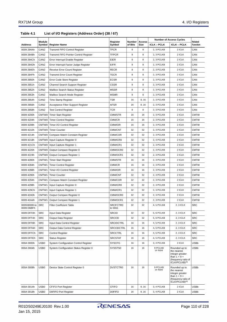
R01DS0249EJ0100 Rev.1.00 Page 110 of 228Jan 15, 2015
RX71M Group 4. I/O Registers
0009 284Ah CAN2 Transmit FIFO Control Register TFCR 8 8 2, 3 PCLKB 2 ICLK CAN
0009 284Bh CAN2 Transmit FIFO Pointer Control Register TFPCR 8 8 2, 3 PCLKB 2 ICLK CAN
0009 284Ch CAN2 Error Interrupt Enable Register EIER 8 8 2, 3 PCLKB 2 ICLK CAN
0009 284Dh CAN2 Error Interrupt Factor Judge Register EIFR 8 8 2, 3 PCLKB 2 ICLK CAN
0009 284Eh CAN2 Receive Error Count Register RECR 8 8 2, 3 PCLKB 2 ICLK CAN
0009 284Fh CAN2 Transmit Error Count Register TECR 8 8 2, 3 PCLKB 2 ICLK CAN
0009 2850h CAN2 Error Code Store Register ECSR 8 8 2, 3 PCLKB 2 ICLK CAN
0009 2851h CAN2 Channel Search Support Register CSSR 8 8 2, 3 PCLKB 2 ICLK CAN
0009 2852h CAN2 Mailbox Search Status Register MSSR 8 8 2, 3 PCLKB 2 ICLK CAN
0009 2853h CAN2 Mailbox Search Mode Register MSMR 8 8 2, 3 PCLKB 2 ICLK CAN
0009 2854h CAN2 Time Stamp Register TSR 16 8, 16 2, 3 PCLKB 2 ICLK CAN
0009 2856h CAN2 Acceptance Filter Support Register AFSR 16 8, 16 2, 3 PCLKB 2 ICLK CAN
0009 2858h CAN2 Test Control Register TCR 8 8 2, 3 PCLKB 2 ICLK CAN
0009 4200h CMTW0 Timer Start Register CMWSTR 16 16 2, 3 PCLKB 2 ICLK CMTW
0009 4204h CMTW0 Timer Control Register CMWCR 16 16 2, 3 PCLKB 2 ICLK CMTW
0009 4208h CMTW0 Timer I/O Control Register CMWIOR 16 16 2, 3 PCLKB 2 ICLK CMTW
0009 4210h CMTW0 Timer Counter CMWCNT 32 32 2, 3 PCLKB 2 ICLK CMTW
0009 4214h CMTW0 Compare Match Constant Register CMWCOR 32 32 2, 3 PCLKB 2 ICLK CMTW
0009 4218h CMTW0 Input Capture Register 0 CMWICR0 32 32 2, 3 PCLKB 2 ICLK CMTW
0009 421Ch CMTW0 Input Capture Register 1 CMWICR1 32 32 2, 3 PCLKB 2 ICLK CMTW
0009 4220h CMTW0 Output Compare Register 0 CMWOCR0 32 32 2, 3 PCLKB 2 ICLK CMTW
0009 4224h CMTW0 Output Compare Register 1 CMWOCR1 32 32 2, 3 PCLKB 2 ICLK CMTW
0009 4280h CMTW1 Timer Start Register CMWSTR 16 16 2, 3 PCLKB 2 ICLK CMTW
0009 4284h CMTW1 Timer Control Register CMWCR 16 16 2, 3 PCLKB 2 ICLK CMTW
0009 4288h CMTW1 Timer I/O Control Register CMWIOR 16 16 2, 3 PCLKB 2 ICLK CMTW
0009 4290h CMTW1 Timer Counter CMWCNT 32 32 2, 3 PCLKB 2 ICLK CMTW
0009 4294h CMTW1 Compare Match Constant Register CMWCOR 32 32 2, 3 PCLKB 2 ICLK CMTW
0009 4298h CMTW1 Input Capture Register 0 CMWICR0 32 32 2, 3 PCLKB 2 ICLK CMTW
0009 429Ch CMTW1 Input Capture Register 1 CMWICR1 32 32 2, 3 PCLKB 2 ICLK CMTW
0009 42A0h CMTW1 Output Compare Register 0 CMWOCR0 32 32 2, 3 PCLKB 2 ICLK CMTW
0009 42A4h CMTW1 Output Compare Register 1 CMWOCR1 32 32 2, 3 PCLKB 2 ICLK CMTW
0009 8000h to 0009 D6BFh
SRC Filter Coefficient Table SRCFCTR0 to 5551
32 32 4, 5 PCLKB 2, 3 ICLK SRC
0009 DFF0h SRC Input Data Register SRCID 32 32 5, 6 PCLKB 2, 3 ICLK SRC
0009 DFF4h SRC Output Data Register SRCOD 32 32 5, 6 PCLKB 2, 3 ICLK SRC
0009 DFF8h SRC Input Data Control Register SRCIDCTRL 16 16 4, 5 PCLKB 2, 3 ICLK SRC
0009 DFFAh SRC Output Data Control Register SRCODCTRL 16 16 4, 5 PCLKB 2, 3 ICLK SRC
0009 DFFCh SRC Control Register SRCCTRL 16 16 4, 5 PCLKB 2, 3 ICLK SRC
0009 DFFEh SRC Status Register SRCSTAT 16 16 4, 5 PCLKB 2, 3 ICLK SRC
000A 0000h USB0 System Configuration Control Register SYSCFG 16 16 3, 4 PCLKB 2 ICLK USBb
000A 0004h USB0 System Configuration Status Register 0 SYSSTS0 16 16 9 PCLKBor more
Rounded up to the nearest integer greater than 1 + 9 × (frequency ratio of ICLK/PCLKB)*5
USBb
000A 0008h USB0 Device State Control Register 0 DVSTCTR0 16 16 9 PCLKBor more
Rounded up to the nearest integer greater than 1 + 9 × (frequency ratio of ICLK/PCLKB)*5
USBb
000A 0014h USB0 CFIFO Port Register CFIFO 16 8, 16 3, 4 PCLKB 2 ICLK USBb
000A 0018h USB0 D0FIFO Port Register D0FIFO 16 8, 16 3, 4 PCLKB 2 ICLK USBb
Table 4.1 List of I/O Registers (Address Order) (38 / 67)
AddressModule Symbol Register Name
Register Symbol
Number of Bits
Access Size
Number of Access CyclesRelated Function ICLK PCLK ICLK PCLK

R01DS0249EJ0100 Rev.1.00 Page 111 of 228Jan 15, 2015
RX71M Group 4. I/O Registers
000A 001Ch USB0 D1FIFO Port Register D1FIFO 16 8, 16 3, 4 PCLKB 2 ICLK USBb
000A 0020h USB0 CFIFO Port Select Register CFIFOSEL 16 16 3, 4 PCLKB 2 ICLK USBb
000A 0022h USB0 CFIFO Port Control Register CFIFOCTR 16 16 3, 4 PCLKB 2 ICLK USBb
000A 0028h USB0 D0FIFO Port Select Register D0FIFOSEL 16 16 3, 4 PCLKB 2 ICLK USBb
000A 002Ah USB0 D0FIFO Port Control Register D0FIFOCTR 16 16 3, 4 PCLKB 2 ICLK USBb
000A 002Ch USB0 D1FIFO Port Select Register D1FIFOSEL 16 16 3, 4 PCLKB 2 ICLK USBb
000A 002Eh USB0 D1FIFO Port Control Register D1FIFOCTR 16 16 3, 4 PCLKB 2 ICLK USBb
000A 0030h USB0 Interrupt Enable Register 0 INTENB0 16 16 9 PCLKBor more
Frequency with 1 + 9 × (frequency ratio of ICLK/PCLKB)*5
USBb
000A 0032h USB0 Interrupt Enable Register 1 INTENB1 16 16 9 PCLKBor more
Frequency with 1 + 9 × (frequency ratio of ICLK/PCLKB)*5
USBb
000A 0036h USB0 BRDY Interrupt Enable Register BRDYENB 16 16 9 PCLKBor more
Frequency with 1 + 9 × (frequency ratio of ICLK/PCLKB)*5
USBb
000A 0038h USB0 NRDY Interrupt Enable Register NRDYENB 16 16 9 PCLKBor more
Frequency with 1 + 9 × (frequency ratio of ICLK/PCLKB)*5
USBb
000A 003Ah USB0 BEMP Interrupt Enable Register BEMPENB 16 16 9 PCLKBor more
Frequency with 1 + 9 × (frequency ratio of ICLK/PCLKB)*5
USBb
000A 003Ch USB0 SOF Output Configuration Register SOFCFG 16 16 9 PCLKBor more
Frequency with 1 + 9 × (frequency ratio of ICLK/PCLKB)*5
USBb
000A 0040h USB0 Interrupt Status Register 0 INTSTS0 16 16 9 PCLKBor more
Frequency with 1 + 9 × (frequency ratio of ICLK/PCLKB)*5
USBb
000A 0042h USB0 Interrupt Status Register 1 INTSTS1 16 16 9 PCLKBor more
Frequency with 1 + 9 × (frequency ratio of ICLK/PCLKB)*5
USBb
000A 0046h USB0 BRDY Interrupt Status Register BRDYSTS 16 16 9 PCLKBor more
Frequency with 1 + 9 × (frequency ratio of ICLK/PCLKB)*5
USBb
000A 0048h USB0 NRDY Interrupt Status Register NRDYSTS 16 16 9 PCLKBor more
Frequency with 1 + 9 × (frequency ratio of ICLK/PCLKB)*5
USBb
000A 004Ah USB0 BEMP Interrupt Status Register BEMPSTS 16 16 9 PCLKBor more
Frequency with 1 + 9 × (frequency ratio of ICLK/PCLKB)*5
USBb
000A 004Ch USB0 Frame Number Register FRMNUM 16 16 9 PCLKBor more
Frequency with 1 + 9 × (frequency ratio of ICLK/PCLKB)*5
USBb
000A 004Eh USB0 Device State Change Register DVCHGR 16 16 9 PCLKBor more
Frequency with 1 + 9 × (frequency ratio of ICLK/PCLKB)*5
USBb
000A 0050h USB0 USB Address Register USBADDR 16 16 9 PCLKBor more
Frequency with 1 + 9 × (frequency ratio of ICLK/PCLKB)*5
USBb
000A 0054h USB0 USB Request Type Register USBREQ 16 16 9 PCLKBor more
Frequency with 1 + 9 × (frequency ratio of ICLK/PCLKB)*5
USBb
Table 4.1 List of I/O Registers (Address Order) (39 / 67)
AddressModule Symbol Register Name
Register Symbol
Number of Bits
Access Size
Number of Access CyclesRelated Function ICLK PCLK ICLK PCLK

R01DS0249EJ0100 Rev.1.00 Page 112 of 228Jan 15, 2015
RX71M Group 4. I/O Registers
000A 0056h USB0 USB Request Value Register USBVAL 16 16 9 PCLKBor more
Frequency with 1 + 9 × (frequency ratio of ICLK/PCLKB)*5
USBb
000A 0058h USB0 USB Request Index Register USBINDX 16 16 9 PCLKBor more
Frequency with 1 + 9 × (frequency ratio of ICLK/PCLKB)*5
USBb
000A 005Ah USB0 USB Request Length Register USBLENG 16 16 9 PCLKBor more
Frequency with 1 + 9 × (frequency ratio of ICLK/PCLKB)*5
USBb
000A 005Ch USB0 DCP Configuration Register DCPCFG 16 16 9 PCLKBor more
Frequency with 1 + 9 × (frequency ratio of ICLK/PCLKB)*5
USBb
000A 005Eh USB0 DCP Maximum Packet Size Register DCPMAXP 16 16 9 PCLKBor more
Frequency with 1 + 9 × (frequency ratio of ICLK/PCLKB)*5
USBb
000A 0060h USB0 DCP Control Register DCPCTR 16 16 9 PCLKBor more
Frequency with 1 + 9 × (frequency ratio of ICLK/PCLKB)*5
USBb
000A 0064h USB0 Pipe Window Select Register PIPESEL 16 16 9 PCLKBor more
Frequency with 1 + 9 × (frequency ratio of ICLK/PCLKB)*5
USBb
000A 0068h USB0 Pipe Configuration Register PIPECFG 16 16 9 PCLKBor more
Frequency with 1 + 9 × (frequency ratio of ICLK/PCLKB)*5
USBb
000A 006Ch USB0 Pipe Maximum Packet Size Register PIPEMAXP 16 16 9 PCLKBor more
Frequency with 1 + 9 × (frequency ratio of ICLK/PCLKB)*5
USBb
000A 006Eh USB0 Pipe Cycle Control Register PIPEPERI 16 16 9 PCLKBor more
Frequency with 1 + 9 × (frequency ratio of ICLK/PCLKB)*5
USBb
000A 0070h USB0 Pipe1 Control Register PIPE1CTR 16 16 9 PCLKBor more
Frequency with 1 + 9 × (frequency ratio of ICLK/PCLKB)*5
USBb
000A 0072h USB0 Pipe2 Control Register PIPE2CTR 16 16 9 PCLKBor more
Frequency with 1 + 9 × (frequency ratio of ICLK/PCLKB)*5
USBb
000A 0074h USB0 Pipe3 Control Register PIPE3CTR 16 16 9 PCLKBor more
Frequency with 1 + 9 × (frequency ratio of ICLK/PCLKB)*5
USBb
000A 0076h USB0 Pipe4 Control Register PIPE4CTR 16 16 9 PCLKBor more
Frequency with 1 + 9 × (frequency ratio of ICLK/PCLKB)*5
USBb
000A 0078h USB0 Pipe5 Control Register PIPE5CTR 16 16 9 PCLKBor more
Frequency with 1 + 9 × (frequency ratio of ICLK/PCLKB)*5
USBb
000A 007Ah USB0 Pipe6 Control Register PIPE6CTR 16 16 9 PCLKBor more
Frequency with 1 + 9 × (frequency ratio of ICLK/PCLKB)*5
USBb
000A 007Ch USB0 Pipe7 Control Register PIPE7CTR 16 16 9 PCLKBor more
Frequency with 1 + 9 × (frequency ratio of ICLK/PCLKB)*5
USBb
000A 007Eh USB0 Pipe8 Control Register PIPE8CTR 16 16 9 PCLKBor more
Frequency with 1 + 9 × (frequency ratio of ICLK/PCLKB)*5
USBb
Table 4.1 List of I/O Registers (Address Order) (40 / 67)
AddressModule Symbol Register Name
Register Symbol
Number of Bits
Access Size
Number of Access CyclesRelated Function ICLK PCLK ICLK PCLK

R01DS0249EJ0100 Rev.1.00 Page 113 of 228Jan 15, 2015
RX71M Group 4. I/O Registers
000A 0080h USB0 Pipe9 Control Register PIPE9CTR 16 16 9 PCLKBor more
Frequency with 1 + 9 × (frequency ratio of ICLK/PCLKB)*5
USBb
000A 0090h USB0 Pipe1 Transaction Counter Enable Register PIPE1TRE 16 16 9 PCLKBor more
Frequency with 1 + 9 × (frequency ratio of ICLK/PCLKB)*5
USBb
000A 0092h USB0 Pipe1 Transaction Counter Register PIPE1TRN 16 16 9 PCLKBor more
Frequency with 1 + 9 × (frequency ratio of ICLK/PCLKB)*5
USBb
000A 0094h USB0 Pipe2 Transaction Counter Enable Register PIPE2TRE 16 16 9 PCLKBor more
Frequency with 1 + 9 × (frequency ratio of ICLK/PCLKB)*5
USBb
000A 0096h USB0 Pipe2 Transaction Counter Register PIPE2TRN 16 16 9 PCLKBor more
Frequency with 1 + 9 × (frequency ratio of ICLK/PCLKB)*5
USBb
000A 0098h USB0 Pipe3 Transaction Counter Enable Register PIPE3TRE 16 16 9 PCLKBor more
Frequency with 1 + 9 × (frequency ratio of ICLK/PCLKB)*5
USBb
000A 009Ah USB0 Pipe3 Transaction Counter Register PIPE3TRN 16 16 9 PCLKBor more
Frequency with 1 + 9 × (frequency ratio of ICLK/PCLKB)*5
USBb
000A 009Ch USB0 Pipe4 Transaction Counter Enable Register PIPE4TRE 16 16 9 PCLKBor more
Frequency with 1 + 9 × (frequency ratio of ICLK/PCLKB)*5
USBb
000A 009Eh USB0 Pipe4 Transaction Counter Register PIPE4TRN 16 16 9 PCLKBor more
Frequency with 1 + 9 × (frequency ratio of ICLK/PCLKB)*5
USBb
000A 00A0h USB0 Pipe5 Transaction Counter Enable Register PIPE5TRE 16 16 9 PCLKBor more
Frequency with 1 + 9 × (frequency ratio of ICLK/PCLKB)*5
USBb
000A 00A2h USB0 Pipe5 Transaction Counter Register PIPE5TRN 16 16 9 PCLKBor more
Frequency with 1 + 9 × (frequency ratio of ICLK/PCLKB)*5
USBb
000A 00D0h USB0 Device Address 0 Configuration Register DEVADD0 16 16 9 PCLKBor more
Frequency with 1 + 9 × (frequency ratio of ICLK/PCLKB)*5
USBb
000A 00D2h USB0 Device Address 1 Configuration Register DEVADD1 16 16 9 PCLKBor more
Frequency with 1 + 9 × (frequency ratio of ICLK/PCLKB)*5
USBb
000A 00D4h USB0 Device Address 2 Configuration Register DEVADD2 16 16 9 PCLKBor more
Frequency with 1 + 9 × (frequency ratio of ICLK/PCLKB)*5
USBb
000A 00D6h USB0 Device Address 3 Configuration Register DEVADD3 16 16 9 PCLKBor more
Frequency with 1 + 9 × (frequency ratio of ICLK/PCLKB)*5
USBb
000A 00D8h USB0 Device Address 4 Configuration Register DEVADD4 16 16 9 PCLKBor more
Frequency with 1 + 9 × (frequency ratio of ICLK/PCLKB)*5
USBb
000A 00DAh USB0 Device Address 5 Configuration Register DEVADD5 16 16 9 PCLKBor more
Frequency with 1 + 9 × (frequency ratio of ICLK/PCLKB)*5
USBb
000A 00F0h USB0 PHY Cross Point Adjustment Register PHYSLEW 32 32 9 PCLKBor more
Frequency with 1 + 9 × (frequency ratio of ICLK/PCLKB)*5
USBb
Table 4.1 List of I/O Registers (Address Order) (41 / 67)
AddressModule Symbol Register Name
Register Symbol
Number of Bits
Access Size
Number of Access CyclesRelated Function ICLK PCLK ICLK PCLK

R01DS0249EJ0100 Rev.1.00 Page 114 of 228Jan 15, 2015
RX71M Group 4. I/O Registers
000A 0400h USB Deep Standby USB Transceiver Control/Pin Monitoring Register
DPUSR0R 32 32 9 PCLKBor more
Frequency with 1 + 9 × (frequency ratio of ICLK/PCLKB)*5
USBb
000A 0404h USB Deep Standby USB Suspend/Resume Interrupt Register
DPUSR1R 32 32 9 PCLKBor more
Frequency with 1 + 9 × (frequency ratio of ICLK/PCLKB)*5
USBb
000A 0500h PDC PDC Control Register 0 PCCR0 32 32 2, 3 PCLKB 2 ICLK PDC
000A 0504h PDC PDC Control Register 1 PCCR1 32 32 2, 3 PCLKB 2 ICLK PDC
000A 0508h PDC PDC Status Register PCSR 32 32 2, 3 PCLKB 2 ICLK PDC
000A 050Ch PDC PDC Pin Monitor Register PCMONR 32 32 2, 3 PCLKB 2 ICLK PDC
000A 0510h PDC PDC Receive Data Register PCDR 32 32 2, 3 PCLKB 2 ICLK PDC
000A 0514h PDC Vertical Capture Register VCR 32 32 2, 3 PCLKB 2 ICLK PDC
000A 0518h PDC Horizontal Capture Register HCR 32 32 2, 3 PCLKB 2 ICLK PDC
000C 0000h EDMAC0
EDMAC Mode Register EDMR 32 32 4, 5 PCLKA 2, 3 ICLK EDMACa
000C 0008h EDMAC0
EDMAC Transmit Request Register EDTRR 32 32 4, 5 PCLKA 2, 3 ICLK EDMACa
000C 0010h EDMAC0
EDMAC Receive Request Register EDRRR 32 32 4, 5 PCLKA 2, 3 ICLK EDMACa
000C 0018h EDMAC0
Transmit Descriptor List Start Address Register TDLAR 32 32 4, 5 PCLKA 2, 3 ICLK EDMACa
000C 0020h EDMAC0
Receive Descriptor List Start Address Register RDLAR 32 32 4, 5 PCLKA 2, 3 ICLK EDMACa
000C 0028h EDMAC0
ETHERC/EDMAC Status Register EESR 32 32 4, 5 PCLKA 2, 3 ICLK EDMACa
000C 0030h EDMAC0
ETHERC/EDMAC Status Interrupt Enable Register EESIPR 32 32 4, 5 PCLKA 2, 3 ICLK EDMACa
000C 0038h EDMAC0
ETHERC/EDMAC Transmit/Receive Status Copy Enable Register
TRSCER 32 32 4, 5 PCLKA 2, 3 ICLK EDMACa
000C 0040h EDMAC0
Missed-Frame Counter Register RMFCR 32 32 4, 5 PCLKA 2, 3 ICLK EDMACa
000C 0048h EDMAC0
Transmit FIFO Threshold Register TFTR 32 32 4, 5 PCLKA 2, 3 ICLK EDMACa
000C 0050h EDMAC0
FIFO Depth Register FDR 32 32 4, 5 PCLKA 2, 3 ICLK EDMACa
000C 0058h EDMAC0
Receive Method Control Register RMCR 32 32 4, 5 PCLKA 2, 3 ICLK EDMACa
000C 0064h EDMAC0
Transmit FIFO Underflow Counter TFUCR 32 32 4, 5 PCLKA 2, 3 ICLK EDMACa
000C 0068h EDMAC0
Receive FIFO Overflow Counter RFOCR 32 32 4, 5 PCLKA 2, 3 ICLK EDMACa
000C 006Ch EDMAC0
Independent Output Signal Setting Register IOSR 32 32 4, 5 PCLKA 2, 3 ICLK EDMACa
000C 0070h EDMAC0
Flow Control Start FIFO Threshold Setting Register FCFTR 32 32 4, 5 PCLKA 2, 3 ICLK EDMACa
000C 0078h EDMAC0
Receive Data Padding Insert Register RPADIR 32 32 4, 5 PCLKA 2, 3 ICLK EDMACa
000C 007Ch EDMAC0
Transmit Interrupt Setting Register TRIMD 32 32 4, 5 PCLKA 2, 3 ICLK EDMACa
000C 00C8h EDMAC0
Receive Buffer Write Address Register RBWAR 32 32 4, 5 PCLKA 2, 3 ICLK EDMACa
000C 00CCh EDMAC0
Receive Descriptor Fetch Address Register RDFAR 32 32 4, 5 PCLKA 2, 3 ICLK EDMACa
000C 00D4h EDMAC0
Transmit Buffer Read Address Register TBRAR 32 32 4, 5 PCLKA 2, 3 ICLK EDMACa
000C 00D8h EDMAC0
Transmit Descriptor Fetch Address Register TDFAR 32 32 4, 5 PCLKA 2, 3 ICLK EDMACa
000C 0100h ETHERC0
ETHERC Mode Register ECMR 32 32 13, 14 PCLKA 2 to 7 ICLK ETHERC
000C 0108h ETHERC0
Receive Frame Length Register RFLR 32 32 13, 14 PCLKA 2 to 7 ICLK ETHERC
Table 4.1 List of I/O Registers (Address Order) (42 / 67)
AddressModule Symbol Register Name
Register Symbol
Number of Bits
Access Size
Number of Access CyclesRelated Function ICLK PCLK ICLK PCLK

R01DS0249EJ0100 Rev.1.00 Page 115 of 228Jan 15, 2015
RX71M Group 4. I/O Registers
000C 0110h ETHERC0
ETHERC Status Register ECSR 32 32 13, 14 PCLKA 2 to 7 ICLK ETHERC
000C 0118h ETHERC0
ETHERC Interrupt Enable Register ECSIPR 32 32 13, 14 PCLKA 2 to 7 ICLK ETHERC
000C 0120h ETHERC0
PHY Interface Register PIR 32 32 13, 14 PCLKA 2 to 7 ICLK ETHERC
000C 0128h ETHERC0
PHY Status Register PSR 32 32 13, 14 PCLKA 2 to 7 ICLK ETHERC
000C 0140h ETHERC0
Random Number Generation Counter Upper Limit Setting Register
RDMLR 32 32 13, 14 PCLKA 2 to 7 ICLK ETHERC
000C 0150h ETHERC0
IPG Register IPGR 32 32 13, 14 PCLKA 2 to 7 ICLK ETHERC
000C 0154h ETHERC0
Automatic PAUSE Frame Register APR 32 32 13, 14 PCLKA 2 to 7 ICLK ETHERC
000C 0158h ETHERC0
Manual PAUSE Frame Register MPR 32 32 13, 14 PCLKA 2 to 7 ICLK ETHERC
000C 0160h ETHERC0
Received PAUSE Frame Counter RFCF 32 32 13, 14 PCLKA 2 to 7 ICLK ETHERC
000C 0164h ETHERC0
PAUSE Frame Retransmit Count Setting Register TPAUSER 32 32 13, 14 PCLKA 2 to 7 ICLK ETHERC
000C 0168h ETHERC0
PAUSE Frame Retransmit Counter TPAUSECR 32 32 13, 14 PCLKA 2 to 7 ICLK ETHERC
000C 016Ch ETHERC0
Broadcast Frame Receive Count Setting Register BCFRR 32 32 13, 14 PCLKA 2 to 7 ICLK ETHERC
000C 01C0h ETHERC0
MAC Address Upper Bit Register MAHR 32 32 13, 14 PCLKA 2 to 7 ICLK ETHERC
000C 01C8h ETHERC0
MAC Address Lower Bit Register MALR 32 32 13, 14 PCLKA 2 to 7 ICLK ETHERC
000C 01D0h ETHERC0
Transmit Retry Over Counter Register TROCR 32 32 13, 14 PCLKA 2 to 7 ICLK ETHERC
000C 01D4h ETHERC0
Late Collision Detect Counter Register CDCR 32 32 13, 14 PCLKA 2 to 7 ICLK ETHERC
000C 01D8h ETHERC0
Lost Carrier Counter Register LCCR 32 32 13, 14 PCLKA 2 to 7 ICLK ETHERC
000C 01DCh ETHERC0
Carrier Not Detect Counter Register CNDCR 32 32 13, 14 PCLKA 2 to 7 ICLK ETHERC
000C 01E4h ETHERC0
CRC Error Frame Receive Counter Register CEFCR 32 32 13, 14 PCLKA 2 to 7 ICLK ETHERC
000C 01E8h ETHERC0
Frame Receive Error Counter Register FRECR 32 32 13, 14 PCLKA 2 to 7 ICLK ETHERC
000C 01ECh ETHERC0
Too-Short Frame Receive Counter Register TSFRCR 32 32 13, 14 PCLKA 2 to 7 ICLK ETHERC
000C 01F0h ETHERC0
Too-Long Frame Receive Counter Register TLFRCR 32 32 13, 14 PCLKA 2 to 7 ICLK ETHERC
000C 01F4h ETHERC0
Received Alignment Error Frame Counter Register RFCR 32 32 13, 14 PCLKA 2 to 7 ICLK ETHERC
000C 01F8h ETHERC0
Multicast Address Frame Receive Counter Register MAFCR 32 32 13, 14 PCLKA 2 to 7 ICLK ETHERC
000C 0200h EDMAC1
EDMAC Mode Register EDMR 32 32 4, 5 PCLKA 2, 3 ICLK EDMACa
000C 0208h EDMAC1
EDMAC Transmit Request Register EDTRR 32 32 4, 5 PCLKA 2, 3 ICLK EDMACa
000C 0210h EDMAC1
EDMAC Receive Request Register EDRRR 32 32 4, 5 PCLKA 2, 3 ICLK EDMACa
000C 0218h EDMAC1
Transmit Descriptor List Start Address Register TDLAR 32 32 4, 5 PCLKA 2, 3 ICLK EDMACa
000C 0220h EDMAC1
Receive Descriptor List Start Address Register RDLAR 32 32 4, 5 PCLKA 2, 3 ICLK EDMACa
000C 0228h EDMAC1
ETHERC/EDMAC Status Register EESR 32 32 4, 5 PCLKA 2, 3 ICLK EDMACa
000C 0230h EDMAC1
ETHERC/EDMAC Status Interrupt Enable Register EESIPR 32 32 4, 5 PCLKA 2, 3 ICLK EDMACa
Table 4.1 List of I/O Registers (Address Order) (43 / 67)
AddressModule Symbol Register Name
Register Symbol
Number of Bits
Access Size
Number of Access CyclesRelated Function ICLK PCLK ICLK PCLK

R01DS0249EJ0100 Rev.1.00 Page 116 of 228Jan 15, 2015
RX71M Group 4. I/O Registers
000C 0238h EDMAC1
ETHERC/EDMAC Transmit/Receive Status Copy Enable Register
TRSCER 32 32 4, 5 PCLKA 2, 3 ICLK EDMACa
000C 0240h EDMAC1
Missed-Frame Counter Register RMFCR 32 32 4, 5 PCLKA 2, 3 ICLK EDMACa
000C 0248h EDMAC1
Transmit FIFO Threshold Register TFTR 32 32 4, 5 PCLKA 2, 3 ICLK EDMACa
000C 0250h EDMAC1
FIFO Depth Register FDR 32 32 4, 5 PCLKA 2, 3 ICLK EDMACa
000C 0258h EDMAC1
Receive Method Control Register RMCR 32 32 4, 5 PCLKA 2, 3 ICLK EDMACa
000C 0264h EDMAC1
Transmit FIFO Underflow Counter TFUCR 32 32 4, 5 PCLKA 2, 3 ICLK EDMACa
000C 0268h EDMAC1
Receive FIFO Overflow Counter RFOCR 32 32 4, 5 PCLKA 2, 3 ICLK EDMACa
000C 026Ch EDMAC1
Independent Output Signal Setting Register IOSR 32 32 4, 5 PCLKA 2, 3 ICLK EDMACa
000C 0270h EDMAC1
Flow Control Start FIFO Threshold Setting Register FCFTR 32 32 4, 5 PCLKA 2, 3 ICLK EDMACa
000C 0278h EDMAC1
Receive Data Padding Insert Register RPADIR 32 32 4, 5 PCLKA 2, 3 ICLK EDMACa
000C 027Ch EDMAC1
Transmit Interrupt Setting Register TRIMD 32 32 4, 5 PCLKA 2, 3 ICLK EDMACa
000C 02C8h EDMAC1
Receive Buffer Write Address Register RBWAR 32 32 4, 5 PCLKA 2, 3 ICLK EDMACa
000C 02CCh EDMAC1
Receive Descriptor Fetch Address Register RDFAR 32 32 4, 5 PCLKA 2, 3 ICLK EDMACa
000C 02D4h EDMAC1
Transmit Buffer Read Address Register TBRAR 32 32 4, 5 PCLKA 2, 3 ICLK EDMACa
000C 02D8h EDMAC1
Transmit Descriptor Fetch Address Register TDFAR 32 32 4, 5 PCLKA 2, 3 ICLK EDMACa
000C 0300h ETHERC1
ETHERC Mode Register ECMR 32 32 13, 14 PCLKA 2 to 7 ICLK ETHERC
000C 0308h ETHERC1
Receive Frame Length Register RFLR 32 32 13, 14 PCLKA 2 to 7 ICLK ETHERC
000C 0310h ETHERC1
ETHERC Status Register ECSR 32 32 13, 14 PCLKA 2 to 7 ICLK ETHERC
000C 0318h ETHERC1
ETHERC Interrupt Enable Register ECSIPR 32 32 13, 14 PCLKA 2 to 7 ICLK ETHERC
000C 0320h ETHERC1
PHY Interface Register PIR 32 32 13, 14 PCLKA 2 to 7 ICLK ETHERC
000C 0328h ETHERC1
PHY Status Register PSR 32 32 13, 14 PCLKA 2 to 7 ICLK ETHERC
000C 0340h ETHERC1
Random Number Generation Counter Upper Limit Setting Register
RDMLR 32 32 13, 14 PCLKA 2 to 7 ICLK ETHERC
000C 0350h ETHERC1
IPG Register IPGR 32 32 13, 14 PCLKA 2 to 7 ICLK ETHERC
000C 0354h ETHERC1
Automatic PAUSE Frame Register APR 32 32 13, 14 PCLKA 2 to 7 ICLK ETHERC
000C 0358h ETHERC1
Manual PAUSE Frame Register MPR 32 32 13, 14 PCLKA 2 to 7 ICLK ETHERC
000C 0360h ETHERC1
Received PAUSE Frame Counter RFCF 32 32 13, 14 PCLKA 2 to 7 ICLK ETHERC
000C 0364h ETHERC1
PAUSE Frame Retransmit Count Setting Register TPAUSER 32 32 13, 14 PCLKA 2 to 7 ICLK ETHERC
000C 0368h ETHERC1
PAUSE Frame Retransmit Counter Register TPAUSECR 32 32 13, 14 PCLKA 2 to 7 ICLK ETHERC
000C 036Ch ETHERC1
Broadcast Frame Receive Count Setting Register BCFRR 32 32 13, 14 PCLKA 2 to 7 ICLK ETHERC
000C 03C0h ETHERC1
MAC Address Upper Bit Register MAHR 32 32 13, 14 PCLKA 2 to 7 ICLK ETHERC
000C 03C8h ETHERC1
MAC Address Lower Bit Register MALR 32 32 13, 14 PCLKA 2 to 7 ICLK ETHERC
Table 4.1 List of I/O Registers (Address Order) (44 / 67)
AddressModule Symbol Register Name
Register Symbol
Number of Bits
Access Size
Number of Access CyclesRelated Function ICLK PCLK ICLK PCLK

R01DS0249EJ0100 Rev.1.00 Page 117 of 228Jan 15, 2015
RX71M Group 4. I/O Registers
000C 03D0h ETHERC1
Transmit Retry Over Counter Register TROCR 32 32 13, 14 PCLKA 2 to 7 ICLK ETHERC
000C 03D4h ETHERC1
Late Collision Detect Counter Register CDCR 32 32 13, 14 PCLKA 2 to 7 ICLK ETHERC
000C 03D8h ETHERC1
Lost Carrier Counter Register LCCR 32 32 13, 14 PCLKA 2 to 7 ICLK ETHERC
000C 03DCh ETHERC1
Carrier Not Detect Counter Register CNDCR 32 32 13, 14 PCLKA 2 to 7 ICLK ETHERC
000C 03E4h ETHERC1
CRC Error Frame Receive Counter Register CEFCR 32 32 13, 14 PCLKA 2 to 7 ICLK ETHERC
000C 03E8h ETHERC1
Frame Receive Error Counter Register FRECR 32 32 13, 14 PCLKA 2 to 7 ICLK ETHERC
000C 03ECh ETHERC1
Too-Short Frame Receive Counter Register TSFRCR 32 32 13, 14 PCLKA 2 to 7 ICLK ETHERC
000C 03F0h ETHERC1
Too-Long Frame Receive Counter Register TLFRCR 32 32 13, 14 PCLKA 2 to 7 ICLK ETHERC
000C 03F4h ETHERC1
Received Alignment Error Frame Counter Register RFCR 32 32 13, 14 PCLKA 2 to 7 ICLK ETHERC
000C 03F8h ETHERC1
Multicast Address Frame Receive Counter Register MAFCR 32 32 13, 14 PCLKA 2 to 7 ICLK ETHERC
000C 0400h PTPEDMAC
EDMAC Mode Register EDMR 32 32 4, 5 PCLKA 2, 3 ICLK EDMACa
000C 0408h PTPEDMAC
EDMAC Transmit Request Register EDTRR 32 32 4, 5 PCLKA 2, 3 ICLK EDMACa
000C 0410h PTPEDMAC
EDMAC Receive Request Register EDRRR 32 32 4, 5 PCLKA 2, 3 ICLK EDMACa
000C 0418h PTPEDMAC
Transmit Descriptor List Start Address Register TDLAR 32 32 4, 5 PCLKA 2, 3 ICLK EDMACa
000C 0420h PTPEDMAC
Receive Descriptor List Start Address Register RDLAR 32 32 4, 5 PCLKA 2, 3 ICLK EDMACa
000C 0428h PTPEDMAC
PTP/EDMAC Status Register EESR 32 32 4, 5 PCLKA 2, 3 ICLK EDMACa
000C 0430h PTPEDMAC
PTP/EDMAC Status Interrupt Enable Register EESIPR 32 32 4, 5 PCLKA 2, 3 ICLK EDMACa
000C 0440h PTPEDMAC
Missed-Frame Counter Register RMFCR 32 32 4, 5 PCLKA 2, 3 ICLK EDMACa
000C 0448h PTPEDMAC
Transmit FIFO Threshold Register TFTR 32 32 4, 5 PCLKA 2, 3 ICLK EDMACa
000C 0450h PTPEDMAC
FIFO Depth Register FDR 32 32 4, 5 PCLKA 2, 3 ICLK EDMACa
000C 0458h PTPEDMAC
Receive Method Control Register RMCR 32 32 4, 5 PCLKA 2, 3 ICLK EDMACa
000C 0464h PTPEDMAC
Transmit FIFO Underflow Counter TFUCR 32 32 4, 5 PCLKA 2, 3 ICLK EDMACa
000C 0468h PTPEDMAC
Receive FIFO Overflow Counter RFOCR 32 32 4, 5 PCLKA 2, 3 ICLK EDMACa
000C 0470h PTPEDMAC
Flow Control Start FIFO Threshold Setting Register FCFTR 32 32 4, 5 PCLKA 2, 3 ICLK EDMACa
000C 0478h PTPEDMAC
Receive Data Padding Insert Register RPADIR 32 32 4, 5 PCLKA 2, 3 ICLK EDMACa
000C 047Ch PTPEDMAC
Transmit Interrupt Setting Register TRIMD 32 32 4, 5 PCLKA 2, 3 ICLK EDMACa
000C 04C8h PTPEDMAC
Receive Buffer Write Address Register RBWAR 32 32 4, 5 PCLKA 2, 3 ICLK EDMACa
000C 04CCh PTPEDMAC
Receive Descriptor Fetch Address Register RDFAR 32 32 4, 5 PCLKA 2, 3 ICLK EDMACa
000C 04D4h PTPEDMAC
Transmit Buffer Read Address Register TBRAR 32 32 4, 5 PCLKA 2, 3 ICLK EDMACa
000C 04D8h PTPEDMAC
Transmit Descriptor Fetch Address Register TDFAR 32 32 4, 5 PCLKA 2, 3 ICLK EDMACa
000C 0500h EPTPC PTP Reset Register PTRSTR 32 32 3, 4 PCLKA 2, 3 ICLK EPTPCa
000C 0504h EPTPC STCA Clock Select Register STCSELR 32 32 3, 4 PCLKA 2, 3 ICLK EPTPCa
000C 1200h MTU3 Timer Control Register TCR 8 8 5, 6 PCLKA 2, 3 ICLK MTU3a
Table 4.1 List of I/O Registers (Address Order) (45 / 67)
AddressModule Symbol Register Name
Register Symbol
Number of Bits
Access Size
Number of Access CyclesRelated Function ICLK PCLK ICLK PCLK

R01DS0249EJ0100 Rev.1.00 Page 118 of 228Jan 15, 2015
RX71M Group 4. I/O Registers
000C 1201h MTU4 Timer Control Register TCR 8 8 5, 6 PCLKA 2, 3 ICLK MTU3a
000C 1202h MTU3 Timer Mode Register 1 TMDR1 8 8 5, 6 PCLKA 2, 3 ICLK MTU3a
000C 1203h MTU4 Timer Mode Register 1 TMDR1 8 8 5, 6 PCLKA 2, 3 ICLK MTU3a
000C 1204h MTU3 Timer I/O Control Register H TIORH 8 8 5, 6 PCLKA 2, 3 ICLK MTU3a
000C 1205h MTU3 Timer I/O Control Register L TIORL 8 8 5, 6 PCLKA 2, 3 ICLK MTU3a
000C 1206h MTU4 Timer I/O Control Register H TIORH 8 8 5, 6 PCLKA 2, 3 ICLK MTU3a
000C 1207h MTU4 Timer I/O Control Register L TIORL 8 8 5, 6 PCLKA 2, 3 ICLK MTU3a
000C 1208h MTU3 Timer Interrupt Enable Register TIER 8 8 5, 6 PCLKA 2, 3 ICLK MTU3a
000C 1209h MTU4 Timer Interrupt Enable Register TIER 8 8 5, 6 PCLKA 2, 3 ICLK MTU3a
000C 120Ah MTU Timer Output Master Enable Register A TOERA 8 8 5, 6 PCLKA 2, 3 ICLK MTU3a
000C 120Dh MTU Timer Gate Control Register A TGCRA 8 8 5, 6 PCLKA 2, 3 ICLK MTU3a
000C 120Eh MTU Timer Output Control Register 1A TOCR1A 8 8 5, 6 PCLKA 2, 3 ICLK MTU3a
000C 120Fh MTU Timer Output Control Register 2A TOCR2A 8 8 5, 6 PCLKA 2, 3 ICLK MTU3a
000C 1210h MTU3 Timer Counter TCNT 16 16 5, 6 PCLKA 2, 3 ICLK MTU3a
000C 1212h MTU4 Timer Counter TCNT 16 16 5, 6 PCLKA 2, 3 ICLK MTU3a
000C 1214h MTU Timer Cycle Data Register A TCDRA 16 16 5, 6 PCLKA 2, 3 ICLK MTU3a
000C 1216h MTU Timer Dead Time Data Register A TDDRA 16 16 5, 6 PCLKA 2, 3 ICLK MTU3a
000C 1218h MTU3 Timer General Register A TGRA 16 16 5, 6 PCLKA 2, 3 ICLK MTU3a
000C 121Ah MTU3 Timer General Register B TGRB 16 16 5, 6 PCLKA 2, 3 ICLK MTU3a
000C 121Ch MTU4 Timer General Register A TGRA 16 16 5, 6 PCLKA 2, 3 ICLK MTU3a
000C 121Eh MTU4 Timer General Register B TGRB 16 16 5, 6 PCLKA 2, 3 ICLK MTU3a
000C 1220h MTU Timer Subcounter A TCNTSA 16 16 5, 6 PCLKA 2, 3 ICLK MTU3a
000C 1222h MTU Timer Cycle Buffer Register A TCBRA 16 16 5, 6 PCLKA 2, 3 ICLK MTU3a
000C 1224h MTU3 Timer General Register C TGRC 16 16 5, 6 PCLKA 2, 3 ICLK MTU3a
000C 1226h MTU3 Timer General Register D TGRD 16 16 5, 6 PCLKA 2, 3 ICLK MTU3a
000C 1228h MTU4 Timer General Register C TGRC 16 16 5, 6 PCLKA 2, 3 ICLK MTU3a
000C 122Ah MTU4 Timer General Register D TGRD 16 16 5, 6 PCLKA 2, 3 ICLK MTU3a
000C 122Ch MTU3 Timer Status Register TSR 8 8 5, 6 PCLKA 2, 3 ICLK MTU3a
000C 122Dh MTU4 Timer Status Register TSR 8 8 5, 6 PCLKA 2, 3 ICLK MTU3a
000C 1230h MTU Timer Interrupt Skipping Set Register 1A TITCR1A 8 8 5, 6 PCLKA 2, 3 ICLK MTU3a
000C 1231h MTU Timer Interrupt Skipping Counter 1A TITCNT1A 8 8 5, 6 PCLKA 2, 3 ICLK MTU3a
000C 1232h MTU Timer Buffer Transfer Set Register A TBTERA 8 8 5, 6 PCLKA 2, 3 ICLK MTU3a
000C 1234h MTU Timer Dead Time Enable Register A TDERA 8 8 5, 6 PCLKA 2, 3 ICLK MTU3a
000C 1236h MTU Timer Output Level Buffer Register A TOLBRA 8 8 5, 6 PCLKA 2, 3 ICLK MTU3a
000C 1238h MTU3 Timer Buffer Operation Transfer Mode Register TBTM 8 8 5, 6 PCLKA 2, 3 ICLK MTU3a
000C 1239h MTU4 Timer Buffer Operation Transfer Mode Register TBTM 8 8 5, 6 PCLKA 2, 3 ICLK MTU3a
000C 123Ah MTU Timer Interrupt Skipping Mode Register A TITMRA 8 8 5, 6 PCLKA 2, 3 ICLK MTU3a
000C 123Bh MTU Timer Interrupt Skipping Set Register 2A TITCR2A 8 8 5, 6 PCLKA 2, 3 ICLK MTU3a
000C 123Ch MTU Timer Interrupt Skipping Counter 2A TITCNT2A 8 8 5, 6 PCLKA 2, 3 ICLK MTU3a
000C 1240h MTU4 Timer A/D Converter Start Request Control Register TADCR 16 16 5, 6 PCLKA 2, 3 ICLK MTU3a
000C 1244h MTU4 Timer A/D Converter Start Request Cycle Set Register A
TADCORA 16 16 5, 6 PCLKA 2, 3 ICLK MTU3a
000C 1246h MTU4 Timer A/D Converter Start Request Cycle Set Register B
TADCORB 16 16 5, 6 PCLKA 2, 3 ICLK MTU3a
000C 1248h MTU4 Timer A/D Converter Start Request Cycle Set Buffer Register A
TADCOBRA 16 16 5, 6 PCLKA 2, 3 ICLK MTU3a
000C 124Ah MTU4 Timer A/D Converter Start Request Cycle Set Buffer Register B
TADCOBRB 16 16 5, 6 PCLKA 2, 3 ICLK MTU3a
000C 124Ch MTU3 Timer Control Register 2 TCR2 8 8 5, 6 PCLKA 2, 3 ICLK MTU3a
000C 124Dh MTU4 Timer Control Register 2 TCR2 8 8 5, 6 PCLKA 2, 3 ICLK MTU3a
000C 1260h MTU Timer Waveform Control Register A TWCRA 8 8 5, 6 PCLKA 2, 3 ICLK MTU3a
Table 4.1 List of I/O Registers (Address Order) (46 / 67)
AddressModule Symbol Register Name
Register Symbol
Number of Bits
Access Size
Number of Access CyclesRelated Function ICLK PCLK ICLK PCLK

R01DS0249EJ0100 Rev.1.00 Page 119 of 228Jan 15, 2015
RX71M Group 4. I/O Registers
000C 1270h MTU Timer Mode Register 2A TMDR2A 8 8 5, 6 PCLKA 2, 3 ICLK MTU3a
000C 1272h MTU3 Timer General Register E TGRE 16 16 5, 6 PCLKA 2, 3 ICLK MTU3a
000C 1274h MTU4 Timer General Register E TGRE 16 16 5, 6 PCLKA 2, 3 ICLK MTU3a
000C 1276h MTU4 Timer General Register F TGRF 16 16 5, 6 PCLKA 2, 3 ICLK MTU3a
000C 1280h MTU Timer Start Register A TSTRA 8 8 5, 6 PCLKA 2, 3 ICLK MTU3a
000C 1281h MTU Timer Synchronous Register A TSYRA 8 8 5, 6 PCLKA 2, 3 ICLK MTU3a
000C 1282h MTU Timer Counter Synchronous Start Register TCSYSTR 8 8 5, 6 PCLKA 2, 3 ICLK MTU3a
000C 1284h MTU Timer Read/Write Enable Register A TRWERA 8 8 5, 6 PCLKA 2, 3 ICLK MTU3a
000C 1290h MTU0 Noise Filter Control Register 0 NFCR0 8 8 5, 6 PCLKA 2, 3 ICLK MTU3a
000C 1291h MTU1 Noise Filter Control Register 1 NFCR1 8 8 5, 6 PCLKA 2, 3 ICLK MTU3a
000C 1292h MTU2 Noise Filter Control Register 2 NFCR2 8 8 5, 6 PCLKA 2, 3 ICLK MTU3a
000C 1293h MTU3 Noise Filter Control Register 3 NFCR3 8 8 5, 6 PCLKA 2, 3 ICLK MTU3a
000C 1294h MTU4 Noise Filter Control Register 4 NFCR4 8 8 5, 6 PCLKA 2, 3 ICLK MTU3a
000C 1298h MTU8 Noise Filter Control Register 8 NFCR8 8 8 5, 6 PCLKA 2, 3 ICLK MTU3a
000C 1299h MTU0 Noise Filter Control Register C NFCRC 8 8 5, 6 PCLKA 2, 3 ICLK MTU3a
000C 1300h MTU0 Timer Control Register TCR 8 8 5, 6 PCLKA 2, 3 ICLK MTU3a
000C 1301h MTU0 Timer Mode Register 1 TMDR1 8 8 5, 6 PCLKA 2, 3 ICLK MTU3a
000C 1302h MTU0 Timer I/O Control Register H TIORH 8 8 5, 6 PCLKA 2, 3 ICLK MTU3a
000C 1303h MTU0 Timer I/O Control Register L TIORL 8 8 5, 6 PCLKA 2, 3 ICLK MTU3a
000C 1304h MTU0 Timer Interrupt Enable Register TIER 8 8 5, 6 PCLKA 2, 3 ICLK MTU3a
000C 1306h MTU0 Timer Counter TCNT 16 16 5, 6 PCLKA 2, 3 ICLK MTU3a
000C 1308h MTU0 Timer General Register A TGRA 16 16 5, 6 PCLKA 2, 3 ICLK MTU3a
000C 130Ah MTU0 Timer General Register B TGRB 16 16 5, 6 PCLKA 2, 3 ICLK MTU3a
000C 130Ch MTU0 Timer General Register C TGRC 16 16 5, 6 PCLKA 2, 3 ICLK MTU3a
000C 130Eh MTU0 Timer General Register D TGRD 16 16 5, 6 PCLKA 2, 3 ICLK MTU3a
000C 1320h MTU0 Timer General Register E TGRE 16 16 5, 6 PCLKA 2, 3 ICLK MTU3a
000C 1322h MTU0 Timer General Register F TGRF 16 16 5, 6 PCLKA 2, 3 ICLK MTU3a
000C 1324h MTU0 Timer Interrupt Enable Register 2 TIER2 8 8 5, 6 PCLKA 2, 3 ICLK MTU3a
000C 1325h MTU0 Timer Status Register 2 TSR2 8 8 5, 6 PCLKA 2, 3 ICLK MTU3a
000C 1326h MTU0 Timer Buffer Operation Transfer Mode Register TBTM 8 8 5, 6 PCLKA 2, 3 ICLK MTU3a
000C 1328h MTU0 Timer Control Register 2 TCR2 8 8 5, 6 PCLKA 2, 3 ICLK MTU3a
000C 1380h MTU1 Timer Control Register TCR 8 8 5, 6 PCLKA 2, 3 ICLK MTU3a
000C 1381h MTU1 Timer Mode Register 1 TMDR1 8 8 5, 6 PCLKA 2, 3 ICLK MTU3a
000C 1382h MTU1 Timer I/O Control Register TIOR 8 8 5, 6 PCLKA 2, 3 ICLK MTU3a
000C 1384h MTU1 Timer Interrupt Enable Register TIER 8 8 5, 6 PCLKA 2, 3 ICLK MTU3a
000C 1385h MTU1 Timer Status Register TSR 8 8 5, 6 PCLKA 2, 3 ICLK MTU3a
000C 1386h MTU1 Timer Counter TCNT 16 16 5, 6 PCLKA 2, 3 ICLK MTU3a
000C 1388h MTU1 Timer General Register A TGRA 16 16 5, 6 PCLKA 2, 3 ICLK MTU3a
000C 138Ah MTU1 Timer General Register B TGRB 16 16 5, 6 PCLKA 2, 3 ICLK MTU3a
000C 1390h MTU1 Timer Input Capture Control Register TICCR 8 8 5, 6 PCLKA 2, 3 ICLK MTU3a
000C 1391h MTU1 Timer Mode Register 3 TMDR3 8 8 5, 6 PCLKA 2, 3 ICLK MTU3a
000C 1394h MTU1 Timer Control Register 2 TCR2 8 8 5, 6 PCLKA 2, 3 ICLK MTU3a
000C 13A0h MTU1 Timer Longword Counter TCNTLW 32 32 5, 6 PCLKA 2, 3 ICLK MTU3a
000C 13A4h MTU1 Timer Longword General Register TGRALW 32 32 5, 6 PCLKA 2, 3 ICLK MTU3a
000C 13A8h MTU1 Timer Longword General Register TGRBLW 32 32 5, 6 PCLKA 2, 3 ICLK MTU3a
000C 1400h MTU2 Timer Control Register TCR 8 8 5, 6 PCLKA 2, 3 ICLK MTU3a
000C 1401h MTU2 Timer Mode Register 1 TMDR1 8 8 5, 6 PCLKA 2, 3 ICLK MTU3a
000C 1402h MTU2 Timer I/O Control Register TIOR 8 8 5, 6 PCLKA 2, 3 ICLK MTU3a
000C 1404h MTU2 Timer Interrupt Enable Register TIER 8 8 5, 6 PCLKA 2, 3 ICLK MTU3a
000C 1405h MTU2 Timer Status Register TSR 8 8 5, 6 PCLKA 2, 3 ICLK MTU3a
Table 4.1 List of I/O Registers (Address Order) (47 / 67)
AddressModule Symbol Register Name
Register Symbol
Number of Bits
Access Size
Number of Access CyclesRelated Function ICLK PCLK ICLK PCLK

R01DS0249EJ0100 Rev.1.00 Page 120 of 228Jan 15, 2015
RX71M Group 4. I/O Registers
000C 1406h MTU2 Timer Counter TCNT 16 16 5, 6 PCLKA 2, 3 ICLK MTU3a
000C 1408h MTU2 Timer General Register A TGRA 16 16 5, 6 PCLKA 2, 3 ICLK MTU3a
000C 140Ah MTU2 Timer General Register B TGRB 16 16 5, 6 PCLKA 2, 3 ICLK MTU3a
000C 140Ch MTU2 Timer Control Register 2 TCR2 8 8 5, 6 PCLKA 2, 3 ICLK MTU3a
000C 1600h MTU8 Timer Control Register TCR 8 8 5, 6 PCLKA 2, 3 ICLK MTU3a
000C 1601h MTU8 Timer Mode Register 1 TMDR1 8 8 5, 6 PCLKA 2, 3 ICLK MTU3a
000C 1602h MTU8 Timer I/O Control Register H TIORH 8 8 5, 6 PCLKA 2, 3 ICLK MTU3a
000C 1603h MTU8 Timer I/O Control Register L TIORL 8 8 5, 6 PCLKA 2, 3 ICLK MTU3a
000C 1604h MTU8 Timer Interrupt Enable Register TIER 8 8 5, 6 PCLKA 2, 3 ICLK MTU3a
000C 1606h MTU8 Timer Control Register 2 TCR2 8 8 5, 6 PCLKA 2, 3 ICLK MTU3a
000C 1608h MTU8 Timer Counter TCNT 32 32 5, 6 PCLKA 2, 3 ICLK MTU3a
000C 160Ch MTU8 Timer General Register A TGRA 32 32 5, 6 PCLKA 2, 3 ICLK MTU3a
000C 1610h MTU8 Timer General Register B TGRB 32 32 5, 6 PCLKA 2, 3 ICLK MTU3a
000C 1614h MTU8 Timer General Register C TGRC 32 32 5, 6 PCLKA 2, 3 ICLK MTU3a
000C 1618h MTU8 Timer General Register D TGRD 32 32 5, 6 PCLKA 2, 3 ICLK MTU3a
000C 1A00h MTU6 Timer Control Register TCR 8 8 5, 6 PCLKA 2, 3 ICLK MTU3a
000C 1A01h MTU7 Timer Control Register TCR 8 8 5, 6 PCLKA 2, 3 ICLK MTU3a
000C 1A02h MTU6 Timer Mode Register 1 TMDR1 8 8 5, 6 PCLKA 2, 3 ICLK MTU3a
000C 1A03h MTU7 Timer Mode Register 1 TMDR1 8 8 5, 6 PCLKA 2, 3 ICLK MTU3a
000C 1A04h MTU6 Timer I/O Control Register H TIORH 8 8 5, 6 PCLKA 2, 3 ICLK MTU3a
000C 1A05h MTU6 Timer I/O Control Register L TIORL 8 8 5, 6 PCLKA 2, 3 ICLK MTU3a
000C 1A06h MTU7 Timer I/O Control Register H TIORH 8 8 5, 6 PCLKA 2, 3 ICLK MTU3a
000C 1A07h MTU7 Timer I/O Control Register L TIORL 8 8 5, 6 PCLKA 2, 3 ICLK MTU3a
000C 1A08h MTU6 Timer Interrupt Enable Register TIER 8 8 5, 6 PCLKA 2, 3 ICLK MTU3a
000C 1A09h MTU7 Timer Interrupt Enable Register TIER 8 8 5, 6 PCLKA 2, 3 ICLK MTU3a
000C 1A0Ah MTU Timer Output Master Enable Register B TOERB 8 8 5, 6 PCLKA 2, 3 ICLK MTU3a
000C 1A0Eh MTU Timer Output Control Register 1B TOCR1B 8 8 5, 6 PCLKA 2, 3 ICLK MTU3a
000C 1A0Fh MTU Timer Output Control Register 2B TOCR2B 8 8 5, 6 PCLKA 2, 3 ICLK MTU3a
000C 1A10h MTU6 Timer Counter TCNT 16 16 5, 6 PCLKA 2, 3 ICLK MTU3a
000C 1A12h MTU7 Timer Counter TCNT 16 16 5, 6 PCLKA 2, 3 ICLK MTU3a
000C 1A14h MTU Timer Cycle Data Register B TCDRB 16 16 5, 6 PCLKA 2, 3 ICLK MTU3a
000C 1A16h MTU Timer Dead Time Data Register B TDDRB 16 16 5, 6 PCLKA 2, 3 ICLK MTU3a
000C 1A18h MTU6 Timer General Register A TGRA 16 16 5, 6 PCLKA 2, 3 ICLK MTU3a
000C 1A1Ah MTU6 Timer General Register B TGRB 16 16 5, 6 PCLKA 2, 3 ICLK MTU3a
000C 1A1Ch MTU7 Timer General Register A TGRA 16 16 5, 6 PCLKA 2, 3 ICLK MTU3a
000C 1A1Eh MTU7 Timer General Register B TGRB 16 16 5, 6 PCLKA 2, 3 ICLK MTU3a
000C 1A20h MTU Timer Subcounter B TCNTSB 16 16 5, 6 PCLKA 2, 3 ICLK MTU3a
000C 1A22h MTU Timer Cycle Buffer Register B TCBRB 16 16 5, 6 PCLKA 2, 3 ICLK MTU3a
000C 1A24h MTU6 Timer General Register C TGRC 16 16 5, 6 PCLKA 2, 3 ICLK MTU3a
000C 1A26h MTU6 Timer General Register D TGRD 16 16 5, 6 PCLKA 2, 3 ICLK MTU3a
000C 1A28h MTU7 Timer General Register C TGRC 16 16 5, 6 PCLKA 2, 3 ICLK MTU3a
000C 1A2Ah MTU7 Timer General Register D TGRD 16 16 5, 6 PCLKA 2, 3 ICLK MTU3a
000C 1A2Ch MTU6 Timer Status Register TSR 8 8 5, 6 PCLKA 2, 3 ICLK MTU3a
000C 1A2Dh MTU7 Timer Status Register TSR 8 8 5, 6 PCLKA 2, 3 ICLK MTU3a
000C 1A30h MTU Timer Interrupt Skipping Set Register 1B TITCR1B 8 8 5, 6 PCLKA 2, 3 ICLK MTU3a
000C 1A31h MTU Timer Interrupt Skipping Counter 1B TITCNT1B 8 8 5, 6 PCLKA 2, 3 ICLK MTU3a
000C 1A32h MTU Timer Buffer Transfer Set Register B TBTERB 8 8 5, 6 PCLKA 2, 3 ICLK MTU3a
000C 1A34h MTU Timer Dead Time Enable Register B TDERB 8 8 5, 6 PCLKA 2, 3 ICLK MTU3a
000C 1A36h MTU Timer Output Level Buffer Register B TOLBRB 8 8 5, 6 PCLKA 2, 3 ICLK MTU3a
000C 1A38h MTU6 Timer Buffer Operation Transfer Mode Register TBTM 8 8 5, 6 PCLKA 2, 3 ICLK MTU3a
Table 4.1 List of I/O Registers (Address Order) (48 / 67)
AddressModule Symbol Register Name
Register Symbol
Number of Bits
Access Size
Number of Access CyclesRelated Function ICLK PCLK ICLK PCLK

R01DS0249EJ0100 Rev.1.00 Page 121 of 228Jan 15, 2015
RX71M Group 4. I/O Registers
000C 1A39h MTU7 Timer Buffer Operation Transfer Mode Register TBTM 8 8 5, 6 PCLKA 2, 3 ICLK MTU3a
000C 1A3Ah MTU Timer Interrupt Skipping Mode Register B TITMRB 8 8 5, 6 PCLKA 2, 3 ICLK MTU3a
000C 1A3Bh MTU Timer Interrupt Skipping Set Register 2B TITCR2B 8 8 5, 6 PCLKA 2, 3 ICLK MTU3a
000C 1A3Ch MTU Timer Interrupt Skipping Counter 2B TITCNT2B 8 8 5, 6 PCLKA 2, 3 ICLK MTU3a
000C 1A40h MTU7 Timer A/D Converter Start Request Control Register TADCR 16 16 5, 6 PCLKA 2, 3 ICLK MTU3a
000C 1A44h MTU7 Timer A/D Converter Start Request Cycle Set Register A
TADCORA 16 16 5, 6 PCLKA 2, 3 ICLK MTU3a
000C 1A46h MTU7 Timer A/D Converter Start Request Cycle Set Register B
TADCORB 16 16 5, 6 PCLKA 2, 3 ICLK MTU3a
000C 1A48h MTU7 Timer A/D Converter Start Request Cycle Set Buffer Register A
TADCOBRA 16 16 5, 6 PCLKA 2, 3 ICLK MTU3a
000C 1A4Ah MTU7 Timer A/D Converter Start Request Cycle Set Buffer Register B
TADCOBRB 16 16 5, 6 PCLKA 2, 3 ICLK MTU3a
000C 1A4Ch MTU6 Timer Control Register 2 TCR2 8 8 5, 6 PCLKA 2, 3 ICLK MTU3a
000C 1A4Dh MTU7 Timer Control Register 2 TCR2 8 8 5, 6 PCLKA 2, 3 ICLK MTU3a
000C 1A50h MTU6 Timer Synchronous Clear Register TSYCR 8 8 5, 6 PCLKA 2, 3 ICLK MTU3a
000C 1A60h MTU Timer Waveform Control Register B TWCRB 8 8 5, 6 PCLKA 2, 3 ICLK MTU3a
000C 1A70h MTU Timer Mode Register 2B TMDR2B 8 8 5, 6 PCLKA 2, 3 ICLK MTU3a
000C 1A72h MTU6 Timer General Register E TGRE 16 16 5, 6 PCLKA 2, 3 ICLK MTU3a
000C 1A74h MTU7 Timer General Register E TGRE 16 16 5, 6 PCLKA 2, 3 ICLK MTU3a
000C 1A76h MTU7 Timer General Register F TGRF 16 16 5, 6 PCLKA 2, 3 ICLK MTU3a
000C 1A80h MTU Timer Start Register B TSTRB 8 8 5, 6 PCLKA 2, 3 ICLK MTU3a
000C 1A81h MTU Timer Synchronous Register B TSYRB 8 8 5, 6 PCLKA 2, 3 ICLK MTU3a
000C 1A84h MTU Timer Read/Write Enable Register B TRWERB 8 8 5, 6 PCLKA 2, 3 ICLK MTU3a
000C 1A93h MTU6 Noise Filter Control Register 6 NFCR6 8 8 5, 6 PCLKA 2, 3 ICLK MTU3a
000C 1A94h MTU7 Noise Filter Control Register 7 NFCR7 8 8 5, 6 PCLKA 2, 3 ICLK MTU3a
000C 1A95h MTU5 Noise Filter Control Register 5 NFCR5 8 8 5, 6 PCLKA 2, 3 ICLK MTU3a
000C 1C80h MTU5 Timer Counter U TCNTU 16 16 5, 6 PCLKA 2, 3 ICLK MTU3a
000C 1C82h MTU5 Timer General Register U TGRU 16 16 5, 6 PCLKA 2, 3 ICLK MTU3a
000C 1C84h MTU5 Timer Control Register U TCRU 8 8 5, 6 PCLKA 2, 3 ICLK MTU3a
000C 1C85h MTU5 Timer Control Register 2 TCR2U 8 8 5, 6 PCLKA 2, 3 ICLK MTU3a
000C 1C86h MTU5 Timer I/O Control Register U TIORU 8 8 5, 6 PCLKA 2, 3 ICLK MTU3a
000C 1C90h MTU5 Timer Counter V TCNTV 16 16 5, 6 PCLKA 2, 3 ICLK MTU3a
000C 1C92h MTU5 Timer General Register V TGRV 16 16 5, 6 PCLKA 2, 3 ICLK MTU3a
000C 1C94h MTU5 Timer Control Register V TCRV 8 8 5, 6 PCLKA 2, 3 ICLK MTU3a
000C 1C95h MTU5 Timer Control Register 2 TCR2V 8 8 5, 6 PCLKA 2, 3 ICLK MTU3a
000C 1C96h MTU5 Timer I/O Control Register V TIORV 8 8 5, 6 PCLKA 2, 3 ICLK MTU3a
000C 1CA0h MTU5 Timer Counter W TCNTW 16 16 5, 6 PCLKA 2, 3 ICLK MTU3a
000C 1CA2h MTU5 Timer General Register W TGRW 16 16 5, 6 PCLKA 2, 3 ICLK MTU3a
000C 1CA4h MTU5 Timer Control Register W TCRW 8 8 5, 6 PCLKA 2, 3 ICLK MTU3a
000C 1CA5h MTU5 Timer Control Register 2 TCR2W 8 8 5, 6 PCLKA 2, 3 ICLK MTU3a
000C 1CA6h MTU5 Timer I/O Control Register W TIORW 8 8 5, 6 PCLKA 2, 3 ICLK MTU3a
000C 1CB2h MTU5 Timer Interrupt Enable Register TIER 8 8 5, 6 PCLKA 2, 3 ICLK MTU3a
000C 1CB4h MTU5 Timer Start Register TSTR 8 8 5, 6 PCLKA 2, 3 ICLK MTU3a
000C 1CB6h MTU5 Timer Compare Match Clear Register TCNTCMPCLR
8 8 5, 6 PCLKA 2, 3 ICLK MTU3a
000C 2000h GPT General PWM Timer Software Start Register GTSTR 16 16 4, 5 PCLKA 2, 3 ICLK GPTa
000C 2002h GPT Noise Filter Control Register NFCR 16 16 4, 5 PCLKA 2, 3 ICLK GPTa
000C 2004h GPT General PWM Timer Hardware Source Start/Stop Control Register
GTHSCR 16 16 4, 5 PCLKA 2, 3 ICLK GPTa
000C 2006h GPT General PWM Timer Hardware Source Clear Control Register
GTHCCR 16 16 4, 5 PCLKA 2, 3 ICLK GPTa
Table 4.1 List of I/O Registers (Address Order) (49 / 67)
AddressModule Symbol Register Name
Register Symbol
Number of Bits
Access Size
Number of Access CyclesRelated Function ICLK PCLK ICLK PCLK

R01DS0249EJ0100 Rev.1.00 Page 122 of 228Jan 15, 2015
RX71M Group 4. I/O Registers
000C 2008h GPT General PWM Timer Hardware Start Source Select Register
GTHSSR 16 16 4, 5 PCLKA 2, 3 ICLK GPTa
000C 200Ah GPT General PWM Timer Hardware Stop/Clear Source Select Register
GTHPSR 16 16 4, 5 PCLKA 2, 3 ICLK GPTa
000C 200Ch GPT General PWM Timer Write-Protection Register GTWP 16 16 4, 5 PCLKA 2, 3 ICLK GPTa
000C 200Eh GPT General PWM Timer Sync Register GTSYNC 16 16 4, 5 PCLKA 2, 3 ICLK GPTa
000C 2010h GPT General PWM Timer External Trigger Input Interrupt Register
GTETINT 16 16 4, 5 PCLKA 2, 3 ICLK GPTa
000C 2014h GPT General PWM Timer Buffer Operation Disable Register
GTBDR 16 16 4, 5 PCLKA 2, 3 ICLK GPTa
000C 2018h GPT General PWM Timer Start Write-Protection Register GTSWP 16 16 4, 5 PCLKA 2, 3 ICLK GPTa
000C 2100h GPT0 General PWM Timer I/O Control Register GTIOR 16 16 4, 5 PCLKA 2, 3 ICLK GPTa
000C 2102h GPT0 General PWM Timer Interrupt Output Setting Register GTINTAD 16 16 4, 5 PCLKA 2, 3 ICLK GPTa
000C 2104h GPT0 General PWM Timer Control Register GTCR 16 16 4, 5 PCLKA 2, 3 ICLK GPTa
000C 2106h GPT0 General PWM Timer Buffer Enable Register GTBER 16 16 4, 5 PCLKA 2, 3 ICLK GPTa
000C 2108h GPT0 General PWM Timer Count Direction Register GTUDC 16 16 4, 5 PCLKA 2, 3 ICLK GPTa
000C 210Ah GPT0 General PWM Timer Interrupt and A/D Converter Start Request Skipping Setting Register
GTITC 16 16 4, 5 PCLKA 2, 3 ICLK GPTa
000C 210Ch GPT0 General PWM Timer Status Register GTST 16 16 4, 5 PCLKA 2, 3 ICLK GPTa
000C 210Eh GPT0 General PWM Timer Counter GTCNT 16 16 4, 5 PCLKA 2, 3 ICLK GPTa
000C 2110h GPT0 General PWM Timer Compare Capture Register A GTCCRA 16 16 4, 5 PCLKA 2, 3 ICLK GPTa
000C 2112h GPT0 General PWM Timer Compare Capture Register B GTCCRB 16 16 4, 5 PCLKA 2, 3 ICLK GPTa
000C 2114h GPT0 General PWM Timer Compare Capture Register C GTCCRC 16 16 4, 5 PCLKA 2, 3 ICLK GPTa
000C 2116h GPT0 General PWM Timer Compare Capture Register D GTCCRD 16 16 4, 5 PCLKA 2, 3 ICLK GPTa
000C 2118h GPT0 General PWM Timer Compare Capture Register E GTCCRE 16 16 4, 5 PCLKA 2, 3 ICLK GPTa
000C 211Ah GPT0 General PWM Timer Compare Capture Register F GTCCRF 16 16 4, 5 PCLKA 2, 3 ICLK GPTa
000C 211Ch GPT0 General PWM Timer Cycle Setting Register GTPR 16 16 4, 5 PCLKA 2, 3 ICLK GPTa
000C 211Eh GPT0 General PWM Timer Cycle Setting Buffer Register GTPBR 16 16 4, 5 PCLKA 2, 3 ICLK GPTa
000C 2120h GPT0 General PWM Timer Cycle Setting Double-Buffer Register
GTPDBR 16 16 4, 5 PCLKA 2, 3 ICLK GPTa
000C 2124h GPT0 A/D Converter Start Request Timing Register A GTADTRA 16 16 4, 5 PCLKA 2, 3 ICLK GPTa
000C 2126h GPT0 A/D Converter Start Request Timing Buffer Register A GTADTBRA 16 16 4, 5 PCLKA 2, 3 ICLK GPTa
000C 2128h GPT0 A/D Converter Start Request Timing Double-Buffer Register A
GTADTDBRA 16 16 4, 5 PCLKA 2, 3 ICLK GPTa
000C 212Ch GPT0 A/D Converter Start Request Timing Register B GTADTRB 16 16 4, 5 PCLKA 2, 3 ICLK GPTa
000C 212Eh GPT0 A/D Converter Start Request Timing Buffer Register B GTADTBRB 16 16 4, 5 PCLKA 2, 3 ICLK GPTa
000C 2130h GPT0 A/D Converter Start Request Timing Double-Buffer Register B
GTADTDBRB 16 16 4, 5 PCLKA 2, 3 ICLK GPTa
000C 2134h GPT0 General PWM Timer Output Negate Control Register GTONCR 16 16 4, 5 PCLKA 2, 3 ICLK GPTa
000C 2136h GPT0 General PWM Timer Dead Time Control Register GTDTCR 16 16 4, 5 PCLKA 2, 3 ICLK GPTa
000C 2138h GPT0 General PWM Timer Dead Time Value Register U GTDVU 16 16 4, 5 PCLKA 2, 3 ICLK GPTa
000C 213Ah GPT0 General PWM Timer Dead Time Value Register D GTDVD 16 16 4, 5 PCLKA 2, 3 ICLK GPTa
000C 213Ch GPT0 General PWM Timer Dead Time Buffer Register U GTDBU 16 16 4, 5 PCLKA 2, 3 ICLK GPTa
000C 213Eh GPT0 General PWM Timer Dead Time Buffer Register D GTDBD 16 16 4, 5 PCLKA 2, 3 ICLK GPTa
000C 2140h GPT0 General PWM Timer Output Protection Function Status Register
GTSOS 16 16 4, 5 PCLKA 2, 3 ICLK GPTa
000C 2142h GPT0 General PWM Timer Output Protection Function Temporary Release Register
GTSOTR 16 16 4, 5 PCLKA 2, 3 ICLK GPTa
000C 2180h GPT1 General PWM Timer I/O Control Register GTIOR 16 16 4, 5 PCLKA 2, 3 ICLK GPTa
000C 2182h GPT1 General PWM Timer Interrupt Output Setting Register GTINTAD 16 16 4, 5 PCLKA 2, 3 ICLK GPTa
000C 2184h GPT1 General PWM Timer Control Register GTCR 16 16 4, 5 PCLKA 2, 3 ICLK GPTa
000C 2186h GPT1 General PWM Timer Buffer Enable Register GTBER 16 16 4, 5 PCLKA 2, 3 ICLK GPTa
000C 2188h GPT1 General PWM Timer Count Direction Register GTUDC 16 16 4, 5 PCLKA 2, 3 ICLK GPTa
Table 4.1 List of I/O Registers (Address Order) (50 / 67)
AddressModule Symbol Register Name
Register Symbol
Number of Bits
Access Size
Number of Access CyclesRelated Function ICLK PCLK ICLK PCLK

R01DS0249EJ0100 Rev.1.00 Page 123 of 228Jan 15, 2015
RX71M Group 4. I/O Registers
000C 218Ah GPT1 General PWM Timer Interrupt and A/D Converter Start Request Skipping Setting Register
GTITC 16 16 4, 5 PCLKA 2, 3 ICLK GPTa
000C 218Ch GPT1 General PWM Timer Status Register GTST 16 16 4, 5 PCLKA 2, 3 ICLK GPTa
000C 218Eh GPT1 General PWM Timer Counter GTCNT 16 16 4, 5 PCLKA 2, 3 ICLK GPTa
000C 2190h GPT1 General PWM Timer Compare Capture Register A GTCCRA 16 16 4, 5 PCLKA 2, 3 ICLK GPTa
000C 2192h GPT1 General PWM Timer Compare Capture Register B GTCCRB 16 16 4, 5 PCLKA 2, 3 ICLK GPTa
000C 2194h GPT1 General PWM Timer Compare Capture Register C GTCCRC 16 16 4, 5 PCLKA 2, 3 ICLK GPTa
000C 2196h GPT1 General PWM Timer Compare Capture Register D GTCCRD 16 16 4, 5 PCLKA 2, 3 ICLK GPTa
000C 2198h GPT1 General PWM Timer Compare Capture Register E GTCCRE 16 16 4, 5 PCLKA 2, 3 ICLK GPTa
000C 219Ah GPT1 General PWM Timer Compare Capture Register F GTCCRF 16 16 4, 5 PCLKA 2, 3 ICLK GPTa
000C 219Ch GPT1 General PWM Timer Cycle Setting Register GTPR 16 16 4, 5 PCLKA 2, 3 ICLK GPTa
000C 219Eh GPT1 General PWM Timer Cycle Setting Buffer Register GTPBR 16 16 4, 5 PCLKA 2, 3 ICLK GPTa
000C 21A0h GPT1 General PWM Timer Cycle Setting Double-Buffer Register
GTPDBR 16 16 4, 5 PCLKA 2, 3 ICLK GPTa
000C 21A4h GPT1 A/D Converter Start Request Timing Register A GTADTRA 16 16 4, 5 PCLKA 2, 3 ICLK GPTa
000C 21A6h GPT1 A/D Converter Start Request Timing Buffer Register A GTADTBRA 16 16 4, 5 PCLKA 2, 3 ICLK GPTa
000C 21A8h GPT1 A/D Converter Start Request Timing Double-Buffer Register A
GTADTDBRA 16 16 4, 5 PCLKA 2, 3 ICLK GPTa
000C 21ACh GPT1 A/D Converter Start Request Timing Register B GTADTRB 16 16 4, 5 PCLKA 2, 3 ICLK GPTa
000C 21AEh GPT1 A/D Converter Start Request Timing Buffer Register B GTADTBRB 16 16 4, 5 PCLKA 2, 3 ICLK GPTa
000C 21B0h GPT1 A/D Converter Start Request Timing Double-Buffer Register B
GTADTDBRB 16 16 4, 5 PCLKA 2, 3 ICLK GPTa
000C 21B4h GPT1 General PWM Timer Output Negate Control Register GTONCR 16 16 4, 5 PCLKA 2, 3 ICLK GPTa
000C 21B6h GPT1 General PWM Timer Dead Time Control Register GTDTCR 16 16 4, 5 PCLKA 2, 3 ICLK GPTa
000C 21B8h GPT1 General PWM Timer Dead Time Value Register U GTDVU 16 16 4, 5 PCLKA 2, 3 ICLK GPTa
000C 21BAh GPT1 General PWM Timer Dead Time Value Register D GTDVD 16 16 4, 5 PCLKA 2, 3 ICLK GPTa
000C 21BCh GPT1 General PWM Timer Dead Time Buffer Register U GTDBU 16 16 4, 5 PCLKA 2, 3 ICLK GPTa
000C 21BEh GPT1 General PWM Timer Dead Time Buffer Register D GTDBD 16 16 4, 5 PCLKA 2, 3 ICLK GPTa
000C 21C0h GPT1 General PWM Timer Output Protection Function Status Register
GTSOS 16 16 4, 5 PCLKA 2, 3 ICLK GPTa
000C 21C2h GPT1 General PWM Timer Output Protection Function Temporary Release Register
GTSOTR 16 16 4, 5 PCLKA 2, 3 ICLK GPTa
000C 2200h GPT2 General PWM Timer I/O Control Register GTIOR 16 16 4, 5 PCLKA 2, 3 ICLK GPTa
000C 2202h GPT2 General PWM Timer Interrupt Output Setting Register GTINTAD 16 16 4, 5 PCLKA 2, 3 ICLK GPTa
000C 2204h GPT2 General PWM Timer Control Register GTCR 16 16 4, 5 PCLKA 2, 3 ICLK GPTa
000C 2206h GPT2 General PWM Timer Buffer Enable Register GTBER 16 16 4, 5 PCLKA 2, 3 ICLK GPTa
000C 2208h GPT2 General PWM Timer Count Direction Register GTUDC 16 16 4, 5 PCLKA 2, 3 ICLK GPTa
000C 220Ah GPT2 General PWM Timer Interrupt and A/D Converter Start Request Skipping Setting Register
GTITC 16 16 4, 5 PCLKA 2, 3 ICLK GPTa
000C 220Ch GPT2 General PWM Timer Status Register GTST 16 16 4, 5 PCLKA 2, 3 ICLK GPTa
000C 220Eh GPT2 General PWM Timer Counter GTCNT 16 16 4, 5 PCLKA 2, 3 ICLK GPTa
000C 2210h GPT2 General PWM Timer Compare Capture Register A GTCCRA 16 16 4, 5 PCLKA 2, 3 ICLK GPTa
000C 2212h GPT2 General PWM Timer Compare Capture Register B GTCCRB 16 16 4, 5 PCLKA 2, 3 ICLK GPTa
000C 2214h GPT2 General PWM Timer Compare Capture Register C GTCCRC 16 16 4, 5 PCLKA 2, 3 ICLK GPTa
000C 2216h GPT2 General PWM Timer Compare Capture Register D GTCCRD 16 16 4, 5 PCLKA 2, 3 ICLK GPTa
000C 2218h GPT2 General PWM Timer Compare Capture Register E GTCCRE 16 16 4, 5 PCLKA 2, 3 ICLK GPTa
000C 221Ah GPT2 General PWM Timer Compare Capture Register F GTCCRF 16 16 4, 5 PCLKA 2, 3 ICLK GPTa
000C 221Ch GPT2 General PWM Timer Cycle Setting Register GTPR 16 16 4, 5 PCLKA 2, 3 ICLK GPTa
000C 221Eh GPT2 General PWM Timer Cycle Setting Buffer Register GTPBR 16 16 4, 5 PCLKA 2, 3 ICLK GPTa
000C 2220h GPT2 General PWM Timer Cycle Setting Double-Buffer Register
GTPDBR 16 16 4, 5 PCLKA 2, 3 ICLK GPTa
000C 2224h GPT2 A/D Converter Start Request Timing Register A GTADTRA 16 16 4, 5 PCLKA 2, 3 ICLK GPTa
000C 2226h GPT2 A/D Converter Start Request Timing Buffer Register A GTADTBRA 16 16 4, 5 PCLKA 2, 3 ICLK GPTa
Table 4.1 List of I/O Registers (Address Order) (51 / 67)
AddressModule Symbol Register Name
Register Symbol
Number of Bits
Access Size
Number of Access CyclesRelated Function ICLK PCLK ICLK PCLK

R01DS0249EJ0100 Rev.1.00 Page 124 of 228Jan 15, 2015
RX71M Group 4. I/O Registers
000C 2228h GPT2 A/D Converter Start Request Timing Double-Buffer Register A
GTADTDBRA 16 16 4, 5 PCLKA 2, 3 ICLK GPTa
000C 222Ch GPT2 A/D Converter Start Request Timing Register B GTADTRB 16 16 4, 5 PCLKA 2, 3 ICLK GPTa
000C 222Eh GPT2 A/D Converter Start Request Timing Buffer Register B GTADTBRB 16 16 4, 5 PCLKA 2, 3 ICLK GPTa
000C 2230h GPT2 A/D Converter Start Request Timing Double-Buffer Register B
GTADTDBRB 16 16 4, 5 PCLKA 2, 3 ICLK GPTa
000C 2234h GPT2 General PWM Timer Output Negate Control Register GTONCR 16 16 4, 5 PCLKA 2, 3 ICLK GPTa
000C 2236h GPT2 General PWM Timer Dead Time Control Register GTDTCR 16 16 4, 5 PCLKA 2, 3 ICLK GPTa
000C 2238h GPT2 General PWM Timer Dead Time Value Register U GTDVU 16 16 4, 5 PCLKA 2, 3 ICLK GPTa
000C 223Ah GPT2 General PWM Timer Dead Time Value Register D GTDVD 16 16 4, 5 PCLKA 2, 3 ICLK GPTa
000C 223Ch GPT2 General PWM Timer Dead Time Buffer Register U GTDBU 16 16 4, 5 PCLKA 2, 3 ICLK GPTa
000C 223Eh GPT2 General PWM Timer Dead Time Buffer Register D GTDBD 16 16 4, 5 PCLKA 2, 3 ICLK GPTa
000C 2240h GPT2 General PWM Timer Output Protection Function Status Register
GTSOS 16 16 4, 5 PCLKA 2, 3 ICLK GPTa
000C 2242h GPT2 General PWM Timer Output Protection Function Temporary Release Register
GTSOTR 16 16 4, 5 PCLKA 2, 3 ICLK GPTa
000C 2280h GPT3 General PWM Timer I/O Control Register GTIOR 16 16 4, 5 PCLKA 2, 3 ICLK GPTa
000C 2282h GPT3 General PWM Timer Interrupt Output Setting Register GTINTAD 16 16 4, 5 PCLKA 2, 3 ICLK GPTa
000C 2284h GPT3 General PWM Timer Control Register GTCR 16 16 4, 5 PCLKA 2, 3 ICLK GPTa
000C 2286h GPT3 General PWM Timer Buffer Enable Register GTBER 16 16 4, 5 PCLKA 2, 3 ICLK GPTa
000C 2288h GPT3 General PWM Timer Count Direction Register GTUDC 16 16 4, 5 PCLKA 2, 3 ICLK GPTa
000C 228Ah GPT3 General PWM Timer Interrupt and A/D Converter Start Request Skipping Setting Register
GTITC 16 16 4, 5 PCLKA 2, 3 ICLK GPTa
000C 228Ch GPT3 General PWM Timer Status Register GTST 16 16 4, 5 PCLKA 2, 3 ICLK GPTa
000C 228Eh GPT3 General PWM Timer Counter GTCNT 16 16 4, 5 PCLKA 2, 3 ICLK GPTa
000C 2290h GPT3 General PWM Timer Compare Capture Register A GTCCRA 16 16 4, 5 PCLKA 2, 3 ICLK GPTa
000C 2292h GPT3 General PWM Timer Compare Capture Register B GTCCRB 16 16 4, 5 PCLKA 2, 3 ICLK GPTa
000C 2294h GPT3 General PWM Timer Compare Capture Register C GTCCRC 16 16 4, 5 PCLKA 2, 3 ICLK GPTa
000C 2296h GPT3 General PWM Timer Compare Capture Register D GTCCRD 16 16 4, 5 PCLKA 2, 3 ICLK GPTa
000C 2298h GPT3 General PWM Timer Compare Capture Register E GTCCRE 16 16 4, 5 PCLKA 2, 3 ICLK GPTa
000C 229Ah GPT3 General PWM Timer Compare Capture Register F GTCCRF 16 16 4, 5 PCLKA 2, 3 ICLK GPTa
000C 229Ch GPT3 General PWM Timer Cycle Setting Register GTPR 16 16 4, 5 PCLKA 2, 3 ICLK GPTa
000C 229Eh GPT3 General PWM Timer Cycle Setting Buffer Register GTPBR 16 16 4, 5 PCLKA 2, 3 ICLK GPTa
000C 22A0h GPT3 General PWM Timer Cycle Setting Double-Buffer Register
GTPDBR 16 16 4, 5 PCLKA 2, 3 ICLK GPTa
000C 22A4h GPT3 A/D Converter Start Request Timing Register A GTADTRA 16 16 4, 5 PCLKA 2, 3 ICLK GPTa
000C 22A6h GPT3 A/D Converter Start Request Timing Buffer Register A GTADTBRA 16 16 4, 5 PCLKA 2, 3 ICLK GPTa
000C 22A8h GPT3 A/D Converter Start Request Timing Double-Buffer Register A
GTADTDBRA 16 16 4, 5 PCLKA 2, 3 ICLK GPTa
000C 22ACh GPT3 A/D Converter Start Request Timing Register B GTADTRB 16 16 4, 5 PCLKA 2, 3 ICLK GPTa
000C 22AEh GPT3 A/D Converter Start Request Timing Buffer Register B GTADTBRB 16 16 4, 5 PCLKA 2, 3 ICLK GPTa
000C 22B0h GPT3 A/D Converter Start Request Timing Double-Buffer Register B
GTADTDBRB 16 16 4, 5 PCLKA 2, 3 ICLK GPTa
000C 22B4h GPT3 General PWM Timer Output Negate Control Register GTONCR 16 16 4, 5 PCLKA 2, 3 ICLK GPTa
000C 22B6h GPT3 General PWM Timer Dead Time Control Register GTDTCR 16 16 4, 5 PCLKA 2, 3 ICLK GPTa
000C 22B8h GPT3 General PWM Timer Dead Time Value Register U GTDVU 16 16 4, 5 PCLKA 2, 3 ICLK GPTa
000C 22BAh GPT3 General PWM Timer Dead Time Value Register D GTDVD 16 16 4, 5 PCLKA 2, 3 ICLK GPTa
000C 22BCh GPT3 General PWM Timer Dead Time Buffer Register U GTDBU 16 16 4, 5 PCLKA 2, 3 ICLK GPTa
000C 22BEh GPT3 General PWM Timer Dead Time Buffer Register D GTDBD 16 16 4, 5 PCLKA 2, 3 ICLK GPTa
000C 22C0h GPT3 General PWM Timer Output Protection Function Status Register
GTSOS 16 16 4, 5 PCLKA 2, 3 ICLK GPTa
000C 22C2h GPT3 General PWM Timer Output Protection Function Temporary Release Register
GTSOTR 16 16 4, 5 PCLKA 2, 3 ICLK GPTa
000C 4000h EPTPC MINT Interrupt Source Status Register MIESR 32 32 5, 6 PCLKA 2, 3 ICLK EPTPCa
Table 4.1 List of I/O Registers (Address Order) (52 / 67)
AddressModule Symbol Register Name
Register Symbol
Number of Bits
Access Size
Number of Access CyclesRelated Function ICLK PCLK ICLK PCLK

R01DS0249EJ0100 Rev.1.00 Page 125 of 228Jan 15, 2015
RX71M Group 4. I/O Registers
000C 4004h EPTPC MINT Interrupt Request Permission Register MIEIPR 32 32 5, 6 PCLKA 2, 3 ICLK EPTPCa
000C 4010h EPTPC ELC Output/IPLS Interrupt Request Permission Register
ELIPPR 32 32 5, 6 PCLKA 2, 3 ICLK EPTPCa
000C 4014h EPTPC ELC Output/IPLS Interrupt Permission Automatic Clearing Register
ELIPACR 32 32 5, 6 PCLKA 2, 3 ICLK EPTPCa
000C 4040h EPTPC STCA Status Register STSR 32 32 8 to 43 PCLKA 2 to 22 ICLK EPTPCa
000C 4044h EPTPC STCA Status Notification Permission Register STIPR 32 32 8 to 43 PCLKA 2 to 22 ICLK EPTPCa
000C 4050h EPTPC STCA Clock Frequency Setting Register STCFR 32 32 8 to 43 PCLKA 2 to 22 ICLK EPTPCa
000C 4054h EPTPC STCA Operating Mode Register STMR 32 32 8 to 43 PCLKA 2 to 22 ICLK EPTPCa
000C 4058h EPTPC Sync Message Reception Timeout Register SYNTOR 32 32 8 to 43 PCLKA 2 to 22 ICLK EPTPCa
000C 4060h EPTPC IPLS Interrupt Request Timer Select Register IPTSELR 32 32 8 to 43 PCLKA 2 to 22 ICLK EPTPCa
000C 4064h EPTPC MINT Interrupt Request Timer Select Register MITSELR 32 32 8 to 43 PCLKA 2 to 22 ICLK EPTPCa
000C 4068h EPTPC ELC Output Timer Select Register ELTSELR 32 32 8 to 43 PCLKA 2 to 22 ICLK EPTPCa
000C 406Ch EPTPC Time Synchronization Channel Select Register STCHSELR 32 32 8 to 43 PCLKA 2 to 22 ICLK EPTPCa
000C 4080h EPTPC Slave Time Synchronization Start Register SYNSTARTR 32 32 8 to 43 PCLKA 2 to 22 ICLK EPTPCa
000C 4084h EPTPC Local Time Counter Initial Value Load Directive Register
LCIVLDR 32 32 8 to 43 PCLKA 2 to 22 ICLK EPTPCa
000C 4090h EPTPC Synchronization Loss Detection Threshold Register SYNTDARU 32 32 8 to 43 PCLKA 2 to 22 ICLK EPTPCa
000C 4094h EPTPC Synchronization Loss Detection Threshold Register SYNTDARL 32 32 8 to 43 PCLKA 2 to 22 ICLK EPTPCa
000C 4098h EPTPC Synchronization Detection Threshold Register SYNTDBRU 32 32 8 to 43 PCLKA 2 to 22 ICLK EPTPCa
000C 409Ch EPTPC Synchronization Detection Threshold Register SYNTDBRL 32 32 8 to 43 PCLKA 2 to 22 ICLK EPTPCa
000C 40B0h EPTPC Local Time Counter Initial Value Register LCIVRU 32 32 8 to 43 PCLKA 2 to 22 ICLK EPTPCa
000C 40B4h EPTPC Local Time Counter Initial Value Register LCIVRM 32 32 8 to 43 PCLKA 2 to 22 ICLK EPTPCa
000C 40B8h EPTPC Local Time Counter Initial Value Register LCIVRL 32 32 8 to 43 PCLKA 2 to 22 ICLK EPTPCa
000C 4124h EPTPC Worst 10 Acquisition Directive Register GETW10R 32 32 8 to 43 PCLKA 2 to 22 ICLK EPTPCa
000C 4128h EPTPC Positive Gradient Limit Register PLIMITRU 32 32 8 to 43 PCLKA 2 to 22 ICLK EPTPCa
000C 412Ch EPTPC Positive Gradient Limit Register PLIMITRM 32 32 8 to 43 PCLKA 2 to 22 ICLK EPTPCa
000C 4130h EPTPC Positive Gradient Limit Register PLIMITRL 32 32 8 to 43 PCLKA 2 to 22 ICLK EPTPCa
000C 4134h EPTPC Negative Gradient Limit Register MLIMITRU 32 32 8 to 43 PCLKA 2 to 22 ICLK EPTPCa
000C 4138h EPTPC Negative Gradient Limit Register MLIMITRM 32 32 8 to 43 PCLKA 2 to 22 ICLK EPTPCa
000C 413Ch EPTPC Negative Gradient Limit Register MLIMITRL 32 32 8 to 43 PCLKA 2 to 22 ICLK EPTPCa
000C 4140h EPTPC Statistical Information Retention Control Register GETINFOR 32 32 8 to 43 PCLKA 2 to 22 ICLK EPTPCa
000C 4170h EPTPC Local Time Counter LCCVRU 32 32 8 to 43 PCLKA 2 to 22 ICLK EPTPCa
000C 4174h EPTPC Local Time Counter LCCVRM 32 32 8 to 43 PCLKA 2 to 22 ICLK EPTPCa
000C 4178h EPTPC Local Time Counter LCCVRL 32 32 8 to 43 PCLKA 2 to 22 ICLK EPTPCa
000C 4210h EPTPC Positive Gradient Worst 10 Value Register PW10VRU 32 32 8 to 43 PCLKA 2 to 22 ICLK EPTPCa
000C 4214h EPTPC Positive Gradient Worst 10 Value Register PW10VRM 32 32 8 to 43 PCLKA 2 to 22 ICLK EPTPCa
000C 4218h EPTPC Positive Gradient Worst 10 Value Register PW10VRL 32 32 8 to 43 PCLKA 2 to 22 ICLK EPTPCa
000C 42D0h EPTPC Negative Gradient Worst 10 Value Register MW10RU 32 32 8 to 43 PCLKA 2 to 22 ICLK EPTPCa
000C 42D4h EPTPC Negative Gradient Worst 10 Value Register MW10RM 32 32 8 to 43 PCLKA 2 to 22 ICLK EPTPCa
000C 42D8h EPTPC Negative Gradient Worst 10 Value Register MW10RL 32 32 8 to 43 PCLKA 2 to 22 ICLK EPTPCa
000C 4300h EPTPC Timer Start Time Setting Register TMSTTRU0 32 32 8 to 43 PCLKA 2 to 22 ICLK EPTPCa
000C 4304h EPTPC Timer Start Time Setting Register TMSTTRL0 32 32 8 to 43 PCLKA 2 to 22 ICLK EPTPCa
000C 4308h EPTPC Timer Cycle Setting Register 0 TMCYCR0 32 32 8 to 43 PCLKA 2 to 22 ICLK EPTPCa
000C 430Ch EPTPC Timer Pulse Width Setting Register 0 TMPLSR0 32 32 8 to 43 PCLKA 2 to 22 ICLK EPTPCa
000C 4310h EPTPC Timer Start Time Setting Register TMSTTRU1 32 32 8 to 43 PCLKA 2 to 22 ICLK EPTPCa
000C 4314h EPTPC Timer Start Time Setting Register TMSTTRL1 32 32 8 to 43 PCLKA 2 to 22 ICLK EPTPCa
000C 4318h EPTPC Timer Cycle Setting Register 1 TMCYCR1 32 32 8 to 43 PCLKA 2 to 22 ICLK EPTPCa
000C 431Ch EPTPC Timer Pulse Width Setting Register 1 TMPLSR1 32 32 8 to 43 PCLKA 2 to 22 ICLK EPTPCa
000C 4320h EPTPC Timer Start Time Setting Register TMSTTRU2 32 32 8 to 43 PCLKA 2 to 22 ICLK EPTPCa
000C 4324h EPTPC Timer Start Time Setting Register TMSTTRL2 32 32 8 to 43 PCLKA 2 to 22 ICLK EPTPCa
Table 4.1 List of I/O Registers (Address Order) (53 / 67)
AddressModule Symbol Register Name
Register Symbol
Number of Bits
Access Size
Number of Access CyclesRelated Function ICLK PCLK ICLK PCLK

R01DS0249EJ0100 Rev.1.00 Page 126 of 228Jan 15, 2015
RX71M Group 4. I/O Registers
000C 4328h EPTPC Timer Cycle Setting Register 2 TMCYCR2 32 32 8 to 43 PCLKA 2 to 22 ICLK EPTPCa
000C 432Ch EPTPC Timer Pulse Width Setting Register 2 TMPLSR2 32 32 8 to 43 PCLKA 2 to 22 ICLK EPTPCa
000C 4330h EPTPC Timer Start Time Setting Register TMSTTRU3 32 32 8 to 43 PCLKA 2 to 22 ICLK EPTPCa
000C 4334h EPTPC Timer Start Time Setting Register TMSTTRL3 32 32 8 to 43 PCLKA 2 to 22 ICLK EPTPCa
000C 4338h EPTPC Timer Cycle Setting Register 3 TMCYCR3 32 32 8 to 43 PCLKA 2 to 22 ICLK EPTPCa
000C 433Ch EPTPC Timer Pulse Width Setting Register 3 TMPLSR3 32 32 8 to 43 PCLKA 2 to 22 ICLK EPTPCa
000C 4340h EPTPC Timer Start Time Setting Register TMSTTRU4 32 32 8 to 43 PCLKA 2 to 22 ICLK EPTPCa
000C 4344h EPTPC Timer Start Time Setting Register TMSTTRL4 32 32 8 to 43 PCLKA 2 to 22 ICLK EPTPCa
000C 4348h EPTPC Timer Cycle Setting Register 4 TMCYCR4 32 32 8 to 43 PCLKA 2 to 22 ICLK EPTPCa
000C 434Ch EPTPC Timer Pulse Width Setting Register 4 TMPLSR4 32 32 8 to 43 PCLKA 2 to 22 ICLK EPTPCa
000C 4350h EPTPC Timer Start Time Setting Register TMSTTRU5 32 32 8 to 43 PCLKA 2 to 22 ICLK EPTPCa
000C 4354h EPTPC Timer Start Time Setting Register TMSTTRL5 32 32 8 to 43 PCLKA 2 to 22 ICLK EPTPCa
000C 4358h EPTPC Timer Cycle Setting Register 5 TMCYCR5 32 32 8 to 43 PCLKA 2 to 22 ICLK EPTPCa
000C 435Ch EPTPC Timer Pulse Width Setting Register 5 TMPLSR5 32 32 8 to 43 PCLKA 2 to 22 ICLK EPTPCa
000C 437Ch EPTPC Timer Start Register TMSTARTR 32 32 8 to 43 PCLKA 2 to 22 ICLK EPTPCa
000C 4400h EPTPC PRC-TC Status Register PRSR 32 32 9, 10 PCLKA 2 to 5 ICLK EPTPCa
000C 4404h EPTPC PRC-TC Status Notification Permission Register PRIPR 32 32 9, 10 PCLKA 2 to 5 ICLK EPTPCa
000C 4410h EPTPC Channel 0 Local MAC Address Register PRMACRU0 32 32 9, 10 PCLKA 2 to 5 ICLK EPTPCa
000C 4414h EPTPC Channel 0 Local MAC Address Register PRMACRL0 32 32 9, 10 PCLKA 2 to 5 ICLK EPTPCa
000C 4418h EPTPC Channel 1 Local MAC Address Register PRMACRU1 32 32 9, 10 PCLKA 2 to 5 ICLK EPTPCa
000C 441Ch EPTPC Channel 1 Local MAC Address Register PRMACRL1 32 32 9, 10 PCLKA 2 to 5 ICLK EPTPCa
000C 4420h EPTPC Packet Transmission Control Register TRNDISR 32 32 9, 10 PCLKA 2 to 5 ICLK EPTPCa
000C 4430h EPTPC Relay Mode Register TRNMR 32 32 9, 10 PCLKA 2 to 5 ICLK EPTPCa
000C 4434h EPTPC Cut-Through Transfer Start Threshold Register TRNCTTDR 32 32 9, 10 PCLKA 2 to 5 ICLK EPTPCa
000C 4800h EPTPC0
SYNFP Status Register SYSR 32 32 9 to 211 PCLKA 2 to 106 ICLK EPTPCa
000C 4804h EPTPC0
SYNFP Status Notification Permission Register SYIPR 32 32 9 to 211 PCLKA 2 to 106 ICLK EPTPCa
000C 4810h EPTPC0
SYNFP MAC Address Register SYMACRU 32 32 9 to 211 PCLKA 2 to 106 ICLK EPTPCa
000C 4814h EPTPC0
SYNFP MAC Address Register SYMACRL 32 32 9 to 211 PCLKA 2 to 106 ICLK EPTPCa
000C 4818h EPTPC0
SYNFP LLC-CTL Value Register SYLLCCTLR 32 32 9 to 211 PCLKA 2 to 106 ICLK EPTPCa
000C 481Ch EPTPC0
SYNFP Local IP Address Register SYIPADDRR 32 32 9 to 211 PCLKA 2 to 106 ICLK EPTPCa
000C 4840h EPTPC0
SYNFP Specification Version Setting Register SYSPVRR 32 32 9 to 211 PCLKA 2 to 106 ICLK EPTPCa
000C 4844h EPTPC0
SYNFP Domain Number Setting Register SYDOMR 32 32 9 to 211 PCLKA 2 to 106 ICLK EPTPCa
000C 4850h EPTPC0
Announce Message Flag Field Setting Register ANFR 32 32 9 to 211 PCLKA 2 to 106 ICLK EPTPCa
000C 4854h EPTPC0
Sync Message Flag Field Setting Register SYNFR 32 32 9 to 211 PCLKA 2 to 106 ICLK EPTPCa
000C 4858h EPTPC0
Delay_Req Message Flag Field Setting Register DYRQFR 32 32 9 to 211 PCLKA 2 to 106 ICLK EPTPCa
000C 485Ch EPTPC0
Delay_Resp Message Flag Field Setting Register DYRPFR 32 32 9 to 211 PCLKA 2 to 106 ICLK EPTPCa
000C 4860h EPTPC0
SYNFP Local Clock ID Registers SYCIDRU 32 32 9 to 211 PCLKA 2 to 106 ICLK EPTPCa
000C 4864h EPTPC0
SYNFP Local Clock ID Registers SYCIDRL 32 32 9 to 211 PCLKA 2 to 106 ICLK EPTPCa
000C 4868h EPTPC0
SYNFP Local Port Number Register SYPNUMR 32 32 9 to 211 PCLKA 2 to 106 ICLK EPTPCa
000C 4880h EPTPC0
SYNFP Register Value Load Directive Register SYRVLDR 32 32 9 to 211 PCLKA 2 to 106 ICLK EPTPCa
Table 4.1 List of I/O Registers (Address Order) (54 / 67)
AddressModule Symbol Register Name
Register Symbol
Number of Bits
Access Size
Number of Access CyclesRelated Function ICLK PCLK ICLK PCLK

R01DS0249EJ0100 Rev.1.00 Page 127 of 228Jan 15, 2015
RX71M Group 4. I/O Registers
000C 4890h EPTPC0
SYNFP Reception Filter Register 1 SYRFL1R 32 32 9 to 211 PCLKA 2 to 106 ICLK EPTPCa
000C 4894h EPTPC0
SYNFP Reception Filter Register 2 SYRFL2R 32 32 9 to 211 PCLKA 2 to 106 ICLK EPTPCa
000C 4898h EPTPC0
SYNFP Transmission Enable Register SYTRENR 32 32 9 to 211 PCLKA 2 to 106 ICLK EPTPCa
000C 48A0h EPTPC0
Master Clock ID Register MTCIDU 32 32 9 to 211 PCLKA 2 to 106 ICLK EPTPCa
000C 48A4h EPTPC0
Master Clock ID Register MTCIDL 32 32 9 to 211 PCLKA 2 to 106 ICLK EPTPCa
000C 48A8h EPTPC0
Master Clock Port Number Register MTPID 32 32 9 to 211 PCLKA 2 to 106 ICLK EPTPCa
000C 48C0h EPTPC0
SYNFP Transmission Interval Setting Register SYTLIR 32 32 9 to 211 PCLKA 2 to 106 ICLK EPTPCa
000C 48C4h EPTPC0
SYNFP Received logMessageInterval Value Indication Register
SYRLIR 32 32 9 to 211 PCLKA 2 to 106 ICLK EPTPCa
000C 48C8h EPTPC0
offsetFromMaster Value Register OFMRU 32 32 9 to 211 PCLKA 2 to 106 ICLK EPTPCa
000C 48CCh EPTPC0
offsetFromMaster Value Register OFMRL 32 32 9 to 211 PCLKA 2 to 106 ICLK EPTPCa
000C 48D0h EPTPC0
meanPathDelay Value Register MPDRU 32 32 9 to 211 PCLKA 2 to 106 ICLK EPTPCa
000C 48D4h EPTPC0
meanPathDelay Value Register MPDRL 32 32 9 to 211 PCLKA 2 to 106 ICLK EPTPCa
000C 48E0h EPTPC0
grandmasterPriority Field Setting Register GMPR 32 32 9 to 211 PCLKA 2 to 106 ICLK EPTPCa
000C 48E4h EPTPC0
grandmasterClockQuality Field Setting Register GMCQR 32 32 9 to 211 PCLKA 2 to 106 ICLK EPTPCa
000C 48E8h EPTPC0
grandmasterIdentity Field Setting Registers GMIDRU 32 32 9 to 211 PCLKA 2 to 106 ICLK EPTPCa
000C 48ECh EPTPC0
grandmasterIdentity Field Setting Registers GMIDRL 32 32 9 to 211 PCLKA 2 to 106 ICLK EPTPCa
000C 48F0h EPTPC0
currentUtcOffset/timeSource Field Setting Register CUOTSR 32 32 9 to 211 PCLKA 2 to 106 ICLK EPTPCa
000C 48F4h EPTPC0
stepsRemoved Field Setting Register SRR 32 32 9 to 211 PCLKA 2 to 106 ICLK EPTPCa
000C 4900h EPTPC0
PTP-primary Message Destination MAC Address Setting Registers
PPMACRU 32 32 9 to 211 PCLKA 2 to 106 ICLK EPTPCa
000C 4904h EPTPC0
PTP-primary Message Destination MAC Address Setting Registers
PPMACRL 32 32 9 to 211 PCLKA 2 to 106 ICLK EPTPCa
000C 4908h EPTPC0
PTP-pdelay Message MAC Address Setting Registers PDMACRU 32 32 9 to 211 PCLKA 2 to 106 ICLK EPTPCa
000C 490Ch EPTPC0
PTP-pdelay Message MAC Address Setting Registers PDMACRL 32 32 9 to 211 PCLKA 2 to 106 ICLK EPTPCa
000C 4910h EPTPC0
PTP Message EtherType Setting Register PETYPER 32 32 9 to 211 PCLKA 2 to 106 ICLK EPTPCa
000C 4920h EPTPC0
PTP-primary Message Destination IP Address Setting Register
PPIPR 32 32 9 to 211 PCLKA 2 to 106 ICLK EPTPCa
000C 4924h EPTPC0
PTP-pdelay Message Destination IP Address Setting Register
PDIPR 32 32 9 to 211 PCLKA 2 to 106 ICLK EPTPCa
000C 4928h EPTPC0
PTP event Message TOS Setting Register PETOSR 32 32 9 to 211 PCLKA 2 to 106 ICLK EPTPCa
000C 492Ch EPTPC0
PTP general Message TOS Setting Register PGTOSR 32 32 9 to 211 PCLKA 2 to 106 ICLK EPTPCa
000C 4930h EPTPC0
PTP-primary Message TTL Setting Register PPTTLR 32 32 9 to 211 PCLKA 2 to 106 ICLK EPTPCa
000C 4934h EPTPC0
PTP-pdelay Message TTL Setting Register PDTTLR 32 32 9 to 211 PCLKA 2 to 106 ICLK EPTPCa
000C 4938h EPTPC0
PTP event Message UDP Destination Port Number Setting Register
PEUDPR 32 32 9 to 211 PCLKA 2 to 106 ICLK EPTPCa
000C 493Ch EPTPC0
PTP general Message UDP Destination Port Number Setting Register
PGUDPR 32 32 9 to 211 PCLKA 2 to 106 ICLK EPTPCa
Table 4.1 List of I/O Registers (Address Order) (55 / 67)
AddressModule Symbol Register Name
Register Symbol
Number of Bits
Access Size
Number of Access CyclesRelated Function ICLK PCLK ICLK PCLK

R01DS0249EJ0100 Rev.1.00 Page 128 of 228Jan 15, 2015
RX71M Group 4. I/O Registers
000C 4940h EPTPC0
Frame Reception Filter Setting Register FFLTR 32 32 9 to 211 PCLKA 2 to 106 ICLK EPTPCa
000C 4960h EPTPC0
Frame Reception Filter MAC Address 0 Setting Registers
FMAC0RU 32 32 9 to 211 PCLKA 2 to 106 ICLK EPTPCa
000C 4964h EPTPC0
Frame Reception Filter MAC Address 0 Setting Registers
FMAC0RL 32 32 9 to 211 PCLKA 2 to 106 ICLK EPTPCa
000C 4968h EPTPC0
Frame Reception Filter MAC Address 1 Setting Registers
FMAC1RU 32 32 9 to 211 PCLKA 2 to 106 ICLK EPTPCa
000C 496Ch EPTPC0
Frame Reception Filter MAC Address 1 Setting Registers
FMAC1RL 32 32 9 to 211 PCLKA 2 to 106 ICLK EPTPCa
000C 49C0h EPTPC0
Asymmetric Delay Setting Register DASYMRU 32 32 9 to 211 PCLKA 2 to 106 ICLK EPTPCa
000C 49C4h EPTPC0
Asymmetric Delay Setting Register DASYMRL 32 32 9 to 211 PCLKA 2 to 106 ICLK EPTPCa
000C 49C8h EPTPC0
Timestamp Latency Setting Register TSLATR 32 32 9 to 211 PCLKA 2 to 106 ICLK EPTPCa
000C 49CCh EPTPC0
SYNFP Operation Setting Register SYCONFR 32 32 9 to 211 PCLKA 2 to 106 ICLK EPTPCa
000C 49D0h EPTPC0
SYNFP Frame Format Setting Register SYFORMR 32 32 9 to 211 PCLKA 2 to 106 ICLK EPTPCa
000C 49D4h EPTPC0
Response Message Reception Timeout Register RSTOUTR 32 32 9 to 211 PCLKA 2 to 106 ICLK EPTPCa
000C 4C00h EPTPC1
SYNFP Status Register SYSR 32 32 9 to 211 PCLKA 2 to 106 ICLK EPTPCa
000C 4C04h EPTPC1
SYNFP Status Notification Permission Register SYIPR 32 32 9 to 211 PCLKA 2 to 106 ICLK EPTPCa
000C 4C10h EPTPC1
SYNFP MAC Address Registers SYMACRU 32 32 9 to 211 PCLKA 2 to 106 ICLK EPTPCa
000C 4C14h EPTPC1
SYNFP MAC Address Registers SYMACRL 32 32 9 to 211 PCLKA 2 to 106 ICLK EPTPCa
000C 4C18h EPTPC1
SYNFP LLC-CTL Value Register SYLLCCTLR 32 32 9 to 211 PCLKA 2 to 106 ICLK EPTPCa
000C 4C1Ch EPTPC1
SYNFP Local IP Address Register SYIPADDRR 32 32 9 to 211 PCLKA 2 to 106 ICLK EPTPCa
000C 4C40h EPTPC1
SYNFP Specification Version Setting Register SYSPVRR 32 32 9 to 211 PCLKA 2 to 106 ICLK EPTPCa
000C 4C44h EPTPC1
SYNFP Domain Number Setting Register SYDOMR 32 32 9 to 211 PCLKA 2 to 106 ICLK EPTPCa
000C 4C50h EPTPC1
Announce Message Flag Field Setting Register ANFR 32 32 9 to 211 PCLKA 2 to 106 ICLK EPTPCa
000C 4C54h EPTPC1
Sync Message Flag Field Setting Register SYNFR 32 32 9 to 211 PCLKA 2 to 106 ICLK EPTPCa
000C 4C58h EPTPC1
Delay_Req Message Flag Field Setting Register DYRQFR 32 32 9 to 211 PCLKA 2 to 106 ICLK EPTPCa
000C 4C5Ch EPTPC1
Delay_Resp Message Flag Field Setting Register DYRPFR 32 32 9 to 211 PCLKA 2 to 106 ICLK EPTPCa
000C 4C60h EPTPC1
SYNFP Local Clock ID Registers SYCIDRU 32 32 9 to 211 PCLKA 2 to 106 ICLK EPTPCa
000C 4C64h EPTPC1
SYNFP Local Clock ID Registers SYCIDRL 32 32 9 to 211 PCLKA 2 to 106 ICLK EPTPCa
000C 4C68h EPTPC1
SYNFP Local Port Number Register SYPNUMR 32 32 9 to 211 PCLKA 2 to 106 ICLK EPTPCa
000C 4C80h EPTPC1
SYNFP Register Value Load Directive Register SYRVLDR 32 32 9 to 211 PCLKA 2 to 106 ICLK EPTPCa
000C 4C90h EPTPC1
SYNFP Reception Filter Register 1 SYRFL1R 32 32 9 to 211 PCLKA 2 to 106 ICLK EPTPCa
000C 4C94h EPTPC1
SYNFP Reception Filter Register 2 SYRFL2R 32 32 9 to 211 PCLKA 2 to 106 ICLK EPTPCa
000C 4C98h EPTPC1
SYNFP Transmission Enable Register SYTRENR 32 32 9 to 211 PCLKA 2 to 106 ICLK EPTPCa
000C 4CA0h EPTPC1
Master Clock ID Register MTCIDU 32 32 9 to 211 PCLKA 2 to 106 ICLK EPTPCa
Table 4.1 List of I/O Registers (Address Order) (56 / 67)
AddressModule Symbol Register Name
Register Symbol
Number of Bits
Access Size
Number of Access CyclesRelated Function ICLK PCLK ICLK PCLK

R01DS0249EJ0100 Rev.1.00 Page 129 of 228Jan 15, 2015
RX71M Group 4. I/O Registers
000C 4CA4h EPTPC1
Master Clock ID Register MTCIDL 32 32 9 to 211 PCLKA 2 to 106 ICLK EPTPCa
000C 4CA8h EPTPC1
Master Clock Port Number Register MTPID 32 32 9 to 211 PCLKA 2 to 106 ICLK EPTPCa
000C 4CC0h EPTPC1
SYNFP Transmission Interval Setting Register SYTLIR 32 32 9 to 211 PCLKA 2 to 106 ICLK EPTPCa
000C 4CC4h EPTPC1
SYNFP Received logMessageInterval Value Indication Register
SYRLIR 32 32 9 to 211 PCLKA 2 to 106 ICLK EPTPCa
000C 4CC8h EPTPC1
offsetFromMaster Value Register OFMRU 32 32 9 to 211 PCLKA 2 to 106 ICLK EPTPCa
000C 4CCCh EPTPC1
offsetFromMaster Value Register OFMRL 32 32 9 to 211 PCLKA 2 to 106 ICLK EPTPCa
000C 4CD0h EPTPC1
meanPathDelay Value Register MPDRU 32 32 9 to 211 PCLKA 2 to 106 ICLK EPTPCa
000C 4CD4h EPTPC1
meanPathDelay Value Register MPDRL 32 32 9 to 211 PCLKA 2 to 106 ICLK EPTPCa
000C 4CE0h EPTPC1
grandmasterPriority Field Setting Register GMPR 32 32 9 to 211 PCLKA 2 to 106 ICLK EPTPCa
000C 4CE4h EPTPC1
grandmasterClockQuality Field Setting Register GMCQR 32 32 9 to 211 PCLKA 2 to 106 ICLK EPTPCa
000C 4CE8h EPTPC1
grandmasterIdentity Field Setting Registers GMIDRU 32 32 9 to 211 PCLKA 2 to 106 ICLK EPTPCa
000C 4CECh EPTPC1
grandmasterIdentity Field Setting Registers GMIDRL 32 32 9 to 211 PCLKA 2 to 106 ICLK EPTPCa
000C 4CF0h EPTPC1
currentUtcOffset/timeSource Field Setting Register CUOTSR 32 32 9 to 211 PCLKA 2 to 106 ICLK EPTPCa
000C 4CF4h EPTPC1
stepsRemoved Field Setting Register SRR 32 32 9 to 211 PCLKA 2 to 106 ICLK EPTPCa
000C 4D00h EPTPC1
PTP-primary Message Destination MAC Address Setting Registers
PPMACRU 32 32 9 to 211 PCLKA 2 to 106 ICLK EPTPCa
000C 4D04h EPTPC1
PTP-primary Message Destination MAC Address Setting Registers
PPMACRL 32 32 9 to 211 PCLKA 2 to 106 ICLK EPTPCa
000C 4D08h EPTPC1
PTP-pdelay Message MAC Address Setting Registers PDMACRU 32 32 9 to 211 PCLKA 2 to 106 ICLK EPTPCa
000C 4D0Ch EPTPC1
PTP-pdelay Message MAC Address Setting Registers PDMACRL 32 32 9 to 211 PCLKA 2 to 106 ICLK EPTPCa
000C 4D10h EPTPC1
PTP Message EtherType Setting Register PETYPER 32 32 9 to 211 PCLKA 2 to 106 ICLK EPTPCa
000C 4D20h EPTPC1
PTP-primary Message Destination IP Address Setting Register
PPIPR 32 32 9 to 211 PCLKA 2 to 106 ICLK EPTPCa
000C 4D24h EPTPC1
PTP-pdelay Message Destination IP Address Setting Register
PDIPR 32 32 9 to 211 PCLKA 2 to 106 ICLK EPTPCa
000C 4D28h EPTPC1
PTP event Message TOS Setting Register PETOSR 32 32 9 to 211 PCLKA 2 to 106 ICLK EPTPCa
000C 4D2Ch EPTPC1
PTP general Message TOS Setting Register PGTOSR 32 32 9 to 211 PCLKA 2 to 106 ICLK EPTPCa
000C 4D30h EPTPC1
PTP-primary Message TTL Setting Register PPTTLR 32 32 9 to 211 PCLKA 2 to 106 ICLK EPTPCa
000C 4D34h EPTPC1
PTP-pdelay Message TTL Setting Register PDTTLR 32 32 9 to 211 PCLKA 2 to 106 ICLK EPTPCa
000C 4D38h EPTPC1
PTP event Message UDP Destination Port Number Setting Register
PEUDPR 32 32 9 to 211 PCLKA 2 to 106 ICLK EPTPCa
000C 4D3Ch EPTPC1
PTP general Message UDP Destination Port Number Setting Register
PGUDPR 32 32 9 to 211 PCLKA 2 to 106 ICLK EPTPCa
000C 4D40h EPTPC1
Frame Reception Filter Setting Register FFLTR 32 32 9 to 211 PCLKA 2 to 106 ICLK EPTPCa
000C 4D60h EPTPC1
Frame Reception Filter MAC Address 0 Setting Registers
FMAC0RU 32 32 9 to 211 PCLKA 2 to 106 ICLK EPTPCa
000C 4D64h EPTPC1
Frame Reception Filter MAC Address 0 Setting Registers
FMAC0RL 32 32 9 to 211 PCLKA 2 to 106 ICLK EPTPCa
000C 4D68h EPTPC1
Frame Reception Filter MAC Address 1 Setting Registers
FMAC1RU 32 32 9 to 211 PCLKA 2 to 106 ICLK EPTPCa
Table 4.1 List of I/O Registers (Address Order) (57 / 67)
AddressModule Symbol Register Name
Register Symbol
Number of Bits
Access Size
Number of Access CyclesRelated Function ICLK PCLK ICLK PCLK

R01DS0249EJ0100 Rev.1.00 Page 130 of 228Jan 15, 2015
RX71M Group 4. I/O Registers
000C 4D6Ch EPTPC1
Frame Reception Filter MAC Address 1 Setting Registers
FMAC1RL 32 32 9 to 211 PCLKA 2 to 106 ICLK EPTPCa
000C 4DC0h EPTPC1
Asymmetric Delay Setting Register DASYMRU 32 32 9 to 211 PCLKA 2 to 106 ICLK EPTPCa
000C 4DC4h EPTPC1
Asymmetric Delay Setting Register DASYMRL 32 32 9 to 211 PCLKA 2 to 106 ICLK EPTPCa
000C 4DC8h EPTPC1
Timestamp Latency Setting Register TSLATR 32 32 9 to 211 PCLKA 2 to 106 ICLK EPTPCa
000C 4DCCh EPTPC1
SYNFP Operation Setting Register SYCONFR 32 32 9 to 211 PCLKA 2 to 106 ICLK EPTPCa
000C 4DD0h EPTPC1
SYNFP Frame Format Setting Register SYFORMR 32 32 9 to 211 PCLKA 2 to 106 ICLK EPTPCa
000C 4DD4h EPTPC1
Response Message Reception Timeout Register RSTOUTR 32 32 9 to 211 PCLKA 2 to 106 ICLK EPTPCa
000D 0000h SCIFA8 Serial Mode Register SMR 16 16 3, 4 PCLKB 2 ICLK SCIFA
000D 0002h SCIFA8 Bit Rate Register BRR 8 8 3, 4 PCLKB 2 ICLK SCIFA
000D 0002h SCIFA8 Modulation Duty Register MDDR 8 8 3, 4 PCLKB 2 ICLK SCIFA
000D 0004h SCIFA8 Serial Control Register SCR 16 16 3, 4 PCLKB 2 ICLK SCIFA
000D 0006h SCIFA8 Transmit FIFO Data Register FTDR 8 8 3, 4 PCLKB 2 ICLK SCIFA
000D 0008h SCIFA8 Serial Status Register FSR 16 16 3, 4 PCLKB 2 ICLK SCIFA
000D 000Ah SCIFA8 Receive FIFO Data Register FRDR 8 8 3, 4 PCLKB 2 ICLK SCIFA
000D 000Ch SCIFA8 FIFO Control Register FCR 16 16 3, 4 PCLKB 2 ICLK SCIFA
000D 000Eh SCIFA8 FIFO Data Count Register FDR 16 16 3, 4 PCLKB 2 ICLK SCIFA
000D 0010h SCIFA8 Serial Port Register SPTR 16 16 3, 4 PCLKB 2 ICLK SCIFA
000D 0012h SCIFA8 Line Status Register LSR 16 16 3, 4 PCLKB 2 ICLK SCIFA
000D 0014h SCIFA8 Serial Extended Mode Register SEMR 8 8 3, 4 PCLKB 2 ICLK SCIFA
000D 0016h SCIFA8 FIFO Trigger Control Register FTCR 16 16 3, 4 PCLKB 2 ICLK SCIFA
000D 0020h SCIFA9 Serial Mode Register SMR 16 16 3, 4 PCLKB 2 ICLK SCIFA
000D 0022h SCIFA9 Bit Rate Register BRR 8 8 3, 4 PCLKB 2 ICLK SCIFA
000D 0022h SCIFA9 Modulation Duty Register MDDR 8 8 3, 4 PCLKB 2 ICLK SCIFA
000D 0024h SCIFA9 Serial Control Register SCR 16 16 3, 4 PCLKB 2 ICLK SCIFA
000D 0026h SCIFA9 Transmit FIFO Data Register FTDR 8 8 3, 4 PCLKB 2 ICLK SCIFA
000D 0028h SCIFA9 Serial Status Register FSR 16 16 3, 4 PCLKB 2 ICLK SCIFA
000D 002Ah SCIFA9 Receive FIFO Data Register FRDR 8 8 3, 4 PCLKB 2 ICLK SCIFA
000D 002Ch SCIFA9 FIFO Control Register FCR 16 16 3, 4 PCLKB 2 ICLK SCIFA
000D 002Eh SCIFA9 FIFO Data Count Register FDR 16 16 3, 4 PCLKB 2 ICLK SCIFA
000D 0030h SCIFA9 Serial Port Register SPTR 16 16 3, 4 PCLKB 2 ICLK SCIFA
000D 0032h SCIFA9 Line Status Register LSR 16 16 3, 4 PCLKB 2 ICLK SCIFA
000D 0034h SCIFA9 Serial Extended Mode Register SEMR 8 8 3, 4 PCLKB 2 ICLK SCIFA
000D 0036h SCIFA9 FIFO Trigger Control Register FTCR 16 16 3, 4 PCLKB 2 ICLK SCIFA
000D 0040h SCIFA10
Serial Mode Register SMR 16 16 3, 4 PCLKB 2 ICLK SCIFA
000D 0042h SCIFA10
Bit Rate Register BRR 8 8 3, 4 PCLKB 2 ICLK SCIFA
000D 0042h SCIFA10
Modulation Duty Register MDDR 8 8 3, 4 PCLKB 2 ICLK SCIFA
000D 0044h SCIFA10
Serial Control Register SCR 16 16 3, 4 PCLKB 2 ICLK SCIFA
000D 0046h SCIFA10
Transmit FIFO Data Register FTDR 8 8 3, 4 PCLKB 2 ICLK SCIFA
000D 0048h SCIFA10
Serial Status Register FSR 16 16 3, 4 PCLKB 2 ICLK SCIFA
000D 004Ah SCIFA10
Receive FIFO Data Register FRDR 8 8 3, 4 PCLKB 2 ICLK SCIFA
000D 004Ch SCIFA10
FIFO Control Register FCR 16 16 3, 4 PCLKB 2 ICLK SCIFA
Table 4.1 List of I/O Registers (Address Order) (58 / 67)
AddressModule Symbol Register Name
Register Symbol
Number of Bits
Access Size
Number of Access CyclesRelated Function ICLK PCLK ICLK PCLK

R01DS0249EJ0100 Rev.1.00 Page 131 of 228Jan 15, 2015
RX71M Group 4. I/O Registers
000D 004Eh SCIFA10
FIFO Data Count Register FDR 16 16 3, 4 PCLKB 2 ICLK SCIFA
000D 0050h SCIFA10
Serial Port Register SPTR 16 16 3, 4 PCLKB 2 ICLK SCIFA
000D 0052h SCIFA10
Line Status Register LSR 16 16 3, 4 PCLKB 2 ICLK SCIFA
000D 0054h SCIFA10
Serial Extended Mode Register SEMR 8 8 3, 4 PCLKB 2 ICLK SCIFA
000D 0056h SCIFA10
FIFO Trigger Control Register FTCR 16 16 3, 4 PCLKB 2 ICLK SCIFA
000D 0060h SCIFA11
Serial Mode Register SMR 16 16 3, 4 PCLKB 2 ICLK SCIFA
000D 0062h SCIFA11
Bit Rate Register BRR 8 8 3, 4 PCLKB 2 ICLK SCIFA
000D 0062h SCIFA11
Modulation Duty Register MDDR 8 8 3, 4 PCLKB 2 ICLK SCIFA
000D 0064h SCIFA11
Serial Control Register SCR 16 16 3, 4 PCLKB 2 ICLK SCIFA
000D 0066h SCIFA11
Transmit FIFO Data Register FTDR 8 8 3, 4 PCLKB 2 ICLK SCIFA
000D 0068h SCIFA11
Serial Status Register FSR 16 16 3, 4 PCLKB 2 ICLK SCIFA
000D 006Ah SCIFA11
Receive FIFO Data Register FRDR 8 8 3, 4 PCLKB 2 ICLK SCIFA
000D 006Ch SCIFA11
FIFO Control Register FCR 16 16 3, 4 PCLKB 2 ICLK SCIFA
000D 006Eh SCIFA11
FIFO Data Count Register FDR 16 16 3, 4 PCLKB 2 ICLK SCIFA
000D 0070h SCIFA11
Serial Port Register SPTR 16 16 3, 4 PCLKB 2 ICLK SCIFA
000D 0072h SCIFA11
Line Status Register LSR 16 16 3, 4 PCLKB 2 ICLK SCIFA
000D 0074h SCIFA11
Serial Extended Mode Register SEMR 8 8 3, 4 PCLKB 2 ICLK SCIFA
000D 0076h SCIFA11
FIFO Trigger Control Register FTCR 16 16 3, 4 PCLKB 2 ICLK SCIFA
000D 0100h RSPI0 RSPI Control Register SPCR 8 8 3, 4 PCLKB 2 ICLK RSPIa
000D 0101h RSPI0 RSPI Slave Select Polarity Register SSLP 8 8 3, 4 PCLKB 2 ICLK RSPIa
000D 0102h RSPI0 RSPI Pin Control Register SPPCR 8 8 3, 4 PCLKB 2 ICLK RSPIa
000D 0103h RSPI0 RSPI Status Register SPSR 8 8 3, 4 PCLKB 2 ICLK RSPIa
000D 0104h RSPI0 RSPI Data Register SPDR 32 16, 32 3, 4 PCLKB 2 ICLK RSPIa
000D 0108h RSPI0 RSPI Sequence Control Register SPSCR 8 8 3, 4 PCLKB 2 ICLK RSPIa
000D 0109h RSPI0 RSPI Sequence Status Register SPSSR 8 8 3, 4 PCLKB 2 ICLK RSPIa
000D 010Ah RSPI0 RSPI Bit Rate Register SPBR 8 8 3, 4 PCLKB 2 ICLK RSPIa
000D 010Bh RSPI0 RSPI Data Control Register SPDCR 8 8 3, 4 PCLKB 2 ICLK RSPIa
000D 010Ch RSPI0 RSPI Clock Delay Register SPCKD 8 8 3, 4 PCLKB 2 ICLK RSPIa
000D 010Dh RSPI0 RSPI Slave Select Negation Delay Register SSLND 8 8 3, 4 PCLKB 2 ICLK RSPIa
000D 010Eh RSPI0 RSPI Next-Access Delay Register SPND 8 8 3, 4 PCLKB 2 ICLK RSPIa
000D 010Fh RSPI0 RSPI Control Register 2 SPCR2 8 8 3, 4 PCLKB 2 ICLK RSPIa
000D 0110h RSPI0 RSPI Command Register 0 SPCMD0 16 16 3, 4 PCLKB 2 ICLK RSPIa
000D 0112h RSPI0 RSPI Command Register 1 SPCMD1 16 16 3, 4 PCLKB 2 ICLK RSPIa
000D 0114h RSPI0 RSPI Command Register 2 SPCMD2 16 16 3, 4 PCLKB 2 ICLK RSPIa
000D 0116h RSPI0 RSPI Command Register 3 SPCMD3 16 16 3, 4 PCLKB 2 ICLK RSPIa
000D 0118h RSPI0 RSPI Command Register 4 SPCMD4 16 16 3, 4 PCLKB 2 ICLK RSPIa
000D 011Ah RSPI0 RSPI Command Register 5 SPCMD5 16 16 3, 4 PCLKB 2 ICLK RSPIa
000D 011Ch RSPI0 RSPI Command Register 6 SPCMD6 16 16 3, 4 PCLKB 2 ICLK RSPIa
000D 011Eh RSPI0 RSPI Command Register 7 SPCMD7 16 16 3, 4 PCLKB 2 ICLK RSPIa
Table 4.1 List of I/O Registers (Address Order) (59 / 67)
AddressModule Symbol Register Name
Register Symbol
Number of Bits
Access Size
Number of Access CyclesRelated Function ICLK PCLK ICLK PCLK

R01DS0249EJ0100 Rev.1.00 Page 132 of 228Jan 15, 2015
RX71M Group 4. I/O Registers
000D 0120h RSPI1 RSPI Control Register SPCR 8 8 3, 4 PCLKB 2 ICLK RSPIa
000D 0121h RSPI1 RSPI Slave Select Polarity Register SSLP 8 8 3, 4 PCLKB 2 ICLK RSPIa
000D 0122h RSPI1 RSPI Pin Control Register SPPCR 8 8 3, 4 PCLKB 2 ICLK RSPIa
000D 0123h RSPI1 RSPI Status Register SPSR 8 8 3, 4 PCLKB 2 ICLK RSPIa
000D 0124h RSPI1 RSPI Data Register SPDR 32 32 3, 4 PCLKB 2 ICLK RSPIa
000D 0128h RSPI1 RSPI Sequence Control Register SPSCR 8 8 3, 4 PCLKB 2 ICLK RSPIa
000D 0129h RSPI1 RSPI Sequence Status Register SPSSR 8 8 3, 4 PCLKB 2 ICLK RSPIa
000D 012Ah RSPI1 RSPI Bit Rate Register SPBR 8 8 3, 4 PCLKB 2 ICLK RSPIa
000D 012Bh RSPI1 RSPI Data Control Register SPDCR 8 8 3, 4 PCLKB 2 ICLK RSPIa
000D 012Ch RSPI1 RSPI Clock Delay Register SPCKD 8 8 3, 4 PCLKB 2 ICLK RSPIa
000D 012Dh RSPI1 RSPI Slave Select Negation Delay Register SSLND 8 8 3, 4 PCLKB 2 ICLK RSPIa
000D 012Eh RSPI1 RSPI Next-Access Delay Register SPND 8 8 3, 4 PCLKB 2 ICLK RSPIa
000D 012Fh RSPI1 RSPI Control Register 2 SPCR2 8 8 3, 4 PCLKB 2 ICLK RSPIa
000D 0130h RSPI1 RSPI Command Register 0 SPCMD0 16 16 3, 4 PCLKB 2 ICLK RSPIa
000D 0132h RSPI1 RSPI Command Register 1 SPCMD1 16 16 3, 4 PCLKB 2 ICLK RSPIa
000D 0134h RSPI1 RSPI Command Register 2 SPCMD2 16 16 3, 4 PCLKB 2 ICLK RSPIa
000D 0136h RSPI1 RSPI Command Register 3 SPCMD3 16 16 3, 4 PCLKB 2 ICLK RSPIa
000D 0138h RSPI1 RSPI Command Register 4 SPCMD4 16 16 3, 4 PCLKB 2 ICLK RSPIa
000D 013Ah RSPI1 RSPI Command Register 5 SPCMD5 16 16 3, 4 PCLKB 2 ICLK RSPIa
000D 013Ch RSPI1 RSPI Command Register 6 SPCMD6 16 16 3, 4 PCLKB 2 ICLK RSPIa
000D 013Eh RSPI1 RSPI Command Register 7 SPCMD7 16 16 3, 4 PCLKB 2 ICLK RSPIa
000D 0400h USBA System Configuration Control Register SYSCFG 16 16 3, 4 PCLKB 2 ICLK USBAa
000D 0402h USBA CPU Bus Wait Register BUSWAIT 16 16 3, 4 PCLKB 2 ICLK USBAa
000D 0404h USBA System Configuration Status Register SYSSTS0 16 16 (3 + BUSWAIT) PCLKA or more
Rounded up to the nearest integer greater than 1 + (3 + BUSWAIT) × (frequency ratio of ICLK/PCLKB)*5
USBAa
000D 0406h USBA PLL Status Register PLLSTA 16 16 (3 + BUSWAIT) PCLKA or more
Rounded up to the nearest integer greater than 1 + (3 + BUSWAIT) × (frequency ratio of ICLK/PCLKB)*5
USBAa
000D 0408h USBA Device State Control Register 0 DVSTCTR0 16 16 (3 + BUSWAIT) PCLKA or more
Rounded up to the nearest integer greater than 1 + (3 + BUSWAIT) × (frequency ratio of ICLK/PCLKB)*5
USBAa
000D 0414h USBA CFIFO Port Register CFIFO 32 8,16,32 (3 + BUSWAIT) PCLKA or more
Rounded up to the nearest integer greater than 1 + (3 + BUSWAIT) × (frequency ratio of ICLK/PCLKB)*5
USBAa
000D 0418h USBA D0FIFO Port Register D0FIFO 32 8,16,32 (3 + BUSWAIT) PCLKA or more
Rounded up to the nearest integer greater than 1 + (3 + BUSWAIT) × (frequency ratio of ICLK/PCLKB)*5
USBAa
000D 041Ch USBA D1FIFO Port Register D1FIFO 32 8,16,32 (3 + BUSWAIT) PCLKA or more
Rounded up to the nearest integer greater than 1 + (3 + BUSWAIT) × (frequency ratio of ICLK/PCLKB)*5
USBAa
Table 4.1 List of I/O Registers (Address Order) (60 / 67)
AddressModule Symbol Register Name
Register Symbol
Number of Bits
Access Size
Number of Access CyclesRelated Function ICLK PCLK ICLK PCLK

R01DS0249EJ0100 Rev.1.00 Page 133 of 228Jan 15, 2015
RX71M Group 4. I/O Registers
000D 0420h USBA CFIFO Port Select Register CFIFOSEL 16 16 (3 + BUSWAIT) PCLKA or more
Rounded up to the nearest integer greater than 1 + (3 + BUSWAIT) × (frequency ratio of ICLK/PCLKB)*5
USBAa
000D 0422h USBA CFIFO Port Control Register CFIFOCTR 16 16 (3 + BUSWAIT) PCLKA or more
Rounded up to the nearest integer greater than 1 + (3 + BUSWAIT) × (frequency ratio of ICLK/PCLKB)*5
USBAa
000D 0428h USBA D0FIFO Port Select Register D0FIFOSEL 16 16 (3 + BUSWAIT) PCLKA or more
Rounded up to the nearest integer greater than 1 + (3 + BUSWAIT) × (frequency ratio of ICLK/PCLKB)*5
USBAa
000D 042Ah USBA D0FIFO Port Control Register D0FIFOCTR 16 16 (3 + BUSWAIT) PCLKA or more
Rounded up to the nearest integer greater than 1 + (3 + BUSWAIT) × (frequency ratio of ICLK/PCLKB)*5
USBAa
000D 042Ch USBA D1FIFO Port Select Register D1FIFOSEL 16 16 (3 + BUSWAIT) PCLKA or more
Rounded up to the nearest integer greater than 1 + (3 + BUSWAIT) × (frequency ratio of ICLK/PCLKB)*5
USBAa
000D 042Eh USBA D1FIFO Port Control Register D1FIFOCTR 16 16 (3 + BUSWAIT) PCLKA or more
Rounded up to the nearest integer greater than 1 + (3 + BUSWAIT) × (frequency ratio of ICLK/PCLKB)*5
USBAa
000D 0430h USBA Interrupt Enable Register 0 INTENB0 16 16 (3 + BUSWAIT) PCLKA or more
Rounded up to the nearest integer greater than 1 + (3 + BUSWAIT) × (frequency ratio of ICLK/PCLKB)*5
USBAa
000D 0432h USBA Interrupt Enable Register 1 INTENB1 16 16 (3 + BUSWAIT) PCLKA or more
Rounded up to the nearest integer greater than 1 + (3 + BUSWAIT) × (frequency ratio of ICLK/PCLKB)*5
USBAa
000D 0436h USBA BRDY Interrupt Enable Register BRDYENB 16 16 (3 + BUSWAIT) PCLKA or more
Rounded up to the nearest integer greater than 1 + (3 + BUSWAIT) × (frequency ratio of ICLK/PCLKB)*5
USBAa
000D 0438h USBA NRDY Interrupt Enable Register NRDYENB 16 16 (3 + BUSWAIT) PCLKA or more
Rounded up to the nearest integer greater than 1 + (3 + BUSWAIT) × (frequency ratio of ICLK/PCLKB)*5
USBAa
000D 043Ah USBA BEMP Interrupt Enable Register BEMPENB 16 16 (3 + BUSWAIT) PCLKA or more
Rounded up to the nearest integer greater than 1 + (3 + BUSWAIT) × (frequency ratio of ICLK/PCLKB)*5
USBAa
Table 4.1 List of I/O Registers (Address Order) (61 / 67)
AddressModule Symbol Register Name
Register Symbol
Number of Bits
Access Size
Number of Access CyclesRelated Function ICLK PCLK ICLK PCLK

R01DS0249EJ0100 Rev.1.00 Page 134 of 228Jan 15, 2015
RX71M Group 4. I/O Registers
000D 043Ch USBA SOF Output Configuration Register SOFCFG 16 16 (3 + BUSWAIT) PCLKA or more
Rounded up to the nearest integer greater than 1 + (3 + BUSWAIT) × (frequency ratio of ICLK/PCLKB)*5
USBAa
000D 043Eh USBA PHY Setting Register PHYSET 16 16 (3 + BUSWAIT) PCLKA or more
Rounded up to the nearest integer greater than 1 + (3 + BUSWAIT) × (frequency ratio of ICLK/PCLKB)*5
USBAa
000D 0440h USBA Interrupt Status Register 0 INTSTS0 16 16 (3 + BUSWAIT) PCLKA or more
Rounded up to the nearest integer greater than 1 + (3 + BUSWAIT) × (frequency ratio of ICLK/PCLKB)*5
USBAa
000D 0442h USBA Interrupt Status Register 1 INTSTS1 16 16 (3 + BUSWAIT) PCLKA or more
Rounded up to the nearest integer greater than 1 + (3 + BUSWAIT) × (frequency ratio of ICLK/PCLKB)*5
USBAa
000D 0446h USBA BRDY Interrupt Status Register BRDYSTS 16 16 (3 + BUSWAIT) PCLKA or more
Rounded up to the nearest integer greater than 1 + (3 + BUSWAIT) × (frequency ratio of ICLK/PCLKB)*5
USBAa
000D 0448h USBA NRDY Interrupt Status Register NRDYSTS 16 16 (3 + BUSWAIT) PCLKA or more
Rounded up to the nearest integer greater than 1 + (3 + BUSWAIT) × (frequency ratio of ICLK/PCLKB)*5
USBAa
000D 044Ah USBA BEMP Interrupt Status Register BEMPSTS 16 16 (3 + BUSWAIT) PCLKA or more
Rounded up to the nearest integer greater than 1 + (3 + BUSWAIT) × (frequency ratio of ICLK/PCLKB)*5
USBAa
000D 044Ch USBA Frame Number Register FRMNUM 16 16 (3 + BUSWAIT) PCLKA or more
Rounded up to the nearest integer greater than 1 + (3 + BUSWAIT) × (frequency ratio of ICLK/PCLKB)*5
USBAa
000D 044Eh USBA μFrame Number Register UFRMNUM 16 16 (3 + BUSWAIT) PCLKA or more
Rounded up to the nearest integer greater than 1 + (3 + BUSWAIT) × (frequency ratio of ICLK/PCLKB)*5
USBAa
000D 0450h USBA USB Address Register USBADDR 16 16 (3 + BUSWAIT) PCLKA or more
Rounded up to the nearest integer greater than 1 + (3 + BUSWAIT) × (frequency ratio of ICLK/PCLKB)*5
USBAa
000D 0454h USBA USB Request Type Register USBREQ 16 16 (3 + BUSWAIT) PCLKA or more
Rounded up to the nearest integer greater than 1 + (3 + BUSWAIT) × (frequency ratio of ICLK/PCLKB)*5
USBAa
Table 4.1 List of I/O Registers (Address Order) (62 / 67)
AddressModule Symbol Register Name
Register Symbol
Number of Bits
Access Size
Number of Access CyclesRelated Function ICLK PCLK ICLK PCLK

R01DS0249EJ0100 Rev.1.00 Page 135 of 228Jan 15, 2015
RX71M Group 4. I/O Registers
000D 0456h USBA USB Request Value Register USBVAL 16 16 (3 + BUSWAIT) PCLKA or more
Rounded up to the nearest integer greater than 1 + (3 + BUSWAIT) × (frequency ratio of ICLK/PCLKB)*5
USBAa
000D 0458h USBA USB Request Index Register USBINDX 16 16 (3 + BUSWAIT) PCLKA or more
Rounded up to the nearest integer greater than 1 + (3 + BUSWAIT) × (frequency ratio of ICLK/PCLKB)*5
USBAa
000D 045Ah USBA USB Request Length Register USBLENG 16 16 (3 + BUSWAIT) PCLKA or more
Rounded up to the nearest integer greater than 1 + (3 + BUSWAIT) × (frequency ratio of ICLK/PCLKB)*5
USBAa
000D 045Ch USBA DCP Configuration Register DCPCFG 16 16 (3 + BUSWAIT) PCLKA or more
Rounded up to the nearest integer greater than 1 + (3 + BUSWAIT) × (frequency ratio of ICLK/PCLKB)*5
USBAa
000D 045Eh USBA DCP Maximum Packet Size Register DCPMAXP 16 16 (3 + BUSWAIT) PCLKA or more
Rounded up to the nearest integer greater than 1 + (3 + BUSWAIT) × (frequency ratio of ICLK/PCLKB)*5
USBAa
000D 0460h USBA DCP Control Register DCPCTR 16 16 (3 + BUSWAIT) PCLKA or more
Rounded up to the nearest integer greater than 1 + (3 + BUSWAIT) × (frequency ratio of ICLK/PCLKB)*5
USBAa
000D 0464h USBA Pipe Window Select Register PIPESEL 16 16 (3 + BUSWAIT) PCLKA or more
Rounded up to the nearest integer greater than 1 + (3 + BUSWAIT) × (frequency ratio of ICLK/PCLKB)*5
USBAa
000D 0468h USBA Pipe Configuration Register PIPECFG 16 16 (3 + BUSWAIT) PCLKA or more
Rounded up to the nearest integer greater than 1 + (3 + BUSWAIT) × (frequency ratio of ICLK/PCLKB)*5
USBAa
000D 046Ah USBA Pipe Buffer Register PIPEBUF 16 16 (3 + BUSWAIT) PCLKA or more
Rounded up to the nearest integer greater than 1 + (3 + BUSWAIT) × (frequency ratio of ICLK/PCLKB)*5
USBAa
000D 046Ch USBA Pipe Maximum Packet Size Register PIPEMAXP 16 16 (3 + BUSWAIT) PCLKA or more
Rounded up to the nearest integer greater than 1 + (3 + BUSWAIT) × (frequency ratio of ICLK/PCLKB)*5
USBAa
000D 046Eh USBA Pipe Cycle Control Register PIPEPERI 16 16 (3 + BUSWAIT) PCLKA or more
Rounded up to the nearest integer greater than 1 + (3 + BUSWAIT) × (frequency ratio of ICLK/PCLKB)*5
USBAa
Table 4.1 List of I/O Registers (Address Order) (63 / 67)
AddressModule Symbol Register Name
Register Symbol
Number of Bits
Access Size
Number of Access CyclesRelated Function ICLK PCLK ICLK PCLK

R01DS0249EJ0100 Rev.1.00 Page 136 of 228Jan 15, 2015
RX71M Group 4. I/O Registers
000D 0470h USBA Pipe1 Control Register PIPE1CTR 16 16 (3 + BUSWAIT) PCLKA or more
Rounded up to the nearest integer greater than 1 + (3 + BUSWAIT) × (frequency ratio of ICLK/PCLKB)*5
USBAa
000D 0472h USBA Pipe2 Control Register PIPE2CTR 16 16 (3 + BUSWAIT) PCLKA or more
Rounded up to the nearest integer greater than 1 + (3 + BUSWAIT) × (frequency ratio of ICLK/PCLKB)*5
USBAa
000D 0474h USBA Pipe3 Control Register PIPE3CTR 16 16 (3 + BUSWAIT) PCLKA or more
Rounded up to the nearest integer greater than 1 + (3 + BUSWAIT) × (frequency ratio of ICLK/PCLKB)*5
USBAa
000D 0476h USBA Pipe4 Control Register PIPE4CTR 16 16 (3 + BUSWAIT) PCLKA or more
Rounded up to the nearest integer greater than 1 + (3 + BUSWAIT) × (frequency ratio of ICLK/PCLKB)*5
USBAa
000D 0478h USBA Pipe5 Control Register PIPE5CTR 16 16 (3 + BUSWAIT) PCLKA or more
Rounded up to the nearest integer greater than 1 + (3 + BUSWAIT) × (frequency ratio of ICLK/PCLKB)*5
USBAa
000D 047Ah USBA Pipe6 Control Register PIPE6CTR 16 16 (3 + BUSWAIT) PCLKA or more
Rounded up to the nearest integer greater than 1 + (3 + BUSWAIT) × (frequency ratio of ICLK/PCLKB)*5
USBAa
000D 047Ch USBA Pipe7 Control Register PIPE7CTR 16 16 (3 + BUSWAIT) PCLKA or more
Rounded up to the nearest integer greater than 1 + (3 + BUSWAIT) × (frequency ratio of ICLK/PCLKB)*5
USBAa
000D 047Eh USBA Pipe8 Control Register PIPE8CTR 16 16 (3 + BUSWAIT) PCLKA or more
Rounded up to the nearest integer greater than 1 + (3 + BUSWAIT) × (frequency ratio of ICLK/PCLKB)*5
USBAa
000D 0480h USBA Pipe9 Control Register PIPE9CTR 16 16 (3 + BUSWAIT) PCLKA or more
Rounded up to the nearest integer greater than 1 + (3 + BUSWAIT) × (frequency ratio of ICLK/PCLKB)*5
USBAa
000D 0490h USBA Pipe1 Transaction Counter Enable Register PIPE1TRE 16 16 (3 + BUSWAIT) PCLKA or more
Rounded up to the nearest integer greater than 1 + (3 + BUSWAIT) × (frequency ratio of ICLK/PCLKB)*5
USBAa
000D 0492h USBA Pipe1 Transaction Counter Register PIPE1TRN 16 16 (3 + BUSWAIT) PCLKA or more
Rounded up to the nearest integer greater than 1 + (3 + BUSWAIT) × (frequency ratio of ICLK/PCLKB)*5
USBAa
Table 4.1 List of I/O Registers (Address Order) (64 / 67)
AddressModule Symbol Register Name
Register Symbol
Number of Bits
Access Size
Number of Access CyclesRelated Function ICLK PCLK ICLK PCLK

R01DS0249EJ0100 Rev.1.00 Page 137 of 228Jan 15, 2015
RX71M Group 4. I/O Registers
000D 0494h USBA Pipe2 Transaction Counter Enable Register PIPE2TRE 16 16 (3 + BUSWAIT) PCLKA or more
Rounded up to the nearest integer greater than 1 + (3 + BUSWAIT) × (frequency ratio of ICLK/PCLKB)*5
USBAa
000D 0496h USBA Pipe2 Transaction Counter Register PIPE2TRN 16 16 (3 + BUSWAIT) PCLKA or more
Rounded up to the nearest integer greater than 1 + (3 + BUSWAIT) × (frequency ratio of ICLK/PCLKB)*5
USBAa
000D 0498h USBA Pipe3 Transaction Counter Enable Register PIPE3TRE 16 16 (3 + BUSWAIT) PCLKA or more
Rounded up to the nearest integer greater than 1 + (3 + BUSWAIT) × (frequency ratio of ICLK/PCLKB)*5
USBAa
000D 049Ah USBA Pipe3 Transaction Counter Register PIPE3TRN 16 16 (3 + BUSWAIT) PCLKA or more
Rounded up to the nearest integer greater than 1 + (3 + BUSWAIT) × (frequency ratio of ICLK/PCLKB)*5
USBAa
000D 049Ch USBA Pipe4 Transaction Counter Enable Register PIPE4TRE 16 16 (3 + BUSWAIT) PCLKA or more
Rounded up to the nearest integer greater than 1 + (3 + BUSWAIT) × (frequency ratio of ICLK/PCLKB)*5
USBAa
000D 049Eh USBA Pipe4 Transaction Counter Register PIPE4TRN 16 16 (3 + BUSWAIT) PCLKA or more
Rounded up to the nearest integer greater than 1 + (3 + BUSWAIT) × (frequency ratio of ICLK/PCLKB)*5
USBAa
000D 04A0h USBA Pipe5 Transaction Counter Enable Register PIPE5TRE 16 16 (3 + BUSWAIT) PCLKA or more
Rounded up to the nearest integer greater than 1 + (3 + BUSWAIT) × (frequency ratio of ICLK/PCLKB)*5
USBAa
000D 04A2h USBA Pipe5 Transaction Counter Register PIPE5TRN 16 16 (3 + BUSWAIT) PCLKA or more
Rounded up to the nearest integer greater than 1 + (3 + BUSWAIT) × (frequency ratio of ICLK/PCLKB)*5
USBAa
000D 04D0h USBA Device Address 0 Configuration Register DEVADD0 16 16 (3 + BUSWAIT) PCLKA or more
Rounded up to the nearest integer greater than 1 + (3 + BUSWAIT) × (frequency ratio of ICLK/PCLKB)*5
USBAa
000D 04D2h USBA Device Address 1 Configuration Register DEVADD1 16 16 (3 + BUSWAIT) PCLKA or more
Rounded up to the nearest integer greater than 1 + (3 + BUSWAIT) × (frequency ratio of ICLK/PCLKB)*5
USBAa
000D 04D4h USBA Device Address 2 Configuration Register DEVADD2 16 16 (3 + BUSWAIT) PCLKA or more
Rounded up to the nearest integer greater than 1 + (3 + BUSWAIT) × (frequency ratio of ICLK/PCLKB)*5
USBAa
Table 4.1 List of I/O Registers (Address Order) (65 / 67)
AddressModule Symbol Register Name
Register Symbol
Number of Bits
Access Size
Number of Access CyclesRelated Function ICLK PCLK ICLK PCLK

R01DS0249EJ0100 Rev.1.00 Page 138 of 228Jan 15, 2015
RX71M Group 4. I/O Registers
000D 04D6h USBA Device Address 3 Configuration Register DEVADD3 16 16 (3 + BUSWAIT) PCLKA or more
Rounded up to the nearest integer greater than 1 + (3 + BUSWAIT) × (frequency ratio of ICLK/PCLKB)*5
USBAa
000D 04D8h USBA Device Address 4 Configuration Register DEVADD4 16 16 (3 + BUSWAIT) PCLKA or more
Rounded up to the nearest integer greater than 1 + (3 + BUSWAIT) × (frequency ratio of ICLK/PCLKB)*5
USBAa
000D 04DAh USBA Device Address 5 Configuration Register DEVADD5 16 16 (3 + BUSWAIT) PCLKA or more
Rounded up to the nearest integer greater than 1 + (3 + BUSWAIT) × (frequency ratio of ICLK/PCLKB)*5
USBAa
000D 0500h USBA Low Power Control Register LPCTRL 16 16 (3 + BUSWAIT) PCLKA or more
Rounded up to the nearest integer greater than 1 + (3 + BUSWAIT) × (frequency ratio of ICLK/PCLKB)*5
USBAa
000D 0502h USBA Low Power Status Register LPSTS 16 16 (3 + BUSWAIT) PCLKA or more
Rounded up to the nearest integer greater than 1 + (3 + BUSWAIT) × (frequency ratio of ICLK/PCLKB)*5
USBAa
000D 0540h USBA Battery Charging Control Register BCCTRL 16 16 (3 + BUSWAIT) PCLKA or more
Rounded up to the nearest integer greater than 1 + (3 + BUSWAIT) × (frequency ratio of ICLK/PCLKB)*5
USBAa
000D 0544h USBA Function L1 Control Register 1 PL1CTRL1 16 16 (3 + BUSWAIT) PCLKA or more
Rounded up to the nearest integer greater than 1 + (3 + BUSWAIT) × (frequency ratio of ICLK/PCLKB)*5
USBAa
000D 0546h USBA Function L1 Control Register 2 PL1CTRL2 16 16 (3 + BUSWAIT) PCLKA or more
Rounded up to the nearest integer greater than 1 + (3 + BUSWAIT) × (frequency ratio of ICLK/PCLKB)*5
USBAa
000D 0548h USBA Host L1 Control Register 1 HL1CTRL1 16 16 (3 + BUSWAIT) PCLKA or more
Rounded up to the nearest integer greater than 1 + (3 + BUSWAIT) × (frequency ratio of ICLK/PCLKB)*5
USBAa
000D 054Ah USBA Host L1 Control Register 2 HL1CTRL2 16 16 (3 + BUSWAIT) PCLKA or more
Rounded up to the nearest integer greater than 1 + (3 + BUSWAIT) × (frequency ratio of ICLK/PCLKB)*5
USBAa
000D 0560h USBA Deep Standby USB Transceiver Control/Pin Monitor Register
DPUSR0R 32 32 (3 + BUSWAIT) PCLKA or more
Rounded up to the nearest integer greater than 1 + (3 + BUSWAIT) × (frequency ratio of ICLK/PCLKB)*5
USBAa
Table 4.1 List of I/O Registers (Address Order) (66 / 67)
AddressModule Symbol Register Name
Register Symbol
Number of Bits
Access Size
Number of Access CyclesRelated Function ICLK PCLK ICLK PCLK

R01DS0249EJ0100 Rev.1.00 Page 139 of 228Jan 15, 2015
RX71M Group 4. I/O Registers
Note 1. When the same output trigger is specified for pulse output groups 2 and 3 by the PPG0.PCR setting, the PPG0.NDRH address is 0008 81ECh. When different outputtriggers are specified, the PPG0.NDRH addresses for pulse output groups 2 and 3 are 0008 81EEh and 0008 81ECh, respectively.
Note 2. When the same output trigger is specified for pulse output groups 0 and 1 by the PPG0.PCR setting, the PPG0.NDRL address is 0008 81EDh. When different outputtriggers are specified, the PPG0.NDRL addresses for pulse output groups 0 and 1 are 0008 81EFh and 0008 81EDh, respectively.
Note 3. When the same output trigger is specified for pulse output groups 6 and 7 by the PPG1.PCR setting, the PPG1.NDRH address is 0008 81FCh. When different outputtriggers are specified, the PPG1.NDRH addresses for pulse output groups 6 and 7 are 0008 81FEh and 0008 81FCh, respectively.
Note 4. When the same output trigger is specified for pulse output groups 4 and 5 by the PPG1.PCR setting, the PPG1.NDRL address is 0008 81FDh. When different outputtriggers are specified, the PPG1.NDRL addresses for pulse output groups 4 and 5 are 0008 81FFh and 0008 81FDh, respectively.
Note 5. When the register is accessed while the USB is operating, a delay may be generated in accessing.
000D 0564h USBA Deep Standby USB Suspend/Resume Interrupt Register
DPUSR1R 32 32 (3 + BUSWAIT) PCLKA or more
Rounded up to the nearest integer greater than 1 + (3 + BUSWAIT) × (frequency ratio of ICLK/PCLKB)*5
USBAa
Table 4.1 List of I/O Registers (Address Order) (67 / 67)
AddressModule Symbol Register Name
Register Symbol
Number of Bits
Access Size
Number of Access CyclesRelated Function ICLK PCLK ICLK PCLK

R01DS0249EJ0100 Rev.1.00 Page 140 of 228Jan 15, 2015
RX71M Group 5. Electrical Characteristics
5. Electrical Characteristics
5.1 Absolute Maximum Ratings
Caution: Permanent damage to the LSI may result if absolute maximum ratings are exceeded.Note 1. Ports 07, 11 to 17, 20, 21, 30 to 33, 67, and C0 to C3 are 5 V tolerant.Note 2. Connect the AVCC0, AVCC1, and VCC_USB pins to VCC, and the AVSS0, AVSS1, and VSS_USB pins to VSS.
When the A/D converter unit 0 is not to be used, connect the VREFH0 pin to VCC and the VREFL0 pin to VSS, respectively. Do not leave these pins open.When the USBA is not to be used, connect the VCC_USBA and AVCC_USBA pins to VCC and the VSS1_USBA, VSS2_USBA, PVSS_USBA, and AVSS_USBA pins to VSS, respectively. Do not leave these pins open.
Table 5.1 Absolute Maximum RatingConditions: VSS = AVSS0 = AVSS1 = VREFL0 = VSS_USB = VSS1_USBA = VSS2_USBA = PVSS_USBA = AVSS_USBA = 0 V
Item Symbol Value Unit
Power supply voltage VCC, VCC_USB –0.3 to +4.6 V
VBATT power supply voltage VBATT –0.3 to +4.6 V
Input voltage (except for ports for 5 V tolerant*1) Vin –0.3 to VCC + 0.3 V
Input voltage (ports for 5 V tolerant*1) Vin –0.3 to +5.8 V
Reference power supply voltage VREFH0 –0.3 to VCC + 0.3 V
Analog power supply voltage AVCC0, AVCC1*2 –0.3 to +4.6 V
USBA power supply voltage VCC_USBA*2 –0.3 to +4.6 V
USBA analog power supply voltage AVCC_USBA*2 –0.3 to +4.6 V
Analog input voltage VAN –0.3 to AVCC + 0.3 V
Operating temperature Topr –40 to +85 °C
Operating temperature (high-temperature products) Topr –40 to +105 (Under planning) °C
Storage temperature Tstg –55 to +125 °C

R01DS0249EJ0100 Rev.1.00 Page 141 of 228Jan 15, 2015
RX71M Group 5. Electrical Characteristics
5.2 DC Characteristics
Note 1. This does not include the pins, which are multiplexed as ports for 5 V tolerant.Note 2. Ports 07, 11 to 17, 20, 21, 30 to 33, 67, and C0 to C3 are 5 V tolerant.Note 3. For P32, P31, P30, and XCIN, input as follows when the VBATT power supply is selected.
VIH Min. = VBATT × 0.8, VIH Max. = VBATT + 0.3, VIL Min. = –0.3, VIL Max. = VBATT × 0.2 (VBATT = 2.0 to 3.6 V)
Table 5.2 DC Characteristics (1)Conditions: VCC = AVCC0 = AVCC1 = VCC_USB = VBATT = 2.7 to 3.6 V, 2.7 ≤ VREFH0 ≤ AVCC0,
VCC_USBA = AVCC_USBA = 3.0 to 3.6 V, VSS = AVSS0 = AVSS1 = VREFL0 = VSS_USB = VSS1_USBA = VSS2_USBA = PVSS_USBA = AVSS_USBA = 0 V, Ta = Topr
Item Symbol Min. Typ. Max. UnitTest
Conditions
Schmitt trigger input voltage
IRQ input pin*1
MTU input pin*1
GPT input pin*1
POE3 input pin*1
TPU input pin*1
TMR input pin*1
SCI input pin*1
ADTRG# input pin*1
QSPI input pin*1
RES#, NMI, TCK
VIH VCC × 0.8 — VCC + 0.3 V
VIL –0.3 — VCC × 0.2
∆VT VCC × 0.06 — —
RIIC input pin(except for SMBus)
VIH VCC × 0.7 — 5.8
VIL –0.3 — VCC × 0.3
∆VT VCC × 0.05 — —
Ports for 5 V tolerant*2 VIH VCC × 0.8 — 5.8
VIL –0.3 — VCC × 0.2
Other input pins excluding ports for 5 V tolerant*3
VIH VCC × 0.8 — VCC + 0.3
VIL –0.3 — VCC × 0.2
Input high voltage(except for Schmitt trigger input pin)
MD pin, EMLE VIH VCC × 0.9 — VCC + 0.3 V
EXTAL, RSPI input pin, EXDMAC input pin, WAIT#, SSI input pin, SDHI input pin, MMC input pin, PDC input pin
VCC × 0.8 — VCC + 0.3
ETHERC input pin 2.3 — VCC + 0.3
XCIN*3 VCC × 0.8 — VCC + 0.3
D0 to D31 VCC × 0.7 — VCC + 0.3
RIIC (SMBus) 2.1 — VCC + 0.3
Input low voltage(except for Schmitt trigger input pin)
MD pin, EMLE VIL –0.3 — VCC × 0.1 V
EXTAL, RSPI input pin, EXDMAC input pin, WAIT#, SSI input pin, SDHI input pin, MMC input pin, PDC input pin
–0.3 — VCC × 0.2
XCIN*3 –0.3 — VCC × 0.2
D0 to D31 –0.3 — VCC × 0.3
RIIC (SMBus) –0.3 — 0.8

R01DS0249EJ0100 Rev.1.00 Page 142 of 228Jan 15, 2015
RX71M Group 5. Electrical Characteristics
Note 1. The input leakage current value at the EMLE and BSCANP pins are only when Vin = 0 V.
Table 5.3 DC Characteristics (2)Conditions: VCC = AVCC0 = AVCC1 = VCC_USB = VBATT = 2.7 to 3.6 V, 2.7 ≤ VREFH0 ≤ AVCC0,
VCC_USBA = AVCC_USBA = 3.0 to 3.6 V, VSS = AVSS0 = AVSS1 = VREFL0 = VSS_USB = VSS1_USBA = VSS2_USBA = PVSS_USBA = AVSS_USBA = 0 V, Ta = Topr
Item Symbol Min. Typ. Max. Unit Test Conditions
Output high voltage All output pins VOH VCC – 0.5 — — V IOH = –1 mA
Output low voltage All output pins(except for RIIC pins and ETHERC output pin)
VOL — — 0.5 V IOL = 1.0 mA
RIIC output pin — — 0.4 IOL = 3.0 mA
— — 0.6 IOL = 6.0 mA
RIIC output pin(only P12 and P13 in channel 0)
VOL — — 0.4 V IOL = 15.0 mA(ICFER.FMPE = 1)
— 0.4 — IOL = 20.0 mA(ICFER.FMPE = 1)
ETHERC output pin VOL — — 0.4 V IOL = 1.0 mA
Input leakage current RES#, MD pin, EMLE*1, BSCANP*1, NMI
Iin — — 1.0 μA Vin = 0 VVin = VCC
Three-state leakage current (off state)
Other than ports for 5 V tolerant ITSI — — 1.0 μA Vin = 0 VVin = VCC
Ports for 5 V tolerant — — 5.0 Vin = 0 VVin = 5.5 V
Input pull-up MOS current
Ports 0 to 2, 3, 4 to G, J3, J5 Ip –300 — –10 μA VCC = 2.7 to 3.6 VVin = 0 V
Input pull-down MOS current
EMLE, BSCANP Ip 10 — 300 μA Vin = VCC
Input capacitance All input pins(except for ports 03, 05, 12, 13, 16, 17, EMLE, BSCANP, USB0_DP, USB0_DM, USBA_DP, and USBA_DM)
Cin — — 8 pF Vbias = 0 VVamp = 20 mVf = 1 MHzTa = 25°C
Ports 03, 05, 12, 13, 16, 17, EMLE, BSCANP, USB0_DP, USB0_DM, USBA_DP, and USBA_DM
— — 16

R01DS0249EJ0100 Rev.1.00 Page 143 of 228Jan 15, 2015
RX71M Group 5. Electrical Characteristics
Note 1. Supply current values are with all output pins unloaded and all input pull-up MOSs in the off state.Note 2. Supply of the clock signal to peripheral modules is stopped in this state. This does not include operations as BGO (background
operations).Note 3. ICC depends on f (ICLK) as follows. (ICLK:PCLKA:PCLKB/PCLKC/PCLKD:BCLK:BCLK pin = 10:5:2.5:5:2.5 when EXTAL = 24
MHz)ICC Max. = 0.47 × f + 107 (max. operation in high-speed operating mode)ICC Typ. = 0.09 × f + 7 (normal operation in high-speed operating mode)ICC Typ. = 0.14 × f + 74 (low-speed operating mode 1)ICC Max. = 0.50 × f + 4 (sleep mode)
Note 4. This does not include operations as BGO (background operations). Whether supply of the clock signal to peripheral modules continues or is stopped only depends on the state determined by the settings of the bits in module stop control registers A to D.The setting for the peripheral module clock stopped state is FCLK = BCLK = PCLKA = PCLKB = PCLKC = PCLKD = BCLK pin = 3.75 MHz (division by 64).
Note 5. This is the increase for programming or erasure of the code flash memory (limitations apply to the combinations of ranges in
Table 5.4 DC Characteristics (3)Conditions: VCC = AVCC0 = AVCC1 = VREFH0 = VCC_USB = 2.7 to 3.6 V, 2.7 ≤ VREFH0 ≤ AVCC0,
VCC_USBA = AVCC_USBA = 3.0 to 3.6 V, VSS = AVSS0 = AVSS1 = VREFL0 = VSS_USB = VSS1_USBA = VSS2_USBA = PVSS_USBA = AVSS_USBA = 0 V, Ta = Topr
Item Symbol Min. Typ. Max. Unit Test Conditions
Supply current*1
Hig
h-s
peed
ope
ratin
g m
ode
Max.*2 ICC*3 — — 220 mA ICLK = 240 MHzPCLKA = 120 MHzPCLKB = 60 MHzPCLKC = 60 MHzPCLKD = 60 MHzFCLK = 60 MHzBCLK = 120 MHzBCLK pin = 60 MHz
Normal Peripheral function clock signal supplied*4
— 52 —
Peripheral function clock signal stopped*4
— 28 —
Coremark Peripheral function clock signalstopped*4
— 41 —
Sleep mode: The clock signal to peripheral modules is supplied*4
37 108
All-module-clock-stop mode (reference value) — 15 80
Increased by BGO operation*5
Reading from the code flash memory while the data flash memory is being programmed
— 7 —
Reading from the code flash memory while the code flash memory is being programmed
— 10 —
Low-speed operating mode 1: Supply of the clock signal to peripheral modules is stopped*4
— 4.4 — All clocks 1 MHz
Low-speed operating mode 2: Supply of the clock signal to peripheral modules is stopped*4
— 3 — All clocks 32.768 kHz
Software standby mode — 1.9 59
Dee
p so
ftwar
e st
and
by m
ode
Power supplied to standby RAM and USB resume detecting unit (USBb only)
— 25 75 μA
Power not supplied to standby RAM and USB resume detecting unit (USBb only)
Power-on reset circuit and low-power consumption function disabled*6
— 12.5 26
Power-on reset circuit and low-power consumption function enabled*7
— 3.1 13.5
Increased by RTC operation
When a crystal oscillator for low clock loads is in use
— 0.6 —
When a crystal oscillator for standard clock loads is in use
— 2.0 —
RTC operating while VCC is off (with the battery backup function, only the RTC and sub-clock oscillator operate)
When a crystal oscillator for low clock loads is in use
— 0.9 — VBATT = 2.0 V, VCC = 0 V
— 1.6 — VBATT = 3.3 V, VCC = 0 V
When a crystal oscillator for standard clock loads is in use
— 1.7 — VBATT = 2.0 V, VCC = 0 V
— 3.3 — VBATT = 3.3 V, VCC = 0 V

R01DS0249EJ0100 Rev.1.00 Page 144 of 228Jan 15, 2015
RX71M Group 5. Electrical Characteristics
which writing proceed) or data flash memory during program execution in the code flash memory.Note 6. The low power consumption function is disabled and DEEPCUT[1:0] = 01b.Note 7. The low power consumption function is enabled and DEEPCUT[1:0] = 11b.
Note 1. The reference power supply current is included in the power supply current value for 12-bit A/D conversion (unit 1) and D/A conversion.
Note 2. This applies when VBATT is used.
Table 5.5 DC Characteristics (4)Conditions: VCC = AVCC0 = AVCC1 = VREFH0 = VCC_USB = 2.7 to 3.6 V, 2.7 ≤ VREFH0 ≤ AVCC0,
VCC_USBA = AVCC_USBA = 3.0 to 3.6 V, VSS = AVSS0 = AVSS1 = VREFL0 = VSS_USB = VSS1_USBA = VSS2_USBA = PVSS_USBA = AVSS_USBA = 0 V, Ta = Topr
Item Symbol Min. Typ. Max. Unit Test Conditions
Analog power supply current*1
During 12-bit A/D conversion (unit 0) AICC — 0.7 1.1 mA IAVCC0_AD
During 12-bit A/D conversion (unit 0) with the channel-dedicated sample-and-hold circuits for 3 channels operating
— 2.2 3.3 mA IAVCC0_AD+SH
During 12-bit A/D conversion (unit 1) — 0.7 1.1 mA IAVCC1_AD
During 12-bit A/D conversion (unit 1) with the temperature sensor operating
— 0.7 2.3 mA IAVCC1_AD+TEMP
During D/A conversion (per unit)
Without AMP output — 0.24 0.4 mA IAVCC1_DA
With AMP output — 0.45 0.7 mA
Waiting for A/D, D/A, or temperature sensor conversion (all units)
— 0.9 1.6 mA IAVCC0 + IAVCC1
A/D, D/A converter, temperature sensor in standby mode (all units)
— 1.3 5.0 μA IAVCC0 + IAVCC1
Reference power supply current
During 12-bit A/D conversion (unit 0) AIREFH — 70 120 μA IVREFH0
Waiting for 12-bit A/D conversion (unit 0) — 0.07 0.5 μA IVREFH0
12-bit A/D converter in standby mode (unit 0) — 0.07 0.5 μA IVREFH0
USB operating current
Low speed USBb ICCUSBLS — 3.5 6.5 mA VCC_USB
USBA — 10.5 13.5 mA VCC_USBA = AVCC_USBA(PHYSET.HSEB = 0)
USBA — 2.8 3.6 mA VCC_USBA = AVCC_USBA(PHYSET.HSEB = 1)
Full speed USBb ICCUSBFS — 4.0 10.0 mA VCC_USB
USBA — 14.0 22.0 mA VCC_USBA = AVCC_USBA(PHYSET.HSEB = 0)
USBA — 6.5 13.0 mA VCC_USBA = AVCC_USBA(PHYSET.HSEB = 1)
High speed USBA ICCUSBHS — 50.0 65.0 mA VCC_USBA = AVCC_USBA
Standby mode (direct power down)
USBA ICCUSBSBY — 0.1 3.0 μA VCC_USBA = AVCC_USBA
RAM standby voltage VRAM 2.7 — — V
VCC rising gradient SrVCC 8.4 — 20000 μs/V
VCC falling gradient*2 SfVCC 8.4 — — μs/V

R01DS0249EJ0100 Rev.1.00 Page 145 of 228Jan 15, 2015
RX71M Group 5. Electrical Characteristics
Caution: To protect the LSI’s reliability, the output current values should not exceed the values in this table.Note 1. This is the value when normal driving ability is set with a pin for which normal driving ability is selectable.Note 2. This is the value when high driving ability is set with a pin for which normal driving ability is selectable or the value of the pin to
which high driving ability is fixed.
Table 5.6 Permissible Output CurrentsConditions: VCC = AVCC0 = AVCC1 = VCC_USB = VBATT = 2.7 to 3.6 V, 2.7 ≤ VREFH0 ≤ AVCC0,
VCC_USBA = AVCC_USBA = 3.0 to 3.6 V, VSS = AVSS0 = AVSS1 = VREFL0 = VSS_USB = VSS1_USBA = VSS2_USBA = PVSS_USBA = AVSS_USBA = 0 V, Ta = Topr
Item Symbol Min. Typ. Max. Unit
Permissible output low current(average value per pin)
All output pins*1 Normal drive IOL — — 2.0 mA
All output pins*2 High drive IOL — — 3.8 mA
Permissible output low current(max. value per pin)
All output pins*1 Normal drive IOL — — 4.0 mA
All output pins*2 High drive IOL — — 7.6 mA
Permissible output low current (total) Total of all output pins IOL — — 80 mA
Permissible output high current(average value per pin)
All output pins*1 Normal drive IOH — — –2.0 mA
USB_DPUPE pin*2 High drive IOH — — –3.8 mA
Permissible output high current(max. value per pin)
All output pins*1 Normal drive IOH — — –4.0 mA
All output pins*2 High drive IOH — — –7.6 mA
Permissible output high current (total) Total of all output pins IOH — — –80 mA

R01DS0249EJ0100 Rev.1.00 Page 146 of 228Jan 15, 2015
RX71M Group 5. Electrical Characteristics
5.3 AC Characteristics
Note 1. The FCLK must run at a frequency of at least 4 MHz when changing the flash memory contents.
Note 1. When the 12-bit A/D converter is used, the frequency must be set to at least 1 MHz.
Table 5.7 Operating Frequency (High-Speed Operating Mode)Conditions: VCC = AVCC0 = AVCC1 = VCC_USB = VBATT = 2.7 to 3.6 V, 2.7 ≤ VREFH0 ≤ AVCC0,
VCC_USBA = AVCC_USBA = 3.0 to 3.6 V, VSS = AVSS0 = AVSS1 = VREFL0 = VSS_USB = VSS1_USBA = VSS2_USBA = PVSS_USBA = AVSS_USBA = 0 V, Ta = Topr
Item Symbol Min. Typ. Max. Unit
Operating frequency
System clock (ICLK) f — — 240 MHz
Peripheral module clock (PCLKA) — — 120
Peripheral module clock (PCLKB) — — 60
Peripheral module clock (PCLKC) — — 60
Peripheral module clock (PCLKD) — — 60
Flash-IF clock (FCLK) —*1 — 60
External bus clock (BCLK) Packages with 177 to 144 pins only
— — 120
Package with 100 pins only — — 60
BCLK pin output Packages with 177 to 144 pins only
— — 60
Package with 100 pins only — — 30
SDRAM clock (SDCLK) Packages with 177 to 144 pins only
— — 60
SDCLK pin output Packages with 177 to 144 pins only
— — 60
Table 5.8 Operating Frequency (Low-Speed Operating Mode 1)Conditions: VCC = AVCC0 = AVCC1 = VCC_USB = VBATT = 2.7 to 3.6 V, 2.7 ≤ VREFH0 ≤ AVCC0,
VCC_USBA = AVCC_USBA = 3.0 to 3.6 V, VSS = AVSS0 = AVSS1 = VREFL0 = VSS_USB = VSS1_USBA = VSS2_USBA = PVSS_USBA = AVSS_USBA = 0 V, Ta = Topr
Item Symbol Min. Typ. Max. Unit
Operating frequency
System clock (ICLK) f — — 1 MHz
Peripheral module clock (PCLKA) — — 1
Peripheral module clock (PCLKB) — — 1
Peripheral module clock (PCLKC)*1 — — 1
Peripheral module clock (PCLKD)*1 — — 1
Flash-IF clock (FCLK) — — 1
External bus clock (BCLK) Packages with 177 to 144 pins only
— — 1
Package with 100 pins only — — 1
BCLK pin output Packages with 177 to 144 pins only
— — 1
Package with 100 pins only — — 1
SDRAM clock (SDCLK) Packages with 177 to 144 pins only
— — 1
SDCLK pin output Packages with 177 to 144 pins only
— — 1

R01DS0249EJ0100 Rev.1.00 Page 147 of 228Jan 15, 2015
RX71M Group 5. Electrical Characteristics
Note 1. The 12-bit A/D converter cannot be used.
Table 5.9 Operating Frequency (Low-Speed Operating Mode 2)Conditions: VCC = AVCC0 = AVCC1 = VCC_USB = VBATT = 2.7 to 3.6 V, 2.7 ≤ VREFH0 ≤ AVCC0,
VCC_USBA = AVCC_USBA = 3.0 to 3.6 V, VSS = AVSS0 = AVSS1 = VREFL0 = VSS_USB = VSS1_USBA = VSS2_USBA = PVSS_USBA = AVSS_USBA = 0 V, Ta = Topr
Item Symbol Min. Typ. Max. Unit
Operating frequency
System clock (ICLK) f 32 — 264 kHz
Peripheral module clock (PCLKA) — — 264
Peripheral module clock (PCLKB) — — 264
Peripheral module clock (PCLKC)*1 — — 264
Peripheral module clock (PCLKD)*1 — — 264
Flash-IF clock (FCLK) 32 — 264
External bus clock (BCLK) Packages with 177 to 144 pins only
— — 264
Package with 100 pins only — — 264
BCLK pin output Packages with 177 to 144 pins only
— — 264
Package with 100 pins only — — 264
SDRAM clock (SDCLK) Packages with 177 to 144 pins only
— — 264
SDCLK pin output Packages with 177 to 144 pins only
— — 264

R01DS0249EJ0100 Rev.1.00 Page 148 of 228Jan 15, 2015
RX71M Group 5. Electrical Characteristics
5.3.1 Reset Timing
Figure 5.1 Reset Input Timing at Power-On
Figure 5.2 Reset Input Timing
Table 5.10 Reset TimingConditions: VCC = AVCC0 = AVCC1 = VCC_USB = VBATT = 2.7 to 3.6 V, 2.7 ≤ VREFH0 ≤ AVCC0,
VCC_USBA = AVCC_USBA = 3.0 to 3.6 V, VSS = AVSS0 = AVSS1 = VREFL0 = VSS_USB = VSS1_USBA = VSS2_USBA = PVSS_USBA = AVSS_USBA = 0 V, Ta = Topr
Item Symbol Min. Typ. Max. UnitTest
Conditions
RES# pulse width
Power-on tRESWP 1 — — ms Figure 5.1
Deep software standby mode tRESWD 0.6 — — ms Figure 5.2
Software standby mode, low-speed operating mode 2
tRESWS 0.3 — — ms
Programming or erasure of the code flash memory, or programming, erasure or blank checking of the data flash memory
tRESWF 200 — — μs
Other than above tRESW 200 — — μs
Waiting time after release from the RES# pin reset tRESWT 62 — 63 tLcyc Figure 5.1
Internal reset time(independent watchdog timer reset, watchdog timer reset, software reset)
tRESW2 108 — 116 tLcyc
VCC
RES#
Internal reset signal(Low is valid)
tRESWP
tRESWT
RES#
Internal reset signal(Low is valid)
tRESWD, tRESWS, tRESWF, tRESW
tRESWT

R01DS0249EJ0100 Rev.1.00 Page 149 of 228Jan 15, 2015
RX71M Group 5. Electrical Characteristics
5.3.2 Clock Timing
Figure 5.3 BCLK Pin and SDCLK Pin Output Timing
Table 5.11 BCLK Pin Output, SDCLK Pin Output Clock TimingConditions: VCC = AVCC0 = AVCC1 = VCC_USB = VBATT = 2.7 to 3.6 V, 2.7 ≤ VREFH0 ≤ AVCC0,
VCC_USBA = AVCC_USBA = 3.0 to 3.6 V, VSS = AVSS0 = AVSS1 = VREFL0 = VSS_USB = VSS1_USBA = VSS2_USBA = PVSS_USBA = AVSS_USBA = 0 V, Ta = Topr
Item Symbol Min. Typ. Max. UnitTest
Conditions
BCLK pin output cycle time Packages with 177 to 144 pins
tBcyc 16.6 — — ns Figure 5.3
Packages with 100 pins or less
33.2 — — ns
BCLK pin output high pulse width tCH 3.3 — — ns
BCLK pin output low pulse width tCL 3.3 — — ns
BCLK pin output rising time tCr — — 5 ns
BCLK pin output falling time tCf — — 5 ns
SDCLK pin output cycle time Packages with 177 to 144 pins
tBcyc 16.6 — — ns
SDCLK pin output high pulse width tCH 3.3 — — ns
SDCLK pin output low pulse width tCL 3.3 — — ns
SDCLK pin output rising time tCr — — 5 ns
SDCLK pin output falling time tCf — — 5 ns
tCftCH
tBcyc, tSDcyc
tCrtCL
BCLK pin output, SDCLK pin output
Test conditions: VOH = VCC × 0.7, VOL = VCC × 0.3, C = 30 pF

R01DS0249EJ0100 Rev.1.00 Page 150 of 228Jan 15, 2015
RX71M Group 5. Electrical Characteristics
Figure 5.4 EXTAL External Clock Input Timing
Note 1. When using a main clock, ask the manufacturer of the oscillator to evaluate its oscillation. Refer to the results of evaluation provided by the manufacturer for the oscillation stabilization time.
Note 2. The number of cycles selected by the value of the MOSCWTCR.MSTS[7:0] bits determines the main-clock oscillation stabilization wait time in accord with the formula below.tMAINOSCWT = [(MSTS[7:0] bits × 32) + 10] / fLOCO
Figure 5.5 Main Clock Oscillation Start Timing
Table 5.12 EXTAL Clock TimingConditions: VCC = AVCC0 = AVCC1 = VCC_USB = VBATT = 2.7 to 3.6 V, 2.7 ≤ VREFH0 ≤ AVCC0,
VCC_USBA = AVCC_USBA = 3.0 to 3.6 V, VSS = AVSS0 = AVSS1 = VREFL0 = VSS_USB = VSS1_USBA = VSS2_USBA = PVSS_USBA = AVSS_USBA = 0 V, Ta = Topr
Item Symbol Min. Typ. Max. UnitTest
Conditions
EXTAL external clock input cycle time tEXcyc 41.66 — — ns Figure 5.4
EXTAL external clock input high pulse width tEXH 15.83 — — ns
EXTAL external clock input low pulse width tEXL 15.83 — — ns
EXTAL external clock rising time tEXr — — 5 ns
EXTAL external clock falling time tEXf — — 5 ns
Table 5.13 Main Clock TimingConditions: VCC = AVCC0 = AVCC1 = VCC_USB = VBATT = 2.7 to 3.6 V, 2.7 ≤ VREFH0 ≤ AVCC0,
VCC_USBA = AVCC_USBA = 3.0 to 3.6 V, VSS = AVSS0 = AVSS1 = VREFL0 = VSS_USB = VSS1_USBA = VSS2_USBA = PVSS_USBA = AVSS_USBA = 0 V, Ta = Topr
Item Symbol Min. Typ. Max. UnitTest
Conditions
Main clock oscillation frequency fMAIN 8 — 24 MHz
Main clock oscillator stabilization time (crystal) tMAINOSC — — —*1 ms Figure 5.5
Main clock oscillation stabilization wait time (crystal) tMAINOSCWT — — —*2 ms
tEXH
tEXcyc
EXTAL external clock input VCC × 0.5
tEXL
tEXr tEXf
Main clock oscillator output
MOSCCR.MOSTP
tMAINOSC
Main clock
tMAINOSCWT
OSCOVFSR.MOOVF

R01DS0249EJ0100 Rev.1.00 Page 151 of 228Jan 15, 2015
RX71M Group 5. Electrical Characteristics
Figure 5.6 LOCO Clock Oscillation Start Timing
Figure 5.7 IWDT-dedicated Low-Speed Clock Oscillation Start Timing
Table 5.14 LOCO and IWDT-Dedicated Low-Speed Clock TimingConditions: VCC = AVCC0 = AVCC1 = VCC_USB = VBATT = 2.7 to 3.6 V, 2.7 ≤ VREFH0 ≤ AVCC0,
VCC_USBA = AVCC_USBA = 3.0 to 3.6 V, VSS = AVSS0 = AVSS1 = VREFL0 = VSS_USB = VSS1_USBA = VSS2_USBA = PVSS_USBA = AVSS_USBA = 0 V, Ta = Topr
Item Symbol Min. Typ. Max. UnitTest
Conditions
LOCO clock cycle time tLcyc 3.78 4.16 4.63 μs
LOCO clock oscillation frequency fLOCO 216 240 264 kHz
LOCO clock oscillation stabilization wait time tLOCOWT — — 44 μs Figure 5.6
IWDT-dedicated low-speed clock cycle time tILcyc 7.57 8.33 9.26 μs
IWDT-dedicated low-speed clock oscillation frequency fILOCO 108 120 132 kHz
IWDT-dedicated low-speed clock oscillation stabilization wait time
tILOCOWT — 142 190 μs Figure 5.7
LOCO clock
LOCOCR.LCSTP
tLOCOWT
On-chip oscillator output
OSCOVFSR.ILCOVF
ILOCOCR.ILCSTP
tILOCOWT
IWDT-dedicated low-speed clock
IWDT-dedicated on-chiposcillator output

R01DS0249EJ0100 Rev.1.00 Page 152 of 228Jan 15, 2015
RX71M Group 5. Electrical Characteristics
Figure 5.8 HOCO Clock Oscillation Start Timing (Oscillation is Started by Setting the HOCOCR.HCSTP Bit)
Figure 5.9 High-Speed On-Chip Oscillator Power Supply Control Timing
Table 5.15 HOCO Clock TimingConditions: VCC = AVCC0 = AVCC1 = VCC_USB = VBATT = 2.7 to 3.6 V, 2.7 ≤ VREFH0 ≤ AVCC0,
VCC_USBA = AVCC_USBA = 3.0 to 3.6 V, VSS = AVSS0 = AVSS1 = VREFL0 = VSS_USB = VSS1_USBA = VSS2_USBA = PVSS_USBA = AVSS_USBA = 0 V, Ta = Topr
Item Symbol Min. Typ. Max. Unit Test Conditions
HOCO clock oscillation frequency fHOCO 15.61 16 16.39 MHz –20C Ta 85C
17.56 18 18.44 MHz
19.52 20 20.48 MHz
15.52 16 16.48 MHz –40C Ta –20C
17.46 18 18.54 MHz
19.40 20 20.60 MHz
HOCO clock oscillation stabilization wait time tHOCOWT — 105 149 μs Figure 5.8
HOCO clock power supply stabilization time tHOCOP — — 150 μs Figure 5.9
HOCO clock
HOCOCR.HCSTP
OSCOVFSR.HCOVF
tHOCOWT
High-speed on-chiposcillator output
Internal power supply forhigh-speed on-chip oscillator
HOCOPCR.HOCOPCNT
tHOCOP
HOCOCR.HCSTP

R01DS0249EJ0100 Rev.1.00 Page 153 of 228Jan 15, 2015
RX71M Group 5. Electrical Characteristics
Figure 5.10 PLL Clock Oscillation Start Timing
Note 1. When using a sub-clock, ask the manufacturer of the oscillator to evaluate its oscillation. Refer to the results of evaluation provided by the manufacturer for the oscillation stabilization time.
Note 2. The number of cycles selected by the value of the SOSCWTCR.SSTS[7:0] bits determines the sub-clock oscillation stabilization wait time in accord with the formula below.tSUBOSCWT = [(SSTS[7:0] bits × 16384) + 10] / fLOCO
Figure 5.11 Sub-Clock Oscillation Start Timing
Table 5.16 PLL Clock TimingConditions: VCC = AVCC0 = AVCC1 = VCC_USB = VBATT = 2.7 to 3.6 V, 2.7 ≤ VREFH0 ≤ AVCC0,
VCC_USBA = AVCC_USBA = 3.0 to 3.6 V, VSS = AVSS0 = AVSS1 = VREFL0 = VSS_USB = VSS1_USBA = VSS2_USBA = PVSS_USBA = AVSS_USBA = 0 V, Ta = Topr
Item Symbol Min. Typ. Max. UnitTest
Conditions
PLL clock oscillation frequency fPLL 120 — 240 MHz
PLL clock oscillation stabilization wait time tPLLWT — 259 320 μs Figure 5.10
Table 5.17 Sub-Clock TimingConditions: VCC = AVCC0 = AVCC1 = VCC_USB = 2.7 to 3.6 V, 2.7 ≤ VREFH0 ≤ AVCC0,
VCC_USBA = AVCC_USBA = 3.0 to 3.6 V, VSS = AVSS0 = AVSS1 = VREFL0 = VSS_USB = VSS1_USBA = VSS2_USBA = PVSS_USBA = AVSS_USBA = 0 V, VBATT = 2.0 to 3.6 V, Ta = Topr
Item Symbol Min. Typ. Max. UnitTest
Conditions
Sub-clock oscillation frequency fSUB — 32.768 — kHz
Sub-clock oscillation stabilization time tSUBOSC — — *1 s Figure 5.11
Sub-clock oscillation stabilization wait time tSUBOSCWT — — *2 s
PLLCR2.PLLEN
OSCOVFSR.PLOVF
PLL clock
tPLLWT
PLL circuit output
Sub-clock oscillator output
SOSCCR.SOSTP
tSUBOSC
Sub-clock
OSCOVFSR.SOOVF
tSUBOSCWT

R01DS0249EJ0100 Rev.1.00 Page 154 of 228Jan 15, 2015
RX71M Group 5. Electrical Characteristics
5.3.3 Timing of Recovery from Low Power Consumption Modes
Note 1. The time for return after release from software standby is determined by the value obtained by adding the oscillation stabilization waiting time (tSBYOSCWTO) and the time required for operations by the software standby release sequencer (tSBYSEQ).
Note 2. When several oscillators were running before the transition to software standby, the greatest value of the oscillation stabilization waiting time tSBYOSCWT is selected.
Note 3. For n, the greatest value is selected from among the internal clock division settings.Note 4. This condition applies when fICLK:fFCLK = 1:1, 2:1, or 4:1.
Table 5.18 Timing of Recovery from Low Power Consumption Modes (1)Conditions: VCC = AVCC0 = AVCC1 = VCC_USB = VBATT = 2.7 to 3.6 V, 2.7 ≤ VREFH0 ≤ AVCC0,
VCC_USBA = AVCC_USBA = 3.0 to 3.6 V, VSS = AVSS0 = AVSS1 = VREFL0 = VSS_USB = VSS1_USBA = VSS2_USBA = PVSS_USBA = AVSS_USBA = 0 V, Ta = Topr
Item Symbol Min. Typ.Max.
UnitTest
ConditionstSBYOSCWT*2 tSBYSEQ*3
Recovery time after cancellation of software standby mode*1
Crystal resonator connected to main clock oscillator
Main clock oscillator operating
tSBYMC — — (MSTS[7:0] bit × 32) + 76 / 0.216
100 μs + 7/fICLK + 2n/fMAIN
μs Figure 5.12
Main clock oscillator and PLL circuit operating
tSBYPC (MSTS[7:0] bit × 32) + 138 / 0.216
100 μs + 7/fICLK + 2n/fPLL
External clock input to main clock oscillator
Main clock oscillator operating
tSBYEX 352 100 μs + 7/fICLK + 2n/fEXMAIN
Main clock oscillator and PLL circuit operating
tSBYPE 639 100 μs + 7/fICLK + 2n/fPLL
Sub-clock oscillator operating tSBYSC (SSTS[7:0] bit × 16384) + 13 /
0.216 + 10/fFCLK
100 μs + 4/fICLK + 2n/fSUB
High-speed on-chip oscillator operating
High-speed on-chip oscillator operating
tSBYHO 454 100 μs + 7/fICLK + 2n/fHOCO
High-speed on-chip oscillator operating and PLL circuit operating
tSBYPH 741 100 μs + 7/fICLK + 2n/fPLL
Low-speed on-chip oscillator operating*4
tSBYLO 338 100 μs + 7/fICLK + 2n/fLOCO

R01DS0249EJ0100 Rev.1.00 Page 155 of 228Jan 15, 2015
RX71M Group 5. Electrical Characteristics
Figure 5.12 Software Standby Mode Cancellation Timing
Oscillator(System clock)
ICLK
IRQSoftware standby mode
tSBYMC, tSBYEX, tSBYPC, tSBYPE,
tSBYPH, tSBYSC, tSBYHO, tSBYLO
Oscillator(Other than the system clock)
tSBYOSCWT tSBYSEQ
Oscillator(System clock)
ICLK
IRQ
Software standby mode
tSBYMC, tSBYEX, tSBYPC, tSBYPE,
tSBYPH, tSBYSC, tSBYHO, tSBYLO
tSBYOSCWT
tSBYOSCWT
When stabilization of the system clock oscillator is slower
tSBYSEQ
Oscillator(Other than the system clock)
When stabilization of an oscillator other than the system clock is slower

R01DS0249EJ0100 Rev.1.00 Page 156 of 228Jan 15, 2015
RX71M Group 5. Electrical Characteristics
Figure 5.13 Deep Software Standby Mode Cancellation Timing
Table 5.19 Timing of Recovery from Low Power Consumption Modes (2)Conditions: VCC = AVCC0 = AVCC1 = VCC_USB = VBATT = 2.7 to 3.6 V, 2.7 ≤ VREFH0 ≤ AVCC0,
VCC_USBA = AVCC_USBA = 3.0 to 3.6 V, VSS = AVSS0 = AVSS1 = VREFL0 = VSS_USB = VSS1_USBA = VSS2_USBA = PVSS_USBA = AVSS_USBA = 0 V, Ta = Topr
Item Symbol min typ max UnitTest
Conditions
Recovery time after cancellation of deep software standby mode tDSBY — — 0.9 ms Figure 5.13
Wait time after cancellation of deep software standby mode tDSBYWT 31 — 32 tLcyc
Oscillator
IRQ
Internal reset(Low is valid)
Reset exception handling start
Deep software standby mode
Deep software standby reset(Low is valid)
tDSBY
tDSBYWT

R01DS0249EJ0100 Rev.1.00 Page 157 of 228Jan 15, 2015
RX71M Group 5. Electrical Characteristics
5.3.4 Control Signal Timing
Note 1. tPBcyc: PCLKB cycle
Figure 5.14 NMI Interrupt Input Timing
Figure 5.15 IRQ Interrupt Input Timing
Table 5.20 Control Signal TimingConditions: VCC = AVCC0 = AVCC1 = VCC_USB = VBATT = 2.7 to 3.6 V, 2.7 ≤ VREFH0 ≤ AVCC0,
VCC_USBA = AVCC_USBA = 3.0 to 3.6 V, VSS = AVSS0 = AVSS1 = VREFL0 = VSS_USB = VSS1_USBA = VSS2_USBA = PVSS_USBA = AVSS_USBA = 0 V, PLCKB = 8 to 60 MHz, Ta = Topr
Item Symbol Min.*1 Typ. Max. Unit Test Conditions*1
NMI pulse width tNMIW 200 — — ns tPBcyc × 2 ≤ 200 ns, Figure 5.14
tPBcyc × 2 — — ns tPBcyc × 2 > 200 ns, Figure 5.14
IRQ pulse width tIRQW 200 — — ns tPBcyc × 2 ≤ 200 ns, Figure 5.15
tPBcyc × 2 — — ns tPBcyc × 2 > 200 ns, Figure 5.15
NMI
tNMIW
IRQ
tIRQW

R01DS0249EJ0100 Rev.1.00 Page 158 of 228Jan 15, 2015
RX71M Group 5. Electrical Characteristics
5.3.5 Bus Timing
Table 5.21 Bus TimingConditions: VCC = AVCC0 = AVCC1 = VCC_USB = VBATT = 2.7 to 3.6 V, 2.7 ≤ VREFH0 ≤ AVCC0,
VCC_USBA = AVCC_USBA = 3.0 to 3.6 V, VSS = AVSS0 = AVSS1 = VREFL0 = VSS_USB = VSS1_USBA = VSS2_USBA = PVSS_USBA = AVSS_USBA = 0 V, ICLK = 8 to 240 MHz, PCLKA = 8 to 120 MHz, PCLKB = BCLK = SDCLK = 8 to 60 MHz, Ta = ToprOutput load conditions: VOH = VCC × 0.5, VOL = VCC × 0.5, C = 30 pFHigh-drive output is selected by the driving ability control register.
Item Symbol Min. Max. Unit Test Conditions
Address delay time tAD — 12.5 ns Figure 5.16 to Figure 5.21
Byte control delay time tBCD — 12.5 ns
CS# delay time tCSD — 12.5 ns
ALE delay time tALED — 12.5 ns
RD# delay time tRSD — 12.5 ns
Read data setup time tRDS 12.5 — ns
Read data hold time tRDH 0 — ns
WR# delay time tWRD — 12.5 ns
Write data delay time tWDD — 12.5 ns
Write data hold time tWDH 0 — ns
WAIT# setup time tWTS 12.5 — ns Figure 5.22
WAIT# hold time tWTH 0 — ns
Address delay time 2 (SDRAM) tAD2 1 12.5 ns Figure 5.23
CS# delay time 2 (SDRAM) tCSD2 1 12.5 ns
DQM delay time (SDRAM) tDQMD 1 12.5 ns
CKE delay time (SDRAM) tCKED 1 12.5 ns
Read data setup time 2 (SDRAM) tRDS2 10 — ns
Read data hold time 2 (SDRAM) tRDH2 0 — ns
Write data delay time 2 (SDRAM) tWDD2 — 12.5 ns
Write data hold time 2 (SDRAM) tWDH2 1 — ns
WE# delay time (SDRAM) tWED 1 12.5 ns
RAS# delay time (SDRAM) tRASD 1 12.5 ns
CAS# delay time (SDRAM) tCASD 1 12.5 ns

R01DS0249EJ0100 Rev.1.00 Page 159 of 228Jan 15, 2015
RX71M Group 5. Electrical Characteristics
Figure 5.16 Address/Data Multiplexed Bus Read Access Timing
Figure 5.17 Address/Data Multiplexed Bus Write Access Timing
Address bus/data bus
Data read (RD#)
tAD
BCLK
Address bus
Address latch(ALE)
Chip select(CS1#)
tALED
TW1 TW2 Tn1
tAD tADtRDS
Tn2
tRSD tRSD
TW3 TW4 TW5 Tend
Ta1 Ta1 Tan
Address cycle Data cycle
tRDH
tALED
tCSDtCSD
Address bus/data bus
Data write (WRm#)
tAD
BCLK
Address bus
Address latch(ALE)
Chip select(CS1#)
tALED
TW1 TW2 Tn1
tAD tAD
Tn2
tWRD tWRD
TW3 TW4 TW5 Tend
Ta1 Ta1 Tan
Address cycle Data cycle
tALED
tCSDtCSD
tWDD tWDH
Tn3

R01DS0249EJ0100 Rev.1.00 Page 160 of 228Jan 15, 2015
RX71M Group 5. Electrical Characteristics
Figure 5.18 External Bus Timing/Normal Read Cycle (Bus Clock Synchronized)
A23 to A1
CS7# to CS0#
tAD
BCLK
A23 to A0
D31 to D0 (Read)
Byte strobe mode
1-write strobe mode
BC3# to BC0#
Common to both byte strobe modeand 1-write strobe mode
tBCD
tCSD tCSD
RD# (Read)
tRSD tRSD
tAD
tRDHtRDS
tAD
tAD
tBCD
TW1 TW2 Tend Tn1 Tn2
RDON:1
CSRWAIT:2
CSROFF:2
CSON:0

R01DS0249EJ0100 Rev.1.00 Page 161 of 228Jan 15, 2015
RX71M Group 5. Electrical Characteristics
Figure 5.19 External Bus Timing/Normal Write Cycle (Bus Clock Synchronized)
A23 to A1
CS7# to CS0#
tAD
BCLK
A23 to A0
Byte strobe mode
1-write strobe mode
BC3# to BC0#
Common to both byte strobe modeand 1-write strobe mode
tBCD
tCSD tCSD
tAD
tAD
tAD
tBCD
D31 to D0 (Write)
WR3# to WR0#, WR# (Write)
tWRD tWRD
tWDH
tWDD
TW1 TW2 Tend Tn1 Tn2
WRON:1WDON:1 *1
CSWWAIT:2
WDOFF:1 *1CSON:0
Note 1. Be sure to specify WDON and WDOFF as at least one cycle of BCLK.
CSWOFF:2

R01DS0249EJ0100 Rev.1.00 Page 162 of 228Jan 15, 2015
RX71M Group 5. Electrical Characteristics
Figure 5.20 External Bus Timing/Page Read Cycle (Bus Clock Synchronized)
Figure 5.21 External Bus Timing/Page Write Cycle (Bus Clock Synchronized)
A23 to A1
CS7# to CS0#
tAD
BCLK
A23 to A0
D31 to D0 (Read)
Byte strobe mode
1-write strobe mode
BC3# to BC0#
Common to both byte strobe modeand 1-write strobe mode
tBCD
tCSDtCSD
RD# (Read)
tRSD tRSD
tRDHtRDS
tAD
tBCD
TW1 TW2 Tend Tpw1 Tpw2
tAD tAD
tRSD tRSD
tRDHtRDS
tRSD tRSD
tRDHtRDS
Tend Tpw1 Tpw2 Tend Tn1 Tn2
tAD tAD tAD tAD
RDON:1
CSRWAIT:2
CSROFF:2
tRSD tRSD
tRDHtRDS
tAD
tAD
CSPRWAIT:2
Tpw1 Tpw2 Tend
RDON:1
CSPRWAIT:2
RDON:1
CSPRWAIT:2
RDON:1
CSON:0
A23 to A1
CS7# to CS0#
tAD
BCLK
A23 to A0
Byte strobe mode
1-write strobe mode
BC3# to BC0#
Common to both byte strobe modeand 1-write strobe mode
tBCD
tCSD tCSD
tAD
tBCD
TW1
D31 to D0 (Write)
WR3# to WR0#, WR# (Write)
tWRD tWRD
tWDH
tWDD
TW2 Tend Tpw1 Tpw2
tAD tAD
tWRD tWRD
tWDH
tWDD
tWRD tWRD
tWDHtWDD
Tdw1 Tend Tpw1 Tpw2 Tend Tn1 Tn2Tdw1
tAD tAD tAD tAD
WRON:1WDON:1 *1
CSWWAIT:2 CSPWWAIT:2
WDOFF:1 *1
CSPWWAIT:2
WDOFF:1 *1 WDOFF:1 *1
CSON:0
Note 1. Be sure to specify WDON and WDOFF as at least one cycle of BCLK.
WRON:1WDON:1 *1
WRON:1WDON:1 *1
CSWOFF:2

R01DS0249EJ0100 Rev.1.00 Page 163 of 228Jan 15, 2015
RX71M Group 5. Electrical Characteristics
Figure 5.22 External Bus Timing/External Wait Control
tWTS tWTH tWTS tWTH
CSRWAIT:3CSWWAIT:3
BCLK
A23 to A0
CS7# to CS0#
RD# (Read)
WR# (Write)
WAIT#
TW1 TW2 (Tend) TendTW3 Tn1 Tn2
External wait

R01DS0249EJ0100 Rev.1.00 Page 164 of 228Jan 15, 2015
RX71M Group 5. Electrical Characteristics
Figure 5.23 SDRAM Space Single Read Bus Timing
tAD2
SDCLK pin
A18 to A0
SDCS#
AP*1
DQMn
D31 to D0
RAS#
CAS#
WE#
CKE
tDQMD
(High)
Rowaddress Column address
SDRAM command ACT RD PRA
tAD2
tCSD2
tRASD
tAD2
tAD2
tCSD2
tRASD
tAD2
tAD2
tCSD2
tRASD
tAD2
tAD2
tCSD2
tRASD
tWED tWED
tCSD2 tCSD2
tCASD tCASD
tRDS2 tRDH2
PRAcommand
Note 1. Address pins for output of the precharge-setting command (Precharge-sel) for SDRAM.

R01DS0249EJ0100 Rev.1.00 Page 165 of 228Jan 15, 2015
RX71M Group 5. Electrical Characteristics
Figure 5.24 SDRAM Space Single Write Bus Timing
tAD2
SDCLK pin
A18 to A0
SDCS#
AP*1
DQMn
D31 to D0
RAS#
CAS#
WE#
CKE
tDQMD
(High)
Rowaddress Column address
SDRAM command ACT WR PRA
tAD2
tCSD2
tRASD
tWED
tCASD
tWDD2
tAD2
tAD2
tCSD2
tRASD
tAD2
tAD2
tCSD2
tRASD
tAD2
tAD2
tCSD2
tRASD
tCSD2 tCSD2
tCASD
tWED tWED tWED
tWDH2
PRAcommand
Note 1. Address pins for output of the precharge-setting command (Precharge-sel) for SDRAM.

R01DS0249EJ0100 Rev.1.00 Page 166 of 228Jan 15, 2015
RX71M Group 5. Electrical Characteristics
Figure 5.25 SDRAM Space Multiple Read Bus Timing
SDCLK pin
ACT RD RD RD RD PRA
A18 to A0
tAD2 tAD2 tAD2 tAD2 tAD2 tAD2 tAD2 tAD2
AP*1
SDCS#
RAS#
CAS#
WE#
CKE
DQMn
D31 to D0
C1 C2 C3Row
addressC0
(column address)
tAD2 tAD2 tAD2 tAD2 tAD2
tCSD2 tCSD2 tCSD2 tCSD2 tCSD2
tRASD tRASD tRASD tRASD tRASD
tCASD tCASD tCASD
tWED tWED
(High)
tDQMD tDQMD
tRDS2 tRDH2 tRDS2 tRDH2
PRAcommand
Note 1. Address pins for output of the precharge-setting command (Precharge-sel) for SDRAM.

R01DS0249EJ0100 Rev.1.00 Page 167 of 228Jan 15, 2015
RX71M Group 5. Electrical Characteristics
Figure 5.26 SDRAM Space Multiple Write Bus Timing
ACT WR PRAWR WR WR
SDCLK pin
A18 to A0
AP*1
SDCS#
RAS#
CAS#
WE#
CKE
DQMn
D31 to D0
tAD2 tAD2 tAD2 tAD2 tAD2 tAD2 tAD2 tAD2
tAD2 tAD2 tAD2 tAD2 tAD2
tCSD2 tCSD2 tCSD2 tCSD2 tCSD2
tRASD tRASD tRASD tRASD tRASD
tCASD tCASD tCASD
tWED tWED
(High)
tDQMD tDQMD
tWDD2 tWDH2 tWDD2 tWDH2
C1 C2 C3Row
addressC0
(column address)
PRAcommand
Note 1. Address pins for output of the precharge-setting command (Precharge-sel) for SDRAM.

R01DS0249EJ0100 Rev.1.00 Page 168 of 228Jan 15, 2015
RX71M Group 5. Electrical Characteristics
Figure 5.27 SDRAM Space Multiple Read Line Stride Bus Timing
R1A18 to A0
SDCLK pin
SDCS#
AP*1
DQMn
D31 to D0
RAS#
CAS#
WE#
CKE
SDRAM command ACT RD RD RD RD PRA ACT RD RD RD RD PRA
tCASD
tRASD
tCSD2
t AD2 t AD2 t AD2 t AD2 t AD2 t AD2 t AD2 t AD2 t AD2 t AD2 t AD2 t AD2 t AD2 t AD2
t AD2 t AD2 t AD2 t AD2 t AD2 t AD2 t AD2 t AD2
t CSD2 tCSD2 t CSD2 tCSD2 tCSD2 t CSD2 t CSD2
tRASD tRASD tRASD tRASD tRASD
tCASD tCASD
tRASD tRASD
tCASD
tDQMD
tRDS2 tRDH2 tRDS2 tRDH2 tRDS2 tRDH2 tRDS2 tRDH2
(High)
Rowaddress
C0(column address 0) C1 C2 C3 C4 C5 C6 C7
PRAcommand
PRAcommand
t WED t WED t WED t WED
Note 1. Address pins for output of the precharge-setting command (Precharge-sel) for SDRAM.

R01DS0249EJ0100 Rev.1.00 Page 169 of 228Jan 15, 2015
RX71M Group 5. Electrical Characteristics
Figure 5.28 SDRAM Space Mode Register Set Bus Timing
A18 to A0
SDCLK pin
SDCS#
AP*1
DQMn
D31 to D0
RAS#
CAS#
WE#
CKE
SDRAM command
(Hi-Z)
(High)
tCASD
tRASD
tCSD2
t AD2
MRS
t AD2
t AD2
t AD2
tCASD
tRASD
t CSD2
t WED t WED
Note 1. Address pins for output of the precharge-setting command (Precharge-sel) for SDRAM.

R01DS0249EJ0100 Rev.1.00 Page 170 of 228Jan 15, 2015
RX71M Group 5. Electrical Characteristics
Figure 5.29 SDRAM Space Self-Refresh Bus Timing
A18 to A0
(RFS)
SDCLK pin
SDCS#
AP*1
DQMn
D31 to D0
RAS#
CAS#
WE#
CKE
(Hi-Z)
tCKED
(High)
tCASDtCASDtCASD
tRASD tRASD tRASD
t CSD2tCSD2t CSD2
t AD2
t AD2
(RFA)Ts (RFX) (RFA)
t AD2
t AD2
tCSD2 t CSD2tCSD2tCSD2
tRASD tRASD tRASD tRASD
tCASD tCASD tCASD tCASD
tCKED
SDRAM command
t DQMD t DQMD
Note 1. Address pins for output of the precharge-setting command (Precharge-sel) for SDRAM.

R01DS0249EJ0100 Rev.1.00 Page 171 of 228Jan 15, 2015
RX71M Group 5. Electrical Characteristics
5.3.6 EXDMAC Timing
Figure 5.30 EDREQ0 and EDREQ1 Input Timing
Figure 5.31 EDACK0 and EDACK1 Single-Address Transfer Timing (for a CS Area)
Table 5.22 EXDMAC TimingConditions: VCC = AVCC0 = AVCC1 = VCC_USB = VBATT = 2.7 to 3.6 V, 2.7 ≤ VREFH0 ≤ AVCC0,
VCC_USBA = AVCC_USBA = 3.0 to 3.6 V, VSS = AVSS0 = AVSS1 = VREFL0 = VSS_USB = VSS1_USBA = VSS2_USBA = PVSS_USBA = AVSS_USBA = 0 V, ICLK = 8 to 240 MHz, PCLKA = 8 to 120 MHz, PCLKB = BCLK = SDCLK = 8 to 60 MHz, Ta = ToprOutput load conditions: VOH = VCC × 0.5, VOL = VCC × 0.5, C = 30 pFHigh-drive output is selected by the driving ability control register.
Item Symbol Min. Max. UnitTest
Conditions
EXDMAC EDREQ setup time tEDRQS 13 — ns Figure 5.30
EDREQ hold time tEDRQH 2 — ns
EDACK delay time tEDACD — 13 ns Figure 5.31, Figure 5.32
BCLK pin
tEDRQS tEDRQH
EDREQ0,EDREQ1
EDACK0,EDACK1
tEDACD
BCLK pin
tEDACD

R01DS0249EJ0100 Rev.1.00 Page 172 of 228Jan 15, 2015
RX71M Group 5. Electrical Characteristics
Figure 5.32 EDACK0 and EDACK1 Single-Address Transfer Timing (for SDRAM)
EDACK0,EDACK1
tEDACD
BCLK pin
tEDACD

R01DS0249EJ0100 Rev.1.00 Page 173 of 228Jan 15, 2015
RX71M Group 5. Electrical Characteristics
5.3.7 Timing of On-Chip Peripheral Modules
Note 1. tPBcyc: PCLKB cycle
Figure 5.33 I/O Port Input Timing
Table 5.23 I/O Port TimingConditions: VCC = AVCC0 = AVCC1 = VCC_USB = VBATT = 2.7 to 3.6 V, 2.7 ≤ VREFH0 ≤ AVCC0,
VCC_USBA = AVCC_USBA = 3.0 to 3.6 V, VSS = AVSS0 = AVSS1 = VREFL0 = VSS_USB = VSS1_USBA = VSS2_USBA = PVSS_USBA = AVSS_USBA = 0 V, PCLKA = 8 to 120 MHz, PCLKB = 8 to 60 MHz, Ta = ToprOutput load conditions: VOH = VCC × 0.5, VOL = VCC × 0.5, C = 30 pFHigh-drive output is selected by the driving ability control register.
Item Symbol Min. Max. Unit*1 Test Conditions
I/O ports Input data pulse width tPRW 1.5 — tPBcyc Figure 5.33
Port
PCLKB
tPRW

R01DS0249EJ0100 Rev.1.00 Page 174 of 228Jan 15, 2015
RX71M Group 5. Electrical Characteristics
Note 1. tPBcyc: PCLKB cycle
Figure 5.34 TPU Input Capture Input Timing
Figure 5.35 TPU Clock Input Timing
Table 5.24 TPU TimingConditions: VCC = AVCC0 = AVCC1 = VCC_USB = VBATT = 2.7 to 3.6 V, 2.7 ≤ VREFH0 ≤ AVCC0,
VCC_USBA = AVCC_USBA = 3.0 to 3.6 V, VSS = AVSS0 = AVSS1 = VREFL0 = VSS_USB = VSS1_USBA = VSS2_USBA = PVSS_USBA = AVSS_USBA = 0 V, PCLKA = 8 to 120 MHz, PCLKB = 8 to 60 MHz, Ta = ToprOutput load conditions: VOH = VCC × 0.5, VOL = VCC × 0.5, C = 30 pFHigh-drive output is selected by the driving ability control register.
Item Symbol Min. Max. Unit*1 Test Conditions
TPU Input capture input pulse width
Single-edge setting
tTICW 1.5 — tPBcyc Figure 5.34
Both-edge setting
2.5 —
Timer clock pulse width Single-edge setting
tTCKWH, tTCKWL
1.5 — tPBcyc Figure 5.35
Both-edge setting
2.5 —
Phase counting mode
2.5 —
Input capture input
PCLKB
tTICW
TCLKA toTCLKH
PCLKB
tTCKWL tTCKWH

R01DS0249EJ0100 Rev.1.00 Page 175 of 228Jan 15, 2015
RX71M Group 5. Electrical Characteristics
Note 1. tPBcyc: PCLKB cycle
Figure 5.36 TMR Clock Input Timing
Note 1. tPBcyc: PCLKB cycle
Figure 5.37 CMTW Input Capture Input Timing
Table 5.25 TMR TimingConditions: VCC = AVCC0 = AVCC1 = VCC_USB = VBATT = 2.7 to 3.6 V, 2.7 ≤ VREFH0 ≤ AVCC0,
VCC_USBA = AVCC_USBA = 3.0 to 3.6 V, VSS = AVSS0 = AVSS1 = VREFL0 = VSS_USB = VSS1_USBA = VSS2_USBA = PVSS_USBA = AVSS_USBA = 0 V, PCLKA = 8 to 120 MHz, PCLKB = 8 to 60 MHz, Ta = ToprOutput load conditions: VOH = VCC × 0.5, VOL = VCC × 0.5, C = 30 pFHigh-drive output is selected by the driving ability control register.
Item Symbol Min. Max. Unit*1 Test Conditions
TMR Timer clock pulse width Single-edge setting
tTMCWH, tTMCWL
1.5 — tPBcyc Figure 5.36
Both-edge setting
2.5 —
Table 5.26 CMTW TimingConditions: VCC = AVCC0 = AVCC1 = VCC_USB = VBATT = 2.7 to 3.6 V, 2.7 ≤ VREFH0 ≤ AVCC0,
VCC_USBA = AVCC_USBA = 3.0 to 3.6 V, VSS = AVSS0 = AVSS1 = VREFL0 = VSS_USB = VSS1_USBA = VSS2_USBA = PVSS_USBA = AVSS_USBA = 0 V, PCLKA = 8 to 120 MHz, PCLKB = 8 to 60 MHz, Ta = ToprOutput load conditions: VOH = VCC × 0.5, VOL = VCC × 0.5, C = 30 pFHigh-drive output is selected by the driving ability control register.
Item Symbol Min. Max. Unit*1 Test Conditions
CMTW Input capture input pulse width
Single-edge setting
tCMTWTICW 1.5 — tPBcyc Figure 5.37
Both-edge setting
2.5 —
PCLKB
TMCI0 to TMCI3
tTMCWL tTMCWH
Input capture input
PCLKB
tCMTWICW

R01DS0249EJ0100 Rev.1.00 Page 176 of 228Jan 15, 2015
RX71M Group 5. Electrical Characteristics
Note 1. tPAcyc: PCLKA cycle
Figure 5.38 MTU3 Input Capture Input Timing
Figure 5.39 MTU3 Clock Input Timing
Table 5.27 MTU3 TimingConditions: VCC = AVCC0 = AVCC1 = VCC_USB = VBATT = 2.7 to 3.6 V, 2.7 ≤ VREFH0 ≤ AVCC0,
VCC_USBA = AVCC_USBA = 3.0 to 3.6 V, VSS = AVSS0 = AVSS1 = VREFL0 = VSS_USB = VSS1_USBA = VSS2_USBA = PVSS_USBA = AVSS_USBA = 0 V, PCLKA = 8 to 120 MHz, PCLKB = 8 to 60 MHz, Ta = ToprOutput load conditions: VOH = VCC × 0.5, VOL = VCC × 0.5, C = 30 pFHigh-drive output is selected by the driving ability control register.
Item Symbol Min. Max. Unit*1 Test Conditions
MTU3 Input capture input pulse width
Single-edge setting
tMTICW 1.5 — tPAcyc Figure 5.38
Both-edge setting
2.5 —
Timer clock pulse width Single-edge setting
tMTCKWH, tMTCKWL
1.5 — tPAcyc Figure 5.39
Both-edge setting
2.5 —
Phase counting mode
2.5 —
Input capture input
PCLKA
tMTICW
MTCLKA toMTCLKD
PCLKA
tMTCKWL tMTCKWH

R01DS0249EJ0100 Rev.1.00 Page 177 of 228Jan 15, 2015
RX71M Group 5. Electrical Characteristics
Note 1. tPBcyc: PCLKB cycle
Figure 5.40 POE# Input Timing
Table 5.28 POE3 TimingConditions: VCC = AVCC0 = AVCC1 = VCC_USB = VBATT = 2.7 to 3.6 V, 2.7 ≤ VREFH0 ≤ AVCC0,
VCC_USBA = AVCC_USBA = 3.0 to 3.6 V, VSS = AVSS0 = AVSS1 = VREFL0 = VSS_USB = VSS1_USBA = VSS2_USBA = PVSS_USBA = AVSS_USBA = 0 V, PCLKA = 8 to 120 MHz, PCLKB = 8 to 60 MHz, Ta = ToprOutput load conditions: VOH = VCC × 0.5, VOL = VCC × 0.5, C = 30 pFHigh-drive output is selected by the driving ability control register.
Item Symbol Min. Max. Unit*1 Test Conditions
POE POE# input pulse width tPOEW 1.5 — tPBcyc Figure 5.40
POEn# input
PCLKB
tPOEW

R01DS0249EJ0100 Rev.1.00 Page 178 of 228Jan 15, 2015
RX71M Group 5. Electrical Characteristics
Note 1. tPAcyc: PCLKA cycle
Figure 5.41 GPT Input Capture Input Timing
Figure 5.42 GPT External Trigger Input Timing
Table 5.29 GPT TimingConditions: VCC = AVCC0 = AVCC1 = VCC_USB = VBATT = 2.7 to 3.6 V, 2.7 ≤ VREFH0 ≤ AVCC0,
VCC_USBA = AVCC_USBA = 3.0 to 3.6 V, VSS = AVSS0 = AVSS1 = VREFL0 = VSS_USB = VSS1_USBA = VSS2_USBA = PVSS_USBA = AVSS_USBA = 0 V, PCLKA = 8 to 120 MHz, PCLKB = 8 to 60 MHz, Ta = ToprOutput load conditions: VOH = VCC × 0.5, VOL = VCC × 0.5, C = 30 pFHigh-drive output is selected by the driving ability control register.
Item Symbol Min. Max. Unit*1 Test Conditions
GPT Input capture input pulse width
Single-edge setting
tGTICW 3 — tPAcyc Figure 5.41
Both-edge setting
5 —
External trigger input pulse width
Single-edge setting
tOTETW 1.5 — tPAcyc Figure 5.42
Both-edge setting
2.5 —
Input capture input
PCLKA
tGTICW
External trigger
PCLKA
tGTEW

R01DS0249EJ0100 Rev.1.00 Page 179 of 228Jan 15, 2015
RX71M Group 5. Electrical Characteristics
Note 1. tPBcyc: PCLKB cycle
Figure 5.43 A/D Converter Trigger Input Timing
Note 1. tPBcyc: PCLKB cycleNote 2. tCAC: CAC count clock source cycle
Table 5.30 A/D Converter Trigger TimingConditions: VCC = AVCC0 = AVCC1 = VCC_USB = VBATT = 2.7 to 3.6 V, 2.7 ≤ VREFH0 ≤ AVCC0,
VCC_USBA = AVCC_USBA = 3.0 to 3.6 V, VSS = AVSS0 = AVSS1 = VREFL0 = VSS_USB = VSS1_USBA = VSS2_USBA = PVSS_USBA = AVSS_USBA = 0 V, PCLKA = 8 to 120 MHz, PCLKB = 8 to 60 MHz, Ta = ToprOutput load conditions: VOH = VCC × 0.5, VOL = VCC × 0.5, C = 30 pFHigh-drive output is selected by the driving ability control register.
Item Symbol Min. Max. Unit*1 Test Conditions
A/Dconverter
A/D converter trigger input pulse width tTRGW 1.5 — tPBcyc Figure 5.43
Table 5.31 CAC TimingConditions: VCC = AVCC0 = AVCC1 = VCC_USB = VBATT = 2.7 to 3.6 V, 2.7 ≤ VREFH0 ≤ AVCC0,
VCC_USBA = AVCC_USBA = 3.0 to 3.6 V, VSS = AVSS0 = AVSS1 = VREFL0 = VSS_USB = VSS1_USBA = VSS2_USBA = PVSS_USBA = AVSS_USBA = 0 V, PCLKA = 8 to 120 MHz, PCLKB = 8 to 60 MHz, Ta = ToprOutput load conditions: VOH = VCC × 0.5, VOL = VCC × 0.5, C = 30 pFHigh-drive output is selected by the driving ability control register.
Item*1, *2 Symbol Min.*1 Max. Unit*1 Test Conditions
CAC CACREF input pulse width tPBcyc ≤ tcac tCACREF 4.5tcac + 3tPBcyc
— ns
tPBcyc > tcac 5tcac + 6.5tPBcyc
—
ADTRG0#,ADTRG1#
PCLKB
tTRGW

R01DS0249EJ0100 Rev.1.00 Page 180 of 228Jan 15, 2015
RX71M Group 5. Electrical Characteristics
Note 1. tPBcyc: PCLKB cycle; tPAcyc: PCLKA cycleNote 2. When the SEMR.ABCS and SEMR.BGDM bits are set to 1Note 3. When the SEMR.ABCS0 and SEMR.BGDM bits are set to 1
Table 5.32 SCI and SCIF TimingConditions: VCC = AVCC0 = AVCC1 = VCC_USB = VBATT = 2.7 to 3.6 V, 2.7 ≤ VREFH0 ≤ AVCC0,
VCC_USBA = AVCC_USBA = 3.0 to 3.6 V, VSS = AVSS0 = AVSS1 = VREFL0 = VSS_USB = VSS1_USBA = VSS2_USBA = PVSS_USBA = AVSS_USBA = 0 V, PCLKA = 8 to 120 MHz, PCLKB = 8 to 60 MHz, Ta = ToprOutput load conditions: VOH = VCC × 0.5, VOL = VCC × 0.5, C = 30 pFHigh-drive output is selected by the driving ability control register.
Item Symbol Min.*1 Max.*1 Unit*1Test
Conditions
SCI Input clock cycle Asynchronous tScyc 4 — tPBcyc Figure 5.44
Clock synchronous
6 —
Input clock pulse width tSCKW 0.4 0.6 tScyc
Input clock rise time tSCKr — 5 ns
Input clock fall time tSCKf — 5 ns
Output clock cycle Asynchronous*2 tScyc 8 — tPBcyc
Clock synchronous
4 —
Output clock pulse width tSCKW 0.4 0.6 tScyc
Output clock rise time tSCKr — 5 ns
Output clock fall time tSCKf — 5 ns
Transmit data delay time Clock synchronous
tTXD — 28 ns Figure 5.45
Receive data setup time Clock synchronous
tRXS 15 — ns
Receive data hold time Clock synchronous
tRXH 5 — ns
SCIF Input clock cycle Asynchronous tScyc 4 — tPAcyc Figure 5.44
Clock synchronous
12 —
Input clock pulse width tSCKW 0.4 0.6 tScyc
Input clock rise time tSCKr — 5 ns
Input clock fall time tSCKf — 5 ns
Output clock cycle Asynchronous*3 tScyc 8 — tPAcyc
Clock synchronous
4 —
Output clock pulse width tSCKW 0.4 0.6 tScyc
Output clock rise time tSCKr — 5 ns
Output clock fall time tSCKf — 5 ns
Transmit data delay time Master tTXD — 10 ns Figure 5.45
Slave — 4 × tPAcyc + 20
Receive data setup time Master tRXS 3 × tPAcyc + 20 — ns
Slave tPAcyc + 10 —
Receive data hold time Master tRXH –3 × tPAcyc + 5 — ns
Slave 2 × tPAcyc + 10 —

R01DS0249EJ0100 Rev.1.00 Page 181 of 228Jan 15, 2015
RX71M Group 5. Electrical Characteristics
Figure 5.44 SCK Clock Input Timing
Figure 5.45 SCI Input/Output Timing: Clock Synchronous Mode
tSCKW tSCKr tSCKf
tScyc
SCKn(n = 0 to 12)
tTXD
tRXS tRXH
TxDn
RxDn
SCKn
n = 0 to 12

R01DS0249EJ0100 Rev.1.00 Page 182 of 228Jan 15, 2015
RX71M Group 5. Electrical Characteristics
Note 1. tPAcyc: PCLKA cycleNote 2. We recommend using pins that have a letter (“-A”, “-B”, etc.) to indicate group membership appended to their names as groups.
For the RSPI interface, the AC portion of the electrical characteristics is measured for each group.
Table 5.33 RSPI TimingConditions: VCC = AVCC0 = AVCC1 = VCC_USB = VBATT = 2.7 to 3.6 V, 2.7 ≤ VREFH0 ≤ AVCC0,
VCC_USBA = AVCC_USBA = 3.0 to 3.6 V, VSS = AVSS0 = AVSS1 = VREFL0 = VSS_USB = VSS1_USBA = VSS2_USBA = PVSS_USBA = AVSS_USBA = 0 V, PCLKA = 8 to 120 MHz, PCLKB = 8 to 60 MHz, Ta = ToprOutput load conditions: VOH = VCC × 0.5, VOL = VCC × 0.5, C = 30 pFHigh-drive output is selected by the driving ability control register.
Item Symbol Min.*1 Max.*1 Unit*1 Test Conditions
RSPI RSPCK clock cycle Master tSPcyc 2 4096 tPAcyc Figure 5.46
Slave 8 4096
RSPCK clock high pulse width
Master tSPCKWH (tSPcyc – tSPCKR– tSPCKF) / 2 – 3
— ns
Slave (tSPcyc – tSPCKR– tSPCKF) / 2
—
RSPCK clock low pulse width
Master tSPCKWL (tSPcyc – tSPCKR– tSPCKF) / 2 – 3
— ns
Slave (tSPcyc – tSPCKR– tSPCKF) / 2
—
RSPCK clock rise/fall time Output tSPCKr, tSPCKf
— 5 ns
Input — 1 μs
Data input setup time Master tSU 6 — ns Figure 5.47 to Figure 5.52
Slave 8.3 – tPAcyc —
Data input hold time Master PCLKA division ratio set to 1/2
tHF 0 — ns
PCLKA division ratio set to a value other than 1/2
tH tPAcyc —
Slave 8.3 + 2 × tPAcyc —
SSL setup time Master tLEAD 1 8 tSPcyc
Slave 4 — tPAcyc
SSL hold time Master tLAG 1 8 tSPcyc
Slave 4 — tPAcyc
Data output delay time Master tOD — 6.3 ns
Slave — 3 × tPAcyc + 20
Data output hold time Master tOH 0 — ns
Slave 0 —
Successive transmission delay time
Master tTD tSPcyc + 2 × tPAcyc 8 × tSPcyc+ 2 × tPAcyc
ns
Slave 4 × tPAcyc —
MOSI and MISOrise/fall time
Output tDr, tDf — 5 ns
Input — 1 μs
SSLrise/fall time
Output tSSLr, tSSLf
— 5 ns
Input — 1 μs
Slave access time tSA — 4 tPAcyc Figure 5.51, Figure 5.52
Slave output release time tREL — 3 tPAcyc

R01DS0249EJ0100 Rev.1.00 Page 183 of 228Jan 15, 2015
RX71M Group 5. Electrical Characteristics
Note 1. tPBcyc: PCLKB cycle
Figure 5.46 RSPI Clock Timing and Simple SPI Clock Timing
Table 5.34 Simple SPI TimingConditions: VCC = AVCC0 = AVCC1 = VCC_USB = VBATT = 2.7 to 3.6 V, 2.7 ≤ VREFH0 ≤ AVCC0,
VCC_USBA = AVCC_USBA = 3.0 to 3.6 V, VSS = AVSS0 = AVSS1 = VREFL0 = VSS_USB = VSS1_USBA = VSS2_USBA = PVSS_USBA = AVSS_USBA = 0 V, PCLKA = 8 to 120 MHz, PCLKB = 8 to 60 MHz, Ta = ToprOutput load conditions: VOH = VCC × 0.5, VOL = VCC × 0.5, C = 30 pFHigh-drive output is selected by the driving ability control register.
Item Symbol Min. Max. Unit*1 Test Conditions
Simple SPI
SCK clock cycle output (master) tSPcyc 4 65536 tPBcyc Figure 5.46
SCK clock cycle input (slave) 8 65536
SCK clock high pulse width tSPCKWH 0.4 0.6 tSPcyc
SCK clock low pulse width tSPCKWL 0.4 0.6 tSPcyc
SCK clock rise/fall time tSPCKr, tSPCKf — 20 ns
Data input setup time tSU 33.3 — ns Figure 5.47 to Figure 5.52
Data input hold time tH 33.3 — ns
SS input setup time tLEAD 1 — tSPcyc
SS input hold time tLAG 1 — tSPcyc
Data output delay time tOD — 33.3 ns
Data output hold time tOH –10 — ns
Data rise/fall time tDr, tDf — 16.6 ns
SS input rise/fall time tSSLr, tSSLf — 16.6 ns
Slave access time tSA — 5 tPAcyc Figure 5.51, Figure 5.52
Slave output release time tREL — 5 tPAcyc
RSPCKAmaster select output
RSPCKAslave select input
tSPCKWH
VOH VOH
VOL VOL
VOH VOH
tSPCKWL
tSPCKr tSPCKf
VOL
tSPcyc
tSPCKWH
VIH VIH
VIL VIL
VIH VIH
tSPCKWL
tSPCKr tSPCKf
VIL
tSPcyc
VOH = 0.7 × VCC, VOL = 0.3 × VCC, VIH = 0.7 × VCC, VIL = 0.3 × VCC
RSPI Simple SPI
(n = 0 to 7, 12)
SCKnmaster select output
SCKnslave select input

R01DS0249EJ0100 Rev.1.00 Page 184 of 228Jan 15, 2015
RX71M Group 5. Electrical Characteristics
Figure 5.47 RSPI Timing (Master, CPHA = 0) (Bit Rate: PCLKB Division Ratio Set to a Value Other Than 1/2) and Simple SPI Timing (Master, CKPH = 1)
Figure 5.48 RSPI Timing (Master, CPHA = 0) (Bit Rate: PCLKB Division Ratio Set to 1/2)
tDr, tDf
tSU tH
tLEAD
tTD
tLAG
tSSLr, tSSLf
tOH tOD
MSB IN DATA LSB IN MSB IN
MSB OUT DATA LSB OUT IDLE MSB OUT
SSLA0 to SSLA3output
RSPCKACPOL = 0output
RSPCKACPOL = 1output
MISOAinput
MOSIAoutput
RSPI
SCKnCKPOL = 0output
SCKnCKPOL = 1output
SMISOninput
SMOSInoutput
Simple SPI
(n = 0 to 7, 12)
tDr, tDf
tSU tHF
tLEAD
tTD
tLAG
tSSLr, tSSLf
tOH tOD
MSB IN DATA LSB IN MSB IN
MSB OUT DATA LSB OUT IDLE MSB OUT
SSLA0 to SSLA3output
RSPCKACPOL = 0output
RSPCKACPOL = 1output
MISOAinput
MOSIAoutput
RSPI
tH

R01DS0249EJ0100 Rev.1.00 Page 185 of 228Jan 15, 2015
RX71M Group 5. Electrical Characteristics
Figure 5.49 RSPI Timing (Master, CPHA = 1) (Bit Rate: PCLKB Division Ratio Set to a Value Other Than 1/2) and Simple SPI Timing (Master, CKPH = 0)
Figure 5.50 RSPI Timing (Master, CPHA = 1) (Bit Rate: PCLKB Division Ratio Set to 1/2)
tSU tH
tLEAD
tTD
tLAG
tSSLr, tSSLf
tOH tOD
MSB IN DATA LSB IN MSB IN
MSB OUT DATA LSB OUT IDLE MSB OUT
SSLA0 to SSLA3output
RSPCKACPOL = 0output
RSPCKACPOL = 1output
MISOAinput
MOSIAoutput
RSPI
SCKnCKPOL = 1output
SCKnCKPOL = 0output
SMISOninput
SMOSInoutput
Simple SPI
(n = 0 to 7, 12)
tDr, tDf
tSU tHF
tLEAD
tTD
tLAG
tSSLr, tSSLf
tOH tOD
MSB IN DATA LSB IN MSB IN
MSB OUT DATA LSB OUT IDLE MSB OUT
SSLA0 to SSLA3output
RSPCKACPOL = 0output
RSPCKACPOL = 1output
MISOAinput
MOSIAoutput
RSPI
tDr, tDf
tH

R01DS0249EJ0100 Rev.1.00 Page 186 of 228Jan 15, 2015
RX71M Group 5. Electrical Characteristics
Figure 5.51 RSPI Timing (Slave, CPHA = 0) and Simple SPI Timing (Slave, CKPH = 1)
Figure 5.52 RSPI Timing (Slave, CPHA = 1) and Simple SPI Timing (Slave, CKPH = 0)
tDr, tDftSU tH
tLEAD
tTD
tLAG
tSA
MSB IN DATA LSB IN MSB IN
MSB OUT DATA LSB OUT MSB IN MSB OUT
tOH tOD tREL
SSLA0input
RSPCKACPOL = 0input
RSPCKACPOL = 1input
MISOAoutput
MOSIAinput
RSPI
SSn#input
SCKnCKPOL = 0input
SCKnCKPOL = 1input
SMISOnoutput
SMOSIninput
Simple SPI
(n = 0 to 7, 12)
SSLA0input
RSPCKACPOL = 0input
RSPCKACPOL = 1input
MISOAoutput
MOSIAinput
tDr, tDf
tSA tOH
tLEAD
tTD
tLAG
tH
LSB OUT(Last data) DATA MSB OUT
MSB IN DATA LSB IN MSB IN
LSB OUT
tSU
tOD tREL
MSB OUT
RSPI
SSn#input
SCKnCKPOL = 1input
SCKnCKPOL = 0input
SMISOnoutput
SMOSIninput
Simple SPI
(n = 0 to 7, 12)

R01DS0249EJ0100 Rev.1.00 Page 187 of 228Jan 15, 2015
RX71M Group 5. Electrical Characteristics
Note 1. tPBcyc: PCLKB cycleNote 2. We recommend using pins that have a letter (“-A”, “-B”, etc.) to indicate group membership appended to their names as groups.
For the QSPI interface, the AC portion of the electrical characteristics is measured for each group.
Figure 5.53 QSPI Clock Timing
Figure 5.54 Transmit/Receive Timing (CPHA = 0)
Table 5.35 QSPI TimingConditions: VCC = AVCC0 = AVCC1 = VCC_USB = VBATT = 2.7 to 3.6 V, 2.7 ≤ VREFH0 ≤ AVCC0,
VCC_USBA = AVCC_USBA = 3.0 to 3.6 V, VSS = AVSS0 = AVSS1 = VREFL0 = VSS_USB = VSS1_USBA = VSS2_USBA = PVSS_USBA = AVSS_USBA = 0 V, PCLKA = 8 to 120 MHz, PCLKB = 8 to 60 MHz, Ta = ToprOutput load conditions: VOH = VCC × 0.5, VOL = VCC × 0.5, C = 30 pFHigh-drive output is selected by the driving ability control register.
Item Symbol Min. Max. Unit*1 Test Conditions
QSPI QSPCLK clock cycle tQScyc 2 4080 tPBcyc Figure 5.53
Data input setup time tSu 6.5 — ns Figure 5.54, Figure 5.55
Data input hold time tIH 5 — ns
SS setup time tLEAD 1.5 8.5 tQScyc
SS hold time tLAG 1 8 tQScyc
Data output delay time tOD — 10.0 ns
Data output hold time tOH –5 — ns
Successive transmission delay time tTD 1 8 tQScyc
tQScyc
QSPCLKoutput
MSB IN
MSB OUT LSB OUT IDLE
DATA LSB IN
DATA
QSSLoutput
QSPCLKCPOL = 0output
QSPCLKCPOL = 1output
QMI,QIO0 to QIO3input
QMO,QIO0 to QIO3output
tLEAD tLAG
tSU tIH
tOH tOD
tTD

R01DS0249EJ0100 Rev.1.00 Page 188 of 228Jan 15, 2015
RX71M Group 5. Electrical Characteristics
Figure 5.55 Transmit/Receive Timing (CPHA = 1)
MSB IN
MSB OUT LSB OUT IDLE
DATA LSB IN
DATA
QSSLoutput
QSPCLKCPOL = 0output
QSPCLKCPOL = 1output
QMI,QIO0 to QIO3input
QMO,QIO0 to QIO3output
tLEAD tLAG
tOH tOD
tTD
tSU tIH

R01DS0249EJ0100 Rev.1.00 Page 189 of 228Jan 15, 2015
RX71M Group 5. Electrical Characteristics
Note: tIICcyc: RIIC internal reference clock (IIC) cycleNote 1. The value within parentheses is applicable when the value of the ICMR3.NF[1:0] bits is 11b while the digital filter is enabled by
the setting ICFER.NFE = 1.Note 2. Cb is the total capacitance of the bus lines.
Table 5.36 RIIC Timing (1)Conditions: VCC = AVCC0 = AVCC1 = VCC_USB = VBATT = 2.7 to 3.6 V, 2.7 ≤ VREFH0 ≤ AVCC0,
VCC_USBA = AVCC_USBA = 3.0 to 3.6 V, VSS = AVSS0 = AVSS1 = VREFL0 = VSS_USB = VSS1_USBA = VSS2_USBA = PVSS_USBA = AVSS_USBA = 0 V, PCLKA = 8 to 120 MHz, PCLKB = 8 to 60 MHz, Ta = ToprHigh-drive output is selected by the driving ability control register.
Item Symbol Min.*1, *2 Max. UnitTest
Conditions
RIIC(Standard-mode, SMBus)ICFER.FMPE = 0
SCL input cycle time tSCL 6(12) × tIICcyc + 1300 — ns Figure 5.56
SCL input high pulse width tSCLH 3(6) × tIICcyc + 300 — ns
SCL input low pulse width tSCLL 3(6) × tIICcyc + 300 — ns
SCL, SDA input rise time tSr — 1000 ns
SCL, SDA input fall time tSf — 300 ns
SCL, SDA input spike pulse removal time tSP 0 1(4) × tIICcyc ns
SDA input bus free time tBUF 3(6) × tIICcyc + 300 — ns
Start condition input hold time tSTAH tIICcyc + 300 — ns
Restart condition input setup time tSTAS 1000 — ns
Stop condition input setup time tSTOS 1000 — ns
Data input setup time tSDAS tIICcyc + 50 — ns
Data input hold time tSDAH 0 — ns
SCL, SDA capacitive load Cb — 400 pF
RIIC(Fast-mode)ICFER.FMPE = 0
SCL input cycle time tSCL 6(12) × tIICcyc + 600 — ns
SCL input high pulse width tSCLH 3(6) × tIICcyc + 300 — ns
SCL input low pulse width tSCLL 3(6) × tIICcyc + 300 — ns
SCL, SDA input rise time tSr 20 × (External pull-up voltage / 5.5 V)
300 ns
SCL, SDA input fall time tSf 20 × (External pull-up voltage / 5.5 V)
300 ns
SCL, SDA input spike pulse removal time tSP 0 1(4) × tIICcyc ns
SDA input bus free time tBUF 3(6) × tIICcyc + 300 — ns
Start condition input hold time tSTAH tIICcyc + 300 — ns
Restart condition input setup time tSTAS 300 — ns
Stop condition input setup time tSTOS 300 — ns
Data input setup time tSDAS tIICcyc + 50 — ns
Data input hold time tSDAH 0 — ns
SCL, SDA capacitive load Cb — 400 pF

R01DS0249EJ0100 Rev.1.00 Page 190 of 228Jan 15, 2015
RX71M Group 5. Electrical Characteristics
Note: tIICcyc: RIIC internal reference clock (IIC) cycle, tPBcyc: PCLKB cycleNote 1. The value within parentheses is applicable when the value of the ICMR3.NF[1:0] bits is 11b while the digital filter is enabled by
the setting ICFER.NFE = 1.Note 2. Cb is the total capacitance of the bus lines.
Table 5.37 RIIC Timing (2)Conditions: VCC = AVCC0 = AVCC1 = VCC_USB = VBATT = 2.7 to 3.6 V, 2.7 ≤ VREFH0 ≤ AVCC0,
VCC_USBA = AVCC_USBA = 3.0 to 3.6 V, VSS = AVSS0 = AVSS1 = VREFL0 = VSS_USB = VSS1_USBA = VSS2_USBA = PVSS_USBA = AVSS_USBA = 0 V, PCLKA = 8 to 120 MHz, PCLKB = 8 to 60 MHz, Ta = ToprHigh-drive output is selected by the driving ability control register.
Item Symbol Min.*1, *2 Max. UnitTest
Conditions
RIIC(Fast-mode+)ICFER.FMPE = 1
SCL input cycle time tSCL 6(12) × tIICcyc + 240 — ns Figure 5.56
SCL input high pulse width tSCLH 3(6) × tIICcyc + 120 — ns
SCL input low pulse width tSCLL 3(6) × tIICcyc + 120 — ns
SCL, SDA input rise time tSr — 120 ns
SCL, SDA input fall time tSf — 120 ns
SCL, SDA input spike pulse removal time tSP 0 1(4) × tIICcyc ns
SDA input bus free time tBUF 3(6) × tIICcyc + 120 — ns
Start condition input hold time tSTAH tIICcyc + 120 — ns
Restart condition input setup time tSTAS 120 — ns
Stop condition input setup time tSTOS 120 — ns
Data input setup time tSDAS tIICcyc + 20 — ns
Data input hold time tSDAH 0 — ns
SCL, SDA capacitive load Cb — 550 pF
Simple IIC(Standard-mode)
SDA input rise time tSr — 1000 ns
SDA input fall time tSf — 300 ns
SDA input spike pulse removal time tSP 0 4 × tPBcyc ns
Data input setup time tSDAS 250 — ns
Data input hold time tSDAH 0 — ns
SCL, SDA capacitive load Cb — 400 pF
Simple IIC(Fast-mode)
SCL, SDA input rise time tSr — 300 ns
SCL, SDA input fall time tSf — 300 ns
SCL, SDA input spike pulse removal time tSP 0 4 × tPBcyc ns
Data input setup time tSDAS 100 — ns
Data input hold time tSDAH 0 — ns
SCL, SDA capacitive load Cb — 400 pF

R01DS0249EJ0100 Rev.1.00 Page 191 of 228Jan 15, 2015
RX71M Group 5. Electrical Characteristics
Figure 5.56 RIIC Bus Interface Input/Output Timing and Simple IIC Bus Interface Input/Output Timing
SDA0, SDA2
SCL0, SCL2
VIH
VIL
tSTAH
tSCLH
tSCLL
P*1 S*1
tSf tSr
tSCLtSDAH
tSDAS
tSTAS tSP tSTOS
P*1
tBUF
Test conditionsVIH = VCC × 0.7, VIL = VCC × 0.3VOL 0.6 V, OL = 6 mA (ICFER.FMPE = 0)VOL 0.4 V, OL = 15 mA (ICFER.FMPE = 1)
Sr*1
Note 1. S, P, and Sr indicate the following conditions.S: Start conditionP: Stop conditionSr: Restart condition

R01DS0249EJ0100 Rev.1.00 Page 192 of 228Jan 15, 2015
RX71M Group 5. Electrical Characteristics
Figure 5.57 Clock Input/Output Timing
Figure 5.58 Transmit/Receive Timing (SSISCKn Rising Synchronous)
Table 5.38 Serial Sound Interface TimingConditions: VCC = AVCC0 = AVCC1 = VCC_USB = VBATT = 2.7 to 3.6 V, 2.7 ≤ VREFH0 ≤ AVCC0,
VCC_USBA = AVCC_USBA = 3.0 to 3.6 V, VSS = AVSS0 = AVSS1 = VREFL0 = VSS_USB = VSS1_USBA = VSS2_USBA = PVSS_USBA = AVSS_USBA = 0 V, PCLKA = 8 to 120 MHz, PCLKB = 8 to 60 MHz, Ta = ToprOutput load conditions: VOH = VCC × 0.5, VOL = VCC × 0.5, C = 30 pFHigh-drive output is selected by the driving ability control register.
Item Symbol Min. Max. UnitTest
Conditions
SSI AUDIO_CLK input frequency tAUDIO — 50 MHz
Output clock cycle tO 150 64000 ns Figure 5.57
Input clock cycle tI 150 64000 ns
Clock high level tHC 60 — ns
Clock low level tLC 60 — ns
Clock rising time tRC — 25 ns
Data delay time tDTR –5 25 ns Figure 5.58, Figure 5.59
Setup time tSR 25 — ns
Hold time tHTR 25 — ns
WS change edge SSIDATA output delay tDTRW — 25 ns Figure 5.60
SSISCKn
tHC
tLC
tRC
tI, tO
tSR tHTR
tDTR
SSISCKn(input or output)
SSIWSn, SSIDATAn, SSIRXDn (input)
SSIWSn, SSIDATAn, SSITXDn (output)

R01DS0249EJ0100 Rev.1.00 Page 193 of 228Jan 15, 2015
RX71M Group 5. Electrical Characteristics
Figure 5.59 Transmit/Receive Timing (SSISCKn Falling Synchronous)
Figure 5.60 SSIDATA Output Delay from SSIWSn Change Edge
tSR tHTR
tDTR
SSISCKn(input or output)
SSIWSn, SSIDATAn, SSIRXDn (input)
SSIWSn, SSIDATAn, SSITXDn (output)
tDTRW
SSIWSn (input)
SSIDATAn (output)
MSB bit output timing in slave transmission from SSIWSn with the settings of DEL = 1, SDTA = 0, or DEL = 1, SDTA = 1, SWL[2:0] = DWL[2:0]

R01DS0249EJ0100 Rev.1.00 Page 194 of 228Jan 15, 2015
RX71M Group 5. Electrical Characteristics
Note 1. tPBcyc: PCLKB cycleNote 2. We recommend using pins that have a letter (“-A”, “-B”, etc.) to indicate group membership appended to their names as groups.
For the MMC interface, the AC portion of the electrical characteristics is measured for each group.
Figure 5.61 MMC Interface
Table 5.39 MMC Host Interface TimingConditions: VCC = AVCC0 = AVCC1 = VCC_USB = VBATT = 2.7 to 3.6 V, 2.7 ≤ VREFH0 ≤ AVCC0,
VCC_USBA = AVCC_USBA = 3.0 to 3.6 V, VSS = AVSS0 = AVSS1 = VREFL0 = VSS_USB = VSS1_USBA = VSS2_USBA = PVSS_USBA = AVSS_USBA = 0 V, PCLKA = 8 to 120 MHz, PCLKB = 8 to 60 MHz, Ta = ToprOutput load conditions: VOH = VCC × 0.5, VOL = VCC × 0.5, C = 30 pFHigh-drive output is selected by the driving ability control register.
Item Symbol Min.*1 Max. UnitTest
Conditions
MMCIF MMC_CLK clock cycle tMMCPP 2 × tPBcyc — ns Figure 5.61
MMC_CLK clock high level width tMMCWH 6.5 — ns
MMC_CLK clock low level width tMMCWL 6.5 — ns
MMC_CLK clock rising time tMMCLH — 5 ns
MMC_CLK clock falling time tMMCHL — 5 ns
MMC_CMD, MMC_D7 to MMC_D0 output data delay(data transfer mode)
tMMCODLY –6.5 6.5 ns
MMC_CMD, MMC_D7 to MMC_D0 input data setup tMMCISU 8 — ns
MMC_CMD, MMC_D7 to MMC_D0 input data hold tMMCIH 2 — ns
tMMCPP
tMMCWL tMMCWH
tMMCHL tMMCLH
tMMCISU tMMCIH
tMMCODLY (max) tMMCODLY (min)
MMC_CLK
MMC_CMD, MMC_D7 to MMC_D0 input
MMC_CMD, MMC_D7 to MMC_D0 output

R01DS0249EJ0100 Rev.1.00 Page 195 of 228Jan 15, 2015
RX71M Group 5. Electrical Characteristics
Note 1. RMII_TXD_EN, RMII_TXD1, RMII_TXD0Note 2. RMII_CRS_DV, RMII_RXD1, RMII_RXD0, RMII_RX_ER
Table 5.40 ETHERC TimingConditions: VCC = AVCC0 = AVCC1 = VCC_USB = VBATT = 2.7 to 3.6 V, 2.7 ≤ VREFH0 ≤ AVCC0,
VCC_USBA = AVCC_USBA = 3.0 to 3.6 V, VSS = AVSS0 = AVSS1 = VREFL0 = VSS_USB = VSS1_USBA = VSS2_USBA = PVSS_USBA = AVSS_USBA = 0 V, PCLKA = 8 to 120 MHz, PCLKB = 8 to 60 MHz, Ta = ToprOutput load conditions: VOH = VCC × 0.5, VOL = VCC × 0.5, C = 30 pFHigh-drive output is selected by the driving ability control register.
Item Symbol Min. Max. UnitTest
Conditions
ETHERC (RMII)
REF50CK cycle time Tck 20 — ns Figure 5.62 to Figure 5.64
REF50CK frequency Typ. 50 MHz — — 50 + 100ppm MHz
REF50CK duty — 35 65 %
REF50CK rise/fall time Tckr/ckf 0.5 3.5 ns
RMII_xxxx*1 output delay time Tco 2.5 15.0 ns
RMII_xxxx*2 setup time Tsu 3 — ns
RMII_xxxx*2 hold time Thd 1 — ns
RMII_xxxx*1, *2 rise/fall time Tr/Tf 0.5 5 ns
ET_WOL output delay time tWOLd 1 23.5 ns Figure 5.66
ETHERC (MII)
ET_TX_CLK cycle time tTcyc 40 — ns —
ET_TX_EN output delay time tTENd 1 20 ns Figure 5.67
ET_ETXD0 to ET_ETXD3 output delay time tMTDd 1 20 ns
ET_CRS setup time tCRSs 10 — ns
ET_CRS hold time tCRSh 10 — ns
ET_COL setup time tCOLs 10 — ns Figure 5.68
ET_COL hold time tCOLh 10 — ns
ET_RX_CLK cycle time tTRcyc 40 — ns —
ET_RX_DV setup time tRDVs 10 — ns Figure 5.69
ET_RX_DV hold time tRDVh 10 — ns
ET_ERXD0 to ET_ERXD3 setup time tMRDs 10 — ns
ET_ERXD0 to ET_ERXD3 hold time tMRDh 10 — ns
ET_RX_ER setup time tRERs 10 — ns Figure 5.70
ET_RX_ER hold time tRESh 10 — ns
ET_WOL output delay time tWOLd 1 23.5 ns Figure 5.71

R01DS0249EJ0100 Rev.1.00 Page 196 of 228Jan 15, 2015
RX71M Group 5. Electrical Characteristics
Figure 5.62 Timing with the REF50CK and RMII Signals
Figure 5.63 RMII Transmission Timing
Figure 5.64 RMII Reception Timing (Normal Operation)
Change in signal level
Signal
ThdTsuTco
TfTr
Tckr
Tckf
Tck
Signal
90%
50%
10%
70%
50%
REF50CK
RMII_xxxx*1
30%
Note 1. RMII_TXD_EN, RMII_TXD1, RMII_TXD0, RMII_CRS_DV, RMII_RXD1, RMII_RXD0, RMII_RX_ER
Change in signal level
Change in signal
level
Preamble SFD DATA CRC
TCO
TCO
TCK
REF50CK
RMII_TXD_EN
RMII_TXD1,RMII_TXD0
Preamble DATA CRC
SFD
Tsu
TsuThd
Thd
L
REF50CK
RMII_CRS_DV
RMII_RXD1,RMII_RXD0
RMII_RX_ER

R01DS0249EJ0100 Rev.1.00 Page 197 of 228Jan 15, 2015
RX71M Group 5. Electrical Characteristics
Figure 5.65 RMII Reception Timing (Error Occurrence)
Figure 5.66 WOL Output Timing (RMII)
Figure 5.67 MII Transmission Timing (Normal Operation)
Preamble DATA
REF50CK
RMII_CRS_DV
RMII_RXD1,RMII_RXD0
SFD xxxx
RMII_RX_ER
Tsu
Thd
tWOLd
REF50CK
ET_WOL
ET_TX_CLK
ET_TX_EN
ET_ETXD[3:0]
ET_TX_ER
ET_CRS
ET_COL
SFD DATA CRCPreamble
tTENd
tMTDd
tCRSs tCRSh

R01DS0249EJ0100 Rev.1.00 Page 198 of 228Jan 15, 2015
RX71M Group 5. Electrical Characteristics
Figure 5.68 MII Transmission Timing (Conflict Occurrence)
Figure 5.69 MII Reception Timing (Normal Operation)
Figure 5.70 MII Reception Timing (Error Occurrence)
ET_TX_CLK
ET_TX_EN
ET_ETXD[3:0]
ET_TX_ER
ET_CRS
ET_COL
JAMPreamble
tCOLs tCOLh
Preamble DATA CRCSFD
tRDVs
tMRDs
tMRDh
tRDVh
ET_RX_CLK
ET_RX_DV
ET_ERXD[3:0]
ET_RX_ER
Preamble DATASFD
tRERs
ET_RX_CLK
ET_RX_DV
ET_ERXD[3:0]
ET_RX_ER
xxxx
tRERh

R01DS0249EJ0100 Rev.1.00 Page 199 of 228Jan 15, 2015
RX71M Group 5. Electrical Characteristics
Figure 5.71 WOL Output Timing (MII)
tWOLd
ET_RX_CLK
ET_WOL

R01DS0249EJ0100 Rev.1.00 Page 200 of 228Jan 15, 2015
RX71M Group 5. Electrical Characteristics
Note 1. tPBcyc: PCLKB cycle
Figure 5.72 PDC Input Clock Timing
Figure 5.73 PDC Output Clock Timing
Table 5.41 PDC TimingConditions: VCC = AVCC0 = AVCC1 = VCC_USB = VBATT = 2.7 to 3.6 V, 2.7 ≤ VREFH0 ≤ AVCC0,
VCC_USBA = AVCC_USBA = 3.0 to 3.6 V, VSS = AVSS0 = AVSS1 = VREFL0 = VSS_USB = VSS1_USBA = VSS2_USBA = PVSS_USBA = AVSS_USBA = 0 V, PCLKA = 8 to 120 MHz, PCLKB = 8 to 60 MHz, Ta = ToprOutput load conditions: VOH = VCC × 0.5, VOL = VCC × 0.5, C = 30 pFHigh-drive output is selected by the driving ability control register.
Item Symbol Min.*1 Max. UnitTest
Conditions
PDC PIXCLK input cycle time tPIXcyc 37 — ns Figure 5.72
PIXCLK input high pulse width tPIXH 10 — ns
PIXCLK input low pulse width tPIXL 10 — ns
PIXCLK rising time tPIXr — 5 ns
PIXCLK falling time tPIXf — 5 ns
PCKO output cycle time tPCKcyc 2 × tPBcyc — ns Figure 5.73
PCKO output high pulse width tPCKH (tPCKcyc – tPCKr – tPCKf)/2 – 3 — ns
PCKO output low pulse width tPCKL (tPCKcyc – tPCKr – tPCKf)/2 – 3 — ns
PCKO rising time tPCKr — 5 ns
PCKO falling time tPCKf — 5 ns
VSYNV/HSYNC input setup time tSYNCS 10 — ns Figure 5.74
VSYNV/HSYNC input hold time tSYNCH 5 — ns
PIXD input setup time tPIXDS 10 — ns
PIXD input hold time tPIXDH 5 — ns
tPIXcyc
tPIXH tPIXf
tPIXL
tPIXr
PIXCLK input
tPCKcyc
tPCKH tPCKf
tPCKL
tPCKr
PCKO pin output

R01DS0249EJ0100 Rev.1.00 Page 201 of 228Jan 15, 2015
RX71M Group 5. Electrical Characteristics
Figure 5.74 PDC AC Timing
PIXCLK
VSYNC
HSYNC
PIXD7 to PIXD0
tSYNCS
tSYNCS
tPIXDS tPIXDH
tSYNCH
tSYNCH

R01DS0249EJ0100 Rev.1.00 Page 202 of 228Jan 15, 2015
RX71M Group 5. Electrical Characteristics
5.4 USB Characteristics
Figure 5.75 DP and DM Output Timing (Low Speed)
Figure 5.76 Test Circuit (Low Speed)
Table 5.42 On-Chip USB Low Speed (Host Only) Characteristics (DP and DM Pin Characteristics)Conditions: VCC = AVCC0 = AVCC1 = VCC_USB = VBATT = 3.0 to 3.6 V, 3.0 ≤ VREFH0 ≤ AVCC0,
VCC_USBA = AVCC_USBA = 3.0 to 3.6 V, VSS = AVSS0 = AVSS1 = VREFL0 = VSS_USB = VSS1_USBA = VSS2_USBA = PVSS_USBA = AVSS_USBA = 0 V, USBA_RREF = 2.2 kΩ ±1%, USBMCLK = 20/24 MHz, UCLK = 48 MHz, PCLKA = 8 to 120 MHz, PCLKB = 8 to 60 MHz, Ta = Topr
Item Symbol Min. Typ. Max. Unit Test Conditions
Input characteristics
Input high level voltage VIH 2.0 — — V
Input low level voltage VIL — — 0.8 V
Differential input sensitivity VDI 0.2 — — V | DP – DM |
Differential common mode range VCM 0.8 — 2.5 V
Output characteristics
Output high level voltage VOH 2.8 — 3.6 V IOH = –200 μA
Output low level voltage VOL 0.0 — 0.3 V IOL = 2 mA
Cross-over voltage VCRS 1.3 — 2.0 V Figure 5.75
Rise time tLR 75 — 300 ns
Fall time tLF 75 — 300 ns
Rise/fall time ratio tLR / tLF 80 — 125 % tLR/ tLF
Pull-up and pull-down characteristics
DP/DM pull-down resistance(when the host controller function is selected)
Rpd 14.25 — 24.80 kΩ
DP, DM
tLFtLR
90%10%10%
90%VCRS
Observation point
200 pF to 600 pF
dp
dm
200 pF to 600 pF
1.5 K
3.6 VUSBb: 27 USBA: Not
necessary

R01DS0249EJ0100 Rev.1.00 Page 203 of 228Jan 15, 2015
RX71M Group 5. Electrical Characteristics
Figure 5.77 DP and DM Output Timing (Full-Speed)
Figure 5.78 Test Circuit (Full-Speed)
Table 5.43 On-Chip USB Full-Speed Characteristics (DP and DM Pin Characteristics)Conditions: VCC = AVCC0 = AVCC1 = VCC_USB = VBATT = 3.0 to 3.6 V, 3.0 ≤ VREFH0 ≤ AVCC0,
VCC_USBA = AVCC_USBA = 3.0 to 3.6 V, VSS = AVSS0 = AVSS1 = VREFL0 = VSS_USB = VSS1_USBA = VSS2_USBA = PVSS_USBA = AVSS_USBA = 0 V, USBA_RREF = 2.2 kΩ ±1%, USBMCLK = 20/24 MHz, UCLK = 48 MHz, PCLKA = 8 to 120 MHz, PCLKB = 8 to 60 MHz, Ta = Topr
Item Symbol Min. Typ. Max. Unit Test Conditions
Input characteristics
Input high level voltage VIH 2.0 — — V
Input low level voltage VIL — — 0.8 V
Differential input sensitivity VDI 0.2 — — V | DP – DM |
Differential common mode range VCM 0.8 — 2.5 V
Output characteristics
Output high level voltage VOH 2.8 — 3.6 V IOH = –200 μA
Output low level voltage VOL 0.0 — 0.3 V IOL = 2 mA
Cross-over voltage VCRS 1.3 — 2.0 V Figure 5.77
Rise time tFR 4 — 20 ns
Fall time tFF 4 — 20 ns
Rise/fall time ratio tFR / tFF 90 — 111.11 % tFR/ tFF
Output resistance ZDRV 28 — 44 Ω USBb: Rs = 27 Ω included
40.5 — 49.5 Ω USBA: Rs not necessary(PHYSET.REPSEL[1:0] = 01b and PHYSET.HSEB = 0)
Pull-up and pull-down characteristics
DP pull-up resistance (when the function controller function is selected)
Rpu 0.900 — 1.575 kΩ Idle state
1.425 — 3.090 kΩ At transmission and reception
DP/DM pull-down resistance(when the host controller function is selected)
Rpd 14.25 — 24.80 kΩ
DP, DM
tFFtFR
90%10%10%
90%VCRS
Observation point
50 pF
50 pF
dp
dm
USBb: 27 USBA: Not
necessary

R01DS0249EJ0100 Rev.1.00 Page 204 of 228Jan 15, 2015
RX71M Group 5. Electrical Characteristics
Figure 5.79 DP and DM Squelch detect sensitivity (High-Speed)
Figure 5.80 DP and DM Disconnect detect sensitivity (High-Speed)
Figure 5.81 DP and DM Output Timing (High-Speed)
Table 5.44 On-Chip USB High-Speed Characteristics (DP and DM Pin Characteristics)Conditions: VCC = AVCC0 = AVCC1 = VCC_USB = VBATT = 3.0 to 3.6 V, 3.0 ≤ VREFH0 ≤ AVCC0,
VCC_USBA = AVCC_USBA = 3.0 to 3.6 V, VSS = AVSS0 = AVSS1 = VREFL0 = VSS_USB = VSS1_USBA = VSS2_USBA = PVSS_USBA = AVSS_USBA = 0 V, USBA_RREF = 2.2 kΩ ±1%, USBMCLK = 20/24 MHz, PCLKA = 8 to 120 MHz, PCLKB = 8 to 60 MHz, Ta = Topr
Item Symbol Min. Typ. Max. Unit Test Conditions
Input characteristics
Squelch detect sensitivity (Differential voltage)
VHSSQ 100 — 150 mV Figure 5.79
Disconnect detect sensitivity VHSDSC 525 — 625 mV Figure 5.80
Common mode voltage VHSCM –50 — 500 mV
Output characteristics
Idle state VHSOI –10 — 10 mV
Output high level voltage VHSOH 360 — 440 mV
Output low level voltage VHSOL –10 — 10 mV
Chirp J output voltage (difference) VCHIRPJ 700 — 1100 mV
Chirp K output voltage (difference) VCHIRPK –900 — –500 mV
AC characteristics
Rise time tHSR 500 — — ps Figure 5.81
Fall time tHSF 500 — — ps
Output resistance ZHSDRV 40.5 — 49.5 Ω
DP, DM VHSSQ
DP, DM VHSDSC
DP, DM
tHSFtHSR
90%10%10%
90%

R01DS0249EJ0100 Rev.1.00 Page 205 of 228Jan 15, 2015
RX71M Group 5. Electrical Characteristics
Figure 5.82 Test Circuit (High-Speed)
Table 5.45 Battery Charge Characteristics (USBA only)Conditions: VCC = AVCC0 = AVCC1 = VCC_USB = VBATT = 2.7 to 3.6 V, 2.7 ≤ VREFH0 ≤ AVCC0,
VCC_USBA = AVCC_USBA = 3.0 to 3.6 V,VSS = AVSS0 = AVSS1 = VREFL0 = VSS_USB = VSS1_USBA = VSS2_USBA = PVSS_USBA =AVSS_USBA = 0 V, USBA_RREF = 2.2 kΩ ±1%, USBMCLK = 20/24 MHz, PCLKA = 8 to 120 MHz,PCLKB = 8 to 60 MHz, Ta = Topr
Item Symbol Min. Max. Unit Test Conditions
D+ sink current IDP_SINK 25 175 μA
D– sink current IDM_SINK 25 175 μA
DCD source current IDP_SRC 7 13 μA
Data detection voltage VDAT_REF 0.25 0.4 V
D+ source voltage VDP_SRC 0.5 0.7 V Output current = 250 μA
D– source voltage VDM_SRC 0.5 0.7 V Output current = 250 μA
Observation point
50 pF
50 pF
dp
dm
USBb: 27 USBA: Not
necessary

R01DS0249EJ0100 Rev.1.00 Page 206 of 228Jan 15, 2015
RX71M Group 5. Electrical Characteristics
5.5 A/D Conversion Characteristics
Note: The above specification values apply when there is no access to the external bus during A/D conversion. If access proceeds during A/D conversion, values may not fall within the above ranges.
Note 1. The conversion time includes the sampling time and the comparison time. As the test conditions, the number of sampling states is indicated.
Note 2. The value in parentheses indicates the sampling time.
Table 5.46 12-Bit A/D (Unit 0) Conversion CharacteristicsConditions: VCC = AVCC0 = AVCC1 = VCC_USB = VBATT = 2.7 to 3.6 V, 2.7 ≤ VREFH0 ≤ AVCC0,
VCC_USBA = AVCC_USBA = 3.0 to 3.6 V,VSS = AVSS0 = AVSS1 = VREFL0 = VSS_USB = VSS1_USBA = VSS2_USBA = PVSS_USBA = AVSS_USBA = 0 V, PCLKB = PCLKC = 1 MHz to 60 MHz, Ta = Topr
Item Min. Typ. Max. Unit Test Conditions
Resolution 8 — 12 Bit
Analog input capacitance — — 30 pF
Channel-dedicated sample-and-hold circuits in use(AN000 to AN002)
Conversion time*1
(Operation at PCLK = 60 MHz)Permissible signal source impedance(max.) = 1.0 kΩ
1.06(0.40 + 0.25)
*2
— — μs Sampling of channel-dedicated sample-and-hold circuits in 24 states
Sampling in 15 states
Offset error — ±1.5 ±3.5 LSB AN000 to AN002 = 0.25 V
Full-scale error — ±1.5 ±3.5 LSB AN000 to AN002 = VREFH0 –0.25 V
Quantization error — ±0.5 — LSB
Absolute accuracy — ±2.5 ±5.5 LSB
DNL differential nonlinearity error — ±1.0 ±2.0 LSB
INL integral nonlinearity error — ±1.5 ±3.0 LSB
Holding characteristics of sample-and-hold circuits
— — 20 μs
Dynamic range 0.25 — VREFH0 – 0.25
V
Channel-dedicated sample-and-hold circuits not in use(AN000 to AN007)
Conversion time*1
(Operation at PCLK = 60 MHz)Permissible signal source impedance(max.) = 1.0 kΩ
0.48(0.267)
*2
— — μs Sampling in 16 states
Offset error — ±1.0 ±2.5 LSB
Full-scale error — ±1.0 ±2.5 LSB
Quantization error — ±0.5 — LSB
Absolute accuracy — ±2.0 ±4.5 LSB
DNL differential nonlinearity error — ±0.5 ±1.5 LSB
INL integral nonlinearity error — ±1.0 ±2.5 LSB

R01DS0249EJ0100 Rev.1.00 Page 207 of 228Jan 15, 2015
RX71M Group 5. Electrical Characteristics
Note: The above specification values apply when there is no access to the external bus during A/D conversion. If access proceeds during A/D conversion, values may not fall within the above ranges.
Note 1. The conversion time includes the sampling time and the comparison time. As the test conditions, the number of sampling states is indicated.
Note 2. The value in parentheses indicates the sampling time.
Table 5.47 12-Bit A/D (Unit 1) Conversion CharacteristicsConditions: VCC = AVCC0 = AVCC1 = VCC_USB = VBATT = 2.7 to 3.6 V, 2.7 ≤ VREFH0 ≤ AVCC0,
VCC_USBA = AVCC_USBA = 3.0 to 3.6 V,VSS = AVSS0 = AVSS1 = VREFL0 = VSS_USB = VSS1_USBA = VSS2_USBA = PVSS_USBA = AVSS_USBA = 0 V, PCLKB = PCLKD = 1 MHz to 60 MHz, Ta = Topr
Item Min. Typ. Max. Unit Test Conditions
Resolution 8 — 12 Bit
Conversion time*1
(Operation at PCLK = 60 MHz)
Permissible signal sourceimpedance (max.) = 1.0 kΩ
0.88(0.667)
*2
— — μs Sampling in 40 states
Analog input capacitance — — 30 pF
Offset error — ±2.0 ±3.5 LSB
Full-scale error — ±2.0 ±3.5 LSB
Quantization error — ±0.5 — LSB
Absolute accuracy — ±4.0 ±6.0 LSB
DNL differential nonlinearity error — ±1.5 ±2.5 LSB
INL integral nonlinearity error — ±2.0 ±3.5 LSB
Table 5.48 A/D Internal Reference Voltage CharacteristicsConditions: VCC = AVCC0 = AVCC1 = VCC_USB = VBATT = 2.7 to 3.6 V, 2.7 ≤ VREFH0 ≤ AVCC0,
VCC_USBA = AVCC_USBA = 3.0 to 3.6 V,VSS = AVSS0 = AVSS1 = VREFL0 = VSS_USB = VSS1_USBA = VSS2_USBA = PVSS_USBA = AVSS_USBA = 0 V, PCLKB = PCLKD = 60 MHz, Ta = Topr
Item Min. Typ. Max. UnitTest
Conditions
A/D internal reference voltage 1.20 1.25 1.30 V

R01DS0249EJ0100 Rev.1.00 Page 208 of 228Jan 15, 2015
RX71M Group 5. Electrical Characteristics
5.6 D/A Conversion Characteristics
5.7 Temperature Sensor Characteristics
Table 5.49 D/A Conversion CharacteristicsConditions: VCC = AVCC0 = AVCC1 = VCC_USB = VBATT = 2.7 to 3.6 V,
2.7 ≤ VREFH0 ≤ AVCC0, VCC_USBA = AVCC_USBA = 3.0 to 3.6 V,VSS = AVSS0 = AVSS1 = VREFL0 = VSS_USB = VSS1_USBA = VSS2_USBA = PVSS_USBA = AVSS_USBA = 0 V, Ta = Topr
Item Min. Typ. Max. Unit Test Conditions
Resolution 12 12 12 Bit
Without AMP output
Absolute accuracy — — ±6.0 LSB 2-MΩ resistive load10-bit conversion
DNL differential nonlinearity error
— ±1.0 ±2.0 LSB 2-MΩ resistive load
RO output resistance — 7.5 — kΩ
Conversion time — — 3.0 μs 20-pF capacitive load
With AMP output Resistive load 5 — — kΩ
Capacitive load — 50 pF
Output voltage range 0.2 — AVCC1 – 0.2 V
DNL differential nonlinearity error
— ±1.0 ±2.0 LSB
INL integral nonlinearity error — ±2.0 ±4.0 LSB
Conversion time — — 4.0 μs
Table 5.50 Temperature Sensor CharacteristicsConditions: VCC = AVCC0 = AVCC1 = VCC_USB = VBATT = 2.7 to 3.6 V, 2.7 ≤ VREFH0 ≤ AVCC0,
VCC_USBA = AVCC_USBA = 3.0 to 3.6 V, VSS = AVSS0 = AVSS1 = VREFL0 = VSS_USB = VSS1_USBA = VSS2_USBA = PVSS_USBA = AVSS_USBA = 0 V, Ta = Topr
Item Min. Typ. Max. Unit Test Conditions
Relative accuracy ― ±1 ― °C
Temperature slope ― 4.1 ― mV/°C
Output voltage (at 25°C) ― 1.24 ― V
Temperature sensor start time ― ― 30 μs
Sampling time 4.15 ― ― μs ADSSTRT.SST[7:0] = 250 states

R01DS0249EJ0100 Rev.1.00 Page 209 of 228Jan 15, 2015
RX71M Group 5. Electrical Characteristics
5.8 Power-on Reset Circuit and Voltage Detection Circuit Characteristics
Note: The minimum VCC down time indicates the time when VCC is below the minimum value of voltage detection levels VPOR, Vdet1, and Vdet2 for the POR/ LVD.
Note 1. The low power consumption function is disabled and DEEPCUT[1:0] = 00b or 01b.Note 2. The low power consumption function is enabled and DEEPCUT[1:0] = 11b.Note 3. The voltage of VCC = AVCC0 = AVCC1 when LVD1 is enabled must be set to at least 80 mV above the maximum value of the
voltage detection 1 level (Vdet1_1, 2, 3) selected by the LVDLVLR.LVD1LVL[3:0] bits. Similarly, the voltage of VCC = AVCC0 = AVCC1 when LVD2 is enabled must be set to at least 80 mV above the maximum value of the voltage detection 2 level (Vdet2_1,
2, 3) selected by the LVDLVLR.LVD2LVL[3:0] bits.
Table 5.51 Power-on Reset Circuit and Voltage Detection Circuit CharacteristicsConditions: VCC = AVCC0 = AVCC1 = VCC_USB = VBATT = 2.7 to 3.6 V, 2.7 ≤ VREFH0 ≤ AVCC0,
VCC_USBA = AVCC_USBA = 3.0 to 3.6 V, VSS = AVSS0 = AVSS1 = VREFL0 = VSS_USB = VSS1_USBA = VSS2_USBA = PVSS_USBA = AVSS_USBA = 0 V, Ta = Topr
Item Symbol Min. Typ. Max. UnitTest
Conditions
Voltage detection level
Power-on reset (POR)
Low power consumption function disabled*1
VPOR 2.5 2.6 2.7 V Figure 5.83
Low power consumption function enabled*2
2.0 2.35 2.7
Voltage detection circuit (LVD0) Vdet0_1 2.84 2.94 3.04 Figure 5.84
Vdet0_2 2.77 2.87 2.97
Vdet0_3 2.70 2.80 2.90
Voltage detection circuit (LVD1) Vdet1_1 2.89 2.99 3.09 Figure 5.85
Vdet1_2 2.82 2.92 3.02
Vdet1_3 2.75 2.85 2.95
Voltage detection circuit (LVD2) Vdet2_1 2.89 2.99 3.09 Figure 5.86
Vdet2_2 2.82 2.92 3.02
Vdet2_3 2.75 2.85 2.95
Internal reset time Power-on reset time tPOR — 4.6 — ms Figure 5.83
LVD0 reset time tLVD0 — 0.70 — Figure 5.84
LVD1 reset time tLVD1 — 0.57 — Figure 5.85
LVD2 reset time tLVD2 — 0.57 — Figure 5.86
Minimum VCC down time tVOFF 200 — — μs Figure 5.83, Figure 5.84
Response delay time tdet — — 200 μs Figure 5.83 to Figure 5.86
LVD operation stabilization time (after LVD is enabled) Td(E-A) — — 10 μs Figure 5.85, Figure 5.86
Hysteresis width (LVD1 and LVD2) V LVH — 80 — mV

R01DS0249EJ0100 Rev.1.00 Page 210 of 228Jan 15, 2015
RX71M Group 5. Electrical Characteristics
Figure 5.83 Power-on Reset Timing
Figure 5.84 Voltage Detection Circuit Timing (Vdet0)
Internal reset signal(Low is valid)
VCC
tVOFF
tdet tPORtdettPORtdet
VPOR
tVOFF
tLVD0tdet
Vdet0VCC
Internal reset signal(Low is valid)
tdet

R01DS0249EJ0100 Rev.1.00 Page 211 of 228Jan 15, 2015
RX71M Group 5. Electrical Characteristics
Figure 5.85 Voltage Detection Circuit Timing (Vdet1)
tVOFF
Vdet1VCC
tdettdet
tLVD1
Td(E-A)
LVD1E
LVD1Comparator output
LVD1CMPE
LVD1MON
Internal reset signal(Low is valid)
When LVD1RN = L
When LVD1RN = H
VLVH
tLVD1

R01DS0249EJ0100 Rev.1.00 Page 212 of 228Jan 15, 2015
RX71M Group 5. Electrical Characteristics
Figure 5.86 Voltage Detection Circuit Timing (Vdet2)
tVOFF
Vdet2VCC
tdettdet
tLVD2
Td(E-A)
LVD2E
LVD2Comparator output
LVD2CMPE
LVD2MON
Internal reset signal(Low is valid)
When LVD2RN = L
When LVD2RN = H
VLVH
tLVD2

R01DS0249EJ0100 Rev.1.00 Page 213 of 228Jan 15, 2015
RX71M Group 5. Electrical Characteristics
5.9 Oscillation Stop Detection Timing
Figure 5.87 Oscillation Stop Detection Timing
5.10 Battery Backup Function Characteristics
Note: The VCC-off period for starting power supply switching indicates the period in which VCC is below the minimum value of the voltage level for switching to battery backup (VDETBATT).
Figure 5.88 Battery Backup Function Characteristics
Table 5.52 Oscillation Stop Detection Circuit CharacteristicsConditions: VCC = AVCC0 = AVCC1 = VCC_USB = VBATT = 2.7 to 3.6 V, 2.7 ≤ VREFH0 ≤ AVCC0,
VCC_USBA = AVCC_USBA = 3.0 to 3.6 V, VSS = AVSS0 = AVSS1 = VREFL0 = VSS_USB = VSS1_USBA = VSS2_USBA = PVSS_USBA = AVSS_USBA = 0 V, Ta = Topr
Item Symbol Min. Typ. Max. UnitTest
Conditions
Detection time tdr — — 1 ms Figure 5.87
Table 5.53 Battery Backup Function CharacteristicsConditions: VCC = AVCC0 = AVCC1 = VCC_USB = 2.7 to 3.6 V, 2.7 ≤ VREFH0 ≤ AVCC0,
VCC_USBA = AVCC_USBA = 3.0 to 3.6 V, VSS = AVSS0 = AVSS1 = VREFL0 = VSS_USB = VSS1_USBA = VSS2_USBA = PVSS_USBA = AVSS_USBA = 0 V, VBATT = 2.0 to 3.6 V, Ta = Topr
Item Symbol Min. Typ. Max. UnitTest
Conditions
Voltage level for switching to battery backup VDETBATT 2.50 2.60 2.70 V Figure 5.88
Lower-limit VBATT voltage for power supply switching due to VCC voltage drop
VBATTSW 2.70 — —
VCC-off period for starting power supply switching tVOFFBATT 200 — — μs
tdr
Main clock orPLL clock
OSTDSR.OSTDF
LOCO clock
ICLK
VCC
tVOFFBATT
VDETBATT
VBATTSWVBATT
VCC supplyVBATT supplyVCC supplyBackup power
area

R01DS0249EJ0100 Rev.1.00 Page 214 of 228Jan 15, 2015
RX71M Group 5. Electrical Characteristics
5.11 Flash Memory Characteristics
Note 1. Definition of reprogram/erase cycle:The reprogram/erase cycle is the number of erasing for each block. When the reprogram/erase cycle is n times (n = 1000), erasing can be performed n times for each block. For instance, when 256-byte programming is performed 32 times for different addresses in 8-Kbyte block and then the entire block is erased, the reprogram/erase cycle is counted as one. However, programming the same address for several times as one erasing is not enabled (overwriting is prohibited).
Note 2. This is the minimum number of times to guarantee all the characteristics after reprogramming (guaranteed range is from 1 to the value of the minimum value).
Note 3. This shows the characteristics when reprogramming is performed within the specified range, including the minimum value.
Table 5.54 Code Flash Memory CharacteristicsConditions: VCC = AVCC0 = AVCC1 = VCC_USB = VBATT = 2.7 to 3.6 V, 2.7 ≤ VREFH0 ≤ AVCC0,
VCC_USBA = AVCC_USBA = 3.0 to 3.6 V,VSS = AVSS0 = AVSS1 = VREFL0 = VSS_USB = VSS1_USBA = VSS2_USBA = PVSS_USBA = AVSS_USBA = 0 VTemperature range for programming/erasure: Ta = Topr
Item SymbolFCLK = 4 MHz 20 MHz ≤ FCLK ≤ 60 MHz
UnitMin. Typ. Max. Min. Typ. Max.
Programming timeNPEC 100 times
256 bytes tP256 — 4.4 13.2 — 2 6 ms
8 Kbytes tP8K — 99 176 — 50 90 ms
32 Kbytes tP32K — 396 704 — 200 360 ms
Programming timeNPEC > 100 times
256 bytes tP256 — 5.3 15.8 — 2.4 7.2 ms
8 Kbytes tP8K — 119 212 — 60 108 ms
32 Kbytes tP32K — 476 848 — 240 432 ms
Erasure timeNPEC 100 times
8 Kbytes tE8K — 90 216 — 50 120 ms
32 Kbytes tE32K — 360 864 — 200 480 ms
Erasure timeNPEC > 100 times
8 Kbytes tE8K — 108 260 — 60 144 ms
32 Kbytes tE32K — 432 1040 — 240 576 ms
Reprogramming/erasure cycle*1 NPEC 1000*2 — — 1000*2 — — Times
Suspend delay time during programming tSPD — — 264 — — 120 μs
First suspend delay time during erasing(in suspend priority mode)
tSESD1 — — 216 — — 120 μs
Second suspend delay time during erasure(in suspend priority mode)
tSESD2 — — 1.7 — — 1.7 ms
Suspend delay time during erasure(in erasure priority mode)
tSEED — — 1.7 — — 1.7 ms
Forced stop command tFD — — 32 — — 20 μs
Data hold time*3 tDRP 10 — — 10 — — Year
FCU reset time tFCUR 35 — — 35 — — μs

R01DS0249EJ0100 Rev.1.00 Page 215 of 228Jan 15, 2015
RX71M Group 5. Electrical Characteristics
Note 1. Definition of reprogram/erase cycle:The reprogram/erase cycle is the number of erasing for each block. When the reprogram/erase cycle is n times (n = 100000), erasing can be performed n times for each block. For instance, when 4-byte programming is performed 512 times for different addresses in 2-Kbyte block and then the entire block is erased, the reprogram/erase cycle is counted as one. However, programming the same address for several times as one erasing is not enabled (overwriting is prohibited).
Note 2. This is the minimum number of times to guarantee all the characteristics after reprogramming (guaranteed range is from 1 to the value of the minimum value).
Note 3. This shows the characteristics when reprogramming is performed within the specified range, including the minimum value.
Table 5.55 Data Flash Memory CharacteristicsConditions: VCC = AVCC0 = AVCC1 = VCC_USB = VBATT = 2.7 to 3.6 V, 2.7 ≤ VREFH0 ≤ AVCC0,
VCC_USBA = AVCC_USBA = 3.0 to 3.6 VVSS = AVSS0 = AVSS1 = VREFL0 = VSS_USB = VSS1_USBA = VSS2_USBA = PVSS_USBA = AVSS_USBA = 0 V, Temperature range for programming/erasure: Ta = Topr
Item SymbolFCLK = 4 MHz 20 MHz ≤ FCLK ≤ 60 MHz
UnitMin. Typ. Max. Min. Typ. Max.
Programming time 4 bytes tDP4 — 0.66 3.8 — 0.3 1.7 ms
Erasure time 64 bytes tDE64 — 5.4 18 — 3 10 ms
Blank check time 4 bytes tDBC4 — — 84 — — 30 μs
Reprogramming/erasure cycle*1 NDPEC 100000*2
— — 100000*2
— — Times
Suspend delay time during programming tDSPD — — 264 — — 120 μs
First suspend delay time during erasure (in suspend priority mode)
tDSESD1 — — 216 — — 120 μs
Second suspend delay time during erasure (in suspend priority mode)
tDSESD2 — — 300 — — 300 μs
Suspend delay time during erasing (in erasure priority mode)
tDSEED — — 300 — — 300 μs
Forced stop command tFD — TBD 32 — — 20 μs
Data hold time*3 tDDRP 10 — — 10 — — Year

R01DS0249EJ0100 Rev.1.00 Page 216 of 228Jan 15, 2015
RX71M Group 5. Electrical Characteristics
Figure 5.89 Flash Memory Programming/Erasure Suspension Timing
F A C I co m m a n d
F S T A T R 0 .F R D Y
P ro g ra m m in g p u lse
• S u sp e n s io n d u r in g p ro g ra m m in g
F A C I co m m a n d
F S T A T R 0 .F R D Y
E ra su re p u lse
• S u sp e n s io n d u r in g e ra su re in su sp e n d p r io rity m o d e
F A C I co m m a n d
F S T A T R 0 .F R D Y
E ra su re p u lse
• S u sp e n s io n d u r in g e ra su re in e ra su re p r io r ity m o d e
P ro g ra m S u sp e n d
R e a d y N o t R e a d y R e a d y
P ro g ra m m in g
tS P D
E ra se S u sp e n d
R e a d y N o t R e a d y R e a d y
tS E E D
E ra s in g
E ra se S u sp e n d R e su m e S u sp e n d
R e a d y N o t R e a d y R e a d y N o t R e a d y
tS E S D 1 tS E S D 2
E ra s in g E ra s in g
• F o rce d s to p co m m a n d
F A C I co m m a n d F o rce d s to p
N o t R e a d y R e a d yF S T A T R .F R D Y
tF D

R01DS0249EJ0100 Rev.1.00 Page 217 of 228Jan 15, 2015
RX71M Group 5. Electrical Characteristics
5.12 Boundary Scan
Figure 5.90 Boundary Scan TCK Timing
Figure 5.91 Boundary Scan TRST# Timing
Table 5.56 Boundary Scan CharacteristicsConditions: VCC = AVCC0 = AVCC1 = VCC_USB = VBATT = 2.7 to 3.6 V, 2.7 ≤ VREFH0 ≤ AVCC0,
VCC_USBA = AVCC_USBA = 3.0 to 3.6 V, VSS = AVSS0 = AVSS1 = VREFL0 = VSS_USB = VSS1_USBA = VSS2_USBA = PVSS_USBA = AVSS_USBA = 0 V, Ta = ToprOutput load conditions: VOH = VCC × 0.5, VOL = VCC × 0.5, C = 30 pFHigh-drive output is selected by the driving ability control register.
Item Symbol Min. Typ. Max. UnitTest
Conditions
TCK clock cycle time tTCKcyc 100 ― ― ns Figure 5.90
TCK clock high pulse width tTCKH 45 ― ― ns
TCK clock low pulse width tTCKL 45 ― ― ns
TCK clock rise time tTCKr ― ― 5 ns
TCK clock fall time tTCKf ― ― 5 ns
TRST# pulse width tTRSTW 20 ― ― tTCKcyc Figure 5.91
TMS setup time tTMSS 20 ― ― ns Figure 5.92
TMS hold time tTMSH 20 ― ― ns
TDI setup time tTDIS 20 ― ― ns
TDI hold time tTDIH 20 ― ― ns
TDO data delay time tTDOD ― ― 40 ns
TCK
tTCKcyc
tTCKH
tTCKf
tTCKL tTCKr
RES#
TRST#
TCK
tTRSTW

R01DS0249EJ0100 Rev.1.00 Page 218 of 228Jan 15, 2015
RX71M Group 5. Electrical Characteristics
Figure 5.92 Boundary Scan Input/Output Timing
tTMSS
TCK
TMS
TDI
TDO
tTMSH
tTDIS tTDIH
tTDOD

R01DS0249EJ0100 Rev.1.00 Page 219 of 228Jan 15, 2015
RX71M Group Appendix 1. Package Dimensions
Appendix 1. Package DimensionsInformation on the latest version of the package dimensions or mountings has been displayed in “Packages” on Renesas
Electronics Corporation website.
Figure A 177-Pin TFLGA (PTLG0177KA-A)
e
e
S
B
A
R
P
1514131211109
N
M
L
K
J
Index mark
(Laser mark)
x4v
ABS
AB
Sy
S
87654321
B
C
D
E
F
G
H
A
S Aw S
wB
ZE
ZDA
E
D
PTLG0177KA-A 177F0E-A 0.2gP-TFLGA177-8x8-0.50
0.15v
0.20w
0.08
0.390.340.29
MaxNomMin
Dimension in Millimeters
SymbolReference
8.0D
8.0E
1.05A
x
0.5e
0.08y
b1
b 0.21 0.25 0.29
0.5ZD
ZE 0.5
MASS[Typ.]RENESAS CodeJEITA Package Code Previous Code
φ b1
φ b
φ × M
φ × M

R01DS0249EJ0100 Rev.1.00 Page 220 of 228Jan 15, 2015
RX71M Group Appendix 1. Package Dimensions
Figure B 176-Pin LFBGA (PLBG0176GA-A)

R01DS0249EJ0100 Rev.1.00 Page 221 of 228Jan 15, 2015
RX71M Group Appendix 1. Package Dimensions
Figure C 176-Pin LQFP (PLQP0176KB-A)
NOTE)
1. DIMENSIONS "*1" AND "*2"
DO NOT INCLUDE MOLD FLASH.
2. DIMENSION "*3" DOES NOT
INCLUDE TRIM OFFSET.
Dimension in MillimetersReferenceSymbol Min Nom Max
bp
b1
c1
c
*2
E HE
*1D
HD
Terminal cross section
Detail F
θ
c
L
F
M
S
S
ye
L1
A1
A2
A
xbp
*3
Index markZD
ZE
1
176
133
132 89
88
45
44
23.9 24.0 24.1
23.9 24.01.4
24.1
25.8 26.0 26.2
25.8 26.0 26.2
0.05 0.1
0.18
0.15
0.15 0.20 0.25
0.09 0.145
0.125
0.5
1.0
1.25
1.25
0° 8°
0.20
0.35 0.5 0.65
0.08
0.10
1.7
JEITA Package Code RENESAS Code Previous Code MASS[Typ.]
P-LFQFP176-24x24-0.50 PLQP0176KB-A 176P6Q-A/FP-176E/FP-176EV 1.8g
L1
c1θ
b1
A1
A2
A
bp
HE
E
D
HD
ZE
ZD
L
y
x
e
c

R01DS0249EJ0100 Rev.1.00 Page 222 of 228Jan 15, 2015
RX71M Group Appendix 1. Package Dimensions
Figure D 145-Pin TFLGA (PTLG0145KA-A)
0.5ZE
ZD 0.5
0.290.250.21b
b1
y 0.08
e 0.5
x
A 1.05
E 7.0
D 7.0
ReferenceSymbol
Dimension in Millimeters
Min Nom Max
0.29 0.34 0.39
0.08
w 0.20
v 0.15
PTLG0145KA-A 145F0GP-TFLGA145-7x7-0.50 0.1g
MASS[Typ.]RENESAS CodeJEITA Package Code Previous Code
131211109
N
M
L
K
J
Index mark
(Laser mark)
x4
v
AB
A
B
S
AB
S
S
y
S
87654321
B
C
D
E
F
G
H
A
S Aw S
wB
ZE
ZDA
e
e
E
D
φb1M
φb
φ
φ M

R01DS0249EJ0100 Rev.1.00 Page 223 of 228Jan 15, 2015
RX71M Group Appendix 1. Package Dimensions
Figure E 144-Pin LQFP (PLQP0144KA-A)
Terminal cross section
b1
c 1
bp
c
1.0
0.125
0.20
1.25
1.25
0.08
0.200.1450.09
0.270.220.17
MaxNomMin
Dimension in MillimetersSymbol
Reference
20.120.019.9D
20.120.019.9E
1.4A222.222.021.8
22.222.021.81.7A
0.150.10.05
0.650.50.35L
x
8°0°
c
0.5e
0.10y
HDHE
A1bpb1
c1
ZDZE
L1
P-LFQFP144-20x20-0.50 1.2g
MASS[Typ.]
144P6Q-A / FP-144L / FP-144LVPLQP0144KA-A
RENESAS CodeJEITA Package Code Previous Code
F
1 36
37
72
73108
109
144
*1
*2
*3
x
Index mark
HEE
D
HD
bp
ZD
ZE
Detail FcA
LA1
A2
L1
2.
1. DIMENSIONS "*1" AND "*2"DO NOT INCLUDE MOLD FLASH.
NOTE)
DIMENSION "*3" DOES NOTINCLUDE TRIM OFFSET.
ey S
S

R01DS0249EJ0100 Rev.1.00 Page 224 of 228Jan 15, 2015
RX71M Group Appendix 1. Package Dimensions
Figure F 100-Pin TFLGA (PTLG0100JA-A)
P-TFLGA100-7x7-0.65 0.1g
MASS[Typ.]
100F0GPTLG0100JA-A
RENESAS CodeJEITA Package Code Previous Code
0.15v
0.20w
0.08
0.4850.4350.385
MaxNomMin
Dimension in MillimetersSymbol
Reference
7.0D
7.0E
1.05A
x
0.65e
0.10y
b1
b 0.31 0.35 0.39
0.575ZD
ZE 0.575
Index mark
Bw
Sw AS
A
H
G
F
E
D
C
B
1 2 3 4 5 6 7 8y S
S
A
v
×4
(Laser mark)
Index mark
J
K
9 10
D
E
e
e
A ZD
ZE
B
φ b
φ b1
φ× M S AB
φ× M S AB

R01DS0249EJ0100 Rev.1.00 Page 225 of 228Jan 15, 2015
RX71M Group Appendix 1. Package Dimensions
Figure G 100-Pin LQFP (PLQP0100KB-A)
Terminal cross section
b1
c 1
bp
c
2.
1. DIMENSIONS "*1" AND "*2"DO NOT INCLUDE MOLD FLASH.
NOTE)
DIMENSION "*3" DOES NOTINCLUDE TRIM OFFSET.
Index mark
x
1 25
26
50
5175
76
100
F
*1
*3
*2
ZE
ZD
E
D
HD
HE
bp
Detail F
L1
A2
A1 L
A
c
L1
ZE
ZD
c1
b1
bp
A1
HE
HD
y 0.08
e 0.5
c
0° 8°
x
L 0.35 0.5 0.65
0.05 0.1 0.15
A 1.715.8 16.0 16.2
15.8 16.0 16.2
A2 1.4
E 13.9 14.0 14.1
D 13.9 14.0 14.1
ReferenceSymbol
Dimension in Millimeters
Min Nom Max
0.15 0.20 0.25
0.09 0.145 0.20
0.08
1.0
1.0
0.18
0.125
1.0
Previous CodeJEITA Package Code RENESAS Code
PLQP0100KB-A 100P6Q-A / FP-100U / FP-100UV
MASS[Typ.]
0.6gP-LFQFP100-14x14-0.50
e
y S
S

R01DS0249EJ0100 Rev.1.00 Page 226 of 228Jan 15, 2015
RX71M Group REVISION HISTORY
REVISION HISTORY RX71M Group Datasheet
Rev. DateDescription
Page Summary
1.00 Jan 15, 2015 — First edition, issued
All trademarks and registered trademarks are the property of their respective owners.
REVISION HISTORY

General Precautions in the Handling of MPU/MCU Products The following usage notes are applicable to all MPU/MCU products from Renesas. For detailed usage notes on the products covered by this document, refer to the relevant sections of the document as well as any technical updates that have been issued for the products.
1. Handling of Unused Pins Handle unused pins in accordance with the directions given under Handling of Unused Pins in the manual. ⎯ The input pins of CMOS products are generally in the high-impedance state. In operation with an
unused pin in the open-circuit state, extra electromagnetic noise is induced in the vicinity of LSI, an associated shoot-through current flows internally, and malfunctions occur due to the false recognition of the pin state as an input signal become possible. Unused pins should be handled as described under Handling of Unused Pins in the manual.
2. Processing at Power-on The state of the product is undefined at the moment when power is supplied. ⎯ The states of internal circuits in the LSI are indeterminate and the states of register settings and
pins are undefined at the moment when power is supplied. In a finished product where the reset signal is applied to the external reset pin, the states of pins are not guaranteed from the moment when power is supplied until the reset process is completed. In a similar way, the states of pins in a product that is reset by an on-chip power-on reset function are not guaranteed from the moment when power is supplied until the power reaches the level at which resetting has been specified.
3. Prohibition of Access to Reserved Addresses Access to reserved addresses is prohibited. ⎯ The reserved addresses are provided for the possible future expansion of functions. Do not access
these addresses; the correct operation of LSI is not guaranteed if they are accessed. 4. Clock Signals
After applying a reset, only release the reset line after the operating clock signal has become stable. When switching the clock signal during program execution, wait until the target clock signal has stabilized. ⎯ When the clock signal is generated with an external resonator (or from an external oscillator)
during a reset, ensure that the reset line is only released after full stabilization of the clock signal. Moreover, when switching to a clock signal produced with an external resonator (or by an external oscillator) while program execution is in progress, wait until the target clock signal is stable.
5. Differences between Products Before changing from one product to another, i.e. to a product with a different part number, confirm that the change will not lead to problems. ⎯ The characteristics of an MPU or MCU in the same group but having a different part number may
differ in terms of the internal memory capacity, layout pattern, and other factors, which can affect the ranges of electrical characteristics, such as characteristic values, operating margins, immunity to noise, and amount of radiated noise. When changing to a product with a different part number, implement a system-evaluation test for the given product.

Notice1. Descriptions of circuits, software and other related information in this document are provided only to illustrate the operation of semiconductor products and application examples. You are fully responsible for
the incorporation of these circuits, software, and information in the design of your equipment. Renesas Electronics assumes no responsibility for any losses incurred by you or third parties arising from the
use of these circuits, software, or information.
2. Renesas Electronics has used reasonable care in preparing the information included in this document, but Renesas Electronics does not warrant that such information is error free. Renesas Electronics
assumes no liability whatsoever for any damages incurred by you resulting from errors in or omissions from the information included herein.
3. Renesas Electronics does not assume any liability for infringement of patents, copyrights, or other intellectual property rights of third parties by or arising from the use of Renesas Electronics products or
technical information described in this document. No license, express, implied or otherwise, is granted hereby under any patents, copyrights or other intellectual property rights of Renesas Electronics or
others.
4. You should not alter, modify, copy, or otherwise misappropriate any Renesas Electronics product, whether in whole or in part. Renesas Electronics assumes no responsibility for any losses incurred by you or
third parties arising from such alteration, modification, copy or otherwise misappropriation of Renesas Electronics product.
5. Renesas Electronics products are classified according to the following two quality grades: "Standard" and "High Quality". The recommended applications for each Renesas Electronics product depends on
the product's quality grade, as indicated below.
"Standard": Computers; office equipment; communications equipment; test and measurement equipment; audio and visual equipment; home electronic appliances; machine tools; personal electronic
equipment; and industrial robots etc.
"High Quality": Transportation equipment (automobiles, trains, ships, etc.); traffic control systems; anti-disaster systems; anti-crime systems; and safety equipment etc.
Renesas Electronics products are neither intended nor authorized for use in products or systems that may pose a direct threat to human life or bodily injury (artificial life support devices or systems, surgical
implantations etc.), or may cause serious property damages (nuclear reactor control systems, military equipment etc.). You must check the quality grade of each Renesas Electronics product before using it
in a particular application. You may not use any Renesas Electronics product for any application for which it is not intended. Renesas Electronics shall not be in any way liable for any damages or losses
incurred by you or third parties arising from the use of any Renesas Electronics product for which the product is not intended by Renesas Electronics.
6. You should use the Renesas Electronics products described in this document within the range specified by Renesas Electronics, especially with respect to the maximum rating, operating supply voltage
range, movement power voltage range, heat radiation characteristics, installation and other product characteristics. Renesas Electronics shall have no liability for malfunctions or damages arising out of the
use of Renesas Electronics products beyond such specified ranges.
7. Although Renesas Electronics endeavors to improve the quality and reliability of its products, semiconductor products have specific characteristics such as the occurrence of failure at a certain rate and
malfunctions under certain use conditions. Further, Renesas Electronics products are not subject to radiation resistance design. Please be sure to implement safety measures to guard them against the
possibility of physical injury, and injury or damage caused by fire in the event of the failure of a Renesas Electronics product, such as safety design for hardware and software including but not limited to
redundancy, fire control and malfunction prevention, appropriate treatment for aging degradation or any other appropriate measures. Because the evaluation of microcomputer software alone is very difficult,
please evaluate the safety of the final products or systems manufactured by you.
8. Please contact a Renesas Electronics sales office for details as to environmental matters such as the environmental compatibility of each Renesas Electronics product. Please use Renesas Electronics
products in compliance with all applicable laws and regulations that regulate the inclusion or use of controlled substances, including without limitation, the EU RoHS Directive. Renesas Electronics assumes
no liability for damages or losses occurring as a result of your noncompliance with applicable laws and regulations.
9. Renesas Electronics products and technology may not be used for or incorporated into any products or systems whose manufacture, use, or sale is prohibited under any applicable domestic or foreign laws or
regulations. You should not use Renesas Electronics products or technology described in this document for any purpose relating to military applications or use by the military, including but not limited to the
development of weapons of mass destruction. When exporting the Renesas Electronics products or technology described in this document, you should comply with the applicable export control laws and
regulations and follow the procedures required by such laws and regulations.
10. It is the responsibility of the buyer or distributor of Renesas Electronics products, who distributes, disposes of, or otherwise places the product with a third party, to notify such third party in advance of the
contents and conditions set forth in this document, Renesas Electronics assumes no responsibility for any losses incurred by you or third parties as a result of unauthorized use of Renesas Electronics
products.
11. This document may not be reproduced or duplicated in any form, in whole or in part, without prior written consent of Renesas Electronics.
12. Please contact a Renesas Electronics sales office if you have any questions regarding the information contained in this document or Renesas Electronics products, or if you have any other inquiries.
(Note 1) "Renesas Electronics" as used in this document means Renesas Electronics Corporation and also includes its majority-owned subsidiaries.
(Note 2) "Renesas Electronics product(s)" means any product developed or manufactured by or for Renesas Electronics.
http://www.renesas.comRefer to "http://www.renesas.com/" for the latest and detailed information.
Renesas Electronics America Inc.2801 Scott Boulevard Santa Clara, CA 95050-2549, U.S.A.Tel: +1-408-588-6000, Fax: +1-408-588-6130Renesas Electronics Canada Limited9251 Yonge Street, Suite 8309 Richmond Hill, Ontario Canada L4C 9T3Tel: +1-905-237-2004Renesas Electronics Europe LimitedDukes Meadow, Millboard Road, Bourne End, Buckinghamshire, SL8 5FH, U.KTel: +44-1628-585-100, Fax: +44-1628-585-900Renesas Electronics Europe GmbHArcadiastrasse 10, 40472 Düsseldorf, GermanyTel: +49-211-6503-0, Fax: +49-211-6503-1327Renesas Electronics (China) Co., Ltd.Room 1709, Quantum Plaza, No.27 ZhiChunLu Haidian District, Beijing 100191, P.R.ChinaTel: +86-10-8235-1155, Fax: +86-10-8235-7679Renesas Electronics (Shanghai) Co., Ltd.Unit 301, Tower A, Central Towers, 555 Langao Road, Putuo District, Shanghai, P. R. China 200333Tel: +86-21-2226-0888, Fax: +86-21-2226-0999Renesas Electronics Hong Kong LimitedUnit 1601-1611, 16/F., Tower 2, Grand Century Place, 193 Prince Edward Road West, Mongkok, Kowloon, Hong KongTel: +852-2265-6688, Fax: +852 2886-9022Renesas Electronics Taiwan Co., Ltd.13F, No. 363, Fu Shing North Road, Taipei 10543, TaiwanTel: +886-2-8175-9600, Fax: +886 2-8175-9670Renesas Electronics Singapore Pte. Ltd.80 Bendemeer Road, Unit #06-02 Hyflux Innovation Centre, Singapore 339949Tel: +65-6213-0200, Fax: +65-6213-0300Renesas Electronics Malaysia Sdn.Bhd.Unit 1207, Block B, Menara Amcorp, Amcorp Trade Centre, No. 18, Jln Persiaran Barat, 46050 Petaling Jaya, Selangor Darul Ehsan, MalaysiaTel: +60-3-7955-9390, Fax: +60-3-7955-9510Renesas Electronics India Pvt. Ltd.No.777C, 100 Feet Road, HALII Stage, Indiranagar, Bangalore, IndiaTel: +91-80-67208700, Fax: +91-80-67208777Renesas Electronics Korea Co., Ltd.12F., 234 Teheran-ro, Gangnam-Gu, Seoul, 135-080, KoreaTel: +82-2-558-3737, Fax: +82-2-558-5141
SALES OFFICES
© 2015 Renesas Electronics Corporation. All rights reserved.Colophon 5.0